EP3614272A1 - Memory interface with adjustable voltage and termination and methods of use - Google Patents
Memory interface with adjustable voltage and termination and methods of use Download PDFInfo
- Publication number
- EP3614272A1 EP3614272A1 EP19203349.6A EP19203349A EP3614272A1 EP 3614272 A1 EP3614272 A1 EP 3614272A1 EP 19203349 A EP19203349 A EP 19203349A EP 3614272 A1 EP3614272 A1 EP 3614272A1
- Authority
- EP
- European Patent Office
- Prior art keywords
- mode
- memory
- pull
- voltage
- power supply
- Prior art date
- Legal status (The legal status is an assumption and is not a legal conclusion. Google has not performed a legal analysis and makes no representation as to the accuracy of the status listed.)
- Granted
Links
Images


Classifications
-
- G—PHYSICS
- G06—COMPUTING OR CALCULATING; COUNTING
- G06F—ELECTRIC DIGITAL DATA PROCESSING
- G06F1/00—Details not covered by groups G06F3/00 - G06F13/00 and G06F21/00
- G06F1/26—Power supply means, e.g. regulation thereof
- G06F1/32—Means for saving power
- G06F1/3203—Power management, i.e. event-based initiation of a power-saving mode
- G06F1/3234—Power saving characterised by the action undertaken
- G06F1/325—Power saving in peripheral device
- G06F1/3275—Power saving in memory, e.g. RAM, cache
-
- G—PHYSICS
- G06—COMPUTING OR CALCULATING; COUNTING
- G06F—ELECTRIC DIGITAL DATA PROCESSING
- G06F1/00—Details not covered by groups G06F3/00 - G06F13/00 and G06F21/00
- G06F1/26—Power supply means, e.g. regulation thereof
- G06F1/32—Means for saving power
-
- G—PHYSICS
- G06—COMPUTING OR CALCULATING; COUNTING
- G06F—ELECTRIC DIGITAL DATA PROCESSING
- G06F1/00—Details not covered by groups G06F3/00 - G06F13/00 and G06F21/00
- G06F1/26—Power supply means, e.g. regulation thereof
- G06F1/32—Means for saving power
- G06F1/3203—Power management, i.e. event-based initiation of a power-saving mode
- G06F1/3206—Monitoring of events, devices or parameters that trigger a change in power modality
- G06F1/3209—Monitoring remote activity, e.g. over telephone lines or network connections
-
- G—PHYSICS
- G06—COMPUTING OR CALCULATING; COUNTING
- G06F—ELECTRIC DIGITAL DATA PROCESSING
- G06F1/00—Details not covered by groups G06F3/00 - G06F13/00 and G06F21/00
- G06F1/26—Power supply means, e.g. regulation thereof
- G06F1/32—Means for saving power
- G06F1/3203—Power management, i.e. event-based initiation of a power-saving mode
- G06F1/3234—Power saving characterised by the action undertaken
- G06F1/3287—Power saving characterised by the action undertaken by switching off individual functional units in the computer system
-
- G—PHYSICS
- G06—COMPUTING OR CALCULATING; COUNTING
- G06F—ELECTRIC DIGITAL DATA PROCESSING
- G06F1/00—Details not covered by groups G06F3/00 - G06F13/00 and G06F21/00
- G06F1/26—Power supply means, e.g. regulation thereof
- G06F1/32—Means for saving power
- G06F1/3203—Power management, i.e. event-based initiation of a power-saving mode
- G06F1/3234—Power saving characterised by the action undertaken
- G06F1/3296—Power saving characterised by the action undertaken by lowering the supply or operating voltage
-
- G—PHYSICS
- G06—COMPUTING OR CALCULATING; COUNTING
- G06F—ELECTRIC DIGITAL DATA PROCESSING
- G06F13/00—Interconnection of, or transfer of information or other signals between, memories, input/output devices or central processing units
- G06F13/14—Handling requests for interconnection or transfer
- G06F13/16—Handling requests for interconnection or transfer for access to memory bus
-
- G—PHYSICS
- G06—COMPUTING OR CALCULATING; COUNTING
- G06F—ELECTRIC DIGITAL DATA PROCESSING
- G06F13/00—Interconnection of, or transfer of information or other signals between, memories, input/output devices or central processing units
- G06F13/38—Information transfer, e.g. on bus
- G06F13/40—Bus structure
- G06F13/4063—Device-to-bus coupling
- G06F13/4068—Electrical coupling
- G06F13/4086—Bus impedance matching, e.g. termination
-
- G—PHYSICS
- G06—COMPUTING OR CALCULATING; COUNTING
- G06F—ELECTRIC DIGITAL DATA PROCESSING
- G06F13/00—Interconnection of, or transfer of information or other signals between, memories, input/output devices or central processing units
- G06F13/38—Information transfer, e.g. on bus
- G06F13/42—Bus transfer protocol, e.g. handshake; Synchronisation
- G06F13/4204—Bus transfer protocol, e.g. handshake; Synchronisation on a parallel bus
- G06F13/4234—Bus transfer protocol, e.g. handshake; Synchronisation on a parallel bus being a memory bus
- G06F13/4243—Bus transfer protocol, e.g. handshake; Synchronisation on a parallel bus being a memory bus with synchronous protocol
-
- G—PHYSICS
- G11—INFORMATION STORAGE
- G11C—STATIC STORES
- G11C11/00—Digital stores characterised by the use of particular electric or magnetic storage elements; Storage elements therefor
- G11C11/21—Digital stores characterised by the use of particular electric or magnetic storage elements; Storage elements therefor using electric elements
- G11C11/34—Digital stores characterised by the use of particular electric or magnetic storage elements; Storage elements therefor using electric elements using semiconductor devices
- G11C11/40—Digital stores characterised by the use of particular electric or magnetic storage elements; Storage elements therefor using electric elements using semiconductor devices using transistors
- G11C11/401—Digital stores characterised by the use of particular electric or magnetic storage elements; Storage elements therefor using electric elements using semiconductor devices using transistors forming cells needing refreshing or charge regeneration, i.e. dynamic cells
- G11C11/4063—Auxiliary circuits, e.g. for addressing, decoding, driving, writing, sensing or timing
- G11C11/407—Auxiliary circuits, e.g. for addressing, decoding, driving, writing, sensing or timing for memory cells of the field-effect type
- G11C11/4074—Power supply or voltage generation circuits, e.g. bias voltage generators, substrate voltage generators, back-up power, power control circuits
-
- G—PHYSICS
- G11—INFORMATION STORAGE
- G11C—STATIC STORES
- G11C7/00—Arrangements for writing information into, or reading information out from, a digital store
- G11C7/10—Input/output [I/O] data interface arrangements, e.g. I/O data control circuits, I/O data buffers
- G11C7/1072—Input/output [I/O] data interface arrangements, e.g. I/O data control circuits, I/O data buffers for memories with random access ports synchronised on clock signal pulse trains, e.g. synchronous memories, self timed memories
-
- H—ELECTRICITY
- H04—ELECTRIC COMMUNICATION TECHNIQUE
- H04L—TRANSMISSION OF DIGITAL INFORMATION, e.g. TELEGRAPHIC COMMUNICATION
- H04L25/00—Baseband systems
- H04L25/02—Details ; arrangements for supplying electrical power along data transmission lines
- H04L25/0264—Arrangements for coupling to transmission lines
-
- H—ELECTRICITY
- H04—ELECTRIC COMMUNICATION TECHNIQUE
- H04L—TRANSMISSION OF DIGITAL INFORMATION, e.g. TELEGRAPHIC COMMUNICATION
- H04L25/00—Baseband systems
- H04L25/02—Details ; arrangements for supplying electrical power along data transmission lines
- H04L25/0264—Arrangements for coupling to transmission lines
- H04L25/0278—Arrangements for impedance matching
-
- Y—GENERAL TAGGING OF NEW TECHNOLOGICAL DEVELOPMENTS; GENERAL TAGGING OF CROSS-SECTIONAL TECHNOLOGIES SPANNING OVER SEVERAL SECTIONS OF THE IPC; TECHNICAL SUBJECTS COVERED BY FORMER USPC CROSS-REFERENCE ART COLLECTIONS [XRACs] AND DIGESTS
- Y02—TECHNOLOGIES OR APPLICATIONS FOR MITIGATION OR ADAPTATION AGAINST CLIMATE CHANGE
- Y02D—CLIMATE CHANGE MITIGATION TECHNOLOGIES IN INFORMATION AND COMMUNICATION TECHNOLOGIES [ICT], I.E. INFORMATION AND COMMUNICATION TECHNOLOGIES AIMING AT THE REDUCTION OF THEIR OWN ENERGY USE
- Y02D10/00—Energy efficient computing, e.g. low power processors, power management or thermal management
-
- Y—GENERAL TAGGING OF NEW TECHNOLOGICAL DEVELOPMENTS; GENERAL TAGGING OF CROSS-SECTIONAL TECHNOLOGIES SPANNING OVER SEVERAL SECTIONS OF THE IPC; TECHNICAL SUBJECTS COVERED BY FORMER USPC CROSS-REFERENCE ART COLLECTIONS [XRACs] AND DIGESTS
- Y02—TECHNOLOGIES OR APPLICATIONS FOR MITIGATION OR ADAPTATION AGAINST CLIMATE CHANGE
- Y02D—CLIMATE CHANGE MITIGATION TECHNOLOGIES IN INFORMATION AND COMMUNICATION TECHNOLOGIES [ICT], I.E. INFORMATION AND COMMUNICATION TECHNOLOGIES AIMING AT THE REDUCTION OF THEIR OWN ENERGY USE
- Y02D30/00—Reducing energy consumption in communication networks
- Y02D30/50—Reducing energy consumption in communication networks in wire-line communication networks, e.g. low power modes or reduced link rate
Definitions
- This application relates to memory interfaces with processor devices, and more particularly, to memory interfaces having an adjustable voltage and termination.
- Synchronous dynamic random-access memory is one class of memory used in mobile communication and computing devices, such as smart phones and tablet computers.
- double data rate SDRAM (DDR SDRAM or DDR) refers to a type of memory and an associated interface for communicating with the memory.
- LPDDR low power DDR
- mobile DDR is a class of DDR designed to reduce power consumption, with mobile devices being a target application.
- LPDDR3 also sometimes denoted as LP3
- LPDDR4 also sometimes denoted as LP4 are two recent versions of LPDDR.
- LPDDR4 is designed to communicate at a higher speed and consume less power than LPDDR3 at the expense of increased cost and/or complexity.
- SoC system on chip
- LPDDR4 DRAM low power double data rate (LPDDR4) DRAM uses n-type Field Effect Transistors (NFETs) for both the pull-up and pull-down driver in its interface.
- NFETs Field Effect Transistors
- ODT on-die termination
- the pull-up and pull-down transistors are tuned to also present the desired impedance (e.g., 50 Ohms) when they are switched on during data transmission.
- the power supply voltage (VDDQ) for a conventional LPDDR4 interface is typically around 1.1V.
- VDDQ The power supply voltage
- the pull-up transistor in the transmitting device and the ODT transistor in the receiving device effectively form a voltage divider that divides the source voltage for the pull-up transistor by one-half.
- the source voltage for the pull-up transistor when active is VDDQ minus its threshold voltage such that the source voltage varies between a minimum of 550 mV to a maximum of 888 mV (the average being around 720 mV). Due to the voltage divider formed as just discussed, the receiving device will thus receive a voltage of approximately 350 mV on average when the pull-up device is active.
- the pull-down device When the pull-down device is active, the received voltage is ground such that the voltage swing at the receiving node for the terminated high-speed mode is approximately 350 mV.
- the active ODT device in the terminated mode consumes DC power.
- an unterminated reduced speed mode may be used.
- the ODT device is switched off. Since the receiving device has its ODT device turned off in the unterminated mode, there is very little or no consumption of DC power. But the voltage swing is then equal to the source voltage of the pull-up device (550 mv to 888 mv as just described).
- the AC power is proportional to the square of the voltage swing such that the AC power consumption in the unterminated mode is approximately four times what the AC power consumption is in the terminated mode.
- a transmit and receive memory interface has an adjustable power supply and a selectable on-die termination resistance.
- the memory interface is coupled to a data transmission line and another transmit and receive memory interface that also has an adjustable power supply and a selectable on-die termination. Either one of the memory interfaces may be used for transmitting or receiving and may be used in a terminated or unterminated mode.
- the memory interface that is transmitting may adjust its voltage according to whether it is in a terminated or unterminated data transmission mode.
- a memory interface includes a pull-up device and a pull-down device, wherein the pull-up device couples between a power rail and a data line, and wherein the pull-down device couples between the data line and ground.
- the memory interface also includes a power supply configured to supply a first power supply voltage to the power rail during a terminated data transmission mode in which a receiving memory interface coupled to the data line has an active on-die termination.
- the power supply is further configured to supply a second power supply voltage to the power rail during an unterminated data transmission mode in which the on-die termination does not load the data line, the second power supply voltage being less than the first power supply voltage.
- a method in another embodiment, includes transmitting a data signal at a transmitting data interface that is in communication with a transmission channel and a receiving data interface.
- the receiving data interface has an on-die termination resistance that is configured to be turned on for a first data transmission mode and turned off for a second data transmission mode.
- the method further includes changing from the first data transmission mode to the second data transmission mode, including changing a speed at which the data signal is transmitted, and in response to changing from the first data transmission mode to the second data transmission mode, adjusting an operating voltage of the transmitting data interface.
- a memory interface in yet another embodiment, includes means for transmitting a binary one and means for transmitting a binary zero, wherein the means for transmitting the binary one couples between a power rail and a data line, and wherein the means for transmitting a binary zero couples between the data line and ground.
- the memory interface also includes means for applying a first power supply voltage to the power rail during a terminated data transmission mode in which a receiving memory interface coupled to the data line has an active on-die termination, and for applying a second power supply voltage to the power rail during an unterminated data transmission mode in which the on-die termination does not load the data line.
- the second power supply voltage is less than the first power supply voltage.
- a memory interface circuit in yet another embodiment, includes a first transmit and receive data interface that is in communication with a second transmit and receive data interface over a transmission channel, wherein the second transmit and receive data interface includes a selectable on-die termination resistance configured to be turned on in a first data transmission mode and turned off in a second data transmission mode.
- the memory interface circuit also includes a power supply in communication with the first transmit and receive data interface and configured to apply a first voltage level for the first data transmission mode and to apply a second voltage level for the second data transmission mode, where the second voltage level is lower than the first voltage level.
- a memory interface that includes an adjustable power supply and an on-die termination component.
- the VDDQ supply voltage as discussed above is no longer maintained constant across the terminated and unterminated modes.
- the power supply controlling the VDDQ rail is configured to lower the VDDQ supply voltage when the unterminated mode is active and to use a higher level (e.g., the conventional 1.1V) when the terminated mode is active.
- the power supply may include either a linear dropout regulator (LDO) or a switching power supply that is configured to respond to an indication that the unterminated mode is active by dropping the VDDQ level.
- LDO linear dropout regulator
- the terminated mode (a.k.a.
- the terminated data transmission mode commonly refers to a data transmission mode in which an ODT device (e.g., a transistor) is turned on at the receiving side
- the unterminated mode a.k.a. the unterminated data transmission mode
- the ODT device is turned off at the receiving side
- VDDQ during the unterminated mode may be one-half the level used for VDDQ during the terminated mode. For example, if VDDQ equals approximately 1.1V during the terminated mode, it may be dropped to a level such that the voltage swing is still approximately 350 mV during the unterminated mode. In another implementation, VDDQ may be dropped from 1.1V to approximately 888 mV when switching from the terminated mode to the unterminated mode.
- the scope of embodiments is not limited to any particular voltage level for VDDQ at the power rail or VSSQ, as other voltage levels or values may be adopted as appropriate in alternate implementations; the scope of embodiments is also not limited to any particular value for voltage swing. In fact, the voltage values provided herein are for illustration only, and it is understood that various embodiments may use any appropriate voltage, whether lower or higher than those example values mentioned in this disclosure.
- Fig. 1 is an architectural diagram illustrating an example system-on-chip (SOC) 100 die and corresponding architecture.
- the SoC die 100 is used in a smartphone, a tablet computer, or other mobile wireless device.
- the SoC die 100 includes a number of functional blocks, including a multi-core processor 110 (sometimes referred to as a central processing unit or CPU), a graphics processor 120, a modem 130, and a memory circuitry 140 as shown in Fig. 1.
- Fig. 1 is a logical layout of an SoC die 100 that shows each of the areas 110-140 for the noted functions as separate and distinct areas, but the actual physical layout may be more complex with, for example, circuitry of one functional block interspersed among circuitry for another functional block.
- the modem 130 implements baseband processing for any of a number of known wireless technologies or standards, such as long term evolution (LTE).
- the processors 110-130 refer to areas of the SoC die 100 devoted to those functional blocks. In each of these areas, there is circuitry for the designated function.
- the memory circuitry 140 may refer to an area of the SoC die 100 devoted to memory controller and interface circuits for interfacing to an external memory.
- the external memory may, for example, be housed in a package with interfaces for connecting to the memory circuitry 140.
- the memory circuitry 140 can be configured to interface with any type of memory, such as a DDR SDRAM, DRAM, or flash memory.
- DDR SDRAM such as LPDDR3 and LPDDR4, but the scope of embodiments is not limited to any particular memory technology or standard.
- DDR SDRAM such as LPDDR3 and LPDDR4
- graphics processor 120, and modem 130 is in communication with memory circuitry 140.
- the various components 110-140 may communicate via any form of known connection, such as a bus.
- Memory circuitry 140 includes a multitude of interfaces that transmit and receive data to and from one or more memory chips. Such a relationship is shown in more detail with respect to Figure 2 , which shows multiple data transmission lines between an SOC and a memory chip.
- each memory interface may include a termination component that may be turned on and off as well as an adjustable power supply that is configured to change a voltage level as the interface changes from terminated to unterminated and vice versa.
- the scope of embodiments is not limited to any particular SoC architecture, nor even to a multi-core system, and SoC 100 is shown as an example. In fact, various embodiments may be adapted for any type of interface between a processing circuit and a memory circuit.
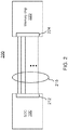
- Figure 2 is an illustration of an example application of the SoC 100 of Figure 1 , according to one embodiment.
- Figure 2 illustrates a system 200 in which SoC 100 is in communication with a memory chip 220. SoC 100 communicates with memory chip 220 over transmission channels 215.
- Memory chip 220 in this example includes any appropriate memory chip for use in a computing device with SoC 100. Examples include a DDR SDRAM chip. A Static Random Access Memory (SRAM) chip, a Dynamic Random Access Memory (DRAM) chip, and an electrically erasable programmable read-only memory (Flash memory) chip, although the scope of embodiments is not limited to any particular memory chip.
- SRAM Static Random Access Memory
- DRAM Dynamic Random Access Memory
- Flash memory electrically erasable programmable read-only memory
- memory chip 220 receives data from SoC 100 over transmission channels (data lines) 215, and a memory controller at memory chip 220 then stores that data in memory cells of the memory chip.
- memory chip 220 receives a read request for specific data from SoC 100, and the memory controller of memory chip 220 then accesses the data from various memory cells of the memory chip and transmits those bits of data to the SoC 100 over transmission channels 215.
- the system of Figure 2 may include implementations of the systems shown in Figures 1 and 3 .
- system 200 of Figure 2 is operated according to one or more DDR standards, where memory chip 220 is a DDR SDRAM chip.
- Memory chip 220 includes a multitude of interface circuits configured to transmit and receive data over respective transmission channels 215. It is expected that there would be many interface circuits at memory chip 220, so the interface circuits are shown collectively as TX/RX circuits 224.
- Each one of the interface circuits operates as described below with respect to Figure 3 , including having an adjustable power source and a selectable termination impedance.
- Each one of the individual transmission channels 215 are the same as or similar to transmission channel 320 of Figure 3 , including having a characteristic impedance.
- SoC 100 also has a multitude of interface circuits configured to transmit and receive data over respective transmission channels 215. Interface circuits of SOC 100 are shown collectively in this example as TX/RX 212. Each one of the interface circuits operates as described below with respect to Figure 3 , including having an adjustable power source and a selectable termination impedance. Memory circuitry 140 of Figure 1 includes TX/RX circuits 212.
- Figure 3 is an illustration of an interface circuit of an SoC coupled to an interface circuit of a memory chip, according to one embodiment.
- the left side of Figure 3 is an illustration of interface circuit 380 implemented on SOC 100, and in this example represents one of the interface circuits at TX/RX circuits 212 Figure 2 .
- the right side of Figure 3 is an illustration of an interface circuit 390 implemented on memory chip 220, and in this example represents one of the interface circuits at TX/RX circuits 224.
- the interface circuits 380, 390 are coupled by a transmission channel 320, which corresponds to one of the transmission channels 215 of Figure 2 .
- Transmission channel 320 provides a data link between SoC 100 and memory chip 220.
- Transmission channel 320 may be embodied in any appropriate structure, for example, a cable, a metal trace on a printed circuit board, a metal wire connecting chips in a package, vias and metal traces connecting an SoC package to a memory chip package, and the like.
- transmission channel 320 is shown as a transmission line in order to emphasize its similarities with transmission lines in general, including having a characteristic impedance as well as a Resistance-Capacitance (RC) time constant.
- the impedance introduced by termination mode operates to match an impedance of an interface circuit to the characteristic impedance of transmission channel 320.
- pull-up device 310a is shown as an NFET, as are pull-down device 312a and on-die termination device 314a.
- Power supply 304a provides a voltage source for VDDQ.
- Power supply 304a is configured to be adjustable so that it can provide at least two voltage levels, as described further below.
- Control circuit 302a provides a control signal to the power supply 304a to direct power supply 304a to apply a first voltage level during a terminated mode and a second voltage level in an unterminated mode.
- Interface circuit 390 is configured similarly to interface circuit 380. Specifically, pull-up device 310 b, pull-down device 312b, and on-die termination device 314b are shown in this example as NFET devices.
- Power supply 304b is an adjustable voltage source that receives a control signal from control circuit 302b. Control circuit 302b provides the control signal to a power supply 304b to direct power supply 304b to apply the first voltage level during the terminated mode and a second voltage level in the unterminated mode.
- control circuits 302a and 302b may be in electrical communication so that they can coordinate terminated and unterminated modes. For instance, in an example where control circuit 302a determines that it should change from a terminated mode to an unterminated mode (or vice versa), control circuit 302a may send a control signal to control circuit 302b informing control circuit 302b of the appropriate terminated or unterminated mode.
- each of interface circuit 380 and interface circuit 390 are configured to be operated in both a transmit and a receive mode. Therefore, control circuit 302b is also configured to determine whether a terminated or unterminated mode is appropriate and to send control signals to control circuit 302a to coordinate operation.
- interface circuit 380 is illustrative of one of a multitude of interface circuits at SoC 100
- interface circuit 390 is illustrative of one of a multitude of interface circuits at memory chip 220.
- control circuit 302a and power supply 304a may serve more than one interface circuit at SoC 100
- control circuit 302b and power supply 304b may serve more than one interface circuit at memory chip 220.
- the various interface circuits at SoC 100 may share the same VDDQ and VSSQ power and ground rails
- the various interface circuits at memory chip 220 may share the same VDDQ and VSSQ power and ground rails.
- FIG. 3 shows devices 310, 312, and 314 as NFET devices, although the scope of embodiments is not so limited. Rather, other embodiments may use a combination of p-type devices and n-type devices (such as a complementary metal oxide semiconductor or CMOS embodiment), just p-type devices, or any other appropriate device operable to act as a switch.
- Power supplies 304 may include any appropriate power supply, such as a switched mode power supply (SMPS), a linear dropout (LDO) voltage regulator, or the like.
- SMPS switched mode power supply
- LDO linear dropout
- Control circuits 302 provide control signals to power supplies 304.
- the logic that is used to determine whether to operate in a terminated mode or an unterminated mode and to provide appropriate control signals in furtherance of the selected mode may be implemented in hardware, software, or a combination of hardware and software. Such logic may be provided as machine-executable code stored in a tangible medium, such as RAM on the SoC 100 or memory chip 220.
- interface circuit 380 is acting as a transmitter to transmit data bits via transmission channel 320 to interface circuit 390 at memory chip 220.
- Control circuits 302 would therefore communicate to coordinate that interface circuit 380 is operating in a transmit mode and to coordinate either a terminated mode or an unterminated mode of operation.
- interface circuits 380, 390 start in a terminated mode. Accordingly, on-die termination device 314b is turned on (device 314a is off).
- Power supply 304a operates at a first voltage level, which is a higher voltage level relative to the second voltage level that is used during an unterminated mode.
- the first voltage level for VDDQ may be 1.1 V or other appropriate level.
- the signal being transferred is a binary one (high signal)
- pull-up device 310a is on (pull-down device 312a is off)
- devices 310a and 314b act as a voltage divider, and the voltage seen at the receive side is around 350 mV, taking into account the threshold voltage of device 310a as a voltage drop on the source voltage.
- pull-down device 312a is on (device 310a is off)
- the voltage seen at the receive side is around 0 V.
- the voltage swing seen at the receive node is approximately 350 mV.
- terminated mode is appropriate for high-speed data transfer (e.g., in the range of GHz), whereas unterminated mode is more appropriate for low speed data transfer (e.g., in the range of 100s of MHz). Therefore, when SOC 100 determines that it is going to switch to a low speed data transfer, it informs control circuits 302a and 302b, which send control signals to the respective power supplies 304a and 304b to lower the voltage level of VDDQ. The interface circuits 380, 390 switch to an unterminated mode, where both termination devices 314a and 314b are off.
- pull-up device 310a When the signal being transferred is a binary one (high signal), pull-up device 310a is on, but the voltage is not divided by terminating resistance and is sensed at the receive side as VDDQ minus the threshold voltage of pull-up device 310a. In the present embodiment, it may be desired that the voltage swing in the unterminated mode be approximately 350 mV, and if the threshold voltage for pull-up device 310a is approximately 150 mV, the voltage applied by power supplies 304a and 304b may be lowered to approximately 500 mV in the unterminated mode.
- control circuit 302a sends a control signal to power supply 304a to cause power supply 304a to apply the first voltage level (e.g., 1.1 V) at the power rail.
- control circuit 302a sends the control signal to the power supply 304a to cause power supply 304a to change its voltage level so that it applies the second voltage level (e.g., 500 mV or lower) at the power rail.
- the SOC 100 may from time to time switch between a terminated mode of operation and an unterminated mode of operation, thereby providing at least two different voltage levels at the power rails as appropriate to the particular termination mode.
- interface circuit 390 may act as a transmitter, and interface circuit 380 may act as a receiver. Therefore, the actions described above with respect to interface circuit 390 apply just as well to interface circuit 380 when 380 act as a receiver. For instance, in a terminated mode of operation, power supply 304b applies the first voltage to the power rail as VDDQ, and termination device 314a is on (termination device 314b is off). In an unterminated mode of operation, power supply 304b applies the second voltage to the power rail as VDDQ, and both termination devices 314a and 314b are off.
- Logic determines when to switch between high-speed terminated mode and low-speed unterminated mode. Also, while Figure 3 is directed toward describing a use case at a single set of interfaces sharing a common transmission line, it is understood that the same or similar actions occur at the interfaces that are associated with the other transmission lines for each bit of data that is communicated between SoC 100 and memory chip 220.
- Various embodiments may provide one or more advantages over conventional systems. For instance, some conventional systems do switch between a terminated high-speed mode and an unterminated low-speed mode, but such conventional systems use the same voltage level as VDDQ for both modes.
- the terminated mode experiences DC power loss because of the use of the termination device.
- the unterminated mode does not have DC power loss from the termination device (because the termination device is off), but an increased voltage swing incurs AC power losses that are greater than the AC power losses in the terminated mode. In fact, AC power losses increase with the square of the voltage level, so that AC power losses may become significant as voltage swing increases.
- the embodiments described above with respect to Figures 1-3 change the value of the VDDQ voltage depending on the speed and the on-die termination setting.
- the output voltage will be limited to the value of VDDQ, thus saving power by keeping the AC component of the power to the same as in terminated mode.
- the NFET drivers of Figure 3 may work well for a wide range of VDDQ voltage levels.
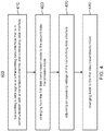
- FIG. 4 A flow diagram of an example method 400 of transmitting and receiving data using the system of Figure 3 is illustrated in Fig. 4 , according to one embodiment.
- the method 400 begins in block 410 in which a transmitting data interface transmits a data signal to a receiving data interface over a transmission channel.
- Data interface 380 transmits data bits across transmission line 320.
- Data interface 380 includes device 314b to provide a selectable on-die termination resistance. Device 314b can be turned on for a terminated transmission mode and turned off for an unterminated transmission mode. Assuming that the system is in a terminated mode, then the on-die termination device 314b is on.
- Transmitting the data signal at block 410 includes applying a high-voltage or a low voltage (a binary one or a binary zero) to the transmission channel 320 to be received by the data interface 390. For instance, turning on the pull-up device 310a applies a binary one, whereas turning on pull-down device 312a (while turning off pull-up device 310a) applies a binary zero.
- memory chip 220 includes a component to capture the data, such as a latching receiver.
- action 410 may also include capturing the data signal at the receive side.
- the system changes from the first data transmission mode to the second data transmission mode.
- the system is in a terminated mode and changes to the unterminated mode, including turning off the on-die termination resistance (device 314b) so that it does not load the line and changing a speed at which the data signal is transmitted.
- the terminated mode includes higher data transmission rates than does the unterminated mode.
- the scope of embodiments may include any appropriate data transmission speed for a given mode.
- the determination as to whether to change from the first data transmission mode to the second data transmission mode may be made according to programmed functionality in the SOC 100 or the memory chip 220.
- some conventional systems employing LPDDR4 include a high-speed terminated mode and a low-speed unterminated mode, where such conventional systems include programmed algorithms to determine which mode to use.
- the scope of embodiments includes using any appropriate algorithms, now known or later developed, to determine to change transmission modes at block 420.
- the system adjusts an operating voltage of the transmitting data interface.
- the power supply 304a receives a control signal from the control circuit 302a instructing it to lower the voltage it applies to the power rail.
- the operating voltage includes the voltage level at VDDQ, where the pull-up and pull-down devices 310a and 312a are disposed between VDDQ and VSSQ (complementary voltage or ground).
- interface circuits 380, 390 are operating in the low-speed, unterminated mode and at the lower, second voltage level.
- block 440 the system changes back to the first data transmission mode.
- the interface circuits 380, 390 may operate at the low-speed, unterminated mode for some amount of time until logic at either the SOC 100 or the data chip 220 determines that the high-speed, terminated operating mode is more appropriate.
- block 440 includes turning on on-die termination resistance (device 314b), and power supply 304a returns the voltage to the first voltage level in response to a control signal from control circuit 302a.
- embodiments are not limited to the specific method shown in Fig. 11.
- Other embodiments may add, omit, rearrange, or modify one or more actions.
- the actions of blocks 410-440 are not performed in a strict series.
- the data signal transmission of action 410 is performed at both data transmission modes.
- method 400 is performed continually while a processor chip and a memory chip transmit data back and forth, and increases or decreases in activity may correspond to various processing tasks.
- on-die termination resistance device 314a
- power supply 304b would change the operating voltage of interface circuit 390 in accordance with the particular terminated or unterminated transmission mode.
- method 400 would be performed at each of those transmission channels.
Landscapes
- Engineering & Computer Science (AREA)
- Theoretical Computer Science (AREA)
- General Engineering & Computer Science (AREA)
- General Physics & Mathematics (AREA)
- Physics & Mathematics (AREA)
- Computer Hardware Design (AREA)
- Power Engineering (AREA)
- Computer Networks & Wireless Communication (AREA)
- Signal Processing (AREA)
- Computing Systems (AREA)
- Microelectronics & Electronic Packaging (AREA)
- Dram (AREA)
- Power Sources (AREA)
- Memory System (AREA)
- Logic Circuits (AREA)
- Dc Digital Transmission (AREA)
Abstract
Description
- The present application claims priority to
U.S. Nonprovisional Application No. 14/863,890, filed September 24, 2015 - This application relates to memory interfaces with processor devices, and more particularly, to memory interfaces having an adjustable voltage and termination.
- Synchronous dynamic random-access memory (SDRAM) is one class of memory used in mobile communication and computing devices, such as smart phones and tablet computers. In some embodiments, double data rate SDRAM (DDR SDRAM or DDR) refers to a type of memory and an associated interface for communicating with the memory. Furthermore, low power DDR (LPDDR or simply LP), sometimes referred to as mobile DDR, is a class of DDR designed to reduce power consumption, with mobile devices being a target application. There are several versions of LPDDR corresponding to various data speeds and power requirements. For example, LPDDR3 (also sometimes denoted as LP3) and LPDDR4 (also sometimes denoted as LP4) are two recent versions of LPDDR. LPDDR4 is designed to communicate at a higher speed and consume less power than LPDDR3 at the expense of increased cost and/or complexity.
- A trend in modern mobile devices, such as smartphones, is to focus memory designs on ever greater memory transfer rate while at the same time conserving power. A system on chip (SoC) is often used in mobile devices to conserve power and/or minimize space requirements. A SoC refers to multiple functional blocks, such as modems and application processor cores, embedded on a single substrate, allowing mobile devices to execute complex and power intensive applications. The single substrate is sometimes referred to as a die, so multiple functional blocks are commonly implemented on a single die.
- The current generation of low power double data rate (LPDDR4) DRAM uses n-type Field Effect Transistors (NFETs) for both the pull-up and pull-down driver in its interface. In addition, an on-die termination (ODT) device (such as a transistor) may be switched on when receiving data to present a desired impedance to a receive line. This is commonly referred to as the terminated mode. The pull-up and pull-down transistors are tuned to also present the desired impedance (e.g., 50 Ohms) when they are switched on during data transmission.
- The power supply voltage (VDDQ) for a conventional LPDDR4 interface is typically around 1.1V. In a terminated high-speed mode of operation in which the ODT transistor is active in the receiving node, the pull-up transistor in the transmitting device and the ODT transistor in the receiving device effectively form a voltage divider that divides the source voltage for the pull-up transistor by one-half. The source voltage for the pull-up transistor when active is VDDQ minus its threshold voltage such that the source voltage varies between a minimum of 550 mV to a maximum of 888 mV (the average being around 720 mV). Due to the voltage divider formed as just discussed, the receiving device will thus receive a voltage of approximately 350 mV on average when the pull-up device is active. When the pull-down device is active, the received voltage is ground such that the voltage swing at the receiving node for the terminated high-speed mode is approximately 350 mV.
- But the active ODT device in the terminated mode consumes DC power. Thus, if the current data transmission does not require the bandwidth of the terminated high-speed mode, an unterminated reduced speed mode may be used. In the unterminated mode, the ODT device is switched off. Since the receiving device has its ODT device turned off in the unterminated mode, there is very little or no consumption of DC power. But the voltage swing is then equal to the source voltage of the pull-up device (550 mv to 888 mv as just described). The AC power is proportional to the square of the voltage swing such that the AC power consumption in the unterminated mode is approximately four times what the AC power consumption is in the terminated mode.
- There is thus a need in the art for improved unterminated modes for memory interfaces.
- Memory interfaces with adjustable operating voltages are disclosed. In one example, a transmit and receive memory interface has an adjustable power supply and a selectable on-die termination resistance. The memory interface is coupled to a data transmission line and another transmit and receive memory interface that also has an adjustable power supply and a selectable on-die termination. Either one of the memory interfaces may be used for transmitting or receiving and may be used in a terminated or unterminated mode. The memory interface that is transmitting may adjust its voltage according to whether it is in a terminated or unterminated data transmission mode.
- In one embodiment, a memory interface includes a pull-up device and a pull-down device, wherein the pull-up device couples between a power rail and a data line, and wherein the pull-down device couples between the data line and ground. The memory interface also includes a power supply configured to supply a first power supply voltage to the power rail during a terminated data transmission mode in which a receiving memory interface coupled to the data line has an active on-die termination. The power supply is further configured to supply a second power supply voltage to the power rail during an unterminated data transmission mode in which the on-die termination does not load the data line, the second power supply voltage being less than the first power supply voltage.
- In another embodiment, a method includes transmitting a data signal at a transmitting data interface that is in communication with a transmission channel and a receiving data interface. The receiving data interface has an on-die termination resistance that is configured to be turned on for a first data transmission mode and turned off for a second data transmission mode. The method further includes changing from the first data transmission mode to the second data transmission mode, including changing a speed at which the data signal is transmitted, and in response to changing from the first data transmission mode to the second data transmission mode, adjusting an operating voltage of the transmitting data interface.
- In yet another embodiment, a memory interface includes means for transmitting a binary one and means for transmitting a binary zero, wherein the means for transmitting the binary one couples between a power rail and a data line, and wherein the means for transmitting a binary zero couples between the data line and ground. The memory interface also includes means for applying a first power supply voltage to the power rail during a terminated data transmission mode in which a receiving memory interface coupled to the data line has an active on-die termination, and for applying a second power supply voltage to the power rail during an unterminated data transmission mode in which the on-die termination does not load the data line. The second power supply voltage is less than the first power supply voltage.
- In yet another embodiment, a memory interface circuit includes a first transmit and receive data interface that is in communication with a second transmit and receive data interface over a transmission channel, wherein the second transmit and receive data interface includes a selectable on-die termination resistance configured to be turned on in a first data transmission mode and turned off in a second data transmission mode. The memory interface circuit also includes a power supply in communication with the first transmit and receive data interface and configured to apply a first voltage level for the first data transmission mode and to apply a second voltage level for the second data transmission mode, where the second voltage level is lower than the first voltage level.
-
-
Fig. 1 is an architectural diagram illustrating an example SoC die and corresponding architecture in accordance with an embodiment of the disclosure. -
Fig. 2 illustrates an example processing chip in communication with a memory chip using multiple interfaces in accordance with an embodiment of the disclosure. -
Fig. 3 illustrates an example system including an interface circuit at a processing chip in an interface circuit at a memory chip connected by a transmission channel for data in accordance with an embodiment of the disclosure. -
Fig. 4 illustrates an example method for changing a voltage based on a terminated or unterminated transmission mode in accordance with an embodiment of the disclosure. - Disclosed herein are embodiments of a memory interface that includes an adjustable power supply and an on-die termination component. To reduce the AC power consumption in a memory interface, the VDDQ supply voltage as discussed above is no longer maintained constant across the terminated and unterminated modes. Instead, the power supply controlling the VDDQ rail is configured to lower the VDDQ supply voltage when the unterminated mode is active and to use a higher level (e.g., the conventional 1.1V) when the terminated mode is active. For example, the power supply may include either a linear dropout regulator (LDO) or a switching power supply that is configured to respond to an indication that the unterminated mode is active by dropping the VDDQ level. As discussed above, the terminated mode (a.k.a. the terminated data transmission mode) commonly refers to a data transmission mode in which an ODT device (e.g., a transistor) is turned on at the receiving side, whereas the unterminated mode (a.k.a. the unterminated data transmission mode) commonly refers to a data transmission mode in which the ODT device is turned off at the receiving side.
- In one aspect of the disclosure, VDDQ during the unterminated mode may be one-half the level used for VDDQ during the terminated mode. For example, if VDDQ equals approximately 1.1V during the terminated mode, it may be dropped to a level such that the voltage swing is still approximately 350 mV during the unterminated mode. In another implementation, VDDQ may be dropped from 1.1V to approximately 888 mV when switching from the terminated mode to the unterminated mode. The scope of embodiments is not limited to any particular voltage level for VDDQ at the power rail or VSSQ, as other voltage levels or values may be adopted as appropriate in alternate implementations; the scope of embodiments is also not limited to any particular value for voltage swing. In fact, the voltage values provided herein are for illustration only, and it is understood that various embodiments may use any appropriate voltage, whether lower or higher than those example values mentioned in this disclosure.
-
Fig. 1 is an architectural diagram illustrating an example system-on-chip (SOC) 100 die and corresponding architecture. In an embodiment, the SoC die 100 is used in a smartphone, a tablet computer, or other mobile wireless device. The SoC die 100 includes a number of functional blocks, including a multi-core processor 110 (sometimes referred to as a central processing unit or CPU), agraphics processor 120, amodem 130, and amemory circuitry 140 as shown inFig. 1. Fig. 1 is a logical layout of an SoC die 100 that shows each of the areas 110-140 for the noted functions as separate and distinct areas, but the actual physical layout may be more complex with, for example, circuitry of one functional block interspersed among circuitry for another functional block. - In an embodiment, the
modem 130 implements baseband processing for any of a number of known wireless technologies or standards, such as long term evolution (LTE). The processors 110-130 refer to areas of the SoC die 100 devoted to those functional blocks. In each of these areas, there is circuitry for the designated function. Thememory circuitry 140 may refer to an area of the SoC die 100 devoted to memory controller and interface circuits for interfacing to an external memory. The external memory may, for example, be housed in a package with interfaces for connecting to thememory circuitry 140. Thememory circuitry 140 can be configured to interface with any type of memory, such as a DDR SDRAM, DRAM, or flash memory. For the purposes of illustration this disclosure focuses on DDR SDRAM, such as LPDDR3 and LPDDR4, but the scope of embodiments is not limited to any particular memory technology or standard. At least one of multi-core processor 110,graphics processor 120, andmodem 130 is in communication withmemory circuitry 140. The various components 110-140 may communicate via any form of known connection, such as a bus. -
Memory circuitry 140 includes a multitude of interfaces that transmit and receive data to and from one or more memory chips. Such a relationship is shown in more detail with respect toFigure 2 , which shows multiple data transmission lines between an SOC and a memory chip. As noted above, each memory interface may include a termination component that may be turned on and off as well as an adjustable power supply that is configured to change a voltage level as the interface changes from terminated to unterminated and vice versa. The scope of embodiments is not limited to any particular SoC architecture, nor even to a multi-core system, andSoC 100 is shown as an example. In fact, various embodiments may be adapted for any type of interface between a processing circuit and a memory circuit. -
Figure 2 is an illustration of an example application of theSoC 100 ofFigure 1 , according to one embodiment.Figure 2 illustrates asystem 200 in whichSoC 100 is in communication with amemory chip 220.SoC 100 communicates withmemory chip 220 overtransmission channels 215. -
Memory chip 220 in this example includes any appropriate memory chip for use in a computing device withSoC 100. Examples include a DDR SDRAM chip. A Static Random Access Memory (SRAM) chip, a Dynamic Random Access Memory (DRAM) chip, and an electrically erasable programmable read-only memory (Flash memory) chip, although the scope of embodiments is not limited to any particular memory chip. During a write operation,memory chip 220 receives data fromSoC 100 over transmission channels (data lines) 215, and a memory controller atmemory chip 220 then stores that data in memory cells of the memory chip. During a read operation,memory chip 220 receives a read request for specific data fromSoC 100, and the memory controller ofmemory chip 220 then accesses the data from various memory cells of the memory chip and transmits those bits of data to theSoC 100 overtransmission channels 215. - The system of
Figure 2 may include implementations of the systems shown inFigures 1 and3 . In one example,system 200 ofFigure 2 is operated according to one or more DDR standards, wherememory chip 220 is a DDR SDRAM chip.Memory chip 220 includes a multitude of interface circuits configured to transmit and receive data overrespective transmission channels 215. It is expected that there would be many interface circuits atmemory chip 220, so the interface circuits are shown collectively as TX/RX circuits 224. Each one of the interface circuits operates as described below with respect toFigure 3 , including having an adjustable power source and a selectable termination impedance. Each one of theindividual transmission channels 215 are the same as or similar totransmission channel 320 ofFigure 3 , including having a characteristic impedance. - Similarly,
SoC 100 also has a multitude of interface circuits configured to transmit and receive data overrespective transmission channels 215. Interface circuits ofSOC 100 are shown collectively in this example as TX/RX 212. Each one of the interface circuits operates as described below with respect toFigure 3 , including having an adjustable power source and a selectable termination impedance.Memory circuitry 140 ofFigure 1 includes TX/RX circuits 212. -
Figure 3 is an illustration of an interface circuit of an SoC coupled to an interface circuit of a memory chip, according to one embodiment. - The left side of
Figure 3 is an illustration ofinterface circuit 380 implemented onSOC 100, and in this example represents one of the interface circuits at TX/RX circuits 212Figure 2 . The right side ofFigure 3 is an illustration of aninterface circuit 390 implemented onmemory chip 220, and in this example represents one of the interface circuits at TX/RX circuits 224. Theinterface circuits transmission channel 320, which corresponds to one of thetransmission channels 215 ofFigure 2 . -
Transmission channel 320 provides a data link betweenSoC 100 andmemory chip 220.Transmission channel 320 may be embodied in any appropriate structure, for example, a cable, a metal trace on a printed circuit board, a metal wire connecting chips in a package, vias and metal traces connecting an SoC package to a memory chip package, and the like. InFigure 3 ,transmission channel 320 is shown as a transmission line in order to emphasize its similarities with transmission lines in general, including having a characteristic impedance as well as a Resistance-Capacitance (RC) time constant. In this example embodiment, the impedance introduced by termination mode operates to match an impedance of an interface circuit to the characteristic impedance oftransmission channel 320. - Referring to
interface circuit 380, pull-updevice 310a is shown as an NFET, as are pull-down device 312a and on-die termination device314a. Power supply 304a provides a voltage source forVDDQ. Power supply 304a is configured to be adjustable so that it can provide at least two voltage levels, as described further below.Control circuit 302a provides a control signal to thepower supply 304a to directpower supply 304a to apply a first voltage level during a terminated mode and a second voltage level in an unterminated mode. -
Interface circuit 390 is configured similarly tointerface circuit 380. Specifically, pull-updevice 310 b, pull-down device 312b, and on-die termination device 314b are shown in this example as NFET devices.Power supply 304b is an adjustable voltage source that receives a control signal fromcontrol circuit 302b.Control circuit 302b provides the control signal to apower supply 304b to directpower supply 304b to apply the first voltage level during the terminated mode and a second voltage level in the unterminated mode. - Although not shown in
Figure 3 ,control circuits control circuit 302a determines that it should change from a terminated mode to an unterminated mode (or vice versa),control circuit 302a may send a control signal to controlcircuit 302b informingcontrol circuit 302b of the appropriate terminated or unterminated mode. - Furthermore, each of
interface circuit 380 andinterface circuit 390 are configured to be operated in both a transmit and a receive mode. Therefore,control circuit 302b is also configured to determine whether a terminated or unterminated mode is appropriate and to send control signals to controlcircuit 302a to coordinate operation. - As noted above,
interface circuit 380 is illustrative of one of a multitude of interface circuits atSoC 100, andinterface circuit 390 is illustrative of one of a multitude of interface circuits atmemory chip 220. In some embodiments,control circuit 302a andpower supply 304a may serve more than one interface circuit atSoC 100, andcontrol circuit 302b andpower supply 304b may serve more than one interface circuit atmemory chip 220. Or put another way, in some embodiments, the various interface circuits atSoC 100 may share the same VDDQ and VSSQ power and ground rails, and the various interface circuits atmemory chip 220 may share the same VDDQ and VSSQ power and ground rails. -
Figure 3 shows devices 310, 312, and 314 as NFET devices, although the scope of embodiments is not so limited. Rather, other embodiments may use a combination of p-type devices and n-type devices (such as a complementary metal oxide semiconductor or CMOS embodiment), just p-type devices, or any other appropriate device operable to act as a switch. Power supplies 304 may include any appropriate power supply, such as a switched mode power supply (SMPS), a linear dropout (LDO) voltage regulator, or the like. - Control circuits 302, as noted above, provide control signals to power supplies 304. The logic that is used to determine whether to operate in a terminated mode or an unterminated mode and to provide appropriate control signals in furtherance of the selected mode may be implemented in hardware, software, or a combination of hardware and software. Such logic may be provided as machine-executable code stored in a tangible medium, such as RAM on the
SoC 100 ormemory chip 220. - In one example use case,
interface circuit 380 is acting as a transmitter to transmit data bits viatransmission channel 320 tointerface circuit 390 atmemory chip 220. Control circuits 302 would therefore communicate to coordinate thatinterface circuit 380 is operating in a transmit mode and to coordinate either a terminated mode or an unterminated mode of operation. For purposes of this example, it is assumed thatinterface circuits -
Power supply 304a operates at a first voltage level, which is a higher voltage level relative to the second voltage level that is used during an unterminated mode. For example, the first voltage level for VDDQ may be 1.1 V or other appropriate level. When the signal being transferred is a binary one (high signal), pull-updevice 310a is on (pull-down device 312a is off), anddevices 310a and 314b act as a voltage divider, and the voltage seen at the receive side is around 350 mV, taking into account the threshold voltage ofdevice 310a as a voltage drop on the source voltage. When the signal being transferred is a binary zero (low signal), pull-down device 312a is on (device 310a is off), and the voltage seen at the receive side is around 0 V. Thus, in terminated mode, the voltage swing seen at the receive node is approximately 350 mV. - In some LPDDR4 embodiments, terminated mode is appropriate for high-speed data transfer (e.g., in the range of GHz), whereas unterminated mode is more appropriate for low speed data transfer (e.g., in the range of 100s of MHz). Therefore, when
SOC 100 determines that it is going to switch to a low speed data transfer, it informscontrol circuits respective power supplies interface circuits device 310a is on, but the voltage is not divided by terminating resistance and is sensed at the receive side as VDDQ minus the threshold voltage of pull-updevice 310a. In the present embodiment, it may be desired that the voltage swing in the unterminated mode be approximately 350 mV, and if the threshold voltage for pull-updevice 310a is approximately 150 mV, the voltage applied bypower supplies - Continuing with the example, during the terminated mode of operation,
control circuit 302a sends a control signal topower supply 304a to causepower supply 304a to apply the first voltage level (e.g., 1.1 V) at the power rail. During the unterminated mode of operation,control circuit 302a sends the control signal to thepower supply 304a to causepower supply 304a to change its voltage level so that it applies the second voltage level (e.g., 500 mV or lower) at the power rail. AsSoC 100 issues read and write operations tomemory chip 220, the SOC 100 (and possibly memory chip 220) may from time to time switch between a terminated mode of operation and an unterminated mode of operation, thereby providing at least two different voltage levels at the power rails as appropriate to the particular termination mode. - Further in this example,
interface circuit 390 may act as a transmitter, andinterface circuit 380 may act as a receiver. Therefore, the actions described above with respect tointerface circuit 390 apply just as well tointerface circuit 380 when 380 act as a receiver. For instance, in a terminated mode of operation,power supply 304b applies the first voltage to the power rail as VDDQ, and termination device 314a is on (termination device 314b is off). In an unterminated mode of operation,power supply 304b applies the second voltage to the power rail as VDDQ, and both termination devices 314a and 314b are off. - Logic, either at
control circuits SoC 100 ormemory chip 220, determines when to switch between high-speed terminated mode and low-speed unterminated mode. Also, whileFigure 3 is directed toward describing a use case at a single set of interfaces sharing a common transmission line, it is understood that the same or similar actions occur at the interfaces that are associated with the other transmission lines for each bit of data that is communicated betweenSoC 100 andmemory chip 220. - Various embodiments may provide one or more advantages over conventional systems. For instance, some conventional systems do switch between a terminated high-speed mode and an unterminated low-speed mode, but such conventional systems use the same voltage level as VDDQ for both modes. The terminated mode experiences DC power loss because of the use of the termination device. The unterminated mode does not have DC power loss from the termination device (because the termination device is off), but an increased voltage swing incurs AC power losses that are greater than the AC power losses in the terminated mode. In fact, AC power losses increase with the square of the voltage level, so that AC power losses may become significant as voltage swing increases.
- By contrast, the embodiments described above with respect to
Figures 1-3 change the value of the VDDQ voltage depending on the speed and the on-die termination setting. By lowering the VDDQ voltage when in the unterminated mode the output voltage will be limited to the value of VDDQ, thus saving power by keeping the AC component of the power to the same as in terminated mode. Furthermore, the NFET drivers ofFigure 3 may work well for a wide range of VDDQ voltage levels. - A flow diagram of an
example method 400 of transmitting and receiving data using the system ofFigure 3 is illustrated inFig. 4 , according to one embodiment. Themethod 400 begins inblock 410 in which a transmitting data interface transmits a data signal to a receiving data interface over a transmission channel. - An example is shown in
Figure 3 , in which data interface 380 is in transmitting mode and data interface 390 is in receiving mode.Data interface 380 transmits data bits acrosstransmission line 320.Data interface 380 includes device 314b to provide a selectable on-die termination resistance. Device 314b can be turned on for a terminated transmission mode and turned off for an unterminated transmission mode. Assuming that the system is in a terminated mode, then the on-die termination device 314b is on. - Transmitting the data signal at
block 410 includes applying a high-voltage or a low voltage (a binary one or a binary zero) to thetransmission channel 320 to be received by thedata interface 390. For instance, turning on the pull-updevice 310a applies a binary one, whereas turning on pull-down device 312a (while turning off pull-updevice 310a) applies a binary zero. Although not shown inFigure 3 , it is understood thatmemory chip 220 includes a component to capture the data, such as a latching receiver. Thus,action 410 may also include capturing the data signal at the receive side. - Next in
block 420, the system changes from the first data transmission mode to the second data transmission mode. Continuing with the example, the system is in a terminated mode and changes to the unterminated mode, including turning off the on-die termination resistance (device 314b) so that it does not load the line and changing a speed at which the data signal is transmitted. In an example that includes LPDDR4, the terminated mode includes higher data transmission rates than does the unterminated mode. However, the scope of embodiments may include any appropriate data transmission speed for a given mode. - The determination as to whether to change from the first data transmission mode to the second data transmission mode may be made according to programmed functionality in the
SOC 100 or thememory chip 220. For instance, some conventional systems employing LPDDR4 include a high-speed terminated mode and a low-speed unterminated mode, where such conventional systems include programmed algorithms to determine which mode to use. The scope of embodiments includes using any appropriate algorithms, now known or later developed, to determine to change transmission modes atblock 420. - In
block 430, the system adjusts an operating voltage of the transmitting data interface. In the example ofFigure 3 , thepower supply 304a receives a control signal from thecontrol circuit 302a instructing it to lower the voltage it applies to the power rail. In this example, the operating voltage includes the voltage level at VDDQ, where the pull-up and pull-downdevices 310a and 312a are disposed between VDDQ and VSSQ (complementary voltage or ground). At this point,interface circuits - Next in
block 440, the system changes back to the first data transmission mode. For instance, theinterface circuits SOC 100 or thedata chip 220 determines that the high-speed, terminated operating mode is more appropriate. Accordingly, in one example, block 440 includes turning on on-die termination resistance (device 314b), andpower supply 304a returns the voltage to the first voltage level in response to a control signal fromcontrol circuit 302a. - The scope of embodiments is not limited to the specific method shown in Fig. 11. Other embodiments may add, omit, rearrange, or modify one or more actions. For instance, in many real-world applications, the actions of blocks 410-440 are not performed in a strict series. For example, the data signal transmission of
action 410 is performed at both data transmission modes. Furthermore, in many applications,method 400 is performed continually while a processor chip and a memory chip transmit data back and forth, and increases or decreases in activity may correspond to various processing tasks. - It is also understood that the discussion of
method 400, above, applies just as well when thedata chip 220 is in transmission mode (as in a read operation) andSoC 100 is in receiving mode. In such an instance, on-die termination resistance (device 314a) would be turned on during a terminated transmission mode and turned off during an unterminated transmission mode, andpower supply 304b would change the operating voltage ofinterface circuit 390 in accordance with the particular terminated or unterminated transmission mode. Also, it is understood that in a system in which there are multiple data transmission channels (e.g., 32 or 64),method 400 would be performed at each of those transmission channels. - As those of some skill in this art will by now appreciate and depending on the particular application at hand, many modifications, substitutions and variations can be made in and to the materials, apparatus, configurations and methods of use of the devices of the present disclosure without departing from the spirit and scope thereof. In light of this, the scope of the present disclosure should not be limited to that of the particular embodiments illustrated and described herein, as they are merely by way of some examples thereof, but rather, should be fully commensurate with that of the claims appended hereafter and their functional equivalents.
Claims (7)
- A memory interface circuit comprising:a first transmit and receive data interface that is configured to communicate with a second transmit and receive data interface over a transmission channel, wherein the second transmit and receive data interface includes a selectable on-die termination resistance configured to be turned on in a first data transmission mode and turned off in a second data transmission mode;
anda power supply electrically coupled to the first transmit and receive data interface and configured to apply a first voltage level for the first data transmission mode and to apply a second voltage level for the second data transmission mode, where the second voltage level is lower than the first voltage level. - The memory interface circuit of claim 1, further comprising:
another selectable on-die termination resistance included in the first transmit and receive data interface. - The memory interface circuit of claim 1, wherein the first transmit and receive data interface comprises:a pull-up transistor; anda pull-down transistor, wherein the pull-up transistor couples between the power supply and the transmission channel, and wherein the pull-down transistor couples between the transmission channel and ground.
- The memory interface circuit of claim 3, wherein the pull-up transistor and pull-down transistor comprise N-type field effect transistors (NFETs).
- The memory interface circuit of claim 1, wherein the memory interface circuit is included in a system on chip (SoC).
- The memory interface circuit of claim 1, wherein the memory interface circuit is included in a memory chip.
- The memory interface circuit of claim 1, wherein the transmission channel includes a wire in communication between a system on chip and a memory chip.
Applications Claiming Priority (3)
| Application Number | Priority Date | Filing Date | Title |
|---|---|---|---|
| US14/863,890 US9910482B2 (en) | 2015-09-24 | 2015-09-24 | Memory interface with adjustable voltage and termination and methods of use |
| PCT/US2016/051134 WO2017053097A1 (en) | 2015-09-24 | 2016-09-09 | Memory interface with adjustable voltage and termination and methods of use |
| EP16766814.4A EP3353666B1 (en) | 2015-09-24 | 2016-09-09 | Memory interface with adjustable voltage and termination and methods of use |
Related Parent Applications (2)
| Application Number | Title | Priority Date | Filing Date |
|---|---|---|---|
| EP16766814.4A Division EP3353666B1 (en) | 2015-09-24 | 2016-09-09 | Memory interface with adjustable voltage and termination and methods of use |
| EP16766814.4A Division-Into EP3353666B1 (en) | 2015-09-24 | 2016-09-09 | Memory interface with adjustable voltage and termination and methods of use |
Publications (2)
| Publication Number | Publication Date |
|---|---|
| EP3614272A1 true EP3614272A1 (en) | 2020-02-26 |
| EP3614272B1 EP3614272B1 (en) | 2023-03-22 |
Family
ID=56940465
Family Applications (2)
| Application Number | Title | Priority Date | Filing Date |
|---|---|---|---|
| EP16766814.4A Active EP3353666B1 (en) | 2015-09-24 | 2016-09-09 | Memory interface with adjustable voltage and termination and methods of use |
| EP19203349.6A Active EP3614272B1 (en) | 2015-09-24 | 2016-09-09 | Memory interface with adjustable voltage and termination and methods of use |
Family Applications Before (1)
| Application Number | Title | Priority Date | Filing Date |
|---|---|---|---|
| EP16766814.4A Active EP3353666B1 (en) | 2015-09-24 | 2016-09-09 | Memory interface with adjustable voltage and termination and methods of use |
Country Status (7)
| Country | Link |
|---|---|
| US (2) | US9910482B2 (en) |
| EP (2) | EP3353666B1 (en) |
| JP (2) | JP6396627B1 (en) |
| KR (1) | KR101872997B1 (en) |
| CN (2) | CN114397955B (en) |
| BR (1) | BR112018005941A2 (en) |
| WO (1) | WO2017053097A1 (en) |
Families Citing this family (6)
| Publication number | Priority date | Publication date | Assignee | Title |
|---|---|---|---|---|
| US9910482B2 (en) | 2015-09-24 | 2018-03-06 | Qualcomm Incorporated | Memory interface with adjustable voltage and termination and methods of use |
| DE102017103721B4 (en) * | 2017-02-23 | 2022-07-21 | Karl Storz Se & Co. Kg | Device for capturing a stereo image with a rotatable viewing device |
| KR102573219B1 (en) * | 2018-09-14 | 2023-09-01 | 삼성전자주식회사 | An integrated circuit capable of controlling impedance and an electronic device comprising thereof |
| US11409354B2 (en) * | 2019-04-22 | 2022-08-09 | Micron Technology, Inc. | Multi-voltage operation for driving a multi-mode channel |
| US10896143B1 (en) * | 2019-12-19 | 2021-01-19 | Micron Technology, Inc. | Configurable termination circuitry |
| JP2023130669A (en) * | 2022-03-08 | 2023-09-21 | キオクシア株式会社 | semiconductor integrated circuit |
Citations (4)
| Publication number | Priority date | Publication date | Assignee | Title |
|---|---|---|---|---|
| US20070080707A1 (en) * | 2005-09-28 | 2007-04-12 | Brinkman Michael G | Selective on-die termination for improved power management and thermal distribution |
| US20070139071A1 (en) * | 2005-12-19 | 2007-06-21 | Rambus Inc. | Configurable on-die termination |
| US7864183B1 (en) * | 2007-03-08 | 2011-01-04 | Nvidia Corporation | Dynamic switching of memory termination characteristics in a graphics system |
| US20150023112A1 (en) * | 2013-07-19 | 2015-01-22 | Samsung Electronics Co., Ltd. | Integrated circuit and data input method |
Family Cites Families (33)
| Publication number | Priority date | Publication date | Assignee | Title |
|---|---|---|---|---|
| JPH1020974A (en) | 1996-07-03 | 1998-01-23 | Fujitsu Ltd | Bus structure and input / output buffer |
| US6559690B2 (en) | 2001-03-15 | 2003-05-06 | Micron Technology, Inc. | Programmable dual drive strength output buffer with a shared boot circuit |
| JP3808335B2 (en) * | 2001-07-26 | 2006-08-09 | エルピーダメモリ株式会社 | Memory module |
| JP3721117B2 (en) | 2001-10-29 | 2005-11-30 | エルピーダメモリ株式会社 | Input/output circuit, reference voltage generation circuit, and semiconductor integrated circuit |
| US6965529B2 (en) * | 2002-06-21 | 2005-11-15 | Intel Coproration | Memory bus termination |
| KR100464437B1 (en) * | 2002-11-20 | 2004-12-31 | 삼성전자주식회사 | On-Die Termination circuit and method for reducing on-chip DC current and memory system including memory device having the same |
| KR100670702B1 (en) * | 2004-10-30 | 2007-01-17 | 주식회사 하이닉스반도체 | Semiconductor memory device with on-die termination circuit |
| WO2007102135A1 (en) * | 2006-03-09 | 2007-09-13 | Nxp B.V. | Method and system for adjusting interconnect voltage levels in low power high-speed differential interfaces |
| US7945793B2 (en) * | 2006-08-11 | 2011-05-17 | Intel Corporation | Interface frequency modulation to allow non-terminated operation and power reduction |
| TW200910373A (en) * | 2007-06-08 | 2009-03-01 | Mosaid Technologies Inc | Dynamic impedance control for input/output buffers |
| US7764082B2 (en) * | 2007-11-20 | 2010-07-27 | Montage Technology Group Limited | On-die termination circuit |
| KR100933814B1 (en) * | 2008-04-25 | 2009-12-24 | 주식회사 하이닉스반도체 | On die termination test device and on die termination test method |
| JP2010219751A (en) * | 2009-03-16 | 2010-09-30 | Elpida Memory Inc | Semiconductor device |
| KR20100116253A (en) | 2009-04-22 | 2010-11-01 | 삼성전자주식회사 | Input/output circuit and integrated circuit apparatus including the same |
| KR20110003725A (en) * | 2009-07-06 | 2011-01-13 | 삼성전자주식회사 | Transceiver for controlling the swing width of output voltage and its method |
| KR101789077B1 (en) | 2010-02-23 | 2017-11-20 | 삼성전자주식회사 | On-die termination circuit, data output buffer, semiconductor memory device, memory module, method of operating an on-die termination circuit, method of operating a data output buffer and method of training on-die termination |
| US8868826B2 (en) * | 2010-05-20 | 2014-10-21 | Cisco Technology, Inc. | Facilitating communication between memory devices and CPUs |
| US8274308B2 (en) | 2010-06-28 | 2012-09-25 | Intel Corporation | Method and apparatus for dynamic memory termination |
| US9046909B2 (en) | 2011-09-02 | 2015-06-02 | Rambus Inc. | On-chip regulator with variable load compensation |
| JP5733126B2 (en) | 2011-09-15 | 2015-06-10 | 富士通セミコンダクター株式会社 | Memory interface circuit and timing adjustment method |
| US9471518B2 (en) * | 2011-11-03 | 2016-10-18 | Rambus Inc. | Multi-modal memory interface |
| CN103871458B (en) * | 2012-12-07 | 2018-05-01 | 三星电子株式会社 | Integrated circuit and its data processing method, decoder, memory |
| US9525571B2 (en) * | 2013-03-05 | 2016-12-20 | Lattice Semiconductor Corporation | Calibration of single-ended high-speed interfaces |
| US9088445B2 (en) * | 2013-03-07 | 2015-07-21 | Qualcomm Incorporated | Method and apparatus for selectively terminating signals on a bidirectional bus based on bus speed |
| US9599639B2 (en) * | 2013-04-05 | 2017-03-21 | Tektronix, Inc. | Device and method to prevent inter-system interference |
| JP2014241057A (en) | 2013-06-12 | 2014-12-25 | ソニー株式会社 | Interface control circuit, memory system, and method of controlling interface control circuit |
| US9374004B2 (en) | 2013-06-28 | 2016-06-21 | Intel Corporation | I/O driver transmit swing control |
| KR102081565B1 (en) * | 2013-10-07 | 2020-02-26 | 삼성전자 주식회사 | Signaling method using constant reference voltage and devices there-of |
| KR102432754B1 (en) * | 2013-10-21 | 2022-08-16 | 에프엘씨 글로벌 리미티드 | Final level cache system and corresponding method |
| US20160162214A1 (en) * | 2014-12-08 | 2016-06-09 | James A McCall | Adjustable low swing memory interface |
| KR20170028769A (en) * | 2015-09-04 | 2017-03-14 | 에스케이하이닉스 주식회사 | Semiconductor device and semiconductor system |
| US9910482B2 (en) * | 2015-09-24 | 2018-03-06 | Qualcomm Incorporated | Memory interface with adjustable voltage and termination and methods of use |
| US9513655B1 (en) * | 2015-11-24 | 2016-12-06 | Omnivision Technologies, Inc. | Interface circuit with variable output swing and open termination mode for transmitting signals |
-
2015
- 2015-09-24 US US14/863,890 patent/US9910482B2/en active Active
-
2016
- 2016-09-09 BR BR112018005941A patent/BR112018005941A2/en not_active Application Discontinuation
- 2016-09-09 KR KR1020187011466A patent/KR101872997B1/en not_active Expired - Fee Related
- 2016-09-09 CN CN202111509026.5A patent/CN114397955B/en active Active
- 2016-09-09 CN CN201680055256.XA patent/CN108139991B/en active Active
- 2016-09-09 JP JP2018515263A patent/JP6396627B1/en active Active
- 2016-09-09 EP EP16766814.4A patent/EP3353666B1/en active Active
- 2016-09-09 WO PCT/US2016/051134 patent/WO2017053097A1/en not_active Ceased
- 2016-09-09 EP EP19203349.6A patent/EP3614272B1/en active Active
-
2018
- 2018-01-05 US US15/863,155 patent/US10613613B2/en active Active
- 2018-08-29 JP JP2018160670A patent/JP2019012544A/en active Pending
Patent Citations (4)
| Publication number | Priority date | Publication date | Assignee | Title |
|---|---|---|---|---|
| US20070080707A1 (en) * | 2005-09-28 | 2007-04-12 | Brinkman Michael G | Selective on-die termination for improved power management and thermal distribution |
| US20070139071A1 (en) * | 2005-12-19 | 2007-06-21 | Rambus Inc. | Configurable on-die termination |
| US7864183B1 (en) * | 2007-03-08 | 2011-01-04 | Nvidia Corporation | Dynamic switching of memory termination characteristics in a graphics system |
| US20150023112A1 (en) * | 2013-07-19 | 2015-01-22 | Samsung Electronics Co., Ltd. | Integrated circuit and data input method |
Also Published As
| Publication number | Publication date |
|---|---|
| WO2017053097A1 (en) | 2017-03-30 |
| EP3353666B1 (en) | 2020-01-01 |
| CN114397955A (en) | 2022-04-26 |
| KR101872997B1 (en) | 2018-07-02 |
| EP3614272B1 (en) | 2023-03-22 |
| US9910482B2 (en) | 2018-03-06 |
| US10613613B2 (en) | 2020-04-07 |
| EP3353666A1 (en) | 2018-08-01 |
| BR112018005941A2 (en) | 2018-10-16 |
| JP2019012544A (en) | 2019-01-24 |
| CN114397955B (en) | 2025-05-13 |
| KR20180051638A (en) | 2018-05-16 |
| CN108139991A (en) | 2018-06-08 |
| CN108139991B (en) | 2021-12-24 |
| US20170090546A1 (en) | 2017-03-30 |
| US20180129267A1 (en) | 2018-05-10 |
| JP6396627B1 (en) | 2018-09-26 |
| JP2018534663A (en) | 2018-11-22 |
Similar Documents
| Publication | Publication Date | Title |
|---|---|---|
| US10613613B2 (en) | Memory interface with adjustable voltage and termination and methods of use | |
| US9152257B2 (en) | Low swing voltage mode driver | |
| US9024665B2 (en) | Transmitter with voltage and current mode drivers | |
| CN107077302B (en) | Apparatus and method for interfacing with host system | |
| US10162402B2 (en) | Serial communication method | |
| US9647664B2 (en) | Output driver, semiconductor apparatus, system, and computing system using the same | |
| US9088445B2 (en) | Method and apparatus for selectively terminating signals on a bidirectional bus based on bus speed | |
| US9413565B1 (en) | Termination circuit, and interface circuit and system including the same | |
| TWI506757B (en) | Decentralized electrostatic discharge protection for the input/output architecture on the package | |
| US10572431B2 (en) | Data transmission circuit with encoding circuit, and semiconductor apparatus and semiconductor system including the data transmission circuit | |
| US12211580B2 (en) | Termination for pulse amplitude modulation | |
| KR20230160043A (en) | Semiconductor apparatus performing a plurality of clock signaling and semiconductor system including the same | |
| US20130114363A1 (en) | Multi-modal memory interface | |
| US20140253179A1 (en) | Low voltage swing repeater | |
| US12431997B2 (en) | Multiplexer and serializer including the same |
Legal Events
| Date | Code | Title | Description |
|---|---|---|---|
| PUAI | Public reference made under article 153(3) epc to a published international application that has entered the european phase |
Free format text: ORIGINAL CODE: 0009012 |
|
| STAA | Information on the status of an ep patent application or granted ep patent |
Free format text: STATUS: REQUEST FOR EXAMINATION WAS MADE |
|
| 17P | Request for examination filed |
Effective date: 20191015 |
|
| AC | Divisional application: reference to earlier application |
Ref document number: 3353666 Country of ref document: EP Kind code of ref document: P |
|
| AK | Designated contracting states |
Kind code of ref document: A1 Designated state(s): AL AT BE BG CH CY CZ DE DK EE ES FI FR GB GR HR HU IE IS IT LI LT LU LV MC MK MT NL NO PL PT RO RS SE SI SK SM TR |
|
| STAA | Information on the status of an ep patent application or granted ep patent |
Free format text: STATUS: EXAMINATION IS IN PROGRESS |
|
| 17Q | First examination report despatched |
Effective date: 20201126 |
|
| GRAP | Despatch of communication of intention to grant a patent |
Free format text: ORIGINAL CODE: EPIDOSNIGR1 |
|
| STAA | Information on the status of an ep patent application or granted ep patent |
Free format text: STATUS: GRANT OF PATENT IS INTENDED |
|
| INTG | Intention to grant announced |
Effective date: 20210928 |
|
| GRAJ | Information related to disapproval of communication of intention to grant by the applicant or resumption of examination proceedings by the epo deleted |
Free format text: ORIGINAL CODE: EPIDOSDIGR1 |
|
| STAA | Information on the status of an ep patent application or granted ep patent |
Free format text: STATUS: EXAMINATION IS IN PROGRESS |
|
| INTC | Intention to grant announced (deleted) | ||
| GRAP | Despatch of communication of intention to grant a patent |
Free format text: ORIGINAL CODE: EPIDOSNIGR1 |
|
| STAA | Information on the status of an ep patent application or granted ep patent |
Free format text: STATUS: GRANT OF PATENT IS INTENDED |
|
| INTG | Intention to grant announced |
Effective date: 20220930 |
|
| GRAS | Grant fee paid |
Free format text: ORIGINAL CODE: EPIDOSNIGR3 |
|
| GRAA | (expected) grant |
Free format text: ORIGINAL CODE: 0009210 |
|
| STAA | Information on the status of an ep patent application or granted ep patent |
Free format text: STATUS: THE PATENT HAS BEEN GRANTED |
|
| AC | Divisional application: reference to earlier application |
Ref document number: 3353666 Country of ref document: EP Kind code of ref document: P |
|
| AK | Designated contracting states |
Kind code of ref document: B1 Designated state(s): AL AT BE BG CH CY CZ DE DK EE ES FI FR GB GR HR HU IE IS IT LI LT LU LV MC MK MT NL NO PL PT RO RS SE SI SK SM TR |
|
| REG | Reference to a national code |
Ref country code: GB Ref legal event code: FG4D |
|
| RIN1 | Information on inventor provided before grant (corrected) |
Inventor name: SRINIVAS, VAISHNAV Inventor name: ISAKANIAN, PATRICK Inventor name: THILENIUS, STEPHEN Inventor name: BRUNOLLI, MICHAEL |
|
| REG | Reference to a national code |
Ref country code: CH Ref legal event code: EP |
|
| REG | Reference to a national code |
Ref country code: IE Ref legal event code: FG4D |
|
| REG | Reference to a national code |
Ref country code: DE Ref legal event code: R096 Ref document number: 602016078488 Country of ref document: DE |
|
| REG | Reference to a national code |
Ref country code: AT Ref legal event code: REF Ref document number: 1555730 Country of ref document: AT Kind code of ref document: T Effective date: 20230415 |
|
| REG | Reference to a national code |
Ref country code: LT Ref legal event code: MG9D |
|
| REG | Reference to a national code |
Ref country code: NL Ref legal event code: MP Effective date: 20230322 |
|
| PG25 | Lapsed in a contracting state [announced via postgrant information from national office to epo] |
Ref country code: RS Free format text: LAPSE BECAUSE OF FAILURE TO SUBMIT A TRANSLATION OF THE DESCRIPTION OR TO PAY THE FEE WITHIN THE PRESCRIBED TIME-LIMIT Effective date: 20230322 Ref country code: NO Free format text: LAPSE BECAUSE OF FAILURE TO SUBMIT A TRANSLATION OF THE DESCRIPTION OR TO PAY THE FEE WITHIN THE PRESCRIBED TIME-LIMIT Effective date: 20230622 Ref country code: LV Free format text: LAPSE BECAUSE OF FAILURE TO SUBMIT A TRANSLATION OF THE DESCRIPTION OR TO PAY THE FEE WITHIN THE PRESCRIBED TIME-LIMIT Effective date: 20230322 Ref country code: LT Free format text: LAPSE BECAUSE OF FAILURE TO SUBMIT A TRANSLATION OF THE DESCRIPTION OR TO PAY THE FEE WITHIN THE PRESCRIBED TIME-LIMIT Effective date: 20230322 Ref country code: HR Free format text: LAPSE BECAUSE OF FAILURE TO SUBMIT A TRANSLATION OF THE DESCRIPTION OR TO PAY THE FEE WITHIN THE PRESCRIBED TIME-LIMIT Effective date: 20230322 |
|
| REG | Reference to a national code |
Ref country code: AT Ref legal event code: MK05 Ref document number: 1555730 Country of ref document: AT Kind code of ref document: T Effective date: 20230322 |
|
| PG25 | Lapsed in a contracting state [announced via postgrant information from national office to epo] |
Ref country code: SE Free format text: LAPSE BECAUSE OF FAILURE TO SUBMIT A TRANSLATION OF THE DESCRIPTION OR TO PAY THE FEE WITHIN THE PRESCRIBED TIME-LIMIT Effective date: 20230322 Ref country code: NL Free format text: LAPSE BECAUSE OF FAILURE TO SUBMIT A TRANSLATION OF THE DESCRIPTION OR TO PAY THE FEE WITHIN THE PRESCRIBED TIME-LIMIT Effective date: 20230322 Ref country code: GR Free format text: LAPSE BECAUSE OF FAILURE TO SUBMIT A TRANSLATION OF THE DESCRIPTION OR TO PAY THE FEE WITHIN THE PRESCRIBED TIME-LIMIT Effective date: 20230623 Ref country code: FI Free format text: LAPSE BECAUSE OF FAILURE TO SUBMIT A TRANSLATION OF THE DESCRIPTION OR TO PAY THE FEE WITHIN THE PRESCRIBED TIME-LIMIT Effective date: 20230322 |
|
| PG25 | Lapsed in a contracting state [announced via postgrant information from national office to epo] |
Ref country code: SM Free format text: LAPSE BECAUSE OF FAILURE TO SUBMIT A TRANSLATION OF THE DESCRIPTION OR TO PAY THE FEE WITHIN THE PRESCRIBED TIME-LIMIT Effective date: 20230322 Ref country code: RO Free format text: LAPSE BECAUSE OF FAILURE TO SUBMIT A TRANSLATION OF THE DESCRIPTION OR TO PAY THE FEE WITHIN THE PRESCRIBED TIME-LIMIT Effective date: 20230322 Ref country code: PT Free format text: LAPSE BECAUSE OF FAILURE TO SUBMIT A TRANSLATION OF THE DESCRIPTION OR TO PAY THE FEE WITHIN THE PRESCRIBED TIME-LIMIT Effective date: 20230724 Ref country code: ES Free format text: LAPSE BECAUSE OF FAILURE TO SUBMIT A TRANSLATION OF THE DESCRIPTION OR TO PAY THE FEE WITHIN THE PRESCRIBED TIME-LIMIT Effective date: 20230322 Ref country code: EE Free format text: LAPSE BECAUSE OF FAILURE TO SUBMIT A TRANSLATION OF THE DESCRIPTION OR TO PAY THE FEE WITHIN THE PRESCRIBED TIME-LIMIT Effective date: 20230322 Ref country code: AT Free format text: LAPSE BECAUSE OF FAILURE TO SUBMIT A TRANSLATION OF THE DESCRIPTION OR TO PAY THE FEE WITHIN THE PRESCRIBED TIME-LIMIT Effective date: 20230322 |
|
| PG25 | Lapsed in a contracting state [announced via postgrant information from national office to epo] |
Ref country code: SK Free format text: LAPSE BECAUSE OF FAILURE TO SUBMIT A TRANSLATION OF THE DESCRIPTION OR TO PAY THE FEE WITHIN THE PRESCRIBED TIME-LIMIT Effective date: 20230322 Ref country code: PL Free format text: LAPSE BECAUSE OF FAILURE TO SUBMIT A TRANSLATION OF THE DESCRIPTION OR TO PAY THE FEE WITHIN THE PRESCRIBED TIME-LIMIT Effective date: 20230322 Ref country code: IS Free format text: LAPSE BECAUSE OF FAILURE TO SUBMIT A TRANSLATION OF THE DESCRIPTION OR TO PAY THE FEE WITHIN THE PRESCRIBED TIME-LIMIT Effective date: 20230722 |
|
| REG | Reference to a national code |
Ref country code: DE Ref legal event code: R097 Ref document number: 602016078488 Country of ref document: DE |
|
| PLBE | No opposition filed within time limit |
Free format text: ORIGINAL CODE: 0009261 |
|
| STAA | Information on the status of an ep patent application or granted ep patent |
Free format text: STATUS: NO OPPOSITION FILED WITHIN TIME LIMIT |
|
| PG25 | Lapsed in a contracting state [announced via postgrant information from national office to epo] |
Ref country code: SI Free format text: LAPSE BECAUSE OF FAILURE TO SUBMIT A TRANSLATION OF THE DESCRIPTION OR TO PAY THE FEE WITHIN THE PRESCRIBED TIME-LIMIT Effective date: 20230322 Ref country code: DK Free format text: LAPSE BECAUSE OF FAILURE TO SUBMIT A TRANSLATION OF THE DESCRIPTION OR TO PAY THE FEE WITHIN THE PRESCRIBED TIME-LIMIT Effective date: 20230322 Ref country code: CZ Free format text: LAPSE BECAUSE OF FAILURE TO SUBMIT A TRANSLATION OF THE DESCRIPTION OR TO PAY THE FEE WITHIN THE PRESCRIBED TIME-LIMIT Effective date: 20230322 |
|
| 26N | No opposition filed |
Effective date: 20240102 |
|
| REG | Reference to a national code |
Ref country code: CH Ref legal event code: PL |
|
| PG25 | Lapsed in a contracting state [announced via postgrant information from national office to epo] |
Ref country code: LU Free format text: LAPSE BECAUSE OF NON-PAYMENT OF DUE FEES Effective date: 20230909 |
|
| REG | Reference to a national code |
Ref country code: BE Ref legal event code: MM Effective date: 20230930 |
|
| PG25 | Lapsed in a contracting state [announced via postgrant information from national office to epo] |
Ref country code: LU Free format text: LAPSE BECAUSE OF NON-PAYMENT OF DUE FEES Effective date: 20230909 Ref country code: IT Free format text: LAPSE BECAUSE OF FAILURE TO SUBMIT A TRANSLATION OF THE DESCRIPTION OR TO PAY THE FEE WITHIN THE PRESCRIBED TIME-LIMIT Effective date: 20230322 Ref country code: MC Free format text: LAPSE BECAUSE OF FAILURE TO SUBMIT A TRANSLATION OF THE DESCRIPTION OR TO PAY THE FEE WITHIN THE PRESCRIBED TIME-LIMIT Effective date: 20230322 |
|
| REG | Reference to a national code |
Ref country code: IE Ref legal event code: MM4A |
|
| PG25 | Lapsed in a contracting state [announced via postgrant information from national office to epo] |
Ref country code: IE Free format text: LAPSE BECAUSE OF NON-PAYMENT OF DUE FEES Effective date: 20230909 |
|
| PG25 | Lapsed in a contracting state [announced via postgrant information from national office to epo] |
Ref country code: CH Free format text: LAPSE BECAUSE OF NON-PAYMENT OF DUE FEES Effective date: 20230930 |
|
| PG25 | Lapsed in a contracting state [announced via postgrant information from national office to epo] |
Ref country code: IE Free format text: LAPSE BECAUSE OF NON-PAYMENT OF DUE FEES Effective date: 20230909 Ref country code: CH Free format text: LAPSE BECAUSE OF NON-PAYMENT OF DUE FEES Effective date: 20230930 |
|
| PG25 | Lapsed in a contracting state [announced via postgrant information from national office to epo] |
Ref country code: BE Free format text: LAPSE BECAUSE OF NON-PAYMENT OF DUE FEES Effective date: 20230930 |
|
| PG25 | Lapsed in a contracting state [announced via postgrant information from national office to epo] |
Ref country code: BG Free format text: LAPSE BECAUSE OF FAILURE TO SUBMIT A TRANSLATION OF THE DESCRIPTION OR TO PAY THE FEE WITHIN THE PRESCRIBED TIME-LIMIT Effective date: 20230322 |
|
| PG25 | Lapsed in a contracting state [announced via postgrant information from national office to epo] |
Ref country code: BG Free format text: LAPSE BECAUSE OF FAILURE TO SUBMIT A TRANSLATION OF THE DESCRIPTION OR TO PAY THE FEE WITHIN THE PRESCRIBED TIME-LIMIT Effective date: 20230322 |
|
| PG25 | Lapsed in a contracting state [announced via postgrant information from national office to epo] |
Ref country code: CY Free format text: LAPSE BECAUSE OF FAILURE TO SUBMIT A TRANSLATION OF THE DESCRIPTION OR TO PAY THE FEE WITHIN THE PRESCRIBED TIME-LIMIT; INVALID AB INITIO Effective date: 20160909 |
|
| PG25 | Lapsed in a contracting state [announced via postgrant information from national office to epo] |
Ref country code: HU Free format text: LAPSE BECAUSE OF FAILURE TO SUBMIT A TRANSLATION OF THE DESCRIPTION OR TO PAY THE FEE WITHIN THE PRESCRIBED TIME-LIMIT; INVALID AB INITIO Effective date: 20160909 |
|
| PGFP | Annual fee paid to national office [announced via postgrant information from national office to epo] |
Ref country code: DE Payment date: 20250808 Year of fee payment: 10 |
|
| PGFP | Annual fee paid to national office [announced via postgrant information from national office to epo] |
Ref country code: GB Payment date: 20250814 Year of fee payment: 10 |
|
| PGFP | Annual fee paid to national office [announced via postgrant information from national office to epo] |
Ref country code: FR Payment date: 20250808 Year of fee payment: 10 |
|
| PG25 | Lapsed in a contracting state [announced via postgrant information from national office to epo] |
Ref country code: TR Free format text: LAPSE BECAUSE OF FAILURE TO SUBMIT A TRANSLATION OF THE DESCRIPTION OR TO PAY THE FEE WITHIN THE PRESCRIBED TIME-LIMIT Effective date: 20230322 |