EP3611718A1 - Display device - Google Patents
Display device Download PDFInfo
- Publication number
- EP3611718A1 EP3611718A1 EP18861187.5A EP18861187A EP3611718A1 EP 3611718 A1 EP3611718 A1 EP 3611718A1 EP 18861187 A EP18861187 A EP 18861187A EP 3611718 A1 EP3611718 A1 EP 3611718A1
- Authority
- EP
- European Patent Office
- Prior art keywords
- units
- display
- electrode
- electrode layer
- layer
- Prior art date
- Legal status (The legal status is an assumption and is not a legal conclusion. Google has not performed a legal analysis and makes no representation as to the accuracy of the status listed.)
- Withdrawn
Links
- 238000002834 transmittance Methods 0.000 abstract description 15
- 230000000694 effects Effects 0.000 abstract description 4
- 238000010586 diagram Methods 0.000 description 7
- 230000035945 sensitivity Effects 0.000 description 5
- 229920001621 AMOLED Polymers 0.000 description 4
- 239000010409 thin film Substances 0.000 description 4
- 238000005516 engineering process Methods 0.000 description 3
- 229910052751 metal Inorganic materials 0.000 description 3
- 230000000903 blocking effect Effects 0.000 description 2
- 230000007547 defect Effects 0.000 description 2
- 239000010408 film Substances 0.000 description 2
- 239000000463 material Substances 0.000 description 2
- 239000002184 metal Substances 0.000 description 2
- 238000000034 method Methods 0.000 description 2
- 238000012986 modification Methods 0.000 description 2
- 230000004048 modification Effects 0.000 description 2
- 239000003990 capacitor Substances 0.000 description 1
- 239000004020 conductor Substances 0.000 description 1
- AMGQUBHHOARCQH-UHFFFAOYSA-N indium;oxotin Chemical compound [In].[Sn]=O AMGQUBHHOARCQH-UHFFFAOYSA-N 0.000 description 1
- 239000011159 matrix material Substances 0.000 description 1
- 229910044991 metal oxide Inorganic materials 0.000 description 1
- 150000004706 metal oxides Chemical class 0.000 description 1
- 230000003287 optical effect Effects 0.000 description 1
- 238000009827 uniform distribution Methods 0.000 description 1
Images


Classifications
-
- G—PHYSICS
- G09—EDUCATION; CRYPTOGRAPHY; DISPLAY; ADVERTISING; SEALS
- G09G—ARRANGEMENTS OR CIRCUITS FOR CONTROL OF INDICATING DEVICES USING STATIC MEANS TO PRESENT VARIABLE INFORMATION
- G09G3/00—Control arrangements or circuits, of interest only in connection with visual indicators other than cathode-ray tubes
- G09G3/20—Control arrangements or circuits, of interest only in connection with visual indicators other than cathode-ray tubes for presentation of an assembly of a number of characters, e.g. a page, by composing the assembly by combination of individual elements arranged in a matrix no fixed position being assigned to or needed to be assigned to the individual characters or partial characters
- G09G3/22—Control arrangements or circuits, of interest only in connection with visual indicators other than cathode-ray tubes for presentation of an assembly of a number of characters, e.g. a page, by composing the assembly by combination of individual elements arranged in a matrix no fixed position being assigned to or needed to be assigned to the individual characters or partial characters using controlled light sources
- G09G3/30—Control arrangements or circuits, of interest only in connection with visual indicators other than cathode-ray tubes for presentation of an assembly of a number of characters, e.g. a page, by composing the assembly by combination of individual elements arranged in a matrix no fixed position being assigned to or needed to be assigned to the individual characters or partial characters using controlled light sources using electroluminescent panels
- G09G3/32—Control arrangements or circuits, of interest only in connection with visual indicators other than cathode-ray tubes for presentation of an assembly of a number of characters, e.g. a page, by composing the assembly by combination of individual elements arranged in a matrix no fixed position being assigned to or needed to be assigned to the individual characters or partial characters using controlled light sources using electroluminescent panels semiconductive, e.g. using light-emitting diodes [LED]
- G09G3/3208—Control arrangements or circuits, of interest only in connection with visual indicators other than cathode-ray tubes for presentation of an assembly of a number of characters, e.g. a page, by composing the assembly by combination of individual elements arranged in a matrix no fixed position being assigned to or needed to be assigned to the individual characters or partial characters using controlled light sources using electroluminescent panels semiconductive, e.g. using light-emitting diodes [LED] organic, e.g. using organic light-emitting diodes [OLED]
- G09G3/3225—Control arrangements or circuits, of interest only in connection with visual indicators other than cathode-ray tubes for presentation of an assembly of a number of characters, e.g. a page, by composing the assembly by combination of individual elements arranged in a matrix no fixed position being assigned to or needed to be assigned to the individual characters or partial characters using controlled light sources using electroluminescent panels semiconductive, e.g. using light-emitting diodes [LED] organic, e.g. using organic light-emitting diodes [OLED] using an active matrix
-
- G—PHYSICS
- G09—EDUCATION; CRYPTOGRAPHY; DISPLAY; ADVERTISING; SEALS
- G09G—ARRANGEMENTS OR CIRCUITS FOR CONTROL OF INDICATING DEVICES USING STATIC MEANS TO PRESENT VARIABLE INFORMATION
- G09G3/00—Control arrangements or circuits, of interest only in connection with visual indicators other than cathode-ray tubes
- G09G3/20—Control arrangements or circuits, of interest only in connection with visual indicators other than cathode-ray tubes for presentation of an assembly of a number of characters, e.g. a page, by composing the assembly by combination of individual elements arranged in a matrix no fixed position being assigned to or needed to be assigned to the individual characters or partial characters
- G09G3/22—Control arrangements or circuits, of interest only in connection with visual indicators other than cathode-ray tubes for presentation of an assembly of a number of characters, e.g. a page, by composing the assembly by combination of individual elements arranged in a matrix no fixed position being assigned to or needed to be assigned to the individual characters or partial characters using controlled light sources
- G09G3/30—Control arrangements or circuits, of interest only in connection with visual indicators other than cathode-ray tubes for presentation of an assembly of a number of characters, e.g. a page, by composing the assembly by combination of individual elements arranged in a matrix no fixed position being assigned to or needed to be assigned to the individual characters or partial characters using controlled light sources using electroluminescent panels
- G09G3/32—Control arrangements or circuits, of interest only in connection with visual indicators other than cathode-ray tubes for presentation of an assembly of a number of characters, e.g. a page, by composing the assembly by combination of individual elements arranged in a matrix no fixed position being assigned to or needed to be assigned to the individual characters or partial characters using controlled light sources using electroluminescent panels semiconductive, e.g. using light-emitting diodes [LED]
- G09G3/3208—Control arrangements or circuits, of interest only in connection with visual indicators other than cathode-ray tubes for presentation of an assembly of a number of characters, e.g. a page, by composing the assembly by combination of individual elements arranged in a matrix no fixed position being assigned to or needed to be assigned to the individual characters or partial characters using controlled light sources using electroluminescent panels semiconductive, e.g. using light-emitting diodes [LED] organic, e.g. using organic light-emitting diodes [OLED]
-
- G—PHYSICS
- G02—OPTICS
- G02F—OPTICAL DEVICES OR ARRANGEMENTS FOR THE CONTROL OF LIGHT BY MODIFICATION OF THE OPTICAL PROPERTIES OF THE MEDIA OF THE ELEMENTS INVOLVED THEREIN; NON-LINEAR OPTICS; FREQUENCY-CHANGING OF LIGHT; OPTICAL LOGIC ELEMENTS; OPTICAL ANALOGUE/DIGITAL CONVERTERS
- G02F1/00—Devices or arrangements for the control of the intensity, colour, phase, polarisation or direction of light arriving from an independent light source, e.g. switching, gating or modulating; Non-linear optics
- G02F1/01—Devices or arrangements for the control of the intensity, colour, phase, polarisation or direction of light arriving from an independent light source, e.g. switching, gating or modulating; Non-linear optics for the control of the intensity, phase, polarisation or colour
- G02F1/13—Devices or arrangements for the control of the intensity, colour, phase, polarisation or direction of light arriving from an independent light source, e.g. switching, gating or modulating; Non-linear optics for the control of the intensity, phase, polarisation or colour based on liquid crystals, e.g. single liquid crystal display cells
- G02F1/133—Constructional arrangements; Operation of liquid crystal cells; Circuit arrangements
-
- G—PHYSICS
- G09—EDUCATION; CRYPTOGRAPHY; DISPLAY; ADVERTISING; SEALS
- G09G—ARRANGEMENTS OR CIRCUITS FOR CONTROL OF INDICATING DEVICES USING STATIC MEANS TO PRESENT VARIABLE INFORMATION
- G09G3/00—Control arrangements or circuits, of interest only in connection with visual indicators other than cathode-ray tubes
- G09G3/20—Control arrangements or circuits, of interest only in connection with visual indicators other than cathode-ray tubes for presentation of an assembly of a number of characters, e.g. a page, by composing the assembly by combination of individual elements arranged in a matrix no fixed position being assigned to or needed to be assigned to the individual characters or partial characters
- G09G3/22—Control arrangements or circuits, of interest only in connection with visual indicators other than cathode-ray tubes for presentation of an assembly of a number of characters, e.g. a page, by composing the assembly by combination of individual elements arranged in a matrix no fixed position being assigned to or needed to be assigned to the individual characters or partial characters using controlled light sources
- G09G3/30—Control arrangements or circuits, of interest only in connection with visual indicators other than cathode-ray tubes for presentation of an assembly of a number of characters, e.g. a page, by composing the assembly by combination of individual elements arranged in a matrix no fixed position being assigned to or needed to be assigned to the individual characters or partial characters using controlled light sources using electroluminescent panels
- G09G3/32—Control arrangements or circuits, of interest only in connection with visual indicators other than cathode-ray tubes for presentation of an assembly of a number of characters, e.g. a page, by composing the assembly by combination of individual elements arranged in a matrix no fixed position being assigned to or needed to be assigned to the individual characters or partial characters using controlled light sources using electroluminescent panels semiconductive, e.g. using light-emitting diodes [LED]
- G09G3/3208—Control arrangements or circuits, of interest only in connection with visual indicators other than cathode-ray tubes for presentation of an assembly of a number of characters, e.g. a page, by composing the assembly by combination of individual elements arranged in a matrix no fixed position being assigned to or needed to be assigned to the individual characters or partial characters using controlled light sources using electroluminescent panels semiconductive, e.g. using light-emitting diodes [LED] organic, e.g. using organic light-emitting diodes [OLED]
- G09G3/3225—Control arrangements or circuits, of interest only in connection with visual indicators other than cathode-ray tubes for presentation of an assembly of a number of characters, e.g. a page, by composing the assembly by combination of individual elements arranged in a matrix no fixed position being assigned to or needed to be assigned to the individual characters or partial characters using controlled light sources using electroluminescent panels semiconductive, e.g. using light-emitting diodes [LED] organic, e.g. using organic light-emitting diodes [OLED] using an active matrix
- G09G3/3233—Control arrangements or circuits, of interest only in connection with visual indicators other than cathode-ray tubes for presentation of an assembly of a number of characters, e.g. a page, by composing the assembly by combination of individual elements arranged in a matrix no fixed position being assigned to or needed to be assigned to the individual characters or partial characters using controlled light sources using electroluminescent panels semiconductive, e.g. using light-emitting diodes [LED] organic, e.g. using organic light-emitting diodes [OLED] using an active matrix with pixel circuitry controlling the current through the light-emitting element
- G09G3/3241—Control arrangements or circuits, of interest only in connection with visual indicators other than cathode-ray tubes for presentation of an assembly of a number of characters, e.g. a page, by composing the assembly by combination of individual elements arranged in a matrix no fixed position being assigned to or needed to be assigned to the individual characters or partial characters using controlled light sources using electroluminescent panels semiconductive, e.g. using light-emitting diodes [LED] organic, e.g. using organic light-emitting diodes [OLED] using an active matrix with pixel circuitry controlling the current through the light-emitting element the current through the light-emitting element being set using a data current provided by the data driver, e.g. by using a two-transistor current mirror
- G09G3/325—Control arrangements or circuits, of interest only in connection with visual indicators other than cathode-ray tubes for presentation of an assembly of a number of characters, e.g. a page, by composing the assembly by combination of individual elements arranged in a matrix no fixed position being assigned to or needed to be assigned to the individual characters or partial characters using controlled light sources using electroluminescent panels semiconductive, e.g. using light-emitting diodes [LED] organic, e.g. using organic light-emitting diodes [OLED] using an active matrix with pixel circuitry controlling the current through the light-emitting element the current through the light-emitting element being set using a data current provided by the data driver, e.g. by using a two-transistor current mirror the data current flowing through the driving transistor during a setting phase, e.g. by using a switch for connecting the driving transistor to the data driver
-
- H—ELECTRICITY
- H10—SEMICONDUCTOR DEVICES; ELECTRIC SOLID-STATE DEVICES NOT OTHERWISE PROVIDED FOR
- H10K—ORGANIC ELECTRIC SOLID-STATE DEVICES
- H10K50/00—Organic light-emitting devices
- H10K50/80—Constructional details
- H10K50/805—Electrodes
-
- H—ELECTRICITY
- H10—SEMICONDUCTOR DEVICES; ELECTRIC SOLID-STATE DEVICES NOT OTHERWISE PROVIDED FOR
- H10K—ORGANIC ELECTRIC SOLID-STATE DEVICES
- H10K59/00—Integrated devices, or assemblies of multiple devices, comprising at least one organic light-emitting element covered by group H10K50/00
- H10K59/10—OLED displays
- H10K59/12—Active-matrix OLED [AMOLED] displays
- H10K59/121—Active-matrix OLED [AMOLED] displays characterised by the geometry or disposition of pixel elements
- H10K59/1213—Active-matrix OLED [AMOLED] displays characterised by the geometry or disposition of pixel elements the pixel elements being TFTs
-
- H—ELECTRICITY
- H10—SEMICONDUCTOR DEVICES; ELECTRIC SOLID-STATE DEVICES NOT OTHERWISE PROVIDED FOR
- H10K—ORGANIC ELECTRIC SOLID-STATE DEVICES
- H10K59/00—Integrated devices, or assemblies of multiple devices, comprising at least one organic light-emitting element covered by group H10K50/00
- H10K59/80—Constructional details
- H10K59/805—Electrodes
-
- G—PHYSICS
- G09—EDUCATION; CRYPTOGRAPHY; DISPLAY; ADVERTISING; SEALS
- G09G—ARRANGEMENTS OR CIRCUITS FOR CONTROL OF INDICATING DEVICES USING STATIC MEANS TO PRESENT VARIABLE INFORMATION
- G09G2230/00—Details of flat display driving waveforms
-
- G—PHYSICS
- G09—EDUCATION; CRYPTOGRAPHY; DISPLAY; ADVERTISING; SEALS
- G09G—ARRANGEMENTS OR CIRCUITS FOR CONTROL OF INDICATING DEVICES USING STATIC MEANS TO PRESENT VARIABLE INFORMATION
- G09G2300/00—Aspects of the constitution of display devices
- G09G2300/04—Structural and physical details of display devices
- G09G2300/0404—Matrix technologies
-
- G—PHYSICS
- G09—EDUCATION; CRYPTOGRAPHY; DISPLAY; ADVERTISING; SEALS
- G09G—ARRANGEMENTS OR CIRCUITS FOR CONTROL OF INDICATING DEVICES USING STATIC MEANS TO PRESENT VARIABLE INFORMATION
- G09G2300/00—Aspects of the constitution of display devices
- G09G2300/04—Structural and physical details of display devices
- G09G2300/0421—Structural details of the set of electrodes
- G09G2300/0426—Layout of electrodes and connections
-
- G—PHYSICS
- G09—EDUCATION; CRYPTOGRAPHY; DISPLAY; ADVERTISING; SEALS
- G09G—ARRANGEMENTS OR CIRCUITS FOR CONTROL OF INDICATING DEVICES USING STATIC MEANS TO PRESENT VARIABLE INFORMATION
- G09G2310/00—Command of the display device
- G09G2310/02—Addressing, scanning or driving the display screen or processing steps related thereto
- G09G2310/0264—Details of driving circuits
-
- G—PHYSICS
- G09—EDUCATION; CRYPTOGRAPHY; DISPLAY; ADVERTISING; SEALS
- G09G—ARRANGEMENTS OR CIRCUITS FOR CONTROL OF INDICATING DEVICES USING STATIC MEANS TO PRESENT VARIABLE INFORMATION
- G09G2340/00—Aspects of display data processing
- G09G2340/04—Changes in size, position or resolution of an image
- G09G2340/0407—Resolution change, inclusive of the use of different resolutions for different screen areas
-
- H—ELECTRICITY
- H10—SEMICONDUCTOR DEVICES; ELECTRIC SOLID-STATE DEVICES NOT OTHERWISE PROVIDED FOR
- H10D—INORGANIC ELECTRIC SEMICONDUCTOR DEVICES
- H10D86/00—Integrated devices formed in or on insulating or conducting substrates, e.g. formed in silicon-on-insulator [SOI] substrates or on stainless steel or glass substrates
- H10D86/40—Integrated devices formed in or on insulating or conducting substrates, e.g. formed in silicon-on-insulator [SOI] substrates or on stainless steel or glass substrates characterised by multiple TFTs
-
- H—ELECTRICITY
- H10—SEMICONDUCTOR DEVICES; ELECTRIC SOLID-STATE DEVICES NOT OTHERWISE PROVIDED FOR
- H10D—INORGANIC ELECTRIC SEMICONDUCTOR DEVICES
- H10D86/00—Integrated devices formed in or on insulating or conducting substrates, e.g. formed in silicon-on-insulator [SOI] substrates or on stainless steel or glass substrates
- H10D86/40—Integrated devices formed in or on insulating or conducting substrates, e.g. formed in silicon-on-insulator [SOI] substrates or on stainless steel or glass substrates characterised by multiple TFTs
- H10D86/60—Integrated devices formed in or on insulating or conducting substrates, e.g. formed in silicon-on-insulator [SOI] substrates or on stainless steel or glass substrates characterised by multiple TFTs wherein the TFTs are in active matrices
-
- H—ELECTRICITY
- H10—SEMICONDUCTOR DEVICES; ELECTRIC SOLID-STATE DEVICES NOT OTHERWISE PROVIDED FOR
- H10K—ORGANIC ELECTRIC SOLID-STATE DEVICES
- H10K59/00—Integrated devices, or assemblies of multiple devices, comprising at least one organic light-emitting element covered by group H10K50/00
- H10K59/60—OLEDs integrated with inorganic light-sensitive elements, e.g. with inorganic solar cells or inorganic photodiodes
- H10K59/65—OLEDs integrated with inorganic image sensors
Definitions
- the disclosure relates to the field of display technologies, and more particularly to a display apparatus.
- OLED Organic Light Emitting Diode
- a thin film transistor cooperates with a capacitor to store signals, so as to control the brightness and the gray-scale performance of the OLED.
- Each of independent OLEDs is electrically connected with the corresponding thin film transistor to form a pixel matrix.
- An array circuit formed by the thin film transistors determines luminous conditions of pixels, so as to determine the constitution of an image.
- the AMOLED generally serves as a large-sized display apparatus thanks to its advantages of size enlargement, power saving, high resolution, relatively long panel life and the like.
- the disclosure aims to overcome a defect of low light transmittance of a fingerprint module of a display apparatus in the prior art.
- the disclosure provides a display apparatus.
- the display apparatus comprises a first display region serving as a fingerprint identification region and a second display region serving as a display region.
- the display apparatus comprises a display layer and a driver layer stacked in a stacking direction perpendicular to a plane where the display apparatus is placed.
- the display layer comprises a first electrode layer and a second electrode layer stacked in the stacking direction, and the driver layer comprises a plurality of driver units.
- the first electrode layer has a first part corresponding to the first display region
- the second electrode layer has a second part corresponding to the first display region
- a projection of the first part in the stacking direction and a projection of the second part in the stacking direction are not completely overlapped and/or not each of the driver units comprises a driver circuit.
- an effect of improving the light transmittance of the predetermined region of the display layer may be achieved.
- At least one of the first electrode layer and the second electrode layer has a plurality of openings.
- the first electrode layer and the second electrode layer comprises a plurality of electrode units.
- the openings are arranged in rows, and the electrode units are arranged in rows; and the rows arranged by the openings are alternate with the rows arranged by the electrode units.
- the objective of improving the light transmittance of the fingerprint identification region is achieved, thus increasing the identification rate of the fingerprint module.
- the openings are arranged in rows, and the electrode units are arranged in rows.
- the number of the rows arranged by the openings is less than the number of the rows arranged by the electrode units.
- the openings and the electrode units are alternately arranged.
- the whole light transmittance of the fingerprint identification region is improved.
- lights of the whole display apparatus are transmitted more uniformly, so the subsequent fingerprint identification algorithm is relatively convenient to process.
- At least two electrode units are continuously arranged, and the rest electrode units and the openings are alternately arranged.
- a projection of at least one of the electrode units in the first electrode layer is overlapped with a projection of a corresponding number of the electrode units in the second electrode layer.
- the display layer further comprises an organic light emitting layer arranged between the first electrode layer and the second electrode layer.
- the display apparatus achieves the effect of improving the light transmittance of a predetermined region of the display layer.
- I first display region
- II second display region: 10: first electrode layer
- 20 organic light emitting layer
- 30 second electrode layer
- 40 display unit
- 41 first electrode unit
- 42 second electrode unit
- 43 opening
- 50 driver layer
- 51 third unit
- 52 fourth unit
- an embodiment of the disclosure provides a display apparatus, comprising a display layer and a driver layer 50 which are stacked in a stacking direction perpendicular to a plane where the display apparatus is placed.
- the display layer comprises a plurality of display units 40 arranged in the same plane.
- the driver layer 50 comprises a plurality of driver units (such as Thin Film Transistors (TFT)) arranged in the same plane.
- TFT Thin Film Transistors
- the display layer comprises a first electrode layer 10, an organic light emitting layer 20 and a second electrode layer 30 which are stacked.
- the first electrode layer 10 comprises a plurality of first electrode units 41
- the second electrode layer 30 comprises a plurality of second electrode units 42.
- the first electrode layer 10 and the second electrode layer 30 are described in detail by taking an electrode layer composed of 4 (the number of rows) ⁇ 4 (the number of columns) electrode units for example, and both the first electrode layer 10 and the second electrode layer 30 are electrode layers made of conductive materials such as metal or metal oxide (such as Indium Tin Oxide (ITO)).
- ITO Indium Tin Oxide
- the numbers of the electrode units in the first electrode layer 10 and the second electrode layer 30 may be specifically set according to an actual situation. That is, the number of rows and the number of columns of the electrode units in the first electrode layer 10 and the second electrode layer 30 may be equal or not equal, and the materials constituting the first electrode layer 10 and the second electrode layer 20 may be the same or different.
- the organic light emitting layer 20 is divided into a plurality of organic light emitting units by a pixel limiting layer on the first electrode layer 10.
- the organic light emitting units and the corresponding electrode units in the first electrode layer 10 and the second electrode layer 30 form independent light emitting display units 40.
- the display layer comprises a first display region I and a second display region II.
- the first display region I is a fingerprint identification region
- the second display region II is a display region of the display apparatus.
- the protection scope of the disclosure is not limited to this. All measures for implementing the objectives of the disclosure by using the technical solutions (including the first display region I and the second display region II) of the disclosure shall all fall within the protection scope of the disclosure.
- the display units 40 comprise a plurality of first units and second units.
- each of the first units is an intact organic light emitting diode unit and comprises a first electrode unit 41, an organic light emitting unit and a second electrode unit 42 which are stacked
- each of the second units is a non-intact organic light emitting diode unit and comprises an organic light emitting unit or further comprises one of the first electrode unit 41 and the second electrode unit 42. That is, the second units are located in a region corresponding to the openings of the first electrode layer 10 and/or the second electrode layer 30.
- the "display unit” in the disclosure indicates that this unit is a module or unit in the display layer instead of certainly having a display function.
- the first electrode units 41 and the second electrode units 42 are independent quadrangles of the same shapes.
- the first electrode layer 10 (the second electrode layer 30) is a continuous film layer having a plurality of openings 43, or comprises the separated (non-continuous) first electrode units 41 (second electrode units 42) prepared on the same layer and having the same shapes.
- the first units have the same polygons shapes
- the second units have the same polygons shapes, so as to guarantee regular and uniform distribution of light-transmitting regions, namely lights emitted from the light-transmitting regions are uniformly distributed, which not only simplifies the processing steps of the subsequent fingerprint identification algorithm, but also allows the display apparatus to have relatively high display resolution.
- the first display region I is a fingerprint identification region
- the second display region II is a normal display region
- the first display region I comprises the first units and the second units
- the second display region II only comprises the first units, so the light transmittance of the fingerprint identification region is improved without affecting the light transmittance of the second display region II in the display apparatus.
- the second display region II also may comprise both the first units and the second units.
- the driver units in the driver layer 50 comprise third units 51 and fourth units 52.
- the third units 51 comprise driver circuits, and the fourth units 52 do not comprise driver circuits. Therefore, it should be understood that “not each of the driver units comprises a driver circuit for driving each of the display units” or “not each of the driver units comprises a driver circuit” refers to that some of the driver units comprise the driver circuits, and some of the driver units do not comprise the driver circuits.
- driver unit in the disclosure indicates that this unit is a module or unit in the driver layer instead of certainly having a driver function.
- the metal electrode has certain light blocking property, in the display layer of the first display region I, by removing the electrode units, located in a region corresponding to the first electrode layer 10 and/or a region corresponding to the second electrode layer 30, in the display units 40, namely by forming the second units, the light-transmitting regions may be formed.
- the first electrode layer 10 and the second electrode layer 30, which are subjected to partial removal of the electrode units, in the display layer still have completely overlapped parts in a stacking direction (the up-down direction, hereinafter referred to as "a stacking direction perpendicular to the plane") perpendicular to a plane where the display apparatus (the display unit) is placed, namely they still comprise the first units having the intact organic light emitting diode structures in the first display region I.
- the first display region I is a fingerprint identification region, lights for identifying a fingerprint may be emitted from the light-transmitting regions, so that the identification sensitivity is high.
- the first display region I further comprises the first units having intact organic light emitting diode structures, so as not to affect the display function of the first display region I.
- each of the first electrode layer 10 and the third electrode layer 30 comprises electrode units arranged in 4 rows and 4 columns respectively.
- 1, 2, 3 and 4 in the figure respectively represent the rows of the electrode units, arranged along the y direction, in the first electrode layer 10 and the second electrode layer 30, and A, B, C and D respectively represent the columns of the electrode units, arranged along the x direction, in the first electrode layer 10 and the second electrode layer 30.
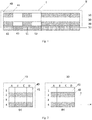
- Fig. 2(a) and Fig. 2(b) are respectively structural schematic diagrams of the first electrode layer 10 and the second electrode layer 30.
- the first electrode layer 10 and the second electrode layer 30 have the same division mode for the electrode units.
- the electrode unit in the first row and A th column in Fig. 2(a) is represented by A1
- the electrode unit in Fig. 2(b) is represented by Al as well in correspondence to the A1 region in Fig. 2(a) .
- the second row and the fourth row of the first electrode layer 10 are composed of the first electrode units 41, and the second row and the fourth row of the second electrode layer 30 are composed of second electrode units 42.
- the rest regions are the openings 43.
- first unit rows and the second unit rows are alternately arranged to form the first electrode layer 10 and the second electrode layer 30 which are composed of the 4 ⁇ 4 electrode units. That is, in the fingerprint identification region I, by regularly removing the electrode units at corresponding positions in the first electrode layer 10 and the second electrode layer 30 every other row, the objective of improving the light transmittance of the first display region I is achieved, and thus the identification sensitivity of the fingerprint module is improved.
- the driver units corresponding to the first units are the third units 51, and the driver units corresponding to the second units are the fourth units 52.
- the third units 51 comprise driver circuits, and the fourth units 52 do not comprise the driver circuits.
- the number of the first unit rows and the number of the second unit rows are not limited to this. That is, the specific numbers may be correspondingly set according to the actual size of the display apparatus and the requirement for the display resolution.
- the shapes of the first electrode units 41 and the shapes of the second electrode units 42 are not limited to this, and may be of any polygons.
- the second electrode layer 30 also may be a continuous film layer having a plurality of the openings 43, or comprises the separated second electrode units 42 prepared on the same layer and having the same shapes.
- part of the driver units corresponding to the first units 41 are the third units 51, and part of the driver units are the fourth units 52 as long as display units capable of emitting lights normally exist in the first display region I.
- the present embodiment provides a display apparatus, as shown in Fig. 3 showing the first display region I.
- the first electrode units 41 in the second row in Fig. 3(a) and the second electrode units 42 in the second row in Fig. 3(b) form intact organic light emitting diode structures.
- the first electrode units 41 in the fourth row in Fig. 3(a) and the second electrode units 42 in the fourth row in Fig. 3(b) form intact organic light emitting diode structures. Only one of the first row in Fig. 3(a) and the first row in Fig. 3(b) has electrode units, and only one of the third row in Fig. 3(a) and the third row in Fig. 3(b) has electrode units, so no lights can be emitted. However, this allows the first display region I has certain light transmittance, so the overall light transmittance of the first display region I is improved.
- all the driver units corresponding to the display units 40 are the third units 51.
- the driver units corresponding to the second units are the fourth units 52, and thus the overall light transmittance of the first display region I may be further improved.
- the present embodiment provides a display apparatus, as shown in Fig. 4 showing the first display region I.
- the first electrode units 41 and the openings 43 in the first electrode layer 10 are alternately arranged, and the second electrode units 42 and the openings 43 in the second electrode layer 30 are alternately arranged.
- the first electrode units 41/second electrode units 42 and the openings 43 are regularly and alternately arranged to form the first electrode layer 10 and the second electrode layer 30 which are composed of 4 ⁇ 4 electrode units. That is, in the first display region I, the electrode units at corresponding positions in the first electrode layer 10 and the second electrode layer 30 are removed every other electrode unit, namely projections of the first electrode layer 10 and the second electrode layer 30 which are subjected to removal of the electrode units in the display layer are completely overlapped in the stacking direction perpendicular to the plane, so the overall light transmittance of the first display region I is improved. In addition, the whole lights of the display apparatus are transmitted more uniformly, so that the processing steps of the subsequent fingerprint identification algorithm may be simplified, and the display units 40 capable of emitting lights independently may be distributed uniformly to achieve relatively high display resolution.
- all the driver units corresponding to the display units 40 are the third units 51.
- the present embodiment provides a display apparatus, as shown in Fig. 5 showing the first display region I.
- the first electrode units 41 and the openings 43 in the first electrode layer 10 are alternately arranged. That is, the first electrode layer 10 is formed by removing the electrode units every other electrode unit, and part of the second electrode units 42 and the openings 43 in the second electrode layer 30 are alternately arranged, and part of the second electrode units 42 or the openings 43 are continuously arranged.
- the second electrode units C4 and D4 in the second electrode layer 30 are continuously arranged, and the rest second electrode units 42 and the openings 43 are alternately arranged.
- the effect of improving the overall light transmittance of the first display region I may be achieved as long as projections of the first electrode layer 10 and the second electrode layer 30, which are subjected to the removal of the electrode units, of the display layer in the stacking direction perpendicular to the plane have overlapped parts.
- all the driver units corresponding to the display units 40 are the third units 51.
- the present embodiment provides a display apparatus. As shown in Fig. 6 , in the first display region I and the second display region II, the first electrode layer 10 and the second electrode layer 30 are overlapped, and each of the display units 40 has an intact organic light emitting diode structure.
- the driver units corresponding to the first display region I, in the driver layer 50 are the third units 51 and the fourth units 52 which are alternately arranged.
- Metal elements lead wires, source and drain electrodes, gate electrodes, capacitance plates and the like) in the driver units have certain light blocking property, part of the driver units in the driver layer 50 are configured as the fourth units 52 not including the driver circuits, and may form light-transmitting regions in the display apparatus.
- the first display region I is a fingerprint identification region, lights for reading a fingerprint are easily emitted from the light-transmitting regions, so that the fingerprint identification sensitivity is high.
- the type of the driver units in the driver layer 50 is not limited as long as at least one of the driver units in the driver layer 50 is the fourth unit 52 to form the light-transmitting region.
Landscapes
- Physics & Mathematics (AREA)
- Engineering & Computer Science (AREA)
- General Physics & Mathematics (AREA)
- Theoretical Computer Science (AREA)
- Computer Hardware Design (AREA)
- Nonlinear Science (AREA)
- Optics & Photonics (AREA)
- Devices For Indicating Variable Information By Combining Individual Elements (AREA)
- Chemical & Material Sciences (AREA)
- Crystallography & Structural Chemistry (AREA)
- Mathematical Physics (AREA)
- Geometry (AREA)
- Microelectronics & Electronic Packaging (AREA)
- Electroluminescent Light Sources (AREA)
- Image Input (AREA)
- Human Computer Interaction (AREA)
- Multimedia (AREA)
Abstract
Description
- The disclosure relates to the field of display technologies, and more particularly to a display apparatus.
- An Organic Light Emitting Diode (OLED) apparatus has the advantages of autoluminescence, low driving voltage, high luminous efficiency, short response time, high definition and contrast, wide viewing, capability of implementing flexible displaying and large-area full-color displaying, etc., Therefore, OLED display technology is considered as a most potential display technology in the industry.
- For an Active Matrix OLED (AMOLED), a thin film transistor cooperates with a capacitor to store signals, so as to control the brightness and the gray-scale performance of the OLED. Each of independent OLEDs is electrically connected with the corresponding thin film transistor to form a pixel matrix. An array circuit formed by the thin film transistors determines luminous conditions of pixels, so as to determine the constitution of an image. The AMOLED generally serves as a large-sized display apparatus thanks to its advantages of size enlargement, power saving, high resolution, relatively long panel life and the like.
- At the present, with the development of the information industry, electronic products have come into an era of intelligence. Due to the uniqueness of a fingerprint pattern, to improve the safety and convenience of use of the electronic products, many electronic products are equipped with a fingerprint pattern identification module to enhance the safety of devices.
- However, due to a large pixel density and a small effective area of light-transmitting holes of pixel units, a high PPI AMOLED screen body having full high definition and above in the prior art causes low overall light transmittance and thus causes the problem of low fingerprint identification sensitivity under optical screen.
- The disclosure aims to overcome a defect of low light transmittance of a fingerprint module of a display apparatus in the prior art.
- In view of the defect, the disclosure provides a display apparatus. The display apparatus comprises a first display region serving as a fingerprint identification region and a second display region serving as a display region. The display apparatus comprises a display layer and a driver layer stacked in a stacking direction perpendicular to a plane where the display apparatus is placed. The display layer comprises a first electrode layer and a second electrode layer stacked in the stacking direction, and the driver layer comprises a plurality of driver units. In the first display region, the first electrode layer has a first part corresponding to the first display region, the second electrode layer has a second part corresponding to the first display region, and a projection of the first part in the stacking direction and a projection of the second part in the stacking direction are not completely overlapped and/or not each of the driver units comprises a driver circuit.
- By partially removing electrodes of the part corresponding to the first electrode layer and/or the part corresponding to the second electrode layer in a display unit in a predetermined region of the display layer and/or by omitting the driver circuits in part of the driver units in the predetermined region, an effect of improving the light transmittance of the predetermined region of the display layer may be achieved.
- Optionally, in the first display region, at least one of the first electrode layer and the second electrode layer has a plurality of openings.
- Optionally, in the first display region, the first electrode layer and the second electrode layer comprises a plurality of electrode units.
- Optionally, the openings are arranged in rows, and the electrode units are arranged in rows; and the rows arranged by the openings are alternate with the rows arranged by the electrode units.
- By removing the first electrode layer and/or the second electrode layer in the display apparatus every other row, when the first display region is a fingerprint identification region, the objective of improving the light transmittance of the fingerprint identification region is achieved, thus increasing the identification rate of the fingerprint module.
- Optionally, the openings are arranged in rows, and the electrode units are arranged in rows. The number of the rows arranged by the openings is less than the number of the rows arranged by the electrode units.
- Optionally, the openings and the electrode units are alternately arranged.
- By removing the first electrode layer and/or the second electrode layer in the first display region in the display apparatus every other electrode unit, when the first display region is the fingerprint identification region, the whole light transmittance of the fingerprint identification region is improved. In addition, lights of the whole display apparatus are transmitted more uniformly, so the subsequent fingerprint identification algorithm is relatively convenient to process.
- Optionally, in the rows arranged by the electrode units, at least two electrode units are continuously arranged, and the rest electrode units and the openings are alternately arranged.
- Optionally, in the stacking direction, a projection of at least one of the electrode units in the first electrode layer is overlapped with a projection of a corresponding number of the electrode units in the second electrode layer.
- Optionally, the display layer further comprises an organic light emitting layer arranged between the first electrode layer and the second electrode layer.
- The display apparatus according to an embodiment of the disclosure achieves the effect of improving the light transmittance of a predetermined region of the display layer.
-
-
Fig. 1 is a structural schematic diagram of a longitudinal cross section of a display apparatus in an embodiment of the disclosure; -
Fig. 2 is a structural schematic diagram of a first electrode layer and a second electrode layer in anEmbodiment 1 of the disclosure; -
Fig. 3 is a structural schematic diagram of a first electrode layer and a second electrode layer in anEmbodiment 2 of the disclosure; -
Fig. 4 is a structural schematic diagram of a first electrode layer and a second electrode layer in anEmbodiment 3 of the disclosure; -
Fig. 5 is a structural schematic diagram of a first electrode layer and a second electrode layer in anEmbodiment 4 of the disclosure; and -
Fig. 6 is a structural schematic diagram of a longitudinal cross section of a display apparatus in an Embodiment 5 of the disclosure. - Numerals in the drawings: I: first display region; II: second display region: 10: first electrode layer; 20: organic light emitting layer; 30: second electrode layer; 40: display unit; 41: first electrode unit; 42: second electrode unit; 43: opening; 50: driver layer; 51: third unit; and 52: fourth unit
- As shown in
Fig. 1 , an embodiment of the disclosure provides a display apparatus, comprising a display layer and adriver layer 50 which are stacked in a stacking direction perpendicular to a plane where the display apparatus is placed. The display layer comprises a plurality ofdisplay units 40 arranged in the same plane. Thedriver layer 50 comprises a plurality of driver units (such as Thin Film Transistors (TFT)) arranged in the same plane. Each of the display units and each of the driver units are in one-to-one correspondence arrangement. - The display layer comprises a
first electrode layer 10, an organiclight emitting layer 20 and asecond electrode layer 30 which are stacked. Thefirst electrode layer 10 comprises a plurality offirst electrode units 41, and thesecond electrode layer 30 comprises a plurality ofsecond electrode units 42. To clearly describe the objectives of the disclosure, in the following descriptions, thefirst electrode layer 10 and thesecond electrode layer 30 are described in detail by taking an electrode layer composed of 4 (the number of rows) × 4 (the number of columns) electrode units for example, and both thefirst electrode layer 10 and thesecond electrode layer 30 are electrode layers made of conductive materials such as metal or metal oxide (such as Indium Tin Oxide (ITO)). However, the protection scope of the disclosure is not limited to these materials. The numbers of the electrode units in thefirst electrode layer 10 and thesecond electrode layer 30 may be specifically set according to an actual situation. That is, the number of rows and the number of columns of the electrode units in thefirst electrode layer 10 and thesecond electrode layer 30 may be equal or not equal, and the materials constituting thefirst electrode layer 10 and thesecond electrode layer 20 may be the same or different. The organiclight emitting layer 20 is divided into a plurality of organic light emitting units by a pixel limiting layer on thefirst electrode layer 10. The organic light emitting units and the corresponding electrode units in thefirst electrode layer 10 and thesecond electrode layer 30 form independent lightemitting display units 40. - In addition, as shown in
Fig. 1 , the display layer comprises a first display region I and a second display region II. In the following descriptions of the disclosure, the first display region I is a fingerprint identification region, and the second display region II is a display region of the display apparatus. However, the protection scope of the disclosure is not limited to this. All measures for implementing the objectives of the disclosure by using the technical solutions (including the first display region I and the second display region II) of the disclosure shall all fall within the protection scope of the disclosure. - In an embodiment of the disclosure, as shown in
Fig. 1 , thedisplay units 40 comprise a plurality of first units and second units. In the following descriptions, each of the first units is an intact organic light emitting diode unit and comprises afirst electrode unit 41, an organic light emitting unit and asecond electrode unit 42 which are stacked, and each of the second units is a non-intact organic light emitting diode unit and comprises an organic light emitting unit or further comprises one of thefirst electrode unit 41 and thesecond electrode unit 42. That is, the second units are located in a region corresponding to the openings of thefirst electrode layer 10 and/or thesecond electrode layer 30. Therefore, it should be understood that, the "display unit" in the disclosure indicates that this unit is a module or unit in the display layer instead of certainly having a display function. Thefirst electrode units 41 and thesecond electrode units 42 are independent quadrangles of the same shapes. The first electrode layer 10 (the second electrode layer 30) is a continuous film layer having a plurality ofopenings 43, or comprises the separated (non-continuous) first electrode units 41 (second electrode units 42) prepared on the same layer and having the same shapes. The first units have the same polygons shapes, and the second units have the same polygons shapes, so as to guarantee regular and uniform distribution of light-transmitting regions, namely lights emitted from the light-transmitting regions are uniformly distributed, which not only simplifies the processing steps of the subsequent fingerprint identification algorithm, but also allows the display apparatus to have relatively high display resolution. - When the first display region I is a fingerprint identification region, and the second display region II is a normal display region, the first display region I comprises the first units and the second units, and the second display region II only comprises the first units, so the light transmittance of the fingerprint identification region is improved without affecting the light transmittance of the second display region II in the display apparatus. However, the protection scope of the disclosure is not limited to this. The second display region II also may comprise both the first units and the second units.
- As shown in
Fig. 1 , the driver units in thedriver layer 50 comprisethird units 51 andfourth units 52. Thethird units 51 comprise driver circuits, and thefourth units 52 do not comprise driver circuits. Therefore, it should be understood that "not each of the driver units comprises a driver circuit for driving each of the display units" or "not each of the driver units comprises a driver circuit" refers to that some of the driver units comprise the driver circuits, and some of the driver units do not comprise the driver circuits. The term "driver unit" in the disclosure indicates that this unit is a module or unit in the driver layer instead of certainly having a driver function. - In addition, technical features involved in different implementation modes of the disclosure described below may be mutually combined as long as they do not constitute conflicts.
- As a metal electrode has certain light blocking property, in the display layer of the first display region I, by removing the electrode units, located in a region corresponding to the
first electrode layer 10 and/or a region corresponding to thesecond electrode layer 30, in thedisplay units 40, namely by forming the second units, the light-transmitting regions may be formed. In addition, thefirst electrode layer 10 and thesecond electrode layer 30, which are subjected to partial removal of the electrode units, in the display layer still have completely overlapped parts in a stacking direction (the up-down direction, hereinafter referred to as "a stacking direction perpendicular to the plane") perpendicular to a plane where the display apparatus (the display unit) is placed, namely they still comprise the first units having the intact organic light emitting diode structures in the first display region I. When the first display region I is a fingerprint identification region, lights for identifying a fingerprint may be emitted from the light-transmitting regions, so that the identification sensitivity is high. Furthermore, the first display region I further comprises the first units having intact organic light emitting diode structures, so as not to affect the display function of the first display region I. - As an embodiment of the disclosure, as shown in
Fig. 2 showing the first display region I, each of thefirst electrode layer 10 and thethird electrode layer 30 comprises electrode units arranged in 4 rows and 4 columns respectively. 1, 2, 3 and 4 in the figure respectively represent the rows of the electrode units, arranged along the y direction, in thefirst electrode layer 10 and thesecond electrode layer 30, and A, B, C and D respectively represent the columns of the electrode units, arranged along the x direction, in thefirst electrode layer 10 and thesecond electrode layer 30.Fig. 2(a) and Fig. 2(b) are respectively structural schematic diagrams of thefirst electrode layer 10 and thesecond electrode layer 30. Thefirst electrode layer 10 and thesecond electrode layer 30 have the same division mode for the electrode units. For example, if the electrode unit in the first row and Ath column inFig. 2(a) is represented by A1, the electrode unit inFig. 2(b) is represented by Al as well in correspondence to the A1 region inFig. 2(a) . - As shown in
Fig. 2 , in the x direction, the second row and the fourth row of thefirst electrode layer 10 are composed of thefirst electrode units 41, and the second row and the fourth row of thesecond electrode layer 30 are composed ofsecond electrode units 42. The rest regions are theopenings 43. - Four continuously arranged
openings 43 are used to constitute a first unit row, and four continuously arrangedfirst electrode units 41/second electrode units 42 are used to constitute a second unit row. Furthermore, the first unit rows and the second unit rows are alternately arranged to form thefirst electrode layer 10 and thesecond electrode layer 30 which are composed of the 4×4 electrode units. That is, in the fingerprint identification region I, by regularly removing the electrode units at corresponding positions in thefirst electrode layer 10 and thesecond electrode layer 30 every other row, the objective of improving the light transmittance of the first display region I is achieved, and thus the identification sensitivity of the fingerprint module is improved. - In the first display region I, as shown in
Fig. 1 , the driver units corresponding to the first units are thethird units 51, and the driver units corresponding to the second units are thefourth units 52. Thethird units 51 comprise driver circuits, and thefourth units 52 do not comprise the driver circuits. By removing the driver circuits, corresponding to the second units (which do not have the intact organic light emitting diode structures), in thedriver layer 50, it can be guaranteed that the lights may be emitted from the light-transmitting regions without obstruction, and the identification sensitivity is high. - As a first replaceable implementation mode of the present embodiment, the number of the first unit rows and the number of the second unit rows are not limited to this. That is, the specific numbers may be correspondingly set according to the actual size of the display apparatus and the requirement for the display resolution.
- As a replaceable implementation mode of the present embodiment, the shapes of the
first electrode units 41 and the shapes of thesecond electrode units 42 are not limited to this, and may be of any polygons. To simplify the process, thesecond electrode layer 30 also may be a continuous film layer having a plurality of theopenings 43, or comprises the separatedsecond electrode units 42 prepared on the same layer and having the same shapes. - As a replaceable implementation mode of the disclosure, in the first display region I, part of the driver units corresponding to the
first units 41 are thethird units 51, and part of the driver units are thefourth units 52 as long as display units capable of emitting lights normally exist in the first display region I. - The present embodiment provides a display apparatus, as shown in
Fig. 3 showing the first display region I. Thefirst electrode units 41 in the second row inFig. 3(a) and thesecond electrode units 42 in the second row inFig. 3(b) form intact organic light emitting diode structures. Thefirst electrode units 41 in the fourth row inFig. 3(a) and thesecond electrode units 42 in the fourth row inFig. 3(b) form intact organic light emitting diode structures. Only one of the first row inFig. 3(a) and the first row inFig. 3(b) has electrode units, and only one of the third row inFig. 3(a) and the third row inFig. 3(b) has electrode units, so no lights can be emitted. However, this allows the first display region I has certain light transmittance, so the overall light transmittance of the first display region I is improved. - As an embodiment of the present disclosure, in the present embodiment, all the driver units corresponding to the
display units 40 are thethird units 51. - As a replaceable implementation mode of the disclosure, the driver units corresponding to the second units are the
fourth units 52, and thus the overall light transmittance of the first display region I may be further improved. - The present embodiment provides a display apparatus, as shown in
Fig. 4 showing the first display region I. In the x direction and the y direction, thefirst electrode units 41 and theopenings 43 in thefirst electrode layer 10 are alternately arranged, and thesecond electrode units 42 and theopenings 43 in thesecond electrode layer 30 are alternately arranged. - The
first electrode units 41/second electrode units 42 and theopenings 43 are regularly and alternately arranged to form thefirst electrode layer 10 and thesecond electrode layer 30 which are composed of 4×4 electrode units. That is, in the first display region I, the electrode units at corresponding positions in thefirst electrode layer 10 and thesecond electrode layer 30 are removed every other electrode unit, namely projections of thefirst electrode layer 10 and thesecond electrode layer 30 which are subjected to removal of the electrode units in the display layer are completely overlapped in the stacking direction perpendicular to the plane, so the overall light transmittance of the first display region I is improved. In addition, the whole lights of the display apparatus are transmitted more uniformly, so that the processing steps of the subsequent fingerprint identification algorithm may be simplified, and thedisplay units 40 capable of emitting lights independently may be distributed uniformly to achieve relatively high display resolution. - As an embodiment of the present embodiment, in the present embodiment, all the driver units corresponding to the
display units 40 are thethird units 51. - The present embodiment provides a display apparatus, as shown in
Fig. 5 showing the first display region I. Thefirst electrode units 41 and theopenings 43 in thefirst electrode layer 10 are alternately arranged. That is, thefirst electrode layer 10 is formed by removing the electrode units every other electrode unit, and part of thesecond electrode units 42 and theopenings 43 in thesecond electrode layer 30 are alternately arranged, and part of thesecond electrode units 42 or theopenings 43 are continuously arranged. For example, as shown inFig. 5(b) , the second electrode units C4 and D4 in thesecond electrode layer 30 are continuously arranged, and the restsecond electrode units 42 and theopenings 43 are alternately arranged. The effect of improving the overall light transmittance of the first display region I may be achieved as long as projections of thefirst electrode layer 10 and thesecond electrode layer 30, which are subjected to the removal of the electrode units, of the display layer in the stacking direction perpendicular to the plane have overlapped parts. - As an embodiment of the present disclosure, in the present embodiment, all the driver units corresponding to the
display units 40 are thethird units 51. - The present embodiment provides a display apparatus. As shown in
Fig. 6 , in the first display region I and the second display region II, thefirst electrode layer 10 and thesecond electrode layer 30 are overlapped, and each of thedisplay units 40 has an intact organic light emitting diode structure. - The driver units, corresponding to the first display region I, in the
driver layer 50 are thethird units 51 and thefourth units 52 which are alternately arranged. Metal elements (lead wires, source and drain electrodes, gate electrodes, capacitance plates and the like) in the driver units have certain light blocking property, part of the driver units in thedriver layer 50 are configured as thefourth units 52 not including the driver circuits, and may form light-transmitting regions in the display apparatus. When the first display region I is a fingerprint identification region, lights for reading a fingerprint are easily emitted from the light-transmitting regions, so that the fingerprint identification sensitivity is high. - As a replaceable implementation mode of the present embodiment, the type of the driver units in the
driver layer 50 is not limited as long as at least one of the driver units in thedriver layer 50 is thefourth unit 52 to form the light-transmitting region. - Obviously, the above-mentioned embodiments are merely examples taken for clear descriptions, but not intended to limit the implementation modes. Those of ordinary skill in the art can further make other changes or modifications in different forms on the basis of the above-mentioned descriptions. Here, it is unnecessary and may not enumerate all implementation modes. Obvious changes or modifications caused therefrom shall still fall within the protection scope of the disclosure.
Claims (9)
- A display apparatus, comprising a first display region serving as a fingerprint identification region and a second display region serving as a display region, and comprising a display layer and a driver layer stacked in a stacking direction perpendicular to a plane where the display apparatus is placed, and the display layer comprising a first electrode layer and a second electrode layer stacked in the stacking direction, and the driver layer comprising a plurality of driver units; and
in the first display region, the first electrode layer having a first part corresponding to the first display region, the second electrode layer having a second part corresponding to the first display region, and a projection of the first part in the stacking direction and a projection of the second part in the stacking direction being not completely overlapped, and/or not each of the driver units comprises a driver circuit. - The display apparatus according to claim 1, characterized in that in the first display region, at least one of the first electrode layer and the second electrode layer has a plurality of openings.
- The display apparatus according to claim 2, characterized in that in the first display region, the first electrode layer and the second electrode layer comprise a plurality of electrode units.
- The display apparatus according to claim 3, characterized in that the openings are arranged in rows, and the electrode units are arranged in rows; and the rows arranged by the openings are alternate with the rows arranged by the electrode units.
- The display apparatus according to claim 3, characterized in that the openings are arranged in rows, and the electrode units are arranged in rows; and the number of the rows arranged by the openings is less than the number of the rows arranged by the electrode units.
- The display apparatus according to claim 3, characterized in that the openings and the electrode units are alternately arranged.
- The display apparatus according to claim 3, characterized in that in the rows arranged by the electrode units, at least two electrode units are continuously arranged, and the rest electrode units and the openings are alternately arranged.
- The display apparatus according to any one of claims 3 to 7, characterized in that in the stacking direction, a projection of at least one of the electrode units in the first electrode layer is overlapped with a projection of a corresponding number of the electrode units in the second electrode layer.
- The display apparatus according to claim 1, characterized in that the display layer further comprises an organic light emitting layer arranged between the first electrode layer and the second electrode layer.
Applications Claiming Priority (2)
| Application Number | Priority Date | Filing Date | Title |
|---|---|---|---|
| CN201721277955.7U CN207517341U (en) | 2017-09-30 | 2017-09-30 | Display device |
| PCT/CN2018/088798 WO2019062176A1 (en) | 2017-09-30 | 2018-05-29 | Display device |
Publications (2)
| Publication Number | Publication Date |
|---|---|
| EP3611718A1 true EP3611718A1 (en) | 2020-02-19 |
| EP3611718A4 EP3611718A4 (en) | 2020-06-24 |
Family
ID=62534248
Family Applications (1)
| Application Number | Title | Priority Date | Filing Date |
|---|---|---|---|
| EP18861187.5A Withdrawn EP3611718A4 (en) | 2017-09-30 | 2018-05-29 | DISPLAY DEVICE |
Country Status (7)
| Country | Link |
|---|---|
| US (1) | US11355562B2 (en) |
| EP (1) | EP3611718A4 (en) |
| JP (1) | JP7026139B2 (en) |
| KR (1) | KR102226567B1 (en) |
| CN (1) | CN207517341U (en) |
| TW (1) | TWM565317U (en) |
| WO (1) | WO2019062176A1 (en) |
Cited By (1)
| Publication number | Priority date | Publication date | Assignee | Title |
|---|---|---|---|---|
| WO2021086511A1 (en) * | 2019-10-29 | 2021-05-06 | Google Llc | Boundary panel layout for artifact compensation in multi-pixel density display panel |
Families Citing this family (13)
| Publication number | Priority date | Publication date | Assignee | Title |
|---|---|---|---|---|
| CN110619813B (en) | 2018-06-20 | 2021-05-14 | 京东方科技集团股份有限公司 | Display substrate, driving method thereof, display device, and high-precision metal mask |
| CN110620129B (en) | 2018-06-20 | 2022-02-01 | 京东方科技集团股份有限公司 | Display substrate, driving method thereof, display device and high-precision metal mask plate |
| US11263968B2 (en) | 2018-06-20 | 2022-03-01 | Boe Technology Group Co., Ltd. | Display substrate and driving method thereof, and display device |
| CN114759073B (en) * | 2018-06-29 | 2025-07-15 | 京东方科技集团股份有限公司 | Display substrate and display device |
| CN110658886A (en) * | 2018-06-29 | 2020-01-07 | 中兴通讯股份有限公司 | Display screen module, terminal, control method and device of terminal, and computer storage medium |
| CN109148537B (en) * | 2018-08-24 | 2021-12-07 | 维沃移动通信有限公司 | Display panel, preparation method and electronic equipment |
| CN109670448B (en) * | 2018-12-20 | 2021-02-23 | 武汉华星光电半导体显示技术有限公司 | Fingerprint identification structure of display screen |
| CN109754710B (en) * | 2019-02-28 | 2021-08-03 | 昆山国显光电有限公司 | Light-shielding layer and display device |
| CN109786432B (en) * | 2019-03-06 | 2021-06-08 | 昆山国显光电有限公司 | Display panel and display device |
| KR20210109709A (en) | 2020-02-27 | 2021-09-07 | 삼성디스플레이 주식회사 | Display device |
| CN111915996B (en) * | 2020-08-10 | 2022-03-08 | 錼创显示科技股份有限公司 | Miniature LED display |
| TWI733551B (en) | 2020-08-10 | 2021-07-11 | 錼創顯示科技股份有限公司 | Micro led display |
| JP2024004358A (en) | 2022-06-28 | 2024-01-16 | 大日本印刷株式会社 | Electronic device and method for manufacturing electronic device |
Family Cites Families (17)
| Publication number | Priority date | Publication date | Assignee | Title |
|---|---|---|---|---|
| KR101287200B1 (en) * | 2005-12-28 | 2013-07-16 | 엘지디스플레이 주식회사 | Flexible Display |
| KR101082224B1 (en) * | 2009-09-08 | 2011-11-09 | 삼성모바일디스플레이주식회사 | liquid crystal display device with a built in touch screen |
| JP5740132B2 (en) * | 2009-10-26 | 2015-06-24 | 株式会社半導体エネルギー研究所 | Display device and semiconductor device |
| KR101900914B1 (en) | 2012-09-18 | 2018-11-05 | 삼성디스플레이 주식회사 | Organic light emitting display device |
| US10460188B2 (en) * | 2014-08-26 | 2019-10-29 | Gingy Technology Inc. | Bio-sensing apparatus |
| KR102265752B1 (en) * | 2014-09-01 | 2021-06-17 | 삼성디스플레이 주식회사 | organic light emitting diode display |
| US10410033B2 (en) | 2015-06-18 | 2019-09-10 | Shenzhen GOODIX Technology Co., Ltd. | Under-LCD screen optical sensor module for on-screen fingerprint sensing |
| CN107004130B (en) | 2015-06-18 | 2020-08-28 | 深圳市汇顶科技股份有限公司 | Optical sensor module under screen for sensing fingerprint on screen |
| US10176355B2 (en) * | 2015-12-03 | 2019-01-08 | Synaptics Incorporated | Optical sensor for integration in a display |
| KR102460544B1 (en) * | 2016-03-09 | 2022-10-31 | 삼성전자주식회사 | Display including sensing function and electronic device having the same |
| EP4246503A3 (en) * | 2016-03-24 | 2023-11-01 | Samsung Electronics Co., Ltd. | Electronic device having display |
| KR20170113066A (en) | 2016-03-24 | 2017-10-12 | 삼성전자주식회사 | Electronic device with display and method for displaying image thereof |
| CN107194321B (en) * | 2017-04-27 | 2020-04-21 | Oppo广东移动通信有限公司 | Display screen, display device and mobile terminal |
| US20180323243A1 (en) * | 2017-05-02 | 2018-11-08 | Boe Technology Group Co., Ltd. | Array substrate, image collection method and display device |
| CN107093617B (en) * | 2017-05-02 | 2019-09-10 | 京东方科技集团股份有限公司 | Array substrate, image-pickup method and display device |
| CN107122750B (en) * | 2017-05-03 | 2020-03-31 | 京东方科技集团股份有限公司 | Optical fingerprint identification device and display panel |
| CN107863370A (en) * | 2017-09-30 | 2018-03-30 | 昆山国显光电有限公司 | Display device |
-
2017
- 2017-09-30 CN CN201721277955.7U patent/CN207517341U/en active Active
-
2018
- 2018-05-29 JP JP2019563401A patent/JP7026139B2/en active Active
- 2018-05-29 WO PCT/CN2018/088798 patent/WO2019062176A1/en not_active Ceased
- 2018-05-29 EP EP18861187.5A patent/EP3611718A4/en not_active Withdrawn
- 2018-05-29 KR KR1020197033177A patent/KR102226567B1/en active Active
- 2018-06-01 TW TW107207358U patent/TWM565317U/en unknown
-
2019
- 2019-10-09 US US16/596,776 patent/US11355562B2/en active Active
Cited By (2)
| Publication number | Priority date | Publication date | Assignee | Title |
|---|---|---|---|---|
| WO2021086511A1 (en) * | 2019-10-29 | 2021-05-06 | Google Llc | Boundary panel layout for artifact compensation in multi-pixel density display panel |
| US11145702B2 (en) | 2019-10-29 | 2021-10-12 | Google Llc | Boundary panel layout for artifact compensation in multi-pixel density display panel |
Also Published As
| Publication number | Publication date |
|---|---|
| KR20190132523A (en) | 2019-11-27 |
| EP3611718A4 (en) | 2020-06-24 |
| US11355562B2 (en) | 2022-06-07 |
| CN207517341U (en) | 2018-06-19 |
| US20200043994A1 (en) | 2020-02-06 |
| JP7026139B2 (en) | 2022-02-25 |
| TWM565317U (en) | 2018-08-11 |
| KR102226567B1 (en) | 2021-03-11 |
| WO2019062176A1 (en) | 2019-04-04 |
| JP2020521999A (en) | 2020-07-27 |
Similar Documents
| Publication | Publication Date | Title |
|---|---|---|
| US11355562B2 (en) | Display apparatus | |
| US11580904B2 (en) | Transparent display panels and display panels | |
| US10871842B2 (en) | Flexible display device, fabrication method and electronic device thereof | |
| US11527558B2 (en) | Display device | |
| US11092863B2 (en) | Storage capacitor, display device using the same and method for manufacturing the same | |
| EP2503536A1 (en) | Active matrix electroluminescent display | |
| US20180197932A1 (en) | Array substrate and display panel | |
| US10971570B2 (en) | Display device and brightness detection method therefor | |
| US20050162079A1 (en) | Display device and manufacturing method thereof | |
| KR20170024197A (en) | Transparent display device | |
| JP6842282B2 (en) | Organic EL display device | |
| CN107577100B (en) | Array substrate, display panel and display device | |
| WO2014205876A1 (en) | Display panel with electrostatic protection function, and electronic device | |
| US12170287B2 (en) | Array substrate, display panel, and display device | |
| US20180083075A1 (en) | Display panel and display apparatus having the display panel | |
| CN110137372B (en) | Display panel and display device | |
| US20230135563A1 (en) | Display device for improving displaying quality and display panel thereof | |
| CN108054187A (en) | Display panel and its bad point processing method, display device | |
| CN109634011B (en) | Array substrate, display panel and display device | |
| US20210335899A1 (en) | Organic light-emitting diode display | |
| US12476226B1 (en) | Display device having light emitting element in concave portion of insulating substrate | |
| KR20240083897A (en) | Display device | |
| US20240186307A1 (en) | Light Emitting Display Device | |
| KR20160074801A (en) | Display panel and organic electroluminescent display appartus having the same | |
| US20250280663A1 (en) | Display Device |
Legal Events
| Date | Code | Title | Description |
|---|---|---|---|
| STAA | Information on the status of an ep patent application or granted ep patent |
Free format text: STATUS: THE INTERNATIONAL PUBLICATION HAS BEEN MADE |
|
| PUAI | Public reference made under article 153(3) epc to a published international application that has entered the european phase |
Free format text: ORIGINAL CODE: 0009012 |
|
| STAA | Information on the status of an ep patent application or granted ep patent |
Free format text: STATUS: REQUEST FOR EXAMINATION WAS MADE |
|
| 17P | Request for examination filed |
Effective date: 20191113 |
|
| AK | Designated contracting states |
Kind code of ref document: A1 Designated state(s): AL AT BE BG CH CY CZ DE DK EE ES FI FR GB GR HR HU IE IS IT LI LT LU LV MC MK MT NL NO PL PT RO RS SE SI SK SM TR |
|
| AX | Request for extension of the european patent |
Extension state: BA ME |
|
| A4 | Supplementary search report drawn up and despatched |
Effective date: 20200525 |
|
| RIC1 | Information provided on ipc code assigned before grant |
Ipc: G09G 3/3225 20160101ALI20200516BHEP Ipc: G09G 3/325 20160101AFI20200516BHEP |
|
| DAV | Request for validation of the european patent (deleted) | ||
| DAX | Request for extension of the european patent (deleted) | ||
| STAA | Information on the status of an ep patent application or granted ep patent |
Free format text: STATUS: EXAMINATION IS IN PROGRESS |
|
| 17Q | First examination report despatched |
Effective date: 20220311 |
|
| STAA | Information on the status of an ep patent application or granted ep patent |
Free format text: STATUS: THE APPLICATION HAS BEEN WITHDRAWN |
|
| 18W | Application withdrawn |
Effective date: 20231109 |