EP3609296A1 - Power supply device - Google Patents
Power supply device Download PDFInfo
- Publication number
- EP3609296A1 EP3609296A1 EP19170877.5A EP19170877A EP3609296A1 EP 3609296 A1 EP3609296 A1 EP 3609296A1 EP 19170877 A EP19170877 A EP 19170877A EP 3609296 A1 EP3609296 A1 EP 3609296A1
- Authority
- EP
- European Patent Office
- Prior art keywords
- power supply
- voltage
- input
- supply device
- circuit
- Prior art date
- Legal status (The legal status is an assumption and is not a legal conclusion. Google has not performed a legal analysis and makes no representation as to the accuracy of the status listed.)
- Granted
Links
Images


Classifications
-
- H—ELECTRICITY
- H05—ELECTRIC TECHNIQUES NOT OTHERWISE PROVIDED FOR
- H05B—ELECTRIC HEATING; ELECTRIC LIGHT SOURCES NOT OTHERWISE PROVIDED FOR; CIRCUIT ARRANGEMENTS FOR ELECTRIC LIGHT SOURCES, IN GENERAL
- H05B45/00—Circuit arrangements for operating light-emitting diodes [LED]
- H05B45/30—Driver circuits
- H05B45/37—Converter circuits
- H05B45/3725—Switched mode power supply [SMPS]
- H05B45/382—Switched mode power supply [SMPS] with galvanic isolation between input and output
-
- H—ELECTRICITY
- H02—GENERATION; CONVERSION OR DISTRIBUTION OF ELECTRIC POWER
- H02M—APPARATUS FOR CONVERSION BETWEEN AC AND AC, BETWEEN AC AND DC, OR BETWEEN DC AND DC, AND FOR USE WITH MAINS OR SIMILAR POWER SUPPLY SYSTEMS; CONVERSION OF DC OR AC INPUT POWER INTO SURGE OUTPUT POWER; CONTROL OR REGULATION THEREOF
- H02M1/00—Details of apparatus for conversion
-
- H—ELECTRICITY
- H05—ELECTRIC TECHNIQUES NOT OTHERWISE PROVIDED FOR
- H05B—ELECTRIC HEATING; ELECTRIC LIGHT SOURCES NOT OTHERWISE PROVIDED FOR; CIRCUIT ARRANGEMENTS FOR ELECTRIC LIGHT SOURCES, IN GENERAL
- H05B45/00—Circuit arrangements for operating light-emitting diodes [LED]
- H05B45/40—Details of LED load circuits
- H05B45/44—Details of LED load circuits with an active control inside an LED matrix
-
- H—ELECTRICITY
- H05—ELECTRIC TECHNIQUES NOT OTHERWISE PROVIDED FOR
- H05B—ELECTRIC HEATING; ELECTRIC LIGHT SOURCES NOT OTHERWISE PROVIDED FOR; CIRCUIT ARRANGEMENTS FOR ELECTRIC LIGHT SOURCES, IN GENERAL
- H05B45/00—Circuit arrangements for operating light-emitting diodes [LED]
- H05B45/30—Driver circuits
- H05B45/37—Converter circuits
-
- H—ELECTRICITY
- H02—GENERATION; CONVERSION OR DISTRIBUTION OF ELECTRIC POWER
- H02M—APPARATUS FOR CONVERSION BETWEEN AC AND AC, BETWEEN AC AND DC, OR BETWEEN DC AND DC, AND FOR USE WITH MAINS OR SIMILAR POWER SUPPLY SYSTEMS; CONVERSION OF DC OR AC INPUT POWER INTO SURGE OUTPUT POWER; CONTROL OR REGULATION THEREOF
- H02M3/00—Conversion of DC power input into DC power output
- H02M3/22—Conversion of DC power input into DC power output with intermediate conversion into AC
- H02M3/24—Conversion of DC power input into DC power output with intermediate conversion into AC by static converters
- H02M3/28—Conversion of DC power input into DC power output with intermediate conversion into AC by static converters using discharge tubes with control electrode or semiconductor devices with control electrode to produce the intermediate AC
- H02M3/325—Conversion of DC power input into DC power output with intermediate conversion into AC by static converters using discharge tubes with control electrode or semiconductor devices with control electrode to produce the intermediate AC using devices of a triode or a transistor type requiring continuous application of a control signal
- H02M3/335—Conversion of DC power input into DC power output with intermediate conversion into AC by static converters using discharge tubes with control electrode or semiconductor devices with control electrode to produce the intermediate AC using devices of a triode or a transistor type requiring continuous application of a control signal using semiconductor devices only
- H02M3/33507—Conversion of DC power input into DC power output with intermediate conversion into AC by static converters using discharge tubes with control electrode or semiconductor devices with control electrode to produce the intermediate AC using devices of a triode or a transistor type requiring continuous application of a control signal using semiconductor devices only with automatic control of the output voltage or current, e.g. flyback converters
- H02M3/33523—Conversion of DC power input into DC power output with intermediate conversion into AC by static converters using discharge tubes with control electrode or semiconductor devices with control electrode to produce the intermediate AC using devices of a triode or a transistor type requiring continuous application of a control signal using semiconductor devices only with automatic control of the output voltage or current, e.g. flyback converters with galvanic isolation between input and output of both the power stage and the feedback loop
-
- H—ELECTRICITY
- H05—ELECTRIC TECHNIQUES NOT OTHERWISE PROVIDED FOR
- H05B—ELECTRIC HEATING; ELECTRIC LIGHT SOURCES NOT OTHERWISE PROVIDED FOR; CIRCUIT ARRANGEMENTS FOR ELECTRIC LIGHT SOURCES, IN GENERAL
- H05B45/00—Circuit arrangements for operating light-emitting diodes [LED]
- H05B45/40—Details of LED load circuits
-
- H—ELECTRICITY
- H05—ELECTRIC TECHNIQUES NOT OTHERWISE PROVIDED FOR
- H05B—ELECTRIC HEATING; ELECTRIC LIGHT SOURCES NOT OTHERWISE PROVIDED FOR; CIRCUIT ARRANGEMENTS FOR ELECTRIC LIGHT SOURCES, IN GENERAL
- H05B45/00—Circuit arrangements for operating light-emitting diodes [LED]
- H05B45/50—Circuit arrangements for operating light-emitting diodes [LED] responsive to malfunctions or undesirable behaviour of LEDs; responsive to LED life; Protective circuits
Definitions
- the present invention relates to a power supply device.
- Japanese Patent Laying-Open No. 2006-349626 discloses an implementation circuit that can detect a drop in supply of power-supply voltage.
- the implementation circuit includes an LED device for monitoring the status of the power-supply voltage, and a lighting control circuit for the LED device.
- the lighting control circuit turns on the LED device.
- the lighting control circuit turns off the LED device.
- the power supply device can notify the user of whether or not a voltage is being inputted to the power supply device.
- the user cannot know the magnitude of voltage inputted to the power supply device.
- interconnections for different power-supply voltages may be laid. If a power supply device meant for a certain power-supply line (e.g. a line for AC of 230 V) is connected to a power-supply line for a lower voltage (e.g. a line for AC of 115 V), the output or efficiency of the power supply device may reduce.
- a power supply device meant for a certain power-supply line e.g. a line for AC of 230 V
- a power-supply line for a lower voltage e.g. a line for AC of 115 V
- An object of the present invention is to provide a power supply device that enables the user to easily check the magnitude of the input voltage.
- a power supply device includes: an input unit configured to receive an input voltage from outside; a power supply unit configured to generate a power-supply voltage from the input voltage inputted through the input unit; an output unit including an output terminal configured to output the power-supply voltage; and a lighting circuit connected to the input unit and configured to be turned on in response to application of the input voltage.
- the lighting circuit is configured to vary in lighting mode depending on the input voltage.
- a power supply device that enables the user to easily check the magnitude of the input voltage can be provided. Further, the power supply device requires no circuit for measuring the input voltage value. Thus, the configuration of the power supply device can be simplified, and an increase in cost of the power supply device can be curbed.
- the lighting circuit includes a plurality of light-emitting devices, and the number of light-emitting devices to be turned on among the plurality of light-emitting devices is varied depending on the magnitude of the input voltage.
- the magnitude of the input voltage can be indicated by the number of light-emitting devices to be turned on.
- the lighting circuit further includes a plurality of Zener diodes each connected to a high-voltage side of a corresponding one of the plurality of light-emitting devices, and the plurality of Zener diodes are connected in series.
- the number of light-emitting devices to be turned on can be varied depending on the magnitude of the input voltage.
- Fig. 1 is a block diagram showing one configuration example of a power supply device 100 according to an embodiment.
- power supply device 100 is, for example, a switching power supply device.
- Power supply device 100 includes an input unit 10 to receive an input voltage from outside, a power supply unit 20, and an output unit 30.
- input unit 10 is connected to an AC power supply (e.g. a commercial power supply with 50 Hz / 60 Hz, 100 V / 200 V) 1.
- Input unit 10 includes input terminals 14, 15 (also denoted by "INPUT"), a fuse 11 which is a protective circuit connected to input terminal 14, and a protective earth terminal 16.
- Power supply unit 20 generates a power-supply voltage from the voltage inputted through input unit 10.
- power supply unit 20 includes a rectifier circuit 21, a transformer 22, a MOSFET 23 as a switching device, and a rectifying-smoothing circuit 24.
- power supply unit 20 includes a rush current limiting circuit 25, a noise filter 26, a smoothing circuit 27, a drive control circuit 28, an overcurrent detection circuit 29, a voltage detection circuit 41, an overvoltage detection circuit 42, a photo coupler 43, a photo coupler 44, and capacitors 45, 46.
- Rush current limiting circuit 25 comprises, for example, a resistor and a relay inserted in parallel with the resistor.
- the relay opens to prevent a rush current for several tens of milliseconds from a start-up. After that, the relay closes and power supply device 100 starts up.
- Noise filter 26 filters out a high-frequency noise component superimposed on the AC voltage inputted to INPUT, and supplies rectifier circuit 21 with the AC voltage including no noise component.
- Smoothing circuit 27 comprises a smoothing capacitor to smooth the voltage after full-wave rectification.
- Transformer 22 includes a primary winding 22p, a secondary winding 22s, and an auxiliary winding 22a. Transformer 22 induces a high-frequency pulse voltage generated in primary winding 22p into secondary winding 22s and auxiliary winding 22a. The high-frequency pulse voltage induced into secondary winding 22s is used for DC output. The high-frequency pulse voltage induced into auxiliary winding 22a is used for start-up of drive control circuit 28.
- Rectifying-smoothing circuit 24 comprises a rectifier circuit and a smoothing capacitor. Rectifying-smoothing circuit 24 rectifies and smoothes the high-frequency pulsed power supply (AC power supply) induced into secondary winding 22s of transformer 22, and generates a DC output having a predetermined output voltage and output current.
- AC power supply high-frequency pulsed power supply
- Voltage detection circuit 41 detects the output voltage of the DC output power supply as a corresponding step-down voltage.
- Photo coupler 43 outputs, to drive control circuit 28, a signal corresponding to the detected step-down voltage.
- Overvoltage detection circuit 42 detects an overvoltage when the output voltage of the DC output power supply exceeds a predetermined voltage.
- Photo coupler 44 outputs, to drive control circuit 28, a signal representing the detection of an overvoltage.
- Drive control circuit 28 comprises a control IC including, for example, a pulse width modulation (PWM) signal generator, a feedback control circuit, an over current protection (OCP) terminal, a switching drive terminal, and a drive power terminal.
- PWM pulse width modulation
- OCP over current protection
- Drive control circuit 28 drives MOSFET 23 by supplying the PWM signal to the gate of MOSFET 23.
- the secondary-side voltage detected by voltage detection circuit 41 is fed back to drive control circuit 28 via photo coupler 43.
- Drive control circuit 28 changes the duty cycle of the PWM signal based on this voltage, and drives MOSFET 23 so that the power-supply voltage (output voltage) will be a predetermined voltage.
- MOSFET 23 is connected in series with primary winding 22p of transformer 22. MOSFET 23 turns on and off the primary-side voltage in response to the PWM signal supplied from drive control circuit 28, and generates a high-frequency pulsed power supply at primary winding 22p of transformer 22.
- Output unit 30 includes output terminals 32, 33.
- the power-supply voltage generated in power supply unit 20 is outputted from output terminals 32, 33 (also denoted by "DC OUTPUT").
- DC OUTPUT also denoted by "DC OUTPUT"
- a DC voltage is outputted as the power-supply voltage.
- Power supply device 100 further includes an LED circuit 12, an LED circuit 13, and an LED circuit 31, as lighting circuits.
- Each of LED circuits 12, 13, and 31 includes an LED (light-emitting device).
- LED circuit 12 is connected to input terminal 14 and is turned on in response to application of an input voltage to input terminal 14.
- LED circuit 13 is disposed between fuse 11 and power supply unit 20 and is turned on in response to input of a voltage to power supply unit 20 through fuse 11.
- LED circuit 31 is connected to output terminals 32, 33 and is turned on in response to an output from power supply unit 20.
- Fig. 2 shows lighting patterns of the LED circuits according to one embodiment.
- "input 1", “input 2”, and “output 1” respectively represent LED circuit 12, LED circuit 13, and LED circuit 31.
- Fig. 2 describes all possible lighting patterns.
- Pattern 1 is a pattern in which all of input 1, input 2, and output 1 are ON. Pattern 1 indicates that power supply device 100 is operating normally. The internal state of power supply device 100 is a normal state.
- Pattern 2 is a pattern in which input 1 and input 2 are ON, and output 1 is OFF. Pattern 2 indicates the presence of an abnormality on the secondary side of power supply unit 20 (the abnormality may be, for example, a short circuit on the output side or breakage on the secondary side).
- Pattern 3 is a pattern in which input 1 and output 1 are ON, and input 2 is OFF. However, it is impossible for power supply device 100 to have an internal state corresponding to this pattern.
- Pattern 4 is a pattern in which input 1 is ON, and input 2 and output 1 are OFF. Pattern 4 indicates the presence of an abnormality, such as melt of fuse 11 or breakage on the primary side of power supply unit 20.
- Pattern 5 is a pattern in which input 1 is OFF, and input 2 and output 1 are ON. Pattern 5 indicates that power supply device 100 is in the state of a holding time. However, the state may not actually occur.
- Pattern 6 is a pattern in which input 1 and output 1 are OFF, and input 2 is ON. However, it is impossible for power supply device 100 to have an internal state corresponding to this pattern.
- Pattern 7 is a pattern in which input 1 and input 2 are OFF, and output 1 is ON. This state may occur when a voltage is applied from outside of power supply device 100, for example.
- Pattern 8 is a pattern in which all of input 1, input 2, and output 1 are OFF, with no input voltage.
- the lighting mode of LED circuit 12 is varied depending on the input voltage of power supply device 100.
- the lighting mode of LED circuit 12 is varied depending on the input voltage of power supply device 100. This enables the user to check whether or not an intended input voltage is being applied to power supply device 100.
- a power supply device that enables the user to easily check the level of input voltage can be provided.
- Fig. 3 is a circuit diagram showing a configuration example of LED circuit 12 (lighting circuit) shown in Fig. 1 .
- LED circuit 12 includes a diode 50, Zener diodes 51, 52, 53, 54, resistors 61, 62, 63, 64, and LEDs 71, 72, 73, 74.
- Zener diodes 51, 52, 53, 54 are respectively connected to LEDs 71, 72, 73, 74, on their high-voltage side (anode side). Further, Zener diodes 51, 52, 53, 54 are connected in series.
- diode 50, Zener diode 51, resistor 61, and LED 71 are connected in series.
- Zener diode 52, resistor 62, and LED 72 are connected in series; and the cathode of Zener diode 52 is connected to the anode of Zener diode 51.
- Zener diode 53, resistor 63, and LED 73 are connected in series; and the cathode of Zener diode 53 is connected to the anode of Zener diode 52.
- Zener diode 54, resistor 64, and LED 74 are connected in series; and the cathode of Zener diode 54 is connected to the anode of Zener diode 53.
- the number of LEDs to be turned on can be varied depending on the input voltage. Specifically, as the input voltage increases, the number of LEDs to be turned on increases. In a first range of the input voltage, LED 71 is ON. In a second range of the input voltage, LEDs 71, 72 are ON. In a third range of the input voltage, LEDs 71, 72, 73 are ON. In a fourth range of the input voltage, LEDs 71, 72, 73, 74 are ON.
- Zener voltages Vz Zener voltages Vz
- the lighting of LEDs 71 to 74 can be synchronized with the input of the power supply device. Accordingly, when an instantaneous voltage drop occurs in the input power source for example, the number of lighted LEDs is decreased, thus enabling the user to know the occurrence of the instantaneous voltage drop.
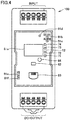
- Fig. 4 schematically shows one example external appearance of power supply device 100 according to an embodiment of the present invention.
- display circuits 81a to 81f on the face of power supply device 100 where INPUT terminals and DC-OUTPUT terminals are disposed, display circuits 81a to 81f, LED circuit 12 (LEDs 71 to 74), a display switching/resetting key 82, a communication port 83, and an output voltage adjusting trimmer 84 are placed.
- the layout shown in Fig. 4 is by way of example.
- Display circuit 81a comprises, for example, a seven-segment LED.
- Display circuit 81a may be an LCD, an organic electroluminescent display, or the like.
- display circuit 81a displays an output voltage, an output current, a lifespan before replacement, a total operating time, and the like.
- LED circuit 12 varies the number of LEDs to be turned on depending on the magnitude of the input voltage.
- Each of display circuits 81b, 81c, 81d includes an LED.
- the LED of display circuit 81d when an input voltage is normally inputted to power supply unit 20 of power supply device 100, the LED of display circuit 81d is ON.
- the LED of display circuit 81b When a DC voltage is outputted from power supply device 100, the LED of display circuit 81b is ON.
- the LED of display circuit 81c is ON.
- Display circuit 81d and display circuit 81b are implementations of LED circuit 12 and LED circuit 31, respectively, shown in Fig. 1 , for example.
- Display circuit 81e and display circuit 81f include LEDs. The lighting of the LEDs indicates the communication status of communication port 83.
- Display switching/resetting key 82 is operated to switch the parameters to be displayed. Also, display switching/resetting key 82 is operated to reset the communication settings. Output voltage adjusting trimmer 84 is operated to adjust the output voltage.
- the power supply device shown in Fig. 4 is disposed on a control board at a manufacturing location, for example. At a manufacturing location, interconnections (power-supply lines) for different power-supply voltages may be laid. If a power supply device meant for a certain power-supply line (e.g. a line for AC of 230 V) is connected to a power-supply line for a lower voltage (e.g. a line for AC of 115 V), the output or efficiency of the power supply device may reduce.
- a certain power-supply line e.g. a line for AC of 230 V
- a lower voltage e.g. a line for AC of 115 V
- the lighting mode of LED circuit 12 is varied depending on the magnitude of the input voltage. Specifically, the number of LEDs to be turned on is varied depending on the magnitude of the input voltage. Thus, the user can check whether or not an intended input voltage is being applied to power supply device 100. Also, a change in the number of lighted LEDs enables the user to know a change in input voltage level. Thus, when an instantaneous drop in input voltage of power supply device 100 occurs for example, the user can know the occurrence of the instantaneous voltage drop.
- the power supply device uses a plurality of LEDs to indicate the range of the input voltage.
- another lighting mode of LED may be employed.
- the emission color of an LED(s) may be varied depending on the range of the input voltage.
- the present embodiment includes the following disclosure.
- a power supply device (100) comprising:
- the power supply device (100) according to configuration 1, wherein the lighting circuit (12) includes a plurality of light-emitting devices (71 to 74), and the number of light-emitting devices to be turned on among the plurality of light-emitting devices (71 to 74) is varied depending on the magnitude of the input voltage.
Landscapes
- Engineering & Computer Science (AREA)
- Power Engineering (AREA)
- Circuit Arrangement For Electric Light Sources In General (AREA)
- Dc-Dc Converters (AREA)
Abstract
Description
- The present invention relates to a power supply device.
- For example, Japanese Patent Laying-Open No.
2006-349626 - According to the above-described configuration, the power supply device can notify the user of whether or not a voltage is being inputted to the power supply device. The user, however, cannot know the magnitude of voltage inputted to the power supply device.
- At a manufacturing location, for example, interconnections (a plurality of power-supply lines) for different power-supply voltages may be laid. If a power supply device meant for a certain power-supply line (e.g. a line for AC of 230 V) is connected to a power-supply line for a lower voltage (e.g. a line for AC of 115 V), the output or efficiency of the power supply device may reduce.
- An object of the present invention is to provide a power supply device that enables the user to easily check the magnitude of the input voltage.
- According to one example of the present disclosure, a power supply device includes: an input unit configured to receive an input voltage from outside; a power supply unit configured to generate a power-supply voltage from the input voltage inputted through the input unit; an output unit including an output terminal configured to output the power-supply voltage; and a lighting circuit connected to the input unit and configured to be turned on in response to application of the input voltage. The lighting circuit is configured to vary in lighting mode depending on the input voltage.
- According to the above-described configuration, a power supply device that enables the user to easily check the magnitude of the input voltage can be provided. Further, the power supply device requires no circuit for measuring the input voltage value. Thus, the configuration of the power supply device can be simplified, and an increase in cost of the power supply device can be curbed.
- In the above-described power supply device, the lighting circuit includes a plurality of light-emitting devices, and the number of light-emitting devices to be turned on among the plurality of light-emitting devices is varied depending on the magnitude of the input voltage.
- According to the above-described configuration, the magnitude of the input voltage can be indicated by the number of light-emitting devices to be turned on.
- In the above-described power supply device, the lighting circuit further includes a plurality of Zener diodes each connected to a high-voltage side of a corresponding one of the plurality of light-emitting devices, and the plurality of Zener diodes are connected in series.
- According to the above-described configuration, the number of light-emitting devices to be turned on can be varied depending on the magnitude of the input voltage.
- The foregoing and other objects, features, aspects and advantages of the present invention will become more apparent from the following detailed description of the present invention when taken in conjunction with the accompanying drawings.
-
-
Fig. 1 is a block diagram showing one configuration example of a power supply device according to an embodiment. -
Fig. 2 shows lighting patterns of LED circuits according to one embodiment. -
Fig. 3 is a circuit diagram showing a configuration example of an LED circuit (lighting circuit) shown inFig. 1 . -
Fig. 4 schematically shows one example external appearance of a power supply device according to an embodiment of the present invention. - An embodiment is hereinafter described in detail with reference to the drawings. In the drawings, identical reference numerals or characters denote identical or corresponding parts.
- First of all, one example situation to which the present invention is applicable is described with reference to
Fig. 1. Fig. 1 is a block diagram showing one configuration example of apower supply device 100 according to an embodiment. As shown inFig. 1 ,power supply device 100 is, for example, a switching power supply device.Power supply device 100 includes aninput unit 10 to receive an input voltage from outside, apower supply unit 20, and anoutput unit 30. - For example,
input unit 10 is connected to an AC power supply (e.g. a commercial power supply with 50 Hz / 60 Hz, 100 V / 200 V) 1.Input unit 10 includesinput terminals 14, 15 (also denoted by "INPUT"), afuse 11 which is a protective circuit connected toinput terminal 14, and aprotective earth terminal 16. -
Power supply unit 20 generates a power-supply voltage from the voltage inputted throughinput unit 10. As an example,power supply unit 20 includes arectifier circuit 21, atransformer 22, aMOSFET 23 as a switching device, and a rectifying-smoothing circuit 24. Further,power supply unit 20 includes a rush current limitingcircuit 25, anoise filter 26, asmoothing circuit 27, adrive control circuit 28, anovercurrent detection circuit 29, avoltage detection circuit 41, anovervoltage detection circuit 42, aphoto coupler 43, aphoto coupler 44, andcapacitors - Rush current limiting
circuit 25 comprises, for example, a resistor and a relay inserted in parallel with the resistor. The relay opens to prevent a rush current for several tens of milliseconds from a start-up. After that, the relay closes andpower supply device 100 starts up. -
Noise filter 26 filters out a high-frequency noise component superimposed on the AC voltage inputted to INPUT, and suppliesrectifier circuit 21 with the AC voltage including no noise component.Smoothing circuit 27 comprises a smoothing capacitor to smooth the voltage after full-wave rectification. - Transformer 22 includes a
primary winding 22p, asecondary winding 22s, and anauxiliary winding 22a.Transformer 22 induces a high-frequency pulse voltage generated in primary winding 22p intosecondary winding 22s andauxiliary winding 22a. The high-frequency pulse voltage induced intosecondary winding 22s is used for DC output. The high-frequency pulse voltage induced intoauxiliary winding 22a is used for start-up ofdrive control circuit 28. - Rectifying-
smoothing circuit 24 comprises a rectifier circuit and a smoothing capacitor. Rectifying-smoothing circuit 24 rectifies and smoothes the high-frequency pulsed power supply (AC power supply) induced intosecondary winding 22s oftransformer 22, and generates a DC output having a predetermined output voltage and output current. -
Voltage detection circuit 41 detects the output voltage of the DC output power supply as a corresponding step-down voltage.Photo coupler 43 outputs, to drivecontrol circuit 28, a signal corresponding to the detected step-down voltage.Overvoltage detection circuit 42 detects an overvoltage when the output voltage of the DC output power supply exceeds a predetermined voltage.Photo coupler 44 outputs, to drivecontrol circuit 28, a signal representing the detection of an overvoltage. -
Drive control circuit 28 comprises a control IC including, for example, a pulse width modulation (PWM) signal generator, a feedback control circuit, an over current protection (OCP) terminal, a switching drive terminal, and a drive power terminal.Drive control circuit 28 drivesMOSFET 23 by supplying the PWM signal to the gate ofMOSFET 23. - The secondary-side voltage detected by
voltage detection circuit 41 is fed back to drivecontrol circuit 28 viaphoto coupler 43.Drive control circuit 28 changes the duty cycle of the PWM signal based on this voltage, and drivesMOSFET 23 so that the power-supply voltage (output voltage) will be a predetermined voltage. -
MOSFET 23 is connected in series withprimary winding 22p oftransformer 22.MOSFET 23 turns on and off the primary-side voltage in response to the PWM signal supplied fromdrive control circuit 28, and generates a high-frequency pulsed power supply at primary winding 22p oftransformer 22. -
Output unit 30 includesoutput terminals power supply unit 20 is outputted fromoutput terminals 32, 33 (also denoted by "DC OUTPUT"). In the configuration shown inFig. 1 , a DC voltage is outputted as the power-supply voltage. -
Power supply device 100 further includes anLED circuit 12, anLED circuit 13, and anLED circuit 31, as lighting circuits. Each ofLED circuits LED circuit 12 is connected to input terminal 14 and is turned on in response to application of an input voltage to input terminal 14.LED circuit 13 is disposed betweenfuse 11 andpower supply unit 20 and is turned on in response to input of a voltage topower supply unit 20 throughfuse 11.LED circuit 31 is connected tooutput terminals power supply unit 20. -
Fig. 2 shows lighting patterns of the LED circuits according to one embodiment. InFig. 2 , "input 1", "input 2", and "output 1" respectively representLED circuit 12,LED circuit 13, andLED circuit 31. Each ofLED circuits Fig. 2 describes all possible lighting patterns. -
Pattern 1 is a pattern in which all ofinput 1,input 2, andoutput 1 are ON.Pattern 1 indicates thatpower supply device 100 is operating normally. The internal state ofpower supply device 100 is a normal state. -
Pattern 2 is a pattern in whichinput 1 andinput 2 are ON, andoutput 1 is OFF.Pattern 2 indicates the presence of an abnormality on the secondary side of power supply unit 20 (the abnormality may be, for example, a short circuit on the output side or breakage on the secondary side). -
Pattern 3 is a pattern in whichinput 1 andoutput 1 are ON, andinput 2 is OFF. However, it is impossible forpower supply device 100 to have an internal state corresponding to this pattern. -
Pattern 4 is a pattern in whichinput 1 is ON, andinput 2 andoutput 1 are OFF.Pattern 4 indicates the presence of an abnormality, such as melt offuse 11 or breakage on the primary side ofpower supply unit 20. -
Pattern 5 is a pattern in whichinput 1 is OFF, andinput 2 andoutput 1 are ON.Pattern 5 indicates thatpower supply device 100 is in the state of a holding time. However, the state may not actually occur. -
Pattern 6 is a pattern in whichinput 1 andoutput 1 are OFF, andinput 2 is ON. However, it is impossible forpower supply device 100 to have an internal state corresponding to this pattern. -
Pattern 7 is a pattern in whichinput 1 andinput 2 are OFF, andoutput 1 is ON. This state may occur when a voltage is applied from outside ofpower supply device 100, for example. -
Pattern 8 is a pattern in which all ofinput 1,input 2, andoutput 1 are OFF, with no input voltage. - In an embodiment, the lighting mode of
LED circuit 12 is varied depending on the input voltage ofpower supply device 100. Thus, inpatterns 1 to 4 shown inFig. 2 (i.e., the patterns in which "input 1" is ON), the lighting mode ofLED circuit 12 is varied depending on the input voltage ofpower supply device 100. This enables the user to check whether or not an intended input voltage is being applied topower supply device 100. Thus, a power supply device that enables the user to easily check the level of input voltage can be provided. -
Fig. 3 is a circuit diagram showing a configuration example of LED circuit 12 (lighting circuit) shown inFig. 1 . With reference toFig. 3 ,LED circuit 12 includes adiode 50,Zener diodes resistors LEDs -
Zener diodes LEDs Zener diodes - Specifically,
diode 50,Zener diode 51,resistor 61, andLED 71 are connected in series.Zener diode 52,resistor 62, andLED 72 are connected in series; and the cathode ofZener diode 52 is connected to the anode ofZener diode 51. Similarly,Zener diode 53,resistor 63, andLED 73 are connected in series; and the cathode ofZener diode 53 is connected to the anode ofZener diode 52.Zener diode 54,resistor 64, andLED 74 are connected in series; and the cathode ofZener diode 54 is connected to the anode ofZener diode 53. - According to this circuit, the number of LEDs to be turned on can be varied depending on the input voltage. Specifically, as the input voltage increases, the number of LEDs to be turned on increases. In a first range of the input voltage,
LED 71 is ON. In a second range of the input voltage,LEDs LEDs LEDs Zener diodes LED circuit 12 can be adjusted so thatLEDs - With the above-described configuration, the lighting of
LEDs 71 to 74 can be synchronized with the input of the power supply device. Accordingly, when an instantaneous voltage drop occurs in the input power source for example, the number of lighted LEDs is decreased, thus enabling the user to know the occurrence of the instantaneous voltage drop. -
Fig. 4 schematically shows one example external appearance ofpower supply device 100 according to an embodiment of the present invention. As shown inFig. 4 , on the face ofpower supply device 100 where INPUT terminals and DC-OUTPUT terminals are disposed,display circuits 81a to 81f, LED circuit 12 (LEDs 71 to 74), a display switching/resettingkey 82, acommunication port 83, and an outputvoltage adjusting trimmer 84 are placed. The layout shown inFig. 4 is by way of example. -
Display circuit 81a comprises, for example, a seven-segment LED.Display circuit 81a may be an LCD, an organic electroluminescent display, or the like. For example,display circuit 81a displays an output voltage, an output current, a lifespan before replacement, a total operating time, and the like. -
LED circuit 12 varies the number of LEDs to be turned on depending on the magnitude of the input voltage. - Each of
display circuits power supply unit 20 ofpower supply device 100, the LED ofdisplay circuit 81d is ON. When a DC voltage is outputted frompower supply device 100, the LED ofdisplay circuit 81b is ON. On the other hand, when an abnormality occurs inpower supply device 100, the LED ofdisplay circuit 81c is ON.Display circuit 81d anddisplay circuit 81b are implementations ofLED circuit 12 andLED circuit 31, respectively, shown inFig. 1 , for example. -
Display circuit 81e and display circuit 81f include LEDs. The lighting of the LEDs indicates the communication status ofcommunication port 83. - Display switching/resetting
key 82 is operated to switch the parameters to be displayed. Also, display switching/resettingkey 82 is operated to reset the communication settings. Outputvoltage adjusting trimmer 84 is operated to adjust the output voltage. - The power supply device shown in
Fig. 4 is disposed on a control board at a manufacturing location, for example. At a manufacturing location, interconnections (power-supply lines) for different power-supply voltages may be laid. If a power supply device meant for a certain power-supply line (e.g. a line for AC of 230 V) is connected to a power-supply line for a lower voltage (e.g. a line for AC of 115 V), the output or efficiency of the power supply device may reduce. - In the present embodiment, the lighting mode of
LED circuit 12 is varied depending on the magnitude of the input voltage. Specifically, the number of LEDs to be turned on is varied depending on the magnitude of the input voltage. Thus, the user can check whether or not an intended input voltage is being applied topower supply device 100. Also, a change in the number of lighted LEDs enables the user to know a change in input voltage level. Thus, when an instantaneous drop in input voltage ofpower supply device 100 occurs for example, the user can know the occurrence of the instantaneous voltage drop. - In the above-described embodiment, the power supply device uses a plurality of LEDs to indicate the range of the input voltage. However, in the present embodiment, another lighting mode of LED may be employed. For example, the emission color of an LED(s) may be varied depending on the range of the input voltage.
- As described above, the present embodiment includes the following disclosure.
- A power supply device (100) comprising:
- an input unit (10) configured to receive an input voltage from outside;
- a power supply unit (20) configured to generate a power-supply voltage from the input voltage inputted through the input unit (10);
- an output unit (30) including an output terminal (32, 33) configured to output the power-supply voltage; and
- a lighting circuit (12) connected to the input unit (10) and configured to be turned on in response to application of the input voltage,
- the lighting circuit (12) being configured to vary in lighting mode depending on the input voltage.
- The power supply device (100) according to
configuration 1, wherein
the lighting circuit (12) includes a plurality of light-emitting devices (71 to 74), and
the number of light-emitting devices to be turned on among the plurality of light-emitting devices (71 to 74) is varied depending on the magnitude of the input voltage. - The power supply device (100) according to
configuration 2, wherein
the lighting circuit (12) further includes a plurality of Zener diodes (51 to 54) each connected to a high-voltage side of a corresponding one of the plurality of light-emitting devices (71 to 74), and
the plurality of Zener diodes (51 to 54) are connected in series. - It should be understood that the embodiment disclosed herein is by way of example in every respect and without limitation. The scope of the present invention is defined by the terms of the claims, and is intended to include any modification within the meaning and scope equivalent to the terms of the claims.
Claims (3)
- A power supply device (100) comprising:an input unit (10) configured to receive an input voltage from outside;a power supply unit (20) configured to generate a power-supply voltage from the input voltage inputted through the input unit (10);an output unit (30) including an output terminal (32, 33) configured to output the power-supply voltage; anda lighting circuit (12) connected to the input unit (10) and configured to be turned on in response to application of the input voltage,the lighting circuit (12) being configured to vary in lighting mode depending on the input voltage.
- The power supply device (100) according to claim 1, wherein
the lighting circuit (12) includes a plurality of light-emitting devices (71 to 74), and
the number of light-emitting devices to be turned on among the plurality of light-emitting devices (71 to 74) is varied depending on the magnitude of the input voltage. - The power supply device (100) according to claim 2, wherein
the lighting circuit (12) further includes a plurality of Zener diodes (51 to 54) each connected to a high-voltage side of a corresponding one of the plurality of light-emitting devices (71 to 74), and
the plurality of Zener diodes (51 to 54) are connected in series.
Applications Claiming Priority (1)
| Application Number | Priority Date | Filing Date | Title |
|---|---|---|---|
| JP2018148426A JP7035894B2 (en) | 2018-08-07 | 2018-08-07 | Power supply |
Publications (2)
| Publication Number | Publication Date |
|---|---|
| EP3609296A1 true EP3609296A1 (en) | 2020-02-12 |
| EP3609296B1 EP3609296B1 (en) | 2021-12-01 |
Family
ID=66251702
Family Applications (1)
| Application Number | Title | Priority Date | Filing Date |
|---|---|---|---|
| EP19170877.5A Not-in-force EP3609296B1 (en) | 2018-08-07 | 2019-04-24 | Power supply device |
Country Status (5)
| Country | Link |
|---|---|
| US (1) | US11006497B2 (en) |
| EP (1) | EP3609296B1 (en) |
| JP (1) | JP7035894B2 (en) |
| KR (1) | KR102291763B1 (en) |
| CN (1) | CN110831274B (en) |
Families Citing this family (4)
| Publication number | Priority date | Publication date | Assignee | Title |
|---|---|---|---|---|
| JP2019103299A (en) * | 2017-12-05 | 2019-06-24 | オムロン株式会社 | Power supply device |
| KR102682617B1 (en) * | 2021-08-18 | 2024-07-05 | 임행삼 | LED lighting apparatuses |
| CN114285017B (en) * | 2021-12-29 | 2024-01-30 | 北京动力源科技股份有限公司 | Switch power supply |
| TWI844370B (en) * | 2023-05-22 | 2024-06-01 | 宏碁股份有限公司 | Power supply device supporting power delivery |
Citations (4)
| Publication number | Priority date | Publication date | Assignee | Title |
|---|---|---|---|---|
| US20020047593A1 (en) * | 2000-09-29 | 2002-04-25 | Guthrie Don W. | Enhanced trim resolution voltage-controlled dimming led driver |
| JP2006349626A (en) | 2005-06-20 | 2006-12-28 | Noritsu Koki Co Ltd | Mounting circuit with voltage confirmation LED |
| DE102005053298A1 (en) * | 2005-11-09 | 2007-05-16 | Kromberg & Schubert Gmbh & Co | Lighting device for motor vehicle, has light emitting diodes that are connected in series-and parallel switch, and bypass switch that provides current flow through functional light emitting diode during failure of light emitting diodes |
| WO2016202665A1 (en) * | 2015-06-19 | 2016-12-22 | Philips Lighting Holding B.V. | Led arrangement and led driving method |
Family Cites Families (23)
| Publication number | Priority date | Publication date | Assignee | Title |
|---|---|---|---|---|
| JPS5120528A (en) * | 1974-08-09 | 1976-02-18 | Toko Inc | Chokuryu chokuryuhenkanki |
| US4307606A (en) * | 1979-06-11 | 1981-12-29 | Johnson Hugh G | Thermal transition zone sensing and indicating system |
| US4716301A (en) * | 1986-04-08 | 1987-12-29 | Chamberlain Manufacturing Corporation | Digital light control |
| JP3010605B2 (en) * | 1991-11-20 | 2000-02-21 | 富士電機株式会社 | Switching power supply |
| KR100335190B1 (en) * | 1997-03-27 | 2002-11-13 | 기아자동차주식회사 | Control relay for certifying disorder |
| US7358679B2 (en) * | 2002-05-09 | 2008-04-15 | Philips Solid-State Lighting Solutions, Inc. | Dimmable LED-based MR16 lighting apparatus and methods |
| US6944034B1 (en) * | 2003-06-30 | 2005-09-13 | Iwatt Inc. | System and method for input current shaping in a power converter |
| JP2005151674A (en) * | 2003-11-14 | 2005-06-09 | Omron Corp | Power supply |
| US20110062888A1 (en) * | 2004-12-01 | 2011-03-17 | Bondy Montgomery C | Energy saving extra-low voltage dimmer and security lighting system wherein fixture control is local to the illuminated area |
| US7397194B2 (en) * | 2005-07-11 | 2008-07-08 | Varon Lighting, Inc. | Auxiliary quartz lamp lighting system for high intensity discharge lamp ballasts |
| JP3749912B1 (en) * | 2005-09-01 | 2006-03-01 | 日本▲まき▼線工業株式会社 | Portable transformer |
| JP2007109483A (en) * | 2005-10-12 | 2007-04-26 | Chugoku Electric Power Co Inc:The | Voltage indicator |
| TWI580305B (en) * | 2008-09-05 | 2017-04-21 | 艾杜雷控股有限公司 | Led based lighting application |
| US7902761B2 (en) * | 2008-10-03 | 2011-03-08 | Next Gen Illumination, Inc | Dimmable LED lamp |
| CN102022702A (en) * | 2009-09-11 | 2011-04-20 | 展晶科技(深圳)有限公司 | Protective circuit of luminescence module, light emitting diode wafer and alternating current light emitting diode |
| JP2011158350A (en) * | 2010-02-01 | 2011-08-18 | Tomofumi Fukuda | Operating state visual observation simple device by current detection |
| US8680784B2 (en) * | 2010-06-15 | 2014-03-25 | Maxim Integrated Products, Inc. | Dimmable offline LED driver |
| JP5586385B2 (en) * | 2010-09-08 | 2014-09-10 | 三菱電機株式会社 | Self-excited light emitting device and self-excited sterilization device |
| TWI535331B (en) * | 2011-01-31 | 2016-05-21 | Midas Wei Trading Co Ltd | Light emitting diode protection circuit |
| WO2012158383A2 (en) * | 2011-05-13 | 2012-11-22 | Lutron Electronics Co., Inc. | Control device having a night light |
| JP5342626B2 (en) | 2011-09-27 | 2013-11-13 | シャープ株式会社 | LED drive circuit and LED illumination lamp using the same |
| JP5794113B2 (en) * | 2011-11-04 | 2015-10-14 | オムロン株式会社 | Solid state relay and load drive circuit |
| CN106097986A (en) | 2016-08-23 | 2016-11-09 | 深圳市华星光电技术有限公司 | A kind of backlight drive circuit |
-
2018
- 2018-08-07 JP JP2018148426A patent/JP7035894B2/en active Active
-
2019
- 2019-04-18 KR KR1020190045426A patent/KR102291763B1/en active Active
- 2019-04-24 EP EP19170877.5A patent/EP3609296B1/en not_active Not-in-force
- 2019-04-24 US US16/392,682 patent/US11006497B2/en active Active
- 2019-04-25 CN CN201910339283.5A patent/CN110831274B/en not_active Expired - Fee Related
Patent Citations (4)
| Publication number | Priority date | Publication date | Assignee | Title |
|---|---|---|---|---|
| US20020047593A1 (en) * | 2000-09-29 | 2002-04-25 | Guthrie Don W. | Enhanced trim resolution voltage-controlled dimming led driver |
| JP2006349626A (en) | 2005-06-20 | 2006-12-28 | Noritsu Koki Co Ltd | Mounting circuit with voltage confirmation LED |
| DE102005053298A1 (en) * | 2005-11-09 | 2007-05-16 | Kromberg & Schubert Gmbh & Co | Lighting device for motor vehicle, has light emitting diodes that are connected in series-and parallel switch, and bypass switch that provides current flow through functional light emitting diode during failure of light emitting diodes |
| WO2016202665A1 (en) * | 2015-06-19 | 2016-12-22 | Philips Lighting Holding B.V. | Led arrangement and led driving method |
Also Published As
| Publication number | Publication date |
|---|---|
| KR102291763B1 (en) | 2021-08-23 |
| CN110831274A (en) | 2020-02-21 |
| US20200053846A1 (en) | 2020-02-13 |
| CN110831274B (en) | 2021-09-17 |
| EP3609296B1 (en) | 2021-12-01 |
| JP7035894B2 (en) | 2022-03-15 |
| KR20200016780A (en) | 2020-02-17 |
| US11006497B2 (en) | 2021-05-11 |
| JP2020025395A (en) | 2020-02-13 |
Similar Documents
| Publication | Publication Date | Title |
|---|---|---|
| EP3609296B1 (en) | Power supply device | |
| EP2063522A2 (en) | Switching power supply device | |
| KR20130056012A (en) | Switching mode power supply having overvoltage cut-off function, image forming apparatus and method for overvoltage cut-off by using the same | |
| CN101373925B (en) | Power supply apparatus | |
| EP1494342A2 (en) | An under-Voltage detection circuit | |
| JP2008048515A (en) | Switching power supply | |
| US8836236B1 (en) | LED offset voltage dimmer | |
| US11057974B2 (en) | Power supply device | |
| KR101553219B1 (en) | Apparatus of driving led | |
| JP2017158244A (en) | Power supply apparatus | |
| JP7014137B2 (en) | Power supply | |
| KR100855871B1 (en) | Rechargeable Power Supply and Control Method | |
| KR20140011242A (en) | Power supply circuit | |
| US8723436B2 (en) | LED lighting device and illumination apparatus including same | |
| KR20060035028A (en) | Single signal lamp with remaining time indication and power supply used therein | |
| WO2012023635A1 (en) | Light-emitting diode driver for phase control | |
| KR19990005543U (en) | Overload Protection Circuit of Power Supply | |
| US20190342972A1 (en) | Light source power supply | |
| KR20110023248A (en) | Display device | |
| KR20070054355A (en) | Power circuit | |
| JP2005285422A (en) | Guide light | |
| KR20000015611A (en) | Circuit for protecting excessive voltage of a monitor | |
| KR20000011742U (en) | Switching Mode Power Supplies | |
| JP2018063899A (en) | Lighting device | |
| KR20000014585U (en) | The output voltage stabilization circuit of the switching power supply circuit |
Legal Events
| Date | Code | Title | Description |
|---|---|---|---|
| PUAI | Public reference made under article 153(3) epc to a published international application that has entered the european phase |
Free format text: ORIGINAL CODE: 0009012 |
|
| STAA | Information on the status of an ep patent application or granted ep patent |
Free format text: STATUS: REQUEST FOR EXAMINATION WAS MADE |
|
| 17P | Request for examination filed |
Effective date: 20190424 |
|
| AK | Designated contracting states |
Kind code of ref document: A1 Designated state(s): AL AT BE BG CH CY CZ DE DK EE ES FI FR GB GR HR HU IE IS IT LI LT LU LV MC MK MT NL NO PL PT RO RS SE SI SK SM TR |
|
| AX | Request for extension of the european patent |
Extension state: BA ME |
|
| STAA | Information on the status of an ep patent application or granted ep patent |
Free format text: STATUS: EXAMINATION IS IN PROGRESS |
|
| 17Q | First examination report despatched |
Effective date: 20200721 |
|
| REG | Reference to a national code |
Ref country code: DE Ref legal event code: R079 Ref document number: 602019009620 Country of ref document: DE Free format text: PREVIOUS MAIN CLASS: H05B0033080000 Ipc: H05B0045370000 |
|
| RIC1 | Information provided on ipc code assigned before grant |
Ipc: H05B 45/44 20200101ALI20210806BHEP Ipc: H05B 45/37 20200101AFI20210806BHEP |
|
| GRAP | Despatch of communication of intention to grant a patent |
Free format text: ORIGINAL CODE: EPIDOSNIGR1 |
|
| STAA | Information on the status of an ep patent application or granted ep patent |
Free format text: STATUS: GRANT OF PATENT IS INTENDED |
|
| GRAS | Grant fee paid |
Free format text: ORIGINAL CODE: EPIDOSNIGR3 |
|
| GRAA | (expected) grant |
Free format text: ORIGINAL CODE: 0009210 |
|
| STAA | Information on the status of an ep patent application or granted ep patent |
Free format text: STATUS: THE PATENT HAS BEEN GRANTED |
|
| INTG | Intention to grant announced |
Effective date: 20211005 |
|
| RIN1 | Information on inventor provided before grant (corrected) |
Inventor name: NAGANO, MASAAKI |
|
| AK | Designated contracting states |
Kind code of ref document: B1 Designated state(s): AL AT BE BG CH CY CZ DE DK EE ES FI FR GB GR HR HU IE IS IT LI LT LU LV MC MK MT NL NO PL PT RO RS SE SI SK SM TR |
|
| REG | Reference to a national code |
Ref country code: GB Ref legal event code: FG4D |
|
| REG | Reference to a national code |
Ref country code: AT Ref legal event code: REF Ref document number: 1453002 Country of ref document: AT Kind code of ref document: T Effective date: 20211215 Ref country code: CH Ref legal event code: EP |
|
| REG | Reference to a national code |
Ref country code: IE Ref legal event code: FG4D |
|
| REG | Reference to a national code |
Ref country code: DE Ref legal event code: R096 Ref document number: 602019009620 Country of ref document: DE |
|
| REG | Reference to a national code |
Ref country code: LT Ref legal event code: MG9D |
|
| REG | Reference to a national code |
Ref country code: NL Ref legal event code: MP Effective date: 20211201 |
|
| REG | Reference to a national code |
Ref country code: AT Ref legal event code: MK05 Ref document number: 1453002 Country of ref document: AT Kind code of ref document: T Effective date: 20211201 |
|
| PG25 | Lapsed in a contracting state [announced via postgrant information from national office to epo] |
Ref country code: RS Free format text: LAPSE BECAUSE OF FAILURE TO SUBMIT A TRANSLATION OF THE DESCRIPTION OR TO PAY THE FEE WITHIN THE PRESCRIBED TIME-LIMIT Effective date: 20211201 Ref country code: LT Free format text: LAPSE BECAUSE OF FAILURE TO SUBMIT A TRANSLATION OF THE DESCRIPTION OR TO PAY THE FEE WITHIN THE PRESCRIBED TIME-LIMIT Effective date: 20211201 Ref country code: FI Free format text: LAPSE BECAUSE OF FAILURE TO SUBMIT A TRANSLATION OF THE DESCRIPTION OR TO PAY THE FEE WITHIN THE PRESCRIBED TIME-LIMIT Effective date: 20211201 Ref country code: BG Free format text: LAPSE BECAUSE OF FAILURE TO SUBMIT A TRANSLATION OF THE DESCRIPTION OR TO PAY THE FEE WITHIN THE PRESCRIBED TIME-LIMIT Effective date: 20220301 Ref country code: AT Free format text: LAPSE BECAUSE OF FAILURE TO SUBMIT A TRANSLATION OF THE DESCRIPTION OR TO PAY THE FEE WITHIN THE PRESCRIBED TIME-LIMIT Effective date: 20211201 |
|
| PG25 | Lapsed in a contracting state [announced via postgrant information from national office to epo] |
Ref country code: SE Free format text: LAPSE BECAUSE OF FAILURE TO SUBMIT A TRANSLATION OF THE DESCRIPTION OR TO PAY THE FEE WITHIN THE PRESCRIBED TIME-LIMIT Effective date: 20211201 Ref country code: PL Free format text: LAPSE BECAUSE OF FAILURE TO SUBMIT A TRANSLATION OF THE DESCRIPTION OR TO PAY THE FEE WITHIN THE PRESCRIBED TIME-LIMIT Effective date: 20211201 Ref country code: NO Free format text: LAPSE BECAUSE OF FAILURE TO SUBMIT A TRANSLATION OF THE DESCRIPTION OR TO PAY THE FEE WITHIN THE PRESCRIBED TIME-LIMIT Effective date: 20220301 Ref country code: LV Free format text: LAPSE BECAUSE OF FAILURE TO SUBMIT A TRANSLATION OF THE DESCRIPTION OR TO PAY THE FEE WITHIN THE PRESCRIBED TIME-LIMIT Effective date: 20211201 Ref country code: HR Free format text: LAPSE BECAUSE OF FAILURE TO SUBMIT A TRANSLATION OF THE DESCRIPTION OR TO PAY THE FEE WITHIN THE PRESCRIBED TIME-LIMIT Effective date: 20211201 Ref country code: GR Free format text: LAPSE BECAUSE OF FAILURE TO SUBMIT A TRANSLATION OF THE DESCRIPTION OR TO PAY THE FEE WITHIN THE PRESCRIBED TIME-LIMIT Effective date: 20220302 Ref country code: ES Free format text: LAPSE BECAUSE OF FAILURE TO SUBMIT A TRANSLATION OF THE DESCRIPTION OR TO PAY THE FEE WITHIN THE PRESCRIBED TIME-LIMIT Effective date: 20211201 |
|
| PG25 | Lapsed in a contracting state [announced via postgrant information from national office to epo] |
Ref country code: NL Free format text: LAPSE BECAUSE OF FAILURE TO SUBMIT A TRANSLATION OF THE DESCRIPTION OR TO PAY THE FEE WITHIN THE PRESCRIBED TIME-LIMIT Effective date: 20211201 |
|
| PG25 | Lapsed in a contracting state [announced via postgrant information from national office to epo] |
Ref country code: SM Free format text: LAPSE BECAUSE OF FAILURE TO SUBMIT A TRANSLATION OF THE DESCRIPTION OR TO PAY THE FEE WITHIN THE PRESCRIBED TIME-LIMIT Effective date: 20211201 Ref country code: SK Free format text: LAPSE BECAUSE OF FAILURE TO SUBMIT A TRANSLATION OF THE DESCRIPTION OR TO PAY THE FEE WITHIN THE PRESCRIBED TIME-LIMIT Effective date: 20211201 Ref country code: RO Free format text: LAPSE BECAUSE OF FAILURE TO SUBMIT A TRANSLATION OF THE DESCRIPTION OR TO PAY THE FEE WITHIN THE PRESCRIBED TIME-LIMIT Effective date: 20211201 Ref country code: PT Free format text: LAPSE BECAUSE OF FAILURE TO SUBMIT A TRANSLATION OF THE DESCRIPTION OR TO PAY THE FEE WITHIN THE PRESCRIBED TIME-LIMIT Effective date: 20220401 Ref country code: EE Free format text: LAPSE BECAUSE OF FAILURE TO SUBMIT A TRANSLATION OF THE DESCRIPTION OR TO PAY THE FEE WITHIN THE PRESCRIBED TIME-LIMIT Effective date: 20211201 Ref country code: CZ Free format text: LAPSE BECAUSE OF FAILURE TO SUBMIT A TRANSLATION OF THE DESCRIPTION OR TO PAY THE FEE WITHIN THE PRESCRIBED TIME-LIMIT Effective date: 20211201 |
|
| REG | Reference to a national code |
Ref country code: DE Ref legal event code: R097 Ref document number: 602019009620 Country of ref document: DE |
|
| PG25 | Lapsed in a contracting state [announced via postgrant information from national office to epo] |
Ref country code: IS Free format text: LAPSE BECAUSE OF FAILURE TO SUBMIT A TRANSLATION OF THE DESCRIPTION OR TO PAY THE FEE WITHIN THE PRESCRIBED TIME-LIMIT Effective date: 20220401 |
|
| PLBE | No opposition filed within time limit |
Free format text: ORIGINAL CODE: 0009261 |
|
| STAA | Information on the status of an ep patent application or granted ep patent |
Free format text: STATUS: NO OPPOSITION FILED WITHIN TIME LIMIT |
|
| PG25 | Lapsed in a contracting state [announced via postgrant information from national office to epo] |
Ref country code: DK Free format text: LAPSE BECAUSE OF FAILURE TO SUBMIT A TRANSLATION OF THE DESCRIPTION OR TO PAY THE FEE WITHIN THE PRESCRIBED TIME-LIMIT Effective date: 20211201 Ref country code: AL Free format text: LAPSE BECAUSE OF FAILURE TO SUBMIT A TRANSLATION OF THE DESCRIPTION OR TO PAY THE FEE WITHIN THE PRESCRIBED TIME-LIMIT Effective date: 20211201 |
|
| 26N | No opposition filed |
Effective date: 20220902 |
|
| PG25 | Lapsed in a contracting state [announced via postgrant information from national office to epo] |
Ref country code: SI Free format text: LAPSE BECAUSE OF FAILURE TO SUBMIT A TRANSLATION OF THE DESCRIPTION OR TO PAY THE FEE WITHIN THE PRESCRIBED TIME-LIMIT Effective date: 20211201 |
|
| REG | Reference to a national code |
Ref country code: CH Ref legal event code: PL |
|
| REG | Reference to a national code |
Ref country code: BE Ref legal event code: MM Effective date: 20220430 |
|
| PG25 | Lapsed in a contracting state [announced via postgrant information from national office to epo] |
Ref country code: MC Free format text: LAPSE BECAUSE OF FAILURE TO SUBMIT A TRANSLATION OF THE DESCRIPTION OR TO PAY THE FEE WITHIN THE PRESCRIBED TIME-LIMIT Effective date: 20211201 Ref country code: LU Free format text: LAPSE BECAUSE OF NON-PAYMENT OF DUE FEES Effective date: 20220424 Ref country code: LI Free format text: LAPSE BECAUSE OF NON-PAYMENT OF DUE FEES Effective date: 20220430 Ref country code: FR Free format text: LAPSE BECAUSE OF NON-PAYMENT OF DUE FEES Effective date: 20220430 Ref country code: CH Free format text: LAPSE BECAUSE OF NON-PAYMENT OF DUE FEES Effective date: 20220430 |
|
| PG25 | Lapsed in a contracting state [announced via postgrant information from national office to epo] |
Ref country code: BE Free format text: LAPSE BECAUSE OF NON-PAYMENT OF DUE FEES Effective date: 20220430 |
|
| PG25 | Lapsed in a contracting state [announced via postgrant information from national office to epo] |
Ref country code: IE Free format text: LAPSE BECAUSE OF NON-PAYMENT OF DUE FEES Effective date: 20220424 |
|
| PG25 | Lapsed in a contracting state [announced via postgrant information from national office to epo] |
Ref country code: IT Free format text: LAPSE BECAUSE OF FAILURE TO SUBMIT A TRANSLATION OF THE DESCRIPTION OR TO PAY THE FEE WITHIN THE PRESCRIBED TIME-LIMIT Effective date: 20211201 |
|
| PGFP | Annual fee paid to national office [announced via postgrant information from national office to epo] |
Ref country code: DE Payment date: 20230228 Year of fee payment: 5 |
|
| GBPC | Gb: european patent ceased through non-payment of renewal fee |
Effective date: 20230424 |
|
| PG25 | Lapsed in a contracting state [announced via postgrant information from national office to epo] |
Ref country code: GB Free format text: LAPSE BECAUSE OF NON-PAYMENT OF DUE FEES Effective date: 20230424 |
|
| PG25 | Lapsed in a contracting state [announced via postgrant information from national office to epo] |
Ref country code: GB Free format text: LAPSE BECAUSE OF NON-PAYMENT OF DUE FEES Effective date: 20230424 |
|
| PG25 | Lapsed in a contracting state [announced via postgrant information from national office to epo] |
Ref country code: MK Free format text: LAPSE BECAUSE OF FAILURE TO SUBMIT A TRANSLATION OF THE DESCRIPTION OR TO PAY THE FEE WITHIN THE PRESCRIBED TIME-LIMIT Effective date: 20211201 Ref country code: CY Free format text: LAPSE BECAUSE OF FAILURE TO SUBMIT A TRANSLATION OF THE DESCRIPTION OR TO PAY THE FEE WITHIN THE PRESCRIBED TIME-LIMIT Effective date: 20211201 |
|
| PG25 | Lapsed in a contracting state [announced via postgrant information from national office to epo] |
Ref country code: HU Free format text: LAPSE BECAUSE OF FAILURE TO SUBMIT A TRANSLATION OF THE DESCRIPTION OR TO PAY THE FEE WITHIN THE PRESCRIBED TIME-LIMIT; INVALID AB INITIO Effective date: 20190424 |
|
| PG25 | Lapsed in a contracting state [announced via postgrant information from national office to epo] |
Ref country code: MT Free format text: LAPSE BECAUSE OF FAILURE TO SUBMIT A TRANSLATION OF THE DESCRIPTION OR TO PAY THE FEE WITHIN THE PRESCRIBED TIME-LIMIT Effective date: 20211201 |
|
| REG | Reference to a national code |
Ref country code: DE Ref legal event code: R119 Ref document number: 602019009620 Country of ref document: DE |
|
| PG25 | Lapsed in a contracting state [announced via postgrant information from national office to epo] |
Ref country code: DE Free format text: LAPSE BECAUSE OF NON-PAYMENT OF DUE FEES Effective date: 20241105 |
|
| PG25 | Lapsed in a contracting state [announced via postgrant information from national office to epo] |
Ref country code: DE Free format text: LAPSE BECAUSE OF NON-PAYMENT OF DUE FEES Effective date: 20241105 |
|
| PG25 | Lapsed in a contracting state [announced via postgrant information from national office to epo] |
Ref country code: TR Free format text: LAPSE BECAUSE OF FAILURE TO SUBMIT A TRANSLATION OF THE DESCRIPTION OR TO PAY THE FEE WITHIN THE PRESCRIBED TIME-LIMIT Effective date: 20211201 |