EP3608837A1 - Display screen, electronic device and method for three-dimensional feature recognition - Google Patents
Display screen, electronic device and method for three-dimensional feature recognition Download PDFInfo
- Publication number
- EP3608837A1 EP3608837A1 EP19190662.7A EP19190662A EP3608837A1 EP 3608837 A1 EP3608837 A1 EP 3608837A1 EP 19190662 A EP19190662 A EP 19190662A EP 3608837 A1 EP3608837 A1 EP 3608837A1
- Authority
- EP
- European Patent Office
- Prior art keywords
- area
- target
- display screen
- light spots
- target object
- Prior art date
- Legal status (The legal status is an assumption and is not a legal conclusion. Google has not performed a legal analysis and makes no representation as to the accuracy of the status listed.)
- Withdrawn
Links
Images



Classifications
-
- G—PHYSICS
- G06—COMPUTING OR CALCULATING; COUNTING
- G06V—IMAGE OR VIDEO RECOGNITION OR UNDERSTANDING
- G06V40/00—Recognition of biometric, human-related or animal-related patterns in image or video data
- G06V40/10—Human or animal bodies, e.g. vehicle occupants or pedestrians; Body parts, e.g. hands
- G06V40/16—Human faces, e.g. facial parts, sketches or expressions
- G06V40/161—Detection; Localisation; Normalisation
- G06V40/166—Detection; Localisation; Normalisation using acquisition arrangements
-
- H—ELECTRICITY
- H10—SEMICONDUCTOR DEVICES; ELECTRIC SOLID-STATE DEVICES NOT OTHERWISE PROVIDED FOR
- H10F—INORGANIC SEMICONDUCTOR DEVICES SENSITIVE TO INFRARED RADIATION, LIGHT, ELECTROMAGNETIC RADIATION OF SHORTER WAVELENGTH OR CORPUSCULAR RADIATION
- H10F39/00—Integrated devices, or assemblies of multiple devices, comprising at least one element covered by group H10F30/00, e.g. radiation detectors comprising photodiode arrays
- H10F39/10—Integrated devices
- H10F39/12—Image sensors
- H10F39/18—Complementary metal-oxide-semiconductor [CMOS] image sensors; Photodiode array image sensors
- H10F39/184—Infrared image sensors
-
- G—PHYSICS
- G06—COMPUTING OR CALCULATING; COUNTING
- G06T—IMAGE DATA PROCESSING OR GENERATION, IN GENERAL
- G06T7/00—Image analysis
- G06T7/70—Determining position or orientation of objects or cameras
- G06T7/73—Determining position or orientation of objects or cameras using feature-based methods
-
- G—PHYSICS
- G06—COMPUTING OR CALCULATING; COUNTING
- G06V—IMAGE OR VIDEO RECOGNITION OR UNDERSTANDING
- G06V40/00—Recognition of biometric, human-related or animal-related patterns in image or video data
- G06V40/10—Human or animal bodies, e.g. vehicle occupants or pedestrians; Body parts, e.g. hands
- G06V40/16—Human faces, e.g. facial parts, sketches or expressions
- G06V40/172—Classification, e.g. identification
-
- G—PHYSICS
- G06—COMPUTING OR CALCULATING; COUNTING
- G06T—IMAGE DATA PROCESSING OR GENERATION, IN GENERAL
- G06T2207/00—Indexing scheme for image analysis or image enhancement
- G06T2207/10—Image acquisition modality
- G06T2207/10028—Range image; Depth image; 3D point clouds
-
- G—PHYSICS
- G06—COMPUTING OR CALCULATING; COUNTING
- G06T—IMAGE DATA PROCESSING OR GENERATION, IN GENERAL
- G06T2207/00—Indexing scheme for image analysis or image enhancement
- G06T2207/30—Subject of image; Context of image processing
- G06T2207/30196—Human being; Person
- G06T2207/30201—Face
-
- G—PHYSICS
- G09—EDUCATION; CRYPTOGRAPHY; DISPLAY; ADVERTISING; SEALS
- G09G—ARRANGEMENTS OR CIRCUITS FOR CONTROL OF INDICATING DEVICES USING STATIC MEANS TO PRESENT VARIABLE INFORMATION
- G09G2360/00—Aspects of the architecture of display systems
- G09G2360/14—Detecting light within display terminals, e.g. using a single or a plurality of photosensors
Definitions
- the present disclosure relates to the field of electronic technology, and more particularly to a display screen, an electronic device and a method for three-dimensional feature recognition.
- identification components such as an infrared emitter and an infrared camera for performing three-dimensional (3D) feature (such as 3D face feature) recognition generally need to be disposed outside an display area of an electronic device, so that a non-display area needs to be reserved to dispose these components, which limited a further increasing of the display area.
- 3D three-dimensional
- the technical problem to be solved in the present disclosure is to provide a display screen, an electronic device and a method for 3D feature recognition, which can increase a screen-to-body ratio.
- a display screen includes a plurality of display units distributed in an array across a display area of the display screen, a plurality of infrared emitting elements embedded in a first area of the display area, and a plurality of photosensitive elements embedded in a second area of the display area of the display screen.
- the plurality of infrared emitting elements is configured to emit infrared light for illuminating a target object in front of the display screen so as to form a plurality of light spots on the target object.
- the plurality of photosensitive elements is configured to receive target light spots reflected from the target object and convert the target light spots into photo-electrical signals suitable for generating a target image of the target object.
- an electronic device in another aspect of the present disclosure, includes a display screen and a processor.
- the display screen includes a plurality of display units distributed in an array across a display area of the display screen, a plurality of infrared emitting elements embedded in a first area of the display area, and a plurality of photosensitive elements embedded in a second area of the display area.
- the plurality of infrared emitting elements is configured to emit infrared light for illuminating a target object in front of the display screen so as to form a plurality of light spots on the target object.
- the plurality of photosensitive elements is configured to receive target light spots reflected from the target object and convert the target light spots into photo-electrical signals.
- the processor is electrically connected to the plurality of photosensitive elements, and configured to perform an image processing operation to obtain a target image according to the photo-electrical signals generated by the plurality of photosensitive elements, and to identify one or more 3D features of the target object according to the target image.
- a 3D feature recognition method includes emitting infrared light by a plurality of infrared emitting elements of a display screen to illuminate a target object in front of the display screen so as to form a plurality of light spots on the target object, receiving, by a plurality of photosensitive elements of the display screen, target light spots reflected from the target object, converting the target light spots into photo-electrical signals by the plurality of photosensitive elements, performing an image processing operation to obtain a target image according to the photo-electrical signals generated by the plurality of photosensitive elements, and identifying one or more 3D features of the target object according to the target image.
- a 3D feature recognition assembly such as the plurality of infrared emitting elements and the plurality of photosensitive elements, is embedded in the display area of the display.
- FIG. 1 is a schematic structural diagram illustrating a display screen 1 according to an embodiment of the present disclosure.
- the display screen 1 includes a display area A0.
- a plurality of display units 11 is distributed in an array throughout the display area A0 of the display screen 1.
- a plurality of infrared emitting elements 12 is embedded in a first area A1 of the display area A0 of the display screen 1
- a plurality of photosensitive elements 13 is embedded in a second area A2 of the display area A0 of the display screen 1.
- the plurality of photosensitive elements 13 is combined into an image sensor.
- the plurality of infrared emitting elements 12 is configured to emit infrared light for illuminating a target object in front of the display screen 1, such that a plurality of light spots is formed on the target object.
- the plurality of photosensitive elements 13 is configured to receive target light spots reflected from the target object in response to the plurality of light spots and convert the target light spots into photo-electrical signals suitable for generating a target image for identifying 3D feature of the target object.
- the target light spots may include a plurality of reflecting light spots reflected by the target object in response to the plurality of light spots.
- a 3D feature recognition assembly such as the plurality of infrared emitting elements 12 and the plurality of photosensitive elements 13, is embedded in the display area A0 of the display 1.
- the first area A1 and the second area A2 overlap to form an overlapped area. In some embodiments, the first area A1 and the second area A2 completely overlap with each other (e.g., as shown in FIG. 1-2 ). In some embodiments, the size of the overlapped area may be greater than or equal to half of the size of the display area A0.
- the plurality of infrared emitting elements 12 and the plurality of photosensitive elements 13 are embedded in the same area of the display area A0 of the display 1, and distributed in at least half of the display area A0.
- the first area A1 and the second area A2 overlap with the display area A0, which means the plurality of infrared emitting elements 12 and the plurality of photosensitive elements 13 are embedded in entire of the display area A0.
- the size of the overlapped area may be smaller than the size of the display area A0 and greater than or equal to half of the size of the display area A0.
- the overlapped area may be located in any position of the display area A0, and the size of the overlapped area may be greater than or equal to half of the size of the display area A0.
- the overlapped area may be located in a center area of the display area A0.
- the overlapped area may be located in an area close to the end of the display area A0.
- the size of the overlapped area may be greater than or equal to half of the size of the display area A0.
- each of the display units 11 includes an infrared emitting element 12 and a photosensitive element 13, which means in the overlapped area, the number of the infrared emitting element 12 and the number of the photosensitive element 13 are equal to the number of the display units 11.
- the number of the infrared emitting element 12 and the number of the photosensitive element 13 may be equal to each other, and greater or smaller than the number of the display unit 11.
- an infrared emitting element 12 and a photosensitive element 13 may correspond to every two of the display units 11.
- two infrared emitting elements 12 and two photosensitive elements 13 correspond to each of the display units 11.
- the number of the infrared emitting element 12 and the number of the photosensitive element 13 may be different.
- the number of the infrared emitting element 12 may be greater or smaller than the number of the photosensitive element 13.
- the first area A1 occupies half of the display area A0
- the second area A2 occupies the other half area of the display area A0.
- the first area A1 and the second area A2 are two symmetrical areas with respect to a center line L1 of the display area A0.
- the center line L1 is parallel to one side of the display area A0.
- the first area A1 is in an upper half area of the display area A0
- the second area A2 is in a lower half area of the display area A0.
- the first area A1 and the second area A2 are symmetrical with respect to the center line L1.
- the first area A1 may be in a left half area of the display area A0
- the second area A2 may be in a right half area of the display area A0.
- the first area A1 and the second area A2 may be two symmetrical areas with respect to a diagonal of the display area A0.
- the display area A0 may be divided into two areas by a diagonal defined between an upper left corner and a lower right corner.
- the first area A1 may be in a lower left area of the display area A0, and the second area A2 may be in an upper right area of the display area A0.
- each of the display unit 11 includes an infrared emitting element 12 in the first area A1, and each of the display units 11 includes a photosensitive element 13 in the second area A2.
- the number of the infrared emitting element 12 may be equal to the number of the display unit 11.
- the number of the photosensitive element 13 may be equal to the number of the display unit 11.
- the number of the infrared emitting element 12 may be different than the number of the display unit 11 in the first area A1.
- the number of the photosensitive element 13 may be different to the number of the display unit 11 in the second area A2.
- each of the display unit 11 corresponds to a pixel of the display screen 1.
- the number of the display unit 11 is determined by the resolution of the display screen 1.
- the plurality of infrared emitting elements 12 embedded in the first area A1 is configured to emit infrared light for illuminating the target object in front of the display screen 1.
- the infrared light reflected by the target object can form the target light spots.
- the plurality of photosensitive elements 13 is configured to receive the target light spots and convert the target light spots into photo-electrical signals suitable for generating a target image for identifying 3D feature of the target object.
- the display screen may be an Organic Light Emitting Diode (OLED) display.
- OLED Organic Light Emitting Diode
- Each of the display unit 11 includes one or more organic light emitting diode.
- the display screen may be a Liquid crystal display (LCD).
- Each of the display unit 11 includes three liquid crystal units, a red color filter, a green color filter and a blue color filter, each of the red color filter, the green color filter and the blue color filter being positioned above one of the liquid crystal unit so as to form a display unit 11 including a red sub-pixel, a green sub-pixel and a blue sub-pixel.
- the display screen 1 may include a non-display area F0 surrounding the display area A0. Since the 3D feature recognition assembly, such as the plurality of infrared emitting elements 12 and the plurality of photosensitive elements 13, is embedded in the display area A0 of the display 1, the non-display area can be reduced to much smaller than a traditional display screen. In other embodiments, the non-display area can be eliminated, the display screen may include a display area only, so as to realize a real full screen.
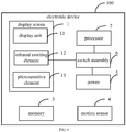
- FIG. 4 illustrates a schematic structural diagram of an electronic device according to an embodiment of the present disclosure.
- the electronic device 100 includes the display screen 1 and a processor 2.
- the display screen 1 includes a plurality of display units 11 distributed in an array throughout a display area A0 of the display screen 1.
- a plurality of infrared emitting elements 12 is embedded in a first area A1 of the display area A0 of the display screen 1.
- a plurality of photosensitive elements 13 is embedded in a second area A2 of the display area A0 of the display screen 1.
- the plurality of photosensitive elements 13 is combined into an image sensor.
- the plurality of infrared emitting elements 12 is configured to emit infrared light for illuminating a target object in front of the display screen 1, such that a plurality of light spots is formed on the target object.
- the plurality of photosensitive elements 13 is configured to receive target light spots reflected from the target object in response to the plurality of light spots and convert the target light spots into photo-electrical signals.
- the processor 2 is electrically connected to the plurality of photosensitive elements 13.
- the processor 2 is configured to perform an image processing operation to obtain a target image according to the photo-electrical signals generated by the plurality of photosensitive elements 13, and identify 3D features of the target object according to the target image.
- the processor 2 identifies 3D features of the target object according to the target image.
- the identification of the 3D features can include: comparing the target image with a reference image, determining an offset of the light spots in the target image relative to the light spots in the reference image, and/or extracting 3D features of the target object such as depth information according to the determined offset.
- the plurality of photosensitive elements 13 receives the target light spots reflected from the target object in response to the plurality of light spots and convert the target light spots into photo-electrical signals which can indicate location information of the plurality of light spots.
- the processor 2 performs an image processing operation to obtain a target image which contains the location information according to the photo-electrical signals generated by the plurality of photosensitive elements 13.
- the reference image may also contains reference location information of a plurality of reference light spots.
- the processor 2 extracts location information of the plurality of light spots form the target image and extracts reference location information of the plurality of reference light spots from the reference image.
- the processor 2 can compares the location information with the reference location information to determine an offset between the location information and the reference location information.
- FIG. 5 illustrates a schematic diagram of a target image generating process of a target object according to an embodiment of the present disclosure.
- a reference object B1 is positioned in front of the display screen 1 in a plane parallel to the display screen 1.
- the plurality of infrared emitting elements 12 emits reference infrared light to illuminate the reference object B1, such that a plurality of reference light spots is formed on the reference object B1.
- the plurality of photosensitive elements 13 receives light spots reflected from the reference object B1 in response to the plurality of reference light spots and converts the received light spots into reference photo-electrical signals.
- the processor 2 performs an image processing operation to obtain a reference image according to the reference photo-electrical signals.
- the reference image is obtained by positioning a reference object in front of the display screen 1 in a plane parallel to the display screen 1, emitting reference infrared light to illuminate the reference object by the plurality of infrared emitting elements 12 to form a plurality of reference light spots on the reference object; receiving the reference target light spots reflected from the reference object in response to the plurality of reference light spots by the plurality of photosensitive elements 13; converting the reference target light spots into reference photo-electrical signals by the plurality of photosensitive elements 13; and performing image processing operation according to the reference photo-electrical signals.
- the reference object B1 may be a two-dimensional face image.
- reference location information of the plurality of reference light spots can be determined without depth information.
- FIG. 6 illustrates a schematic diagram of a target image generating process of a target object according to an embodiment of the present disclosure.
- a target object B2 such as an user's face
- infrared light emitted by the plurality of infrared emitting elements 12 illuminate the user's face such that a plurality of light spots is formed on the user's face.
- the location of target light spots which are reflected from the user's face in response to the plurality of light spots projected on the display screen 1 may has an offset corresponding to the location of reference target light spots which are reflected from the two-dimensional face image. The size of the offset is determined by the depth information of the user's face.
- each of the photosensitive element 13 may correspond to a pixel for forming the target image.
- the location of the target light spot may be different in the target image.
- the processor 2 compares the target image with the reference image, determines the offset of the plurality of target light spots in the target image corresponding to the plurality of reference target light spots in the reference image, and extracts the 3D features such as depth information of the target object according to the offset.
- an incident angle of the infrared light emitted by the plurality of infrared emitting elements 12 may be in a reference angel range corresponding to a normal line vertical to a display plane of the display screen 1, such as in an angel range smaller than 40 degree.
- the processor 2 extracts the 3D features such as depth information of the target object according to the offset.
- the extraction of the 3D features can further include: obtaining depth information of the target object according to the determined offset of the light spots; obtaining plane information according to plane data of the target image which is obtained through an imaging processing performed by the processor 2 according to the photo-electrical signal; and further obtaining the 3D features according to the depth information and the plane information.
- the plane information can include color information (e.g., color channel data) of the target image.
- the electronic device 100 further includes a memory 3, the memory 3 is configured to store a correspondence between a reference offset and depth information.
- the processor 2 extracts the 3D features such as depth information of the target object according to the offset.
- the extraction may further include obtaining depth information of the target object corresponding to the determined offset of the light spots according to the correspondence between the offset and the depth information.
- the target object may be a user's face.
- the processor 2 may be further configured to control the plurality of infrared emitting elements 12 to emit infrared light to the front of the display screen 1 when receiving an input operation requesting face recognition verification.
- the plurality of infrared emitting elements 12 is in a standby state, and configured to emit infrared light to the front of the display screen 1 when the processor 2 received an input operation requesting face recognition verification.
- the electronic device further includes a motion sensor 4.
- the motion sensor 4 is electrically connected to the processor 2, and is configured to detect whether the electronic device 100 is moving.
- the processor 2 determines that a face recognition verification process is needed to unlock the display screen 1 when receiving an input operation requesting face recognition verification.
- the motion sensor 4 may be a sensor such as an accelerometer or a gyroscope.
- the input operation requesting face recognition verification may be configured for account login verification or payment operation verification.
- reference 3D feature information such as 3D face feature information may be stored in the memory 3.
- the processor 2 is further configured to compare 3D feature information of the target object with the reference 3D feature information when the 3D feature information of the target object is identified. After confirming that the 3D feature information of the target object matches the reference 3D feature information, the processor 2 can execute subsequent operations, such as account login verification or payment operation verification.
- the electronic device further includes a power 5 and a switch assembly 6.
- the switch assembly 6 is connected between the plurality of infrared emitting elements 12 and the power 5.
- the processor 2 controls the switch assembly 6 to enable the connection between the power 5 and the plurality of infrared emitting elements 12 when received an input operation requesting face recognition verification, then an operating voltage may be applied to the plurality of infrared emitting elements 12 to excite the plurality of infrared emitting elements 12 to emit infrared light to the front of the display screen 1.
- the switch assembly 6 may be a digital control switch, such as a MOSFET or a BJT transistor.
- the front of the display screen 1 indicates a side of the display screen 1 which is configured for displaying information.
- the memory 3 is further configured to store computer program instruction, the computer program instruction is configured to be called by the processor 2 and perform functions as mentioned in at least one of the embodiments of the present disclosure.
- the processor 2 may be a central processing unit integrated with function of image processing.
- the memory 3 may be a solid state memory, a memory card or other storage devices.
- the electronic device 100 may be handheld devices with wireless communication capabilities, in-vehicle devices, wearable devices, computing devices or other processing devices connected to wireless modems, various forms of user equipment, mobile stations, and terminal devices etc.
- the above mentioned devices are referred to as electronic devices in the present disclosure.
- a method for 3D feature recognition is further provided in the present disclosure.
- the method can be applied in the electronic device 100.
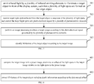
- the method may include operations at blocks illustrated in FIG. 7 .
- the block 701 emit infrared light by a plurality of infrared emitting elements 12 to illuminate a target object in front of the display screen 1, such that a plurality of light spots is formed on the target object.
- the target object may be a user's face.
- the block 701 may further include: controlling the plurality of infrared emitting elements 12 to emit infrared light to the front of the display screen 1 when receiving an input operation requesting face recognition verification, so as to illuminate a target object in front of the display screen 1, and forming a plurality of light spots on the target object.
- the receiving an input operation requesting face recognition verification may include: determining that an input operation requesting face recognition verification is received when a motion sensor 4 detects that the electronic device 100 is moving, and the display screen 1 is in a locked state.
- the receiving an input operation requesting face recognition verification may include: determining that an input operation requesting face recognition verification is received when an account login verification request or a payment operation verification request is received.
- At block 703 receiving target light spots reflected from the target object in response to the plurality of light spots, and converting the target light spots into photo-electrical signal by a plurality of photosensitive elements 13.
- the method may include: comparing 3D feature information of the target object with reference 3D feature information when the 3D feature information of the target object is identified.
- the method may further includes, after confirming that 3D feature information of the target object matches the reference 3D feature information, performing subsequent operations, such as account login verification or payment operation verification.
- FIG. 8 illustrates a sub-flow chart of operation illustrated at block 707 in FIG. 7 according to an embodiment of the present disclosure.
- the operation illustrated at block 707 may further include operations at blocks illustrated in FIG. 8 .
- comparing the target image with a reference image determining an offset of the light spots in the target image relative to the light spots in the reference image.
- the method may further include: positioning a reference object in front of the display screen 1 in a plane parallel to the display screen 1; emitting reference infrared light to illuminate the reference object by the plurality of infrared emitting elements 12, such that a plurality of reference light spots is formed on the reference object; receiving reference target light spots reflected from the reference object in response of the plurality of reference light spots, converting the reference target light spots into reference photo-electrical signals by the plurality of photosensitive elements 13; and performing image processing operation to obtain the reference image according to the reference photo-electrical signals.
- the reference image is obtained by positioning a reference object in front of the display screen 1 in a plane parallel to the display screen 1, emitting reference infrared light to illuminate the reference object by the plurality of infrared emitting elements 12 to form a plurality of reference light spots on the reference object; receiving the reference target light spots reflected from the reference object in response to the plurality of reference light spots by the plurality of photosensitive elements 13; converting the reference target light spots into reference photo-electrical signal by the plurality of photosensitive elements 13; and performing an image processing operation according to the reference photo-electrical signal.
- extracting 3D features of the target object that include depth information according to the determined offset may further includes: obtaining depth information of the target object according to the determined offset of the light spots; obtaining plane information according to plane data of the target image which is obtained through imaging processing according to the photo-electrical signals, and further obtaining the 3D feature according to the depth information and the plane information.
- extracting 3D features of the target object that include depth information according to the determined offset may further include: obtaining depth information of the target object corresponding to the determined offset of the light spots according to the correspondence between the offset and the depth information.
- a computer storage medium is further provided according to an embodiments of the present disclosure.
- the computer storage medium stores computer programs for electronic data exchange.
- the computer programs cause a computer to perform some or all of the steps of any of the methods described in the foregoing method embodiments.
- a computer program product is provided in embodiments of the present disclosure.
- the computer program product includes a non-transitory computer readable storage medium storing a computer program.
- the computer program can be operated to cause a computer to perform some or all of the steps of any of the methods described in the foregoing method embodiments.
- the processor that performs the method steps in the foregoing method embodiments may integrated with a plurality of functional units to perform each of the step, or each of the functional unit may be a physical element.
- the electronic device 100 may include multiple controllers to perform each of the step separately.
- the above integrated functional unit can be implemented in the form of hardware or in the form of a software functional module.
Landscapes
- Engineering & Computer Science (AREA)
- General Physics & Mathematics (AREA)
- Physics & Mathematics (AREA)
- Theoretical Computer Science (AREA)
- Oral & Maxillofacial Surgery (AREA)
- General Health & Medical Sciences (AREA)
- Human Computer Interaction (AREA)
- Health & Medical Sciences (AREA)
- Multimedia (AREA)
- Computer Vision & Pattern Recognition (AREA)
- Image Analysis (AREA)
- Testing, Inspecting, Measuring Of Stereoscopic Televisions And Televisions (AREA)
- Length Measuring Devices By Optical Means (AREA)
Abstract
Description
- The present disclosure relates to the field of electronic technology, and more particularly to a display screen, an electronic device and a method for three-dimensional feature recognition.
- In related art, identification components such as an infrared emitter and an infrared camera for performing three-dimensional (3D) feature (such as 3D face feature) recognition generally need to be disposed outside an display area of an electronic device, so that a non-display area needs to be reserved to dispose these components, which limited a further increasing of the display area.
- The technical problem to be solved in the present disclosure is to provide a display screen, an electronic device and a method for 3D feature recognition, which can increase a screen-to-body ratio.
- In an aspect of the present disclosure, a display screen is provided. The display screen includes a plurality of display units distributed in an array across a display area of the display screen, a plurality of infrared emitting elements embedded in a first area of the display area, and a plurality of photosensitive elements embedded in a second area of the display area of the display screen. The plurality of infrared emitting elements is configured to emit infrared light for illuminating a target object in front of the display screen so as to form a plurality of light spots on the target object. The plurality of photosensitive elements is configured to receive target light spots reflected from the target object and convert the target light spots into photo-electrical signals suitable for generating a target image of the target object.
- In another aspect of the present disclosure, an electronic device is further provided. The electronic device includes a display screen and a processor. The display screen includes a plurality of display units distributed in an array across a display area of the display screen, a plurality of infrared emitting elements embedded in a first area of the display area, and a plurality of photosensitive elements embedded in a second area of the display area. The plurality of infrared emitting elements is configured to emit infrared light for illuminating a target object in front of the display screen so as to form a plurality of light spots on the target object. The plurality of photosensitive elements is configured to receive target light spots reflected from the target object and convert the target light spots into photo-electrical signals. The processor is electrically connected to the plurality of photosensitive elements, and configured to perform an image processing operation to obtain a target image according to the photo-electrical signals generated by the plurality of photosensitive elements, and to identify one or more 3D features of the target object according to the target image.
- In an additional aspect of the present disclosure, a 3D feature recognition method is provided. The method includes emitting infrared light by a plurality of infrared emitting elements of a display screen to illuminate a target object in front of the display screen so as to form a plurality of light spots on the target object, receiving, by a plurality of photosensitive elements of the display screen, target light spots reflected from the target object, converting the target light spots into photo-electrical signals by the plurality of photosensitive elements, performing an image processing operation to obtain a target image according to the photo-electrical signals generated by the plurality of photosensitive elements, and identifying one or more 3D features of the target object according to the target image.
- In the display screen, the electronic device and the method for 3D feature recognition of the present disclosure, a 3D feature recognition assembly, such as the plurality of infrared emitting elements and the plurality of photosensitive elements, is embedded in the display area of the display. As a result, there is no need to reserve extra non-display area to place the 3D feature recognition assembly, which can increase screen to body ratio of the display screen effectively and meet the needs of 3D feature recognition such as 3D face feature recognition.
- In order to describe more clearly technical solutions of the present disclosure, the following will give a brief introduction to the accompanying drawings related to embodiments of the present disclosure. Apparently, the following accompanying drawings merely illustrate some embodiments of the present disclosure. Those of ordinary skill in the art can also obtain other accompanying drawings based on the following accompanying drawings without making creative effort.
-
FIG. 1 is a schematic structural diagram illustrating a display screen according to an embodiment of the present disclosure; -
FIG. 2 is a schematic structural diagram illustrating a display screen according to another embodiment of the present disclosure; -
FIG. 3 is a schematic structural diagram illustrating a display screen according to an additional embodiment of the present disclosure; -
FIG. 4 is a schematic structural diagram illustrating an electronic device according to an embodiment of the present disclosure; -
FIG. 5 is a schematic diagram of a generating process of a reference image according to an embodiment of the present disclosure; -
FIG. 6 is a schematic diagram of a target image generating process of a target object according to an embodiment of the present disclosure; -
FIG. 7 is a flow chart of a 3D feature recognition method according to an embodiment of the present disclosure; and -
FIG. 8 is a sub-flow chart of operation illustrated atblock 707 inFIG. 7 according to an embodiment of the present disclosure. - In the following, embodiments of the present disclosure will be elaborated with reference to the accompanying drawings.
-
FIG. 1 is a schematic structural diagram illustrating adisplay screen 1 according to an embodiment of the present disclosure. - As illustrated in
FIG. 1 , thedisplay screen 1 includes a display area A0. A plurality ofdisplay units 11 is distributed in an array throughout the display area A0 of thedisplay screen 1. A plurality ofinfrared emitting elements 12 is embedded in a first area A1 of the display area A0 of thedisplay screen 1, and a plurality ofphotosensitive elements 13 is embedded in a second area A2 of the display area A0 of thedisplay screen 1. The plurality ofphotosensitive elements 13 is combined into an image sensor. - The plurality of
infrared emitting elements 12 is configured to emit infrared light for illuminating a target object in front of thedisplay screen 1, such that a plurality of light spots is formed on the target object. The plurality ofphotosensitive elements 13 is configured to receive target light spots reflected from the target object in response to the plurality of light spots and convert the target light spots into photo-electrical signals suitable for generating a target image for identifying 3D feature of the target object. The target light spots may include a plurality of reflecting light spots reflected by the target object in response to the plurality of light spots. - In the present disclosure, a 3D feature recognition assembly, such as the plurality of
infrared emitting elements 12 and the plurality ofphotosensitive elements 13, is embedded in the display area A0 of thedisplay 1. As a result, there is no need to reserve extra non-display area to place the 3D feature recognition assembly, which can increase screen to body ratio of the display screen effectively and meet the needs of 3D feature recognition such as 3D face feature recognition. - In one embodiment, the first area A1 and the second area A2 overlap to form an overlapped area. In some embodiments, the first area A1 and the second area A2 completely overlap with each other (e.g., as shown in
FIG. 1-2 ). In some embodiments, the size of the overlapped area may be greater than or equal to half of the size of the display area A0. - In one embodiment, the plurality of
infrared emitting elements 12 and the plurality ofphotosensitive elements 13 are embedded in the same area of the display area A0 of thedisplay 1, and distributed in at least half of the display area A0. - In one embodiment, as illustrated in
FIG. 1 , the first area A1 and the second area A2 overlap with the display area A0, which means the plurality ofinfrared emitting elements 12 and the plurality ofphotosensitive elements 13 are embedded in entire of the display area A0. - As illustrated in
FIG. 2 , in one embodiment, the size of the overlapped area may be smaller than the size of the display area A0 and greater than or equal to half of the size of the display area A0. The overlapped area may be located in any position of the display area A0, and the size of the overlapped area may be greater than or equal to half of the size of the display area A0. - By way of example, as illustrated in
FIG. 2 , the overlapped area may be located in a center area of the display area A0. As an example, the overlapped area may be located in an area close to the end of the display area A0. The size of the overlapped area may be greater than or equal to half of the size of the display area A0. - As illustrated in
FIG.1 andFIG. 2 , in the overlapped area, each of thedisplay units 11 includes aninfrared emitting element 12 and aphotosensitive element 13, which means in the overlapped area, the number of theinfrared emitting element 12 and the number of thephotosensitive element 13 are equal to the number of thedisplay units 11. - In one embodiment, the number of the
infrared emitting element 12 and the number of thephotosensitive element 13 may be equal to each other, and greater or smaller than the number of thedisplay unit 11. By way of example, aninfrared emitting element 12 and aphotosensitive element 13 may correspond to every two of thedisplay units 11. As another example, twoinfrared emitting elements 12 and twophotosensitive elements 13 correspond to each of thedisplay units 11. - In another embodiment, in the overlapped area, the number of the
infrared emitting element 12 and the number of thephotosensitive element 13 may be different. By way of example, the number of theinfrared emitting element 12 may be greater or smaller than the number of thephotosensitive element 13. - As illustrated in
FIG. 3 , the first area A1 occupies half of the display area A0, and the second area A2 occupies the other half area of the display area A0. - In some embodiments, the first area A1 and the second area A2 are two symmetrical areas with respect to a center line L1 of the display area A0. The center line L1 is parallel to one side of the display area A0. By way of example, as shown in
FIG. 3 , the first area A1 is in an upper half area of the display area A0, and the second area A2 is in a lower half area of the display area A0. The first area A1 and the second area A2 are symmetrical with respect to the center line L1. In at least one alternative embodiment, the first area A1 may be in a left half area of the display area A0, and the second area A2 may be in a right half area of the display area A0. - In some embodiments, the first area A1 and the second area A2 may be two symmetrical areas with respect to a diagonal of the display area A0. By way of example, the display area A0 may be divided into two areas by a diagonal defined between an upper left corner and a lower right corner. The first area A1 may be in a lower left area of the display area A0, and the second area A2 may be in an upper right area of the display area A0.
- In some embodiments, each of the
display unit 11 includes an infrared emittingelement 12 in the first area A1, and each of thedisplay units 11 includes aphotosensitive element 13 in the second area A2. In the first area A1, the number of the infrared emittingelement 12 may be equal to the number of thedisplay unit 11. In the second area A2, the number of thephotosensitive element 13 may be equal to the number of thedisplay unit 11. In other embodiments, the number of the infrared emittingelement 12 may be different than the number of thedisplay unit 11 in the first area A1. The number of thephotosensitive element 13 may be different to the number of thedisplay unit 11 in the second area A2. - In some embodiments, each of the
display unit 11 corresponds to a pixel of thedisplay screen 1. The number of thedisplay unit 11 is determined by the resolution of thedisplay screen 1. - In some embodiments, the plurality of infrared emitting
elements 12 embedded in the first area A1 is configured to emit infrared light for illuminating the target object in front of thedisplay screen 1. The infrared light reflected by the target object can form the target light spots. The plurality ofphotosensitive elements 13 is configured to receive the target light spots and convert the target light spots into photo-electrical signals suitable for generating a target image for identifying 3D feature of the target object. - In the present disclosure, the display screen may be an Organic Light Emitting Diode (OLED) display. Each of the
display unit 11 includes one or more organic light emitting diode. - In some embodiments, the display screen may be a Liquid crystal display (LCD). Each of the
display unit 11 includes three liquid crystal units, a red color filter, a green color filter and a blue color filter, each of the red color filter, the green color filter and the blue color filter being positioned above one of the liquid crystal unit so as to form adisplay unit 11 including a red sub-pixel, a green sub-pixel and a blue sub-pixel. - As illustrated in
FIG. 1 , in some embodiments, thedisplay screen 1 may include a non-display area F0 surrounding the display area A0. Since the 3D feature recognition assembly, such as the plurality of infrared emittingelements 12 and the plurality ofphotosensitive elements 13, is embedded in the display area A0 of thedisplay 1, the non-display area can be reduced to much smaller than a traditional display screen. In other embodiments, the non-display area can be eliminated, the display screen may include a display area only, so as to realize a real full screen. -
FIG. 4 illustrates a schematic structural diagram of an electronic device according to an embodiment of the present disclosure. Theelectronic device 100 includes thedisplay screen 1 and aprocessor 2. - As illustrated in some embodiments, the
display screen 1 includes a plurality ofdisplay units 11 distributed in an array throughout a display area A0 of thedisplay screen 1. A plurality of infrared emittingelements 12 is embedded in a first area A1 of the display area A0 of thedisplay screen 1. A plurality ofphotosensitive elements 13 is embedded in a second area A2 of the display area A0 of thedisplay screen 1. The plurality ofphotosensitive elements 13 is combined into an image sensor. The plurality of infrared emittingelements 12 is configured to emit infrared light for illuminating a target object in front of thedisplay screen 1, such that a plurality of light spots is formed on the target object. The plurality ofphotosensitive elements 13 is configured to receive target light spots reflected from the target object in response to the plurality of light spots and convert the target light spots into photo-electrical signals. - The
processor 2 is electrically connected to the plurality ofphotosensitive elements 13. Theprocessor 2 is configured to perform an image processing operation to obtain a target image according to the photo-electrical signals generated by the plurality ofphotosensitive elements 13, and identify 3D features of the target object according to the target image. - In some embodiments, the
processor 2 identifies 3D features of the target object according to the target image. The identification of the 3D features can include: comparing the target image with a reference image, determining an offset of the light spots in the target image relative to the light spots in the reference image, and/or extracting 3D features of the target object such as depth information according to the determined offset. - In some embodiments, the plurality of
photosensitive elements 13 receives the target light spots reflected from the target object in response to the plurality of light spots and convert the target light spots into photo-electrical signals which can indicate location information of the plurality of light spots. Theprocessor 2 performs an image processing operation to obtain a target image which contains the location information according to the photo-electrical signals generated by the plurality ofphotosensitive elements 13. The reference image may also contains reference location information of a plurality of reference light spots. - The
processor 2 extracts location information of the plurality of light spots form the target image and extracts reference location information of the plurality of reference light spots from the reference image. Theprocessor 2 can compares the location information with the reference location information to determine an offset between the location information and the reference location information. -
FIG. 5 illustrates a schematic diagram of a target image generating process of a target object according to an embodiment of the present disclosure. A reference object B1 is positioned in front of thedisplay screen 1 in a plane parallel to thedisplay screen 1. The plurality of infrared emittingelements 12 emits reference infrared light to illuminate the reference object B1, such that a plurality of reference light spots is formed on the reference object B1. The plurality ofphotosensitive elements 13 receives light spots reflected from the reference object B1 in response to the plurality of reference light spots and converts the received light spots into reference photo-electrical signals. Theprocessor 2 performs an image processing operation to obtain a reference image according to the reference photo-electrical signals. - In the present disclosure, the reference image is obtained by positioning a reference object in front of the
display screen 1 in a plane parallel to thedisplay screen 1, emitting reference infrared light to illuminate the reference object by the plurality of infrared emittingelements 12 to form a plurality of reference light spots on the reference object; receiving the reference target light spots reflected from the reference object in response to the plurality of reference light spots by the plurality ofphotosensitive elements 13; converting the reference target light spots into reference photo-electrical signals by the plurality ofphotosensitive elements 13; and performing image processing operation according to the reference photo-electrical signals. - In some embodiments, the reference object B1 may be a two-dimensional face image. By performing an imaging processing operation according to the photo-electrical signals obtained from the reference object B1, reference location information of the plurality of reference light spots can be determined without depth information.
-
FIG. 6 illustrates a schematic diagram of a target image generating process of a target object according to an embodiment of the present disclosure. When a target object B2 such as an user's face is positioned in front of thedisplay screen 1, due to the unevenness of the user's face, infrared light emitted by the plurality of infrared emittingelements 12 illuminate the user's face such that a plurality of light spots is formed on the user's face. The location of target light spots which are reflected from the user's face in response to the plurality of light spots projected on thedisplay screen 1 may has an offset corresponding to the location of reference target light spots which are reflected from the two-dimensional face image. The size of the offset is determined by the depth information of the user's face. - In some embodiments, when different targets such as different user's face are positioned in front of the
display screen 1, due to differences in facial contours, light spots formed on the user's face may be reflected and from different target light spots projected on differentphotosensitive elements 13, and received by differentphotosensitive elements 13. Each of thephotosensitive element 13 may correspond to a pixel for forming the target image. As a result, when differentphotosensitive element 13 receive different target light spots, the location of the target light spot may be different in the target image. - As a result, the
processor 2 compares the target image with the reference image, determines the offset of the plurality of target light spots in the target image corresponding to the plurality of reference target light spots in the reference image, and extracts the 3D features such as depth information of the target object according to the offset. - In some embodiments, an incident angle of the infrared light emitted by the plurality of infrared emitting
elements 12 may be in a reference angel range corresponding to a normal line vertical to a display plane of thedisplay screen 1, such as in an angel range smaller than 40 degree. - In some embodiments, the
processor 2 extracts the 3D features such as depth information of the target object according to the offset. The extraction of the 3D features can further include: obtaining depth information of the target object according to the determined offset of the light spots; obtaining plane information according to plane data of the target image which is obtained through an imaging processing performed by theprocessor 2 according to the photo-electrical signal; and further obtaining the 3D features according to the depth information and the plane information. In some embodiments, the plane information can include color information (e.g., color channel data) of the target image. - As illustrated in
FIG. 4 , in some embodiments, theelectronic device 100 further includes amemory 3, thememory 3 is configured to store a correspondence between a reference offset and depth information. - The
processor 2 extracts the 3D features such as depth information of the target object according to the offset. The extraction may further include obtaining depth information of the target object corresponding to the determined offset of the light spots according to the correspondence between the offset and the depth information. - In one embodiment, the target object may be a user's face. The
processor 2 may be further configured to control the plurality of infrared emittingelements 12 to emit infrared light to the front of thedisplay screen 1 when receiving an input operation requesting face recognition verification. In some embodiments, the plurality of infrared emittingelements 12 is in a standby state, and configured to emit infrared light to the front of thedisplay screen 1 when theprocessor 2 received an input operation requesting face recognition verification. - As illustrated in
FIG. 4 , the electronic device further includes amotion sensor 4. Themotion sensor 4 is electrically connected to theprocessor 2, and is configured to detect whether theelectronic device 100 is moving. When themotion sensor 4 detects that theelectronic device 100 is moving, and thedisplay screen 1 is in a locked state, theprocessor 2 determines that a face recognition verification process is needed to unlock thedisplay screen 1 when receiving an input operation requesting face recognition verification. Here, themotion sensor 4 may be a sensor such as an accelerometer or a gyroscope. - In other embodiments, the input operation requesting face recognition verification may be configured for account login verification or payment operation verification.
- In some embodiments,
reference 3D feature information such as 3D face feature information may be stored in thememory 3. Theprocessor 2 is further configured to compare 3D feature information of the target object with thereference 3D feature information when the 3D feature information of the target object is identified. After confirming that the 3D feature information of the target object matches thereference 3D feature information, theprocessor 2 can execute subsequent operations, such as account login verification or payment operation verification. - As illustrated in
FIG. 4 , the electronic device further includes apower 5 and aswitch assembly 6. Theswitch assembly 6 is connected between the plurality of infrared emittingelements 12 and thepower 5. Theprocessor 2 controls theswitch assembly 6 to enable the connection between thepower 5 and the plurality of infrared emittingelements 12 when received an input operation requesting face recognition verification, then an operating voltage may be applied to the plurality of infrared emittingelements 12 to excite the plurality of infrared emittingelements 12 to emit infrared light to the front of thedisplay screen 1. - In one embodiment, the
switch assembly 6 may be a digital control switch, such as a MOSFET or a BJT transistor. - In one embodiment, the front of the
display screen 1 indicates a side of thedisplay screen 1 which is configured for displaying information. - In one embodiment, the
memory 3 is further configured to store computer program instruction, the computer program instruction is configured to be called by theprocessor 2 and perform functions as mentioned in at least one of the embodiments of the present disclosure. - In one embodiment, the
processor 2 may be a central processing unit integrated with function of image processing. Thememory 3 may be a solid state memory, a memory card or other storage devices. - In the present disclosure, the
electronic device 100 may be handheld devices with wireless communication capabilities, in-vehicle devices, wearable devices, computing devices or other processing devices connected to wireless modems, various forms of user equipment, mobile stations, and terminal devices etc. For convenience of description, the above mentioned devices are referred to as electronic devices in the present disclosure. - As illustrated in
FIG. 7 , a method for 3D feature recognition is further provided in the present disclosure. The method can be applied in theelectronic device 100. The method may include operations at blocks illustrated inFIG. 7 . - At
block 701, emit infrared light by a plurality of infrared emittingelements 12 to illuminate a target object in front of thedisplay screen 1, such that a plurality of light spots is formed on the target object. In some embodiments, the target object may be a user's face. Theblock 701 may further include: controlling the plurality of infrared emittingelements 12 to emit infrared light to the front of thedisplay screen 1 when receiving an input operation requesting face recognition verification, so as to illuminate a target object in front of thedisplay screen 1, and forming a plurality of light spots on the target object. - In some embodiments, the receiving an input operation requesting face recognition verification may include: determining that an input operation requesting face recognition verification is received when a
motion sensor 4 detects that theelectronic device 100 is moving, and thedisplay screen 1 is in a locked state. - In other embodiments, the receiving an input operation requesting face recognition verification may include: determining that an input operation requesting face recognition verification is received when an account login verification request or a payment operation verification request is received.
- At
block 703, receiving target light spots reflected from the target object in response to the plurality of light spots, and converting the target light spots into photo-electrical signal by a plurality ofphotosensitive elements 13. - At
block 705, performing an image processing operation to obtain a target image according to the photo-electrical signal generated by the plurality ofphotosensitive elements 13. - At
block 707, identifying 3D feature of the target object according to the target image. - In some embodiments, the method may include: comparing 3D feature information of the target object with
reference 3D feature information when the 3D feature information of the target object is identified. The method may further includes, after confirming that 3D feature information of the target object matches thereference 3D feature information, performing subsequent operations, such as account login verification or payment operation verification. -
FIG. 8 illustrates a sub-flow chart of operation illustrated atblock 707 inFIG. 7 according to an embodiment of the present disclosure. The operation illustrated atblock 707 may further include operations at blocks illustrated inFIG. 8 . - At
block 801, comparing the target image with a reference image, determining an offset of the light spots in the target image relative to the light spots in the reference image. - At
block 803, extracting 3D feature of the target object such as depth information according to the determined offset. - In some embodiments, the method may further include: positioning a reference object in front of the
display screen 1 in a plane parallel to thedisplay screen 1; emitting reference infrared light to illuminate the reference object by the plurality of infrared emittingelements 12, such that a plurality of reference light spots is formed on the reference object; receiving reference target light spots reflected from the reference object in response of the plurality of reference light spots, converting the reference target light spots into reference photo-electrical signals by the plurality ofphotosensitive elements 13; and performing image processing operation to obtain the reference image according to the reference photo-electrical signals. - In the present disclosure, the reference image is obtained by positioning a reference object in front of the
display screen 1 in a plane parallel to thedisplay screen 1, emitting reference infrared light to illuminate the reference object by the plurality of infrared emittingelements 12 to form a plurality of reference light spots on the reference object; receiving the reference target light spots reflected from the reference object in response to the plurality of reference light spots by the plurality ofphotosensitive elements 13; converting the reference target light spots into reference photo-electrical signal by the plurality ofphotosensitive elements 13; and performing an image processing operation according to the reference photo-electrical signal. - In some embodiments, extracting 3D features of the target object that include depth information according to the determined offset may further includes: obtaining depth information of the target object according to the determined offset of the light spots; obtaining plane information according to plane data of the target image which is obtained through imaging processing according to the photo-electrical signals, and further obtaining the 3D feature according to the depth information and the plane information.
- In some embodiments, extracting 3D features of the target object that include depth information according to the determined offset may further include: obtaining depth information of the target object corresponding to the determined offset of the light spots according to the correspondence between the offset and the depth information.
- A computer storage medium is further provided according to an embodiments of the present disclosure. The computer storage medium stores computer programs for electronic data exchange. The computer programs cause a computer to perform some or all of the steps of any of the methods described in the foregoing method embodiments.
- A computer program product is provided in embodiments of the present disclosure. The computer program product includes a non-transitory computer readable storage medium storing a computer program. The computer program can be operated to cause a computer to perform some or all of the steps of any of the methods described in the foregoing method embodiments.
- It should be noted that, for the foregoing method embodiments, for the sake of brevity, they are all described as a series of action combinations, but those skilled in the art should understand that the present disclosure is not limited by the described action sequence. Because certain steps may be performed in other sequences or concurrently in accordance with the present disclosure. In the following, those skilled in the art should also understand that the embodiments described in the specification are all preferred embodiments, and the actions and circuits involved are not necessarily required by the present disclosure.
- In the above embodiments, the descriptions of the various embodiments are all focused on, and the parts that are not detailed in a certain embodiment can be referred to the related descriptions of other embodiments.
- In addition, the processor that performs the method steps in the foregoing method embodiments may integrated with a plurality of functional units to perform each of the step, or each of the functional unit may be a physical element. For example, the
electronic device 100 may include multiple controllers to perform each of the step separately. The above integrated functional unit can be implemented in the form of hardware or in the form of a software functional module.
Claims (15)
- A display screen (1), comprising:a plurality of display units (11) distributed in an array across a display area (A0) of the display screen (1);a plurality of infrared emitting elements (12) embedded in a first area (A1) of the display area (A0), the plurality of infrared emitting elements (12) configured to emit infrared light for illuminating a target object in front of the display screen (1) so as to form a plurality of light spots on the target object; anda plurality of photosensitive elements (13) embedded in a second area (A2) of the display area (A0), the plurality of photosensitive elements (13) configured to receive target light spots reflected from the target object and convert the target light spots into photo-electrical signals suitable for generating a target image of the target object.
- The display screen of claim 1, wherein the first area (A1) and the second area (A2) overlap, and wherein a size of at least one of the first area (A1) or the second area (A2) is greater than or equal to half of the display area (A0), and wherein in an overlapped area formed by the first area (A1) and the second area (A2), each of the display units (11) comprises an infrared emitting element (12) and a photosensitive element (13).
- The display screen of claim 1, wherein the first area (A1) is in a first half of the display area (A0), and wherein the second area (A2) is in a second half of the display area (A0), and wherein each of the plurality of display units (11) comprises an infrared emitting element (12) in the first area (A1), and a photosensitive element (13) in the second area (A2).
- An electronic device (100), comprising:a display screen (1) that includes:a plurality of display units (11) distributed in an array across a display area (A0) of the display screen (1),a plurality of infrared emitting elements (12) embedded in a first area (A1) of the display area (A0), anda plurality of photosensitive elements (13) embedded in a second area (A2) of the display area (A0),wherein the plurality of infrared emitting elements (12) is configured to emit infrared light for illuminating a target object in front of the display screen (1) so as to form a plurality of light spots on the target object, andwherein the plurality of photosensitive elements (13) is configured to receive target light spots reflected from the target object and convert the target light spots into photo-electrical signals; anda processor (2) electrically connected to the plurality of photosensitive elements (13), the processor (2) configured to perform an image processing operation to obtain a target image according to the photo-electrical signals generated by the plurality of photosensitive elements (13), and to identify one or more 3D features of the target object according to the target image.
- The electronic device of claim 4, wherein the processor (2) is configured to identify the one or more 3D features of the target object according to the target image by:comparing the target image with a reference image,determining an offset of the target light spots in the target image relative to light spots in the reference image;extracting the one or more 3D features of the target object according to the determined offset, wherein the one or more 3D features include depth information of the target object.
- The electronic device of claim 5, wherein the reference image is obtained by:emitting reference infrared light to illuminate a reference object by the plurality of infrared emitting elements (A1) to form a plurality of reference light spots on the reference object, wherein the reference object is located in front of the display screen (1) and in parallel to the display screen (1);receiving light spots reflected from the reference object;converting the received light spots into reference photo-electrical signals by the plurality of photosensitive elements (13); andperforming an image processing operation according to the reference photo-electrical signals.
- The electronic device of claim 5, wherein the processor (2) is further configured to:determining depth information of the target object according to the determined offset of the light spots;determining plane information according to plane data of the target image, wherein the plane data of the target image is obtained through the imaging processing operation performed by the processor (2) according to the photo-electrical signals; anddetermining the one or more 3D features according to the depth information and the plane information.
- The electronic device of claim 4, wherein the first area (A1) and the second area (A2) overlap, and wherein a size of at least one of the first area (A1) or the second area (A2) is greater than or equal to half of the display area (A0), and wherein, in an overlapped area of the first area (A1) and second area (A2), each of the plurality of display units (11) comprises an infrared emitting element (12) and a photosensitive element (13).
- The electronic device of claim 4, wherein the first area (A1) is in a first half area of the display area (A0), and wherein the second area (A2) is in a second half area of the display area (A0), and wherein each of the plurality of display units (11) comprises an infrared emitting element (12) in the first area (A1), and a photosensitive element (13) in the second area (A2).
- The electronic device of claim 4, wherein the target object includes a face of a user, and wherein the processor (2) is further configured to:
control the plurality of infrared emitting elements (12) to emit infrared light to the front of the display screen (1) upon receiving an input operation requesting face recognition verification. - The electronic device of claim 10, wherein the electronic device (100) further comprises a power (5) and a switch assembly (6), the switch assembly (6) connected between the plurality of infrared emitting elements (12) and the power (5), and wherein the processor (2) is further configured to:
control the switch assembly (6) to enable a connection between the power (5) and the plurality of infrared emitting elements (12) upon receiving an input operation requesting face recognition verification so as to apply an operating voltage to the plurality of infrared emitting elements (12) to excite the plurality of infrared emitting elements (12) to emit infrared light to a front of the display screen (1). - A method for 3D feature recognition, comprising:emitting infrared light by a plurality of infrared emitting elements (12) of a display screen (1) to illuminate a target object in front of the display screen (1) so as to form a plurality of light spots on the target object;receiving, by a plurality of photosensitive elements (13) of the display screen (1), target light spots reflected from the target object;converting the target light spots into photo-electrical signals by the plurality of photosensitive elements (13);performing an image processing operation to obtain a target image according to the photo-electrical signals generated by the plurality of photosensitive elements (13); andidentifying one or more 3D features of the target object according to the target image.
- The method of claim 12, wherein identifying the one or more 3D features of the target comprises:comparing the target image with a reference image;determining an offset of the target light spots in the target image relative to light spots in the reference image; andextracting the one or more 3D features of the target object according to the determined offset, wherein the one or more 3D features include depth information of the target object.
- The method of claim 13, further comprising:emitting reference infrared light to illuminate a reference object by the plurality of infrared emitting elements (12) so as to form a plurality of reference light spots on the reference object, wherein the reference object is positioned in front of the display screen (1) and in parallel to the display screen (1);receiving light spots reflected from the reference object;converting the received light spots into reference photo-electrical signals by the plurality of photosensitive elements (13); andperforming an image processing operation to obtain the reference image according to the reference photo-electrical signals.
- The method of claim 13, wherein extracting the one or more 3D features of the target object comprises:determining depth information of the target object according to the determined offset of the light spots;determining plane information according to plane data of the target image, wherein the planar data of the target image is obtained through the imaging processing operation according to the photo-electrical signal, anddetermining the one or more 3D features according to the depth information and the plane information.
Applications Claiming Priority (2)
| Application Number | Priority Date | Filing Date | Title |
|---|---|---|---|
| CN201810914142.7A CN109040363B (en) | 2018-08-10 | 2018-08-10 | Display screen, electronic device and three-dimensional feature recognition method |
| CN201821295039.0U CN208489880U (en) | 2018-08-10 | 2018-08-10 | Display screen and electronic device |
Publications (1)
| Publication Number | Publication Date |
|---|---|
| EP3608837A1 true EP3608837A1 (en) | 2020-02-12 |
Family
ID=67587446
Family Applications (1)
| Application Number | Title | Priority Date | Filing Date |
|---|---|---|---|
| EP19190662.7A Withdrawn EP3608837A1 (en) | 2018-08-10 | 2019-08-08 | Display screen, electronic device and method for three-dimensional feature recognition |
Country Status (3)
| Country | Link |
|---|---|
| US (1) | US11081516B2 (en) |
| EP (1) | EP3608837A1 (en) |
| WO (1) | WO2020030151A1 (en) |
Families Citing this family (3)
| Publication number | Priority date | Publication date | Assignee | Title |
|---|---|---|---|---|
| EP3913912B1 (en) | 2019-01-14 | 2025-05-07 | BOE Technology Group Co., Ltd. | Display apparatus, electronic device, and driving method for display apparatus |
| US11478533B2 (en) | 2020-04-27 | 2022-10-25 | Novo Nordisk A/S | Semaglutide for use in medicine |
| WO2022261980A1 (en) | 2021-06-18 | 2022-12-22 | 苏州晶湛半导体有限公司 | Display panel |
Citations (2)
| Publication number | Priority date | Publication date | Assignee | Title |
|---|---|---|---|---|
| US20150364107A1 (en) * | 2014-06-17 | 2015-12-17 | LuxVue Technology Corporation | Interactive display panel with ir diodes |
| US20180198980A1 (en) * | 2017-01-06 | 2018-07-12 | Intel Corporation | Integrated Image Sensor and Display Pixel |
Family Cites Families (18)
| Publication number | Priority date | Publication date | Assignee | Title |
|---|---|---|---|---|
| JP4645822B2 (en) * | 2005-04-19 | 2011-03-09 | ソニー株式会社 | Image display device and object detection method |
| US7532181B2 (en) * | 2005-07-20 | 2009-05-12 | Eastman Kodak Company | Visible and invisible image display |
| KR101526012B1 (en) | 2008-10-30 | 2015-06-05 | 삼성전자주식회사 | Method and apparatus for data communication using digital image processing |
| US20150253428A1 (en) * | 2013-03-15 | 2015-09-10 | Leap Motion, Inc. | Determining positional information for an object in space |
| US20140085245A1 (en) * | 2012-09-21 | 2014-03-27 | Amazon Technologies, Inc. | Display integrated camera array |
| AU2014280332B2 (en) * | 2013-06-13 | 2017-09-07 | Basf Se | Detector for optically detecting at least one object |
| KR102201732B1 (en) * | 2013-09-26 | 2021-01-12 | 엘지전자 주식회사 | Digital device and method for controlling the same |
| US20160309135A1 (en) * | 2015-04-20 | 2016-10-20 | Ilia Ovsiannikov | Concurrent rgbz sensor and system |
| CN106980460B (en) | 2017-03-31 | 2020-06-02 | 盐城政豪网络科技有限公司 | Mobile terminal and image processing method |
| CN207233359U (en) | 2017-08-17 | 2018-04-13 | 深圳信炜科技有限公司 | Display module and electronic equipment |
| CN107946338B (en) | 2017-08-17 | 2020-07-28 | 深圳信炜科技有限公司 | Display modules and electronic equipment |
| KR102681300B1 (en) * | 2017-08-28 | 2024-07-04 | 트리나미엑스 게엠베하 | A detector that determines the position of at least one object |
| CN107742631B (en) * | 2017-10-26 | 2020-02-14 | 京东方科技集团股份有限公司 | Depth imaging device, display panel, method of manufacturing depth imaging device, and apparatus |
| CN111587384B (en) * | 2017-11-17 | 2024-06-14 | 特里纳米克斯股份有限公司 | A detector for determining a position of at least one object |
| CN107844247B (en) | 2017-11-22 | 2021-04-02 | Oppo广东移动通信有限公司 | Display components and electronic equipment |
| US11200408B2 (en) * | 2017-11-28 | 2021-12-14 | Fingerprint Cards Anacatum Ip Ab | Biometric imaging system and method for controlling the system |
| KR102470004B1 (en) * | 2018-01-23 | 2022-11-24 | 삼성전자주식회사 | Infrared element mounted display and electronic device including thereof |
| CN109040363B (en) | 2018-08-10 | 2024-03-19 | Oppo广东移动通信有限公司 | Display screen, electronic device and three-dimensional feature recognition method |
-
2019
- 2019-08-06 US US16/533,188 patent/US11081516B2/en active Active
- 2019-08-08 EP EP19190662.7A patent/EP3608837A1/en not_active Withdrawn
- 2019-08-09 WO PCT/CN2019/100089 patent/WO2020030151A1/en not_active Ceased
Patent Citations (2)
| Publication number | Priority date | Publication date | Assignee | Title |
|---|---|---|---|---|
| US20150364107A1 (en) * | 2014-06-17 | 2015-12-17 | LuxVue Technology Corporation | Interactive display panel with ir diodes |
| US20180198980A1 (en) * | 2017-01-06 | 2018-07-12 | Intel Corporation | Integrated Image Sensor and Display Pixel |
Also Published As
| Publication number | Publication date |
|---|---|
| WO2020030151A1 (en) | 2020-02-13 |
| US11081516B2 (en) | 2021-08-03 |
| US20200052030A1 (en) | 2020-02-13 |
Similar Documents
| Publication | Publication Date | Title |
|---|---|---|
| US11025814B2 (en) | Electronic device for storing depth information in connection with image depending on properties of depth information obtained using image and control method thereof | |
| US9992474B2 (en) | Stereo depth camera using VCSEL with spatially and temporally interleaved patterns | |
| US20200021729A1 (en) | Control method, control device and computer device | |
| KR102472156B1 (en) | Electronic Device and the Method for Generating Depth Information thereof | |
| KR102655532B1 (en) | Electronic device and method for acquiring biometric information using light of display | |
| EP3608837A1 (en) | Display screen, electronic device and method for three-dimensional feature recognition | |
| CN109040363B (en) | Display screen, electronic device and three-dimensional feature recognition method | |
| KR102679543B1 (en) | Electronic device for changing display of designated area of display and operating method thereof | |
| CN108399596A (en) | Depth image engine and depth image computational methods | |
| CN109587303B (en) | Electronic Devices and Mobile Platforms | |
| US20230269492A1 (en) | Electronic device and method for displaying image in electronic device | |
| US10819897B2 (en) | Electronic device and method for controlling autofocus of camera | |
| CN113052884A (en) | Information processing method, information processing apparatus, storage medium, and electronic device | |
| WO2019214641A1 (en) | Optical tag based information apparatus interaction method and system | |
| KR20200101233A (en) | Electronic device and method for providing service corresponding to selection of object in image | |
| US10089510B2 (en) | Display control methods and apparatuses | |
| US10733920B2 (en) | Image processing apparatus, method for controlling the same, and storage medium | |
| CN109803089B (en) | Electronic Devices and Mobile Platforms | |
| CN105677030B (en) | A kind of control method and electronic equipment | |
| US11228744B2 (en) | Method for controlling projection system, projection system, and control program | |
| CN112752088B (en) | Depth image generation method and device, reference image generation method and electronic equipment | |
| CN111062969B (en) | Target tracking method and related product | |
| WO2019004594A1 (en) | Curved display device and operating method therefor | |
| CN208489880U (en) | Display screen and electronic device | |
| CN111881836B (en) | Target object identification method and related device and equipment |
Legal Events
| Date | Code | Title | Description |
|---|---|---|---|
| PUAI | Public reference made under article 153(3) epc to a published international application that has entered the european phase |
Free format text: ORIGINAL CODE: 0009012 |
|
| STAA | Information on the status of an ep patent application or granted ep patent |
Free format text: STATUS: THE APPLICATION HAS BEEN PUBLISHED |
|
| AK | Designated contracting states |
Kind code of ref document: A1 Designated state(s): AL AT BE BG CH CY CZ DE DK EE ES FI FR GB GR HR HU IE IS IT LI LT LU LV MC MK MT NL NO PL PT RO RS SE SI SK SM TR |
|
| AX | Request for extension of the european patent |
Extension state: BA ME |
|
| STAA | Information on the status of an ep patent application or granted ep patent |
Free format text: STATUS: REQUEST FOR EXAMINATION WAS MADE |
|
| 17P | Request for examination filed |
Effective date: 20200811 |
|
| RBV | Designated contracting states (corrected) |
Designated state(s): AL AT BE BG CH CY CZ DE DK EE ES FI FR GB GR HR HU IE IS IT LI LT LU LV MC MK MT NL NO PL PT RO RS SE SI SK SM TR |
|
| STAA | Information on the status of an ep patent application or granted ep patent |
Free format text: STATUS: EXAMINATION IS IN PROGRESS |
|
| 17Q | First examination report despatched |
Effective date: 20201029 |
|
| STAA | Information on the status of an ep patent application or granted ep patent |
Free format text: STATUS: THE APPLICATION IS DEEMED TO BE WITHDRAWN |
|
| 18D | Application deemed to be withdrawn |
Effective date: 20240130 |