EP3608108A1 - Liquid ejection head - Google Patents
Liquid ejection head Download PDFInfo
- Publication number
- EP3608108A1 EP3608108A1 EP19178279.6A EP19178279A EP3608108A1 EP 3608108 A1 EP3608108 A1 EP 3608108A1 EP 19178279 A EP19178279 A EP 19178279A EP 3608108 A1 EP3608108 A1 EP 3608108A1
- Authority
- EP
- European Patent Office
- Prior art keywords
- piezoelectric
- film
- electrode
- pressure chamber
- vibrating
- Prior art date
- Legal status (The legal status is an assumption and is not a legal conclusion. Google has not performed a legal analysis and makes no representation as to the accuracy of the status listed.)
- Granted
Links
Images





Classifications
-
- B—PERFORMING OPERATIONS; TRANSPORTING
- B41—PRINTING; LINING MACHINES; TYPEWRITERS; STAMPS
- B41J—TYPEWRITERS; SELECTIVE PRINTING MECHANISMS, i.e. MECHANISMS PRINTING OTHERWISE THAN FROM A FORME; CORRECTION OF TYPOGRAPHICAL ERRORS
- B41J2/00—Typewriters or selective printing mechanisms characterised by the printing or marking process for which they are designed
- B41J2/005—Typewriters or selective printing mechanisms characterised by the printing or marking process for which they are designed characterised by bringing liquid or particles selectively into contact with a printing material
- B41J2/01—Ink jet
- B41J2/135—Nozzles
- B41J2/14—Structure thereof only for on-demand ink jet heads
- B41J2/14201—Structure of print heads with piezoelectric elements
- B41J2/14233—Structure of print heads with piezoelectric elements of film type, deformed by bending and disposed on a diaphragm
-
- B—PERFORMING OPERATIONS; TRANSPORTING
- B41—PRINTING; LINING MACHINES; TYPEWRITERS; STAMPS
- B41J—TYPEWRITERS; SELECTIVE PRINTING MECHANISMS, i.e. MECHANISMS PRINTING OTHERWISE THAN FROM A FORME; CORRECTION OF TYPOGRAPHICAL ERRORS
- B41J2/00—Typewriters or selective printing mechanisms characterised by the printing or marking process for which they are designed
- B41J2/005—Typewriters or selective printing mechanisms characterised by the printing or marking process for which they are designed characterised by bringing liquid or particles selectively into contact with a printing material
- B41J2/01—Ink jet
- B41J2/135—Nozzles
- B41J2/14—Structure thereof only for on-demand ink jet heads
- B41J2/14201—Structure of print heads with piezoelectric elements
-
- B—PERFORMING OPERATIONS; TRANSPORTING
- B41—PRINTING; LINING MACHINES; TYPEWRITERS; STAMPS
- B41J—TYPEWRITERS; SELECTIVE PRINTING MECHANISMS, i.e. MECHANISMS PRINTING OTHERWISE THAN FROM A FORME; CORRECTION OF TYPOGRAPHICAL ERRORS
- B41J2/00—Typewriters or selective printing mechanisms characterised by the printing or marking process for which they are designed
- B41J2/005—Typewriters or selective printing mechanisms characterised by the printing or marking process for which they are designed characterised by bringing liquid or particles selectively into contact with a printing material
- B41J2/01—Ink jet
- B41J2/135—Nozzles
- B41J2/16—Production of nozzles
- B41J2/1607—Production of print heads with piezoelectric elements
- B41J2/161—Production of print heads with piezoelectric elements of film type, deformed by bending and disposed on a diaphragm
-
- B—PERFORMING OPERATIONS; TRANSPORTING
- B41—PRINTING; LINING MACHINES; TYPEWRITERS; STAMPS
- B41J—TYPEWRITERS; SELECTIVE PRINTING MECHANISMS, i.e. MECHANISMS PRINTING OTHERWISE THAN FROM A FORME; CORRECTION OF TYPOGRAPHICAL ERRORS
- B41J2/00—Typewriters or selective printing mechanisms characterised by the printing or marking process for which they are designed
- B41J2/005—Typewriters or selective printing mechanisms characterised by the printing or marking process for which they are designed characterised by bringing liquid or particles selectively into contact with a printing material
- B41J2/01—Ink jet
- B41J2/135—Nozzles
- B41J2/16—Production of nozzles
- B41J2/1621—Manufacturing processes
- B41J2/1623—Manufacturing processes bonding and adhesion
-
- B—PERFORMING OPERATIONS; TRANSPORTING
- B41—PRINTING; LINING MACHINES; TYPEWRITERS; STAMPS
- B41J—TYPEWRITERS; SELECTIVE PRINTING MECHANISMS, i.e. MECHANISMS PRINTING OTHERWISE THAN FROM A FORME; CORRECTION OF TYPOGRAPHICAL ERRORS
- B41J2/00—Typewriters or selective printing mechanisms characterised by the printing or marking process for which they are designed
- B41J2/005—Typewriters or selective printing mechanisms characterised by the printing or marking process for which they are designed characterised by bringing liquid or particles selectively into contact with a printing material
- B41J2/01—Ink jet
- B41J2/135—Nozzles
- B41J2/16—Production of nozzles
- B41J2/1621—Manufacturing processes
- B41J2/1626—Manufacturing processes etching
- B41J2/1628—Manufacturing processes etching dry etching
-
- B—PERFORMING OPERATIONS; TRANSPORTING
- B41—PRINTING; LINING MACHINES; TYPEWRITERS; STAMPS
- B41J—TYPEWRITERS; SELECTIVE PRINTING MECHANISMS, i.e. MECHANISMS PRINTING OTHERWISE THAN FROM A FORME; CORRECTION OF TYPOGRAPHICAL ERRORS
- B41J2/00—Typewriters or selective printing mechanisms characterised by the printing or marking process for which they are designed
- B41J2/005—Typewriters or selective printing mechanisms characterised by the printing or marking process for which they are designed characterised by bringing liquid or particles selectively into contact with a printing material
- B41J2/01—Ink jet
- B41J2/135—Nozzles
- B41J2/16—Production of nozzles
- B41J2/1621—Manufacturing processes
- B41J2/1626—Manufacturing processes etching
- B41J2/1629—Manufacturing processes etching wet etching
-
- B—PERFORMING OPERATIONS; TRANSPORTING
- B41—PRINTING; LINING MACHINES; TYPEWRITERS; STAMPS
- B41J—TYPEWRITERS; SELECTIVE PRINTING MECHANISMS, i.e. MECHANISMS PRINTING OTHERWISE THAN FROM A FORME; CORRECTION OF TYPOGRAPHICAL ERRORS
- B41J2/00—Typewriters or selective printing mechanisms characterised by the printing or marking process for which they are designed
- B41J2/005—Typewriters or selective printing mechanisms characterised by the printing or marking process for which they are designed characterised by bringing liquid or particles selectively into contact with a printing material
- B41J2/01—Ink jet
- B41J2/135—Nozzles
- B41J2/16—Production of nozzles
- B41J2/1621—Manufacturing processes
- B41J2/1631—Manufacturing processes photolithography
-
- B—PERFORMING OPERATIONS; TRANSPORTING
- B41—PRINTING; LINING MACHINES; TYPEWRITERS; STAMPS
- B41J—TYPEWRITERS; SELECTIVE PRINTING MECHANISMS, i.e. MECHANISMS PRINTING OTHERWISE THAN FROM A FORME; CORRECTION OF TYPOGRAPHICAL ERRORS
- B41J2/00—Typewriters or selective printing mechanisms characterised by the printing or marking process for which they are designed
- B41J2/005—Typewriters or selective printing mechanisms characterised by the printing or marking process for which they are designed characterised by bringing liquid or particles selectively into contact with a printing material
- B41J2/01—Ink jet
- B41J2/135—Nozzles
- B41J2/16—Production of nozzles
- B41J2/1621—Manufacturing processes
- B41J2/1632—Manufacturing processes machining
-
- B—PERFORMING OPERATIONS; TRANSPORTING
- B41—PRINTING; LINING MACHINES; TYPEWRITERS; STAMPS
- B41J—TYPEWRITERS; SELECTIVE PRINTING MECHANISMS, i.e. MECHANISMS PRINTING OTHERWISE THAN FROM A FORME; CORRECTION OF TYPOGRAPHICAL ERRORS
- B41J2/00—Typewriters or selective printing mechanisms characterised by the printing or marking process for which they are designed
- B41J2/005—Typewriters or selective printing mechanisms characterised by the printing or marking process for which they are designed characterised by bringing liquid or particles selectively into contact with a printing material
- B41J2/01—Ink jet
- B41J2/135—Nozzles
- B41J2/16—Production of nozzles
- B41J2/1621—Manufacturing processes
- B41J2/164—Manufacturing processes thin film formation
- B41J2/1646—Manufacturing processes thin film formation thin film formation by sputtering
-
- B—PERFORMING OPERATIONS; TRANSPORTING
- B41—PRINTING; LINING MACHINES; TYPEWRITERS; STAMPS
- B41J—TYPEWRITERS; SELECTIVE PRINTING MECHANISMS, i.e. MECHANISMS PRINTING OTHERWISE THAN FROM A FORME; CORRECTION OF TYPOGRAPHICAL ERRORS
- B41J2/00—Typewriters or selective printing mechanisms characterised by the printing or marking process for which they are designed
- B41J2/005—Typewriters or selective printing mechanisms characterised by the printing or marking process for which they are designed characterised by bringing liquid or particles selectively into contact with a printing material
- B41J2/01—Ink jet
- B41J2/135—Nozzles
- B41J2/14—Structure thereof only for on-demand ink jet heads
- B41J2/14201—Structure of print heads with piezoelectric elements
- B41J2/14233—Structure of print heads with piezoelectric elements of film type, deformed by bending and disposed on a diaphragm
- B41J2002/14258—Multi layer thin film type piezoelectric element
-
- B—PERFORMING OPERATIONS; TRANSPORTING
- B41—PRINTING; LINING MACHINES; TYPEWRITERS; STAMPS
- B41J—TYPEWRITERS; SELECTIVE PRINTING MECHANISMS, i.e. MECHANISMS PRINTING OTHERWISE THAN FROM A FORME; CORRECTION OF TYPOGRAPHICAL ERRORS
- B41J2/00—Typewriters or selective printing mechanisms characterised by the printing or marking process for which they are designed
- B41J2/005—Typewriters or selective printing mechanisms characterised by the printing or marking process for which they are designed characterised by bringing liquid or particles selectively into contact with a printing material
- B41J2/01—Ink jet
- B41J2/135—Nozzles
- B41J2/14—Structure thereof only for on-demand ink jet heads
- B41J2002/14491—Electrical connection
Definitions
- the present disclosure relates to a liquid ejection head that ejects liquid from nozzles.
- Japanese Patent Application Publication No. 2000-094688 discloses an inkjet recording head for ejecting ink from nozzles.
- This conventional inkjet recording head has pressure chambers that communicate with nozzles, elastic film covering the pressure chambers, piezoelectric film arranged at an opposite surface of the elastic film from the pressure chambers, a lower electrode film formed between the elastic film and the piezoelectric film, and an upper electrode film arranged on an opposite surface of the piezoelectric film from the elastic film.
- the piezoelectric film is formed according to the sol-gel process.
- the upper electrode film has compressive stress that causes the elastic film, piezoelectric film, lower electrode film, and upper electrode film to deflect convexly toward the side opposite the pressure chambers.
- PZT lead zirconate titanate
- ABO 3 chemical formula ABO 3
- This piezoelectric property generates strain in the crystals in response to an applied voltage.
- Obtaining thin films preferentially oriented along the c-axis, i.e., (001)-oriented, particularly in PZT having a tetragonal perovskite structure is thought to be effective for producing strong piezoelectric properties.
- a -axis i.e., (100) preferentially oriented thin films and the like may produce great deformation when a strong electric field is applied to change the orientation of the c-axis from one parallel to a substrate surface to one perpendicular to the surface, but have been problematic in achieving stable driving since the amount of their deformation tends to be irregular.
- tensile stress is generated in the piezoelectric film because the upper electrode film has compressive stress and, thus, the piezoelectric film tends to be (100)-oriented.
- a (100) orientation is also common in piezoelectric films formed according to the sol-gel process used in the conventional technology.
- highly (100)-oriented piezoelectric thin films do not tend to produce good piezoelectric properties when voltage is applied across their upper and lower electrode films.
- the elastic film and vibrating film in the conventional technology are deflected convexly toward the side opposite the pressure chambers by the compressive stress in the upper electrode film.
- inkjet recording heads having an elastic film and a vibrating film deflected convexly toward the side opposite the pressure chambers is susceptible to producing crosstalk during driving, as will be described later.
- the disclosure provides a liquid ejection head including a plurality of nozzles, a channel member, and a plurality of piezoelectric elements.
- the channel member includes a plurality of pressure chambers each in communication with a corresponding one of the plurality of nozzles.
- Each of the plurality of piezoelectric elements is provided for a corresponding one of the plurality of pressure chambers.
- Each of the plurality of piezoelectric elements includes: a vibrating film covering the corresponding pressure chamber; a piezoelectric film positioned opposite to the corresponding pressure chamber with respect to the vibrating film; a first electrode interposed between the vibrating film and the piezoelectric film; and a second electrode positioned opposite to the vibrating film with respect to the piezoelectric film.
- the vibrating film, the piezoelectric film, the first electrode, and the second electrode vertically overlap the corresponding pressure chamber.
- the second electrode has compressive stress.
- the piezoelectric film has a ratio of (001) orientation to (100) orientation that is equal to or greater than 50%.
- the vibrating film and the piezoelectric film are deflected convexly toward the corresponding pressure chamber while no potential difference is being produced between the first electrode and the second electrode.
- the piezoelectric film possesses tensile stress that tends to produce (100) orientation due to the compressive stress of the second electrode, the ratio of at least 50% (001) orientation to (100) orientation is achieved by polarizing the piezoelectric film. Therefore, the piezoelectric film has good piezoelectric property.
- the piezoelectric film can be contracted so that the vibrating film and piezoelectric film deflect convexly toward the corresponding pressure chamber.
- crosstalk is less likely to occur when the vibrating film and piezoelectric film deflect convexly toward the corresponding pressure chamber than when they deflect convexly in a direction away from the corresponding pressure chamber.
- the piezoelectric film is a film formed according to sol-gel process.
- Piezoelectric films formed through the sol-gel process generally tend to have (100) orientation. Therefore, it is important to improve the ratio of (001) orientation to (100) orientation by polarizing the piezoelectric film.
- the piezoelectric film can be formed as thin as 2 ⁇ m or less, thereby increasing the strength of the electric field produced in the piezoelectric film when a voltage is applied across the first electrode and second electrodes. Hence, the amount of displacement produced in the piezoelectric film can be increased.
- the piezoelectric film has a thickness smaller than a thickness of the vibrating film. More specifically, the thicknessof t hepi ezoelectricf ilmm ay bepr eferablyl esst han or equalt o 2.0 ⁇ m.
- This structure can reduce the likelihood of crosstalk.
- each of the pressure chambers defines a depth and a width, a ratio of the depth to the width being between one time and three times.
- each of the pressure chambers defines a depth that is between 50 ⁇ m and 150 ⁇ m.
- the vibrating film and the piezoelectric film are deflected convexly toward the corresponding pressure chamber to provide a deflection amount while no potential difference is being produced between the first electrode and the second electrode, the deflection amount being less than or equal to 1% of the width of the corresponding pressure chamber.
- the amount of deformation in the vibrating film and piezoelectric film can be maximized when a voltage is applied across the first electrode and the second electrode, while the likelihood of crosstalk is reduced.
- the vibrating film and the piezoelectric film are deflected convexly toward the corresponding pressure chamber to provide a deflection amount while no potential difference is being produced between the first electrode and the second electrode, the deflection amount being in a range from 400-500 nm.
- the amount of deformation in the vibrating film and piezoelectric film can be maximized when a voltage is applied across the first electrode and the second electrode, while the likelihood of crosstalk is reduced.
- the piezoelectric film is polarized such that the ratio of (001) orientation to (100) orientation in the piezoelectric film is 80% or greater.
- a printer 1 As shown in Fig. 1 , a printer 1 according to the embodiment includes a platen 2, a carriage 3, an inkjet head 4, a conveying mechanism 5, a controller 6, and a cartridge holder 7.
- the carriage 3 is mounted on two guide rails 10 and 11 extending in a scanning direction.
- the carriage 3 is connected to a carriage drive motor 15, via an endless belt 14.
- the carriage 3 is configured to be driven by the carriage drive motor 15 to reciprocate in the scanning direction above a recording sheet 100 supported on the platen 2.
- a leftward direction and a rightward direction will be defined as shown in Fig. 1 based on the scanning direction.
- the inkjet head 4 is mounted on the carriage 3.
- a plurality of nozzles 24 (see Figs. 2-6 ) is formed in a bottom of the inkjet head 4.
- the inkjet head 4 is configured to move together with the carriage 3 in the scanning direction while ejecting ink from the nozzles 24 toward the recording sheet 100 supported on the platen 2.
- the cartridge holder 7 can accommodate four ink cartridges 17 accommodating ink in the four colors black, yellow, cyan, and magenta, respectively. Ink is supplied from each of the ink cartridges 17 to the inkjet head 4 through a corresponding tube (not shown).
- the conveying mechanism 5 includes two conveying rollers 18 and 19 configured to convey the recording sheet 100 over the platen 2 in a conveying direction orthogonal to the scanning direction.
- a frontward direction and a rearward direction are defined as shown in Fig. 1 based on the conveying direction.
- the controller 6 is configured to control operations of the inkjet head 4, carriage drive motor 15, and the like based on print commands inputted from a personal computer or other external device in order to print images and the like on the recording sheet 100.
- the inkjet head 4 of the embodiment is configured to eject ink in all of the four colors described above (black, yellow, cyan, and magenta). As shown in Figs. 2 through 6 , the inkjet head 4 includes a nozzle plate 20, a channel member 21, and an actuator device 25 that includes a piezoelectric actuator 22. Note that the actuator device 25 in the embodiment does not simply designate the piezoelectric actuator 22, but conceptually includes the protective member 23 and wiring members called chip-on-films (COFs) 50 arranged on top of the piezoelectric actuator 22.
- COFs chip-on-films
- the nozzle plate 20 is formed of silicon, for example.
- the nozzles 24 are formed in the nozzle plate 20 in rows extending in the conveying direction.
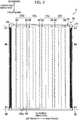
- the nozzles 24 formed in the nozzle plate 20 are divided among four nozzle sets 27 juxtaposed in the scanning direction, as illustrated in Figs. 2 and 3 .
- Each of the four nozzle sets 27 ejects ink in a different color from the others.
- Each nozzle set 27 includes two left and right nozzle rows 28.
- the nozzles 24 in each nozzle row 28 are arranged at a pitch P in the conveying direction.
- the positions of nozzles 24 in the two nozzle rows 28 of each nozzle set 27 are offset from each other in the conveying direction by P/2.
- the nozzles 24 constituting a single nozzle set 27 are arranged in two rows such that their positions in the conveying direction are staggered between rows.
- a nozzle set 27k denotes the nozzle set 27 that ejects black ink.
- the channel member 21 is a single-crystal silicon substrate. As shown in Figs. 2 through 6 , a plurality of pressure chambers 26 is formed in the channel member 21. Each pressure chambers 26 is communication with one of the plurality of nozzles 24. Each of the pressure chambers 26 has a rectangular planar shape that is elongated in the scanning direction. The pressure chambers 26 are arranged in two rows for each ink color, for a total of eight pressure chamber rows, with pressure chambers 26 in each row juxtaposed in the conveying direction at positions corresponding to the nozzles 24.
- the channel member 21 has a bottom surface that is covered by the nozzle plate 20. Further, an outer end of each pressure chamber 26 in the scanning direction corresponding to the same color overlaps one of the nozzles 24 vertically.
- Each pressure chamber 26 has a length L in the scanning direction of approximately 500-1000 ⁇ m, a width W (dimension in the conveying direction) of approximately 65 ⁇ m, and a depth D of approximately 125 ⁇ m (between 50 and 150 ⁇ m).
- the ratio of the depth D to the width W of the pressure chamber 26 in the embodiment is approximately two times (between one and three times).
- the length L of the pressure chamber 26 in the scanning direction is a distance between both inner wall surfaces of the pressure chamber 26 in the scanning direction.
- the width W of the pressure chamber 26 is a distance between both inner wall surfaces of the pressure chamber 26 in the conveying direction.
- a vertical dimension of the pressure chamber 26 varies in different areas of the pressure chamber 26 due to deflection of a vibrating film 30 (described later) formed over a top surface of the pressure chamber 26. Accordingly, the depth D of the pressure chamber 26 described herein designates a distance between a top surface of the nozzle plate 20 and a surface of the vibrating film 30 on the pressure chamber 26 side (bottom surface) in a region between neighboring pressure chambers 26 (a non-deflected area).
- a single vibrating film 30 constituting a component of the piezoelectric actuator 22 described later is arranged on the top surface of the channel member 21 so as to cover the plurality of pressure chambers 26.
- the vibrating film 30 has no particular limitations and may be any insulating film that covers the pressure chambers 26.
- the vibrating film 30 is formed by oxidizing or nitriding a surface of a silicon substrate, for example.
- Ink supply holes 30a are formed in areas of the vibrating film 30 that cover inner ends of the pressure chambers 26 in the scanning direction (the ends opposite the nozzles 24).
- the vibrating film 30 has a thickness E1 of approximately 1-3 ⁇ m.
- the thickness E1 of the vibrating film 30 designates a distance between the surface of the vibrating film 30 on the channel member 21 side (bottom surface) and a surface of the vibrating film 30 opposite the channel member 21 (top surface).
- the actuator device 25 is arranged on the top surface of the channel member 21. As mentioned earlier, the actuator device 25 includes the piezoelectric actuator 22 that includes a plurality of piezoelectric elements 31, the protective member 23, and two COFs 50.
- the piezoelectric actuator 22 is arranged over the entire top surface of the channel member 21. As shown in Figs. 3 and 4 , the piezoelectric actuator 22 includes a plurality of the piezoelectric elements 31 arranged each at a position overlapping a corresponding one of the plurality of pressure chambers 26. The piezoelectric elements 31 configure eight piezoelectric element rows 38. The piezoelectric elements 31 in each piezoelectric element row 38 are juxtaposed in the conveying direction at positions conforming to the positions of the pressure chambers 26. A plurality of drive contacts 46 and two ground contacts 47 are led leftward from the four piezoelectric element rows 38 on the left side. These contacts 46 and 47 are arranged along a left edge of the channel member 21, as illustrated in Figs.
- a plurality of drive contacts 46 and two ground contacts 47 are led rightward from the four piezoelectric element rows 38 on the right side and are arranged along a right edge of the channel member 21.
- a detailed structure of the piezoelectric actuator 22 will be described later.
- the protective member 23 is arranged over a top surface of the piezoelectric actuator 22 so as to cover the piezoelectric elements 31.
- the protective member 23 has eight concave protection areas 23a that individually cover the corresponding eight piezoelectric element rows 38. Note that the protective member 23 does not cover left and right edges of the piezoelectric actuator 22. Consequently, the drive contacts 46 and ground contacts 47 are exposed outside the protective member 23, as shown in Fig. 2 .
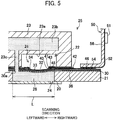
- the protective member 23 also has four reservoirs 23b that are to be connected respectively to the four ink cartridges 17 in the cartridge holder 7. Ink in the reservoirs 23b is supplied to the corresponding pressure chambers 26 along ink supply channels 23c ( Fig. 5 ) and through the ink supply holes 30a formed in the vibrating film 30.
- the COFs 50 shown in Figs. 2-5 are flexible wiring members.
- Each COF 50 has a circuit board 56 formed of an electrically insulating material, such as polyimide film.
- a driver IC 51 is mounted on the circuit board 56.
- One end of each COF 50 is connected to the controller 6 provided in the printer 1 (see Fig. 1 ), while the other end is connected to the corresponding left or right end of the piezoelectric actuator 22.
- each COF 50 includes a plurality of individual wires 52 that are connected to the driver IC 51, and two ground wires 53.
- An individual contact 54 is provided on a leading end of each individual wire 52. The individual contacts 54 connect with corresponding drive contacts 46 on the piezoelectric actuator 22.
- a ground connection contact 55 is provided on a leading end of each ground wire 53.
- the ground connection contacts 55 connect with corresponding ground contacts 47 on the piezoelectric actuator 22.
- the driver IC 51 is configured to output individual drive signals to each of the piezoelectric elements 31 in the piezoelectric actuator 22 via the individual contacts 54 and drive contacts 46.
- the piezoelectric actuator 22 includes, in addition to the vibrating film 30 described above, a common electrode 36 (a plurality of first electrodes 32), piezoelectric films 33, and a plurality of second electrodes 34.
- protective films 40, insulating films 41, and wiring protective films 43 shown in the cross-sectional views of Figs. 5 and 6 have been omitted from Figs. 3 and 4 for simplification.
- the first electrodes 32 are formed in areas on the top surface of the vibrating film 30 opposite the pressure chambers 26. As shown in Fig. 6 , the first electrodes 32 are connected via conductive parts 35 arranged on the top surface of the vibrating film 30 in areas not vertically overlapping the pressure chambers 26. Connecting the plurality of first electrodes 32 via the conductive parts 35 in this way forms the common electrode 36 so as to cover substantially the entire top surface of the vibrating film 30.
- the common electrode 36 is formed of platinum (Pt), for example, and has a thickness of 0.1 ⁇ m, for example.
- the piezoelectric films 33 are formed of a piezoelectric material, such as PZT. Alternatively, the piezoelectric films 33 may be formed of a lead-free piezoelectric material.
- the piezoelectric films 33 have a thickness E2 that is smaller than the thickness E1 of the vibrating film 30, such as 1.0-2.0 ⁇ m (less than or equal to 2.0 ⁇ m).
- the thickness E2 of the piezoelectric films 33 denotes a distance between a surface of the piezoelectric film 33 on the vibrating film 30 side (bottom surface) and a surface of the piezoelectric film 33 on a side opposite the vibrating film 30 (top surface).
- the piezoelectric films 33 are arranged on the top surface of the vibrating film 30 over which the common electrode 36 is formed.
- One piezoelectric film 33 is provided for each pressure chamber row and extends in the conveying direction across the plurality of pressure chambers 26 constituting the pressure chamber row 38. There are eight piezoelectric films 33 in total.
- the second electrodes 34 are arranged on the top surfaces of the piezoelectric films 33 each at a position corresponding to a corresponding one of the pressure chambers 26.
- the second electrodes 34 have a rectangular planar shape that is slightly smaller than the pressure chambers 26 and vertically overlap center regions of the corresponding pressure chambers 26. Unlike the first electrodes 32, the second electrodes 34 are separated from one another. In other words, the second electrodes 34 are individual electrodes provided individually for each of the pressure chambers 26.
- the second electrodes 34 are formed of iridium (Ir) or platinum (Pt), for example.
- the second electrodes 34 has a thickness of 0.1 ⁇ m, for example.
- the second electrodes 34 are formed according to a sputtering method described later and possess compressive stress.
- each piezoelectric film 33 interposed between one first electrode 32 and one second electrode 34 is polarized so that a ratio of (001) orientation to (100) orientation in the piezoelectric film 33 is 50% or greater.
- the orientation ratio in the piezoelectric film 33 is more preferably at least 80%.
- the second electrodes 34 have compressive stress, and the ratio of (001) orientation to (100) orientation in the piezoelectric film 33 is 50% or greater.
- the portions of the vibrating film 30 and piezoelectric films 33 vertically overlapping the pressure chambers 26 are convexly deflected toward the pressure chambers 26 while a potential difference is not produced between the first electrodes 32 and second electrodes 34.
- the vibrating film 30 and piezoelectric films 33 at this time provide a deflection amount T of approximately 450 nm (between 400 and 500 nm).
- the deflection amount T denotes a vertical distance between a border K at which the side wall surface of the pressure chamber 26 meets the vibrating film 30, and a point on the bottom surface of the vibrating film 30 that vertically overlaps a center of the pressure chamber 26 in the conveying direction (see Fig. 6 ).
- the portions of the vibrating film 30 and piezoelectric films 33 vertically overlapping each pressure chamber 26, and the first electrode 32 and second electrode 34 vertically overlapping this portion of the piezoelectric film 33 together form one piezoelectric element 31.
- a plurality of the piezoelectric elements 31 is juxtaposed in the conveying direction in conformance with the juxtaposition of the pressure chambers 26. Accordingly, in conformance with the arrangement of nozzles 24 and pressure chambers 26, the piezoelectric elements 31 configure two piezoelectric element rows 38 for each color of ink, making a total of eight piezoelectric element rows 38.
- a set of piezoelectric elements 31 forming two piezoelectric element rows 38 for one color of ink will be called a piezoelectric element set 39.
- four piezoelectric element sets 39k, 39y, 39c, and 39m corresponding to the four ink colors are juxtaposed in the scanning direction.
- the piezoelectric actuator 22 further includes the protective films 40, the insulating films 41, wires 42, and the wiring protective films 43.
- the protective films 40 are arranged so as to cover the top surfaces of the corresponding piezoelectric films 33, excluding regions corresponding to center portions of the second electrodes 34.
- a primary function of the protective film 40 is to prevent moisture in the air from entering the piezoelectric film 33.
- the protective film 40 is formed of a material having low water permeability.
- the protective film 40 may be formed of an oxide such as alumina (Al 2 O 3 ), silicon oxide (SiO x ), tantalum oxide (TaO x ), or the like; or a nitride such as silicon nitride (SiN).
- the insulating films 41 are formed over the tops of respective protective films 40. While there are no particular limitations on the type of material used to form the insulating film 41, the insulating film 41 may be formed of silicon dioxide (SiO 2 ), for example. The insulating film 41 serves to enhance the insulating properties between the wires 42 (described next) connected to the second electrodes 34, and the common electrode 36.
- a plurality of the wires 42 is formed on the insulating films 41.
- the wires 42 are lead out from the second electrodes 34 in the plurality of piezoelectric elements 31.
- the wires 42 are formed of aluminum (Al), for example. As shown in Fig. 5 , one end of each wire 42 is arranged in a position overlapping an end of the corresponding second electrode 34 on top of the piezoelectric film 33 and is electrically connected to the corresponding second electrode 34 by a through conductive part 48 penetrating the protective film 40 and insulating film 41.
- the wires 42 can be divided into those that extend leftward from the piezoelectric elements 31 and those that extend rightward. Specifically, among the four piezoelectric element sets 39 shown in Fig. 3 , the wires 42 extend rightward from the piezoelectric elements 31 constituting the two piezoelectric element sets 39k and 39y on the right side and extend leftward from the piezoelectric elements 31 constituting the two piezoelectric element sets 39c and 39m on the left side.
- the drive contacts 46 are provided each on another end of the wire 42 opposite the end connected to the second electrode 34.
- a plurality of the drive contacts 46 is arranged in a row extending in the conveying direction on both the left and right edges of the piezoelectric actuator 22.
- the nozzles 24 constituting a nozzle set 27 for one color are arranged at a pitch of 600 dpi (equivalent to 42 ⁇ m).
- the wires 42 are drawn out either leftward or rightward from the piezoelectric elements 31 corresponding to the nozzle sets 27 for two colors. Consequently, the drive contacts 46 on both the left and right edges of the piezoelectric actuator 22 are arranged at an extremely narrow pitch that is half the pitch of the nozzles 24 in a single nozzle set 27, or approximately 21 ⁇ m.
- ground contacts 47 are arranged on ends of each row of drive contacts 46, with one on the front end and one on the rear end.
- One ground contact 47 has a greater contact area than one drive contact 46.
- the ground contacts 47 are connected to the common electrode 36 through conductive parts (not shown) penetrating the protective films 40 and insulating films 41 directly beneath the ground contacts 47.
- the drive contacts 46 and ground contacts 47 arranged on the left and right edges of the piezoelectric actuator 22 are exposed outside the protective member 23.
- the COFs 50 are also bonded to the left and right edges of the piezoelectric actuator 22.
- the drive contacts 46 are connected to the driver IC 51 of the corresponding COF 50 via the individual contacts 54 and individual wires 52, and drive signals are supplied to the drive contacts 46 from the driver IC 51.
- the driver IC 51 can selectively apply either a ground potential or a prescribed drive potential (approximately 20V, for example) to each of the second electrodes 34 individually.
- a ground potential is applied by connecting the ground contacts 47 to the ground connection contacts 55 of the COFs 50.
- the wiring protective films 43 are arranged so as to cover the wires 42.
- the wiring protective films 43 improve the insulation between adjacent wires 42.
- the wiring protective films 43 also suppress oxidation of the wiring material (aluminum, etc.) constituting the wires 42.
- the wiring protective films 43 are formed of silicon nitride (SiN x ), for example.
- the second electrodes 34 are exposed in the protective films 40, insulating films 41, and wiring protective films 43 in the embodiment, as illustrated in Figs. 5 and 6 .
- the protective films 40, insulating films 41, and wiring protective films 43 are configured so as not to hinder deformation of the piezoelectric films 33.
- the second electrodes 34 in all piezoelectric elements 31 of the piezoelectric actuator 22 are maintained at a drive potential.
- the potential difference between the first electrodes 32 and second electrodes 34 produces an electric field along a thickness of the piezoelectric film 33 that causes the piezoelectric film 33 to contract in a direction orthogonal to a thickness direction thereof. Consequently, the portions of the vibrating film 30 and piezoelectric films 33 that vertically overlap the pressure chambers 26 deflect convexly toward the pressure chamber 26 side (downward), and the amount of this deflection is greater than when a potential difference is not produced between the first electrodes 32 and second electrodes 34.
- the piezoelectric films 33 of the embodiment are thin, having a thickness of approximately 1.0-2.0 ⁇ m, a large electric field is generated in the piezoelectric films 33, producing a large deflection amount in the vibrating film 30 and piezoelectric films 33.
- the potential of the second electrode 34 in the piezoelectric element 31 corresponding to that nozzle 24 is temporarily switched to the ground potential and then returned to the drive potential.
- the first electrode 32 and second electrode 34 have the same potential, eliminating the electric field and thereby reducing the amount of deflection in the vibrating film 30 and piezoelectric film 33.
- the deflection amount of the vibrating film 30 and piezoelectric film 33 increases, reducing a capacity of the pressure chamber 26. The reduction in capacity increases the pressure of ink in the pressure chamber 26, causing ink to be ejected from the nozzle 24 that communicates with the pressure chamber 26.
- crosstalk displacement crosstalk and ejection crosstalk
- the drive of the piezoelectric element 31 corresponding to a certain pressure chamber 26 affects the ejection speed of ink from a nozzle 24 communicating with a separate pressure chamber 26. This phenomenon of crosstalk will be described next in greater detail.
- one pressure chamber 26 will be called a pressure chamber 26A
- the piezoelectric element 31 corresponding to the pressure chamber 26A will be called a piezoelectric element 31A, as illustrated in Fig. 6 .
- the two pressure chambers 26 adjacent to the pressure chamber 26A on both sides in the conveying direction will be called pressure chambers 26B
- the piezoelectric elements 31 corresponding to the pressure chambers 26B will be called piezoelectric elements 31B.
- the portions of the vibrating film 30 forming the piezoelectric elements 31B are deflected, as described above. While the portions of the vibrating film 30 forming the piezoelectric elements 31B are deflected, tensile stress is generated in the portion of the vibrating film 30 forming the piezoelectric element 31A. This tensile stress causes the portion of the vibrating film 30 forming the piezoelectric element 31A to elongate and urges the portions of the vibrating film 30 and piezoelectric film 33 forming the piezoelectric element 31A to deform convexly toward the pressure chambers 26A.
- partitioning walls 21a of the channel member 21 that separate neighboring pressure chambers 26 have a narrow dimension in the conveying direction.
- the partitioning walls 21a between the pressure chamber 26A and pressure chambers 26B are susceptible to collapsing toward the pressure chamber 26B side from the pull of the vibrating film 30.
- the portion of the vibrating film 30 forming the piezoelectric element 31A tends to deform in a direction toward a flat state.
- the portions of the vibrating film 30 and piezoelectric film 33 forming the piezoelectric elements 31 deflect convexly toward the side opposite the pressure chambers 26 while a potential difference is not being produced between the first electrodes 32 and second electrodes 34.
- the portions of the vibrating film 30 and piezoelectric film 33 forming the piezoelectric element 31A are inclined to deform in a direction to be convex toward the pressure chamber 26A owing to the tensile stress described above.
- the portions of the vibrating film 30 and piezoelectric film 33 forming the piezoelectric element 31A are inclined to deform in a direction for flattening out (the direction for forming a convex shape on the pressure chamber 26 side).
- the direction in which the portions of the vibrating film 30 and piezoelectric film 33 that form the piezoelectric element 31A are inclined to deform due to the tensile stress and the direction in which the portions of the vibrating film 30 and piezoelectric film 33 forming the piezoelectric element 31A are inclined to deform when the partitioning walls 21a are prone to collapse are the same direction. Consequently, forces tending to deform these parts are added together when driving the piezoelectric actuator 22 in this case, thereby increasing displacement crosstalk.
- the portions of the vibrating film 30 and piezoelectric film 33 forming the piezoelectric elements 31 deflect convexly toward the pressure chamber 26 side while a potential difference is not being produced between the first electrodes 32 and second electrodes 34.
- the portions of the vibrating film 30 and piezoelectric film 33 forming the piezoelectric element 31A are inclined to be deformed by the tensile stress described above in a direction for forming a convex shape on the pressure chamber 26 side.
- the portions of the vibrating film 30 and piezoelectric film 33 forming the piezoelectric element 31A are inclined to deform in a direction for flattening out (a direction toward forming a convex shape on the side opposite the pressure chamber 26).
- the direction in which the portions of the vibrating film 30 and piezoelectric film 33 forming the piezoelectric element 31A are inclined to deform due to the tensile stress is opposite the direction in which the portions of the vibrating film 30 and piezoelectric film 33 forming the piezoelectric element 31A are inclined to deform when the partitioning walls 21a are prone to collapse.
- the forces acting to deform these parts cancel each other in this case, reducing displacement crosstalk.
- the partitioning walls 21a in the conveying direction are shorter and the depth of the pressure chambers 26 is greater (the vertical length of the partitioning walls 21a is longer), the partitioning walls 21a are more susceptible to deformation (have greater compliance) in response to fluctuations in ink pressure in the pressure chambers 26. Accordingly, the partitioning walls 21a having higher compliance is more likely to deform when the piezoelectric element 31 is driven as described above to apply pressure to ink in a pressure chamber 26, and the pressure fluctuation caused by the deformation of the partitioning walls 21a is transmitted to other pressure chambers 26.
- ink pressure in the pressure chamber 26A and ink pressure in the pressure chambers 26B will fluctuate at the same time, inhibiting deformation of the partitioning walls 21a and thus inhibiting the transmission of pressure fluctuations described above.
- the piezoelectric element 31B is not driven at the same time as the piezoelectric element 31A is driven, pressure fluctuations in the pressure chamber 26A are readily transmitted to the pressure chamber 26B. This difference in how pressure fluctuations are transmitted together with the displacement crosstalk described above cause variations in the speed at which ink is ejected from the nozzles 24 called ejection crosstalk.
- the inkjet head 4 can be manufactured according to a procedure following a flowchart in Fig. 7 , for example.
- the vibrating film 30 is formed on a silicon substrate, which will become the channel member 21.
- the vibrating film 30 is formed by oxidizing or nitriding the surface of the silicon substrate.
- an electrode film that will serve as the common electrode 36 (the first electrodes 32) is formed over the top surface of the vibrating film 30.
- a piezoelectric material film that will become the piezoelectric film 33 is formed over the top surface of the electrode film.
- the piezoelectric material film is formed according to the sol-gel process. More specifically, the piezoelectric material film is formed by repeatedly performing steps for forming the piezoelectric material by spin coating a solution of the material and then crystalizing the piezoelectric material through an annealing process.
- an electrode film that will become the second electrodes 34 is formed on the top surface of the piezoelectric material film.
- This electrode film is formed by sputtering or the like, at which time the conditions are controlled so that the electrode film will possess compressive stress.
- the common electrode 36 (first electrodes 32), piezoelectric films 33, and second electrodes 34 are formed by patterning the electrode film and piezoelectric film formed in the preceding steps using photolithography, dry etching, and the like.
- the protective films 40, insulating films 41, wires 42, wiring protective films 43, drive contacts 46, and ground contacts 47 are sequentially formed in S106 and the protective member 23 is bonded to the silicon substrate in S107.
- the plurality of pressure chambers 26 is formed by first polishing the silicon substrate to a thickness suited to the depth D of the pressure chambers 26 and subsequently wet etching or dry etching the silicon substrate from the side opposite the protective member 23. After the pressure chambers 26 are formed in the silicon substrate, the portions of the vibrating film 30 and piezoelectric films 33 vertically overlapping the pressure chambers 26 are no longer restrained by the silicon substrate. At the same time, the second electrodes 34 possess compressive stress, as described above. The compressive stress in the second electrodes 34 causes the portions of the vibrating film 30 and piezoelectric film 33 vertically overlapping the pressure chambers 26 to deflect convexly toward the side opposite the pressure chambers 26, as illustrated in Fig. 8 .
- the nozzle plate 20 having the plurality of nozzles 24 formed therein is bonded to the silicon substrate.
- a water-repellent film may be formed over the surface of the nozzle plate 20 on the side opposite the channel member 21.
- a dicing process is performed to cut the silicon substrate down to a size suitable for the channel member 21.
- a polarizing process is performed for polarizing the piezoelectric films 33 by applying a voltage across the first electrodes 32 and second electrodes 34 under high temperatures.
- the piezoelectric films 33 have a (001) preferential orientation with a ratio of (001) orientation to (100) orientation of at least 50% and preferably 80% or greater.
- the polarizing process in S111 may be performed prior to the dicing process of S110 or following the COF 50 bonding process of S112.
- Examples A1-A11 and a comparative example A are results of experiments on displacement crosstalk.
- the amount of deflection in the vibrating film 30 and piezoelectric film 33 while a potential difference was not produced between the first electrode 32 and second electrode 34 was varied among the examples A1-A11 and the comparative example A.
- Table 1 shows a relationship between the deflection amount T described above and displacement crosstalk (displacement CT in the table) for the examples A1-A11 and the comparative example A.
- [Table 1] Deflection Amount T (nm) Displacement CT (%) Comparative Example A -167 14.0
- Example A6 300 11.0
- Example A11 596 1.6
- a positive value for the deflection amount T indicates convex deflection toward the pressure chambers 26, while a negative value indicates convex deflection toward the side opposite the pressure chambers 26.
- the values for displacement crosstalk in Table 1 are all positive values, but this indicates that displacement when neighboring piezoelectric elements 31 are driven simultaneously is greater than displacement when neighboring piezoelectric elements 31 are not driven simultaneously.
- Examples B1-B6 and comparative examples B1-B3 are the results of experiments on ejection crosstalk.
- the amount of deflection T in the vibrating film 30 and piezoelectric films 33 while a potential difference was not produced between the first electrode 32 and second electrode 34 was varied among the examples B1-B6 and the comparative examples B1-B3.
- Table 2 shows a relationship between the deflection amount T and ejection crosstalk (ejection CT in the table) for each example.
- a positive value for the deflection amount T indicates convex deflection toward the pressure chamber 26 side, while a negative value indicates convex deflection toward the side opposite the pressure chambers 26.
- a positive value for ejection crosstalk in Table 2 indicates that the ejection speed is faster when neighboring piezoelectric elements 31 are driven simultaneously than when neighboring piezoelectric elements 31 are not driven simultaneously, and a negative value indicates that the ejection speed is slower when neighboring piezoelectric elements 31 are driven simultaneously than when neighboring piezoelectric elements 31 are not driven simultaneously.
- the deflection amount T in the examples A1-A11 and B1-B6 are all less than or equal to 1% the width W of the pressure chamber 26 (less than or equal to approximately 650 nm).
- crosstalk can be kept sufficiently low (no greater than 12% for displacement crosstalk and no greater than 16% for ejection crosstalk) when the deflection amount T is no greater than 1% the width W of the pressure chamber 26.
- X-ray diffraction was performed on a sample with deflection toward the pressure chamber side produced through the same polarization process used for the example A1 and a sample with deflection toward the side opposite the pressure chamber side equivalent to the comparative example A to evaluate the ratio of (001) orientation to (100) orientation based on the intensity of the (400) and (004) peaks in Miller indices.
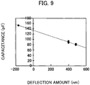
- Fig. 9 is a graph plotting deflection amounts in relation to capacitance. Capacitance drops as the amount of deflection increases toward the pressure chamber side, indicating that the ratio of (001) orientation increases as the amount of deflection increases. Under the conditions of the example A1, the ratio of (001) orientation is approximately 50% with a deflection amount of 276 nm. This ratio increases further under conditions with larger deflection amounts that are more suitable for reducing crosstalk.
- the piezoelectric films 33 possess tensile stress that tends to produce (100) orientation. However, by polarizing the piezoelectric films 33 in the embodiment, a ratio of at least 50% (001) orientation to (100) orientation is achieved. Therefore, the piezoelectric films 33 have good piezoelectric properties.
- the piezoelectric films 33 can be contracted so that the vibrating film 30 and piezoelectric films 33 deflect convexly toward the pressure chamber 26 side.
- crosstalk is less likely to occur when the vibrating film 30 and piezoelectric film 33 deflect convexly toward the pressure chamber 26 side than when they deflect convexly toward the side opposite the pressure chamber 26 side.
- the piezoelectric properties of the piezoelectric films 33 can be sufficiently improved by further increasing the ratio of (001) orientation to (100) orientation in the piezoelectric films 33 to 80% or greater.
- piezoelectric films 33 formed through this sol-gel process generally tend to have (100) orientation. Therefore, it is important to improve the ratio of (001) orientation to (100) orientation by polarizing the piezoelectric films 33 as described above.
- the piezoelectric film 33 can be formed as thin as 2 ⁇ m or less, thereby increasing the strength of the electric field produced in the piezoelectric film 33 when a voltage is applied across the first electrodes 32 and second electrodes 34 and, hence, increasing the amount of displacement T produced in the piezoelectric film 33.
- ratio of depth D to width W of the pressure chamber 26 is approximately two times, a ratio between one time and three times can achieve the same effects of reducing crosstalk illustrated in the above examples.
- depth D of the pressure chamber 26 is approximately 125 ⁇ m in the embodiment, a depth in a range from 50-180 ⁇ m can achieve the same effects of reducing crosstalk illustrated in the above examples.
- the deflection amount T is controlled to be no greater than 1% of the width W of the pressure chamber 26 in the embodiment.
- this technique can maximize the amount of deformation T in the vibrating film 30 and piezoelectric film 33 when a voltage is applied across the first electrode 32 and second electrode 34, while deflecting the vibrating films 30 and piezoelectric film 33 convexly toward the pressure chamber 26 side to reduce the likelihood of crosstalk.
- the deflection amount T described above is approximately 450 nm in the embodiment, the deflection amount T may be in a range from 400-500 nm. As shown in the above examples, this technique can maximize the amount of deformation T in the vibrating film 30 and piezoelectric film 33 when a voltage is applied across the first electrodes 32 and second electrodes 34, while deflecting the vibrating film 30 and piezoelectric film 33 convexly toward the pressure chamber 26 side to reduce the likelihood of crosstalk.
- the deflection amount T of the vibrating film 30 and piezoelectric film 33 when a potential difference is not being produced between the first electrode 32 and second electrode 34 is between 400 and 500 nm, but the deflection amount T may be less than 400 nm or greater than 500 nm.
- the deflection amount T of the vibrating film 30 and piezoelectric film 33 while a potential difference is not being produced between the first electrode 32 and second electrode 34 is no greater than 1% of the width W of the pressure chamber 26, but the deflection amount T may be greater than 1% of the width W of the pressure chamber 26.
- the depth D of the pressure chamber 26 is between 50 and 150 ⁇ m, but the depth D of the pressure chamber 26 may be less than 50 ⁇ m or greater than 150 ⁇ m.
- the ratio of the depth D to the width W of the pressure chamber 26 is between one and three times, but the ratio of the depth D to the width W of the pressure chamber 26 may be less than one time or greater than three times.
- the thickness E2 of the piezoelectric film 33 is set to 2 ⁇ m or less, which is thinner than the thickness E1 of the vibrating film 30.
- the present disclosure is not limited to this configuration.
- the thickness E2 of the piezoelectric film 33 may be set greater than 2 ⁇ m, provided that the thickness E2 is thinner than the thickness E1 of the vibrating film 30.
- the thickness E2 of the piezoelectric film 33 may be set greater than or equal to the thickness E1 of the vibrating film 30.
- the piezoelectric films 33 are formed according to the sol-gel process, but the piezoelectric films 33 may be formed according to another method, such as sputtering.
- the common electrode 36 is formed between the piezoelectric films 33 and vibrating film 30 by linking neighboring first electrodes 32 through conductive parts 35, and the second electrodes 34 arranged on the top surfaces of the piezoelectric films 33 are individual electrodes provided for each individual pressure chamber 26.
- the first electrodes 32 disposed between the piezoelectric films 33 and vibrating film 30 may instead be individual electrodes provided for each individual pressure chamber 26, and a common electrode may be formed by linking neighboring second electrodes 34 arranged on the top surfaces of the piezoelectric films 33.
- the present disclosure may be applied to a liquid ejection head that ejects a liquid other than ink, such as a liquefied metal or resin.
- the inkjet head 4 is an example of a liquid ejection head.
- the nozzles 24 are an example of nozzles.
- the channel member 21 is an example of a channel member.
- the pressure chambers 26 are an example of a plurality of pressure chambers.
- the piezoelectric elements 31 are an example of a plurality of piezoelectric elements.
- the vibrating film 30 (a portion thereof corresponding to each pressure chamber 26) is an example of a vibrating film.
- the piezoelectric film 33 (a portion thereof corresponding to each pressure chamber 26) is an example of a piezoelectric film.
- the first electrodes 32 are an example of a first electrode.
- the second electrodes 34 are an example of a second electrode.
Landscapes
- Engineering & Computer Science (AREA)
- Manufacturing & Machinery (AREA)
- Particle Formation And Scattering Control In Inkjet Printers (AREA)
Abstract
Description
- The present disclosure relates to a liquid ejection head that ejects liquid from nozzles.
- As a conventional liquid ejection head for ejecting liquid from nozzles, Japanese Patent Application Publication No.
2000-094688 - The crystal orientation in lead zirconate titanate (PZT) having a perovskite structure expressed with the chemical formula ABO3 has been known to greatly influence the piezoelectric property of the material. This piezoelectric property generates strain in the crystals in response to an applied voltage. Obtaining thin films preferentially oriented along the c-axis, i.e., (001)-oriented, particularly in PZT having a tetragonal perovskite structure is thought to be effective for producing strong piezoelectric properties. a-axis, i.e., (100) preferentially oriented thin films and the like may produce great deformation when a strong electric field is applied to change the orientation of the c-axis from one parallel to a substrate surface to one perpendicular to the surface, but have been problematic in achieving stable driving since the amount of their deformation tends to be irregular.
- With the conventional technology described above, tensile stress is generated in the piezoelectric film because the upper electrode film has compressive stress and, thus, the piezoelectric film tends to be (100)-oriented. A (100) orientation is also common in piezoelectric films formed according to the sol-gel process used in the conventional technology. However, as described above, highly (100)-oriented piezoelectric thin films do not tend to produce good piezoelectric properties when voltage is applied across their upper and lower electrode films.
- Further, the elastic film and vibrating film in the conventional technology are deflected convexly toward the side opposite the pressure chambers by the compressive stress in the upper electrode film. However, inkjet recording heads having an elastic film and a vibrating film deflected convexly toward the side opposite the pressure chambers is susceptible to producing crosstalk during driving, as will be described later.
- In view of the foregoing, it is an object of the disclosure to provide a liquid ejection head that achieves good piezoelectric properties while inhibiting crosstalk.
- In order to attain the above and other objects, according to one aspect, the disclosure provides a liquid ejection head including a plurality of nozzles, a channel member, and a plurality of piezoelectric elements. The channel member includes a plurality of pressure chambers each in communication with a corresponding one of the plurality of nozzles. Each of the plurality of piezoelectric elements is provided for a corresponding one of the plurality of pressure chambers. Each of the plurality of piezoelectric elements includes: a vibrating film covering the corresponding pressure chamber; a piezoelectric film positioned opposite to the corresponding pressure chamber with respect to the vibrating film; a first electrode interposed between the vibrating film and the piezoelectric film; and a second electrode positioned opposite to the vibrating film with respect to the piezoelectric film. The vibrating film, the piezoelectric film, the first electrode, and the second electrode vertically overlap the corresponding pressure chamber. The second electrode has compressive stress. The piezoelectric film has a ratio of (001) orientation to (100) orientation that is equal to or greater than 50%. The vibrating film and the piezoelectric film are deflected convexly toward the corresponding pressure chamber while no potential difference is being produced between the first electrode and the second electrode.
- With this structure according to the one aspect, although the piezoelectric film possesses tensile stress that tends to produce (100) orientation due to the compressive stress of the second electrode, the ratio of at least 50% (001) orientation to (100) orientation is achieved by polarizing the piezoelectric film. Therefore, the piezoelectric film has good piezoelectric property.
- Further, by polarizing the piezoelectric film to increase the ratio of (001) orientation to (100) orientation, the piezoelectric film can be contracted so that the vibrating film and piezoelectric film deflect convexly toward the corresponding pressure chamber. With this structure, crosstalk is less likely to occur when the vibrating film and piezoelectric film deflect convexly toward the corresponding pressure chamber than when they deflect convexly in a direction away from the corresponding pressure chamber.
- In the liquid ejection head according to the one aspect, preferably, the piezoelectric film is a film formed according to sol-gel process.
- Piezoelectric films formed through the sol-gel process generally tend to have (100) orientation. Therefore, it is important to improve the ratio of (001) orientation to (100) orientation by polarizing the piezoelectric film. When using the sol-gel process, the piezoelectric film can be formed as thin as 2 µm or less, thereby increasing the strength of the electric field produced in the piezoelectric film when a voltage is applied across the first electrode and second electrodes. Hence, the amount of displacement produced in the piezoelectric film can be increased.
- In this liquid ejection head, it is further preferable that the piezoelectric film has a thickness smaller than a thickness of the vibrating film. More specifically, the thicknessof t hepi ezoelectricf ilmm ay bepr eferablyl esst han or equalt o 2.0 µm.
- This structure can reduce the likelihood of crosstalk.
- Further, in the liquid ejection head according to the one aspect, it is preferable that each of the pressure chambers defines a depth and a width, a ratio of the depth to the width being between one time and three times.
- With the ratio between one time and three times, crosstalk is less likely to occur than otherwise.
- Alternatively, in the liquid ejection head according to the one aspect, it is preferable that each of the pressure chambers defines a depth that is between 50 µm and 150 µm.
- With this structure as well, crosstalk is less likely to occur than otherwise.
- Further, in the liquid ejection head according to the one aspect, it is preferable that the vibrating film and the piezoelectric film are deflected convexly toward the corresponding pressure chamber to provide a deflection amount while no potential difference is being produced between the first electrode and the second electrode, the deflection amount being less than or equal to 1% of the width of the corresponding pressure chamber.
- With this structure, the amount of deformation in the vibrating film and piezoelectric film can be maximized when a voltage is applied across the first electrode and the second electrode, while the likelihood of crosstalk is reduced.
- Alternatively, in the liquid ejection head according to the one aspect, it is preferable that the vibrating film and the piezoelectric film are deflected convexly toward the corresponding pressure chamber to provide a deflection amount while no potential difference is being produced between the first electrode and the second electrode, the deflection amount being in a range from 400-500 nm.
- With this structure, the amount of deformation in the vibrating film and piezoelectric film can be maximized when a voltage is applied across the first electrode and the second electrode, while the likelihood of crosstalk is reduced.
- Further, in the liquid ejection head according to the one aspect, preferably, the piezoelectric film is polarized such that the ratio of (001) orientation to (100) orientation in the piezoelectric film is 80% or greater.
- By increasing the ratio of (001) orientation to (100) orientation in the piezoelectric film to 80% or greater, piezoelectric property of the piezoelectric film can be further sufficiently improved.
- The particular features and advantages of the embodiment(s) as well as other objects will become apparent from the following description taken in connection with the accompanying drawings, in which:
-
Fig. 1 is a schematic plan view of a printer according to one embodiment of the disclosure; -
Fig. 2 is a plan view of an inkjet head of the printer according to the embodiment; -
Fig. 3 is a partially enlarged view of a rear end portion of the inkjet head ofFig. 2 ; -
Fig. 4 is an enlarged view of a portion A enclosed by a phantom line inFig. 3 ; -
Fig. 5 is a cross-sectional view of a portion taken along a line V-V inFig. 4 ; -
Fig. 6 is a cross-sectional view of a portion taken along a line VI-VI inFig. 4 ; -
Fig. 7 is a flowchart illustrating steps in manufacturing the inkjet head according to a second embodiment; -
Fig. 8 is a view corresponding to the portion ofFig. 6 in a state where pressure chambers are formed in a channel member of the inkjet head of the according to the embodiment; and -
Fig. 9 is a graph illustrating a relationship between deflection and electrostatic capacity. - Hereinafter, one embodiment of the disclosure will be described while referring to
Figs. 1 through 9 . - As shown in
Fig. 1 , a printer 1 according to the embodiment includes a platen 2, acarriage 3, aninkjet head 4, aconveying mechanism 5, a controller 6, and acartridge holder 7. - The
carriage 3 is mounted on twoguide rails carriage 3 is connected to acarriage drive motor 15, via anendless belt 14. Thecarriage 3 is configured to be driven by thecarriage drive motor 15 to reciprocate in the scanning direction above arecording sheet 100 supported on the platen 2. In the following description, a leftward direction and a rightward direction will be defined as shown inFig. 1 based on the scanning direction. - The
inkjet head 4 is mounted on thecarriage 3. A plurality of nozzles 24 (seeFigs. 2-6 ) is formed in a bottom of theinkjet head 4. Theinkjet head 4 is configured to move together with thecarriage 3 in the scanning direction while ejecting ink from thenozzles 24 toward therecording sheet 100 supported on the platen 2. Thecartridge holder 7 can accommodate fourink cartridges 17 accommodating ink in the four colors black, yellow, cyan, and magenta, respectively. Ink is supplied from each of theink cartridges 17 to theinkjet head 4 through a corresponding tube (not shown). - The conveying
mechanism 5 includes two conveyingrollers recording sheet 100 over the platen 2 in a conveying direction orthogonal to the scanning direction. In the following description, a frontward direction and a rearward direction are defined as shown inFig. 1 based on the conveying direction. - The controller 6 is configured to control operations of the
inkjet head 4,carriage drive motor 15, and the like based on print commands inputted from a personal computer or other external device in order to print images and the like on therecording sheet 100. - Next, a structure of the
inkjet head 4 will be described in detail with reference toFigs. 2 through 6 . Note that aprotective member 23 shown inFig. 2 has been omitted fromFigs. 3 and4 . - The
inkjet head 4 of the embodiment is configured to eject ink in all of the four colors described above (black, yellow, cyan, and magenta). As shown inFigs. 2 through 6 , theinkjet head 4 includes anozzle plate 20, achannel member 21, and anactuator device 25 that includes apiezoelectric actuator 22. Note that theactuator device 25 in the embodiment does not simply designate thepiezoelectric actuator 22, but conceptually includes theprotective member 23 and wiring members called chip-on-films (COFs) 50 arranged on top of thepiezoelectric actuator 22. - The
nozzle plate 20 is formed of silicon, for example. Thenozzles 24 are formed in thenozzle plate 20 in rows extending in the conveying direction. - More specifically, the
nozzles 24 formed in thenozzle plate 20 are divided among four nozzle sets 27 juxtaposed in the scanning direction, as illustrated inFigs. 2 and3 . Each of the four nozzle sets 27 ejects ink in a different color from the others. Each nozzle set 27 includes two left andright nozzle rows 28. Thenozzles 24 in eachnozzle row 28 are arranged at a pitch P in the conveying direction. Further, the positions ofnozzles 24 in the twonozzle rows 28 of each nozzle set 27 are offset from each other in the conveying direction by P/2. In other words, thenozzles 24 constituting a single nozzle set 27 are arranged in two rows such that their positions in the conveying direction are staggered between rows. - When appropriate in the following description, one of the symbols "k" denoting black, "y" denoting yellow, "c" denoting cyan, and "m" denoting magenta will be appended to reference numerals assigned to components of the
inkjet head 4 that are associated with the corresponding ink color black (K), yellow (Y), cyan (C), and magenta (M). For example, anozzle set 27k denotes the nozzle set 27 that ejects black ink. - The
channel member 21 is a single-crystal silicon substrate. As shown inFigs. 2 through 6 , a plurality ofpressure chambers 26 is formed in thechannel member 21. Eachpressure chambers 26 is communication with one of the plurality ofnozzles 24. Each of thepressure chambers 26 has a rectangular planar shape that is elongated in the scanning direction. Thepressure chambers 26 are arranged in two rows for each ink color, for a total of eight pressure chamber rows, withpressure chambers 26 in each row juxtaposed in the conveying direction at positions corresponding to thenozzles 24. Thechannel member 21 has a bottom surface that is covered by thenozzle plate 20. Further, an outer end of eachpressure chamber 26 in the scanning direction corresponding to the same color overlaps one of thenozzles 24 vertically. - Each
pressure chamber 26 has a length L in the scanning direction of approximately 500-1000 µm, a width W (dimension in the conveying direction) of approximately 65 µm, and a depth D of approximately 125 µm (between 50 and 150 µm). Thus, the ratio of the depth D to the width W of thepressure chamber 26 in the embodiment is approximately two times (between one and three times). - Here, the length L of the
pressure chamber 26 in the scanning direction is a distance between both inner wall surfaces of thepressure chamber 26 in the scanning direction. Further, the width W of thepressure chamber 26 is a distance between both inner wall surfaces of thepressure chamber 26 in the conveying direction. A vertical dimension of thepressure chamber 26 varies in different areas of thepressure chamber 26 due to deflection of a vibrating film 30 (described later) formed over a top surface of thepressure chamber 26. Accordingly, the depth D of thepressure chamber 26 described herein designates a distance between a top surface of thenozzle plate 20 and a surface of the vibratingfilm 30 on thepressure chamber 26 side (bottom surface) in a region between neighboring pressure chambers 26 (a non-deflected area). - Note that a single vibrating
film 30 constituting a component of thepiezoelectric actuator 22 described later is arranged on the top surface of thechannel member 21 so as to cover the plurality ofpressure chambers 26. The vibratingfilm 30 has no particular limitations and may be any insulating film that covers thepressure chambers 26. In the present embodiment, the vibratingfilm 30 is formed by oxidizing or nitriding a surface of a silicon substrate, for example.Ink supply holes 30a are formed in areas of the vibratingfilm 30 that cover inner ends of thepressure chambers 26 in the scanning direction (the ends opposite the nozzles 24). The vibratingfilm 30 has a thickness E1 of approximately 1-3 µm. Here, the thickness E1 of the vibratingfilm 30 designates a distance between the surface of the vibratingfilm 30 on thechannel member 21 side (bottom surface) and a surface of the vibratingfilm 30 opposite the channel member 21 (top surface). - The
actuator device 25 is arranged on the top surface of thechannel member 21. As mentioned earlier, theactuator device 25 includes thepiezoelectric actuator 22 that includes a plurality ofpiezoelectric elements 31, theprotective member 23, and twoCOFs 50. - The
piezoelectric actuator 22 is arranged over the entire top surface of thechannel member 21. As shown inFigs. 3 and4 , thepiezoelectric actuator 22 includes a plurality of thepiezoelectric elements 31 arranged each at a position overlapping a corresponding one of the plurality ofpressure chambers 26. Thepiezoelectric elements 31 configure eightpiezoelectric element rows 38. Thepiezoelectric elements 31 in eachpiezoelectric element row 38 are juxtaposed in the conveying direction at positions conforming to the positions of thepressure chambers 26. A plurality ofdrive contacts 46 and twoground contacts 47 are led leftward from the fourpiezoelectric element rows 38 on the left side. Thesecontacts channel member 21, as illustrated inFigs. 2 and3 . Similarly, a plurality ofdrive contacts 46 and twoground contacts 47 are led rightward from the fourpiezoelectric element rows 38 on the right side and are arranged along a right edge of thechannel member 21. A detailed structure of thepiezoelectric actuator 22 will be described later. - The
protective member 23 is arranged over a top surface of thepiezoelectric actuator 22 so as to cover thepiezoelectric elements 31. Specifically, theprotective member 23 has eightconcave protection areas 23a that individually cover the corresponding eightpiezoelectric element rows 38. Note that theprotective member 23 does not cover left and right edges of thepiezoelectric actuator 22. Consequently, thedrive contacts 46 andground contacts 47 are exposed outside theprotective member 23, as shown inFig. 2 . Theprotective member 23 also has fourreservoirs 23b that are to be connected respectively to the fourink cartridges 17 in thecartridge holder 7. Ink in thereservoirs 23b is supplied to thecorresponding pressure chambers 26 alongink supply channels 23c (Fig. 5 ) and through theink supply holes 30a formed in the vibratingfilm 30. - The
COFs 50 shown inFigs. 2-5 are flexible wiring members. EachCOF 50 has acircuit board 56 formed of an electrically insulating material, such as polyimide film. Adriver IC 51 is mounted on thecircuit board 56. One end of eachCOF 50 is connected to the controller 6 provided in the printer 1 (seeFig. 1 ), while the other end is connected to the corresponding left or right end of thepiezoelectric actuator 22. As shown inFig. 4 , eachCOF 50 includes a plurality ofindividual wires 52 that are connected to thedriver IC 51, and twoground wires 53. Anindividual contact 54 is provided on a leading end of eachindividual wire 52. Theindividual contacts 54 connect withcorresponding drive contacts 46 on thepiezoelectric actuator 22. Aground connection contact 55 is provided on a leading end of eachground wire 53. Theground connection contacts 55 connect withcorresponding ground contacts 47 on thepiezoelectric actuator 22. Thedriver IC 51 is configured to output individual drive signals to each of thepiezoelectric elements 31 in thepiezoelectric actuator 22 via theindividual contacts 54 and drivecontacts 46. - Next, the
piezoelectric actuator 22 will be described in greater detail. As shown inFigs. 2 through 6 , thepiezoelectric actuator 22 includes, in addition to the vibratingfilm 30 described above, a common electrode 36 (a plurality of first electrodes 32),piezoelectric films 33, and a plurality ofsecond electrodes 34. Note thatprotective films 40, insulatingfilms 41, and wiringprotective films 43 shown in the cross-sectional views ofFigs. 5 and6 have been omitted fromFigs. 3 and4 for simplification. - As shown in
Figs. 5 and6 , thefirst electrodes 32 are formed in areas on the top surface of the vibratingfilm 30 opposite thepressure chambers 26. As shown inFig. 6 , thefirst electrodes 32 are connected viaconductive parts 35 arranged on the top surface of the vibratingfilm 30 in areas not vertically overlapping thepressure chambers 26. Connecting the plurality offirst electrodes 32 via theconductive parts 35 in this way forms thecommon electrode 36 so as to cover substantially the entire top surface of the vibratingfilm 30. Thecommon electrode 36 is formed of platinum (Pt), for example, and has a thickness of 0.1 µm, for example. - The
piezoelectric films 33 are formed of a piezoelectric material, such as PZT. Alternatively, thepiezoelectric films 33 may be formed of a lead-free piezoelectric material. Thepiezoelectric films 33 have a thickness E2 that is smaller than the thickness E1 of the vibratingfilm 30, such as 1.0-2.0 µm (less than or equal to 2.0 µm). Here, the thickness E2 of thepiezoelectric films 33 denotes a distance between a surface of thepiezoelectric film 33 on the vibratingfilm 30 side (bottom surface) and a surface of thepiezoelectric film 33 on a side opposite the vibrating film 30 (top surface). - As shown in
Figs. 3 ,4 , and6 , thepiezoelectric films 33 are arranged on the top surface of the vibratingfilm 30 over which thecommon electrode 36 is formed. Onepiezoelectric film 33 is provided for each pressure chamber row and extends in the conveying direction across the plurality ofpressure chambers 26 constituting thepressure chamber row 38. There are eightpiezoelectric films 33 in total. - The
second electrodes 34 are arranged on the top surfaces of thepiezoelectric films 33 each at a position corresponding to a corresponding one of thepressure chambers 26. Thesecond electrodes 34 have a rectangular planar shape that is slightly smaller than thepressure chambers 26 and vertically overlap center regions of thecorresponding pressure chambers 26. Unlike thefirst electrodes 32, thesecond electrodes 34 are separated from one another. In other words, thesecond electrodes 34 are individual electrodes provided individually for each of thepressure chambers 26. Thesecond electrodes 34 are formed of iridium (Ir) or platinum (Pt), for example. Thesecond electrodes 34 has a thickness of 0.1 µm, for example. Thesecond electrodes 34 are formed according to a sputtering method described later and possess compressive stress. - Further, a portion of each
piezoelectric film 33 interposed between onefirst electrode 32 and onesecond electrode 34 is polarized so that a ratio of (001) orientation to (100) orientation in thepiezoelectric film 33 is 50% or greater. The orientation ratio in thepiezoelectric film 33 is more preferably at least 80%. - In the
piezoelectric actuator 22 described above, thesecond electrodes 34 have compressive stress, and the ratio of (001) orientation to (100) orientation in thepiezoelectric film 33 is 50% or greater. With thispiezoelectric actuator 22, the portions of the vibratingfilm 30 andpiezoelectric films 33 vertically overlapping the pressure chambers 26 (the portions forming the piezoelectric elements 31) are convexly deflected toward thepressure chambers 26 while a potential difference is not produced between thefirst electrodes 32 andsecond electrodes 34. The vibratingfilm 30 andpiezoelectric films 33 at this time provide a deflection amount T of approximately 450 nm (between 400 and 500 nm). Here, the deflection amount T denotes a vertical distance between a border K at which the side wall surface of thepressure chamber 26 meets the vibratingfilm 30, and a point on the bottom surface of the vibratingfilm 30 that vertically overlaps a center of thepressure chamber 26 in the conveying direction (seeFig. 6 ). - In the
piezoelectric actuator 22 having this configuration, the portions of the vibratingfilm 30 andpiezoelectric films 33 vertically overlapping eachpressure chamber 26, and thefirst electrode 32 andsecond electrode 34 vertically overlapping this portion of thepiezoelectric film 33 together form onepiezoelectric element 31. Hence, a plurality of thepiezoelectric elements 31 is juxtaposed in the conveying direction in conformance with the juxtaposition of thepressure chambers 26. Accordingly, in conformance with the arrangement ofnozzles 24 andpressure chambers 26, thepiezoelectric elements 31 configure twopiezoelectric element rows 38 for each color of ink, making a total of eightpiezoelectric element rows 38. Here, a set ofpiezoelectric elements 31 forming twopiezoelectric element rows 38 for one color of ink will be called a piezoelectric element set 39. As shown inFig. 3 , four piezoelectric element sets 39k, 39y, 39c, and 39m corresponding to the four ink colors are juxtaposed in the scanning direction. - As shown in
Figs. 5 and6 , thepiezoelectric actuator 22 further includes theprotective films 40, the insulatingfilms 41,wires 42, and the wiringprotective films 43. - As shown in
Fig. 5 , theprotective films 40 are arranged so as to cover the top surfaces of the correspondingpiezoelectric films 33, excluding regions corresponding to center portions of thesecond electrodes 34. A primary function of theprotective film 40 is to prevent moisture in the air from entering thepiezoelectric film 33. Theprotective film 40 is formed of a material having low water permeability. For example, theprotective film 40 may be formed of an oxide such as alumina (Al2O3), silicon oxide (SiOx), tantalum oxide (TaOx), or the like; or a nitride such as silicon nitride (SiN). - The insulating
films 41 are formed over the tops of respectiveprotective films 40. While there are no particular limitations on the type of material used to form the insulatingfilm 41, the insulatingfilm 41 may be formed of silicon dioxide (SiO2), for example. The insulatingfilm 41 serves to enhance the insulating properties between the wires 42 (described next) connected to thesecond electrodes 34, and thecommon electrode 36. - A plurality of the
wires 42 is formed on the insulatingfilms 41. Thewires 42 are lead out from thesecond electrodes 34 in the plurality ofpiezoelectric elements 31. Thewires 42 are formed of aluminum (Al), for example. As shown inFig. 5 , one end of eachwire 42 is arranged in a position overlapping an end of the correspondingsecond electrode 34 on top of thepiezoelectric film 33 and is electrically connected to the correspondingsecond electrode 34 by a throughconductive part 48 penetrating theprotective film 40 and insulatingfilm 41. - The
wires 42 can be divided into those that extend leftward from thepiezoelectric elements 31 and those that extend rightward. Specifically, among the four piezoelectric element sets 39 shown inFig. 3 , thewires 42 extend rightward from thepiezoelectric elements 31 constituting the two piezoelectric element sets 39k and 39y on the right side and extend leftward from thepiezoelectric elements 31 constituting the two piezoelectric element sets 39c and 39m on the left side. - The
drive contacts 46 are provided each on another end of thewire 42 opposite the end connected to thesecond electrode 34. A plurality of thedrive contacts 46 is arranged in a row extending in the conveying direction on both the left and right edges of thepiezoelectric actuator 22. In the present embodiment, thenozzles 24 constituting a nozzle set 27 for one color are arranged at a pitch of 600 dpi (equivalent to 42 µm). Further, thewires 42 are drawn out either leftward or rightward from thepiezoelectric elements 31 corresponding to the nozzle sets 27 for two colors. Consequently, thedrive contacts 46 on both the left and right edges of thepiezoelectric actuator 22 are arranged at an extremely narrow pitch that is half the pitch of thenozzles 24 in a single nozzle set 27, or approximately 21 µm. - Further, the two
ground contacts 47 are arranged on ends of each row ofdrive contacts 46, with one on the front end and one on the rear end. Oneground contact 47 has a greater contact area than onedrive contact 46. Theground contacts 47 are connected to thecommon electrode 36 through conductive parts (not shown) penetrating theprotective films 40 and insulatingfilms 41 directly beneath theground contacts 47. - As mentioned above, the
drive contacts 46 andground contacts 47 arranged on the left and right edges of thepiezoelectric actuator 22 are exposed outside theprotective member 23. TheCOFs 50 are also bonded to the left and right edges of thepiezoelectric actuator 22. Thedrive contacts 46 are connected to thedriver IC 51 of thecorresponding COF 50 via theindividual contacts 54 andindividual wires 52, and drive signals are supplied to thedrive contacts 46 from thedriver IC 51. With this configuration, thedriver IC 51 can selectively apply either a ground potential or a prescribed drive potential (approximately 20V, for example) to each of thesecond electrodes 34 individually. A ground potential is applied by connecting theground contacts 47 to theground connection contacts 55 of theCOFs 50. - As shown in
Fig. 5 , the wiringprotective films 43 are arranged so as to cover thewires 42. The wiringprotective films 43 improve the insulation betweenadjacent wires 42. The wiringprotective films 43 also suppress oxidation of the wiring material (aluminum, etc.) constituting thewires 42. The wiringprotective films 43 are formed of silicon nitride (SiNx), for example. - Note that except for their peripheral edges, the
second electrodes 34 are exposed in theprotective films 40, insulatingfilms 41, and wiringprotective films 43 in the embodiment, as illustrated inFigs. 5 and6 . In other words, theprotective films 40, insulatingfilms 41, and wiringprotective films 43 are configured so as not to hinder deformation of thepiezoelectric films 33. - Next, a method of driving the piezoelectric actuator 22 (the piezoelectric elements 31) to eject ink from the
nozzles 24 will be described. - Initially, the
second electrodes 34 in allpiezoelectric elements 31 of thepiezoelectric actuator 22 are maintained at a drive potential. In this state, the potential difference between thefirst electrodes 32 andsecond electrodes 34 produces an electric field along a thickness of thepiezoelectric film 33 that causes thepiezoelectric film 33 to contract in a direction orthogonal to a thickness direction thereof. Consequently, the portions of the vibratingfilm 30 andpiezoelectric films 33 that vertically overlap thepressure chambers 26 deflect convexly toward thepressure chamber 26 side (downward), and the amount of this deflection is greater than when a potential difference is not produced between thefirst electrodes 32 andsecond electrodes 34. Since thepiezoelectric films 33 of the embodiment are thin, having a thickness of approximately 1.0-2.0 µm, a large electric field is generated in thepiezoelectric films 33, producing a large deflection amount in the vibratingfilm 30 andpiezoelectric films 33. - To eject ink from a
certain nozzle 24, the potential of thesecond electrode 34 in thepiezoelectric element 31 corresponding to thatnozzle 24 is temporarily switched to the ground potential and then returned to the drive potential. When the potential of thesecond electrode 34 is switched to the ground potential, thefirst electrode 32 andsecond electrode 34 have the same potential, eliminating the electric field and thereby reducing the amount of deflection in the vibratingfilm 30 andpiezoelectric film 33. When the potential of thesecond electrode 34 is subsequently returned to the drive potential, the deflection amount of the vibratingfilm 30 andpiezoelectric film 33 increases, reducing a capacity of thepressure chamber 26. The reduction in capacity increases the pressure of ink in thepressure chamber 26, causing ink to be ejected from thenozzle 24 that communicates with thepressure chamber 26. - Here, a phenomenon called crosstalk (displacement crosstalk and ejection crosstalk) may occur when driving the
piezoelectric actuator 22. According to this phenomenon, the drive of thepiezoelectric element 31 corresponding to acertain pressure chamber 26 affects the ejection speed of ink from anozzle 24 communicating with aseparate pressure chamber 26. This phenomenon of crosstalk will be described next in greater detail. - For this description of crosstalk, one
pressure chamber 26 will be called apressure chamber 26A, and thepiezoelectric element 31 corresponding to thepressure chamber 26A will be called a piezoelectric element 31A, as illustrated inFig. 6 . Further, the twopressure chambers 26 adjacent to thepressure chamber 26A on both sides in the conveying direction will be calledpressure chambers 26B, and thepiezoelectric elements 31 corresponding to thepressure chambers 26B will be calledpiezoelectric elements 31B. - When the drive potential is applied to the
second electrodes 34 in thepiezoelectric elements 31B, the portions of the vibratingfilm 30 forming thepiezoelectric elements 31B are deflected, as described above. While the portions of the vibratingfilm 30 forming thepiezoelectric elements 31B are deflected, tensile stress is generated in the portion of the vibratingfilm 30 forming the piezoelectric element 31A. This tensile stress causes the portion of the vibratingfilm 30 forming the piezoelectric element 31A to elongate and urges the portions of the vibratingfilm 30 andpiezoelectric film 33 forming the piezoelectric element 31A to deform convexly toward thepressure chambers 26A. - Further, when
numerous pressure chambers 26 are arranged densely in the conveying direction, partitioningwalls 21a of thechannel member 21 that separate neighboringpressure chambers 26 have a narrow dimension in the conveying direction. In this case, while the portions of the vibratingfilm 30 forming thepiezoelectric elements 31B are deflected as described above, thepartitioning walls 21a between thepressure chamber 26A andpressure chambers 26B are susceptible to collapsing toward thepressure chamber 26B side from the pull of the vibratingfilm 30. As a consequence, the portion of the vibratingfilm 30 forming the piezoelectric element 31A tends to deform in a direction toward a flat state. - Owing to these phenomena, when the potential of the
second electrode 34 in the piezoelectric element 31A is switched as described above in order to eject ink from thenozzle 24 in communication with thepressure chamber 26A, the portions of the vibratingfilm 30 andpiezoelectric film 33 vertically overlapping thepressure chamber 26A have a different amount of deformation when the potential of thesecond electrodes 34 in thepiezoelectric elements 31B is switched simultaneously than when the potential is not switched simultaneously. This difference in the amount of deformation produces a difference in the ejection speed of ink ejected from thenozzle 24 and is called displacement crosstalk. - Here, we will consider a case different from the embodiment in which the portions of the vibrating
film 30 andpiezoelectric film 33 forming thepiezoelectric elements 31 deflect convexly toward the side opposite thepressure chambers 26 while a potential difference is not being produced between thefirst electrodes 32 andsecond electrodes 34. In this case, the portions of the vibratingfilm 30 andpiezoelectric film 33 forming the piezoelectric element 31A are inclined to deform in a direction to be convex toward thepressure chamber 26A owing to the tensile stress described above. Further, when thepartitioning walls 21a are prone to collapse, the portions of the vibratingfilm 30 andpiezoelectric film 33 forming the piezoelectric element 31A are inclined to deform in a direction for flattening out (the direction for forming a convex shape on thepressure chamber 26 side). In other words, the direction in which the portions of the vibratingfilm 30 andpiezoelectric film 33 that form the piezoelectric element 31A are inclined to deform due to the tensile stress and the direction in which the portions of the vibratingfilm 30 andpiezoelectric film 33 forming the piezoelectric element 31A are inclined to deform when thepartitioning walls 21a are prone to collapse are the same direction. Consequently, forces tending to deform these parts are added together when driving thepiezoelectric actuator 22 in this case, thereby increasing displacement crosstalk. - Now let's consider a case similar to that of the embodiment in which the portions of the vibrating
film 30 andpiezoelectric film 33 forming thepiezoelectric elements 31 deflect convexly toward thepressure chamber 26 side while a potential difference is not being produced between thefirst electrodes 32 andsecond electrodes 34. In this case, the portions of the vibratingfilm 30 andpiezoelectric film 33 forming the piezoelectric element 31A are inclined to be deformed by the tensile stress described above in a direction for forming a convex shape on thepressure chamber 26 side. Further, when thepartitioning walls 21a are prone to collapse, the portions of the vibratingfilm 30 andpiezoelectric film 33 forming the piezoelectric element 31A are inclined to deform in a direction for flattening out (a direction toward forming a convex shape on the side opposite the pressure chamber 26). In other words, the direction in which the portions of the vibratingfilm 30 andpiezoelectric film 33 forming the piezoelectric element 31A are inclined to deform due to the tensile stress is opposite the direction in which the portions of the vibratingfilm 30 andpiezoelectric film 33 forming the piezoelectric element 31A are inclined to deform when thepartitioning walls 21a are prone to collapse. Thus, the forces acting to deform these parts cancel each other in this case, reducing displacement crosstalk. - Further, as the dimension of the
partitioning walls 21a in the conveying direction is shorter and the depth of thepressure chambers 26 is greater (the vertical length of thepartitioning walls 21a is longer), thepartitioning walls 21a are more susceptible to deformation (have greater compliance) in response to fluctuations in ink pressure in thepressure chambers 26. Accordingly, thepartitioning walls 21a having higher compliance is more likely to deform when thepiezoelectric element 31 is driven as described above to apply pressure to ink in apressure chamber 26, and the pressure fluctuation caused by the deformation of thepartitioning walls 21a is transmitted toother pressure chambers 26. If the piezoelectric element 31A andpiezoelectric elements 31B are driven simultaneously, ink pressure in thepressure chamber 26A and ink pressure in thepressure chambers 26B will fluctuate at the same time, inhibiting deformation of thepartitioning walls 21a and thus inhibiting the transmission of pressure fluctuations described above. On the other hand, if thepiezoelectric element 31B is not driven at the same time as the piezoelectric element 31A is driven, pressure fluctuations in thepressure chamber 26A are readily transmitted to thepressure chamber 26B. This difference in how pressure fluctuations are transmitted together with the displacement crosstalk described above cause variations in the speed at which ink is ejected from thenozzles 24 called ejection crosstalk. - Next, a method of manufacturing the
inkjet head 4 will be described. Theinkjet head 4 can be manufactured according to a procedure following a flowchart inFig. 7 , for example. - Here, the steps in the flowchart of
Fig. 7 will be described in detail. - In S101 at the beginning of the process for manufacturing the
inkjet head 4, the vibratingfilm 30 is formed on a silicon substrate, which will become thechannel member 21. The vibratingfilm 30 is formed by oxidizing or nitriding the surface of the silicon substrate. In S102 an electrode film that will serve as the common electrode 36 (the first electrodes 32) is formed over the top surface of the vibratingfilm 30. - In S103, a piezoelectric material film that will become the
piezoelectric film 33 is formed over the top surface of the electrode film. The piezoelectric material film is formed according to the sol-gel process. More specifically, the piezoelectric material film is formed by repeatedly performing steps for forming the piezoelectric material by spin coating a solution of the material and then crystalizing the piezoelectric material through an annealing process. - In S104 an electrode film that will become the
second electrodes 34 is formed on the top surface of the piezoelectric material film. This electrode film is formed by sputtering or the like, at which time the conditions are controlled so that the electrode film will possess compressive stress. - In S105, the common electrode 36 (first electrodes 32),
piezoelectric films 33, andsecond electrodes 34 are formed by patterning the electrode film and piezoelectric film formed in the preceding steps using photolithography, dry etching, and the like. Thereafter, theprotective films 40, insulatingfilms 41,wires 42, wiringprotective films 43, drivecontacts 46, andground contacts 47 are sequentially formed in S106 and theprotective member 23 is bonded to the silicon substrate in S107. - In S108 the plurality of
pressure chambers 26 is formed by first polishing the silicon substrate to a thickness suited to the depth D of thepressure chambers 26 and subsequently wet etching or dry etching the silicon substrate from the side opposite theprotective member 23. After thepressure chambers 26 are formed in the silicon substrate, the portions of the vibratingfilm 30 andpiezoelectric films 33 vertically overlapping thepressure chambers 26 are no longer restrained by the silicon substrate. At the same time, thesecond electrodes 34 possess compressive stress, as described above. The compressive stress in thesecond electrodes 34 causes the portions of the vibratingfilm 30 andpiezoelectric film 33 vertically overlapping thepressure chambers 26 to deflect convexly toward the side opposite thepressure chambers 26, as illustrated inFig. 8 . - In S109 the
nozzle plate 20 having the plurality ofnozzles 24 formed therein is bonded to the silicon substrate. At this time, a water-repellent film may be formed over the surface of thenozzle plate 20 on the side opposite thechannel member 21. In S110 a dicing process is performed to cut the silicon substrate down to a size suitable for thechannel member 21. - In Sill a polarizing process is performed for polarizing the
piezoelectric films 33 by applying a voltage across thefirst electrodes 32 andsecond electrodes 34 under high temperatures. At this time, thepiezoelectric films 33 have a (001) preferential orientation with a ratio of (001) orientation to (100) orientation of at least 50% and preferably 80% or greater. By providing thepiezoelectric films 33 with (001) preferential orientation, the portions of the vibratingfilm 30 andpiezoelectric films 33 vertically overlapping thepressure chambers 26, which were deflected convexly toward the side opposite thepressure chambers 26 as illustrated inFig. 8 , are now deflected convexly toward thepressure chambers 26 as illustrated inFig. 6 . - In S112 the
COFs 50 are bonded to the left and right edges of thepiezoelectric actuator 22. In S113 other remaining parts not shown in the drawings are bonded to the structure, thereby completing manufacturing of theinkjet head 4. - Note that the polarizing process in S111 may be performed prior to the dicing process of S110 or following the
COF 50 bonding process of S112. - Next, various examples of the present disclosure will be described.
- Examples A1-A11 and a comparative example A are results of experiments on displacement crosstalk. The amount of deflection in the vibrating
film 30 andpiezoelectric film 33 while a potential difference was not produced between thefirst electrode 32 andsecond electrode 34 was varied among the examples A1-A11 and the comparative example A. - Table 1 shows a relationship between the deflection amount T described above and displacement crosstalk (displacement CT in the table) for the examples A1-A11 and the comparative example A.
[Table 1] Deflection Amount T (nm) Displacement CT (%) Comparative Example A -167 14.0 Example A1 276 10.0 Example A2 258 9.5 Example A3 201 11.3 Example A4 203 11.4 Example A5 244 10.6 Example A6 300 11.0 Example A7 400 9.0 Example A8 483 6.6 Example A9 523 5.1 Example A10 595 3.3 Example A11 596 1.6 - In Table 1, a positive value for the deflection amount T indicates convex deflection toward the
pressure chambers 26, while a negative value indicates convex deflection toward the side opposite thepressure chambers 26. Further, the values for displacement crosstalk in Table 1 are all positive values, but this indicates that displacement when neighboringpiezoelectric elements 31 are driven simultaneously is greater than displacement when neighboringpiezoelectric elements 31 are not driven simultaneously. - From the results in Table 1, it is clear that displacement crosstalk is smaller in the examples A1-A11 in which the vibrating
film 30 andpiezoelectric films 33 are deflected convexly toward thepressure chamber 26 side than in the comparative example A in which the vibratingfilm 30 andpiezoelectric films 33 are deflected convexly toward the side opposite thepressure chambers 26. - Examples B1-B6 and comparative examples B1-B3 are the results of experiments on ejection crosstalk. The amount of deflection T in the vibrating
film 30 andpiezoelectric films 33 while a potential difference was not produced between thefirst electrode 32 andsecond electrode 34 was varied among the examples B1-B6 and the comparative examples B1-B3. - Table 2 shows a relationship between the deflection amount T and ejection crosstalk (ejection CT in the table) for each example.
[Table 2] Deflection Amount T (nm) Ejection CT (%) Example B1 483 2.0 Example B2 483 -1.0 Example B3 483 -3.0 Example B4 400 16.0 Example B5 400 15.0 Example B6 400 14.0 Comparative Example B1 -167 33.0 Comparative Example B2 -167 33.0 Comparative Example B3 -167 35.0 - In Table 2, a positive value for the deflection amount T indicates convex deflection toward the
pressure chamber 26 side, while a negative value indicates convex deflection toward the side opposite thepressure chambers 26. Further, a positive value for ejection crosstalk in Table 2 indicates that the ejection speed is faster when neighboringpiezoelectric elements 31 are driven simultaneously than when neighboringpiezoelectric elements 31 are not driven simultaneously, and a negative value indicates that the ejection speed is slower when neighboringpiezoelectric elements 31 are driven simultaneously than when neighboringpiezoelectric elements 31 are not driven simultaneously. - Based on the results in Table 2 it is clear that ejection crosstalk is lower in the examples B1-B6 in which the vibrating
film 30 andpiezoelectric films 33 are deflected convexly toward thepressure chamber 26 side than in the comparative examples B1-B3 in which the vibratingfilm 30 andpiezoelectric films 33 are deflected convexly toward the side opposite thepressure chambers 26. - As shown in Tables 1 and 2, the deflection amount T in the examples A1-A11 and B1-B6 are all less than or equal to 1% the width W of the pressure chamber 26 (less than or equal to approximately 650 nm). Hence, crosstalk can be kept sufficiently low (no greater than 12% for displacement crosstalk and no greater than 16% for ejection crosstalk) when the deflection amount T is no greater than 1% the width W of the
pressure chamber 26. - Further, the results in the examples A7 and A8 in Table 1 and examples B1-B6 in Table 2 show that crosstalk can be kept sufficiently low (no greater than 10% for displacement crosstalk and no greater than 16% for ejection crosstalk) when the deflection amount T is between 400 and 500 nm.
- In addition, X-ray diffraction was performed on a sample with deflection toward the pressure chamber side produced through the same polarization process used for the example A1 and a sample with deflection toward the side opposite the pressure chamber side equivalent to the comparative example A to evaluate the ratio of (001) orientation to (100) orientation based on the intensity of the (400) and (004) peaks in Miller indices. In this evaluation, a single peak in the (400) region was observed for the sample having deflection toward the side opposite the pressure chamber side (the peaks at (400) and (004) were inseparable under the observation conditions), while twin peaks at (400) and (004) were observed in the sample having deflection toward the pressure chamber side, and the ratio of their integrated intensities was 5.7:4.3. Thus, the ratio at (004) had increased approximately 50% in the sample with deflection toward the pressure chamber side.
- PZT is commonly known to have higher relative permittivity with (100) orientation than with (001) orientation. In other words, the (001) orientation has lower capacitance (electrostatic capacity) and can reduce power consumption better than the (100) orientation.
Fig. 9 is a graph plotting deflection amounts in relation to capacitance. Capacitance drops as the amount of deflection increases toward the pressure chamber side, indicating that the ratio of (001) orientation increases as the amount of deflection increases. Under the conditions of the example A1, the ratio of (001) orientation is approximately 50% with a deflection amount of 276 nm. This ratio increases further under conditions with larger deflection amounts that are more suitable for reducing crosstalk. - Since the
second electrodes 34 of the embodiment have compressive stress, thepiezoelectric films 33 possess tensile stress that tends to produce (100) orientation. However, by polarizing thepiezoelectric films 33 in the embodiment, a ratio of at least 50% (001) orientation to (100) orientation is achieved. Therefore, thepiezoelectric films 33 have good piezoelectric properties. - Further, by polarizing the
piezoelectric films 33 to increase the ratio of (001) orientation to (100) orientation, thepiezoelectric films 33 can be contracted so that the vibratingfilm 30 andpiezoelectric films 33 deflect convexly toward thepressure chamber 26 side. As described above, crosstalk is less likely to occur when the vibratingfilm 30 andpiezoelectric film 33 deflect convexly toward thepressure chamber 26 side than when they deflect convexly toward the side opposite thepressure chamber 26 side. - The piezoelectric properties of the
piezoelectric films 33 can be sufficiently improved by further increasing the ratio of (001) orientation to (100) orientation in thepiezoelectric films 33 to 80% or greater. - While precise
piezoelectric films 33 can be formed according to the sol-gel process as described in the embodiment,piezoelectric films 33 formed through this sol-gel process generally tend to have (100) orientation. Therefore, it is important to improve the ratio of (001) orientation to (100) orientation by polarizing thepiezoelectric films 33 as described above. - When using the sol-gel process, the
piezoelectric film 33 can be formed as thin as 2 µm or less, thereby increasing the strength of the electric field produced in thepiezoelectric film 33 when a voltage is applied across thefirst electrodes 32 andsecond electrodes 34 and, hence, increasing the amount of displacement T produced in thepiezoelectric film 33. - Further, while the ratio of depth D to width W of the
pressure chamber 26 is approximately two times, a ratio between one time and three times can achieve the same effects of reducing crosstalk illustrated in the above examples. - Further, while the depth D of the
pressure chamber 26 is approximately 125 µm in the embodiment, a depth in a range from 50-180 µm can achieve the same effects of reducing crosstalk illustrated in the above examples. - Under a structure where the vibrating
film 30 andpiezoelectric film 33 are deflected convexly toward thepressure chamber 26 side, if this deflection amount T is too large relative to the width W of thepressure chamber 26, the amount of deformation of the vibratingfilm 30 andpiezoelectric film 33 when a voltage is applied across thefirst electrode 32 andsecond electrode 34 may be too small to obtain sufficient ejection speed. - Accordingly, the deflection amount T is controlled to be no greater than 1% of the width W of the
pressure chamber 26 in the embodiment. As shown in the above examples, this technique can maximize the amount of deformation T in the vibratingfilm 30 andpiezoelectric film 33 when a voltage is applied across thefirst electrode 32 andsecond electrode 34, while deflecting the vibratingfilms 30 andpiezoelectric film 33 convexly toward thepressure chamber 26 side to reduce the likelihood of crosstalk. - While the deflection amount T described above is approximately 450 nm in the embodiment, the deflection amount T may be in a range from 400-500 nm. As shown in the above examples, this technique can maximize the amount of deformation T in the vibrating
film 30 andpiezoelectric film 33 when a voltage is applied across thefirst electrodes 32 andsecond electrodes 34, while deflecting the vibratingfilm 30 andpiezoelectric film 33 convexly toward thepressure chamber 26 side to reduce the likelihood of crosstalk. - While the description has been made in detail with reference to the embodiment thereof, it would be apparent to those skilled in the art that many modifications and variations may be made therein without departing from the scope of the disclosure.
- For example, in the embodiment described above, the deflection amount T of the vibrating
film 30 andpiezoelectric film 33 when a potential difference is not being produced between thefirst electrode 32 andsecond electrode 34 is between 400 and 500 nm, but the deflection amount T may be less than 400 nm or greater than 500 nm. - In the embodiment described above, the deflection amount T of the vibrating
film 30 andpiezoelectric film 33 while a potential difference is not being produced between thefirst electrode 32 andsecond electrode 34 is no greater than 1% of the width W of thepressure chamber 26, but the deflection amount T may be greater than 1% of the width W of thepressure chamber 26. - In the embodiment described above, the depth D of the
pressure chamber 26 is between 50 and 150 µm, but the depth D of thepressure chamber 26 may be less than 50 µm or greater than 150 µm. - In the embodiment described above, the ratio of the depth D to the width W of the
pressure chamber 26 is between one and three times, but the ratio of the depth D to the width W of thepressure chamber 26 may be less than one time or greater than three times. - In the embodiment described above, the thickness E2 of the
piezoelectric film 33 is set to 2 µm or less, which is thinner than the thickness E1 of the vibratingfilm 30. However, the present disclosure is not limited to this configuration. For example, the thickness E2 of thepiezoelectric film 33 may be set greater than 2 µm, provided that the thickness E2 is thinner than the thickness E1 of the vibratingfilm 30. Alternatively, the thickness E2 of thepiezoelectric film 33 may be set greater than or equal to the thickness E1 of the vibratingfilm 30. - In the embodiment described above, the
piezoelectric films 33 are formed according to the sol-gel process, but thepiezoelectric films 33 may be formed according to another method, such as sputtering. - In the embodiment described above, the
common electrode 36 is formed between thepiezoelectric films 33 and vibratingfilm 30 by linking neighboringfirst electrodes 32 throughconductive parts 35, and thesecond electrodes 34 arranged on the top surfaces of thepiezoelectric films 33 are individual electrodes provided for eachindividual pressure chamber 26. However, thefirst electrodes 32 disposed between thepiezoelectric films 33 and vibratingfilm 30 may instead be individual electrodes provided for eachindividual pressure chamber 26, and a common electrode may be formed by linking neighboringsecond electrodes 34 arranged on the top surfaces of thepiezoelectric films 33. - Further, while the embodiment provides an example for applying the present disclosure to an inkjet head that ejects ink from nozzles, the present disclosure may be applied to a liquid ejection head that ejects a liquid other than ink, such as a liquefied metal or resin.
- The
inkjet head 4 is an example of a liquid ejection head. Thenozzles 24 are an example of nozzles. Thechannel member 21 is an example of a channel member. Thepressure chambers 26 are an example of a plurality of pressure chambers. Thepiezoelectric elements 31 are an example of a plurality of piezoelectric elements. The vibrating film 30 (a portion thereof corresponding to each pressure chamber 26) is an example of a vibrating film. The piezoelectric film 33 (a portion thereof corresponding to each pressure chamber 26) is an example of a piezoelectric film. Thefirst electrodes 32 are an example of a first electrode. Thesecond electrodes 34 are an example of a second electrode.
Claims (9)
- A liquid ejection head (4) comprising:a plurality of nozzles (24);a channel member (21) comprising a plurality of pressure chambers (26) each in communication with a corresponding one of the plurality of nozzles; anda plurality of piezoelectric elements (31) each provided for a corresponding one of the plurality of pressure chambers (26), each of the plurality of piezoelectric elements (31) comprising:a vibrating film (30) covering the corresponding pressure chamber (26);a piezoelectric film (33) positioned opposite to the corresponding pressure chamber (26) with respect to the vibrating film (30);a first electrode (32) interposed between the vibrating film (30) and the piezoelectric film (33); anda second electrode (34) positioned opposite to the vibrating film (30) with respect to the piezoelectric film (33), wherein the vibrating film, the piezoelectric film, the first electrode, and the second electrode vertically overlap the corresponding pressure chamber,wherein the second electrode has compressive stress,wherein the piezoelectric film (33) has a ratio of (001) orientation to (100) orientation that is equal to or greater than 50%, andwherein the vibrating film (30) and the piezoelectric film (33) are deflected convexly toward the corresponding pressure chamber while no potential difference is being produced between the first electrode (32) and the second electrode (34).
- The liquid ejection head according to claim 1, wherein the piezoelectric film (33) is a film formed according to sol-gel process.
- The liquid ejection head according to claim 2, wherein the piezoelectric film (33) has a thickness (E2) smaller than a thickness (E1) of the vibrating film (30).
- The liquid ejection head according to claim 3, wherein the thickness (E2) of the piezoelectric film (33) is less than or equal to 2.0 µm.
- The liquid ejection head according to any one of claims 1 to 4, wherein each of the pressure chambers (26) defines a depth (D) and a width (W), a ratio of the depth (D) to the width (W) being between one time and three times.
- The liquid ejection head according to any one of claims 1 to 5, wherein each of the pressure chambers (26) defines a depth (D) that is between 50 µm and 150 µm.
- The liquid ejection head according to any one of claims 1 to 6, wherein the vibrating film (30) and the piezoelectric film (33) are deflected convexly toward the corresponding pressure chamber to provide a deflection amount (T) while no potential difference is being produced between the first electrode (32) and the second electrode (34), the deflection amount (T) being less than or equal to 1% of the width (W) of the corresponding pressure chamber.
- The liquid ejection head according to any one of claims 1 to 7, wherein the vibrating film (30) and the piezoelectric film (33) are deflected convexly toward the corresponding pressure chamber to provide a deflection amount (T) while no potential difference is being produced between the first electrode (32) and the second electrode (34), the deflection amount (T) being in a range from 400-500 nm.
- The liquid ejection head according to any one of claims 1 to 8, wherein the piezoelectric film (33) is polarized such that the ratio of (001) orientation to (100) orientation in the piezoelectric film is 80% or greater.
Applications Claiming Priority (1)
| Application Number | Priority Date | Filing Date | Title |
|---|---|---|---|
| JP2018150186A JP7095477B2 (en) | 2018-08-09 | 2018-08-09 | Liquid discharge head |
Publications (2)
| Publication Number | Publication Date |
|---|---|
| EP3608108A1 true EP3608108A1 (en) | 2020-02-12 |
| EP3608108B1 EP3608108B1 (en) | 2021-01-27 |
Family
ID=66770264
Family Applications (1)
| Application Number | Title | Priority Date | Filing Date |
|---|---|---|---|
| EP19178279.6A Active EP3608108B1 (en) | 2018-08-09 | 2019-06-04 | Liquid ejection head |
Country Status (4)
| Country | Link |
|---|---|
| US (1) | US10744769B2 (en) |
| EP (1) | EP3608108B1 (en) |
| JP (2) | JP7095477B2 (en) |
| CN (1) | CN110816060B (en) |
Families Citing this family (2)
| Publication number | Priority date | Publication date | Assignee | Title |
|---|---|---|---|---|
| JP7512678B2 (en) | 2020-05-28 | 2024-07-09 | ブラザー工業株式会社 | Droplet ejection head |
| JP7707882B2 (en) * | 2021-12-02 | 2025-07-15 | コニカミノルタ株式会社 | Inkjet head and inkjet recording device |
Citations (5)
| Publication number | Priority date | Publication date | Assignee | Title |
|---|---|---|---|---|
| JP2000022232A (en) * | 1998-07-01 | 2000-01-21 | Seiko Epson Corp | Piezoelectric element, ink jet recording head, method of controlling piezoelectric element, and method of manufacturing |
| JP2000094688A (en) | 1997-11-25 | 2000-04-04 | Seiko Epson Corp | Ink jet recording head and ink jet recording apparatus |
| JP2009274226A (en) * | 2008-05-12 | 2009-11-26 | Ricoh Co Ltd | Liquid droplet ejecting head, ink cartridge, image forming apparatus, piezoelectric actuator, micropump, and light modulating device |
| EP2730415A1 (en) * | 2012-11-12 | 2014-05-14 | Seiko Epson Corporation | Liquid ejecting head and liquid ejecting apparatus and actuator |
| US20170253040A1 (en) * | 2016-03-04 | 2017-09-07 | Ricoh Company, Ltd. | Electromechanical transducer element, liquid discharge head, liquid discharge device, and liquid discharge apparatus |
Family Cites Families (30)
| Publication number | Priority date | Publication date | Assignee | Title |
|---|---|---|---|---|
| JP3520728B2 (en) | 1996-10-28 | 2004-04-19 | セイコーエプソン株式会社 | Ink jet recording head and method of manufacturing the same |
| JP2000208828A (en) | 1999-01-14 | 2000-07-28 | Seiko Epson Corp | Piezoelectric thin film element and method of manufacturing the same |
| JP4352161B2 (en) * | 2000-07-11 | 2009-10-28 | 富士フイルム株式会社 | Ink jet head and method of manufacturing ink jet head |
| EP1336495B1 (en) * | 2002-02-19 | 2008-10-08 | Brother Kogyo Kabushiki Kaisha | Ink-jet head and ink-jet printer |
| JP3951933B2 (en) * | 2002-02-19 | 2007-08-01 | ブラザー工業株式会社 | Ink jet head and ink jet printer having the same |
| JP3555682B2 (en) | 2002-07-09 | 2004-08-18 | セイコーエプソン株式会社 | Liquid ejection head |
| JP4366568B2 (en) * | 2003-08-04 | 2009-11-18 | セイコーエプソン株式会社 | Liquid ejecting head and liquid ejecting apparatus |
| JP4595418B2 (en) * | 2004-07-16 | 2010-12-08 | ブラザー工業株式会社 | Inkjet head |
| US7739777B2 (en) * | 2004-08-31 | 2010-06-22 | Brother Kogyo Kabushiki Kaisha | Method of manufacturing a liquid transporting apparatus |
| JP2006096034A (en) * | 2004-08-31 | 2006-04-13 | Brother Ind Ltd | Grooved diaphragm, piezoelectric actuator having a piezoelectric layer, liquid transfer device, and manufacturing method thereof |
| JP2007258389A (en) * | 2006-03-23 | 2007-10-04 | Fujifilm Corp | Piezoelectric film, manufacturing method thereof, and piezoelectric element |
| JP4915381B2 (en) * | 2007-09-29 | 2012-04-11 | ブラザー工業株式会社 | Droplet discharge device and droplet discharge head |
| JP4735740B2 (en) * | 2009-06-15 | 2011-07-27 | セイコーエプソン株式会社 | Liquid ejecting head and liquid ejecting apparatus |
| JP5244749B2 (en) * | 2009-09-14 | 2013-07-24 | 富士フイルム株式会社 | Liquid ejection head, liquid ejection head driving method, and image recording apparatus |
| JP5392489B2 (en) | 2009-11-26 | 2014-01-22 | セイコーエプソン株式会社 | Actuator, liquid ejecting head, and liquid ejecting apparatus |
| JP5824895B2 (en) * | 2011-06-17 | 2015-12-02 | 株式会社リコー | Inkjet head and inkjet recording apparatus |
| JP2015023053A (en) * | 2013-07-16 | 2015-02-02 | 株式会社リコー | Electromechanical conversion element, droplet discharge head, droplet discharge apparatus, image forming apparatus, and method of manufacturing electromechanical conversion element |
| US9315021B2 (en) * | 2014-02-27 | 2016-04-19 | Xerox Corporation | Multiple thin film piezoelectric elements driving single jet ejection system |
| JP6401077B2 (en) * | 2014-03-27 | 2018-10-03 | 京セラ株式会社 | Liquid discharge head and recording apparatus using the same |
| JP6547249B2 (en) * | 2014-07-31 | 2019-07-24 | ブラザー工業株式会社 | METHOD FOR MANUFACTURING LIQUID DISCHARGE DEVICE, AND LIQUID DISCHARGE DEVICE |
| JP6439331B2 (en) * | 2014-09-08 | 2018-12-19 | ブラザー工業株式会社 | Method for manufacturing liquid ejection device, and liquid ejection device |
| JP6476848B2 (en) * | 2014-12-26 | 2019-03-06 | ブラザー工業株式会社 | Liquid ejection device |
| JP6492648B2 (en) * | 2014-12-26 | 2019-04-03 | ブラザー工業株式会社 | Piezoelectric actuator, liquid ejection device, and method of manufacturing piezoelectric actuator |
| EP3141387B1 (en) * | 2015-02-24 | 2019-07-10 | Kyocera Corporation | Flow path member for liquid ejection head, and liquid ejection head and recording apparatus using same |
| EP3072693B1 (en) * | 2015-03-23 | 2018-11-28 | Brother Kogyo Kabushiki Kaisha | Piezoelectric actuator and recording head |
| JP6589474B2 (en) * | 2015-09-08 | 2019-10-16 | ブラザー工業株式会社 | Liquid ejection device |
| JP6606955B2 (en) | 2015-09-30 | 2019-11-20 | ブラザー工業株式会社 | Inkjet printer and adjustment method thereof |
| JP6790366B2 (en) * | 2016-01-29 | 2020-11-25 | ブラザー工業株式会社 | Liquid discharge device and manufacturing method of liquid discharge device |
| JP6750279B2 (en) * | 2016-03-31 | 2020-09-02 | ブラザー工業株式会社 | Liquid ejector |
| JP6427157B2 (en) * | 2016-11-04 | 2018-11-21 | ローム株式会社 | Ink nozzle and ink jet printer head having the same |
-
2018
- 2018-08-09 JP JP2018150186A patent/JP7095477B2/en active Active
-
2019
- 2019-06-04 EP EP19178279.6A patent/EP3608108B1/en active Active
- 2019-06-05 US US16/432,226 patent/US10744769B2/en active Active
- 2019-07-10 CN CN201910618570.XA patent/CN110816060B/en active Active
-
2022
- 2022-06-17 JP JP2022097899A patent/JP2022120171A/en active Pending
Patent Citations (5)
| Publication number | Priority date | Publication date | Assignee | Title |
|---|---|---|---|---|
| JP2000094688A (en) | 1997-11-25 | 2000-04-04 | Seiko Epson Corp | Ink jet recording head and ink jet recording apparatus |
| JP2000022232A (en) * | 1998-07-01 | 2000-01-21 | Seiko Epson Corp | Piezoelectric element, ink jet recording head, method of controlling piezoelectric element, and method of manufacturing |
| JP2009274226A (en) * | 2008-05-12 | 2009-11-26 | Ricoh Co Ltd | Liquid droplet ejecting head, ink cartridge, image forming apparatus, piezoelectric actuator, micropump, and light modulating device |
| EP2730415A1 (en) * | 2012-11-12 | 2014-05-14 | Seiko Epson Corporation | Liquid ejecting head and liquid ejecting apparatus and actuator |
| US20170253040A1 (en) * | 2016-03-04 | 2017-09-07 | Ricoh Company, Ltd. | Electromechanical transducer element, liquid discharge head, liquid discharge device, and liquid discharge apparatus |
Also Published As
| Publication number | Publication date |
|---|---|
| US10744769B2 (en) | 2020-08-18 |
| CN110816060B (en) | 2022-06-17 |
| US20200047496A1 (en) | 2020-02-13 |
| JP2022120171A (en) | 2022-08-17 |
| JP2020026037A (en) | 2020-02-20 |
| CN110816060A (en) | 2020-02-21 |
| EP3608108B1 (en) | 2021-01-27 |
| JP7095477B2 (en) | 2022-07-05 |
Similar Documents
| Publication | Publication Date | Title |
|---|---|---|
| US10906308B2 (en) | Liquid jetting apparatus and method of producing liquid jetting apparatus | |
| US10675870B1 (en) | Liquid ejection apparatus and method for manufacturing liquid ejection apparatus | |
| JP6492756B2 (en) | Liquid ejection device | |
| US8118412B2 (en) | Liquid ejecting head, liquid ejecting apparatus, and actuator | |
| US9272507B2 (en) | Liquid ejecting head and liquid ejecting apparatus | |
| US8636341B2 (en) | Liquid ejecting head and liquid ejecting apparatus | |
| EP3608108B1 (en) | Liquid ejection head | |
| US20090244212A1 (en) | Liquid ejecting head, liquid ejecting apparatus, and actuator | |
| US8128208B2 (en) | Liquid ejecting head, liquid ejecting apparatus, and actuator | |
| USRE48990E1 (en) | Liquid ejection apparatus and method of forming liquid ejection apparatus | |
| US12172439B2 (en) | Liquid droplet discharging head | |
| JP2009051061A (en) | Inkjet recording head unit, manufacturing method thereof, and inkjet recording apparatus | |
| JP2019107902A (en) | Liquid discharge device |
Legal Events
| Date | Code | Title | Description |
|---|---|---|---|
| PUAI | Public reference made under article 153(3) epc to a published international application that has entered the european phase |
Free format text: ORIGINAL CODE: 0009012 |
|
| STAA | Information on the status of an ep patent application or granted ep patent |
Free format text: STATUS: THE APPLICATION HAS BEEN PUBLISHED |
|
| STAA | Information on the status of an ep patent application or granted ep patent |
Free format text: STATUS: REQUEST FOR EXAMINATION WAS MADE |
|
| AK | Designated contracting states |
Kind code of ref document: A1 Designated state(s): AL AT BE BG CH CY CZ DE DK EE ES FI FR GB GR HR HU IE IS IT LI LT LU LV MC MK MT NL NO PL PT RO RS SE SI SK SM TR |
|
| AX | Request for extension of the european patent |
Extension state: BA ME |
|
| 17P | Request for examination filed |
Effective date: 20200128 |
|
| RBV | Designated contracting states (corrected) |
Designated state(s): AL AT BE BG CH CY CZ DE DK EE ES FI FR GB GR HR HU IE IS IT LI LT LU LV MC MK MT NL NO PL PT RO RS SE SI SK SM TR |
|
| GRAP | Despatch of communication of intention to grant a patent |
Free format text: ORIGINAL CODE: EPIDOSNIGR1 |
|
| STAA | Information on the status of an ep patent application or granted ep patent |
Free format text: STATUS: GRANT OF PATENT IS INTENDED |
|
| RIC1 | Information provided on ipc code assigned before grant |
Ipc: B41J 2/16 20060101ALI20200518BHEP Ipc: B41J 2/14 20060101AFI20200518BHEP |
|
| INTG | Intention to grant announced |
Effective date: 20200604 |
|
| GRAJ | Information related to disapproval of communication of intention to grant by the applicant or resumption of examination proceedings by the epo deleted |
Free format text: ORIGINAL CODE: EPIDOSDIGR1 |
|
| STAA | Information on the status of an ep patent application or granted ep patent |
Free format text: STATUS: REQUEST FOR EXAMINATION WAS MADE |
|
| GRAP | Despatch of communication of intention to grant a patent |
Free format text: ORIGINAL CODE: EPIDOSNIGR1 |
|
| STAA | Information on the status of an ep patent application or granted ep patent |
Free format text: STATUS: GRANT OF PATENT IS INTENDED |
|
| INTC | Intention to grant announced (deleted) | ||
| INTG | Intention to grant announced |
Effective date: 20201023 |
|
| GRAS | Grant fee paid |
Free format text: ORIGINAL CODE: EPIDOSNIGR3 |
|
| GRAA | (expected) grant |
Free format text: ORIGINAL CODE: 0009210 |
|
| STAA | Information on the status of an ep patent application or granted ep patent |
Free format text: STATUS: THE PATENT HAS BEEN GRANTED |
|
| AK | Designated contracting states |
Kind code of ref document: B1 Designated state(s): AL AT BE BG CH CY CZ DE DK EE ES FI FR GB GR HR HU IE IS IT LI LT LU LV MC MK MT NL NO PL PT RO RS SE SI SK SM TR |
|
| REG | Reference to a national code |
Ref country code: GB Ref legal event code: FG4D |
|
| REG | Reference to a national code |
Ref country code: CH Ref legal event code: EP |
|
| REG | Reference to a national code |
Ref country code: AT Ref legal event code: REF Ref document number: 1357996 Country of ref document: AT Kind code of ref document: T Effective date: 20210215 |
|
| REG | Reference to a national code |
Ref country code: IE Ref legal event code: FG4D |
|
| REG | Reference to a national code |
Ref country code: DE Ref legal event code: R096 Ref document number: 602019002340 Country of ref document: DE |
|
| REG | Reference to a national code |
Ref country code: NL Ref legal event code: MP Effective date: 20210127 |
|
| REG | Reference to a national code |
Ref country code: LT Ref legal event code: MG9D |
|
| REG | Reference to a national code |
Ref country code: AT Ref legal event code: MK05 Ref document number: 1357996 Country of ref document: AT Kind code of ref document: T Effective date: 20210127 |
|
| PG25 | Lapsed in a contracting state [announced via postgrant information from national office to epo] |
Ref country code: NO Free format text: LAPSE BECAUSE OF FAILURE TO SUBMIT A TRANSLATION OF THE DESCRIPTION OR TO PAY THE FEE WITHIN THE PRESCRIBED TIME-LIMIT Effective date: 20210427 Ref country code: PT Free format text: LAPSE BECAUSE OF FAILURE TO SUBMIT A TRANSLATION OF THE DESCRIPTION OR TO PAY THE FEE WITHIN THE PRESCRIBED TIME-LIMIT Effective date: 20210527 Ref country code: LT Free format text: LAPSE BECAUSE OF FAILURE TO SUBMIT A TRANSLATION OF THE DESCRIPTION OR TO PAY THE FEE WITHIN THE PRESCRIBED TIME-LIMIT Effective date: 20210127 Ref country code: BG Free format text: LAPSE BECAUSE OF FAILURE TO SUBMIT A TRANSLATION OF THE DESCRIPTION OR TO PAY THE FEE WITHIN THE PRESCRIBED TIME-LIMIT Effective date: 20210427 Ref country code: HR Free format text: LAPSE BECAUSE OF FAILURE TO SUBMIT A TRANSLATION OF THE DESCRIPTION OR TO PAY THE FEE WITHIN THE PRESCRIBED TIME-LIMIT Effective date: 20210127 Ref country code: FI Free format text: LAPSE BECAUSE OF FAILURE TO SUBMIT A TRANSLATION OF THE DESCRIPTION OR TO PAY THE FEE WITHIN THE PRESCRIBED TIME-LIMIT Effective date: 20210127 Ref country code: GR Free format text: LAPSE BECAUSE OF FAILURE TO SUBMIT A TRANSLATION OF THE DESCRIPTION OR TO PAY THE FEE WITHIN THE PRESCRIBED TIME-LIMIT Effective date: 20210428 |
|
| PG25 | Lapsed in a contracting state [announced via postgrant information from national office to epo] |
Ref country code: RS Free format text: LAPSE BECAUSE OF FAILURE TO SUBMIT A TRANSLATION OF THE DESCRIPTION OR TO PAY THE FEE WITHIN THE PRESCRIBED TIME-LIMIT Effective date: 20210127 Ref country code: SE Free format text: LAPSE BECAUSE OF FAILURE TO SUBMIT A TRANSLATION OF THE DESCRIPTION OR TO PAY THE FEE WITHIN THE PRESCRIBED TIME-LIMIT Effective date: 20210127 Ref country code: AT Free format text: LAPSE BECAUSE OF FAILURE TO SUBMIT A TRANSLATION OF THE DESCRIPTION OR TO PAY THE FEE WITHIN THE PRESCRIBED TIME-LIMIT Effective date: 20210127 Ref country code: PL Free format text: LAPSE BECAUSE OF FAILURE TO SUBMIT A TRANSLATION OF THE DESCRIPTION OR TO PAY THE FEE WITHIN THE PRESCRIBED TIME-LIMIT Effective date: 20210127 Ref country code: LV Free format text: LAPSE BECAUSE OF FAILURE TO SUBMIT A TRANSLATION OF THE DESCRIPTION OR TO PAY THE FEE WITHIN THE PRESCRIBED TIME-LIMIT Effective date: 20210127 |
|
| PG25 | Lapsed in a contracting state [announced via postgrant information from national office to epo] |
Ref country code: IS Free format text: LAPSE BECAUSE OF FAILURE TO SUBMIT A TRANSLATION OF THE DESCRIPTION OR TO PAY THE FEE WITHIN THE PRESCRIBED TIME-LIMIT Effective date: 20210527 |
|
| REG | Reference to a national code |
Ref country code: DE Ref legal event code: R097 Ref document number: 602019002340 Country of ref document: DE |
|
| PG25 | Lapsed in a contracting state [announced via postgrant information from national office to epo] |
Ref country code: SM Free format text: LAPSE BECAUSE OF FAILURE TO SUBMIT A TRANSLATION OF THE DESCRIPTION OR TO PAY THE FEE WITHIN THE PRESCRIBED TIME-LIMIT Effective date: 20210127 Ref country code: EE Free format text: LAPSE BECAUSE OF FAILURE TO SUBMIT A TRANSLATION OF THE DESCRIPTION OR TO PAY THE FEE WITHIN THE PRESCRIBED TIME-LIMIT Effective date: 20210127 Ref country code: CZ Free format text: LAPSE BECAUSE OF FAILURE TO SUBMIT A TRANSLATION OF THE DESCRIPTION OR TO PAY THE FEE WITHIN THE PRESCRIBED TIME-LIMIT Effective date: 20210127 |
|
| PG25 | Lapsed in a contracting state [announced via postgrant information from national office to epo] |
Ref country code: DK Free format text: LAPSE BECAUSE OF FAILURE TO SUBMIT A TRANSLATION OF THE DESCRIPTION OR TO PAY THE FEE WITHIN THE PRESCRIBED TIME-LIMIT Effective date: 20210127 Ref country code: SK Free format text: LAPSE BECAUSE OF FAILURE TO SUBMIT A TRANSLATION OF THE DESCRIPTION OR TO PAY THE FEE WITHIN THE PRESCRIBED TIME-LIMIT Effective date: 20210127 Ref country code: RO Free format text: LAPSE BECAUSE OF FAILURE TO SUBMIT A TRANSLATION OF THE DESCRIPTION OR TO PAY THE FEE WITHIN THE PRESCRIBED TIME-LIMIT Effective date: 20210127 |
|
| PLBE | No opposition filed within time limit |
Free format text: ORIGINAL CODE: 0009261 |
|
| STAA | Information on the status of an ep patent application or granted ep patent |
Free format text: STATUS: NO OPPOSITION FILED WITHIN TIME LIMIT |
|
| 26N | No opposition filed |
Effective date: 20211028 |
|
| PG25 | Lapsed in a contracting state [announced via postgrant information from national office to epo] |
Ref country code: ES Free format text: LAPSE BECAUSE OF FAILURE TO SUBMIT A TRANSLATION OF THE DESCRIPTION OR TO PAY THE FEE WITHIN THE PRESCRIBED TIME-LIMIT Effective date: 20210127 Ref country code: MC Free format text: LAPSE BECAUSE OF FAILURE TO SUBMIT A TRANSLATION OF THE DESCRIPTION OR TO PAY THE FEE WITHIN THE PRESCRIBED TIME-LIMIT Effective date: 20210127 Ref country code: AL Free format text: LAPSE BECAUSE OF FAILURE TO SUBMIT A TRANSLATION OF THE DESCRIPTION OR TO PAY THE FEE WITHIN THE PRESCRIBED TIME-LIMIT Effective date: 20210127 |
|
| PG25 | Lapsed in a contracting state [announced via postgrant information from national office to epo] |
Ref country code: SI Free format text: LAPSE BECAUSE OF FAILURE TO SUBMIT A TRANSLATION OF THE DESCRIPTION OR TO PAY THE FEE WITHIN THE PRESCRIBED TIME-LIMIT Effective date: 20210127 |
|
| REG | Reference to a national code |
Ref country code: BE Ref legal event code: MM Effective date: 20210630 |
|
| PG25 | Lapsed in a contracting state [announced via postgrant information from national office to epo] |
Ref country code: LU Free format text: LAPSE BECAUSE OF NON-PAYMENT OF DUE FEES Effective date: 20210604 |
|
| PG25 | Lapsed in a contracting state [announced via postgrant information from national office to epo] |
Ref country code: IT Free format text: LAPSE BECAUSE OF FAILURE TO SUBMIT A TRANSLATION OF THE DESCRIPTION OR TO PAY THE FEE WITHIN THE PRESCRIBED TIME-LIMIT Effective date: 20210127 Ref country code: IE Free format text: LAPSE BECAUSE OF NON-PAYMENT OF DUE FEES Effective date: 20210604 |
|
| PG25 | Lapsed in a contracting state [announced via postgrant information from national office to epo] |
Ref country code: IS Free format text: LAPSE BECAUSE OF FAILURE TO SUBMIT A TRANSLATION OF THE DESCRIPTION OR TO PAY THE FEE WITHIN THE PRESCRIBED TIME-LIMIT Effective date: 20210527 |
|
| PG25 | Lapsed in a contracting state [announced via postgrant information from national office to epo] |
Ref country code: BE Free format text: LAPSE BECAUSE OF NON-PAYMENT OF DUE FEES Effective date: 20210630 |
|
| REG | Reference to a national code |
Ref country code: CH Ref legal event code: PL |
|
| PG25 | Lapsed in a contracting state [announced via postgrant information from national office to epo] |
Ref country code: LI Free format text: LAPSE BECAUSE OF NON-PAYMENT OF DUE FEES Effective date: 20220630 Ref country code: CH Free format text: LAPSE BECAUSE OF NON-PAYMENT OF DUE FEES Effective date: 20220630 |
|
| PG25 | Lapsed in a contracting state [announced via postgrant information from national office to epo] |
Ref country code: NL Free format text: LAPSE BECAUSE OF NON-PAYMENT OF DUE FEES Effective date: 20210127 Ref country code: CY Free format text: LAPSE BECAUSE OF FAILURE TO SUBMIT A TRANSLATION OF THE DESCRIPTION OR TO PAY THE FEE WITHIN THE PRESCRIBED TIME-LIMIT Effective date: 20210127 |
|
| P01 | Opt-out of the competence of the unified patent court (upc) registered |
Effective date: 20230529 |
|
| PG25 | Lapsed in a contracting state [announced via postgrant information from national office to epo] |
Ref country code: HU Free format text: LAPSE BECAUSE OF FAILURE TO SUBMIT A TRANSLATION OF THE DESCRIPTION OR TO PAY THE FEE WITHIN THE PRESCRIBED TIME-LIMIT; INVALID AB INITIO Effective date: 20190604 |
|
| PG25 | Lapsed in a contracting state [announced via postgrant information from national office to epo] |
Ref country code: MK Free format text: LAPSE BECAUSE OF FAILURE TO SUBMIT A TRANSLATION OF THE DESCRIPTION OR TO PAY THE FEE WITHIN THE PRESCRIBED TIME-LIMIT Effective date: 20210127 |
|
| PG25 | Lapsed in a contracting state [announced via postgrant information from national office to epo] |
Ref country code: MT Free format text: LAPSE BECAUSE OF FAILURE TO SUBMIT A TRANSLATION OF THE DESCRIPTION OR TO PAY THE FEE WITHIN THE PRESCRIBED TIME-LIMIT Effective date: 20210127 |
|
| PGFP | Annual fee paid to national office [announced via postgrant information from national office to epo] |
Ref country code: DE Payment date: 20250509 Year of fee payment: 7 |
|
| PGFP | Annual fee paid to national office [announced via postgrant information from national office to epo] |
Ref country code: GB Payment date: 20250508 Year of fee payment: 7 |
|
| PGFP | Annual fee paid to national office [announced via postgrant information from national office to epo] |
Ref country code: FR Payment date: 20250512 Year of fee payment: 7 |
|
| PG25 | Lapsed in a contracting state [announced via postgrant information from national office to epo] |
Ref country code: TR Free format text: LAPSE BECAUSE OF FAILURE TO SUBMIT A TRANSLATION OF THE DESCRIPTION OR TO PAY THE FEE WITHIN THE PRESCRIBED TIME-LIMIT Effective date: 20210127 |