EP3605854A1 - Transmitter calibration for nfc (near field communication) device - Google Patents
Transmitter calibration for nfc (near field communication) device Download PDFInfo
- Publication number
- EP3605854A1 EP3605854A1 EP19165116.5A EP19165116A EP3605854A1 EP 3605854 A1 EP3605854 A1 EP 3605854A1 EP 19165116 A EP19165116 A EP 19165116A EP 3605854 A1 EP3605854 A1 EP 3605854A1
- Authority
- EP
- European Patent Office
- Prior art keywords
- output
- calibration data
- matching network
- driver
- tuning
- Prior art date
- Legal status (The legal status is an assumption and is not a legal conclusion. Google has not performed a legal analysis and makes no representation as to the accuracy of the status listed.)
- Granted
Links
Images



Classifications
-
- H—ELECTRICITY
- H04—ELECTRIC COMMUNICATION TECHNIQUE
- H04B—TRANSMISSION
- H04B17/00—Monitoring; Testing
- H04B17/10—Monitoring; Testing of transmitters
- H04B17/11—Monitoring; Testing of transmitters for calibration
- H04B17/12—Monitoring; Testing of transmitters for calibration of transmit antennas, e.g. of the amplitude or phase
-
- H—ELECTRICITY
- H04—ELECTRIC COMMUNICATION TECHNIQUE
- H04B—TRANSMISSION
- H04B17/00—Monitoring; Testing
- H04B17/10—Monitoring; Testing of transmitters
- H04B17/11—Monitoring; Testing of transmitters for calibration
-
- H—ELECTRICITY
- H04—ELECTRIC COMMUNICATION TECHNIQUE
- H04B—TRANSMISSION
- H04B17/00—Monitoring; Testing
- H04B17/10—Monitoring; Testing of transmitters
- H04B17/11—Monitoring; Testing of transmitters for calibration
- H04B17/13—Monitoring; Testing of transmitters for calibration of power amplifiers, e.g. gain or non-linearity
-
- H—ELECTRICITY
- H04—ELECTRIC COMMUNICATION TECHNIQUE
- H04B—TRANSMISSION
- H04B5/00—Near-field transmission systems, e.g. inductive or capacitive transmission systems
- H04B5/20—Near-field transmission systems, e.g. inductive or capacitive transmission systems characterised by the transmission technique; characterised by the transmission medium
- H04B5/24—Inductive coupling
-
- H—ELECTRICITY
- H04—ELECTRIC COMMUNICATION TECHNIQUE
- H04B—TRANSMISSION
- H04B5/00—Near-field transmission systems, e.g. inductive or capacitive transmission systems
- H04B5/40—Near-field transmission systems, e.g. inductive or capacitive transmission systems characterised by components specially adapted for near-field transmission
- H04B5/45—Transponders
-
- H—ELECTRICITY
- H04—ELECTRIC COMMUNICATION TECHNIQUE
- H04B—TRANSMISSION
- H04B5/00—Near-field transmission systems, e.g. inductive or capacitive transmission systems
- H04B5/40—Near-field transmission systems, e.g. inductive or capacitive transmission systems characterised by components specially adapted for near-field transmission
- H04B5/48—Transceivers
Definitions
- the described embodiments relate generally to methods and devices that provide for communication via inductive coupling, and more particularly to methods and devices that provide for communication via inductive coupling with calibration data that enables the transmitters to control the transmitter output with enhanced accuracy.
- NFC Near Field Communication
- NFC Near Field Communication
- RFID Radio Frequency Identification
- An NFC-enabled device can operate in various operating modes, such as reader/writer mode, card emulation mode, and peer-to-peer mode.
- an NFC-enabled device in reader/writer mode can behave like a simple contactless card reader. It initiates communication by generating a magnetic field and then sending a command to the target. The target responds to the interrogator by retro-reflecting the incident wave.
- the specificity of NFC operating modes is that the target can be not only a tag or a contactless card, but also an NFC-enabled device that behaves like a contactless card (in card emulation mode).
- Usages of reader mode include information reading, when an NFC-enabled device is used to read data by waving it in front of electronic labels available on streets, bus stops, sightseeing monuments, ad banners, parcels, products or on business cards (vCard). But there are many other possible use cases.
- an NFC-enabled device in card emulation mode can allow the NFC-enabled device to act like smart cards, allowing users to perform transactions such as purchases, ticketing, and transit access control with just a touch.
- An NFC-enabled device in card emulation mode can be configured for either passive load modulation (PLM) or active load modulation (ALM). While, ALM is typically more complex than PLM, components for implementing ALM in a card-mode device (e.g., a mobile device) can be more compact and, because the card-mode device utilizes a power source to generate a magnetic field rather than just modulate a magnetic field created by a reader, an ALM card-mode device can have greater communications range than a PLM card-mode device.
- PLM passive load modulation
- ALM active load modulation
- peer-to-peer mode enables two NFC-enabled devices to communicate with each other to exchange information and share files, so that users of NFC-enabled devices can quickly share contact information and other files with a touch.
- This specification discloses methods and systems for controlling a NFC (near field communication) transmitter output with enhanced accuracy. This is achieved by first generating a set of Tx (transmitter) calibration data by testing/calibrating a NFC Tx (transmitter) at a device and/or system level. Then, in some embodiments, this set of Tx calibration data can be used by a Tx control unit to control the Tx outputs (such as Tx output power, Tx output voltage, Tx output current, etc.) with enhanced accuracy. In some embodiments, the Tx control unit controls the Tx output with enhanced accuracy by using the Tx calibration data to tune one or more of the following: (i) a Tx supply, (ii) a Tx driver, (iii) a matching network.
- the present invention provides for a device that communicates via inductive coupling, the device comprising: (a) a matching network; (b) an antenna; (c) a Tx (transmitter) unit, the Tx unit configured to generate a transmitted signal that is transmitted through the matching network and the antenna; (d) a Tx (transmitter) control unit, the Tx control unit configured to controlling a Tx output using Tx calibration data, (i) wherein the Tx calibration data is generated by testing at a device level and/or a system level, (ii) wherein the Tx calibration data enables the Tx control unit to control the Tx output with enhanced accuracy.
- the Tx output is a Tx output power level.
- the Tx output is a Tx output voltage level.
- the Tx output is a Tx output current level.
- the device further comprises: (e) a Rx (receiver) unit, the receiver unit configured to receive a signal from a counterpart device.
- a Rx (receiver) unit configured to receive a signal from a counterpart device.
- the device is an NFC-enabled device operating in one of the following modes: (a) reader/writer mode, (b) card mode with ALM (active load modulation), (c) peer-to-peer mode, wherein NFC stands for near field communication.
- NFC stands for near field communication.
- the Tx unit is comprised of: (i) a Tx supply, (ii) a Tx driver, (b) wherein the Tx control unit controls the Tx output with enhanced accuracy by using the Tx calibration data to tune one or more of the following: (i) the Tx supply, (ii) the Tx driver, (iii) the matching network.
- the Tx unit is comprised of: (i) a Tx supply, (ii) a Tx driver, (b) wherein the Tx control unit controls the Tx output with enhanced accuracy by using the Tx calibration data to tune one or more of the following: (i) tuning a setting of the Tx supply, (ii) tuning a pulse modulation of the Tx driver, (iii) tuning an impedance of Tx driver transistors, (iv) tuning a biasing of the Tx driver, (v) tuning a number of drivers turned on, (vi) tuning the matching network.
- tuning the matching network comprises: changing an impedance setting of the matching network.
- control of the Tx output with enhanced accuracy is achieved with reference to one or more of the following: (a) a Tx power that is radiated from the device, (b) a Tx field strength that is radiated from the device, (c) a Tx output voltage that is fed to the matching network, (d) a voltage on any node in the matching network, (e) an antenna voltage, (f) a Rx input voltage.
- the Tx control unit is one of the following: (a) a hardware functional block, (b) a software functional block, (c) a functional block comprising both hardware and software.
- the Tx calibration data is stored as one of the following: (a) a plurality of configuration parameter datasets to be applied to the device to achieve specific Tx output per available Tx output settings in a table, (b) a plurality of configuration parameter datasets to be applied to the device to achieve specific Tx output per available Tx output settings in a function.
- each configuration parameter dataset is comprised of one or more of the following parameters: (a) Tx supply voltage, (b) pulse modulation of a Tx signal, (c) Tx impedance, (d) number of Tx drivers turned on, (e) impedance setting of the matching network.
- the Tx control unit is implemented as one of the following: (a) a look-up table comprising the Tx calibration data, (b) a function comprising the Tx calibration data, (c) a combination of a look-up table and a function, the combination comprising the Tx calibration data.
- the present invention also provides for a method for operating a device that communicates via inductive coupling, the method comprising: (a) generating, by a Tx (transmitter) unit of the device, a transmitted signal; (b) controlling, by a Tx (transmitter) control unit of the device, a Tx output using Tx calibration data, wherein the Tx calibration data is generated by testing at a device level and/or a system level, wherein the Tx calibration data enables the Tx control unit to control the Tx output with enhanced accuracy; (c) transmitting, by a matching network unit and an antenna of the device, the transmitted signal.
- the Tx output is one of the following: (a) a Tx output power level, (b) a Tx output voltage level, (c) a Tx output current level.
- the method further comprising: (d) receiving, by a Rx (receiver) unit of the device, a response from a counterpart device.
- the Tx unit is comprised of: (i) a Tx supply, (ii) a Tx driver, (b) wherein the step of controlling the Tx output using the Tx calibration data is comprised of the Tx control unit controlling the Tx output with enhanced accuracy by using the Tx calibration data to tune one or more of the following: (i) the Tx supply of the device, (ii) the Tx driver of the device, (iii) the matching network of the device.
- the Tx unit is comprised of: (i) a Tx supply, (ii) a Tx driver, (b) wherein the step of controlling the Tx output using the Tx calibration data is comprised of the Tx control unit controlling the Tx output with enhanced accuracy by using the Tx calibration data to tune one or more of the following: (i) tuning a setting of the Tx supply, (ii) tuning a pulse modulation of the Tx driver, (iii) tuning an impedance of Tx driver transistors, (iv) tuning a biasing of the Tx driver, (v) tuning a number of drivers turned on, (vi) tuning the matching network.
- the present invention provides for a computer program product comprising executable instructions encoded in a non-transitory computer readable medium which, when executed by a system, carry out or control the following method for operating a device that communicates via inductive coupling, the method comprising: (a) generating, by a Tx (transmitter) unit of the device, a transmitted signal; (b) controlling, by a Tx (transmitter) control unit of the device, a Tx output using Tx calibration data, wherein the Tx calibration data is generated by testing at a device level and/or a system level, wherein the Tx calibration data enables the Tx control unit to control the Tx output with enhanced accuracy; (c) transmitting, by a matching network unit and an antenna of the device, the transmitted signal.
- This specification discloses methods and systems for controlling a NFC (near field communication) transmitter output with enhanced accuracy. This is achieved by first doing a device and/or system level calibration of the Tx (transmitter) by testing at the device and/or system level. Then using the testing results to generate a set of Tx calibration data, which will be used by a Tx control unit to control the Tx outputs (such as Tx output power, Tx output voltage, Tx output current, etc.) with enhanced accuracy.
- the Tx control unit controls the Tx output with enhanced accuracy by using the Tx calibration data to tune one or more of the following: (i) a Tx supply, (ii) a Tx driver, (iii) a matching network.
- An NFC-enabled device can use the NFC Tx (transmitter) when a NFC controller is in active mode (i.e., reader mode or card mode ALM). Therefore, this specification discloses methods and systems to calibrate the Tx (transmitter) output (e.g., output power, output voltage, output current) of a NFC (Near Field Communication) controller in active mode (i.e., reader mode or card mode ALM).
- the calibration can be referenced to Tx output voltage (chip output), voltage at the antenna node (Vant), or even field strength of the radiated signal from the NFC-enabled device (with the latter two including the matching network), as well as other possible nodes so that the Tx output can be controlled with enhanced accuracy.
- an accurate transmit power is important for controlling consistent performance over volume population, as well as when control of output power is needed (e.g., card-mode ALM).
- the transmit power emitted at the antenna is driven by a voltage applied to the antenna, the accuracy requirement can also apply to the voltage at the antenna, which in turn is induced by the voltage at the Tx output, as well as the output (e.g., Tx output power, Tx output voltage, Tx output current, etc.) at other nodes.
- a second application of this disclosure is the loopback feature, where an NFC-enabled device's own Tx driver can be used as a signal generator to provide accurate reference test signals for (production) testing purposes, with the motivation to replace bulky, costly, slow (in control of signal output) external test equipment (such as signal generator) by an accurate feature of a DUT (device under test) itself.
- the Tx driver is used solely as a signal generator to provide accurate reference test signals for (production) testing purposes, it is possible to have a device with only a transmitter (i.e., no receiver is needed in the device, so the device only includes a transmitter).
- Fig. 1 shows a functional block diagram of a reader device 100 and a card (tag) device 110 with relevant signal nodes highlighted in accordance with some embodiments of the invention.
- the reader device 100 is shown to include a Tx (transmitter) driver 130, a Rx (receiver) 140, a matching network 120, and an antenna 122.
- a reader device can include a Tx (transmitter) unit (which can further include a Tx driver, Tx supply, etc.), a Rx (receiver) unit, a matching network, and an antenna.
- Fig. 1 shows that the Tx driver 130 receives Tx data 134 as input, and then transmits Tx signal 132 as output.
- Fig. 1 also shows that the Rx 140 receives Rx data 142 as input, and then transmits Rx data 144 as output.
- Fig. 1 also shows a communication counterpart card device 110 together with an antenna 112.
- the reader device 100 can initiate communication by generating a magnetic field and then sending a command to the target card device 110.
- the target card device can respond to the interrogator by retro-reflecting the incident wave together with load modulation.
- Fig. 1 is shown with a receiver 140, but, in some embodiments, where the Tx driver is used as a signal generator to provide accurate reference test signals for (production) testing purposes, it is possible to have a device with only a transmitter and a Tx (transmitter) control unit, since no receiver is needed in the device. The receiver is only needed, if the device needs to receive a signal.
- a device that communicates via inductive coupling and is enhanced with Tx calibration that enables a Tx to control the Tx output with enhanced accuracy
- Fig. 1 shows a NFC-enabled system with a reader device 100 (i.e., in reader/writer mode) and a card (tag) device 110.
- device 100 can be any NFC-enabled device that uses the transmitter. Therefore, device 100 can be (a) a NFC-enabled device in reader/writer mode, or (b) a NFC-enabled device in card mode with ALM (active load modulation), or (c) a NFC-enabled device in peer-to-peer mode. Consequently, in some embodiments, device 100 is a NFC-enabled device in reader/writer mode, while the communication counterpart device 110 is a NFC-enabled device in card mode (or simply a tag device).
- ALM active load modulation
- device 100 is a NFC-enabled device in card mode with ALM (active load modulation), while the communication counterpart device 110 is a NFC-enabled device in reader/writer mode.
- device 100 is a NFC-enabled device in peer-to-peer mode, while the communication counterpart device 110 is a second NFC-enabled device in peer-to-peer mode.
- Fig. 1 depicts a NFC-enabled system together with the relevant signals, voltages, power at the respective nodes.
- Fig. 1 shows Tx output voltage 136, antenna voltage 126, radiated Tx power (shown as field strength H 182), and Rx input voltage 146 (which can be relevant in the loopback application).
- the Tx transmitted power in the form of radiated Tx power
- Tx outputs are not shown in Fig. 1 , but in some embodiments, control of the Tx output with enhanced accuracy is achieved with reference to one or more of the following: (a) a Tx power that is radiated from the device, (b) a Tx field strength that is radiated from the device, (c) a Tx output voltage that is fed to the matching network, (d) a voltage on any node in the matching network, (e) an antenna voltage, (f) a Rx input voltage.
- the Tx output can be: (a) a Tx output power level, (b) a Tx output voltage level, (c) a Tx output current level.
- the Tx output can be measured from any possible nodes within device 100 that is after the output of the Tx and before the input of Rx.
- the possible node locations also include the radiated field between device 100 and communication counterpart device 110.
- the Tx outputs (such as Tx output power and Tx output voltage) are strongly impacted by any variation in the different components of a DUT (device under test), as well as, very importantly, any variation in the matching network. Therefore, a calibrated Tx driver can compensate for any variations in the different components of a DUT and the matching network.
- the key point of this disclosure is to do a device level and/or a system level calibration of the Tx (transmitter) by testing at the device level and/or the system level. Then using the testing results to generate a set of Tx calibration data, which will be used by a Tx control unit to control a Tx output (such as a Tx output power, a Tx output voltage, a Tx output current, etc.).
- a device level calibration can include testing and calibrating at the IC (integrated circuit) die level up to testing and calibrating at the device level (where the device can be a NFC controller device 402 or a reader device 400 as shown in Fig. 4 , or the device can be a reader device 400 as shown in Fig.
- a system level calibration can include testing and calibrating at the device level up to testing and calibrating at the system level (where the system can be "a reader device 100" or "a reader device 100 plus a card device 110" as shown in Fig. 1 ).
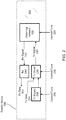
- Fig. 2 shows a functional block diagram of a Tx (transmitter) calibration system with tunable elements (i.e., Tx supply, Tx driver, matching network) in accordance with some embodiments of the invention.
- a reader device 200 is shown to include a Tx (transmitter) driver 230, a Tx supply 250, a Rx (receiver) 240, a matching network 220, and an antenna 222.
- a reader device can include a Tx (transmitter) unit (which can further include a Tx driver, Tx supply, etc.), a Rx (receiver) unit, a matching network, and an antenna.
- Tx (transmitter) unit which can further include a Tx driver, Tx supply, etc.
- Rx (receiver) unit a matching network, and an antenna.
- the Tx supply 250 provides a voltage to the Tx driver 230.
- Fig. 2 shows that the Tx driver 230 receives Tx data 234 as input, and then transmits Tx signal 232 as output.
- Fig. 2 also shows that the Rx 240 receives Rx data 242 as input, and then transmits Rx data 244 as output.
- Fig. 2 shows that the reader device 200 can control the Tx output with enhanced accuracy by using the Tx calibration data to tune the Tx supply 250, the Tx driver 230, and the matching network 220.
- Control/tune 258 is applied to Tx supply 250
- control/tune 238 is applied to Tx driver 230
- control/tune 228 is applied to matching network 220.
- tuning can be applied to all three functional blocks of device 200 (i.e., Tx supply 250, Tx driver 230, and matching network 220) to control the Tx output with enhanced accuracy.
- tuning can be applied to only one of three functional blocks of device 200 (i.e., Tx supply 250, Tx driver 230, and matching network 220) to control the Tx output with enhanced accuracy. In some embodiments, tuning can be applied to any combination of the three functional blocks of device 200 (i.e., Tx supply 250, Tx driver 230, and matching network 220) to control the Tx output with enhanced accuracy.
- Fig. 3 shows a functional block diagram of a Tx (transmitter) control unit that controls the Tx output by controlling/tuning the tunable elements (i.e., Tx supply, Tx driver, matching network) in accordance with some embodiments of the invention.
- Fig. 3 provides information on how a device can use calibration data to tune a Tx supply, a Tx driver, and a matching network.
- Fig. 3 shows that a desired target Tx output 362 and calibration data 370 are provided as inputs to Tx control unit 360. Then the Tx control unit 360 use these inputs to determine the tuning setting to send to the tunable elements (i.e., Tx supply, Tx driver, matching network).
- the tuning setting 358 is used to tune the Tx supply, while the tuning setting 338 is used to tune the Tx driver and the tuning setting 328 is used to tune the matching network.
- Fig. 4 provides details on how a device can use calibration data to tune a Tx supply, a Tx driver, and a matching network.
- Fig. 4 shows a functional block diagram of a reader device 400 with a Tx (transmitter) control unit 460 that controls the Tx output by controlling/tuning the tunable elements (i.e., Tx supply 450, Tx driver 430, matching network 420) in accordance with some embodiments of the invention.
- Tx transmitter
- a reader device 400 is shown to include a NFC controller device 402, a matching network 420, and an antenna 422.
- the NFC controller device 402 is shown to include a Tx (transmitter) driver 430, a Tx supply 450, a Rx (receiver) 440, a Tx controller unit 460, and Tx Calibration data 470.
- the Tx supply 450 provides an input to the Tx driver 430.
- the Tx driver 430 receives Tx data 434 as input, and then transmits Tx signal 432 as output to the matching network 420 and the antenna 422.
- Fig. 4 also shows that the Rx 440 receives Rx data 442 as input from the matching network 420 and the antenna 422, and in turn transmits Rx data 444 as output.
- Fig. 4 further shows that a desired target Tx output 462 and calibration data 470 are provided as inputs to Tx control unit 460. Then the Tx control unit 460 uses these inputs to determine the tuning setting to send to the tunable elements (i.e., Tx supply 450, Tx driver 430, matching network 420).
- the tuning setting 458 is used to tune the Tx supply 450, while the tuning setting 438 is used to tune the Tx driver 430 and the tuning setting 428 is used to tune the matching network 420.
- the Tx unit is comprised of: (i) a Tx supply, (ii) a Tx driver, (b) wherein the Tx control unit controls the Tx output with enhanced accuracy by using the Tx calibration data to tune one or more of the following: (i) the Tx supply, (ii) the Tx driver, (iii) the matching network.
- the device level and/or system level calibration of the Tx is achieved by controlling (and tuning) the Tx output to an accurate (target) level by utilizing one or more of the following tuning methods:
- the Tx unit is comprised of: (i) a Tx supply, (ii) a Tx driver, (b) wherein the Tx control unit controls the Tx output with enhanced accuracy by using the Tx calibration data to tune one or more of the following: (i) tuning a setting of the Tx supply, (ii) tuning a pulse modulation of the Tx driver, (iii) tuning an impedance of Tx driver transistors, (iv) tuning a biasing of the Tx driver, (v) tuning a number of drivers turned on, (vi) tuning the matching network.
- tuning a setting of the Tx driver supply can include changing the voltage setting of the Tx driver supply.
- pulse modulation can include PWM (pulse width modulation), PFM (pulse frequency modulation), PCM (pulse code modulation), PDM (pulse duration modulation), PAM (pulse amplitude modulation), PPM (pulse position modulation), etc.
- tuning a pulse modulation of the Tx driver can include changing a pulse modulation of the Tx driver.
- tuning a pulse modulation of the Tx driver can include changing a pulse width of the Tx driver.
- tuning an impedance of Tx driver transistors can include turn on and off Tx driver transistors.
- tuning a biasing of the Tx driver can include changing a voltage or a current to determine an operating point of a transistor circuit.
- the matching network can include resistive and reactive impedance.
- the matching network can include resistor, capacitor, and inductor.
- tuning the matching network can include changing an impedance setting of the matching network.
- tuning the matching network can include changing a variable capacitor of the matching network.
- the accuracy on the Tx output may be achieved in reference to a radiated Tx output power, an antenna voltage, or a voltage on any node in the matching network.
- control of the Tx output with enhanced accuracy is achieved with reference to one or more of the following: (a) a Tx power that is radiated from the device, (b) a Tx field strength that is radiated from the device, (c) a Tx output voltage that is fed to the matching network, (d) a voltage on any node in the matching network, (e) an antenna voltage, (f) a Rx input voltage.
- the Tx control unit can be a hardware and/or software unit that allows compensation to be applied on a desired (target) configuration to achieve correction for a highly accurate Tx power.
- the Tx control unit is one of the following: (a) a hardware functional block, (b) a software functional block, (c) a functional block comprising both hardware and software.
- the control of the Tx output power using calibration data is performed by a control mechanism to apply correction data to a desired configuration. In turn an offset to the (desired) control can be generated.
- the calibration data in need for the compensation and/or calibration as mentioned earlier need to be captured and stored. Different methods (as described below) are possible:
- full or partial configuration datasets mean that the configuration datasets can include a “full” table or a “partial” table.
- full or partial all the available desired output power settings can be listed, while, for a "partial” table, only some of the available desired output power settings are listed. This means that for a "partial” table, in some embodiments, interpolation can be used to determine the desired output power settings that are not available.
- the configuration datasets can include “absolute” values or “offset” values to apply.
- an “absolute” configuration dataset can provide absolute voltage values to apply
- an “offset” configuration dataset can provide offsets from a reference voltage value to apply.
- the Tx calibration data can be stored as one of the following: (a) a plurality of configuration parameter datasets to be applied to the device to achieve specific Tx output per available Tx output settings in a table, (b) a plurality of configuration parameter datasets to be applied to the device to achieve specific Tx output per available Tx output settings in a function.
- each configuration parameter dataset can be comprised of one or more of the following parameters: (a) Tx supply voltage, (b) pulse modulation of a Tx signal, (c) Tx impedance, (d) number of Tx drivers turned on, (e) impedance setting of the matching network.
- the Tx control unit can be implemented as one of the following: (a) a look-up table comprising the Tx calibration data, (b) a function comprising the Tx calibration data, (c) a combination of a look-up table and a function, the combination comprising the Tx calibration data.
- Fig. 5A shows an example look-up table 500A comprising Tx (transmitter) calibration data (i.e., parameter settings) that can be used to help control a target Tx output (e.g., a target Tx output power) with enhanced accuracy in accordance with some embodiments of the invention.
- Fig. 5A shows that a desired target Tx output power can be achieved by tuning these 3 parameters: a Tx supply HW (hardware) configuration, a PWM (pulse width modulation) %, and a Num Driver setting.
- Each Tx supply HW configuration setting corresponds to a Tx supply voltage, which can be found by using the linking table 500C from Fig. 5C .
- PWM pulsesing signals can be used with a duty cycle.
- the Num Driver setting can be representing how many Tx drivers in parallel are used. In the look-up table 500A, only 2 Tx drivers in parallel can be used, so Num Driver can be either 1 or 2, which represents 1 or 2 Tx driver(s) in parallel used.
- look-up table 500A take, for example, the first-row entry, where the desired target Tx output power is 0.3 mW.
- a Tx supply HW configuration setting of 0 a PWM of 10%, and a Num Driver setting of 1 should be used.
- the Tx supply HW configuration setting of 0 we go to the linking table 500C from Fig. 5C , where the Tx supply HW configuration setting of 0 corresponds to a Tx supply voltage of 1 volt.
- a Tx supply HW configuration setting of 8 a PWM of 50%, and a Num Driver setting of 1 should be used.
- the linking table 500C from Fig. 5C shows that the Tx supply HW configuration setting of 8 corresponds to a Tx supply voltage of 3 volt.
- Fig. 5B shows an example generic look-up table 500B comprising Tx (transmitter) calibration data (i.e., parameter settings) that can help control a target Tx output (e.g., a target Tx output power) with enhanced accuracy in accordance with some embodiments of the invention. Similar to Fig. 5A , Fig. 5B shows that a desired target Tx output power can be achieved by tuning these 3 parameters: a Tx supply HW (hardware) configuration, a PWM (pulse width modulation) %, and a Num Driver setting.
- Tx supply HW hardware
- PWM pulse width modulation
- Table 500B is a generic correction table.
- the settings are filled with a combination of settings for the Tx supply HW configuration (based on the Tx supply voltage), PWM %, and Num Driver to achieve the target Tx power. If done in production, any variance from IC (integrated circuit), matching network, antenna is covered in the settings. (Note: IC includes the tunable elements (i.e., Tx supply, Tx driver, etc.) of the device.)
- the input is the "Target Tx Power" as index into the LUT (look-up table), which provides the combination of settings to achieve the target Tx power with high accuracy.
- Fig. 5C shows an example linking table 500C, which links Tx supply hardware configuration setting with actual Tx supply voltage, in accordance with some embodiments of the invention.
- the use of linking table 500C has already been explained earlier in this disclosure.
- Fig. 6 shows a process flow diagram of a method for controlling a Tx (transmitter) output with enhanced accuracy by using Tx calibration data together with a Tx control unit in accordance with some embodiments of the invention.
- the method 600 begins at step 610, where the method generates, by a Tx (transmitter) unit of the device, a transmitted signal. Then, the method proceeds to step 620.
- step 620 the method controls, by a Tx (transmitter) control unit of the device, a Tx output using Tx calibration data, wherein the Tx calibration data is generated by testing at a device level and/or a system level, wherein the Tx calibration data enables the Tx control unit to control the Tx output with enhanced accuracy.
- step 630 the method transmits, by a matching network unit and an antenna of the device, the transmitted signal.
- an embodiment of a computer program product includes a computer useable storage medium to store a computer readable program that, when executed on a computer, causes the computer to perform operations, as described herein.
- the computer-useable or computer-readable medium can be an electronic, magnetic, optical, electromagnetic, infrared, or semiconductor system (or apparatus or device), or a propagation medium.
- Examples of a computer-readable medium include a semiconductor or solid-state memory, magnetic tape, a removable computer diskette, a random-access memory (RAM), a read-only memory (ROM), a rigid magnetic disc, and an optical disc.
- Examples of optical discs include a compact disc with read only memory (CD-ROM), a compact disc with read/write (CD-R/W), a digital video disc (DVD), and a Blu-ray disc.
- CD-ROM compact disc with read only memory
- CD-R/W compact disc with read/write
- DVD digital video disc
- Blu-ray disc Blu-ray disc.
Landscapes
- Engineering & Computer Science (AREA)
- Computer Networks & Wireless Communication (AREA)
- Signal Processing (AREA)
- Physics & Mathematics (AREA)
- Electromagnetism (AREA)
- Nonlinear Science (AREA)
- Transmitters (AREA)
- Power Engineering (AREA)
Abstract
Description
- The described embodiments relate generally to methods and devices that provide for communication via inductive coupling, and more particularly to methods and devices that provide for communication via inductive coupling with calibration data that enables the transmitters to control the transmitter output with enhanced accuracy.
- An NFC (Near Field Communication) enabled device is an example of a communications device that communicates via inductive coupling. NFC is a short-range wireless technology that allows communication between NFC enabled objects over a distance of less than 10cm. NFC is based on Radio Frequency Identification (RFID) standards. It is a technology that is designed to make an easier and more convenient world for us, enhancing the way we make transactions, exchange content and connect devices. The NFC tags one might see or create include contacts, URLs, map locations, text and much more.
- An NFC-enabled device can operate in various operating modes, such as reader/writer mode, card emulation mode, and peer-to-peer mode. For example, an NFC-enabled device in reader/writer mode can behave like a simple contactless card reader. It initiates communication by generating a magnetic field and then sending a command to the target. The target responds to the interrogator by retro-reflecting the incident wave. The specificity of NFC operating modes is that the target can be not only a tag or a contactless card, but also an NFC-enabled device that behaves like a contactless card (in card emulation mode). Usages of reader mode, for example, include information reading, when an NFC-enabled device is used to read data by waving it in front of electronic labels available on streets, bus stops, sightseeing monuments, ad banners, parcels, products or on business cards (vCard). But there are many other possible use cases.
- As another example, an NFC-enabled device in card emulation mode can allow the NFC-enabled device to act like smart cards, allowing users to perform transactions such as purchases, ticketing, and transit access control with just a touch. An NFC-enabled device in card emulation mode can be configured for either passive load modulation (PLM) or active load modulation (ALM). While, ALM is typically more complex than PLM, components for implementing ALM in a card-mode device (e.g., a mobile device) can be more compact and, because the card-mode device utilizes a power source to generate a magnetic field rather than just modulate a magnetic field created by a reader, an ALM card-mode device can have greater communications range than a PLM card-mode device.
- As a further example, peer-to-peer mode enables two NFC-enabled devices to communicate with each other to exchange information and share files, so that users of NFC-enabled devices can quickly share contact information and other files with a touch.
- In all these modes and other possible applications, where an NFC-enabled device is transmitting signal, it can be important to have an accurate transmitter output. As such, there are strong motivations to control the transmitter output with enhanced accuracy.
- This specification discloses methods and systems for controlling a NFC (near field communication) transmitter output with enhanced accuracy. This is achieved by first generating a set of Tx (transmitter) calibration data by testing/calibrating a NFC Tx (transmitter) at a device and/or system level. Then, in some embodiments, this set of Tx calibration data can be used by a Tx control unit to control the Tx outputs (such as Tx output power, Tx output voltage, Tx output current, etc.) with enhanced accuracy. In some embodiments, the Tx control unit controls the Tx output with enhanced accuracy by using the Tx calibration data to tune one or more of the following: (i) a Tx supply, (ii) a Tx driver, (iii) a matching network.
- The present invention provides for a device that communicates via inductive coupling, the device comprising: (a) a matching network; (b) an antenna; (c) a Tx (transmitter) unit, the Tx unit configured to generate a transmitted signal that is transmitted through the matching network and the antenna; (d) a Tx (transmitter) control unit, the Tx control unit configured to controlling a Tx output using Tx calibration data, (i) wherein the Tx calibration data is generated by testing at a device level and/or a system level, (ii) wherein the Tx calibration data enables the Tx control unit to control the Tx output with enhanced accuracy.
- In some embodiments, the Tx output is a Tx output power level.
- In some embodiments, the Tx output is a Tx output voltage level.
- In some embodiments, the Tx output is a Tx output current level.
- In some embodiments, the device further comprises: (e) a Rx (receiver) unit, the receiver unit configured to receive a signal from a counterpart device.
- In some embodiments, the device is an NFC-enabled device operating in one of the following modes: (a) reader/writer mode, (b) card mode with ALM (active load modulation), (c) peer-to-peer mode, wherein NFC stands for near field communication.
- In some embodiments, (a) the Tx unit is comprised of: (i) a Tx supply, (ii) a Tx driver, (b) wherein the Tx control unit controls the Tx output with enhanced accuracy by using the Tx calibration data to tune one or more of the following: (i) the Tx supply, (ii) the Tx driver, (iii) the matching network.
- In some embodiments, (a) the Tx unit is comprised of: (i) a Tx supply, (ii) a Tx driver, (b) wherein the Tx control unit controls the Tx output with enhanced accuracy by using the Tx calibration data to tune one or more of the following: (i) tuning a setting of the Tx supply, (ii) tuning a pulse modulation of the Tx driver, (iii) tuning an impedance of Tx driver transistors, (iv) tuning a biasing of the Tx driver, (v) tuning a number of drivers turned on, (vi) tuning the matching network.
- In some embodiments, tuning the matching network comprises: changing an impedance setting of the matching network.
- In some embodiments, control of the Tx output with enhanced accuracy is achieved with reference to one or more of the following: (a) a Tx power that is radiated from the device, (b) a Tx field strength that is radiated from the device, (c) a Tx output voltage that is fed to the matching network, (d) a voltage on any node in the matching network, (e) an antenna voltage, (f) a Rx input voltage.
- In some embodiments, the Tx control unit is one of the following: (a) a hardware functional block, (b) a software functional block, (c) a functional block comprising both hardware and software.
- In some embodiments, the Tx calibration data is stored as one of the following: (a) a plurality of configuration parameter datasets to be applied to the device to achieve specific Tx output per available Tx output settings in a table, (b) a plurality of configuration parameter datasets to be applied to the device to achieve specific Tx output per available Tx output settings in a function.
- In some embodiments, each configuration parameter dataset is comprised of one or more of the following parameters: (a) Tx supply voltage, (b) pulse modulation of a Tx signal, (c) Tx impedance, (d) number of Tx drivers turned on, (e) impedance setting of the matching network.
- In some embodiments, the Tx control unit is implemented as one of the following: (a) a look-up table comprising the Tx calibration data, (b) a function comprising the Tx calibration data, (c) a combination of a look-up table and a function, the combination comprising the Tx calibration data.
- The present invention also provides for a method for operating a device that communicates via inductive coupling, the method comprising: (a) generating, by a Tx (transmitter) unit of the device, a transmitted signal; (b) controlling, by a Tx (transmitter) control unit of the device, a Tx output using Tx calibration data, wherein the Tx calibration data is generated by testing at a device level and/or a system level, wherein the Tx calibration data enables the Tx control unit to control the Tx output with enhanced accuracy; (c) transmitting, by a matching network unit and an antenna of the device, the transmitted signal.
- In some embodiments, the Tx output is one of the following: (a) a Tx output power level, (b) a Tx output voltage level, (c) a Tx output current level.
- In some embodiments, the method further comprising: (d) receiving, by a Rx (receiver) unit of the device, a response from a counterpart device.
- In some embodiments, (a) the Tx unit is comprised of: (i) a Tx supply, (ii) a Tx driver, (b) wherein the step of controlling the Tx output using the Tx calibration data is comprised of the Tx control unit controlling the Tx output with enhanced accuracy by using the Tx calibration data to tune one or more of the following: (i) the Tx supply of the device, (ii) the Tx driver of the device, (iii) the matching network of the device.
- In some embodiments, (a) the Tx unit is comprised of: (i) a Tx supply, (ii) a Tx driver, (b) wherein the step of controlling the Tx output using the Tx calibration data is comprised of the Tx control unit controlling the Tx output with enhanced accuracy by using the Tx calibration data to tune one or more of the following: (i) tuning a setting of the Tx supply, (ii) tuning a pulse modulation of the Tx driver, (iii) tuning an impedance of Tx driver transistors, (iv) tuning a biasing of the Tx driver, (v) tuning a number of drivers turned on, (vi) tuning the matching network.
- The present invention provides for a computer program product comprising executable instructions encoded in a non-transitory computer readable medium which, when executed by a system, carry out or control the following method for operating a device that communicates via inductive coupling, the method comprising: (a) generating, by a Tx (transmitter) unit of the device, a transmitted signal; (b) controlling, by a Tx (transmitter) control unit of the device, a Tx output using Tx calibration data, wherein the Tx calibration data is generated by testing at a device level and/or a system level, wherein the Tx calibration data enables the Tx control unit to control the Tx output with enhanced accuracy; (c) transmitting, by a matching network unit and an antenna of the device, the transmitted signal.
- The above summary is not intended to represent every example embodiment within the scope of the current or future Claim sets. Additional example embodiments are discussed within the Figures and Detailed Description below. Other aspects and advantages of embodiments of the present invention will become apparent from the following detailed description taken in conjunction with the accompanying drawings.
-
-
Fig. 1 shows a functional block diagram of a reader device and a card (tag) device with relevant signal nodes highlighted in accordance with some embodiments of the invention. -
Fig. 2 shows a functional block diagram of a Tx (transmitter) calibration system with tunable elements (i.e., Tx supply, Tx driver, matching network) in accordance with some embodiments of the invention. -
Fig. 3 shows a functional block diagram of a Tx (transmitter) control unit that controls the Tx output by controlling/tuning the tunable elements (i.e., Tx supply, Tx driver, matching network) in accordance with some embodiments of the invention. -
Fig. 4 shows a functional block diagram of a reader device with a Tx (transmitter) control unit that controls the Tx output by controlling/tuning the tunable elements (i.e., Tx supply, Tx driver, matching network) in accordance with some embodiments of the invention. -
Fig. 5A shows an example look-up table comprising Tx (transmitter) calibration data (i.e., parameter settings) that that can be used to help control a target Tx output (e.g., a target Tx output power) with enhanced accuracy in accordance with some embodiments of the invention. -
Fig. 5B shows an example generic look-up table comprising Tx (transmitter) calibration data (i.e., parameter settings) that can help control a target Tx output (e.g., a target Tx output power) with enhanced accuracy in accordance with some embodiments of the invention. -
Fig. 5C shows an example linking table, which links Tx supply hardware configuration setting with actual Tx supply voltage, in accordance with some embodiments of the invention. -
Fig. 6 shows a process flow diagram of a method for controlling a Tx (transmitter) output with enhanced accuracy by using Tx calibration data together with a Tx control unit in accordance with some embodiments of the invention. - It will be readily understood that the components of the embodiments as generally described herein and illustrated in the appended figures could be arranged and designed in a wide variety of different configurations. Thus, the following more detailed description of various embodiments, as represented in the figures, is not intended to limit the scope of the present disclosure but is merely representative of various embodiments. While the various aspects of the embodiments are presented in drawings, the drawings are not necessarily drawn to scale unless specifically indicated.
- The present invention may be embodied in other specific forms without departing from its spirit or essential characteristics. The described embodiments are to be considered in all respects only as illustrative and not restrictive. The scope of the invention is, therefore, indicated by the appended claims rather than by this detailed description. All changes which come within the meaning and range of equivalency of the claims are to be embraced within their scope.
- Reference throughout this specification to features, advantages, or similar language does not imply that all the features and advantages that may be realized with the present invention should be or are in any single embodiment of the invention. Rather, language referring to the features and advantages is understood to mean that a specific feature, advantage, or characteristic described in connection with an embodiment is included in at least one embodiment of the present invention. Thus, discussions of the features and advantages, and similar language, throughout this specification may, but do not necessarily, refer to the same embodiment.
- Furthermore, the described features, advantages, and characteristics of the invention may be combined in any suitable manner in one or more embodiments. One skilled in the relevant art will recognize, in light of the description herein, that the invention can be practiced without one or more of the specific features or advantages of a particular embodiment. In other instances, additional features and advantages may be recognized in certain embodiments that may not be present in all embodiments of the invention.
- This specification discloses methods and systems for controlling a NFC (near field communication) transmitter output with enhanced accuracy. This is achieved by first doing a device and/or system level calibration of the Tx (transmitter) by testing at the device and/or system level. Then using the testing results to generate a set of Tx calibration data, which will be used by a Tx control unit to control the Tx outputs (such as Tx output power, Tx output voltage, Tx output current, etc.) with enhanced accuracy. In some embodiments, the Tx control unit controls the Tx output with enhanced accuracy by using the Tx calibration data to tune one or more of the following: (i) a Tx supply, (ii) a Tx driver, (iii) a matching network.
- An NFC-enabled device can use the NFC Tx (transmitter) when a NFC controller is in active mode (i.e., reader mode or card mode ALM). Therefore, this specification discloses methods and systems to calibrate the Tx (transmitter) output (e.g., output power, output voltage, output current) of a NFC (Near Field Communication) controller in active mode (i.e., reader mode or card mode ALM). One important point of this disclosure is that the calibration can be referenced to Tx output voltage (chip output), voltage at the antenna node (Vant), or even field strength of the radiated signal from the NFC-enabled device (with the latter two including the matching network), as well as other possible nodes so that the Tx output can be controlled with enhanced accuracy.
- In NFC-enabled systems, for both reader-mode and card-mode active load modulation (ALM), an accurate transmit power is important for controlling consistent performance over volume population, as well as when control of output power is needed (e.g., card-mode ALM). As the transmit power emitted at the antenna is driven by a voltage applied to the antenna, the accuracy requirement can also apply to the voltage at the antenna, which in turn is induced by the voltage at the Tx output, as well as the output (e.g., Tx output power, Tx output voltage, Tx output current, etc.) at other nodes.
- A second application of this disclosure is the loopback feature, where an NFC-enabled device's own Tx driver can be used as a signal generator to provide accurate reference test signals for (production) testing purposes, with the motivation to replace bulky, costly, slow (in control of signal output) external test equipment (such as signal generator) by an accurate feature of a DUT (device under test) itself. In other embodiments, where the Tx driver is used solely as a signal generator to provide accurate reference test signals for (production) testing purposes, it is possible to have a device with only a transmitter (i.e., no receiver is needed in the device, so the device only includes a transmitter).
-
Fig. 1 shows a functional block diagram of areader device 100 and a card (tag)device 110 with relevant signal nodes highlighted in accordance with some embodiments of the invention. InFig. 1 , thereader device 100 is shown to include a Tx (transmitter)driver 130, a Rx (receiver) 140, amatching network 120, and anantenna 122. In general, a reader device can include a Tx (transmitter) unit (which can further include a Tx driver, Tx supply, etc.), a Rx (receiver) unit, a matching network, and an antenna.Fig. 1 shows that theTx driver 130 receivesTx data 134 as input, and then transmits Tx signal 132 as output.Fig. 1 also shows that theRx 140 receivesRx data 142 as input, and then transmitsRx data 144 as output. -
Fig. 1 also shows a communicationcounterpart card device 110 together with anantenna 112. In some embodiments, thereader device 100 can initiate communication by generating a magnetic field and then sending a command to thetarget card device 110. The target card device can respond to the interrogator by retro-reflecting the incident wave together with load modulation. -
Fig. 1 is shown with areceiver 140, but, in some embodiments, where the Tx driver is used as a signal generator to provide accurate reference test signals for (production) testing purposes, it is possible to have a device with only a transmitter and a Tx (transmitter) control unit, since no receiver is needed in the device. The receiver is only needed, if the device needs to receive a signal. Therefore, in some embodiments, a device (that communicates via inductive coupling and is enhanced with Tx calibration that enables a Tx to control the Tx output with enhanced accuracy) can be comprising only a Tx (transmitter) and a Tx (transmitter) control unit, wherein the Tx calibration data is generated by testing at a device level and/or a system level, wherein the Tx calibration data enables the Tx control unit to control the Tx output with enhanced accuracy. In other words, this means that (a) a matching network, (b) an antenna, and (c) a receiver can all be optional to such a device, and, in some embodiments, a device will not include a matching network, an antenna, and a receiver. -
Fig. 1 shows a NFC-enabled system with a reader device 100 (i.e., in reader/writer mode) and a card (tag)device 110. However, in general,device 100 can be any NFC-enabled device that uses the transmitter. Therefore,device 100 can be (a) a NFC-enabled device in reader/writer mode, or (b) a NFC-enabled device in card mode with ALM (active load modulation), or (c) a NFC-enabled device in peer-to-peer mode. Consequently, in some embodiments,device 100 is a NFC-enabled device in reader/writer mode, while thecommunication counterpart device 110 is a NFC-enabled device in card mode (or simply a tag device). In some embodiments,device 100 is a NFC-enabled device in card mode with ALM (active load modulation), while thecommunication counterpart device 110 is a NFC-enabled device in reader/writer mode. In some embodiments,device 100 is a NFC-enabled device in peer-to-peer mode, while thecommunication counterpart device 110 is a second NFC-enabled device in peer-to-peer mode. -
Fig. 1 depicts a NFC-enabled system together with the relevant signals, voltages, power at the respective nodes.Fig. 1 showsTx output voltage 136,antenna voltage 126, radiated Tx power (shown as field strength H 182), and Rx input voltage 146 (which can be relevant in the loopback application). Please note that the Tx transmitted power (in the form of radiated Tx power) can be quantified as field-strength H with the unit A/m. - Some of the following Tx outputs are not shown in
Fig. 1 , but in some embodiments, control of the Tx output with enhanced accuracy is achieved with reference to one or more of the following: (a) a Tx power that is radiated from the device, (b) a Tx field strength that is radiated from the device, (c) a Tx output voltage that is fed to the matching network, (d) a voltage on any node in the matching network, (e) an antenna voltage, (f) a Rx input voltage. In general, the Tx output can be: (a) a Tx output power level, (b) a Tx output voltage level, (c) a Tx output current level. Furthermore, the Tx output can be measured from any possible nodes withindevice 100 that is after the output of the Tx and before the input of Rx. The possible node locations also include the radiated field betweendevice 100 andcommunication counterpart device 110. - For both use cases (i.e., (1) accurate Tx power and (2) loopback), the Tx outputs (such as Tx output power and Tx output voltage) are strongly impacted by any variation in the different components of a DUT (device under test), as well as, very importantly, any variation in the matching network. Therefore, a calibrated Tx driver can compensate for any variations in the different components of a DUT and the matching network.
- In some embodiments, the key point of this disclosure is to do a device level and/or a system level calibration of the Tx (transmitter) by testing at the device level and/or the system level. Then using the testing results to generate a set of Tx calibration data, which will be used by a Tx control unit to control a Tx output (such as a Tx output power, a Tx output voltage, a Tx output current, etc.). In some embodiments, a device level calibration can include testing and calibrating at the IC (integrated circuit) die level up to testing and calibrating at the device level (where the device can be a
NFC controller device 402 or areader device 400 as shown inFig. 4 , or the device can be areader device 400 as shown inFig. 4 minus the receiver, matching network, and antenna). In some embodiments, a system level calibration can include testing and calibrating at the device level up to testing and calibrating at the system level (where the system can be "areader device 100" or "areader device 100 plus acard device 110" as shown inFig. 1 ). -
Fig. 2 shows a functional block diagram of a Tx (transmitter) calibration system with tunable elements (i.e., Tx supply, Tx driver, matching network) in accordance with some embodiments of the invention. InFig. 2 , areader device 200 is shown to include a Tx (transmitter)driver 230, aTx supply 250, a Rx (receiver) 240, amatching network 220, and anantenna 222. In general, a reader device can include a Tx (transmitter) unit (which can further include a Tx driver, Tx supply, etc.), a Rx (receiver) unit, a matching network, and an antenna. InFig. 2 , theTx supply 250 provides a voltage to theTx driver 230.Fig. 2 shows that theTx driver 230 receivesTx data 234 as input, and then transmits Tx signal 232 as output.Fig. 2 also shows that theRx 240 receivesRx data 242 as input, and then transmitsRx data 244 as output. -
Fig. 2 shows that thereader device 200 can control the Tx output with enhanced accuracy by using the Tx calibration data to tune theTx supply 250, theTx driver 230, and thematching network 220. Control/tune 258 is applied toTx supply 250, while control/tune 238 is applied toTx driver 230 and control/tune 228 is applied to matchingnetwork 220. In some embodiments, tuning can be applied to all three functional blocks of device 200 (i.e.,Tx supply 250,Tx driver 230, and matching network 220) to control the Tx output with enhanced accuracy. In some embodiments, tuning can be applied to only one of three functional blocks of device 200 (i.e.,Tx supply 250,Tx driver 230, and matching network 220) to control the Tx output with enhanced accuracy. In some embodiments, tuning can be applied to any combination of the three functional blocks of device 200 (i.e.,Tx supply 250,Tx driver 230, and matching network 220) to control the Tx output with enhanced accuracy. -
Fig. 3 shows a functional block diagram of a Tx (transmitter) control unit that controls the Tx output by controlling/tuning the tunable elements (i.e., Tx supply, Tx driver, matching network) in accordance with some embodiments of the invention.Fig. 3 provides information on how a device can use calibration data to tune a Tx supply, a Tx driver, and a matching network.Fig. 3 shows that a desiredtarget Tx output 362 andcalibration data 370 are provided as inputs toTx control unit 360. Then theTx control unit 360 use these inputs to determine the tuning setting to send to the tunable elements (i.e., Tx supply, Tx driver, matching network). The tuning setting 358 is used to tune the Tx supply, while the tuning setting 338 is used to tune the Tx driver and the tuning setting 328 is used to tune the matching network. -
Fig. 4 provides details on how a device can use calibration data to tune a Tx supply, a Tx driver, and a matching network.Fig. 4 shows a functional block diagram of areader device 400 with a Tx (transmitter)control unit 460 that controls the Tx output by controlling/tuning the tunable elements (i.e.,Tx supply 450,Tx driver 430, matching network 420) in accordance with some embodiments of the invention. - In
Fig. 4 , areader device 400 is shown to include aNFC controller device 402, amatching network 420, and anantenna 422. TheNFC controller device 402 is shown to include a Tx (transmitter)driver 430, aTx supply 450, a Rx (receiver) 440, aTx controller unit 460, and Tx Calibration data 470. - In
Fig. 4 , theTx supply 450 provides an input to theTx driver 430.Fig. 4 shows that theTx driver 430 receivesTx data 434 as input, and then transmits Tx signal 432 as output to thematching network 420 and theantenna 422.Fig. 4 also shows that theRx 440 receivesRx data 442 as input from thematching network 420 and theantenna 422, and in turn transmitsRx data 444 as output. -
Fig. 4 further shows that a desiredtarget Tx output 462 and calibration data 470 are provided as inputs toTx control unit 460. Then theTx control unit 460 uses these inputs to determine the tuning setting to send to the tunable elements (i.e.,Tx supply 450,Tx driver 430, matching network 420). The tuning setting 458 is used to tune theTx supply 450, while the tuning setting 438 is used to tune theTx driver 430 and the tuning setting 428 is used to tune thematching network 420. - In some embodiments, (a) the Tx unit is comprised of: (i) a Tx supply, (ii) a Tx driver, (b) wherein the Tx control unit controls the Tx output with enhanced accuracy by using the Tx calibration data to tune one or more of the following: (i) the Tx supply, (ii) the Tx driver, (iii) the matching network.
- In some embodiments, the device level and/or system level calibration of the Tx is achieved by controlling (and tuning) the Tx output to an accurate (target) level by utilizing one or more of the following tuning methods:
- (a). changing the setting of the Tx driver supply (e.g., changing the voltage setting of the Tx driver supply),
- (b). tuning the pulse modulation of the Tx driver (e.g., changing the pulse width),
- (c). tuning the impedance (Tx Rdson) of the Tx driver transistors,
- (d). tuning the driver biasing,
- (e). tuning the matching network,
- (f). etc.
- In some embodiments, (a) the Tx unit is comprised of: (i) a Tx supply, (ii) a Tx driver, (b) wherein the Tx control unit controls the Tx output with enhanced accuracy by using the Tx calibration data to tune one or more of the following: (i) tuning a setting of the Tx supply, (ii) tuning a pulse modulation of the Tx driver, (iii) tuning an impedance of Tx driver transistors, (iv) tuning a biasing of the Tx driver, (v) tuning a number of drivers turned on, (vi) tuning the matching network.
- In some embodiments, tuning a setting of the Tx driver supply can include changing the voltage setting of the Tx driver supply.
- In some embodiments, pulse modulation can include PWM (pulse width modulation), PFM (pulse frequency modulation), PCM (pulse code modulation), PDM (pulse duration modulation), PAM (pulse amplitude modulation), PPM (pulse position modulation), etc. In some embodiments, tuning a pulse modulation of the Tx driver can include changing a pulse modulation of the Tx driver. In some embodiments, tuning a pulse modulation of the Tx driver can include changing a pulse width of the Tx driver.
- In some embodiments, tuning an impedance of Tx driver transistors can include turn on and off Tx driver transistors.
- In some embodiments, tuning a biasing of the Tx driver can include changing a voltage or a current to determine an operating point of a transistor circuit. In some embodiments, the matching network can include resistive and reactive impedance. In some embodiments, the matching network can include resistor, capacitor, and inductor. In some embodiments, tuning the matching network can include changing an impedance setting of the matching network. In some embodiments, tuning the matching network can include changing a variable capacitor of the matching network.
- In turn, the accuracy on the Tx output (such as Tx output power) may be achieved in reference to a radiated Tx output power, an antenna voltage, or a voltage on any node in the matching network. In some embodiments, control of the Tx output with enhanced accuracy is achieved with reference to one or more of the following: (a) a Tx power that is radiated from the device, (b) a Tx field strength that is radiated from the device, (c) a Tx output voltage that is fed to the matching network, (d) a voltage on any node in the matching network, (e) an antenna voltage, (f) a Rx input voltage.
- The Tx control unit can be a hardware and/or software unit that allows compensation to be applied on a desired (target) configuration to achieve correction for a highly accurate Tx power. In some embodiments, the Tx control unit is one of the following: (a) a hardware functional block, (b) a software functional block, (c) a functional block comprising both hardware and software.
- The control of the Tx output power using calibration data is performed by a control mechanism to apply correction data to a desired configuration. In turn an offset to the (desired) control can be generated.
The calibration data in need for the compensation and/or calibration as mentioned earlier need to be captured and stored. Different methods (as described below) are possible: - (a). Calibration data stored as configuration datasets to be applied to achieve specific target output power per available desired output power settings in a table (e.g., a look-up table).
- (b). Calibration data stored as configuration datasets to be applied to achieve specific target output power per available desired output power settings in a function.
- (c). Calibration data stored as "full or partial" and "absolute or offset" configuration datasets to be applied to achieve specific target output power per available desired output power settings in a table (e.g., a look-up table).
- (d). Calibration data stored as "full or partial" and "absolute or offset" configuration datasets to be applied to achieve specific target output power per available desired output power settings in a function.
- (e). Other methods are also possible.
- For the above, "full or partial" configuration datasets mean that the configuration datasets can include a "full" table or a "partial" table. For a "full" table, all the available desired output power settings can be listed, while, for a "partial" table, only some of the available desired output power settings are listed. This means that for a "partial" table, in some embodiments, interpolation can be used to determine the desired output power settings that are not available.
- For the above, "absolute or offset" configuration datasets mean that the configuration datasets can include "absolute" values or "offset" values to apply. For example, an "absolute" configuration dataset can provide absolute voltage values to apply, while an "offset" configuration dataset can provide offsets from a reference voltage value to apply. In some embodiments, the Tx calibration data can be stored as one of the following: (a) a plurality of configuration parameter datasets to be applied to the device to achieve specific Tx output per available Tx output settings in a table, (b) a plurality of configuration parameter datasets to be applied to the device to achieve specific Tx output per available Tx output settings in a function.
- In some embodiments, each configuration parameter dataset can be comprised of one or more of the following parameters: (a) Tx supply voltage, (b) pulse modulation of a Tx signal, (c) Tx impedance, (d) number of Tx drivers turned on, (e) impedance setting of the matching network.
- In some embodiments, the Tx control unit can be implemented as one of the following: (a) a look-up table comprising the Tx calibration data, (b) a function comprising the Tx calibration data, (c) a combination of a look-up table and a function, the combination comprising the Tx calibration data.
-
Fig. 5A shows an example look-up table 500A comprising Tx (transmitter) calibration data (i.e., parameter settings) that can be used to help control a target Tx output (e.g., a target Tx output power) with enhanced accuracy in accordance with some embodiments of the invention.Fig. 5A shows that a desired target Tx output power can be achieved by tuning these 3 parameters: a Tx supply HW (hardware) configuration, a PWM (pulse width modulation) %, and a Num Driver setting. Each Tx supply HW configuration setting corresponds to a Tx supply voltage, which can be found by using the linking table 500C fromFig. 5C . In PWM, pulsing signals can be used with a duty cycle. Here the PWM % can be representing a scaling to the maximum power possible with PWM tuning, so that a higher PWM % represents a higher Tx power. (Note: PWM % = 100 can represent the maximum power possible with PWM tuning.) The Num Driver setting can be representing how many Tx drivers in parallel are used. In the look-up table 500A, only 2 Tx drivers in parallel can be used, so Num Driver can be either 1 or 2, which represents 1 or 2 Tx driver(s) in parallel used. - To understand look-up table 500A, take, for example, the first-row entry, where the desired target Tx output power is 0.3 mW. Here, to achieve a desired target Tx output power of 0.3 mW, then a Tx supply HW configuration setting of 0, a PWM of 10%, and a Num Driver setting of 1 should be used. To understand the Tx supply HW configuration setting of 0, we go to the linking table 500C from
Fig. 5C , where the Tx supply HW configuration setting of 0 corresponds to a Tx supply voltage of 1 volt. As another example, look at the 13th row entry of 56.3 mW. Here, to achieve a desired target Tx output power of 56.3 mW, then a Tx supply HW configuration setting of 8, a PWM of 50%, and a Num Driver setting of 1 should be used. Here, the linking table 500C fromFig. 5C shows that the Tx supply HW configuration setting of 8 corresponds to a Tx supply voltage of 3 volt. -
Fig. 5B shows an example generic look-up table 500B comprising Tx (transmitter) calibration data (i.e., parameter settings) that can help control a target Tx output (e.g., a target Tx output power) with enhanced accuracy in accordance with some embodiments of the invention. Similar toFig. 5A ,Fig. 5B shows that a desired target Tx output power can be achieved by tuning these 3 parameters: a Tx supply HW (hardware) configuration, a PWM (pulse width modulation) %, and a Num Driver setting. - Table 500B is a generic correction table. During calibration, the settings are filled with a combination of settings for the Tx supply HW configuration (based on the Tx supply voltage), PWM %, and Num Driver to achieve the target Tx power. If done in production, any variance from IC (integrated circuit), matching network, antenna is covered in the settings. (Note: IC includes the tunable elements (i.e., Tx supply, Tx driver, etc.) of the device.) During the use-case of "accurate Tx power", the input is the "Target Tx Power" as index into the LUT (look-up table), which provides the combination of settings to achieve the target Tx power with high accuracy.
-
Fig. 5C shows an example linking table 500C, which links Tx supply hardware configuration setting with actual Tx supply voltage, in accordance with some embodiments of the invention. The use of linking table 500C has already been explained earlier in this disclosure. -
Fig. 6 shows a process flow diagram of a method for controlling a Tx (transmitter) output with enhanced accuracy by using Tx calibration data together with a Tx control unit in accordance with some embodiments of the invention. As shown inFig. 6 , themethod 600 begins atstep 610, where the method generates, by a Tx (transmitter) unit of the device, a transmitted signal. Then, the method proceeds to step 620. Instep 620, the method controls, by a Tx (transmitter) control unit of the device, a Tx output using Tx calibration data, wherein the Tx calibration data is generated by testing at a device level and/or a system level, wherein the Tx calibration data enables the Tx control unit to control the Tx output with enhanced accuracy. Finally, atstep 630, the method transmits, by a matching network unit and an antenna of the device, the transmitted signal. - In this specification, example embodiments have been presented in terms of a selected set of details. However, a person of ordinary skill in the art would understand that many other example embodiments may be practiced which include a different selected set of these details. It is intended that the following claims cover all possible example embodiments.
- Although the operations of the method(s) herein are shown and described in a particular order, the order of the operations of each method may be altered so that certain operations may be performed in an inverse order or so that certain operations may be performed, at least in part, concurrently with other operations. In another embodiment, instructions or sub-operations of distinct operations may be implemented in an intermittent and/or alternating manner.
- It should also be noted that at least some of the operations for the methods may be implemented using software instructions stored on a computer useable storage medium for execution by a computer. As an example, an embodiment of a computer program product includes a computer useable storage medium to store a computer readable program that, when executed on a computer, causes the computer to perform operations, as described herein.
- The computer-useable or computer-readable medium can be an electronic, magnetic, optical, electromagnetic, infrared, or semiconductor system (or apparatus or device), or a propagation medium. Examples of a computer-readable medium include a semiconductor or solid-state memory, magnetic tape, a removable computer diskette, a random-access memory (RAM), a read-only memory (ROM), a rigid magnetic disc, and an optical disc. Examples of optical discs include a compact disc with read only memory (CD-ROM), a compact disc with read/write (CD-R/W), a digital video disc (DVD), and a Blu-ray disc. The various aspects, embodiments, implementations or features of the described embodiments can be used separately or in any combination. Various aspects of the described embodiments can be implemented by software, hardware or a combination of hardware and software.
- The foregoing description, for purposes of explanation, used specific nomenclature to provide a thorough understanding of the described embodiments. However, it will be apparent to one skilled in the art that the specific details are not required in order to practice the described embodiments. Thus, the foregoing descriptions of specific embodiments are presented for purposes of illustration and description. They are not intended to be exhaustive or to limit the described embodiments to the precise forms disclosed. It will be apparent to one of ordinary skill in the art that many modifications and variations are possible in view of the above teachings.
Claims (15)
- A device that communicates via inductive coupling, the device comprising:- a matching network;- an antenna;- a Tx (transmitter) unit, the Tx unit configured to generate a transmitted signal that is transmitted through the matching network and the antenna;- a Tx (transmitter) control unit, the Tx control unit configured to controlling a Tx output using Tx calibration data,wherein the Tx calibration data is generated by testing at a device level and/or a system level,wherein the Tx calibration data enables the Tx control unit to control the Tx output with enhanced accuracy.
- The device of claim 1, wherein the Tx output is a Tx output power level, a Tx output voltage level, or a Tx output current level.
- The device of claim 1 or 2, further comprising:- a Rx (receiver) unit, the receiver unit configured to receive a signal from a counterpart device.
- The device of claim 3,
wherein the device is an NFC-enabled device operating in one of the following modes:- reader/writer mode,- card mode with ALM (active load modulation),- peer-to-peer mode,wherein NFC stands for near field communication. - The device of any preceding claim,
wherein the Tx unit is comprised of:- a Tx supply,- a Tx driver,wherein the Tx control unit controls the Tx output with enhanced accuracy by using the Tx calibration data to tune one or more of the following:- the Tx supply,- the Tx driver,- the matching network. - The device of any preceding claim,
wherein the Tx unit is comprised of:- a Tx supply,- a Tx driver,wherein the Tx control unit controls the Tx output with enhanced accuracy by using the Tx calibration data to tune one or more of the following:- tuning a setting of the Tx supply,- tuning a pulse modulation of the Tx driver,- tuning an impedance of Tx driver transistors,- tuning a biasing of the Tx driver,- tuning a number of drivers turned on,- tuning the matching network. - The device of claim 6, wherein tuning the matching network comprises:
changing an impedance setting of the matching network. - The device of any preceding claim, wherein control of the Tx output with enhanced accuracy is achieved with reference to one or more of the following:- a Tx power that is radiated from the device,- a Tx field strength that is radiated from the device,- a Tx output voltage that is fed to the matching network,- a voltage on any node in the matching network,- an antenna voltage,- a Rx input voltage.
- The device of any preceding claim, wherein the Tx control unit is one of the following:- a hardware functional block,- a software functional block,- a functional block comprising both hardware and software.
- The device of any preceding claim, wherein the Tx calibration data is stored as one of the following:- a plurality of configuration parameter datasets to be applied to the device to achieve specific Tx output per available Tx output settings in a table,- a plurality of configuration parameter datasets to be applied to the device to achieve specific Tx output per available Tx output settings in a function.
- The device of claim 10, wherein each configuration parameter dataset is comprised of one or more of the following parameters:- Tx supply voltage,- pulse modulation of a Tx signal,- Tx impedance,- number of Tx drivers turned on,- impedance setting of the matching network.
- The device of any preceding claim, wherein the Tx control unit is implemented as one of the following:- a look-up table comprising the Tx calibration data,- a function comprising the Tx calibration data,- a combination of a look-up table and a function, the combination comprising the Tx calibration data.
- A method for operating a device that communicates via inductive coupling, the method comprising:- generating, by a Tx (transmitter) unit of the device, a transmitted signal;- controlling, by a Tx (transmitter) control unit of the device, a Tx output using Tx calibration data,wherein the Tx calibration data is generated by testing at a device level and/or a system level,wherein the Tx calibration data enables the Tx control unit to control the Tx output with enhanced accuracy;- transmitting, by a matching network unit and an antenna of the device, the transmitted signal.
- The method of claim 13, wherein the Tx output is one of the following:- a Tx output power level,- a Tx output voltage level,- a Tx output current level.
- A computer program product comprising executable instructions encoded in a non-transitory computer readable medium which, when executed by a system, carry out or control the method of claim 13 or 14.
Applications Claiming Priority (1)
| Application Number | Priority Date | Filing Date | Title |
|---|---|---|---|
| US16/049,436 US10644756B2 (en) | 2018-07-30 | 2018-07-30 | Transmitter calibration for NFC (near field communication) device |
Publications (2)
| Publication Number | Publication Date |
|---|---|
| EP3605854A1 true EP3605854A1 (en) | 2020-02-05 |
| EP3605854B1 EP3605854B1 (en) | 2021-10-13 |
Family
ID=65991572
Family Applications (1)
| Application Number | Title | Priority Date | Filing Date |
|---|---|---|---|
| EP19165116.5A Active EP3605854B1 (en) | 2018-07-30 | 2019-03-26 | Transmitter calibration for nfc (near field communication) device |
Country Status (3)
| Country | Link |
|---|---|
| US (1) | US10644756B2 (en) |
| EP (1) | EP3605854B1 (en) |
| CN (1) | CN110784271B (en) |
Families Citing this family (2)
| Publication number | Priority date | Publication date | Assignee | Title |
|---|---|---|---|---|
| US10893492B2 (en) * | 2019-01-19 | 2021-01-12 | Maxim Integrated Products, Inc. | Near field communication reader with dynamic power control |
| KR102594118B1 (en) * | 2019-02-22 | 2023-10-25 | 삼성전자주식회사 | A wireless communication device for detecting card |
Citations (3)
| Publication number | Priority date | Publication date | Assignee | Title |
|---|---|---|---|---|
| US20160134382A1 (en) * | 2014-11-07 | 2016-05-12 | Qualcomm Incorporated | Systems and methods for self-calibration for wireless communication |
| US20180034510A1 (en) * | 2016-08-01 | 2018-02-01 | Nxp B.V. | Method and system to measure the phase offset based on the frequency response in a nfc system |
| EP3319239A1 (en) * | 2016-11-08 | 2018-05-09 | Nxp B.V. | Method and system for automatic power control (apc) in a communications device that communicates via inductive coupling |
Family Cites Families (24)
| Publication number | Priority date | Publication date | Assignee | Title |
|---|---|---|---|---|
| US6556814B1 (en) * | 1999-07-22 | 2003-04-29 | Motorola, Inc. | Memory-based amplifier load adjust system |
| KR100500921B1 (en) * | 2003-08-25 | 2005-07-14 | 주식회사 하이닉스반도체 | Semiconductor memory device with ability to mediate impedance of data output-driver |
| US8152304B2 (en) * | 2006-08-30 | 2012-04-10 | International Business Machines Corporation | Stereographic imaging system using open loop magnetomechanically resonant polarizing filter actuator |
| US8373403B1 (en) * | 2008-08-08 | 2013-02-12 | Power-One, Inc. | Circuit for controlling synchronous rectifiers during start-up into pre-biased output voltage |
| US8131232B2 (en) * | 2009-10-09 | 2012-03-06 | Texas Instruments Incorporated | Method and apparatus for antenna tuning |
| US8294514B2 (en) * | 2010-09-24 | 2012-10-23 | St-Ericsson Sa | Calibrate output matching for correct output power |
| US8451031B2 (en) * | 2010-11-11 | 2013-05-28 | Advanced Micro Devices, Inc. | Adjustable finite impulse response transmitter |
| US9564676B2 (en) * | 2011-06-30 | 2017-02-07 | Google Technology Holdings LLC | System and methods for adaptive antenna optimization |
| US20130226496A1 (en) * | 2012-02-29 | 2013-08-29 | Qualcomm Incorporated | Precise calibration of electronic components |
| US9467008B2 (en) * | 2012-07-28 | 2016-10-11 | WIPQTUS Inc. | Input power appraisal based wireless power system |
| US8638838B1 (en) * | 2012-08-27 | 2014-01-28 | Teradici Corporation | Differential serial interface for supporting a plurality of differential serial interface standards |
| US20140080409A1 (en) * | 2012-09-17 | 2014-03-20 | Qualcomm Incorporated | Static tuning of wireless transmitters |
| US9450646B2 (en) * | 2013-03-15 | 2016-09-20 | Qualcomm Incorporated | Direct power transmission load modulation in near field communication devices |
| US20140353300A1 (en) * | 2013-06-03 | 2014-12-04 | John A. Swiatek | Automated local thermal management system |
| US9049664B2 (en) * | 2013-06-24 | 2015-06-02 | Mediatek Inc. | Wireless communications circuit for improving current consumption and RF performance |
| WO2015015720A1 (en) * | 2013-07-31 | 2015-02-05 | パナソニック株式会社 | Power transmission apparatus and wireless power transmission system |
| US9960791B2 (en) * | 2013-12-12 | 2018-05-01 | Ethertronics, Inc. | RF integrated circuit with tunable component and memory |
| US20150249354A1 (en) * | 2014-02-28 | 2015-09-03 | Infineon Technologies Austria Ag | Communication using load modulation |
| KR102229022B1 (en) * | 2014-03-18 | 2021-03-17 | 삼성전자주식회사 | Device of detecting card having magnetic field monitor and System including the same |
| US9876515B2 (en) * | 2014-06-05 | 2018-01-23 | Nokia Technologies Oy | Adaptive transmitter efficiency optimization |
| US9438224B2 (en) * | 2014-06-25 | 2016-09-06 | Freescale Semiconductor, Inc. | Devices with signal characteristic dependent control circuitry and methods of operation therefor |
| KR20160050651A (en) * | 2014-10-30 | 2016-05-11 | 한국전자통신연구원 | System for managing livestock house and method therof |
| US9756578B2 (en) | 2015-04-10 | 2017-09-05 | Qualcomm Incorporated | Systems and methods for transmit power control |
| KR102027558B1 (en) * | 2015-07-30 | 2019-10-01 | 엘에스산전 주식회사 | Power loss measuring system for measuring power loss at harmonic filter included in high voltage direct current(hvdc) ststem and method for measuring power loss thereof |
-
2018
- 2018-07-30 US US16/049,436 patent/US10644756B2/en active Active
-
2019
- 2019-03-26 EP EP19165116.5A patent/EP3605854B1/en active Active
- 2019-07-30 CN CN201910699675.2A patent/CN110784271B/en active Active
Patent Citations (3)
| Publication number | Priority date | Publication date | Assignee | Title |
|---|---|---|---|---|
| US20160134382A1 (en) * | 2014-11-07 | 2016-05-12 | Qualcomm Incorporated | Systems and methods for self-calibration for wireless communication |
| US20180034510A1 (en) * | 2016-08-01 | 2018-02-01 | Nxp B.V. | Method and system to measure the phase offset based on the frequency response in a nfc system |
| EP3319239A1 (en) * | 2016-11-08 | 2018-05-09 | Nxp B.V. | Method and system for automatic power control (apc) in a communications device that communicates via inductive coupling |
Also Published As
| Publication number | Publication date |
|---|---|
| EP3605854B1 (en) | 2021-10-13 |
| US20200036412A1 (en) | 2020-01-30 |
| US10644756B2 (en) | 2020-05-05 |
| CN110784271A (en) | 2020-02-11 |
| CN110784271B (en) | 2023-06-16 |
Similar Documents
| Publication | Publication Date | Title |
|---|---|---|
| US10749616B2 (en) | Method for a phase calibration in a frontend circuit of a near field communication device | |
| CN102856666B (en) | Control the antenna performance of near field communication means | |
| EP2582063B1 (en) | Shaped load modulation in a near field communications (NFC) device | |
| KR101610835B1 (en) | Nfc transceiver | |
| EP3461018B1 (en) | Method and system for operating a communications device that communicates via inductive coupling | |
| EP3605854B1 (en) | Transmitter calibration for nfc (near field communication) device | |
| EP2713524A2 (en) | Remote antenna driver for reducing unwanted electromagnetic emissions and/or distortion within a near field communication (NFC) capable device | |
| US10574303B1 (en) | System and method to test and calibrate card-detection using active tag emulation | |
| EP2816737B1 (en) | Secure near field communication | |
| US12289140B2 (en) | Devices and methods for near-field communication detection | |
| KR102023624B1 (en) | Radio frequency transmission circuit and apparatuses including the same | |
| JP7751471B2 (en) | Waveform shaping to prevent overshoot and undershoot | |
| US20250088833A1 (en) | RF communication device for adaptive detection of further RF communication devices | |
| EP3751462B1 (en) | Transponder and corresponding operating method | |
| US10461811B2 (en) | Method and system for automatic power control (APC) in a communications device that communicates via inductive coupling | |
| JP2008108043A (en) | Non-contact data carrier read / write device, antenna output circuit and antenna circuit. | |
| HK1193246A (en) | A near field communication (nfc) device and an antenna module thereof | |
| HK1182543B (en) | Near field communications (nfc) device and method of communication in the nfc device |
Legal Events
| Date | Code | Title | Description |
|---|---|---|---|
| PUAI | Public reference made under article 153(3) epc to a published international application that has entered the european phase |
Free format text: ORIGINAL CODE: 0009012 |
|
| STAA | Information on the status of an ep patent application or granted ep patent |
Free format text: STATUS: THE APPLICATION HAS BEEN PUBLISHED |
|
| AK | Designated contracting states |
Kind code of ref document: A1 Designated state(s): AL AT BE BG CH CY CZ DE DK EE ES FI FR GB GR HR HU IE IS IT LI LT LU LV MC MK MT NL NO PL PT RO RS SE SI SK SM TR |
|
| AX | Request for extension of the european patent |
Extension state: BA ME |
|
| STAA | Information on the status of an ep patent application or granted ep patent |
Free format text: STATUS: REQUEST FOR EXAMINATION WAS MADE |
|
| 17P | Request for examination filed |
Effective date: 20200805 |
|
| RBV | Designated contracting states (corrected) |
Designated state(s): AL AT BE BG CH CY CZ DE DK EE ES FI FR GB GR HR HU IE IS IT LI LT LU LV MC MK MT NL NO PL PT RO RS SE SI SK SM TR |
|
| STAA | Information on the status of an ep patent application or granted ep patent |
Free format text: STATUS: EXAMINATION IS IN PROGRESS |
|
| 17Q | First examination report despatched |
Effective date: 20201123 |
|
| GRAP | Despatch of communication of intention to grant a patent |
Free format text: ORIGINAL CODE: EPIDOSNIGR1 |
|
| STAA | Information on the status of an ep patent application or granted ep patent |
Free format text: STATUS: GRANT OF PATENT IS INTENDED |
|
| INTG | Intention to grant announced |
Effective date: 20210705 |
|
| GRAS | Grant fee paid |
Free format text: ORIGINAL CODE: EPIDOSNIGR3 |
|
| GRAA | (expected) grant |
Free format text: ORIGINAL CODE: 0009210 |
|
| STAA | Information on the status of an ep patent application or granted ep patent |
Free format text: STATUS: THE PATENT HAS BEEN GRANTED |
|
| AK | Designated contracting states |
Kind code of ref document: B1 Designated state(s): AL AT BE BG CH CY CZ DE DK EE ES FI FR GB GR HR HU IE IS IT LI LT LU LV MC MK MT NL NO PL PT RO RS SE SI SK SM TR |
|
| REG | Reference to a national code |
Ref country code: GB Ref legal event code: FG4D |
|
| REG | Reference to a national code |
Ref country code: CH Ref legal event code: EP |
|
| REG | Reference to a national code |
Ref country code: DE Ref legal event code: R096 Ref document number: 602019008253 Country of ref document: DE |
|
| REG | Reference to a national code |
Ref country code: IE Ref legal event code: FG4D |
|
| REG | Reference to a national code |
Ref country code: AT Ref legal event code: REF Ref document number: 1438922 Country of ref document: AT Kind code of ref document: T Effective date: 20211115 |
|
| REG | Reference to a national code |
Ref country code: LT Ref legal event code: MG9D |
|
| REG | Reference to a national code |
Ref country code: NL Ref legal event code: MP Effective date: 20211013 |
|
| REG | Reference to a national code |
Ref country code: AT Ref legal event code: MK05 Ref document number: 1438922 Country of ref document: AT Kind code of ref document: T Effective date: 20211013 |
|
| PG25 | Lapsed in a contracting state [announced via postgrant information from national office to epo] |
Ref country code: RS Free format text: LAPSE BECAUSE OF FAILURE TO SUBMIT A TRANSLATION OF THE DESCRIPTION OR TO PAY THE FEE WITHIN THE PRESCRIBED TIME-LIMIT Effective date: 20211013 Ref country code: LT Free format text: LAPSE BECAUSE OF FAILURE TO SUBMIT A TRANSLATION OF THE DESCRIPTION OR TO PAY THE FEE WITHIN THE PRESCRIBED TIME-LIMIT Effective date: 20211013 Ref country code: FI Free format text: LAPSE BECAUSE OF FAILURE TO SUBMIT A TRANSLATION OF THE DESCRIPTION OR TO PAY THE FEE WITHIN THE PRESCRIBED TIME-LIMIT Effective date: 20211013 Ref country code: BG Free format text: LAPSE BECAUSE OF FAILURE TO SUBMIT A TRANSLATION OF THE DESCRIPTION OR TO PAY THE FEE WITHIN THE PRESCRIBED TIME-LIMIT Effective date: 20220113 Ref country code: AT Free format text: LAPSE BECAUSE OF FAILURE TO SUBMIT A TRANSLATION OF THE DESCRIPTION OR TO PAY THE FEE WITHIN THE PRESCRIBED TIME-LIMIT Effective date: 20211013 |
|
| PG25 | Lapsed in a contracting state [announced via postgrant information from national office to epo] |
Ref country code: IS Free format text: LAPSE BECAUSE OF FAILURE TO SUBMIT A TRANSLATION OF THE DESCRIPTION OR TO PAY THE FEE WITHIN THE PRESCRIBED TIME-LIMIT Effective date: 20220213 Ref country code: SE Free format text: LAPSE BECAUSE OF FAILURE TO SUBMIT A TRANSLATION OF THE DESCRIPTION OR TO PAY THE FEE WITHIN THE PRESCRIBED TIME-LIMIT Effective date: 20211013 Ref country code: PT Free format text: LAPSE BECAUSE OF FAILURE TO SUBMIT A TRANSLATION OF THE DESCRIPTION OR TO PAY THE FEE WITHIN THE PRESCRIBED TIME-LIMIT Effective date: 20220214 Ref country code: PL Free format text: LAPSE BECAUSE OF FAILURE TO SUBMIT A TRANSLATION OF THE DESCRIPTION OR TO PAY THE FEE WITHIN THE PRESCRIBED TIME-LIMIT Effective date: 20211013 Ref country code: NO Free format text: LAPSE BECAUSE OF FAILURE TO SUBMIT A TRANSLATION OF THE DESCRIPTION OR TO PAY THE FEE WITHIN THE PRESCRIBED TIME-LIMIT Effective date: 20220113 Ref country code: NL Free format text: LAPSE BECAUSE OF FAILURE TO SUBMIT A TRANSLATION OF THE DESCRIPTION OR TO PAY THE FEE WITHIN THE PRESCRIBED TIME-LIMIT Effective date: 20211013 Ref country code: LV Free format text: LAPSE BECAUSE OF FAILURE TO SUBMIT A TRANSLATION OF THE DESCRIPTION OR TO PAY THE FEE WITHIN THE PRESCRIBED TIME-LIMIT Effective date: 20211013 Ref country code: HR Free format text: LAPSE BECAUSE OF FAILURE TO SUBMIT A TRANSLATION OF THE DESCRIPTION OR TO PAY THE FEE WITHIN THE PRESCRIBED TIME-LIMIT Effective date: 20211013 Ref country code: GR Free format text: LAPSE BECAUSE OF FAILURE TO SUBMIT A TRANSLATION OF THE DESCRIPTION OR TO PAY THE FEE WITHIN THE PRESCRIBED TIME-LIMIT Effective date: 20220114 Ref country code: ES Free format text: LAPSE BECAUSE OF FAILURE TO SUBMIT A TRANSLATION OF THE DESCRIPTION OR TO PAY THE FEE WITHIN THE PRESCRIBED TIME-LIMIT Effective date: 20211013 |
|
| REG | Reference to a national code |
Ref country code: DE Ref legal event code: R097 Ref document number: 602019008253 Country of ref document: DE |
|
| PG25 | Lapsed in a contracting state [announced via postgrant information from national office to epo] |
Ref country code: SM Free format text: LAPSE BECAUSE OF FAILURE TO SUBMIT A TRANSLATION OF THE DESCRIPTION OR TO PAY THE FEE WITHIN THE PRESCRIBED TIME-LIMIT Effective date: 20211013 Ref country code: SK Free format text: LAPSE BECAUSE OF FAILURE TO SUBMIT A TRANSLATION OF THE DESCRIPTION OR TO PAY THE FEE WITHIN THE PRESCRIBED TIME-LIMIT Effective date: 20211013 Ref country code: RO Free format text: LAPSE BECAUSE OF FAILURE TO SUBMIT A TRANSLATION OF THE DESCRIPTION OR TO PAY THE FEE WITHIN THE PRESCRIBED TIME-LIMIT Effective date: 20211013 Ref country code: EE Free format text: LAPSE BECAUSE OF FAILURE TO SUBMIT A TRANSLATION OF THE DESCRIPTION OR TO PAY THE FEE WITHIN THE PRESCRIBED TIME-LIMIT Effective date: 20211013 Ref country code: DK Free format text: LAPSE BECAUSE OF FAILURE TO SUBMIT A TRANSLATION OF THE DESCRIPTION OR TO PAY THE FEE WITHIN THE PRESCRIBED TIME-LIMIT Effective date: 20211013 Ref country code: CZ Free format text: LAPSE BECAUSE OF FAILURE TO SUBMIT A TRANSLATION OF THE DESCRIPTION OR TO PAY THE FEE WITHIN THE PRESCRIBED TIME-LIMIT Effective date: 20211013 |
|
| PLBE | No opposition filed within time limit |
Free format text: ORIGINAL CODE: 0009261 |
|
| STAA | Information on the status of an ep patent application or granted ep patent |
Free format text: STATUS: NO OPPOSITION FILED WITHIN TIME LIMIT |
|
| 26N | No opposition filed |
Effective date: 20220714 |
|
| PG25 | Lapsed in a contracting state [announced via postgrant information from national office to epo] |
Ref country code: MC Free format text: LAPSE BECAUSE OF FAILURE TO SUBMIT A TRANSLATION OF THE DESCRIPTION OR TO PAY THE FEE WITHIN THE PRESCRIBED TIME-LIMIT Effective date: 20211013 Ref country code: AL Free format text: LAPSE BECAUSE OF FAILURE TO SUBMIT A TRANSLATION OF THE DESCRIPTION OR TO PAY THE FEE WITHIN THE PRESCRIBED TIME-LIMIT Effective date: 20211013 |
|
| REG | Reference to a national code |
Ref country code: CH Ref legal event code: PL |
|
| PG25 | Lapsed in a contracting state [announced via postgrant information from national office to epo] |
Ref country code: SI Free format text: LAPSE BECAUSE OF FAILURE TO SUBMIT A TRANSLATION OF THE DESCRIPTION OR TO PAY THE FEE WITHIN THE PRESCRIBED TIME-LIMIT Effective date: 20211013 |
|
| REG | Reference to a national code |
Ref country code: BE Ref legal event code: MM Effective date: 20220331 |
|
| PG25 | Lapsed in a contracting state [announced via postgrant information from national office to epo] |
Ref country code: LU Free format text: LAPSE BECAUSE OF NON-PAYMENT OF DUE FEES Effective date: 20220326 Ref country code: LI Free format text: LAPSE BECAUSE OF NON-PAYMENT OF DUE FEES Effective date: 20220331 Ref country code: IE Free format text: LAPSE BECAUSE OF NON-PAYMENT OF DUE FEES Effective date: 20220326 Ref country code: FR Free format text: LAPSE BECAUSE OF NON-PAYMENT OF DUE FEES Effective date: 20220331 Ref country code: CH Free format text: LAPSE BECAUSE OF NON-PAYMENT OF DUE FEES Effective date: 20220331 |
|
| PG25 | Lapsed in a contracting state [announced via postgrant information from national office to epo] |
Ref country code: BE Free format text: LAPSE BECAUSE OF NON-PAYMENT OF DUE FEES Effective date: 20220331 |
|
| PG25 | Lapsed in a contracting state [announced via postgrant information from national office to epo] |
Ref country code: IT Free format text: LAPSE BECAUSE OF FAILURE TO SUBMIT A TRANSLATION OF THE DESCRIPTION OR TO PAY THE FEE WITHIN THE PRESCRIBED TIME-LIMIT Effective date: 20211013 |
|
| P01 | Opt-out of the competence of the unified patent court (upc) registered |
Effective date: 20230725 |
|
| GBPC | Gb: european patent ceased through non-payment of renewal fee |
Effective date: 20230326 |
|
| PG25 | Lapsed in a contracting state [announced via postgrant information from national office to epo] |
Ref country code: GB Free format text: LAPSE BECAUSE OF NON-PAYMENT OF DUE FEES Effective date: 20230326 |
|
| PG25 | Lapsed in a contracting state [announced via postgrant information from national office to epo] |
Ref country code: GB Free format text: LAPSE BECAUSE OF NON-PAYMENT OF DUE FEES Effective date: 20230326 |
|
| PG25 | Lapsed in a contracting state [announced via postgrant information from national office to epo] |
Ref country code: MK Free format text: LAPSE BECAUSE OF FAILURE TO SUBMIT A TRANSLATION OF THE DESCRIPTION OR TO PAY THE FEE WITHIN THE PRESCRIBED TIME-LIMIT Effective date: 20211013 Ref country code: CY Free format text: LAPSE BECAUSE OF FAILURE TO SUBMIT A TRANSLATION OF THE DESCRIPTION OR TO PAY THE FEE WITHIN THE PRESCRIBED TIME-LIMIT Effective date: 20211013 |
|
| PG25 | Lapsed in a contracting state [announced via postgrant information from national office to epo] |
Ref country code: HU Free format text: LAPSE BECAUSE OF FAILURE TO SUBMIT A TRANSLATION OF THE DESCRIPTION OR TO PAY THE FEE WITHIN THE PRESCRIBED TIME-LIMIT; INVALID AB INITIO Effective date: 20190326 |
|
| PG25 | Lapsed in a contracting state [announced via postgrant information from national office to epo] |
Ref country code: TR Free format text: LAPSE BECAUSE OF FAILURE TO SUBMIT A TRANSLATION OF THE DESCRIPTION OR TO PAY THE FEE WITHIN THE PRESCRIBED TIME-LIMIT Effective date: 20211013 |
|
| PG25 | Lapsed in a contracting state [announced via postgrant information from national office to epo] |
Ref country code: MT Free format text: LAPSE BECAUSE OF FAILURE TO SUBMIT A TRANSLATION OF THE DESCRIPTION OR TO PAY THE FEE WITHIN THE PRESCRIBED TIME-LIMIT Effective date: 20211013 |
|
| PGFP | Annual fee paid to national office [announced via postgrant information from national office to epo] |
Ref country code: DE Payment date: 20260219 Year of fee payment: 8 |