EP3605811A1 - Switching control device - Google Patents
Switching control device Download PDFInfo
- Publication number
- EP3605811A1 EP3605811A1 EP17902287.6A EP17902287A EP3605811A1 EP 3605811 A1 EP3605811 A1 EP 3605811A1 EP 17902287 A EP17902287 A EP 17902287A EP 3605811 A1 EP3605811 A1 EP 3605811A1
- Authority
- EP
- European Patent Office
- Prior art keywords
- terminal
- circuit
- fet
- drive circuit
- reverse bias
- Prior art date
- Legal status (The legal status is an assumption and is not a legal conclusion. Google has not performed a legal analysis and makes no representation as to the accuracy of the status listed.)
- Granted
Links
Images


Classifications
-
- H—ELECTRICITY
- H03—ELECTRONIC CIRCUITRY
- H03K—PULSE TECHNIQUE
- H03K17/00—Electronic switching or gating, i.e. not by contact-making and –breaking
- H03K17/04—Modifications for accelerating switching
- H03K17/041—Modifications for accelerating switching without feedback from the output circuit to the control circuit
- H03K17/0412—Modifications for accelerating switching without feedback from the output circuit to the control circuit by measures taken in the control circuit
- H03K17/04123—Modifications for accelerating switching without feedback from the output circuit to the control circuit by measures taken in the control circuit in field-effect transistor switches
-
- H—ELECTRICITY
- H02—GENERATION; CONVERSION OR DISTRIBUTION OF ELECTRIC POWER
- H02M—APPARATUS FOR CONVERSION BETWEEN AC AND AC, BETWEEN AC AND DC, OR BETWEEN DC AND DC, AND FOR USE WITH MAINS OR SIMILAR POWER SUPPLY SYSTEMS; CONVERSION OF DC OR AC INPUT POWER INTO SURGE OUTPUT POWER; CONTROL OR REGULATION THEREOF
- H02M3/00—Conversion of DC power input into DC power output
- H02M3/22—Conversion of DC power input into DC power output with intermediate conversion into AC
- H02M3/24—Conversion of DC power input into DC power output with intermediate conversion into AC by static converters
- H02M3/28—Conversion of DC power input into DC power output with intermediate conversion into AC by static converters using discharge tubes with control electrode or semiconductor devices with control electrode to produce the intermediate AC
- H02M3/325—Conversion of DC power input into DC power output with intermediate conversion into AC by static converters using discharge tubes with control electrode or semiconductor devices with control electrode to produce the intermediate AC using devices of a triode or a transistor type requiring continuous application of a control signal
- H02M3/335—Conversion of DC power input into DC power output with intermediate conversion into AC by static converters using discharge tubes with control electrode or semiconductor devices with control electrode to produce the intermediate AC using devices of a triode or a transistor type requiring continuous application of a control signal using semiconductor devices only
- H02M3/33569—Conversion of DC power input into DC power output with intermediate conversion into AC by static converters using discharge tubes with control electrode or semiconductor devices with control electrode to produce the intermediate AC using devices of a triode or a transistor type requiring continuous application of a control signal using semiconductor devices only having several active switching elements
- H02M3/33576—Conversion of DC power input into DC power output with intermediate conversion into AC by static converters using discharge tubes with control electrode or semiconductor devices with control electrode to produce the intermediate AC using devices of a triode or a transistor type requiring continuous application of a control signal using semiconductor devices only having several active switching elements having at least one active switching element at the secondary side of an isolation transformer
- H02M3/33592—Conversion of DC power input into DC power output with intermediate conversion into AC by static converters using discharge tubes with control electrode or semiconductor devices with control electrode to produce the intermediate AC using devices of a triode or a transistor type requiring continuous application of a control signal using semiconductor devices only having several active switching elements having at least one active switching element at the secondary side of an isolation transformer having a synchronous rectifier circuit or a synchronous freewheeling circuit at the secondary side of an isolation transformer
-
- H—ELECTRICITY
- H03—ELECTRONIC CIRCUITRY
- H03K—PULSE TECHNIQUE
- H03K17/00—Electronic switching or gating, i.e. not by contact-making and –breaking
- H03K17/51—Electronic switching or gating, i.e. not by contact-making and –breaking characterised by the components used
- H03K17/56—Electronic switching or gating, i.e. not by contact-making and –breaking characterised by the components used by the use, as active elements, of semiconductor devices
- H03K17/687—Electronic switching or gating, i.e. not by contact-making and –breaking characterised by the components used by the use, as active elements, of semiconductor devices the devices being field-effect transistors
- H03K17/689—Electronic switching or gating, i.e. not by contact-making and –breaking characterised by the components used by the use, as active elements, of semiconductor devices the devices being field-effect transistors with galvanic isolation between the control circuit and the output circuit
- H03K17/691—Electronic switching or gating, i.e. not by contact-making and –breaking characterised by the components used by the use, as active elements, of semiconductor devices the devices being field-effect transistors with galvanic isolation between the control circuit and the output circuit using transformer coupling
-
- H—ELECTRICITY
- H03—ELECTRONIC CIRCUITRY
- H03K—PULSE TECHNIQUE
- H03K17/00—Electronic switching or gating, i.e. not by contact-making and –breaking
- H03K17/51—Electronic switching or gating, i.e. not by contact-making and –breaking characterised by the components used
- H03K17/78—Electronic switching or gating, i.e. not by contact-making and –breaking characterised by the components used using opto-electronic devices, i.e. light-emitting and photoelectric devices electrically- or optically-coupled
- H03K17/785—Electronic switching or gating, i.e. not by contact-making and –breaking characterised by the components used using opto-electronic devices, i.e. light-emitting and photoelectric devices electrically- or optically-coupled controlling field-effect transistor switches
-
- H—ELECTRICITY
- H03—ELECTRONIC CIRCUITRY
- H03K—PULSE TECHNIQUE
- H03K17/00—Electronic switching or gating, i.e. not by contact-making and –breaking
- H03K17/04—Modifications for accelerating switching
- H03K17/041—Modifications for accelerating switching without feedback from the output circuit to the control circuit
- H03K17/0416—Modifications for accelerating switching without feedback from the output circuit to the control circuit by measures taken in the output circuit
- H03K17/04163—Modifications for accelerating switching without feedback from the output circuit to the control circuit by measures taken in the output circuit in field-effect transistor switches
-
- H—ELECTRICITY
- H03—ELECTRONIC CIRCUITRY
- H03K—PULSE TECHNIQUE
- H03K2217/00—Indexing scheme related to electronic switching or gating, i.e. not by contact-making or -breaking covered by H03K17/00
- H03K2217/0081—Power supply means, e.g. to the switch driver
Definitions
- the present invention relates to a switching control device.
- a DC/DC converter includes a switching circuit that converts DC power to AC power, a transformer that transforms the AC power converted by the switching circuit, and a rectifier circuit that rectifies the AC power transformed by the transformer to DC power, and a switching control device that controls the switching circuit.
- the switching control device performs a conversion into a predetermined AC power, for example, by performing an ON/OFF control of a switching element of the switching circuit.
- Patent Literature 1 Japanese Patent Application Laid-open No. 2008-67475
- the conventional switching control device may include a reverse bias circuit that applies a reverse bias voltage to the switching element of the switching circuit to quickly turn off the switching element, but the number of components constituting the reverse bias circuit tends to increase, and there is room for further improvement in this respect.
- an object of the present invention is to provide a switching control device capable of suppressing an increase in the number of components constituting the reverse bias circuit.
- a switching control device includes a drive circuit that is connected to a control terminal of a switching element connected to a DC power supply to be transformed and controlled to be turned on or off, and applies a voltage to the control terminal to turn on the switching element, the switching element including an input terminal to which a current is input, an output terminal that outputs the current input from the input terminal, and the control terminal that controls the current flowing from the input terminal to the output terminal; and a reverse bias circuit that includes a capacitor connected to the output terminal, and a coil having one end connected between the drive circuit and the control terminal and the other end connected between the capacitor and the output terminal.
- a switching control device includes a reverse bias circuit including a capacitor connected to an output terminal of a switching element, and a coil having one end connected between a drive circuit and a control terminal of a switching element and the other end connected between the capacitor and an output terminal of the switching element.
- the switching control device can apply a reverse bias voltage to the output terminal of the switching element by the reverse bias circuit.
- the reverse bias circuit can be configured by the coil and the capacitor, it is possible to suppress an increase in the number of components constituting the reverse bias circuit.
- the DC/DC converter 1 is, for example, an isolated switching power supply.
- the DC/DC converter 1 transforms a voltage of DC power supplied from a DC power supply (battery) of a vehicle, for example.
- the DC/DC converter 1 includes a primary circuit 10, a secondary circuit (not illustrated), and a switching control device 20 that controls the primary circuit 10.
- the primary circuit 10 includes a switching circuit 11 and a primary winding 12 connected to the switching circuit 11.
- the switching circuit 11 is a circuit which is connected to the DC power supply VPP to be transformed and converts the DC power supplied from the DC power supply VPP into AC power.
- the DC power supply VPP is a relatively high voltage, for example, a voltage of about 100 V to 200 V.
- the switching circuit 11 is, for example, a full bridge circuit configured by four switching elements. In FIG. 1 , two switching elements Q1 and Q2 are illustrated in a switching circuit 11, and the remaining two switching elements are not illustrated.
- Each of the switching elements Q1 and Q2 is, for example, an N-channel type Metal-Oxide-Semiconductor Field-Effect Transistor (MOSFET), and hereinafter, also simply referred to as FETs Q1 and Q2.
- a drain terminal d1 as an input terminal of the FET Q1 is connected to the power supply VPP.
- MOSFET Metal-Oxide-Semiconductor Field-Effect Transistor
- a secondary circuit (not illustrated) includes a secondary wiring installed opposite to a primary winding 12, a rectifying circuit connected to the secondary wiring and rectifying the AC power output from the secondary wiring into DC power, and a smoothing circuit connected to the rectifying circuit and smoothing DC current output from the rectifying circuit.
- the DC/DC converter 1 converts DC power supplied from the DC power supply VPP into AC power by a switching circuit 11, transforms the converted AC power by the primary winding 12 and the secondary winding, rectifies the transformed AC power by the rectifying circuit, smooths the DC power rectified by the rectifying circuit by a smoothing circuit, and supplies the same to a load part.
- a switching control device 20 is a device that controls four switching elements (FETs Q1, Q2, and the like) of a switching circuit 11.
- the switching control device 20 includes a drive circuit 21 and a reverse bias circuit 22 for each switching element.
- the switching control device 20 includes a drive circuit 21A that controls the FET Q1 of the switching circuit 11 and a reverse bias circuit 22A, and includes a drive circuit 21B that controls the FET Q2 of the switching circuit 11 and a reverse bias circuit 22B. Since the four drive circuits 21 have the same configuration, the drive circuits 21A and 21B for respectively driving the FETs Q1 and Q2 of the switching circuit 11 are illustrated, and the drive circuits 21 for controlling the remaining two switching elements of the switching circuit 11 are not illustrated.
- reverse bias circuits 22A and 22B for respectively applying reverse bias voltages to the FETs Q1 and Q2 of the switching circuit 11 are illustrated, and the reverse bias circuits 22 for controlling the remaining two switching elements of the switching circuit 11 are not illustrated. Since a configuration and an operation of the drive circuit 21A for driving the FET Q1 are the same as those of the drive circuit 21B for driving the FET Q2 in the switching control device 20, the drive circuit 21A will be described in detail, and the description of the drive circuit 21B will be omitted in the following description.
- the reverse bias circuit 22A applying the reverse bias voltage to the FET Q1 are the same as those of the reverse bias circuit 22B applying the reverse bias voltage to the FET Q2 in the switching control device 20, the reverse bias circuit 22A will be described in detail, and the description of the reverse bias circuit 22B will be omitted in the following description.
- the drive circuit 21A is a circuit that controls the FET Q1 of the switching circuit 11 to be on or off.
- the drive circuit 21A includes a primary drive circuit 211 and a secondary drive circuit 212.
- the primary drive circuit 211 includes a power supply VCC of a low voltage (for example, about 12 V), an npn bipolar transistor Q3 (hereinafter, also simply referred to as a transistor Q3), and a pnp bipolar transistor Q4 (hereinafter, simply referred to as a transistor Q4), a primary winding PT1, a resistor R1, and capacitors C1 and C2.
- the transistor Q3 has a collector terminal connected to the power supply VCC, and an emitter terminal connected to an emitter terminal of the transistor Q4.
- a connection point of the transistor Q3 and the transistor Q4 is connected to one end of the primary winding PT1 via a resistor R1.
- the other end of the primary winding PT1 is connected to one end of the capacitor C1.
- the other end of the capacitor C1 and the collector terminal of the transistor Q4 are connected to the ground.
- a base terminal of the transistor Q3 and a base terminal of the transistor Q4 are connected to a pulse output circuit (not illustrated).
- the capacitor C2 is connected to the power supply VCC and stabilizes a power supplied from the power supply VCC.
- the primary drive circuit 211 performs an ON/OFF control of the transistors Q3 and Q4 based on a pulse signal output from a pulse output circuit, and outputs AC power (pulse signal) to the primary winding PT1.
- the secondary drive circuit 212 includes a secondary winding PT2, a power supply VCC2 of a low voltage (for example, about 12 V), a diode D1, an N-channel MOSFET Q5 (hereinafter, also simply referred to as an FET Q5), a P-channel MOSFET Q6 (hereinafter, also simply referred to as an FET Q6), and a capacitor C3.
- the primary winding PT1 and the secondary winding PT2 isolate the primary drive circuit 211 and the secondary drive circuit 212, and constitute a pulse transformer for generating a pulse signal.
- a gate terminal of the FET Q5 and a gate terminal of the FET Q6 are connected to one end of the secondary winding PT2.
- the FET Q5 has a drain terminal connected to the power supply VCC2 via the diode D1 and a source terminal connected to the drain terminal of the FET Q6.
- a connection point of the FET Q5 and the FET Q6 is connected to a gate terminal g1 as a control terminal of the FET Q1 via a resistor R2.
- a source terminal of the FET Q6 is connected between the other end of the secondary winding PT2 and a capacitor C4.
- the secondary drive circuit 212 performs an ON/OFF control of the FETs Q5 and Q6 based on an AC power (pulse signal) output via the secondary winding PT2 to apply a voltage to the gate terminal g1 of the FET Q1.
- the reverse bias circuit 22A includes a capacitor C4 and a coil L1.
- the capacitor C4 has one end connected to a source terminal s1 as an output terminal of the FET Q1, and the other end connected to the other end of the secondary winding PT2.
- the coil L1 has one end connected between a source terminal of the FET Q5 and the gate terminal g1 of the FET Q1 and the other end connected between the capacitor C4 and the source terminal s1 of the FET Q1.
- the reverse bias circuit 22A energy is stored in the coil L1 when the FET Q5 is turned on and the FET Q6 is turned off. Further, when the FET Q5 is turned off and the FET Q6 is turned on, the reverse bias circuit 22A discharges the energy stored in the coil L1, and charges the capacitor C4 with the discharged energy. The reverse bias circuit 22A applies a voltage to the source terminal s1 of the FET Q1 by the energy charged in the capacitor C4 to turns the FET Q1 into a reverse bias state.
- the coil L1 preferably has an inductance value by which a continuous mode can be realized in which a reverse bias voltage is continuously output when the FET Q1 is turned off. Therefore, in order to realize the continuous mode, the coil L1 preferably has an inductance value that satisfies the following equation (1).
- the coil L1 satisfies the following equation (1): L > VCC 2 ⁇ Ton ⁇ Toff / 2 ⁇ IG ⁇ Ton + Toff
- the coil L1 When the coil L1 does not satisfy the inductance value of the equation (1), it turns into an intermittent mode where the reverse bias voltage is intermittently output, but it is possible to apply the reverse bias voltage to the FET Q1 even in the intermittent mode.
- the reverse bias circuit 22A turns the FET Q1 into a reverse bias state by the energy charged in the capacitor C4.
- the switching control device 20 includes the drive circuit 21 and the reverse bias circuit 22.
- the drive circuit 21A which is an FET Q1 connected to a DC power supply VPP to be transformed and controlled to be turned on or off, is connected to the gate terminal g1 of the FET Q1 having the drain terminal d1 to which a current is input, a source terminal s1 for outputting current input from the drain terminal d1, and the gate terminal g1 for controlling the current flowing from the drain terminal d1 to the source terminal s1, and applies the voltage to the gate terminal g1 to turn on the FET Q1.
- the reverse bias circuit 22A includes the capacitor C4 connected to the source terminal s1 of the FET Q1, and the coil L1 having one end connected between the drive circuit 21A and the gate terminal g1 and the other end connected between the capacitor C4 and the source terminal s1.
- the switching control device 20 can store energy in the coil L1. Then, when the FET Q1 is turned off by the drive circuit 21A in the switching control device 20, the energy stored in the coil L1 of the reverse bias circuit 22A may be discharged, the capacitor C4 may be charged with the discharged energy, and a reverse bias voltage can be applied to the source terminal s1 of the FET Q1 by the energy charged in the capacitor C4. As a result, the switching control device 20 can eliminate at once carriers existing between the drain terminal d1 and the source terminal s1 of the FET Q1, quickly turning off the FET Q1.
- the reverse bias circuit 22A can be configured with the coil L1 and the capacitor C4, the reverse bias circuit 22A can be configured with a relatively small number of components, and it is possible to suppress an increase in the number of the components constituting the reverse bias circuit 22A. As a result, the switching control device 20 can suppress the circuit from being enlarged and suppress a manufacturing cost.
- the switching control device 20 can realize a continuous mode in which the reverse bias voltage is continuously output when the FET Q1 is off, and apply the reverse bias voltage to the FET Q1 stably.
- the embodiment is not limited thereto.
- the drive circuit 21A may use a photocoupler 21a instead of the pulse transformer.
- the photocoupler 21a includes a light emitting element 21b and a light receiving element 21c.
- the light emitting element 21b is, for example, a light emitting diode, and has an anode terminal connected between a transistor Q3 and a transistor Q4 via a resistor R1 and a cathode terminal connected to the ground.
- the light receiving element 21c is, for example, a phototransistor, and has one end connected to a gate terminal of an FET Q5 and a gate terminal of an FET Q6 and the other end connected to the capacitor C4.
- an optical signal is output from the light emitting element 21b when the current flows through the light emitting element 21b, and the optical signal output from the light emitting element 21b is received by the light receiving element 21c.
- the drive circuit 21C converts the received light signal into an electric signal (pulse signal) and outputs it to the gate terminal of the FET Q5 and the gate terminal of the FET Q6 to perform an ON/OF control of the FETs Q5 and Q6.
- the drive circuit 21C may be configured to have the photocoupler 21a.
- the drive circuit 21 may be configured with an Integrated Circuit (IC) circuit 21d.
- a drive circuit 21D includes, as the IC circuit 21d on the primary side, an input terminal IN connected to the pulse output circuit, a power supply terminal VCC1 connected to a power supply VCC, and a ground terminal GND1 connected to the ground.
- the drive circuit 21D includes, as an IC circuit 21d on the secondary side, an output terminal OUT connected to the gate terminal g1 of the FET Q1, a power supply terminal VCC3 connected to the power supply VCC2, and a ground terminal GND2 connected to the ground.
- the input terminal IN and the output terminal OUT are isolated.
- the drive circuit 21D When an ON signal is input from the pulse output circuit to the input terminal IN, the drive circuit 21D outputs an electrical signal that is applied to the gate terminal g1 of the FET Q1 from the output terminal OUT.
- the drive circuit 21D may be configured to have the IC circuit 21d.
- each of the FETs Q1, Q2 and the like of the switching circuit 11 is the MOSFET
- Each of the FETs Q1 and Q2, and the like may be, for example, a transistor such as a bipolar transistor.
- the switching circuit 11 has been described as a full bridge system, it is not limited thereto, and may be a half bridge system, a push-pull system, or the like.
- the DC/DC converter 1 is the isolated DC/DC converter
- it may be a non-isolated DC/DC converter.
Landscapes
- Engineering & Computer Science (AREA)
- Power Engineering (AREA)
- Dc-Dc Converters (AREA)
- Power Conversion In General (AREA)
- Electronic Switches (AREA)
Abstract
Description
- The present invention relates to a switching control device.
- Conventionally, for example, a DC/DC converter includes a switching circuit that converts DC power to AC power, a transformer that transforms the AC power converted by the switching circuit, and a rectifier circuit that rectifies the AC power transformed by the transformer to DC power, and a switching control device that controls the switching circuit. The switching control device performs a conversion into a predetermined AC power, for example, by performing an ON/OFF control of a switching element of the switching circuit.
- Patent Literature 1: Japanese Patent Application Laid-open No.
2008-67475 - By the way, the conventional switching control device may include a reverse bias circuit that applies a reverse bias voltage to the switching element of the switching circuit to quickly turn off the switching element, but the number of components constituting the reverse bias circuit tends to increase, and there is room for further improvement in this respect.
- Therefore, the present invention has been made in view of the above problem, and an object of the present invention is to provide a switching control device capable of suppressing an increase in the number of components constituting the reverse bias circuit.
- In order to solve the above mentioned problem and achieve the object, a switching control device according to the present invention includes a drive circuit that is connected to a control terminal of a switching element connected to a DC power supply to be transformed and controlled to be turned on or off, and applies a voltage to the control terminal to turn on the switching element, the switching element including an input terminal to which a current is input, an output terminal that outputs the current input from the input terminal, and the control terminal that controls the current flowing from the input terminal to the output terminal; and a reverse bias circuit that includes a capacitor connected to the output terminal, and a coil having one end connected between the drive circuit and the control terminal and the other end connected between the capacitor and the output terminal.
- Further, in the switching control device, when an inductance value of the coil is L, a voltage applied to the drive circuit is VCC2, an ON period per cycle during which the voltage is applied to the control terminal by the drive circuit is Ton, an OFF period per cycle during which the voltage is not applied to the control terminal by the drive circuit is Toff, and a current value of the control terminal is IG, it is preferable that the following equation (1) is satisfied:

- A switching control device according to the present invention includes a reverse bias circuit including a capacitor connected to an output terminal of a switching element, and a coil having one end connected between a drive circuit and a control terminal of a switching element and the other end connected between the capacitor and an output terminal of the switching element. Thus, the switching control device can apply a reverse bias voltage to the output terminal of the switching element by the reverse bias circuit. Further, in the switching control device, since the reverse bias circuit can be configured by the coil and the capacitor, it is possible to suppress an increase in the number of components constituting the reverse bias circuit.
-
-
FIG. 1 is a circuit diagram illustrating a configuration example of a switching control device according to an embodiment. -
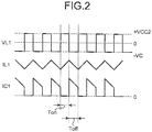
FIG. 2 is a diagram illustrating an operation example of the switching control device according to the embodiment. -
FIG. 3 is a circuit diagram illustrating a configuration example of a switching control device according to a modification. -
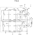
FIG. 4 is a circuit diagram illustrating a configuration example of a switching control device according to a modification. - A mode (embodiment) for carrying out the present invention will be described in detail with reference to the drawings. The present invention is not limited by the contents described in the following embodiments. Further, the components described below include those which can be easily conceived by those skilled in the art and those which are substantially the same. Further, the configurations described below can be combined as appropriate. In addition, various omissions, substitutions, or modifications of the configuration can be made without departing from the scope of the present invention.
- A DC/
DC converter 1 according to the embodiment will be described. As illustrated inFIG. 1 , the DC/DC converter 1 is, for example, an isolated switching power supply. The DC/DC converter 1 transforms a voltage of DC power supplied from a DC power supply (battery) of a vehicle, for example. The DC/DC converter 1 includes aprimary circuit 10, a secondary circuit (not illustrated), and aswitching control device 20 that controls theprimary circuit 10. Theprimary circuit 10 includes aswitching circuit 11 and aprimary winding 12 connected to theswitching circuit 11. Theswitching circuit 11 is a circuit which is connected to the DC power supply VPP to be transformed and converts the DC power supplied from the DC power supply VPP into AC power. Here, the DC power supply VPP is a relatively high voltage, for example, a voltage of about 100 V to 200 V. Theswitching circuit 11 is, for example, a full bridge circuit configured by four switching elements. InFIG. 1 , two switching elements Q1 and Q2 are illustrated in aswitching circuit 11, and the remaining two switching elements are not illustrated. Each of the switching elements Q1 and Q2 is, for example, an N-channel type Metal-Oxide-Semiconductor Field-Effect Transistor (MOSFET), and hereinafter, also simply referred to as FETs Q1 and Q2. A drain terminal d1 as an input terminal of the FET Q1 is connected to the power supply VPP. A secondary circuit (not illustrated) includes a secondary wiring installed opposite to aprimary winding 12, a rectifying circuit connected to the secondary wiring and rectifying the AC power output from the secondary wiring into DC power, and a smoothing circuit connected to the rectifying circuit and smoothing DC current output from the rectifying circuit. The DC/DC converter 1 converts DC power supplied from the DC power supply VPP into AC power by aswitching circuit 11, transforms the converted AC power by theprimary winding 12 and the secondary winding, rectifies the transformed AC power by the rectifying circuit, smooths the DC power rectified by the rectifying circuit by a smoothing circuit, and supplies the same to a load part. - A
switching control device 20 is a device that controls four switching elements (FETs Q1, Q2, and the like) of aswitching circuit 11. Theswitching control device 20 includes adrive circuit 21 and areverse bias circuit 22 for each switching element. For example, theswitching control device 20 includes adrive circuit 21A that controls the FET Q1 of theswitching circuit 11 and areverse bias circuit 22A, and includes adrive circuit 21B that controls the FET Q2 of theswitching circuit 11 and areverse bias circuit 22B. Since the fourdrive circuits 21 have the same configuration, thedrive circuits switching circuit 11 are illustrated, and thedrive circuits 21 for controlling the remaining two switching elements of theswitching circuit 11 are not illustrated. Similarly, since the fourreverse bias circuits 22 have the same configuration,reverse bias circuits switching circuit 11 are illustrated, and thereverse bias circuits 22 for controlling the remaining two switching elements of theswitching circuit 11 are not illustrated. Since a configuration and an operation of thedrive circuit 21A for driving the FET Q1 are the same as those of thedrive circuit 21B for driving the FET Q2 in theswitching control device 20, thedrive circuit 21A will be described in detail, and the description of thedrive circuit 21B will be omitted in the following description. Further, since a configuration and an operation of thereverse bias circuit 22A applying the reverse bias voltage to the FET Q1 are the same as those of thereverse bias circuit 22B applying the reverse bias voltage to the FET Q2 in theswitching control device 20, thereverse bias circuit 22A will be described in detail, and the description of thereverse bias circuit 22B will be omitted in the following description. - The
drive circuit 21A is a circuit that controls the FET Q1 of theswitching circuit 11 to be on or off. Thedrive circuit 21A includes aprimary drive circuit 211 and asecondary drive circuit 212. Theprimary drive circuit 211 includes a power supply VCC of a low voltage (for example, about 12 V), an npn bipolar transistor Q3 (hereinafter, also simply referred to as a transistor Q3), and a pnp bipolar transistor Q4 (hereinafter, simply referred to as a transistor Q4), a primary winding PT1, a resistor R1, and capacitors C1 and C2. The transistor Q3 has a collector terminal connected to the power supply VCC, and an emitter terminal connected to an emitter terminal of the transistor Q4. A connection point of the transistor Q3 and the transistor Q4 is connected to one end of the primary winding PT1 via a resistor R1. The other end of the primary winding PT1 is connected to one end of the capacitor C1. The other end of the capacitor C1 and the collector terminal of the transistor Q4 are connected to the ground. A base terminal of the transistor Q3 and a base terminal of the transistor Q4 are connected to a pulse output circuit (not illustrated). The capacitor C2 is connected to the power supply VCC and stabilizes a power supplied from the power supply VCC. Theprimary drive circuit 211 performs an ON/OFF control of the transistors Q3 and Q4 based on a pulse signal output from a pulse output circuit, and outputs AC power (pulse signal) to the primary winding PT1. - The
secondary drive circuit 212 includes a secondary winding PT2, a power supply VCC2 of a low voltage (for example, about 12 V), a diode D1, an N-channel MOSFET Q5 (hereinafter, also simply referred to as an FET Q5), a P-channel MOSFET Q6 (hereinafter, also simply referred to as an FET Q6), and a capacitor C3. The primary winding PT1 and the secondary winding PT2 isolate theprimary drive circuit 211 and thesecondary drive circuit 212, and constitute a pulse transformer for generating a pulse signal. A gate terminal of the FET Q5 and a gate terminal of the FET Q6 are connected to one end of the secondary winding PT2. The FET Q5 has a drain terminal connected to the power supply VCC2 via the diode D1 and a source terminal connected to the drain terminal of the FET Q6. A connection point of the FET Q5 and the FET Q6 is connected to a gate terminal g1 as a control terminal of the FET Q1 via a resistor R2. A source terminal of the FET Q6 is connected between the other end of the secondary winding PT2 and a capacitor C4. Thesecondary drive circuit 212 performs an ON/OFF control of the FETs Q5 and Q6 based on an AC power (pulse signal) output via the secondary winding PT2 to apply a voltage to the gate terminal g1 of the FET Q1. - The
reverse bias circuit 22A includes a capacitor C4 and a coil L1. The capacitor C4 has one end connected to a source terminal s1 as an output terminal of the FET Q1, and the other end connected to the other end of the secondary winding PT2. The coil L1 has one end connected between a source terminal of the FET Q5 and the gate terminal g1 of the FET Q1 and the other end connected between the capacitor C4 and the source terminal s1 of the FET Q1. - In the
reverse bias circuit 22A, energy is stored in the coil L1 when the FET Q5 is turned on and the FET Q6 is turned off. Further, when the FET Q5 is turned off and the FET Q6 is turned on, thereverse bias circuit 22A discharges the energy stored in the coil L1, and charges the capacitor C4 with the discharged energy. Thereverse bias circuit 22A applies a voltage to the source terminal s1 of the FET Q1 by the energy charged in the capacitor C4 to turns the FET Q1 into a reverse bias state. - The coil L1 preferably has an inductance value by which a continuous mode can be realized in which a reverse bias voltage is continuously output when the FET Q1 is turned off. Therefore, in order to realize the continuous mode, the coil L1 preferably has an inductance value that satisfies the following equation (1). That is, when the inductance value of the coil L1 is L, the voltage applied to the
drive circuit 21A is VCC2, and an ON period per cycle when a voltage is applied to the gate terminal g1 by thedrive circuit 21A is Ton, an OFF period per cycle when no voltage is applied to the gate terminal g1 by thedrive circuit 21A is Toff, and a current value of the gate terminal g1 is IG, the coil L1 satisfies the following equation (1):
- When the coil L1 does not satisfy the inductance value of the equation (1), it turns into an intermittent mode where the reverse bias voltage is intermittently output, but it is possible to apply the reverse bias voltage to the FET Q1 even in the intermittent mode.
- Next, an example in which the
switching control device 20 controls the FET Q1 will be described. As illustrated inFIG. 2 , when the FET Q1 is turned on by thedrive circuit 21A in the switchingcontrol device 20, an energy is stored in the coil L1 of thereverse bias circuit 22A (the period Ton). At this time, in thereverse bias circuit 22A, a voltage VL1 of the coil L1 becomes +VCC2, and a current IL1 flowing through the coil L1 increases. In this case, in thereverse bias circuit 22A, a current IC1 does not flow through the capacitor C4. Then, when the FET Q1 is turned off by thedrive circuit 21A in the switchingcontrol device 20, the energy stored in the coil L1 of thereverse bias circuit 22A is discharged (the period Toff). At this time, in thereverse bias circuit 22A, the voltage VL1 of the coil L1 becomes -VC, the current IC1 flows through the capacitor C4, and the capacitor C4 is charged with energy. Then, thereverse bias circuit 22A turns the FET Q1 into a reverse bias state by the energy charged in the capacitor C4. - As described above, the switching
control device 20 according to the embodiment includes thedrive circuit 21 and thereverse bias circuit 22. For example, thedrive circuit 21A, which is an FET Q1 connected to a DC power supply VPP to be transformed and controlled to be turned on or off, is connected to the gate terminal g1 of the FET Q1 having the drain terminal d1 to which a current is input, a source terminal s1 for outputting current input from the drain terminal d1, and the gate terminal g1 for controlling the current flowing from the drain terminal d1 to the source terminal s1, and applies the voltage to the gate terminal g1 to turn on the FET Q1. Thereverse bias circuit 22A includes the capacitor C4 connected to the source terminal s1 of the FET Q1, and the coil L1 having one end connected between thedrive circuit 21A and the gate terminal g1 and the other end connected between the capacitor C4 and the source terminal s1. - Thus, when the FET Q1 is turned on by applying the voltage to the gate terminal g1 of the FET Q1 by the
drive circuit 21A, the switchingcontrol device 20 can store energy in the coil L1. Then, when the FET Q1 is turned off by thedrive circuit 21A in the switchingcontrol device 20, the energy stored in the coil L1 of thereverse bias circuit 22A may be discharged, the capacitor C4 may be charged with the discharged energy, and a reverse bias voltage can be applied to the source terminal s1 of the FET Q1 by the energy charged in the capacitor C4. As a result, the switchingcontrol device 20 can eliminate at once carriers existing between the drain terminal d1 and the source terminal s1 of the FET Q1, quickly turning off the FET Q1. Further, in the switchingcontrol device 20, since thereverse bias circuit 22A can be configured with the coil L1 and the capacitor C4, thereverse bias circuit 22A can be configured with a relatively small number of components, and it is possible to suppress an increase in the number of the components constituting thereverse bias circuit 22A. As a result, the switchingcontrol device 20 can suppress the circuit from being enlarged and suppress a manufacturing cost. - Further, when the inductance value of the coil L1 is L, the voltage applied to the
drive circuit 21A is VCC2, the ON period per period when the voltage is applied to the gate terminal g1 by thedrive circuit 21A is Ton, the OFF period per cycle when no voltage is applied to the gate terminal g1 by thedrive circuit 21A is Toff, and the current value of the gate terminal g1 is IG in the switchingcontrol device 20, the following equation (1) is satisfied:
- Thus, the switching
control device 20 can realize a continuous mode in which the reverse bias voltage is continuously output when the FET Q1 is off, and apply the reverse bias voltage to the FET Q1 stably. - Next, a modification of the embodiment will be described. Although an example in which the pulse transformer is configured with the primary winding PT1 and the secondary winding PT2 in the
drive circuit 21A has been described, the embodiment is not limited thereto. For example, as illustrated inFIG. 3 , thedrive circuit 21A may use aphotocoupler 21a instead of the pulse transformer. In this case, in adrive circuit 21C, thephotocoupler 21a includes alight emitting element 21b and alight receiving element 21c. Thelight emitting element 21b is, for example, a light emitting diode, and has an anode terminal connected between a transistor Q3 and a transistor Q4 via a resistor R1 and a cathode terminal connected to the ground. Thelight receiving element 21c is, for example, a phototransistor, and has one end connected to a gate terminal of an FET Q5 and a gate terminal of an FET Q6 and the other end connected to the capacitor C4. In thedrive circuit 21C, an optical signal is output from thelight emitting element 21b when the current flows through thelight emitting element 21b, and the optical signal output from thelight emitting element 21b is received by thelight receiving element 21c. Then, thedrive circuit 21C converts the received light signal into an electric signal (pulse signal) and outputs it to the gate terminal of the FET Q5 and the gate terminal of the FET Q6 to perform an ON/OF control of the FETs Q5 and Q6. As described above, thedrive circuit 21C may be configured to have thephotocoupler 21a. - Further, as illustrated in
FIG. 4 , thedrive circuit 21 may be configured with an Integrated Circuit (IC)circuit 21d. In this case, adrive circuit 21D includes, as theIC circuit 21d on the primary side, an input terminal IN connected to the pulse output circuit, a power supply terminal VCC1 connected to a power supply VCC, and a ground terminal GND1 connected to the ground. Further, thedrive circuit 21D includes, as anIC circuit 21d on the secondary side, an output terminal OUT connected to the gate terminal g1 of the FET Q1, a power supply terminal VCC3 connected to the power supply VCC2, and a ground terminal GND2 connected to the ground. In thedrive circuit 21D, the input terminal IN and the output terminal OUT are isolated. When an ON signal is input from the pulse output circuit to the input terminal IN, thedrive circuit 21D outputs an electrical signal that is applied to the gate terminal g1 of the FET Q1 from the output terminal OUT. Thus, thedrive circuit 21D may be configured to have theIC circuit 21d. - Further, although an example in which each of the FETs Q1, Q2 and the like of the switching
circuit 11 is the MOSFET has been described, it is not limited thereto. Each of the FETs Q1 and Q2, and the like may be, for example, a transistor such as a bipolar transistor. - Although the switching
circuit 11 has been described as a full bridge system, it is not limited thereto, and may be a half bridge system, a push-pull system, or the like. - Further, although an example in which the DC/
DC converter 1 is the isolated DC/DC converter has been described, it may be a non-isolated DC/DC converter. -
- 20
- SWITCHING CONTROL DEVICE
- 21, 21A, 21B, 21C, 21D
- DRIVE CIRCUIT
- 22, 22A, 22B
- REVERSE BIAS CIRCUIT
- VPP
- DC POWER SUPPLY
- Q1, Q2
- MOSFET (SWITCHING ELEMENT)
- d1
- DRAIN TERMINAL (INPUT TERMINAL)
- s1
- SOURCE TERMINAL (OUTPUT TERMINAL)
- g1
- GATE TERMINAL (CONTROL TERMINAL)
- L1
- COIL
- C4
- CAPACITOR
Claims (2)
- A switching control device comprising:a drive circuit that is connected to a control terminal of a switching element connected to a DC power supply to be transformed and controlled to be turned on or off, and applies a voltage to the control terminal to turn on the switching element, the switching element including an input terminal to which a current is input, an output terminal that outputs the current input from the input terminal, and the control terminal that controls the current flowing from the input terminal to the output terminal; anda reverse bias circuit that includes a capacitor connected to the output terminal, and a coil having one end connected between the drive circuit and the control terminal and the other end connected between the capacitor and the output terminal.
- The switching control device according to claim 1, wherein
when an inductance value of the coil is L, a voltage applied to the drive circuit is VCC2, an ON period per cycle during which the voltage is applied to the control terminal by the drive circuit is Ton, an OFF period per cycle during which the voltage is not applied to the control terminal by the drive circuit is Toff, and a current value of the control terminal is IG, the following equation (1) is satisfied:
Applications Claiming Priority (2)
| Application Number | Priority Date | Filing Date | Title |
|---|---|---|---|
| JP2017054649A JP6653285B2 (en) | 2017-03-21 | 2017-03-21 | Switching control device |
| PCT/JP2017/043875 WO2018173381A1 (en) | 2017-03-21 | 2017-12-06 | Switching control device |
Publications (3)
| Publication Number | Publication Date |
|---|---|
| EP3605811A1 true EP3605811A1 (en) | 2020-02-05 |
| EP3605811A4 EP3605811A4 (en) | 2020-03-04 |
| EP3605811B1 EP3605811B1 (en) | 2022-06-15 |
Family
ID=63584261
Family Applications (1)
| Application Number | Title | Priority Date | Filing Date |
|---|---|---|---|
| EP17902287.6A Active EP3605811B1 (en) | 2017-03-21 | 2017-12-06 | Switching control device |
Country Status (5)
| Country | Link |
|---|---|
| US (1) | US10770984B2 (en) |
| EP (1) | EP3605811B1 (en) |
| JP (1) | JP6653285B2 (en) |
| CN (1) | CN110326200B (en) |
| WO (1) | WO2018173381A1 (en) |
Families Citing this family (2)
| Publication number | Priority date | Publication date | Assignee | Title |
|---|---|---|---|---|
| CA3154854A1 (en) * | 2019-09-16 | 2021-03-25 | Lasermotive, Inc. | Optical power for electronic switches |
| US11082033B2 (en) * | 2019-10-25 | 2021-08-03 | Texas Instruments Incorporated | Rapid and high voltage pulse generation circuits |
Family Cites Families (25)
| Publication number | Priority date | Publication date | Assignee | Title |
|---|---|---|---|---|
| US4488210A (en) * | 1982-04-07 | 1984-12-11 | Sanyo Electric Co., Ltd. | Power supply circuit of switching regulator type |
| US5010261A (en) * | 1989-12-08 | 1991-04-23 | General Electric Company | Lossless gate driver circuit for a high frequency converter |
| JPH0494825U (en) * | 1991-01-16 | 1992-08-18 | ||
| US5264736A (en) * | 1992-04-28 | 1993-11-23 | Raytheon Company | High frequency resonant gate drive for a power MOSFET |
| JPH0637614A (en) | 1992-07-20 | 1994-02-10 | Toyota Autom Loom Works Ltd | Driving circuit for current driving type semiconductor switching element |
| US5276357A (en) * | 1992-09-01 | 1994-01-04 | Broadcast Electronics, Inc. | High efficiency quasi-square wave drive circuit for switching power amplifiers |
| JP3250308B2 (en) * | 1993-03-23 | 2002-01-28 | 松下電器産業株式会社 | Gate drive circuit |
| JPH0716592U (en) * | 1993-08-25 | 1995-03-17 | 株式会社アマダ | Field effect transistor gate circuit |
| JP3391999B2 (en) * | 1996-12-24 | 2003-03-31 | 松下電工株式会社 | Power circuit |
| US6677828B1 (en) * | 2000-08-17 | 2004-01-13 | Eni Technology, Inc. | Method of hot switching a plasma tuner |
| US6650169B2 (en) * | 2001-10-01 | 2003-11-18 | Koninklijke Philips Electronics N.V. | Gate driver apparatus having an energy recovering circuit |
| US6570777B1 (en) * | 2001-12-06 | 2003-05-27 | Eni Technology, Inc. | Half sine wave resonant drive circuit |
| JP4321330B2 (en) * | 2003-07-02 | 2009-08-26 | 株式会社デンソー | Gate drive circuit |
| US7598792B2 (en) * | 2005-01-31 | 2009-10-06 | Queen's University At Kingston | Resonant gate drive circuits |
| JP4895732B2 (en) | 2006-09-06 | 2012-03-14 | 新電元工業株式会社 | Switching power supply |
| US7960997B2 (en) * | 2007-08-08 | 2011-06-14 | Advanced Analogic Technologies, Inc. | Cascode current sensor for discrete power semiconductor devices |
| JP5217849B2 (en) * | 2008-09-29 | 2013-06-19 | サンケン電気株式会社 | Electrical circuit switching device |
| JP4787350B2 (en) * | 2009-10-14 | 2011-10-05 | Smk株式会社 | Self-excited switching power supply circuit |
| US8593209B2 (en) * | 2010-12-15 | 2013-11-26 | Eaton Corporation | Resonant tank drive circuits for current-controlled semiconductor devices |
| JP5580782B2 (en) * | 2011-06-06 | 2014-08-27 | 住友電気工業株式会社 | Switching circuit |
| US8456201B2 (en) * | 2011-07-06 | 2013-06-04 | Eaton Corporation | Energy-recycling resonant drive circuits for semiconductor devices |
| JP6255997B2 (en) * | 2013-12-27 | 2018-01-10 | 富士通株式会社 | Semiconductor device |
| US9755425B2 (en) * | 2014-03-28 | 2017-09-05 | Infineon Technologies Ag | Power switch device |
| JP6513245B2 (en) * | 2017-03-02 | 2019-05-15 | 株式会社日立製作所 | Circuit for controlling gate current of semiconductor switching device |
| US10250249B1 (en) * | 2017-06-30 | 2019-04-02 | Bel Power Solutions Inc. | Recuperative gate drive circuit and method |
-
2017
- 2017-03-21 JP JP2017054649A patent/JP6653285B2/en active Active
- 2017-12-06 WO PCT/JP2017/043875 patent/WO2018173381A1/en not_active Ceased
- 2017-12-06 CN CN201780087126.9A patent/CN110326200B/en active Active
- 2017-12-06 EP EP17902287.6A patent/EP3605811B1/en active Active
-
2019
- 2019-08-20 US US16/546,182 patent/US10770984B2/en active Active
Also Published As
| Publication number | Publication date |
|---|---|
| JP6653285B2 (en) | 2020-02-26 |
| EP3605811A4 (en) | 2020-03-04 |
| EP3605811B1 (en) | 2022-06-15 |
| WO2018173381A1 (en) | 2018-09-27 |
| CN110326200B (en) | 2021-04-23 |
| US20190372467A1 (en) | 2019-12-05 |
| CN110326200A (en) | 2019-10-11 |
| JP2018157728A (en) | 2018-10-04 |
| US10770984B2 (en) | 2020-09-08 |
Similar Documents
| Publication | Publication Date | Title |
|---|---|---|
| CN104767360B (en) | System and method for driving switch | |
| CN111010040B (en) | Synchronous rectification control device, insulated synchronous rectification type DC/DC converter, gate drive device, and AC/DC converter | |
| US10404180B2 (en) | Driver circuit for switch | |
| US10361698B2 (en) | Transformer based gate drive circuit | |
| EP3151408A2 (en) | Tapped winding flyback converter for multiple output voltages | |
| US10673342B1 (en) | Active clamping with bootstrap circuit | |
| US10418906B2 (en) | High efficiency primary and secondary bias flyback converter with dual outputs | |
| EP1229635A2 (en) | Active gate clamp circuit for self driven synchronous rectifiers | |
| JP2024154500A (en) | Power source device | |
| JP2019041431A (en) | Power reception device | |
| US11258441B2 (en) | Drive circuit | |
| EP3605811B1 (en) | Switching control device | |
| US20230275526A1 (en) | Rectifying element and voltage converter comprising such a rectifying element | |
| US20060139967A1 (en) | Synchronous rectifier drive circuit for low output voltage active clamp forward converter | |
| US10644688B2 (en) | Biasing circuit for switch | |
| US20230327664A1 (en) | Switching circuit apparatus capable of controlling multiple switching elements to synchronously turn on and off with bootstrap circuit | |
| US11611284B2 (en) | Isolated switching power converter with multiple outputs | |
| JP4669341B2 (en) | Charge pump circuit for switching power supply | |
| EP3361614A1 (en) | High side driver without dedicated supply in high voltage applications | |
| JP7286295B2 (en) | Gate drive devices, isolated DC/DC converters, AC/DC converters, power adapters and electrical equipment |
Legal Events
| Date | Code | Title | Description |
|---|---|---|---|
| STAA | Information on the status of an ep patent application or granted ep patent |
Free format text: STATUS: THE INTERNATIONAL PUBLICATION HAS BEEN MADE |
|
| PUAI | Public reference made under article 153(3) epc to a published international application that has entered the european phase |
Free format text: ORIGINAL CODE: 0009012 |
|
| STAA | Information on the status of an ep patent application or granted ep patent |
Free format text: STATUS: REQUEST FOR EXAMINATION WAS MADE |
|
| 17P | Request for examination filed |
Effective date: 20190819 |
|
| AK | Designated contracting states |
Kind code of ref document: A1 Designated state(s): AL AT BE BG CH CY CZ DE DK EE ES FI FR GB GR HR HU IE IS IT LI LT LU LV MC MK MT NL NO PL PT RO RS SE SI SK SM TR |
|
| AX | Request for extension of the european patent |
Extension state: BA ME |
|
| A4 | Supplementary search report drawn up and despatched |
Effective date: 20200131 |
|
| RIC1 | Information provided on ipc code assigned before grant |
Ipc: H03K 17/0412 20060101ALI20200124BHEP Ipc: H03K 17/687 20060101ALI20200124BHEP Ipc: H03K 17/042 20060101ALI20200124BHEP Ipc: H02M 1/08 20060101AFI20200124BHEP |
|
| DAV | Request for validation of the european patent (deleted) | ||
| DAX | Request for extension of the european patent (deleted) | ||
| STAA | Information on the status of an ep patent application or granted ep patent |
Free format text: STATUS: EXAMINATION IS IN PROGRESS |
|
| 17Q | First examination report despatched |
Effective date: 20201125 |
|
| GRAP | Despatch of communication of intention to grant a patent |
Free format text: ORIGINAL CODE: EPIDOSNIGR1 |
|
| STAA | Information on the status of an ep patent application or granted ep patent |
Free format text: STATUS: GRANT OF PATENT IS INTENDED |
|
| RIC1 | Information provided on ipc code assigned before grant |
Ipc: H03K 17/785 20060101ALI20220309BHEP Ipc: H03K 17/691 20060101ALI20220309BHEP Ipc: H03K 17/0412 20060101ALI20220309BHEP Ipc: H03K 17/042 20060101ALI20220309BHEP Ipc: H03K 17/687 20060101ALI20220309BHEP Ipc: H02M 1/08 20060101AFI20220309BHEP |
|
| INTG | Intention to grant announced |
Effective date: 20220407 |
|
| GRAS | Grant fee paid |
Free format text: ORIGINAL CODE: EPIDOSNIGR3 |
|
| GRAA | (expected) grant |
Free format text: ORIGINAL CODE: 0009210 |
|
| STAA | Information on the status of an ep patent application or granted ep patent |
Free format text: STATUS: THE PATENT HAS BEEN GRANTED |
|
| AK | Designated contracting states |
Kind code of ref document: B1 Designated state(s): AL AT BE BG CH CY CZ DE DK EE ES FI FR GB GR HR HU IE IS IT LI LT LU LV MC MK MT NL NO PL PT RO RS SE SI SK SM TR |
|
| REG | Reference to a national code |
Ref country code: CH Ref legal event code: EP Ref country code: GB Ref legal event code: FG4D |
|
| REG | Reference to a national code |
Ref country code: IE Ref legal event code: FG4D |
|
| REG | Reference to a national code |
Ref country code: DE Ref legal event code: R096 Ref document number: 602017058659 Country of ref document: DE |
|
| REG | Reference to a national code |
Ref country code: AT Ref legal event code: REF Ref document number: 1498999 Country of ref document: AT Kind code of ref document: T Effective date: 20220715 |
|
| REG | Reference to a national code |
Ref country code: LT Ref legal event code: MG9D |
|
| REG | Reference to a national code |
Ref country code: NL Ref legal event code: MP Effective date: 20220615 |
|
| PG25 | Lapsed in a contracting state [announced via postgrant information from national office to epo] |
Ref country code: SE Free format text: LAPSE BECAUSE OF FAILURE TO SUBMIT A TRANSLATION OF THE DESCRIPTION OR TO PAY THE FEE WITHIN THE PRESCRIBED TIME-LIMIT Effective date: 20220615 Ref country code: NO Free format text: LAPSE BECAUSE OF FAILURE TO SUBMIT A TRANSLATION OF THE DESCRIPTION OR TO PAY THE FEE WITHIN THE PRESCRIBED TIME-LIMIT Effective date: 20220915 Ref country code: LT Free format text: LAPSE BECAUSE OF FAILURE TO SUBMIT A TRANSLATION OF THE DESCRIPTION OR TO PAY THE FEE WITHIN THE PRESCRIBED TIME-LIMIT Effective date: 20220615 Ref country code: HR Free format text: LAPSE BECAUSE OF FAILURE TO SUBMIT A TRANSLATION OF THE DESCRIPTION OR TO PAY THE FEE WITHIN THE PRESCRIBED TIME-LIMIT Effective date: 20220615 Ref country code: GR Free format text: LAPSE BECAUSE OF FAILURE TO SUBMIT A TRANSLATION OF THE DESCRIPTION OR TO PAY THE FEE WITHIN THE PRESCRIBED TIME-LIMIT Effective date: 20220916 Ref country code: FI Free format text: LAPSE BECAUSE OF FAILURE TO SUBMIT A TRANSLATION OF THE DESCRIPTION OR TO PAY THE FEE WITHIN THE PRESCRIBED TIME-LIMIT Effective date: 20220615 Ref country code: BG Free format text: LAPSE BECAUSE OF FAILURE TO SUBMIT A TRANSLATION OF THE DESCRIPTION OR TO PAY THE FEE WITHIN THE PRESCRIBED TIME-LIMIT Effective date: 20220915 |
|
| REG | Reference to a national code |
Ref country code: AT Ref legal event code: MK05 Ref document number: 1498999 Country of ref document: AT Kind code of ref document: T Effective date: 20220615 |
|
| PG25 | Lapsed in a contracting state [announced via postgrant information from national office to epo] |
Ref country code: RS Free format text: LAPSE BECAUSE OF FAILURE TO SUBMIT A TRANSLATION OF THE DESCRIPTION OR TO PAY THE FEE WITHIN THE PRESCRIBED TIME-LIMIT Effective date: 20220615 Ref country code: LV Free format text: LAPSE BECAUSE OF FAILURE TO SUBMIT A TRANSLATION OF THE DESCRIPTION OR TO PAY THE FEE WITHIN THE PRESCRIBED TIME-LIMIT Effective date: 20220615 |
|
| PG25 | Lapsed in a contracting state [announced via postgrant information from national office to epo] |
Ref country code: NL Free format text: LAPSE BECAUSE OF FAILURE TO SUBMIT A TRANSLATION OF THE DESCRIPTION OR TO PAY THE FEE WITHIN THE PRESCRIBED TIME-LIMIT Effective date: 20220615 |
|
| PG25 | Lapsed in a contracting state [announced via postgrant information from national office to epo] |
Ref country code: SM Free format text: LAPSE BECAUSE OF FAILURE TO SUBMIT A TRANSLATION OF THE DESCRIPTION OR TO PAY THE FEE WITHIN THE PRESCRIBED TIME-LIMIT Effective date: 20220615 Ref country code: SK Free format text: LAPSE BECAUSE OF FAILURE TO SUBMIT A TRANSLATION OF THE DESCRIPTION OR TO PAY THE FEE WITHIN THE PRESCRIBED TIME-LIMIT Effective date: 20220615 Ref country code: RO Free format text: LAPSE BECAUSE OF FAILURE TO SUBMIT A TRANSLATION OF THE DESCRIPTION OR TO PAY THE FEE WITHIN THE PRESCRIBED TIME-LIMIT Effective date: 20220615 Ref country code: PT Free format text: LAPSE BECAUSE OF FAILURE TO SUBMIT A TRANSLATION OF THE DESCRIPTION OR TO PAY THE FEE WITHIN THE PRESCRIBED TIME-LIMIT Effective date: 20221017 Ref country code: ES Free format text: LAPSE BECAUSE OF FAILURE TO SUBMIT A TRANSLATION OF THE DESCRIPTION OR TO PAY THE FEE WITHIN THE PRESCRIBED TIME-LIMIT Effective date: 20220615 Ref country code: EE Free format text: LAPSE BECAUSE OF FAILURE TO SUBMIT A TRANSLATION OF THE DESCRIPTION OR TO PAY THE FEE WITHIN THE PRESCRIBED TIME-LIMIT Effective date: 20220615 Ref country code: CZ Free format text: LAPSE BECAUSE OF FAILURE TO SUBMIT A TRANSLATION OF THE DESCRIPTION OR TO PAY THE FEE WITHIN THE PRESCRIBED TIME-LIMIT Effective date: 20220615 Ref country code: AT Free format text: LAPSE BECAUSE OF FAILURE TO SUBMIT A TRANSLATION OF THE DESCRIPTION OR TO PAY THE FEE WITHIN THE PRESCRIBED TIME-LIMIT Effective date: 20220615 |
|
| PG25 | Lapsed in a contracting state [announced via postgrant information from national office to epo] |
Ref country code: PL Free format text: LAPSE BECAUSE OF FAILURE TO SUBMIT A TRANSLATION OF THE DESCRIPTION OR TO PAY THE FEE WITHIN THE PRESCRIBED TIME-LIMIT Effective date: 20220615 Ref country code: IS Free format text: LAPSE BECAUSE OF FAILURE TO SUBMIT A TRANSLATION OF THE DESCRIPTION OR TO PAY THE FEE WITHIN THE PRESCRIBED TIME-LIMIT Effective date: 20221015 |
|
| REG | Reference to a national code |
Ref country code: DE Ref legal event code: R097 Ref document number: 602017058659 Country of ref document: DE |
|
| PG25 | Lapsed in a contracting state [announced via postgrant information from national office to epo] |
Ref country code: AL Free format text: LAPSE BECAUSE OF FAILURE TO SUBMIT A TRANSLATION OF THE DESCRIPTION OR TO PAY THE FEE WITHIN THE PRESCRIBED TIME-LIMIT Effective date: 20220615 |
|
| PLBE | No opposition filed within time limit |
Free format text: ORIGINAL CODE: 0009261 |
|
| STAA | Information on the status of an ep patent application or granted ep patent |
Free format text: STATUS: NO OPPOSITION FILED WITHIN TIME LIMIT |
|
| PG25 | Lapsed in a contracting state [announced via postgrant information from national office to epo] |
Ref country code: DK Free format text: LAPSE BECAUSE OF FAILURE TO SUBMIT A TRANSLATION OF THE DESCRIPTION OR TO PAY THE FEE WITHIN THE PRESCRIBED TIME-LIMIT Effective date: 20220615 |
|
| 26N | No opposition filed |
Effective date: 20230316 |
|
| PG25 | Lapsed in a contracting state [announced via postgrant information from national office to epo] |
Ref country code: SI Free format text: LAPSE BECAUSE OF FAILURE TO SUBMIT A TRANSLATION OF THE DESCRIPTION OR TO PAY THE FEE WITHIN THE PRESCRIBED TIME-LIMIT Effective date: 20220615 |
|
| REG | Reference to a national code |
Ref country code: CH Ref legal event code: PL |
|
| GBPC | Gb: european patent ceased through non-payment of renewal fee |
Effective date: 20221206 |
|
| REG | Reference to a national code |
Ref country code: BE Ref legal event code: MM Effective date: 20221231 |
|
| PG25 | Lapsed in a contracting state [announced via postgrant information from national office to epo] |
Ref country code: LU Free format text: LAPSE BECAUSE OF NON-PAYMENT OF DUE FEES Effective date: 20221206 |
|
| PG25 | Lapsed in a contracting state [announced via postgrant information from national office to epo] |
Ref country code: LI Free format text: LAPSE BECAUSE OF NON-PAYMENT OF DUE FEES Effective date: 20221231 Ref country code: IE Free format text: LAPSE BECAUSE OF NON-PAYMENT OF DUE FEES Effective date: 20221206 Ref country code: CH Free format text: LAPSE BECAUSE OF NON-PAYMENT OF DUE FEES Effective date: 20221231 Ref country code: GB Free format text: LAPSE BECAUSE OF NON-PAYMENT OF DUE FEES Effective date: 20221206 |
|
| PG25 | Lapsed in a contracting state [announced via postgrant information from national office to epo] |
Ref country code: FR Free format text: LAPSE BECAUSE OF NON-PAYMENT OF DUE FEES Effective date: 20221231 Ref country code: BE Free format text: LAPSE BECAUSE OF NON-PAYMENT OF DUE FEES Effective date: 20221231 |
|
| PG25 | Lapsed in a contracting state [announced via postgrant information from national office to epo] |
Ref country code: IT Free format text: LAPSE BECAUSE OF FAILURE TO SUBMIT A TRANSLATION OF THE DESCRIPTION OR TO PAY THE FEE WITHIN THE PRESCRIBED TIME-LIMIT Effective date: 20220615 |
|
| PG25 | Lapsed in a contracting state [announced via postgrant information from national office to epo] |
Ref country code: HU Free format text: LAPSE BECAUSE OF FAILURE TO SUBMIT A TRANSLATION OF THE DESCRIPTION OR TO PAY THE FEE WITHIN THE PRESCRIBED TIME-LIMIT; INVALID AB INITIO Effective date: 20171206 |
|
| PG25 | Lapsed in a contracting state [announced via postgrant information from national office to epo] |
Ref country code: CY Free format text: LAPSE BECAUSE OF FAILURE TO SUBMIT A TRANSLATION OF THE DESCRIPTION OR TO PAY THE FEE WITHIN THE PRESCRIBED TIME-LIMIT Effective date: 20220615 |
|
| PG25 | Lapsed in a contracting state [announced via postgrant information from national office to epo] |
Ref country code: MK Free format text: LAPSE BECAUSE OF FAILURE TO SUBMIT A TRANSLATION OF THE DESCRIPTION OR TO PAY THE FEE WITHIN THE PRESCRIBED TIME-LIMIT Effective date: 20220615 |
|
| PG25 | Lapsed in a contracting state [announced via postgrant information from national office to epo] |
Ref country code: MC Free format text: LAPSE BECAUSE OF FAILURE TO SUBMIT A TRANSLATION OF THE DESCRIPTION OR TO PAY THE FEE WITHIN THE PRESCRIBED TIME-LIMIT Effective date: 20220615 |
|
| PG25 | Lapsed in a contracting state [announced via postgrant information from national office to epo] |
Ref country code: MC Free format text: LAPSE BECAUSE OF FAILURE TO SUBMIT A TRANSLATION OF THE DESCRIPTION OR TO PAY THE FEE WITHIN THE PRESCRIBED TIME-LIMIT Effective date: 20220615 |
|
| PG25 | Lapsed in a contracting state [announced via postgrant information from national office to epo] |
Ref country code: MT Free format text: LAPSE BECAUSE OF FAILURE TO SUBMIT A TRANSLATION OF THE DESCRIPTION OR TO PAY THE FEE WITHIN THE PRESCRIBED TIME-LIMIT Effective date: 20220615 |
|
| PG25 | Lapsed in a contracting state [announced via postgrant information from national office to epo] |
Ref country code: BG Free format text: LAPSE BECAUSE OF FAILURE TO SUBMIT A TRANSLATION OF THE DESCRIPTION OR TO PAY THE FEE WITHIN THE PRESCRIBED TIME-LIMIT Effective date: 20220615 |
|
| PG25 | Lapsed in a contracting state [announced via postgrant information from national office to epo] |
Ref country code: BG Free format text: LAPSE BECAUSE OF FAILURE TO SUBMIT A TRANSLATION OF THE DESCRIPTION OR TO PAY THE FEE WITHIN THE PRESCRIBED TIME-LIMIT Effective date: 20220615 |
|
| PG25 | Lapsed in a contracting state [announced via postgrant information from national office to epo] |
Ref country code: TR Free format text: LAPSE BECAUSE OF FAILURE TO SUBMIT A TRANSLATION OF THE DESCRIPTION OR TO PAY THE FEE WITHIN THE PRESCRIBED TIME-LIMIT Effective date: 20220615 |
|
| PGFP | Annual fee paid to national office [announced via postgrant information from national office to epo] |
Ref country code: DE Payment date: 20251028 Year of fee payment: 9 |