EP3605767A1 - Power supply circuit - Google Patents
Power supply circuit Download PDFInfo
- Publication number
- EP3605767A1 EP3605767A1 EP19188447.7A EP19188447A EP3605767A1 EP 3605767 A1 EP3605767 A1 EP 3605767A1 EP 19188447 A EP19188447 A EP 19188447A EP 3605767 A1 EP3605767 A1 EP 3605767A1
- Authority
- EP
- European Patent Office
- Prior art keywords
- voltage
- capacitor
- power supply
- supply circuit
- diode
- Prior art date
- Legal status (The legal status is an assumption and is not a legal conclusion. Google has not performed a legal analysis and makes no representation as to the accuracy of the status listed.)
- Withdrawn
Links
- 239000003990 capacitor Substances 0.000 claims abstract description 90
- 238000010586 diagram Methods 0.000 description 15
- 238000007599 discharging Methods 0.000 description 5
- 238000009499 grossing Methods 0.000 description 5
- 230000000630 rising effect Effects 0.000 description 4
- 238000010521 absorption reaction Methods 0.000 description 2
- 230000015556 catabolic process Effects 0.000 description 1
- 230000007423 decrease Effects 0.000 description 1
Images


Classifications
-
- H—ELECTRICITY
- H02—GENERATION; CONVERSION OR DISTRIBUTION OF ELECTRIC POWER
- H02M—APPARATUS FOR CONVERSION BETWEEN AC AND AC, BETWEEN AC AND DC, OR BETWEEN DC AND DC, AND FOR USE WITH MAINS OR SIMILAR POWER SUPPLY SYSTEMS; CONVERSION OF DC OR AC INPUT POWER INTO SURGE OUTPUT POWER; CONTROL OR REGULATION THEREOF
- H02M1/00—Details of apparatus for conversion
- H02M1/32—Means for protecting converters other than automatic disconnection
-
- H—ELECTRICITY
- H02—GENERATION; CONVERSION OR DISTRIBUTION OF ELECTRIC POWER
- H02M—APPARATUS FOR CONVERSION BETWEEN AC AND AC, BETWEEN AC AND DC, OR BETWEEN DC AND DC, AND FOR USE WITH MAINS OR SIMILAR POWER SUPPLY SYSTEMS; CONVERSION OF DC OR AC INPUT POWER INTO SURGE OUTPUT POWER; CONTROL OR REGULATION THEREOF
- H02M1/00—Details of apparatus for conversion
- H02M1/36—Means for starting or stopping converters
-
- H—ELECTRICITY
- H02—GENERATION; CONVERSION OR DISTRIBUTION OF ELECTRIC POWER
- H02M—APPARATUS FOR CONVERSION BETWEEN AC AND AC, BETWEEN AC AND DC, OR BETWEEN DC AND DC, AND FOR USE WITH MAINS OR SIMILAR POWER SUPPLY SYSTEMS; CONVERSION OF DC OR AC INPUT POWER INTO SURGE OUTPUT POWER; CONTROL OR REGULATION THEREOF
- H02M3/00—Conversion of DC power input into DC power output
- H02M3/02—Conversion of DC power input into DC power output without intermediate conversion into AC
- H02M3/04—Conversion of DC power input into DC power output without intermediate conversion into AC by static converters
- H02M3/10—Conversion of DC power input into DC power output without intermediate conversion into AC by static converters using discharge tubes with control electrode or semiconductor devices with control electrode
- H02M3/145—Conversion of DC power input into DC power output without intermediate conversion into AC by static converters using discharge tubes with control electrode or semiconductor devices with control electrode using devices of a triode or transistor type requiring continuous application of a control signal
- H02M3/155—Conversion of DC power input into DC power output without intermediate conversion into AC by static converters using discharge tubes with control electrode or semiconductor devices with control electrode using devices of a triode or transistor type requiring continuous application of a control signal using semiconductor devices only
-
- H—ELECTRICITY
- H02—GENERATION; CONVERSION OR DISTRIBUTION OF ELECTRIC POWER
- H02M—APPARATUS FOR CONVERSION BETWEEN AC AND AC, BETWEEN AC AND DC, OR BETWEEN DC AND DC, AND FOR USE WITH MAINS OR SIMILAR POWER SUPPLY SYSTEMS; CONVERSION OF DC OR AC INPUT POWER INTO SURGE OUTPUT POWER; CONTROL OR REGULATION THEREOF
- H02M3/00—Conversion of DC power input into DC power output
- H02M3/02—Conversion of DC power input into DC power output without intermediate conversion into AC
- H02M3/04—Conversion of DC power input into DC power output without intermediate conversion into AC by static converters
- H02M3/10—Conversion of DC power input into DC power output without intermediate conversion into AC by static converters using discharge tubes with control electrode or semiconductor devices with control electrode
- H02M3/145—Conversion of DC power input into DC power output without intermediate conversion into AC by static converters using discharge tubes with control electrode or semiconductor devices with control electrode using devices of a triode or transistor type requiring continuous application of a control signal
- H02M3/155—Conversion of DC power input into DC power output without intermediate conversion into AC by static converters using discharge tubes with control electrode or semiconductor devices with control electrode using devices of a triode or transistor type requiring continuous application of a control signal using semiconductor devices only
- H02M3/156—Conversion of DC power input into DC power output without intermediate conversion into AC by static converters using discharge tubes with control electrode or semiconductor devices with control electrode using devices of a triode or transistor type requiring continuous application of a control signal using semiconductor devices only with automatic control of output voltage or current, e.g. switching regulators
-
- H—ELECTRICITY
- H02—GENERATION; CONVERSION OR DISTRIBUTION OF ELECTRIC POWER
- H02H—EMERGENCY PROTECTIVE CIRCUIT ARRANGEMENTS
- H02H9/00—Emergency protective circuit arrangements for limiting excess current or voltage without disconnection
- H02H9/04—Emergency protective circuit arrangements for limiting excess current or voltage without disconnection responsive to excess voltage
- H02H9/041—Emergency protective circuit arrangements for limiting excess current or voltage without disconnection responsive to excess voltage using a short-circuiting device
-
- H—ELECTRICITY
- H02—GENERATION; CONVERSION OR DISTRIBUTION OF ELECTRIC POWER
- H02M—APPARATUS FOR CONVERSION BETWEEN AC AND AC, BETWEEN AC AND DC, OR BETWEEN DC AND DC, AND FOR USE WITH MAINS OR SIMILAR POWER SUPPLY SYSTEMS; CONVERSION OF DC OR AC INPUT POWER INTO SURGE OUTPUT POWER; CONTROL OR REGULATION THEREOF
- H02M7/00—Conversion of AC power input into DC power output; Conversion of DC power input into AC power output
- H02M7/02—Conversion of AC power input into DC power output without possibility of reversal
- H02M7/04—Conversion of AC power input into DC power output without possibility of reversal by static converters
- H02M7/06—Conversion of AC power input into DC power output without possibility of reversal by static converters using discharge tubes without control electrode or semiconductor devices without control electrode
Definitions
- the present invention relates to a power supply circuit, and particularly to a step-down chopper.
- a step-down chopper is one type of a direct-current (DC)-DC converter.
- DC direct-current
- an input voltage is directly switched by a switching element.
- the DC input voltage is converted by the switching element into high-frequency electric power.
- the converted voltage is again converted into a DC voltage by a smoothing choke coil and a smoothing capacitor (see pages 92 to 93 in "Practical Power Supply Circuit Design Handbook" (the 22nd edition) by Jiro Togawa, CQ Publishing Co., Ltd., August 2003 ).
- a switching element interrupts the flow of a current.
- the current flows into a smoothing capacitor.
- the voltage on the smoothing capacitor leaps up to the level more than expected. Since the smoothing capacitor and the switching element are connected to each other, such instantaneous voltage rise may damage the switching element.
- an element for countermeasures against surge (typically, a Zener diode) needs to be inserted into a circuit.
- the operating voltage of the element for countermeasures against surge needs to be set to be lower than the rated voltage of the switching element.
- the element for countermeasures against surge may operate also during the normal operation of the step-down chopper.
- the element for countermeasures against surge When the element for countermeasures against surge is used alone, its operating voltage needs to be higher than the voltage during the normal operation of the step-down chopper, and also needs to be lower than the rated voltage of the switching element.
- a circuit element generally has characteristic variations.
- the operating voltage of the element for countermeasures against surge can also be ensured only within a specific range.
- the switching element may be damaged.
- An object of the present invention is to provide a power supply circuit that allows a switching element to be more reliably protected from a surge voltage.
- a power supply circuit includes: a coil having a first end that receives an input voltage and a second end; a switching element connected to the second end of the coil; a first capacitor connected to the second end of the coil; and a surge protection circuit connected to the second end of the coil in parallel with the first capacitor.
- the surge protection circuit includes a diode, a second capacitor, and a resistance. The diode, the second capacitor, and the resistance are connected in series to the second end of the coil.
- a power supply circuit allowing a switching element to be more reliably protected from a surge voltage can be provided.
- a surge occurs, a current flows into the first capacitor and the second capacitor. This allows absorption of the surge. Since the current flowing into the second capacitor is limited by the resistance, occurrence of an inrush current can be prevented. Thereby, a voltage rise at the second end of the coil can be suppressed. Since the voltage at the second end of the coil is applied to the switching element, the switching element can be more reliably protected from a surge voltage.
- the surge protection circuit further includes a diode. By utilizing the current/voltage characteristics of the diode, the circuit element in the power supply circuit can be protected, or the power supply circuit can be operated with stability.
- the second capacitor is larger in capacitance than the first capacitor.
- the diode is a Zener diode.
- the Zener diode has a cathode electrically connected to the second end of the coil.
- the second capacitor and the resistance are connected in series to an anode of the Zener diode.
- the Zener diode when the voltage of the first capacitor (that is, the voltage at the second end of the coil) exceeds the operating voltage of the Zener diode, the Zener diode operates. The current flows into the Zener diode and the current also flows into the second capacitor. This allows absorption of a surge.
- an operating voltage of the Zener diode is lower than a rated voltage of the switching element.
- the voltage exceeding the rated voltage of the switching element can be prevented from being applied to the switching element.
- the "operating voltage of the Zener diode” may be interchangeable with a “breakdown voltage” or a “Zener voltage”.
- an operating voltage of the Zener diode exceeds a design value of the input voltage.
- the Zener diode can be prevented from erroneously operating during the normal operation of the power supply circuit.
- the diode has an anode connected to the second end of the coil.
- charging and discharging of the second capacitor can be suppressed during the steady operation of the power supply circuit. This can consequently prevent the surge protection circuit from influencing the operation of the power supply circuit. Furthermore, the loss caused by charging and discharging of the second capacitor can also be suppressed.
- the diode has an anode connected to the second end of the coil.
- the surge protection circuit further includes a Zener diode.
- the Zener diode, the second capacitor and the resistance are connected in series to a cathode of the diode.
- charging and discharging of the second capacitor can be suppressed during the steady operation of the power supply circuit. Furthermore, the loss in the second capacitor can be suppressed.
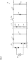
- Fig. 1 is a block diagram showing a first configuration example of a power supply circuit 10 according to the present embodiment.
- power supply circuit 10 is a step-down chopper.
- the alternating-current (AC) voltage from an AC power supply 20 is rectified by a rectifier circuit 21. Thereby, a DC voltage is input into power supply circuit 10.
- AC alternating-current
- Power supply circuit 10 includes a coil L1, a capacitor C1 (the first capacitor), a Zener diode ZD1, a capacitor C2 (the second capacitor), a resistance R1, a transistor TR1, a diode D1, a coil L2, and a capacitor C3.
- Coil L1 and capacitor C1 serve to smooth the voltage that is input into power supply circuit 10.
- Transistor TR1 serves as a switching element that switches the input voltage.
- Coil L1 has a first end connected to rectifier circuit 21 and receiving the DC input voltage.
- Transistor TR1 has a high-voltage side terminal (for example, corresponding to a collector in the case of an NPN transistor) connected to the second end of coil L1.
- Transistor TR1 has a low-voltage side terminal (an emitter in the case of an NPN transistor) connected to the first end of coil L2.
- the second end of coil L2 is connected to the output terminal and the first end of capacitor C3.
- the DC voltage input into power supply circuit 10 is converted by transistor TR1 into high-frequency electric power.
- the converted voltage is again converted into a DC voltage (a voltage Vo) by coil L2 and capacitor C3.
- switching of transistor TR1 is controlled by a control circuit.
- Diode D1 is a flywheel diode and causes the energy stored in coil L2 to circulate while transistor TR1 is OFF.
- the anode of diode D1 is connected to the second end of capacitor C3.
- the cathode of diode D1 is connected to the first end of coil L2 and the low-voltage side terminal of transistor TR1.
- Surge protection circuit 11 includes a diode, a second capacitor, and a resistance.
- the diode of surge protection circuit 11 is a Zener diode.
- the diode, the second capacitor, and the resistance are connected in series to the second end of coil L1.
- Zener diode ZD1, capacitor C2, and resistance R1 constitute surge protection circuit 11.
- Surge protection circuit 11 is connected to the second end of coil L1 in parallel with capacitor C1.
- the cathode of Zener diode ZD1 is connected to the second end of coil L1.
- Capacitor C2 and resistance R1 are connected in series to the anode of Zener diode ZD1.
- the first end of capacitor C2 is connected to the anode of Zener diode ZD1 while the first end of resistance R1 is connected to the second end of capacitor C2.
- the second end of resistance R1, the second end of capacitor C1, the anode of diode D1, and the second end of capacitor C3 are connected to a common line (a reference voltage line).
- the first end of resistance R1 may be connected to the anode of Zener diode ZD1
- capacitor C2 may be connected to the second end of resistance R1.
- resistance R1 prevents an excessively high current such as an inrush current from flowing through Zener diode ZD1 and capacitor C2. Thereby, voltage Vi is prevented from instantaneously rising. In other words, occurrence of a surge voltage in capacitor C1 can be suppressed. Accordingly, the switching element (transistor TR1) can be more reliably protected from a surge voltage.
- surge protection by surge protection circuit 11 will be described in detail.
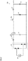
- Fig. 2 is a circuit diagram showing the basic configuration of power supply circuit 10 shown in Fig. 1 .
- a power supply circuit 10A shown in Fig. 2 is different from power supply circuit 10 in that surge protection circuit 11 is not provided.
- a current i1 flows through coil L1 for charging capacitor C1.
- Current i1 in this case is an instantaneously high current (that is, an inrush current). Since transistor TR1 is off, current i1 flows into capacitor C1.
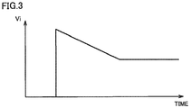
- current i1 instantaneously increases, the voltage on coil L1, that is, the voltage across capacitor C1 (voltage Vi), suddenly rises as shown in Fig. 3 .
- Voltage Vi is applied to transistor TR1.
- transistor TR1 when voltage Vi exceeds the rated voltage of transistor TR1, transistor TR1 is damaged.
- the surge voltage of capacitor C1 may be a cause of damage to transistor TR1.
- a surge protection circuit In order to suppress a sudden rising voltage (that is, a surge voltage), a surge protection circuit is generally used. Typically, a Zener diode is used as a surge protection element.
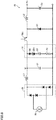
- Fig. 4 is a circuit diagram showing an example of a step-down chopper shown in Fig. 2 for which commonly-used surge countermeasures are taken.
- Zener diode ZD1 is provided in parallel with capacitor C1. Zener diode ZD1 should not operate during the normal operation of power supply circuit 10A. Thus, the operating voltage of Zener diode ZD1 should be higher than the design value of the input voltage. On the other hand, in order to protect transistor TR1, the operating voltage of Zener diode ZD1 should be lower than the rated voltage of transistor TR1.
- the rated voltage is also low.
- the difference between the input voltage during the normal operation of power supply circuit 10A and the rated voltage of transistor TR1 is relatively small.
- the input voltage during the normal operation of power supply circuit 10A (voltage Vi) is 141 V.
- the operating voltage of Zener diode ZD1 should be 180 V higher than 141 V.
- the input voltage (voltage Vi) of power supply circuit 10A is 141 V, Zener diode ZD1 does not operate. However, since the input voltage may change, there is always a possibility that the input voltage may exceed Zener voltage Vz.
- Zener voltage Vz As Zener voltage Vz is higher, the difference between the input voltage of power supply circuit 10A and Zener voltage Vz is larger, but the difference between the rated voltage of transistor TR1 and Zener voltage Vz is smaller on the contrary.
- Zener diode ZD1 has characteristic variations, Zener voltage Vz may also be higher than the rated voltage (180 V) of transistor TR1.
- Zener voltage Vz when the typical value of Zener voltage Vz is 160 V and the rated voltage of transistor TR1 is 180 V, there is no problem as long as the actual value of Zener voltage Vz shows a typical value.
- the specification value of Zener voltage Vz is defined to fall within a specific range and when the upper limit of the range exceeds the rated voltage (180 V) of transistor TR1, it is conceivable that the actual value of Zener voltage Vz may possibly exceed the rated voltage of transistor TR1.
- transistor TR1 When input voltage exceeds 180 V by using such a Zener diode as a surge protection element, transistor TR1 may be damaged.
- Fig. 6 is a diagram for illustrating surge protection in power supply circuit 10 shown in Fig. 1 .
- surge protection circuit 11 capacitor C2 and resistance R1 are connected in series to Zener diode ZD1.
- the operating voltage (Zener voltage Vz) of Zener diode ZD1 is assumed to be 150 V.
- Resistance R1 prevents an inrush current from flowing into capacitor C2. Since current i2 flows through resistance R1, a sudden rise of current i2 is suppressed. Accordingly, an instantaneously high current can be prevented from flowing into Zener diode ZD1. Furthermore, current i2 is sufficiently smaller than current i1. Thus, a sudden voltage rise by coil L1 is prevented.
- Zener diode ZD1 a capacitor having a low withstand voltage is applicable as capacitor C2.
- Fig. 7 is a block diagram showing a second configuration example of the power supply circuit according to the present embodiment.
- surge protection circuit 11 includes a diode D2 in place of Zener diode ZD1.
- Diode D2 has an anode connected to the second end of coil L1.
- Capacitor C2 and resistance R1 are connected in series to the cathode of diode D2.
- Fig. 8 is a block diagram showing a third configuration example of the power supply circuit according to the present embodiment.
- surge protection circuit 11 includes diode D2 in addition to Zener diode ZD1.
- the configuration shown in Fig. 8 is different from the configuration shown in Fig. 1 .
- the anode of diode D2 is connected to the second end of coil L1.
- the cathode of diode D2 is connected to the cathode of Zener diode ZD1.
- Capacitor C2 and resistance R1 are connected in series to the anode of Zener diode ZD1.
- Fig. 8 As in the configuration shown in Fig. 1 , input voltage Vi can be prevented from greatly rising, so that the difference between the operating voltage (Zener voltage Vz) of Zener diode ZD1 and the rated voltage of transistor TR1 can be sufficiently ensured. Furthermore, according to the configuration shown in Fig. 8 , diode D2 can prevent surge protection circuit 11 from influencing the operation of power supply circuit 10 during the steady operation of power supply circuit 10.
- the present embodiment includes the following disclosures.
- a power supply circuit (10) comprising:
- the power supply circuit (10) according to configuration 1, wherein the second capacitor (C2) is greater in capacitance than the first capacitor (C1).
- the power supply circuit (10) according to configuration 1 or configuration 2, wherein the diode is a Zener diode (ZD1), the Zener diode (ZD1) has a cathode electrically connected to the second end of the coil (L1), and the second capacitor (C2) and the resistance (R1) are connected in series to an anode of the Zener diode (ZD1).
- ZD1 Zener diode
- ZD1 has a cathode electrically connected to the second end of the coil (L1)
- the second capacitor (C2) and the resistance (R1) are connected in series to an anode of the Zener diode (ZD1).
- the power supply circuit (10) according to configuration 3, wherein an operating voltage of the Zener diode (ZD1) is lower than a rated voltage of the switching element (TR1).
- the power supply circuit (10) according to configuration 3 or configuration 4, wherein an operating voltage of the Zener diode (ZD1) exceeds a design value of the input voltage.
- the power supply circuit (10) according to configuration 1 or configuration 2, wherein the diode (D2) has an anode connected to the second end of the coil (L1).
- the power supply circuit (10) according to configuration 6, wherein the diode (D2) has an anode connected to the second end of the coil (L1), the surge protection circuit (11) further includes a Zener diode (ZD1), and the Zener diode (ZD1), the second capacitor (C2) and the resistance (R1) are connected in series to a cathode of the diode (D2).
- the diode (D2) has an anode connected to the second end of the coil (L1)
- the surge protection circuit (11) further includes a Zener diode (ZD1), and the Zener diode (ZD1), the second capacitor (C2) and the resistance (R1) are connected in series to a cathode of the diode (D2).
Landscapes
- Engineering & Computer Science (AREA)
- Power Engineering (AREA)
- Dc-Dc Converters (AREA)
- Emergency Protection Circuit Devices (AREA)
Abstract
A power supply circuit (10) includes: a coil (L1) having a first end that receives an input voltage and a second end; a transistor (TR1) connected to the second end of the coil (LI); a first capacitor (C1) connected to the second end of the coil (LI); and a surge protection circuit (11) connected to the second end of the coil (LI) in parallel with the first capacitor (C1). The surge protection circuit (11) includes a diode, a second capacitor (C2), and a resistance (R1). The diode, the second capacitor (C2), and the resistance (R1) are connected in series to the second end of the coil (LI).
Description
- The present invention relates to a power supply circuit, and particularly to a step-down chopper.
- A step-down chopper is one type of a direct-current (DC)-DC converter. In the step-down chopper, an input voltage is directly switched by a switching element. The DC input voltage is converted by the switching element into high-frequency electric power. The converted voltage is again converted into a DC voltage by a smoothing choke coil and a smoothing capacitor (see pages 92 to 93 in "Practical Power Supply Circuit Design Handbook" (the 22nd edition) by Jiro Togawa, CQ Publishing Co., Ltd., August 2003).
- At the start-up of the operation of a step-down chopper, a switching element interrupts the flow of a current. Thus, the current flows into a smoothing capacitor. When a high current instantaneously flows into a choke coil, the voltage on the smoothing capacitor leaps up to the level more than expected. Since the smoothing capacitor and the switching element are connected to each other, such instantaneous voltage rise may damage the switching element.
- In order to prevent damage to the switching element, an element for countermeasures against surge (typically, a Zener diode) needs to be inserted into a circuit. In order to protect the switching element, the operating voltage of the element for countermeasures against surge needs to be set to be lower than the rated voltage of the switching element. However, when the operating voltage of the element for countermeasures against surge is set to be relatively low, the element for countermeasures against surge may operate also during the normal operation of the step-down chopper.
- When the element for countermeasures against surge is used alone, its operating voltage needs to be higher than the voltage during the normal operation of the step-down chopper, and also needs to be lower than the rated voltage of the switching element. However, a circuit element generally has characteristic variations. Thus, the operating voltage of the element for countermeasures against surge can also be ensured only within a specific range. When the actual operating voltage of the element for countermeasures against surge exceeds the rated voltage of the switching element, the switching element may be damaged.
- An object of the present invention is to provide a power supply circuit that allows a switching element to be more reliably protected from a surge voltage.
- According to an example of the present disclosure, a power supply circuit includes: a coil having a first end that receives an input voltage and a second end; a switching element connected to the second end of the coil; a first capacitor connected to the second end of the coil; and a surge protection circuit connected to the second end of the coil in parallel with the first capacitor. The surge protection circuit includes a diode, a second capacitor, and a resistance. The diode, the second capacitor, and the resistance are connected in series to the second end of the coil.
- According to the above-described configuration, a power supply circuit allowing a switching element to be more reliably protected from a surge voltage can be provided. When a surge occurs, a current flows into the first capacitor and the second capacitor. This allows absorption of the surge. Since the current flowing into the second capacitor is limited by the resistance, occurrence of an inrush current can be prevented. Thereby, a voltage rise at the second end of the coil can be suppressed. Since the voltage at the second end of the coil is applied to the switching element, the switching element can be more reliably protected from a surge voltage. The surge protection circuit further includes a diode. By utilizing the current/voltage characteristics of the diode, the circuit element in the power supply circuit can be protected, or the power supply circuit can be operated with stability.
- In the above-described power supply circuit, the second capacitor is larger in capacitance than the first capacitor.
- According to the above-described configuration, even when the input voltage rises to thereby increase the current, the increased current flows into the second capacitor as long as the second capacitor is chargeable. Accordingly, a voltage rise across the Zener diode (between the cathode and the anode) can be suppressed, so that the Zener diode can be protected.
- In the above-described power supply circuit, the diode is a Zener diode. The Zener diode has a cathode electrically connected to the second end of the coil. The second capacitor and the resistance are connected in series to an anode of the Zener diode.
- According to the above-described configuration, when the voltage of the first capacitor (that is, the voltage at the second end of the coil) exceeds the operating voltage of the Zener diode, the Zener diode operates. The current flows into the Zener diode and the current also flows into the second capacitor. This allows absorption of a surge.
- In the above-described power supply circuit, an operating voltage of the Zener diode is lower than a rated voltage of the switching element.
- According to the above-described configuration, the voltage exceeding the rated voltage of the switching element can be prevented from being applied to the switching element. It should be noted that the "operating voltage of the Zener diode" may be interchangeable with a "breakdown voltage" or a "Zener voltage".
- In the above-described power supply circuit, an operating voltage of the Zener diode exceeds a design value of the input voltage.
- According to the above-described configuration, the Zener diode can be prevented from erroneously operating during the normal operation of the power supply circuit.
- In the above-described power supply circuit, the diode has an anode connected to the second end of the coil.
- According to the above-described configuration, charging and discharging of the second capacitor can be suppressed during the steady operation of the power supply circuit. This can consequently prevent the surge protection circuit from influencing the operation of the power supply circuit. Furthermore, the loss caused by charging and discharging of the second capacitor can also be suppressed.
- In the above-described power supply circuit, the diode has an anode connected to the second end of the coil. The surge protection circuit further includes a Zener diode. The Zener diode, the second capacitor and the resistance are connected in series to a cathode of the diode.
- According to the above-described configuration, charging and discharging of the second capacitor can be suppressed during the steady operation of the power supply circuit. Furthermore, the loss in the second capacitor can be suppressed.
- The foregoing and other objects, features, aspects and advantages of the present invention will become more apparent from the following detailed description of the present invention when taken in conjunction with the accompanying drawings.
-
-
Fig. 1 is a block diagram showing a first configuration example of a power supply circuit according to the present embodiment. -
Fig. 2 is a circuit diagram showing the basic configuration of the power supply circuit shown inFig. 1 . -
Fig. 3 is a diagram showing a schematic waveform of a surge voltage that may occur in the power supply circuit shown inFig. 1 . -
Fig. 4 is a circuit diagram showing an example of a step-down chopper shown inFig. 2 for which commonly-used surge countermeasures are taken. -
Fig. 5 is a diagram for illustrating a problem in the circuit shown inFig. 4 . -
Fig. 6 is a diagram for illustrating surge protection in the power supply circuit shown inFig. 1 . -
Fig. 7 is a block diagram showing a second configuration example of the power supply circuit according to the present embodiment. -
Fig. 8 is a block diagram showing a third configuration example of the power supply circuit according to the present embodiment. - In the following, the present embodiment will be described in detail with reference to the accompanying drawings, in which the same or corresponding components are designated by the same reference characters.
- First, an explanation will be hereinafter given with reference to
Fig. 1 with regard to an example of the situation in which the present invention is applied.Fig. 1 is a block diagram showing a first configuration example of apower supply circuit 10 according to the present embodiment. As shown inFig. 1 ,power supply circuit 10 is a step-down chopper. The alternating-current (AC) voltage from anAC power supply 20 is rectified by arectifier circuit 21. Thereby, a DC voltage is input intopower supply circuit 10. -
Power supply circuit 10 includes a coil L1, a capacitor C1 (the first capacitor), a Zener diode ZD1, a capacitor C2 (the second capacitor), a resistance R1, a transistor TR1, a diode D1, a coil L2, and a capacitor C3. Coil L1 and capacitor C1 serve to smooth the voltage that is input intopower supply circuit 10. Transistor TR1 serves as a switching element that switches the input voltage. - Coil L1 has a first end connected to
rectifier circuit 21 and receiving the DC input voltage. Transistor TR1 has a high-voltage side terminal (for example, corresponding to a collector in the case of an NPN transistor) connected to the second end of coil L1. Transistor TR1 has a low-voltage side terminal (an emitter in the case of an NPN transistor) connected to the first end of coil L2. The second end of coil L2 is connected to the output terminal and the first end of capacitor C3. - The DC voltage input into
power supply circuit 10 is converted by transistor TR1 into high-frequency electric power. The converted voltage is again converted into a DC voltage (a voltage Vo) by coil L2 and capacitor C3. Although not shown inFig. 1 , switching of transistor TR1 is controlled by a control circuit. - Diode D1 is a flywheel diode and causes the energy stored in coil L2 to circulate while transistor TR1 is OFF. Thus, the anode of diode D1 is connected to the second end of capacitor C3. Also, the cathode of diode D1 is connected to the first end of coil L2 and the low-voltage side terminal of transistor TR1.
-
Surge protection circuit 11 includes a diode, a second capacitor, and a resistance. In the first configuration example, the diode ofsurge protection circuit 11 is a Zener diode. The diode, the second capacitor, and the resistance are connected in series to the second end of coil L1. Specifically, Zener diode ZD1, capacitor C2, and resistance R1 constitutesurge protection circuit 11.Surge protection circuit 11 is connected to the second end of coil L1 in parallel with capacitor C1. The cathode of Zener diode ZD1 is connected to the second end of coil L1. Capacitor C2 and resistance R1 are connected in series to the anode of Zener diode ZD1. InFig. 1 , the first end of capacitor C2 is connected to the anode of Zener diode ZD1 while the first end of resistance R1 is connected to the second end of capacitor C2. The second end of resistance R1, the second end of capacitor C1, the anode of diode D1, and the second end of capacitor C3 are connected to a common line (a reference voltage line). Also, the first end of resistance R1 may be connected to the anode of Zener diode ZD1, and capacitor C2 may be connected to the second end of resistance R1. - At the start-up of
power supply circuit 10, a current flows through coil L1 and capacitor C1 is charged. Since transistor TR1 is stopped, the current flows into capacitor C1, so that the voltage of capacitor C1 rises. When a voltage Vi reaches the operating voltage of Zener diode ZD1, the current flows through Zener diode ZD1, so that capacitor C2 is charged. The operating voltage of Zener diode ZD1 is higher than the input voltage ofpower supply circuit 10 and lower than the rated voltage of transistor TR1. When the current flows through Zener diode ZD1, voltage Vi is maintained to be equal to or less than the rated voltage of transistor TR1, with the result that transistor TR1 can be protected. - Furthermore, resistance R1 prevents an excessively high current such as an inrush current from flowing through Zener diode ZD1 and capacitor C2. Thereby, voltage Vi is prevented from instantaneously rising. In other words, occurrence of a surge voltage in capacitor C1 can be suppressed. Accordingly, the switching element (transistor TR1) can be more reliably protected from a surge voltage. In the following, surge protection by
surge protection circuit 11 will be described in detail. -
Fig. 2 is a circuit diagram showing the basic configuration ofpower supply circuit 10 shown inFig. 1 . Apower supply circuit 10A shown inFig. 2 is different frompower supply circuit 10 in thatsurge protection circuit 11 is not provided. - At the start-up of
power supply circuit 10A, a current i1 flows through coil L1 for charging capacitor C1. Current i1 in this case is an instantaneously high current (that is, an inrush current). Since transistor TR1 is off, current i1 flows into capacitor C1. When current i1 instantaneously increases, the voltage on coil L1, that is, the voltage across capacitor C1 (voltage Vi), suddenly rises as shown inFig. 3 . - Voltage Vi is applied to transistor TR1. Thus, when voltage Vi exceeds the rated voltage of transistor TR1, transistor TR1 is damaged. The surge voltage of capacitor C1 may be a cause of damage to transistor TR1.
- In order to suppress a sudden rising voltage (that is, a surge voltage), a surge protection circuit is generally used. Typically, a Zener diode is used as a surge protection element.
-
Fig. 4 is a circuit diagram showing an example of a step-down chopper shown inFig. 2 for which commonly-used surge countermeasures are taken. As shown inFig. 4 , Zener diode ZD1 is provided in parallel with capacitor C1. Zener diode ZD1 should not operate during the normal operation ofpower supply circuit 10A. Thus, the operating voltage of Zener diode ZD1 should be higher than the design value of the input voltage. On the other hand, in order to protect transistor TR1, the operating voltage of Zener diode ZD1 should be lower than the rated voltage of transistor TR1. - From a point of view of the efficiency of
power supply circuit 10A, it is desirable to reduce the loss during switching of transistor TR1 as much as possible. Generally, in the transistor with low switching loss, the rated voltage is also low. However, when the rated voltage of transistor TR1 is low, the difference between the input voltage during the normal operation ofpower supply circuit 10A and the rated voltage of transistor TR1 is relatively small. For example, when the voltage ofAC power supply 20 is 100 VAC, a peak voltage Vpeak (and the voltage after rectification) is 141 V. Thus, the input voltage during the normal operation ofpower supply circuit 10A (voltage Vi) is 141 V. In the case ofpower supply circuit 10A shown inFig. 4 , the operating voltage of Zener diode ZD1 should be 180 V higher than 141 V. - However, when the difference between the input voltage during the normal operation of
power supply circuit 10A and the rated voltage of transistor TR1 is small, the problem as described below may occur, for example. -
Fig. 5 is a diagram for illustrating a problem in the circuit shown inFig. 4 . It is assumed that Vz = 150 V inFig. 5 . When the input voltage (voltage Vi) ofpower supply circuit 10A is 141 V, Zener diode ZD1 does not operate. However, since the input voltage may change, there is always a possibility that the input voltage may exceed Zener voltage Vz. - As Zener voltage Vz is higher, the difference between the input voltage of
power supply circuit 10A and Zener voltage Vz is larger, but the difference between the rated voltage of transistor TR1 and Zener voltage Vz is smaller on the contrary. When Zener diode ZD1 has characteristic variations, Zener voltage Vz may also be higher than the rated voltage (180 V) of transistor TR1. - For example, when the typical value of Zener voltage Vz is 160 V and the rated voltage of transistor TR1 is 180 V, there is no problem as long as the actual value of Zener voltage Vz shows a typical value. However, when the specification value of Zener voltage Vz is defined to fall within a specific range and when the upper limit of the range exceeds the rated voltage (180 V) of transistor TR1, it is conceivable that the actual value of Zener voltage Vz may possibly exceed the rated voltage of transistor TR1. When input voltage exceeds 180 V by using such a Zener diode as a surge protection element, transistor TR1 may be damaged.
-
Fig. 6 is a diagram for illustrating surge protection inpower supply circuit 10 shown inFig. 1 . Insurge protection circuit 11, capacitor C2 and resistance R1 are connected in series to Zener diode ZD1. The operating voltage (Zener voltage Vz) of Zener diode ZD1 is assumed to be 150 V. - Current i1 flows at the start-up of
power supply circuit 10. Since transistor TR1 is off, current i1 flows into capacitor C1. When voltage Vi reaches 150 V, Zener diode ZD1 operates. Thereby, a current i2 flows through Zener diode ZD1, so that capacitor C2 is charged. - Resistance R1 prevents an inrush current from flowing into capacitor C2. Since current i2 flows through resistance R1, a sudden rise of current i2 is suppressed. Accordingly, an instantaneously high current can be prevented from flowing into Zener diode ZD1. Furthermore, current i2 is sufficiently smaller than current i1. Thus, a sudden voltage rise by coil L1 is prevented.
- Furthermore, when the input voltage of
power supply circuit 10 rises due to fluctuations and the like, voltage Vi rises, so that current i2 increases. Capacitor C2 is charged by current i2. Capacitor C2 is higher in capacitance value than capacitor C1. Even when the input voltage rises to thereby increase current i2, the increased current flows into capacitor C2 as long as capacitor C2 is chargeable. Accordingly, a voltage rise across (between the cathode and the anode) of Zener diode ZD1 can be suppressed, so that Zener diode ZD1 can be protected. - According to the power supply circuit shown in
Fig. 1 , input voltage Vi can be prevented from greatly rising. Thus, the difference between the operating voltage (Zener voltage Vz) of Zener diode ZD1 and the rated voltage of transistor TR1 can be sufficiently ensured. For example, even in consideration of the variations in operating voltage of Zener diode ZD1 (for example, variations within the range of specifications), it becomes possible to increase the possibility that the operating voltage of Zener diode ZD1 is lower than the rated voltage of transistor TR1. Therefore, transistor TR1 can be protected from a surge voltage. - Furthermore, by applying Zener diode ZD1, a capacitor having a low withstand voltage is applicable as capacitor C2.
-
Fig. 7 is a block diagram showing a second configuration example of the power supply circuit according to the present embodiment. Referring toFig. 7 ,surge protection circuit 11 includes a diode D2 in place of Zener diode ZD1. In this point, the configuration shown inFig. 7 is different from the configuration shown inFig. 1 . Diode D2 has an anode connected to the second end of coil L1. Capacitor C2 and resistance R1 are connected in series to the cathode of diode D2. - At the start-up of
power supply circuit 10, voltage Vi rises and a forward current flows through diode D2. Accordingly, both capacitor C1 and capacitor C2 are charged. Thereby, a surge can be absorbed. On the other hand, transistor TR1 operates during the steady operation ofpower supply circuit 10. Thereby, the cathode-side voltage of diode D2 decreases relative to the anode-side voltage of diode D2. Since a reverse bias voltage is applied to diode D2, diode D2 is not brought into conduction. Thus, charging and discharging of capacitor C2 can be suppressed during the steady operation ofpower supply circuit 10. Furthermore, the loss caused by charging and discharging of capacitor C2 can be suppressed during the steady operation ofpower supply circuit 10. Therefore,surge protection circuit 11 can be prevented from influencing the operation ofpower supply circuit 10. -
Fig. 8 is a block diagram showing a third configuration example of the power supply circuit according to the present embodiment. Referring toFig. 8 ,surge protection circuit 11 includes diode D2 in addition to Zener diode ZD1. In this point, the configuration shown inFig. 8 is different from the configuration shown inFig. 1 . As in the configuration shown inFig. 7 , the anode of diode D2 is connected to the second end of coil L1. The cathode of diode D2 is connected to the cathode of Zener diode ZD1. Capacitor C2 and resistance R1 are connected in series to the anode of Zener diode ZD1. - According to the configuration shown in
Fig. 8 , as in the configuration shown inFig. 1 , input voltage Vi can be prevented from greatly rising, so that the difference between the operating voltage (Zener voltage Vz) of Zener diode ZD1 and the rated voltage of transistor TR1 can be sufficiently ensured. Furthermore, according to the configuration shown inFig. 8 , diode D2 can preventsurge protection circuit 11 from influencing the operation ofpower supply circuit 10 during the steady operation ofpower supply circuit 10. - As described above, the present embodiment includes the following disclosures.
- A power supply circuit (10) comprising:
- a coil (L1) having a first end that receives an input voltage and a second end;
- a switching element (TR1) connected to the second end of the coil (L1);
- a first capacitor (C1) connected to the second end of the coil (L1); and
- a surge protection circuit (11) connected to the second end of the coil (L1) in parallel with the first capacitor (C1),
- the surge protection circuit (11) including
- a diode,
- a second capacitor (C2), and
- a resistance (R1),
- the diode, the second capacitor (C2), and the resistance (R1) being connected in series to the second end of the coil (L1).
- The power supply circuit (10) according to
configuration 1, wherein the second capacitor (C2) is greater in capacitance than the first capacitor (C1). - The power supply circuit (10) according to
configuration 1 or configuration 2, wherein
the diode is a Zener diode (ZD1),
the Zener diode (ZD1) has a cathode electrically connected to the second end of the coil (L1), and
the second capacitor (C2) and the resistance (R1) are connected in series to an anode of the Zener diode (ZD1). - The power supply circuit (10) according to configuration 3, wherein an operating voltage of the Zener diode (ZD1) is lower than a rated voltage of the switching element (TR1).
- The power supply circuit (10) according to configuration 3 or configuration 4, wherein an operating voltage of the Zener diode (ZD1) exceeds a design value of the input voltage.
- The power supply circuit (10) according to
configuration 1 or configuration 2, wherein the diode (D2) has an anode connected to the second end of the coil (L1). - The power supply circuit (10) according to configuration 6, wherein
the diode (D2) has an anode connected to the second end of the coil (L1),
the surge protection circuit (11) further includes a Zener diode (ZD1), and
the Zener diode (ZD1), the second capacitor (C2) and the resistance (R1) are connected in series to a cathode of the diode (D2). - Although the present invention has been described and illustrated in detail, it is clearly understood that the same is by way of illustration and example only and is not to be taken by way of limitation, the scope of the present invention being interpreted by the terms of the appended claims.
Claims (7)
- A power supply circuit (10) comprising:a coil (L1) having a first end that receives an input voltage and a second end;a switching element (TR1) connected to the second end of the coil (L1);a first capacitor (C1) connected to the second end of the coil (L1); anda surge protection circuit (11) connected to the second end of the coil (L1) in parallel with the first capacitor (C1),the surge protection circuit (11) includinga diode,a second capacitor (C2), anda resistance (R1),the diode, the second capacitor (C2), and the resistance (R1) being connected in series to the second end of the coil (L1).
- The power supply circuit (10) according to claim 1, wherein the second capacitor (C2) is greater in capacitance than the first capacitor (C1).
- The power supply circuit (10) according to claim 1 or 2, wherein
the diode is a Zener diode (ZD1),
the Zener diode (ZD1) has a cathode electrically connected to the second end of the coil (L1), and
the second capacitor (C2) and the resistance (R1) are connected in series to an anode of the Zener diode (ZD1). - The power supply circuit (10) according to claim 3, wherein an operating voltage of the Zener diode (ZD1) is lower than a rated voltage of the switching element (TR1).
- The power supply circuit (10) according to claim 3 or 4, wherein an operating voltage of the Zener diode (ZD1) exceeds a design value of the input voltage.
- The power supply circuit (10) according to claim 1 or 2, wherein the diode (D2) has an anode connected to the second end of the coil (L1).
- The power supply circuit (10) according to claim 6, wherein
the diode (D2) has an anode connected to the second end of the coil (L1),
the surge protection circuit (11) further includes a Zener diode (ZD1), and
the Zener diode (ZD1), the second capacitor (C2) and the resistance (R1) are connected in series to a cathode of the diode (D2).
Applications Claiming Priority (2)
| Application Number | Priority Date | Filing Date | Title |
|---|---|---|---|
| JP2018146674 | 2018-08-03 | ||
| JP2019091083A JP7310284B2 (en) | 2018-08-03 | 2019-05-14 | power circuit |
Publications (1)
| Publication Number | Publication Date |
|---|---|
| EP3605767A1 true EP3605767A1 (en) | 2020-02-05 |
Family
ID=67438946
Family Applications (1)
| Application Number | Title | Priority Date | Filing Date |
|---|---|---|---|
| EP19188447.7A Withdrawn EP3605767A1 (en) | 2018-08-03 | 2019-07-25 | Power supply circuit |
Country Status (4)
| Country | Link |
|---|---|
| US (1) | US10700596B2 (en) |
| EP (1) | EP3605767A1 (en) |
| KR (1) | KR20200015380A (en) |
| CN (1) | CN110798056A (en) |
Families Citing this family (2)
| Publication number | Priority date | Publication date | Assignee | Title |
|---|---|---|---|---|
| JP7232788B2 (en) * | 2020-03-23 | 2023-03-03 | 日立Astemo株式会社 | Semiconductor devices, power modules, inverter devices, and electric vehicles |
| CN115516726A (en) * | 2020-05-22 | 2022-12-23 | 欧姆龙株式会社 | System and method for limiting inrush current during robot charging |
Citations (4)
| Publication number | Priority date | Publication date | Assignee | Title |
|---|---|---|---|---|
| US20010005322A1 (en) * | 1999-12-27 | 2001-06-28 | Akihiro Uchida | Dc-to-dc converter having an improved surge suppressor |
| EP1835609A1 (en) * | 2004-12-09 | 2007-09-19 | Daikin Industries, Ltd. | Multi-phase current supplying circuit, driving apparatus, compressor, and air conditioner |
| EP2456060A1 (en) * | 2009-07-15 | 2012-05-23 | Daikin Industries, Ltd. | Power converter circuit |
| US20160276923A1 (en) * | 2015-03-17 | 2016-09-22 | Sanken Electric Co., Ltd. | Snubber circuit |
Family Cites Families (9)
| Publication number | Priority date | Publication date | Assignee | Title |
|---|---|---|---|---|
| US4573113A (en) * | 1984-01-26 | 1986-02-25 | Borg-Warner Corporation | Surge protection system for a d-c power supply during power-up |
| CN2166534Y (en) * | 1993-08-27 | 1994-05-25 | 章光国 | Multi-plug receptacle with overcurrent overvoltage protector |
| JPH07250468A (en) * | 1994-03-11 | 1995-09-26 | Fujitsu Ltd | DC / DC converter |
| US5572397A (en) * | 1994-11-21 | 1996-11-05 | Tii Industries, Inc. | Combined overvoltage station protector apparatus having maintenance termination and half ringer circuitry |
| JP3607428B2 (en) * | 1996-08-08 | 2005-01-05 | 松下電器産業株式会社 | Fluorescent lamp lighting device |
| US8279646B1 (en) * | 2007-12-14 | 2012-10-02 | Flextronics Ap, Llc | Coordinated power sequencing to limit inrush currents and ensure optimum filtering |
| US7889526B2 (en) * | 2008-05-02 | 2011-02-15 | Lutron Electronics Co., Inc. | Cat-ear power supply having a latch reset circuit |
| CN201766500U (en) * | 2010-09-09 | 2011-03-16 | 龙驰幕墙工程有限公司 | Modified Buck circuit |
| US8929107B2 (en) * | 2011-10-21 | 2015-01-06 | Power Integrations, Inc. | Active surge protection in a power supply |
-
2019
- 2019-07-16 CN CN201910642606.8A patent/CN110798056A/en active Pending
- 2019-07-19 KR KR1020190087509A patent/KR20200015380A/en not_active Ceased
- 2019-07-25 EP EP19188447.7A patent/EP3605767A1/en not_active Withdrawn
- 2019-07-25 US US16/521,643 patent/US10700596B2/en active Active
Patent Citations (4)
| Publication number | Priority date | Publication date | Assignee | Title |
|---|---|---|---|---|
| US20010005322A1 (en) * | 1999-12-27 | 2001-06-28 | Akihiro Uchida | Dc-to-dc converter having an improved surge suppressor |
| EP1835609A1 (en) * | 2004-12-09 | 2007-09-19 | Daikin Industries, Ltd. | Multi-phase current supplying circuit, driving apparatus, compressor, and air conditioner |
| EP2456060A1 (en) * | 2009-07-15 | 2012-05-23 | Daikin Industries, Ltd. | Power converter circuit |
| US20160276923A1 (en) * | 2015-03-17 | 2016-09-22 | Sanken Electric Co., Ltd. | Snubber circuit |
Non-Patent Citations (1)
| Title |
|---|
| JIRO TOGAWA: "Practical Power Supply Circuit Design Handbook", August 2003, CQ PUBLISHING CO., LTD., pages: 92 - 93 |
Also Published As
| Publication number | Publication date |
|---|---|
| US20200044560A1 (en) | 2020-02-06 |
| US10700596B2 (en) | 2020-06-30 |
| CN110798056A (en) | 2020-02-14 |
| KR20200015380A (en) | 2020-02-12 |
Similar Documents
| Publication | Publication Date | Title |
|---|---|---|
| KR100904299B1 (en) | Power factor correction circuit and its driving method | |
| CN103812317B (en) | Clamp Snubber Circuit and Its Impedance Adjustment Method | |
| JP3415759B2 (en) | Overcurrent protection circuit for switching power supply | |
| CN109861518B (en) | Current-limiting starting circuit and power supply conversion circuit | |
| US7804271B2 (en) | Multiphase current supplying circuit, driving apparatus, compressor and air conditioner | |
| CN108347172A (en) | A kind of isolation DC-DC power module meeting GJB181 standards | |
| CN101459331A (en) | Overvoltage protection device, DC-DC voltage converter and overvoltage protection method | |
| KR20250083520A (en) | Circuit for supplying power to the control circuit of a switching power supply based on auxiliary windings | |
| GB2522646A (en) | Converter | |
| US10700596B2 (en) | Power supply circuit | |
| WO2018216401A1 (en) | Isolated switching power supply | |
| CN101379686B (en) | Method and circuit for adjusting voltage | |
| CN113690852A (en) | Switching power supply and over-power protection device and method thereof | |
| CN215452782U (en) | Voltage spike absorption circuit of switching power supply | |
| CN120264533A (en) | A flashback-proof LED driving circuit | |
| JP7310284B2 (en) | power circuit | |
| US20070024258A1 (en) | Switching power supply with voltage limiting device and control method thereof | |
| EP4300800A1 (en) | Switching power supply protection circuit and power supply system | |
| US12556086B2 (en) | Power supply apparatus with inrush current prevention circuit and boost converter circuit | |
| JP2011205810A (en) | Overvoltage protection circuit of non-insulation converter | |
| CN114336887B (en) | Power supply circuit with low cost and high reliability | |
| KR101055055B1 (en) | Power Factor Correction Circuit of Power Supply | |
| CN210297332U (en) | Control circuit with prolonged holding time and conversion system thereof | |
| Choi et al. | Protection schemes for various fault conditions for off-line flyback converters | |
| CN109617385B (en) | Capacitor precharge circuit |
Legal Events
| Date | Code | Title | Description |
|---|---|---|---|
| PUAI | Public reference made under article 153(3) epc to a published international application that has entered the european phase |
Free format text: ORIGINAL CODE: 0009012 |
|
| STAA | Information on the status of an ep patent application or granted ep patent |
Free format text: STATUS: REQUEST FOR EXAMINATION WAS MADE |
|
| STAA | Information on the status of an ep patent application or granted ep patent |
Free format text: STATUS: THE APPLICATION HAS BEEN WITHDRAWN |
|
| 17P | Request for examination filed |
Effective date: 20190725 |
|
| AK | Designated contracting states |
Kind code of ref document: A1 Designated state(s): AL AT BE BG CH CY CZ DE DK EE ES FI FR GB GR HR HU IE IS IT LI LT LU LV MC MK MT NL NO PL PT RO RS SE SI SK SM TR |
|
| AX | Request for extension of the european patent |
Extension state: BA ME |
|
| 18W | Application withdrawn |
Effective date: 20200128 |