EP3605627A1 - Piezoelectric device and method for manufacturing piezoelectric device - Google Patents
Piezoelectric device and method for manufacturing piezoelectric device Download PDFInfo
- Publication number
- EP3605627A1 EP3605627A1 EP18777140.7A EP18777140A EP3605627A1 EP 3605627 A1 EP3605627 A1 EP 3605627A1 EP 18777140 A EP18777140 A EP 18777140A EP 3605627 A1 EP3605627 A1 EP 3605627A1
- Authority
- EP
- European Patent Office
- Prior art keywords
- layer
- piezoelectric
- orientation control
- electrode
- control layer
- Prior art date
- Legal status (The legal status is an assumption and is not a legal conclusion. Google has not performed a legal analysis and makes no representation as to the accuracy of the status listed.)
- Granted
Links
Images



Classifications
-
- H—ELECTRICITY
- H10—SEMICONDUCTOR DEVICES; ELECTRIC SOLID-STATE DEVICES NOT OTHERWISE PROVIDED FOR
- H10N—ELECTRIC SOLID-STATE DEVICES NOT OTHERWISE PROVIDED FOR
- H10N30/00—Piezoelectric or electrostrictive devices
- H10N30/704—Piezoelectric or electrostrictive devices based on piezoelectric or electrostrictive films or coatings
- H10N30/706—Piezoelectric or electrostrictive devices based on piezoelectric or electrostrictive films or coatings characterised by the underlying bases, e.g. substrates
- H10N30/708—Intermediate layers, e.g. barrier, adhesion or growth control buffer layers
-
- H—ELECTRICITY
- H10—SEMICONDUCTOR DEVICES; ELECTRIC SOLID-STATE DEVICES NOT OTHERWISE PROVIDED FOR
- H10N—ELECTRIC SOLID-STATE DEVICES NOT OTHERWISE PROVIDED FOR
- H10N30/00—Piezoelectric or electrostrictive devices
- H10N30/50—Piezoelectric or electrostrictive devices having a stacked or multilayer structure
-
- H—ELECTRICITY
- H10—SEMICONDUCTOR DEVICES; ELECTRIC SOLID-STATE DEVICES NOT OTHERWISE PROVIDED FOR
- H10N—ELECTRIC SOLID-STATE DEVICES NOT OTHERWISE PROVIDED FOR
- H10N30/00—Piezoelectric or electrostrictive devices
- H10N30/01—Manufacture or treatment
- H10N30/07—Forming of piezoelectric or electrostrictive parts or bodies on an electrical element or another base
- H10N30/074—Forming of piezoelectric or electrostrictive parts or bodies on an electrical element or another base by depositing piezoelectric or electrostrictive layers, e.g. aerosol or screen printing
- H10N30/076—Forming of piezoelectric or electrostrictive parts or bodies on an electrical element or another base by depositing piezoelectric or electrostrictive layers, e.g. aerosol or screen printing by vapour phase deposition
-
- H—ELECTRICITY
- H10—SEMICONDUCTOR DEVICES; ELECTRIC SOLID-STATE DEVICES NOT OTHERWISE PROVIDED FOR
- H10N—ELECTRIC SOLID-STATE DEVICES NOT OTHERWISE PROVIDED FOR
- H10N30/00—Piezoelectric or electrostrictive devices
- H10N30/01—Manufacture or treatment
- H10N30/07—Forming of piezoelectric or electrostrictive parts or bodies on an electrical element or another base
- H10N30/074—Forming of piezoelectric or electrostrictive parts or bodies on an electrical element or another base by depositing piezoelectric or electrostrictive layers, e.g. aerosol or screen printing
- H10N30/079—Forming of piezoelectric or electrostrictive parts or bodies on an electrical element or another base by depositing piezoelectric or electrostrictive layers, e.g. aerosol or screen printing using intermediate layers, e.g. for growth control
-
- H—ELECTRICITY
- H10—SEMICONDUCTOR DEVICES; ELECTRIC SOLID-STATE DEVICES NOT OTHERWISE PROVIDED FOR
- H10N—ELECTRIC SOLID-STATE DEVICES NOT OTHERWISE PROVIDED FOR
- H10N30/00—Piezoelectric or electrostrictive devices
- H10N30/30—Piezoelectric or electrostrictive devices with mechanical input and electrical output, e.g. functioning as generators or sensors
-
- H—ELECTRICITY
- H10—SEMICONDUCTOR DEVICES; ELECTRIC SOLID-STATE DEVICES NOT OTHERWISE PROVIDED FOR
- H10N—ELECTRIC SOLID-STATE DEVICES NOT OTHERWISE PROVIDED FOR
- H10N30/00—Piezoelectric or electrostrictive devices
- H10N30/30—Piezoelectric or electrostrictive devices with mechanical input and electrical output, e.g. functioning as generators or sensors
- H10N30/302—Sensors
-
- H—ELECTRICITY
- H10—SEMICONDUCTOR DEVICES; ELECTRIC SOLID-STATE DEVICES NOT OTHERWISE PROVIDED FOR
- H10N—ELECTRIC SOLID-STATE DEVICES NOT OTHERWISE PROVIDED FOR
- H10N30/00—Piezoelectric or electrostrictive devices
- H10N30/80—Constructional details
- H10N30/85—Piezoelectric or electrostrictive active materials
- H10N30/853—Ceramic compositions
-
- H—ELECTRICITY
- H10—SEMICONDUCTOR DEVICES; ELECTRIC SOLID-STATE DEVICES NOT OTHERWISE PROVIDED FOR
- H10N—ELECTRIC SOLID-STATE DEVICES NOT OTHERWISE PROVIDED FOR
- H10N30/00—Piezoelectric or electrostrictive devices
- H10N30/80—Constructional details
- H10N30/85—Piezoelectric or electrostrictive active materials
- H10N30/857—Macromolecular compositions
-
- H—ELECTRICITY
- H10—SEMICONDUCTOR DEVICES; ELECTRIC SOLID-STATE DEVICES NOT OTHERWISE PROVIDED FOR
- H10N—ELECTRIC SOLID-STATE DEVICES NOT OTHERWISE PROVIDED FOR
- H10N30/00—Piezoelectric or electrostrictive devices
- H10N30/80—Constructional details
- H10N30/87—Electrodes or interconnections, e.g. leads or terminals
-
- H—ELECTRICITY
- H10—SEMICONDUCTOR DEVICES; ELECTRIC SOLID-STATE DEVICES NOT OTHERWISE PROVIDED FOR
- H10N—ELECTRIC SOLID-STATE DEVICES NOT OTHERWISE PROVIDED FOR
- H10N30/00—Piezoelectric or electrostrictive devices
- H10N30/80—Constructional details
- H10N30/87—Electrodes or interconnections, e.g. leads or terminals
- H10N30/877—Conductive materials
- H10N30/878—Conductive materials the principal material being non-metallic, e.g. oxide or carbon based
Definitions
- the piezoelectric layer 14 is formed over the orientation control layer 13.
- a ZnO target is used to form a film by RF magnetron sputtering in a mixed gas atmosphere of argon (Ar) and a small amount of oxygen (O 2 ).
- the film thickness of the ZnO piezoelectric layer 14 is 20 nm to 250 nm.
- the stacking 15 is formed by the orientation control layer 13 and the piezoelectric layer 14.
- the film forming temperature of ZnO is not necessarily a room temperature as long as the amorphous phase of the under layer, that is, the orientation control layer 13 is maintained during the process.
- the piezoelectric layer 14 may be formed at, for example, a substrate temperature of 150°C or below.
- the c-axis orientation is judged from measurement of X-ray rocking curve on each sample and by determining the FWHM value.
- Piezoelectric response is judged from measurement of a voltage level generated under application of a pressure onto the sample. Satisfactory piezoelectric response is indicated by a double circle ( ⁇ ), acceptable piezoelectric response is indicated by a single circle ( ⁇ ), and poor piezoelectric response is indicated by a cross mark (x).
- a 10 nm thick SAZO amorphous film is formed as the orientation control layer 13 over a 100 ⁇ m thick COP at room temperature.
- a 200 nm thick ZnO film formed as the piezoelectric layer 14 at room temperature, and a sample of 3 mm diameter (or 3 mm ⁇ 3 mm square) is fabricated.
- the film forming conditions of the respective layers are the same as those in Example 1, except for the deposition time of the piezoelectric layer 14.
- the thickness of the piezoelectric layer 14 is further increased compared with Example 3.
- the FWHM value representing the c-axis orientation of this sample is as small as 7° because of the increased thickness of the piezoelectric layer 14, and high piezoelectric response is obtained.
- the flexibility is not so high as Examples 1 and 2, but is still in the acceptable range. In the visual inspection for the evaluation of degree of cracking, no cloudiness or cracks are observed. The overall evaluation of this sample is good (marked with double circle).
- the transparency of the sample is maintained even after the haze measurement.
- the c-axis orientation is as small as 12°, and the piezoelectric response is good (with double circle).
- the overall evaluation of this sample is good (marked with double circles).
- An amorphous-phase orientation control layer 13 of a thickness of 50 nm is formed using an inorganic material SAZO on a PET film of 50 ⁇ m thickness.
- a piezoelectric layer 14 formed at a thickness of 200 nm.
- This piezoelectric layer 200 is a ZnO film that contains a 2 wt% vanadium (V) added as an dopant.
- V vanadium
- a sample of 3 mm diameter (or 3 mm ⁇ 3 mm square) is fabricated.
- the FWHM value representing the c-axis orientation of the sample of Example 18 is as small as 10°, and the piezoelectric response is also good.
- a crystal-phase orientation control layer is inserted as the underlayer of the piezoelectric layer 14.
- a crystal-phase ITO film with a thickness of 30 nm is formed as the orientation control layer 13 on the COP film of a 100 ⁇ m thickness by DC magnetron sputtering.
- the film forming conditions for the orientation control layer 13 are using the Ar/oxygen mixed gas and a 4-inch flat target, at a process pressure of 0.2 Pa and the output power of 200 W.
- the substrate temperature is set to approximately 150 °C during the sputtering process.
- FIG. 7 illustrates a configuration of a piezoelectric sensor 10B which is a modification of FIG. 1 .
- a plastic layer 18 is also disposed on the top electrode 19.
- the stacking 15 of the orientation control layer 13 and the piezoelectric layer 14 is provided between the electrode 11 and the electrode 19.
- the electrode 11 is a transparent electrode that serves as a bottom electrode
- the electrode 19 is a transparent electrode that serves as an upper electrode.
- the orientation control layer 13 is an amorphous thin film with a thickness of 3 nm to 100 nm.
- the piezoelectric layer 14 is made of a wurtzite type piezoelectric material and has a thickness of 20 nm to 250 nm.
- the piezoelectric sensor 10C has the amorphous-phase orientation control layer 13 and the piezoelectric layer 14 with an appropriate thickness, like the piezoelectric sensor 10A, and has satisfactory piezoelectric properties. Besides, the plastic layers 12 and 18 are provided under and over the stacking 15, and the device is superior in flexibility.
- the configurations of the present invention including the stacking 15 of the amorphous-phase orientation control layer 13 and the crystal-phase piezoelectric layer 14 can be applied not only to the piezoelectric sensors, but also to other piezoelectric devices such as speakers or oscillators using the inverse piezoelectric effect.
- the c-axis orientation of the piezoelectric layer 14 is satisfactory, and accuracy in operation of the piezoelectric device can be improved.
- flexibility is improved and the device can be used in various environments.
Landscapes
- Engineering & Computer Science (AREA)
- Manufacturing & Machinery (AREA)
- Chemical & Material Sciences (AREA)
- Ceramic Engineering (AREA)
- Physics & Mathematics (AREA)
- Spectroscopy & Molecular Physics (AREA)
- Physical Vapour Deposition (AREA)
- Laminated Bodies (AREA)
Abstract
Description
- The present invention relates to a piezoelectric device and a manufacturing method thereof.
- Piezoelectric devices making use of the piezoelectric effect of substances have conventionally been used. The piezoelectric effect refers to a phenomenon in which microscopic polarization is produced in response to a mechanical stress applied to the substance. Using the piezoelectric effect, various sensors including pressure sensors, acceleration sensors, and acoustic emission (AE) sensors for detecting elastic waves are manufactured.
- As a piezoelectric material, a thin film with a wurtzite crystal structure, such as zinc oxide (ZnO) or aluminum nitride (AlN), is used. The wurtzite crystal structure has a hexagonal unit cell and the electric polarization vector is parallel to the c-axis. In order to exhibit piezoelectric properties using a piezoelectric layer of a wurtzite crystal material, it is necessary to improve the crystallinity of the piezoelectric layer, and a certain degree of thickness is required. From the viewpoint of imparting flexibility to the piezoelectric device, a layered structure of a piezoelectric sensor in which a polyimide layer inserted has been proposed (for example, see
Patent Document 1 listed below). - Patent Document 1: Japanese Patent Application Laid-open Publication No.
2011-185681 - A piezoelectric layer formed of a wurtzite crystal material exhibits piezoelectric properties by the crystal orientation being aligned vertically to the substrate. When the thickness of the piezoelectric layer is increased for the purpose of improving the crystallinity, a problem such as cracking or crazing may arise. Especially when a flexible plastic film is used as a base film, this issue tends to be conspicuous. By reducing the thickness of the wurtzite crystal film, cracking or crazing may be suppressed; but the crystal orientation becomes insufficient and the piezoelectric properties are degraded compared with a piezoelectric layer with a sufficient thickness. In fact, in the above-described prior art document, a piezoelectric film with a thickness of several microns or more is used as a preferred range of the thickness for a good piezoelectricity.
- Meanwhile, along with downsizing of electronic devices such as smartphones and wearable devices, the size required for piezoelectric devices is becoming smaller and smaller. A thin piezoelectric device with satisfactory piezoelectric properties is desired. Besides, because there are a wide variety of operating environments and conditions for devices to which a piezoelectric sensor is applied, it is desirable for the piezoelectric device to have sufficient flexibility.
- In view of these technical problems, it is one of objectives of the present invention to provide a piezoelectric device using a flexible plastic layer and exhibiting a satisfactory piezoelectric property while suppressing cracking or crazing, and a method for manufacturing the same.
- In the embodiments, an orientation control layer of amorphous phase is disposed under a piezoelectric layer formed of a wurtzite crystal material.
- More particularly, in one aspect of the invention, a piezoelectric device has a layered structure in which at least a first electrode, a plastic layer, an orientation control layer, a piezoelectric layer, and a second electrode are stacked,
wherein the orientation control layer is amorphous, and the piezoelectric layer with a thickness of 20 nm to 250 nm is provided over the orientation control layer, the piezoelectric layer having a wurtzite crystal structure, and
wherein the orientation control layer and the piezoelectric layer are provided between the first electrode and the second electrode. - In another aspect of the invention, a manufacturing method of a piezoelectric device having a layered structure in which at least a first electrode, a plastic layer, an orientation control layer, a piezoelectric layer, and a second electrode are stacked, the method comprising:
- forming an orientation control layer in amorphous phase on the plastic layer or on a stacking of layers including the plastic layer, and
- forming the piezoelectric layer having a wurtzite crystal structure at a thickness of 20 nm to 250 nm over the orientation control layer of the amorphous phase.
- With the above-described configuration and process, a piezoelectric device having a flexible plastic layer and exhibiting a satisfactory piezoelectric property, while suppressing cracking or crazing, can be achieved.
-
-
FIG. 1 is a schematic diagram of a piezoelectric sensor according to an embodiment; -
FIG. 2 shows cross-sectional transmission electron microscopy(TEM) images of stacking a piezoelectric layer over an orientation control layer of amorphous phase fabricated according to the embodiment; -
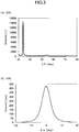
FIG. 3 shows orientations of the stacking of the piezoelectric layer over the orientation control layer of amorphous phase fabricated according to the embodiment; -
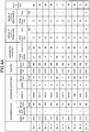
FIG. 4A illustrates experimental results of evaluating properties of piezoelectric sensors according to the embodiment; -
FIG. 4B illustrates experimental results of evaluating properties of piezoelectric sensors according to the embodiment; -
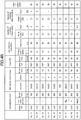
FIG. 4C illustrates experimental results of evaluating properties of piezoelectric sensors according to comparative examples; -
FIG. 5 is a schematic diagram illustrating a response evaluation test for piezoelectric devices fabricated; -
FIG. 6 illustrates an example of measurement acquired from the response evaluation test ofFIG. 5 ; -
FIG. 7 is a schematic diagram of a modification of piezoelectric device; -
FIG. 8 is a schematic diagram of another modification of piezoelectric device; -
FIG. 9 is a schematic diagram of still another modification of piezoelectric device; and -
FIG. 10 is a schematic diagram of still another modification of piezoelectric device. - In general, to enhance the orientation of a wurtzite material, it is considered to be better to dispose a crystal film under the wurtzite material because the wurtzite crystal can grow in alignment with the crystal structure of the underlayer. It is also assumed that a piezoelectric layer using a crystal-orientated wurtzite material is formed sufficiently thick to improve the crystallinity. However, increasing the thickness of the piezoelectric layer tends to cause cracking or crazing, as has been described above. This tendency appears more conspicuously particularly when a flexible plastic layer is used as a substrate. In contrast, according to the present invention, an orientation control layer of amorphous phase is disposed under a piezoelectric layer with a wurtzite crystal structure, thereby reducing the thickness of the piezoelectric layer, suppressing cracking or crazing, and achieving a satisfactory piezoelectric property.
-
FIG. 1 is a schematic diagram of apiezoelectric sensor 10A which is an example of the piezoelectric device. Thepiezoelectric sensor 10A is formed in a layered structure including a pair ofelectrodes plastic layer 12, in which astacking 15 of anorientation control layer 13 and apiezoelectric layer 14 is provided between theelectrodes FIG. 1 , theelectrode 11 serves as a transparent bottom electrode, and theelectrode 19 serves as a transparent top electrode. The transparency of theelectrode 11 and theelectrode 19 is not always required; however, when applied to a display, including a touch panel, it is desirable for thepiezoelectric sensor 10A to have a transparent electrode made of ITO, IZO or the like. - The
piezoelectric layer 14 is made of a piezoelectric material with a wurtzite crystal structure, and has a thickness of 20 nm to 250 nm. With this range of thickness of thepiezoelectric layer 14, cracking and/or crazing can be suppressed. If the thickness of thepiezoelectric layer 14 exceeds 250 nm, cracking or crazing is more likely to occur, which affects the degree of haze. When the thickness of thepiezoelectric layer 14 is less than 20 nm, it is difficult to achieve a satisfactory piezoelectric property (or a polarization property in accordance to pressure) even when theorientation control layer 13 is used as the underlayer. Here, the thickness of thepiezoelectric layer 14 is preferably 30 nm to 200 nm, and more preferably 50 nm to 100 nm. - The wurtzite crystal structure is represented by general formula AB, where A denotes cation (An+) and B denotes anion (Bn-). It is desirable for the wurtzite piezoelectric material to exhibit the piezoelectric effect to a certain extent or more and be crystallized at a low-temperature process of 200°C or below. Examples of such a material include zinc oxide (ZnO), zinc sulfide (ZnS), zinc selenide (ZnSe), zinc telluride (ZnTe), aluminum nitride (AlN), gallium nitride (GaN), cadmium selenide (CdSe), telluride Cadmium (CdTe), silicon carbide (SiC), etc. Any one of these components or a combination of two or more elements used in the above-described components may be used. When using a combination of two or more elements, thin films of the respective elements may be layered. Alternatively, one of or a combination of two or more of these components may be used as the basic component, and other elements may be added optionally as a sub component. The content of the sub component (i.e., element(s) other than the basic component) will not be limited as long as the advantageous effect of the present invention is achieved. The content of element(s) to be added other than the basic component may range from 0.1 at.% to 20 at.%, preferably equal to or greater than 0.1 at.% and equal to or less than 10 at.%, and more preferably equal to or greater than 0.2 at.% and equal to or less than 5 at.%. For example, a wurtzite material whose basic component is ZnO or AlN may be used, and a metal that does not exhibit electrical conductivity when added may be doped in ZnO or AlN. Such a dopant may include, but is not limited to, silicon (Si), magnesium (Mg), vanadium (V), titanium (Ti), zirconium (Zr), etc. One of, or two or more of the dopants may be added. By adding these metals, the frequency of occurrence of cracking or crazing can be reduced, which will be described in more detail below. When a transparent wurtzite crystal material is used as the
piezoelectric layer 14, it is suitable for application to a display. - The
orientation control layer 13 provided under thepiezoelectric layer 14 is an amorphous layer with a thickness of 3 nm to 100 nm. Using theorientation control layer 13 with the film thickness of this range, the crystal orientation (c-axis orientation) of thepiezoelectric layer 14 can be improved. By selecting the film thickness of theorientation control layer 13 of amorphous phase ranging from 3 nm to 100 nm, the full width at half maximum (FWHM) of the X-ray rocking curve with respect to thepiezoelectric layer 14 is maintained low, as will be described later. - The
orientation control layer 13 may be formed of an inorganic material, an organic material, or a mixture of an inorganic material and an organic material. As the inorganic material, silicon oxide (SiOx), silicon nitride (SiN), aluminum nitride (AlN), aluminum oxide (Al2O3), gallium nitride (GaN), gallium oxide (Ga2O3), or the like may be used. ZnO to which Al2O3 and SiOx are added (hereinafter referred to as "SAZO") may also be used. Alternatively, GaN, AlN, or ZnO to which at least one of Al2O3, Ga2O3, SiOx, and SiN is added may be used. Examples of the organic material include, but are not limited to, acrylic resins, urethane resins, melamine resins, alkyd resins, and siloxane polymers. In particular, it is preferable to use a thermosetting resin made of a mixture of a melamine resin, an alkyd resin, and an organic silane condensate as the organic substance. Using the above materials, an amorphous film can be formed by vacuum evaporation, sputtering, ion plating, coating, or the like. The orientation control layer may be a single layer or a multilayer including two or more films. When using a multilayer, an inorganic thin film and an organic thin film may be stacked. - The
orientation control layer 13 formed in amorphous phase using these materials is superior in surface smoothness and it controls the orientation of the c-axis of the wurtzite material of the upper layer to align in the vertical (or the layered) direction. Besides, the gas barrier property is high, and the adverse influence of a gas generated from the plastic layer during the process of deposition of the films can be reduced. In particular, a thermosetting resin is amorphous and its surface is highly smooth. A melamine resin is dense owing to the three-dimensional crosslinked structure, and has a high barrier property. Although the orientation control layer according to the present invention is formed in amorphous phase, the entirety of the orientation control layer is not necessarily amorphous, and a non-amorphous portion may be included as long as the effect of the present invention is achieved. In the orientation control layer, the proportion of the amorphous part is 90% or more, preferably 95% or more, and more preferably 100%. - The
plastic layer 12 is formed of a flexible material capable of imparting flexibility to thepiezoelectric sensor 10A. The thickness of theplastic layer 12 is preferably 5pm to 150 µm, and more preferably 20µm to 125 µm. Materials of theplastic layer 12 includes, but are not limited to, polyethylene terephthalate (PET), polyethylene naphthalate (PEN), polycarbonate (PC), acrylic resin, cycloolefin polymer, polyimide (PI), or the like. Among these materials, polyethylene terephthalate (PET), polyethylene naphthalate (PEN), polycarbonate (PC), acrylic resin, and cycloolefin polymer are colorless, transparent materials, and they are suitable whenelectrodes piezoelectric sensor 10A as in a health care product such as a pulse meter or a heart rate monitor, or in an in-vehicle pressure detection sheet, a semi-transparent or non-transparent plastic material may be used. - Although in the configuration of
FIG. 1 , theplastic layer 12 is provided between theelectrode 11 and the stacking 15, the position of theplastic layer 12 is not limited to this example, and a suitable position may be selected as long as theplastic layer 12 imparts the flexibility to thepiezoelectric sensor 10A. - The
piezoelectric sensor 10A can be fabricated by the following process. Theelectrode 11 is formed over the back face of theplastic layer 12 that serves as a plastic base. Theelectrode 11 is, for example, an ITO film formed by direct current (DC) or radio frequency (RF) magnetron sputtering. Depending on the application of the device, the ITO film may be formed as a full-coverage solid electrode, or it may be processed into a predetermined pattern by etching or the like. When thepiezoelectric sensor 10A is used as a pressure sensor for a touch panel or the like, theelectrode 11 may be patterned into multiple stripes arranged in parallel along a first direction. - An
orientation control layer 13 is formed in amorphous phase over the top face of theplastic layer 12, opposite to theelectrode 11, at a thickness of 3 nm to 100 nm by, for example, sputtering at room temperature. When the thickness is less than 3 nm, it becomes difficult to sufficiently improve the orientation of the upperpiezoelectric layer 14. With the thickness exceeding 100 nm, it also becomes difficult to improve the crystallinity of the upperpiezoelectric layer 14. The temperature for the film formation of theorientation control layer 13 is not necessarily room temperature as long as the amorphous phase can be maintained, and theorientation control layer 13 may be formed at, for example, a substrate temperature of 150°C or below. - Subsequently, the
piezoelectric layer 14 is formed over theorientation control layer 13. For example, a ZnO target is used to form a film by RF magnetron sputtering in a mixed gas atmosphere of argon (Ar) and a small amount of oxygen (O2). The film thickness of theZnO piezoelectric layer 14 is 20 nm to 250 nm. The stacking 15 is formed by theorientation control layer 13 and thepiezoelectric layer 14. The film forming temperature of ZnO is not necessarily a room temperature as long as the amorphous phase of the under layer, that is, theorientation control layer 13 is maintained during the process. Thepiezoelectric layer 14 may be formed at, for example, a substrate temperature of 150°C or below. - When adopting sputtering to form the
orientation control layer 13 and thepiezoelectric layer 14, a uniform file with strong adhesion can be formed while substantially maintaining the composition ratio of the compound of the target. In addition, a film can be formed at a desired thickness highly accurately only by controlling the time. - Then, an
electrode 19 is formed in a predetermined pattern over thepiezoelectric layer 14. For theelectrode 19, an ITO film with a thickness of 20 nm to 100 nm may be formed by DC or RF magnetron sputtering at room temperature. Theelectrode 19 may be a full-coverage solid layer formed over the entire surface of the layered structure. Alternatively, when thebottom electrode 11 is patterned into parallel stripes, theelectrode 19 may also be patterned into stripes extending in a direction orthogonal to the stripes of the bottom electrode. Thus, thepiezoelectric sensor 10A is fabricated. - After the
electrode 19 is formed, the entirety of thepiezoelectric sensor 10A may be heat-treated at a temperature (for example, 130°C) lower than the melting point or the glass transition point of theplastic layer 12. By this post-heating, the ITO electrode can be crystallized to reduce the electrical resistance. This heat treatment is not indispensable, and it may not be performed because thepiezoelectric layer 14 has a satisfactory degree of crystal orientation owing to the amorphous-phaseorientation control layer 13 positioned below so as to sufficiently exhibit the piezoelectric response even without the post-heating. Depending on the material of theplastic layer 12, theplastic layer 12 may not be thermostable or heat-resistant, and it may be desirable not to perform post-heating depending on the situation. The stacking 15 of theorientation control layer 13 of amorphous phase and thepiezoelectric layer 14 formed thereon is particularly advantageous when aplastic layer 12 with low heat resistance is used to ensure flexibility. -
FIG. 2 shows cross-sectional TEM images of the stacking of theorientation control layer 13 and thepiezoelectric layer 14 actually fabricated over a plastic (PET)base film 20.FIG. 2 (A) is an enlarged view at magnifications of 500,000 times, andFIG. 2 (B) is an enlarged view at magnifications of 2 million times. Amorphous SAZO is used as theorientation control layer 13 and zinc oxide (ZnO) is used as thepiezoelectric layer 14. In general, "AZO" comprised of ZnO as the basic component with Al2O3 added as a sub component is a conductive film with high crystallinity. By further adding SiO2, an amorphous and electrically insulating SAZO film can be obtained. The thickness of thisorientation control layer 13 is 10 nm, and the thickness of thepiezoelectric layer 14 is 50 nm. As can be observed from the TEM image ofFIG. 2 (A) , thepiezoelectric layer 14 is formed over the amorphousorientation control layer 13 having a smooth and uniform surface. In the TEM image ofFIG. 2 (B) , a large number of lines running in the vertical direction of thepiezoelectric layer 14 indicate the direction of crystal growth. It is clearly shown that the c-axis of thepiezoelectric layer 14 is aligned vertical to the substrate. -
FIG. 3 shows X-ray measurement results of the sample ofFIG. 2 .FIG. 3 (A) shows an X-ray diffraction (XRD) pattern obtained by θ-2θ measurement, andFIG. 3 (B) shows an X-ray rocking curve across (0002) reflection from the ZnO. The vertical axis ofFIG. 3 (A) represents intensity (as an arbitrary unit), and the vertical axis ofFIG. 3 (B) represents intensity as the number of counts per second [cps]. InFIG. 3 (A) , a strong peak derived from the (002) facet of ZnO appears at a diffraction angle (2θ) of 34° (degrees). The small peaks observed in the vicinity of 54° and 72° in terms of 2θ are derived from the PET base material. Theorientation control layer 13 is made of amorphous SAZO and crystal growth is hardly observed in the cross-sectional TEM image ofFIG. 2 (B) , unlike theZnO piezoelectric layer 14. - In the rocking curve measurement, a wafer (that is, a crystal surface) is rotated, while the X-ray source and the detector are fixed, to acquire a tilt distribution of crystal axes, and fluctuations in crystal orientation in the thin film are observed. The FWHM value of the rocking curve of
FIG. 3 (B) is indicative of the c-axis orientation of thepiezoelectric layer 14. The smaller the FWHM value, the better the crystal orientation. In this sample, the FWHM (representing the c-axis orientation) is satisfactory as 14°. A preferred range of the FWHM value indicative of the c-axis orientation is 3° to 15°. - 4A and 4B show evaluation results of samples of Examples 1 to 19, which are fabricated by varying parameters of the stacking 15 and with different materials of the base film.
FIG. 4C shows evaluation results of samples withcomparative structures 1 to 10 in the table. The parameters of the sample include material, thickness, and subcomponent(s) (additives) of thepiezoelectric layer 14; material, phase (amorphous or crystalline), and thickness of theorientation control layer 13; and material and thickness of the base film. Items to be evaluated include c-axis orientation and piezoelectric response as for piezoelectric properties, and visual inspection and haze measurement (cloudy appearance) as for degree of cracking. The degree of cracking is observed both in the initial state and after bending test. - The c-axis orientation is judged from measurement of X-ray rocking curve on each sample and by determining the FWHM value. Piezoelectric response is judged from measurement of a voltage level generated under application of a pressure onto the sample. Satisfactory piezoelectric response is indicated by a double circle (⊚), acceptable piezoelectric response is indicated by a single circle (○), and poor piezoelectric response is indicated by a cross mark (x).
- The degree of cracking is an index used to judge whether cracks exist or not and to what extent cracks occur. For the evaluation of the degree of cracking, two types of assessments, visual inspection and haze measurement, are performed. Visual inspection is assessment of the sample appearance. When no cloudiness or unclearness is observed at a first glance, it is assessed as acceptable and marked with a single circle. When any cloudiness or unclearness is observed at a first glance, it is assessed as unacceptable (marked with "x"). The haze is indicated by a haze value (%) of the sample measure by a haze meter manufactured by Suga Test Instruments Co., Ltd. The degree of cracking (after bending) is judged by visual inspection and haze measurement after the sample is placed around a cylinder with a diameter of 9 mm and held for 30 seconds under a load of 100 grams.
- The criteria for the overall evaluation are as follows:
- Good (marked with double circle "⊚"): Piezoelectric properties are good (with double circle), and degree of cracking is acceptable with acceptable visual inspection result (with single circle) and a haze value less than or equal to 5.0 for those samples to which haze measurement is performed:
- Acceptable (marked with single circle "○"): piezoelectric properties are acceptable (with single circle), and degree of cracking is acceptable with acceptable visual inspection result (with single circle) and a haze value less than or equal to 5.0 for those samples to which haze measurement is performed:
- Unacceptable (marked with "x"): Piezoelectric properties do not meet the required conditions, or the degree of cracking is unacceptable (marked with "x") with cloudiness or cracking observed by visual inspection and a haze value of more than 5.0 for those samples to which haze measurement is performed.
- As the plastic base film, cyclo-olefin polymer (COP) with a thickness of 100 µm is used. On the COP is a 10 nm thick SAZO amorphous film formed as the
orientation control layer 13 by DC magnetron sputtering at room temperature. Theorientation control layer 13 was formed in a mixed gas of argon (Ar) and oxygen (O2), under a process pressure of 0.2 Pa, using a 4-inch flat target, and at an output power of 200 W. Over the SAZO amorphous film, a 50 nm thick ZnO film is formed as thepiezoelectric layer 14 by RF magnetron sputtering at room temperature. Thepiezoelectric layer 14 was formed in an Ar/O2 mixed gas under a process pressure of 0.2 Pa, using a 4-inch flat target, and at an output power of 300 W. - A sample of 3 mm diameter (or 3 mm × 3 mm square) is fabricated by the above-described process. As a parameter for the piezoelectric property, the c-axis orientation of this sample was evaluated by X-ray rocking curve measurement. A good FWHM value of 11° was obtained. In addition, as a direct evaluation index of piezoelectric property, a piezoelectric response was evaluated under the application of a pressure. The piezoelectric response is measured by setting the fabricated sample in an experimental setup illustrated in
FIG. 5 and reading a voltage. - In
FIG. 5 , a sample with the stacking 15 formed on thebase film 20 is sandwiched between a pair ofelectrodes piezoelectric device 10. Thepiezoelectric device 10 is fixed onto thestage 30 with anadhesive layer 31. The layered structure of thispiezoelectric device 10 is the same as that of thepiezoelectric sensor 10A illustrated inFIG. 1 . An external pressure is applied to thepiezoelectric device 10 and a voltage between theelectrodes -
FIG. 6 shows the measured piezoelectric response. Voltage peaks are observed at regular intervals with very little time lags from the pressure application point of time, and there is little variation in peak values. The piezoelectric response of this sample is judged to be good (marked with double circle). - Then, the degree of cracking is judged from the appearance of the sample. At a first glance of the sample, no cloudiness (or cracks) is observed, and the degree of cracking is evaluated as acceptable (marked with single circle). Then, for post-bending evaluation, the sample was wound around a cylinder with a diameter of 9 mm, and bending stress is applied with a load of 100 grams to observe occurrence of cracking or crazing. Even after the bending test, cracking is not observed and the sample is evaluated as acceptable (marked with single circle). The overall evaluation of the sample of Example 1 is good (marked with double circle).
- A 10 nm thick SAZO amorphous film is formed as the
orientation control layer 13 over a 100 µm thick COP at room temperature. Over the SAZO amorphous film is a 30 nm thick ZnO film formed as thepiezoelectric layer 14 at room temperature, and a sample of 3 mm diameter (or 3 mm × 3 mm square) is fabricated. The film forming conditions of the respective layers are the same as those in Example 1, except for the deposition time of thepiezoelectric layer 14. In the sample of Example 2, the thickness of thepiezoelectric layer 14 is reduced as compared with Example 1. The FWHM value representing the c-axis orientation of this sample is 14° which is slightly greater than that of Example 1 because of the decrease in the film thickness of the piezoelectric layer, and piezoelectric response is not as high as Example 1; however, these parameters are in the satisfactory range. Because thepiezoelectric layer 14 is made thinner, it is strong with respect to cracking or crazing and exhibits good flexibility. No cloudiness or cracks have been observed in the visual inspection for the evaluation of degree of cracking. The overall evaluation of this sample is acceptable (marked with single circle) . - A 10 nm thick SAZO amorphous film is formed as the
orientation control layer 13 over a 100 µm thick COP at room temperature. Over the SAZO amorphous film is a 100 nm thick ZnO film formed as thepiezoelectric layer 14 at room temperature, and a sample of 3 mm diameter (or 3 mm × 3 mm square) is fabricated. The film forming conditions of the respective layers are the same as those in Example 1, except for the deposition time of thepiezoelectric layer 14. In the sample of Example 3, the thickness of thepiezoelectric layer 14 is doubled as compared with Example 1. The FWHM value representing the c-axis orientation of this sample is as small as 9° because of the increased thickness of thepiezoelectric layer 14, and high piezoelectric response is obtained. Meanwhile, the flexibility is not so high as Examples 1 and 2, but is still in the acceptable range. In the visual inspection for the evaluation of degree of cracking, no cloudiness or cracks are observed. The overall evaluation of this sample is good (marked with double circle). - A 10 nm thick SAZO amorphous film is formed as the
orientation control layer 13 over a 100 µm thick COP at room temperature. Over the SAZO amorphous film is a 200 nm thick ZnO film formed as thepiezoelectric layer 14 at room temperature, and a sample of 3 mm diameter (or 3 mm × 3 mm square) is fabricated. The film forming conditions of the respective layers are the same as those in Example 1, except for the deposition time of thepiezoelectric layer 14. In the sample of Example 4, the thickness of thepiezoelectric layer 14 is further increased compared with Example 3. The FWHM value representing the c-axis orientation of this sample is as small as 7° because of the increased thickness of thepiezoelectric layer 14, and high piezoelectric response is obtained. On the other hand, the flexibility is not so high as Examples 1 and 2, but is still in the acceptable range. In the visual inspection for the evaluation of degree of cracking, no cloudiness or cracks are observed. The overall evaluation of this sample is good (marked with double circle). - A 50 nm thick SAZO amorphous film is formed as the
orientation control layer 13 over a 100 µm thick COP at room temperature. Over the SAZO amorphous film is a 50 nm thick ZnO film formed as thepiezoelectric layer 14 at room temperature, and a sample of 3 mm diameter (or 3 mm × 3 mm square) is fabricated. The film forming conditions of the respective layers are the same as those in Example 1, except for the deposition time of theorientation control layer 13. In the sample of Example 5, the thickness of thepiezoelectric layer 14 is as thin as that of Example 1, and thepiezoelectric layer 14 and theorientation control layer 13 have the same thickness. The FWHM value representing the c-axis orientation of this sample is 15° which is slightly greater that those of Examples 1 to 4, but both the c-axis orientation and the piezoelectric response are sufficiently acceptable. The flexibility is not so high as Examples 1 and 2 due to the slightly increased total thickness of the stacking 15 including theorientation control layer 13 and thepiezoelectric layer 14, but it is sufficiently acceptable. In the visual inspection for the evaluation of degree of cracking, no cloudiness or cracks are observed. The overall evaluation of this sample is acceptable (marked with single circle). - A SAZO amorphous film of 3 nm thickness is formed as the
orientation control layer 13 over a 100 µm thick COP at room temperature. Over the SAZO amorphous film is a 50 nm thick ZnO film formed as thepiezoelectric layer 14 at room temperature, and a sample of 3 mm diameter (or 3 mm × 3 mm square) is fabricated. The film forming conditions of the respective layers are the same as those in Example 1, except for the deposition time of theorientation control layer 13. In the sample of Example 6, the thickness of thepiezoelectric layer 14 is as thin as that of Example 1, and theorientation control layer 13 is as thin as 3 nm. The FWHM value representing the c-axis orientation of this sample is 15° which is slightly greater that those of Examples 1 to 4, but both the c-axis orientation and the piezoelectric response are sufficiently acceptable. The flexibility is satisfactory because the total thickness of the stacking 15 including theorientation control layer 13 and thepiezoelectric layer 14 is small. In the visual inspection for the evaluation of degree of cracking, no cloudiness or cracks are observed. The overall evaluation of this sample is acceptable (marked with single circle). - A 10 nm thick SAZO amorphous film is formed as the
orientation control layer 13 over a 50 µm thick polyimide (PI) film at room temperature. Over the SAZO amorphous film is a 50 nm thick ZnO film formed as thepiezoelectric layer 14 at room temperature, and a sample of 3 mm diameter (or 3 mm × 3 mm square) is fabricated. The film forming conditions of the respective layers are the same as those in Example 1. In the sample of Example 8, the material and the thickness of the plastic base film are different from those in Example 1 and 7, but the material and the thickness of theorientation control layer 13 and thepiezoelectric layer 14 are the same as those in Example 1 and 7. The FWHM value representing the c-axis orientation of this sample is 11° which is the same as that in Example 1 and 7, and both the c-axis orientation and the piezoelectric response are good. The flexibility is also as good as Example 1. In the visual inspection for the evaluation of degree of cracking, no cloudiness or cracks are observed. The overall evaluation of this sample is good (marked with double circle). - An amorphous aluminum nitride (AlN) film of a thickness of 50 nm is formed as the
orientation control layer 13 on a 100 µm thick COP film by RF magnetron sputtering at room temperature. Theorientation control layer 13 is formed in an Ar/O2 mixed gas under a process pressure of 0.2 Pa, using a 4-inch flat target, and at an output power of 200 W. Over the AlN amorphous film is a 50 nm thick ZnO film formed as thepiezoelectric layer 14 at room temperature, and a sample of 3 mm diameter (or 3 mm × 3 mm square) is fabricated. The film forming conditions of thepiezoelectric layer 14 are the same as those in Example 1. In the sample of Example 9, the material and the thickness of the amorphous-phaseorientation control layer 13 are different from those in Example 1. The FWHM value representing the c-axis orientation of this sample is 14° which is slightly greater than that in Example 1, but both the c-axis orientation and the piezoelectric response are in the satisfactory range. The flexibility is good with no cracking observed. In the visual inspection for the evaluation of degree of cracking, no cloudiness or cracks are observed. The overall evaluation of this sample is good (marked with double circle). - An amorphous silicon dioxide (SiO2) film of a thickness of 50 nm is formed as the
orientation control layer 13 on a 100 µm thick COP film by RF magnetron sputtering at room temperature. Theorientation control layer 13 is formed in an Ar/O2 mixed gas under a process pressure of 0.2 Pa, using a 4-inch flat target, and at an output power of 200 W. Over the SiO2 amorphous film is a 50 nm thick ZnO film formed as thepiezoelectric layer 14 at room temperature, and a sample of 3 mm diameter (or 3 mm × 3 mm square) is fabricated. The film forming conditions of thepiezoelectric layer 14 are the same as those in Example 1. In the sample of Example 10, the material and the thickness of the amorphous-phaseorientation control layer 13 are different from those in Example 1 and 9. The FWHM value representing the c-axis orientation of this sample is 15° which is slightly greater than that in Example 1, but both the c-axis orientation and the piezoelectric response are within the acceptable range. In the visual inspection for the evaluation of degree of cracking, no cloudiness or cracks are observed. The overall evaluation of this sample is acceptable (marked with single circle). - An amorphous SAZO film of a thickness of 10 nm is formed on a 125 µm thick PET base film. Over the SAZO amorphous film is a 50 nm thick ZnO film formed as the
piezoelectric layer 14 at room temperature, and a sample of 3 mm diameter (or 3 mm × 3 mm square) is fabricated. The sample is wound around a cylinder with a diameter of 9 mm and held for 30 seconds with a load of 100 grams, and then haze measurement is performed. Further, the c-axis orientation and the piezoelectric response are evaluated after the haze test. In the visual evaluation, no cloudiness is observed and the transparency of the sample is maintained even after the haze evaluation. The haze value is as small as "2". The FWHM value representing the c-axis orientation of this sample is 14° which is satisfactory, and both the c-axis orientation and the piezoelectric response are good. The overall evaluation of this sample is good (marked with double circles). - A sample in which the thickness of the ZnO film serving as the piezoelectric layer is changed to 100 nm, while the other conditions are the same as those in Example 10, is fabricated, and haze measurement is performed in addition to the visual inspection as in Example 10. The transparency of the sample is maintained even after the haze measurement. The c-axis orientation is as small as 12°, and the piezoelectric response is good (with double circle). The overall evaluation of this sample is good (marked with double circles).
- A sample in which the thickness of the ZnO film serving as the piezoelectric layer is changed to 200 nm, while the other conditions are the same as those in Example 11, is fabricated, and haze measurement was performed in addition to the visual inspection as in Example 10. The transparency of the sample is maintained even after the haze measurement, and the haze value is 5%, which is within the acceptable range. The FWHM representing the c-axis orientation is as small as 9°, and the piezoelectric response is good (with double circle). The overall evaluation of this sample is good (marked with double circles).
- The thickness of the ZnO film that serves as the piezoelectric layer is set to 200 nm as in Example 12, and the thickness of the PET film used as the plastic base film is changed to 50 µm. The other conditions are the same as those in Example 12. The FWHM representing the c-axis orientation is 14° which is within the satisfactory range, and the piezoelectric response is good (with double circle). In the visual inspection for evaluating the degree of cracking, no cloudiness is observed and the haze value is "5" which is within the acceptable range. The overall evaluation of this sample is good (marked with double circles).
- The thickness of the ZnO film that serves as the piezoelectric layer is set to 200 nm as in Example 12, and the thickness of the PET film used as the plastic base film is changed to 38 µm. The other conditions are the same as those in Example 12. The FWHM representing the c-axis orientation is as small as 11°, and the piezoelectric response is also good (with double circle). In the visual inspection for evaluating the degree of cracking, no cloudiness is observed. The overall evaluation of this sample is good (marked with double circles).
- The thickness of the ZnO film that serves as the piezoelectric layer is set to 200 nm as in Example 12, and the thickness of the PET film used as the plastic base film is changed to 25 µm. The other conditions are the same as those in Example 12. The FWHM representing the c-axis orientation is as small as 13°, and both the c-axis orientation and the piezoelectric response are good (with double circle). In the visual inspection for evaluating the degree of cracking, no cloudiness is observed. The overall evaluation of this sample is good (marked with double circles).
- An
orientation control layer 13 is formed with an amorphous thermosetting resin at a thickness of 50 nm on a PET film of 50 µm thickness. For the material of theorientation control layer 13, a thermosetting resin composition that contains a melamine resin, an alkyd resin, and an organic silane condensate at a weight ratio of 2 to 2 to 1 (2:1*1) as a solid content is diluted with methyl ethyl ketone such that the solid content concentration becomes 8 wt%. This solution is applied onto a main surface of the PET film and cured by heating at 150 °C for 2 minutes to form theorientation control layer 13 with a film thickness of 50 nm and a refractive index of 1.54. Over the amorphous-phaseorientation control layer 13 is a 200 nm thick ZnO film formed as thepiezoelectric layer 14 at room temperature, and a sample of 3 mm diameter (or 3 mm × 3 mm square) is fabricated. The film forming conditions of thepiezoelectric layer 14 are the same as those in Example 1, except for the deposition time. In the sample of Example 16, the material and the thickness of theorientation control layer 13 are different from Example 1. The FWHM value representing the c-axis orientation of this sample is 14° which is slightly greater than that of Example 1; however both the c-axis orientation and the piezoelectric response are in the satisfactory range. Flexibility is also good without visible cloudiness or cracks observed by the visual inspection for the evaluation of the degree of cracking. The overall evaluation of the sample is good (marked with double circle). - An amorphous-phase
orientation control layer 13 of a thickness of 50 nm is formed using an inorganic material SAZO on a PET film of 50 µm thickness. Over the amorphous-phaseorientation control layer 13 is apiezoelectric layer 14 formed at a thickness of 200 nm. Thispiezoelectric layer 200 is a ZnO film that contains a 10 wt% magnesium (Mg) added as a dopant. With this composition, a sample of 3 mm diameter (or 3 mm × 3 mm square) is fabricated. The FWHM value representing the c-axis orientation of the sample of Example 17 is as small as 11°, and the piezoelectric response is also good. As to the flexibility, no cloudiness or cracks are observed in the visual inspection before and after the haze measurement, and evaluation is within the acceptable range. The haze value is as small as 1%. The overall evaluation of this sample is good (marked with double circle). It is understood that by adding Mg in thepiezoelectric layer 14, the crack suppressing effect is improved. - An amorphous-phase
orientation control layer 13 of a thickness of 50 nm is formed using an inorganic material SAZO on a PET film of 50 µm thickness. Over the amorphous-phaseorientation control layer 13 is apiezoelectric layer 14 formed at a thickness of 200 nm. Thispiezoelectric layer 200 is a ZnO film that contains a 2 wt% vanadium (V) added as an dopant. With this composition, a sample of 3 mm diameter (or 3 mm × 3 mm square) is fabricated. The FWHM value representing the c-axis orientation of the sample of Example 18 is as small as 10°, and the piezoelectric response is also good. As to the flexibility, no cloudiness or cracks are observed in the visual inspection before and after the haze measurement, and evaluation is within the acceptable range. The overall evaluation of this sample is good (marked with double circle). It is understood that by adding V in thepiezoelectric layer 14, the crack suppressing effect is acquired as in Example 17. - An amorphous-phase
orientation control layer 13 of a thickness of 50 nm is formed using an inorganic material SAZO on a PET film of 50 µm thickness. Over the amorphous-phaseorientation control layer 13 is apiezoelectric layer 14 formed at a thickness of 200 nm. Thispiezoelectric layer 200 is a ZnO film that contains a 10 wt% magnesium (Mg) and 2 wt% silicon (Si) both added as dopants. With this composition, a sample of 3 mm diameter (or 3 mm × 3 mm square) is fabricated. The FWHM value representing the c-axis orientation of the sample of Example 18 is as small as 10°, and the piezoelectric response is also good. As to the flexibility, no cloudiness or cracks are observed in the visual inspection before and after the haze measurement, and evaluation is within the acceptable range. The haze value is 0.7 which is smaller than that in Example 17. The overall evaluation of this sample is good (marked with double circle). It is understood that by adding Mg and Si in thepiezoelectric layer 14, the crack suppressing effect is improved. - For
Comparative Case 1, a sample that does not use an orientation control layer as the underlayer is fabricated. A ZnO film with a thickness of 50 nm is formed as thepiezoelectric layer 14 at room temperature directly on a COP film with a thickness of 100 µm, and a sample of 3 mm diameter (or 3 mm × 3 mm square) is fabricated. The film forming conditions of thepiezoelectric layer 14 are the same as those in Example 1. Since the sample ofComparative Case 1 does not have an orientation control layer under the piezoelectric layer, the FWHM value representing the c-axis orientation is as great as 27°, and the piezoelectric response is out of the acceptable range. In the visual inspection for evaluating the degree of cracking, no cloudiness or the like is observed. The overall evaluation of this sample is "unacceptable" (marked with "x"). - For
Comparative Case 2, a crystal-phase orientation control layer is inserted as the underlayer of thepiezoelectric layer 14.
A crystal-phase ITO film with a thickness of 30 nm is formed as theorientation control layer 13 on the COP film of a 100 µm thickness by DC magnetron sputtering. The film forming conditions for theorientation control layer 13 are using the Ar/oxygen mixed gas and a 4-inch flat target, at a process pressure of 0.2 Pa and the output power of 200 W. In order for crystallization of ITO, the substrate temperature is set to approximately 150 °C during the sputtering process. Then, a ZnO film with a thickness of 50 nm is formed as apiezoelectric layer 14 on the ITO film at room temperature, and a sample with a diameter of 3 mm (or 3 mm × 3 mm square). The film forming conditions for thepiezoelectric layer 14 are the same as those in Example 1. The ITO film ofComparative Case 2 serves both as an orientation control layer and a bottom electrode. The FWHM value representing the c-axis orientation of this sample is as great as 26°, and the piezoelectric response is out of the acceptable range. Although no cloudiness or the like is observed in the visual inspection for evaluating the degree of cracking, the overall evaluation is "unacceptable" (marked with "x") due to insufficient piezoelectric properties. - In
Comparative Case 3, the conditions are the same as in Example 1 except for the thickness of thepiezoelectric layer 14. An amorphous-phase SAZO film of a 10 nm thickness is formed as anorientation control layer 13 on a COP film with a thickness of 100µm at room temperature. On the amorphous-phase SAZO film is a ZnO film with a thickness of 400 nm formed as apiezoelectric layer 14 at room temperature, and a sample of a diameter of 3 mm (or 3 mm × 3 mm square) is fabricated. The film forming conditions of thepiezoelectric layer 14 are the same as those in Example 1 except for the deposition time. The sample ofComparative Case 3 has good crystallinity because the thickness of thepiezoelectric layer 14 is increased. The FWHM value representing the c-axis orientation is as small as 7°, and high piezoelectric response is achieved. However, since thepiezoelectric layer 14 is as thick as 400 nm, many cracks are observed by visual inspection for evaluating the degree of cracking, and cloudiness is observed in the sample. Due to the large number of cracks, the reliability of operation is impaired. The overall evaluation of this sample is "unacceptable" (marked with "x"). - In
Comparative Cases 4 to 8, PET with a thickness of 125 µm is used as the plastic base film, and the thickness of the ZnO film used as the piezoelectric layer is varied to 50 nm, 100 nm, 200 nm, 400 nm, and 800 nm, without providing the orientation control layer. InComparative Cases 4 to 6, the haze value is maintained at a low value both in the initial state and after the bending test, and no clouding is observed by visual inspection (marked with single circle). However, the FWHM value representing the c-axis orientation is large, and the piezoelectric response is out of the acceptable range (marked with "x"). InComparative Cases Comparative Cases 4 to 8 are "unacceptable" (marked with "x"). - In
Comparative Cases Comparative Case 9 with the ZnO film of the 400 nm thickness, the FWHM value representing the c-axis orientation is relatively small and the piezoelectric response is in the acceptable range. However, since the thickness of the ZnO film is increased, cracks are observed by the visual inspection for evaluating the degree of cracking, and the haze value becomes high. The evaluation of the degree of cracking is out of the acceptable range (marked with "x"). InComparative Case 10 with the ZnO film with a thickness of 800 nm, the FWHM value representing the c-axis orientation is small and good piezoelectric response is achieved. However, the haze value (in the initial state) is further increased, compared withComparative Case 9. In the visual inspection, cracks are observed and the evaluation is out of the acceptable range (marked with "x"). The overall evaluations ofComparative Cases - From the results of Examples 1 to 15 and
Comparative Cases 1 to 8, the advantageous effect of using the amorphous-phaseorientation control layer 13 as the underlayer of thepiezoelectric layer 14 is recognized; that is, satisfactory piezoelectric properties and flexibility (or crack suppression) are both achieved. - From the results of Examples 1 to 15, it is also understood that amorphous SAZO, AlN, or SiOx film is used favorably as the
orientation control layer 13. In addition to these materials, amorphous silicon nitride (SiN), amorphous silicon carbide (SiC), amorphous aluminum oxide (Al2O3), amorphous gallium nitride (GaN), amorphous gallium oxide (Ga2O3), etc. can also be used for theorientation control layer 13. - From the results of Examples 10 to 12 and
Comparative Cases 9 to 10, it is understood that the c-axis orientation and the piezoelectric response can be improved by increasing the thickness of the piezoelectric layer, but the haze value becomes high when the thickness of thepiezoelectric layer 14 is 400 nm or more. In order to achieve both improved piezoelectric properties and crack suppression effect, it is desirable that the thickness of thepiezoelectric layer 14 is in the range of 20 nm to 250 nm. - For the plastic base film, suitable types of polymers or synthetic resins can be used. The thickness of the plastic film capable of imparting flexibility to the
piezoelectric layer 14, without hindering reduction in device thickness, is 5 µm to 150 µm, and more preferably, 25 µm to 125 µm. -
FIG. 7 illustrates a configuration of apiezoelectric sensor 10B which is a modification ofFIG. 1 . In thepiezoelectric sensor 10B, aplastic layer 18 is also disposed on thetop electrode 19. As inFIG. 1 , the stacking 15 of theorientation control layer 13 and thepiezoelectric layer 14 is provided between theelectrode 11 and theelectrode 19. Theelectrode 11 is a transparent electrode that serves as a bottom electrode, and theelectrode 19 is a transparent electrode that serves as an upper electrode. Theorientation control layer 13 is an amorphous thin film with a thickness of 3 nm to 100 nm. Thepiezoelectric layer 14 is made of a wurtzite type piezoelectric material and has a thickness of 20 nm to 250 nm. - The
piezoelectric sensor 10B can be fabricated as follows. Theelectrode 11 is formed on the back surface of theplastic layer 12 which serves as a plastic base film. On the other surface of theplastic layer 12 opposite to theelectrode 11, an amorphous-phaseorientation control layer 13 is formed at a thickness of 3 nm to 100 nm by, for example, sputtering at room temperature. Then, thepiezoelectric layer 14 is formed successively on theorientation control layer 13, whereby the first part of the device is fabricated. - On the other hand, the
electrode 19 is formed in a predetermined shape on theplastic layer 18 which is used as another base film to produce a second part of the device. The material of the first-part plastic layer 12 and the second-part plastic layer 18 may be the same or different from each other. For example, both the first-part plastic layer 12 and the second-part plastic layer 18 may be made of a polymer with a high dielectric constant. Alternatively, the first-part plastic layer 12 may be formed of a material with a higher dielectric constant than that of the second-part plastic layer 18. Thepiezoelectric layer 14 of the first part and theelectrode 19 of the second part are held facing each other and bonded together by anadhesive layer 17. - The
piezoelectric sensor 10B has the amorphous-phaseorientation control layer 13 and thepiezoelectric layer 14 with an appropriate thickness, like thepiezoelectric sensor 10A, and has satisfactory piezoelectric properties. Besides, the plastic layers 12 and 18 are provided under and over the stacking 15, and the device is superior in flexibility. -
FIG. 8 illustrates a configuration of a piezoelectric sensor 10C, which is another modification ofFIG. 1 . In the piezoelectric sensor 10C,plastic layers electrodes orientation control layer 13 and thepiezoelectric layer 14 is provided between theelectrode 11 and theelectrode 19 as inFIG. 1 . Theelectrode 11 is a transparent electrode that serves as a bottom electrode, and theplastic layer 12 is provided between theelectrode 11 and theorientation control layer 13. Theelectrode 19 is a transparent electrode that serves as a top electrode, and theplastic layer 18 is provided between theelectrode 19 and thepiezoelectric layer 14. Theorientation control layer 13 is an amorphous thin film with a thickness of 3 nm to 100 nm. Thepiezoelectric layer 14 is made of a wurtzite type piezoelectric material and has a thickness of 20 nm to 250 nm. - The piezoelectric sensor 10C is fabricated as follows. The
electrode 11 is formed on the back surface of theplastic layer 12 that serves as a plastic base film. An amorphous-phaseorientation control layer 13 and a crystal-phase piezoelectric layer 14 are formed successively on the other surface of theplastic layer 12 opposite to theelectrode 11 to produce a first part. - On the other hand, the
electrode 19 is formed in a predetermined shape on theplastic layer 18 which serves as another plastic base, and a second part is fabricated. The material of the first-part plastic layer 12 and the second-part plastic layer 18 may be the same or different from each other. For example, both theplastic layer 12 of the first part and theplastic layer 18 of the second part may be formed of a polymer with a high dielectric constant. Thepiezoelectric layer 14 of the first part and theplastic layer 18 of the second part are held facing each other, and bonded together by anadhesive layer 17. - The piezoelectric sensor 10C has the amorphous-phase
orientation control layer 13 and thepiezoelectric layer 14 with an appropriate thickness, like thepiezoelectric sensor 10A, and has satisfactory piezoelectric properties. Besides, the plastic layers 12 and 18 are provided under and over the stacking 15, and the device is superior in flexibility. -
FIG. 9 illustrates a configuration of apiezoelectric sensor 10D which is still another modification ofFIG. 1 . In thepiezoelectric sensor 10D, theplastic layer 12 is provided under theelectrode 11, and theplastic layer 18 is provided under theother electrode 19. The stacking 15 of theorientation control layer 13 and thepiezoelectric layer 14 is provided between theelectrode 11 and theelectrode 19 as inFIG. 1 . Theelectrode 11 is a transparent electrode that serves as a bottom electrode, and theelectrode 19 is a transparent electrode that serves as a top electrode. Theorientation control layer 13 is an amorphous thin film and has a thickness of 3 nm to 100 nm. Thepiezoelectric layer 14 is made of a wurtzite type piezoelectric material and has a thickness of 20 nm to 250 nm. - The
piezoelectric sensor 10D is fabricated as follows. Theelectrode 11 is formed in a predetermined shape on theplastic layer 12 serving as a base film. Over theplastic layer 12 with theelectrode 11 having been formed, theorientation control layer 13 and thepiezoelectric layer 14 are formed successively so as to cover theelectrode 11 to produce a first part. On the other hand, theelectrode 19 is formed in a predetermined shape on theplastic layer 18 which is another base film, to produce a second part. The material of the first-part plastic layer 12 and the second-part plastic layer 18 may be the same or different from each other. For example, both the first-part plastic layer 12 and the second-part plastic layer 18 may be formed of a polymer with a high dielectric constant. Alternatively, the first-part plastic layer 12 may be formed of a material having a higher dielectric constant than that of the second-part plastic layer 18. Thepiezoelectric layer 14 of the first part and theplastic layer 18 of the second part are held facing each other and bonded together by anadhesive layer 17. - The
piezoelectric sensor 10D has the amorphous-phaseorientation control layer 13 and thepiezoelectric layer 14 with an appropriate thickness, like thepiezoelectric sensor 10A, and has satisfactory piezoelectric properties. Besides, the plastic layers 12 and 18 are provided under and over the stacking 15, and the device is superior in flexibility.
FIG. 10 illustrates a configuration of apiezoelectric sensor 10E which is still another modification ofFIG. 1 . In thepiezoelectric sensor 10E,plastic layers electrodes orientation control layer 13 and thepiezoelectric layer 14 is provided between theelectrode 11 and theelectrode 19 as inFIG. 1 . Theelectrode 11 is a transparent electrode that serves as a bottom electrode, and theplastic layer 12 is provided under theelectrode 11. Theelectrode 19 is a transparent electrode that serves as a top electrode, and theplastic layer 18 is provided over theelectrode 19. Theorientation control layer 13 is an amorphous thin film with a thickness of 3 nm to 100 nm. Thepiezoelectric layer 14 is made of a wurtzite type piezoelectric material and has a thickness of 20 nm to 250 nm. - The
piezoelectric sensor 10E is fabricated as follows. Theelectrode 11 is formed in a predetermined shape on theplastic layer 12 that serves as a base film. Over theplastic layer 12 with theelectrode 11 having been formed in the predetermined pattern, theorientation control layer 13 and thepiezoelectric layer 14 are formed successively so as to cover theelectrode 11 to produce a first part. On the other hand, theelectrode 19 is formed in a predetermined shape on theplastic layer 18 which serves as another base film to produce a second part. The material of the first-part plastic layer 12 and the second-part plastic layer 18 may be the same or different from each other. Thepiezoelectric layer 14 of the first part and theelectrode 19 of the second part are held facing each other and bonded together by anadhesive layer 17. - The
piezoelectric sensor 10E has the amorphous-phaseorientation control layer 13 and thepiezoelectric layer 14 of an appropriate thickness, like thepiezoelectric sensor 10A, and has satisfactory piezoelectric properties. Besides, the plastic layers 12 and 18 are provided under and over the stacking 15, and the device is superior in flexibility. - In any of the configurations of
FIG. 7 to FIG. 10 , the upper piezoelectric layer has superior c-axis orientation by providing the amorphous-phaseorientation control layer 13 underneath, and it exhibits satisfactory piezoelectric properties. - The configurations of the present invention including the stacking 15 of the amorphous-phase
orientation control layer 13 and the crystal-phase piezoelectric layer 14 can be applied not only to the piezoelectric sensors, but also to other piezoelectric devices such as speakers or oscillators using the inverse piezoelectric effect. Upon application of alternating electrical signals to thepiezoelectric layer 14, mechanical vibrations corresponding to the resonance frequencies are generated in thepiezoelectric layer 14. Owing to the presence of the amorphous-phaseorientation control layer 13 provided underneath, the c-axis orientation of thepiezoelectric layer 14 is satisfactory, and accuracy in operation of the piezoelectric device can be improved. By using a plastic layer in the device, flexibility is improved and the device can be used in various environments. - The present application is based upon Patent Application No.
2017-065547 -
- 10:
- piezoelectric device
- 10A-10E:
- piezoelectric sensor
- 11, 19:
- electrode
- 12, 18:
- plastic layer
- 13:
- orientation control layer
- 14:
- piezoelectric layer
- 15:
- stacking
Claims (19)
- A piezoelectric device comprising:a layered structure in which at least a first electrode, a plastic layer, an orientation control layer, a piezoelectric layer, and a second electrode are stacked,wherein the orientation control layer is amorphous, and the piezoelectric layer with a thickness of 20 nm to 250 nm is provided over the orientation control layer, the piezoelectric layer having a wurtzite crystal structure, andwherein the orientation control layer and the piezoelectric layer are provided between the first electrode and the second electrode.
- The piezoelectric device as claimed in claim 1, wherein the orientation control layer is formed of an inorganic material, an organic material, or a mixture of inorganic and organic materials.
- The piezoelectric device as claimed in claim 1 or 2, wherein the orientation control layer is formed of a material selected from a group consisting of silicon oxide (SiOx), silicon nitride (SiN), aluminum nitride (AlN), aluminum oxide (Al2O3), gallium nitride (GaN), gallium oxide (Ga2O3), SAZO, and combinations thereof.
- The piezoelectric device as claimed in claim 1 or 2, wherein the orientation control layer is formed of a thermosetting resin.
- The piezoelectric device as claimed in any one of claims 1 to 4, wherein the orientation control layer has a thickness of 3 nm to 100 nm.
- The piezoelectric device as claimed in any one of claims 1 to 5, wherein the piezoelectric layer is formed of a material selected as a basic component from a group consisting of zinc oxide (ZnO), zinc sulfide (ZnS), zinc selenide (ZnSe), zinc telluride (ZnTe), aluminum nitride (AlN), gallium nitride (GaN), cadmium selenide (CdSe), cadmium telluride (CdTe), silicon carbide (SiC), and combinations thereof.
- The piezoelectric device as claimed in claim 6, wherein the piezoelectric layer contains, as a subcomponent, a material selected from a group consisting of magnesium (Mg), vanadium (V), titanium (Ti), zirconium (Zr), silicon (Si), and combinations thereof, in the basic component.
- The piezoelectric device as claimed in any one of claims 1 to 5, wherein the piezoelectric layer contains as a dopant a material selected from a group consisting of magnesium (Mg), vanadium (V), titanium (Ti), zirconium (Zr), silicon (Si), and combinations thereof.
- The piezoelectric device as claimed in any one of claims 1 to 8, wherein the thickness of the piezoelectric layer is set in a range of 30 nm to 200 nm.
- The piezoelectric device as claimed in any one of claims 1 to 9, wherein the full width at half maximum of the X-ray rocking curve of the piezoelectric layer is 3° to 15°.
- The piezoelectric device as claimed in any one of claims 1 to 10, wherein the first electrode, the orientation control layer, the piezoelectric layer, and the second electrode are stacked in this order, and
wherein the plastic layer is provided between the first electrode and the orientation control layer, or under the first electrode. - The piezoelectric device as claimed in any one of claims 1 to 11, wherein the plastic layer is formed of a material selected from a group consisting of polyethylene terephthalate (PET), polyethylene naphthalate (PEN), polycarbonate (PC), acrylic resin, cycloolefin polymer, and polyimide (PI) .
- The piezoelectric device as claimed in any one of claims 1 to 12, wherein the plastic layer has a thickness of 5 µm to 150 µm.
- The piezoelectric device as claimed in any one of claims 1 to 13, wherein the first electrode and the second electrode are transparent electrodes, and the plastic layer is formed of a transparent material.
- A manufacturing method of a piezoelectric device having a layered structure in which at least a first electrode, a plastic layer, an orientation control layer, a piezoelectric layer, and a second electrode are stacked, the method comprising:forming an orientation control layer in amorphous phase on the plastic layer or on a stacking of layers including the plastic layer, andforming the piezoelectric layer having a wurtzite crystal structure over the orientation control layer of the amorphous phase.
- The method as claimed in claim 15, wherein a heat treatment is not included in a process of forming the piezoelectric layer or a subsequent process thereof.
- The method as claimed in claim 15 or 16, wherein the piezoelectric layer is formed by sputtering at room temperature.
- The method as claimed in any one of claims 15 to 17, wherein the piezoelectric layer is formed at a thickness of 20 nm to 250 nm.
- The method as claimed in any one of claims 15 to 18, wherein the orientation control layer is formed by sputtering at room temperature.
Applications Claiming Priority (2)
| Application Number | Priority Date | Filing Date | Title |
|---|---|---|---|
| JP2017065547 | 2017-03-29 | ||
| PCT/JP2018/009015 WO2018180340A1 (en) | 2017-03-29 | 2018-03-08 | Piezoelectric device and method for manufacturing piezoelectric device |
Publications (3)
| Publication Number | Publication Date |
|---|---|
| EP3605627A1 true EP3605627A1 (en) | 2020-02-05 |
| EP3605627A4 EP3605627A4 (en) | 2020-12-30 |
| EP3605627B1 EP3605627B1 (en) | 2022-03-02 |
Family
ID=63675361
Family Applications (1)
| Application Number | Title | Priority Date | Filing Date |
|---|---|---|---|
| EP18777140.7A Active EP3605627B1 (en) | 2017-03-29 | 2018-03-08 | Piezoelectric device and manufacturing method thereof |
Country Status (7)
| Country | Link |
|---|---|
| US (1) | US11696506B2 (en) |
| EP (1) | EP3605627B1 (en) |
| JP (1) | JP7053313B2 (en) |
| KR (1) | KR102612647B1 (en) |
| CN (1) | CN110462860B (en) |
| TW (1) | TWI765013B (en) |
| WO (1) | WO2018180340A1 (en) |
Cited By (3)
| Publication number | Priority date | Publication date | Assignee | Title |
|---|---|---|---|---|
| CN111640857A (en) * | 2020-07-20 | 2020-09-08 | 中山大学 | Application of gallium oxide in piezoelectric material, piezoelectric film and piezoelectric device |
| EP3859802A4 (en) * | 2018-09-28 | 2022-07-27 | Nitto Denko Corporation | PIEZOELECTRIC DEVICE AND METHOD FOR MAKING PIEZOELECTRIC DEVICE |
| EP3859801A4 (en) * | 2018-09-28 | 2022-10-26 | Nitto Denko Corporation | PIEZOELECTRIC DEVICE AND METHOD FOR MAKING PIEZOELECTRIC DEVICE |
Families Citing this family (12)
| Publication number | Priority date | Publication date | Assignee | Title |
|---|---|---|---|---|
| JP7315424B2 (en) * | 2018-09-28 | 2023-07-26 | 日東電工株式会社 | Piezoelectric device and method for manufacturing piezoelectric device |
| EP3937265B1 (en) | 2019-03-07 | 2024-08-07 | I-PEX Piezo Solutions Inc. | Film structure, piezoelectric film and superconductor film |
| JP7290435B2 (en) | 2019-03-20 | 2023-06-13 | 日東電工株式会社 | Piezoelectric device and method for manufacturing piezoelectric device |
| JP7325981B2 (en) | 2019-03-20 | 2023-08-15 | 日東電工株式会社 | Laminate, piezoelectric device using same, and method for manufacturing piezoelectric device |
| US20220333208A1 (en) | 2019-09-03 | 2022-10-20 | The Broad Institute, Inc. | Crispr effector system based multiplex cancer diagnostics |
| WO2021146641A1 (en) | 2020-01-17 | 2021-07-22 | The Broad Institute, Inc. | Small type ii-d cas proteins and methods of use thereof |
| JP7776213B2 (en) * | 2020-03-19 | 2025-11-26 | 日東電工株式会社 | Nitride laminate and method for manufacturing nitride laminate |
| US20230121803A1 (en) * | 2020-03-19 | 2023-04-20 | Nitto Denko Corporation | Nitride laminate and manufacturing method of the same |
| KR102920778B1 (en) * | 2020-03-20 | 2026-02-03 | 삼성디스플레이 주식회사 | Display device |
| JP7752862B2 (en) * | 2021-11-26 | 2025-10-14 | I-PEX Piezo Solutions株式会社 | Membrane structure and manufacturing method thereof |
| JP2023175506A (en) * | 2022-05-30 | 2023-12-12 | キヤノン株式会社 | Piezoelectric element, liquid ejection head, and image recording device |
| TWI888061B (en) * | 2023-04-19 | 2025-06-21 | 日商吳羽股份有限公司 | Multilayer piezoelectric and manufacturing method thereof |
Family Cites Families (29)
| Publication number | Priority date | Publication date | Assignee | Title |
|---|---|---|---|---|
| JP2003188428A (en) | 2001-12-18 | 2003-07-04 | Matsushita Electric Ind Co Ltd | Piezoelectric element, ink ejection element, and ink-jet recording apparatus |
| JP2003347613A (en) | 2002-05-27 | 2003-12-05 | Mitsubishi Electric Corp | Piezoelectric thin film element |
| JP4240445B2 (en) | 2002-05-31 | 2009-03-18 | 独立行政法人産業技術総合研究所 | Piezoelectric element using ultra-oriented aluminum nitride thin film and manufacturing method thereof |
| US6969157B2 (en) | 2002-05-31 | 2005-11-29 | Matsushita Electric Industrial Co., Ltd. | Piezoelectric element, ink jet head, angular velocity sensor, method for manufacturing the same, and ink jet recording apparatus |
| JP2004235599A (en) | 2002-05-31 | 2004-08-19 | Matsushita Electric Ind Co Ltd | Piezoelectric element, ink jet head, angular velocity sensor, manufacturing method thereof, and ink jet recording apparatus |
| JP4328853B2 (en) | 2003-01-22 | 2009-09-09 | 独立行政法人産業技術総合研究所 | Piezoelectric element and manufacturing method thereof |
| JP2004282913A (en) | 2003-03-17 | 2004-10-07 | Matsushita Electric Ind Co Ltd | Thin film piezoelectric actuator for disk device and method of manufacturing the same |
| JP2005119166A (en) | 2003-10-17 | 2005-05-12 | Matsushita Electric Ind Co Ltd | Piezoelectric element, inkjet head, manufacturing method thereof, and inkjet recording apparatus |
| JP2005252069A (en) | 2004-03-05 | 2005-09-15 | Tdk Corp | Electronic device and its manufacturing method |
| JP2005333108A (en) | 2004-04-02 | 2005-12-02 | Matsushita Electric Ind Co Ltd | Piezoelectric element, inkjet head, angular velocity sensor, and inkjet recording apparatus |
| US7312558B2 (en) | 2004-04-02 | 2007-12-25 | Matsushita Electric Industrial Co., Ltd. | Piezoelectric element, ink jet head, angular velocity sensor, and ink jet recording apparatus |
| JP2006086142A (en) | 2004-09-14 | 2006-03-30 | Shin Etsu Handotai Co Ltd | Method of manufacturing compound semiconductor element |
| JP2006121228A (en) * | 2004-10-19 | 2006-05-11 | Seiko Epson Corp | Surface acoustic wave device, method for manufacturing surface acoustic wave device, electronic device and electronic apparatus |
| US7820470B2 (en) * | 2005-07-15 | 2010-10-26 | Semiconductor Energy Laboratory Co., Ltd. | Manufacturing method of micro-electro-mechanical device |
| US7597757B2 (en) * | 2005-11-17 | 2009-10-06 | Sharp Laboratories Of America, Inc. | ZnO film with C-axis orientation |
| JP5136973B2 (en) | 2007-02-27 | 2013-02-06 | 独立行政法人産業技術総合研究所 | Piezoelectric element, method for manufacturing the same, and power generation apparatus including the same |
| TWI381060B (en) * | 2008-08-12 | 2013-01-01 | Univ Tatung | High frequency surface acoustic wave elements and their substrates |
| JP5721126B2 (en) | 2010-03-05 | 2015-05-20 | 国立研究開発法人産業技術総合研究所 | Piezoelectric sensor |
| TWI488751B (en) | 2010-07-06 | 2015-06-21 | Nitto Denko Corp | Method for manufacturing transparent conductive film |
| CN102629861A (en) | 2011-02-02 | 2012-08-08 | 精工爱普生株式会社 | Vibrator element, vibrator, oscillator, and electronic apparatus |
| JP2012160995A (en) | 2011-02-02 | 2012-08-23 | Seiko Epson Corp | Vibrator element, vibrator, oscillator, and electronic apparatus |
| US9324931B2 (en) * | 2013-05-14 | 2016-04-26 | Tdk Corporation | Piezoelectric device |
| JP2015023053A (en) * | 2013-07-16 | 2015-02-02 | 株式会社リコー | Electromechanical conversion element, droplet discharge head, droplet discharge apparatus, image forming apparatus, and method of manufacturing electromechanical conversion element |
| JP6866064B2 (en) | 2013-10-08 | 2021-04-28 | ダイキン工業株式会社 | Transparent piezoelectric panel |
| US10478858B2 (en) * | 2013-12-12 | 2019-11-19 | Qualcomm Incorporated | Piezoelectric ultrasonic transducer and process |
| TW201621585A (en) | 2014-10-14 | 2016-06-16 | 康寧公司 | Piezoelectric film structures and sensors and display assemblies using same |
| JP6674734B2 (en) | 2014-10-29 | 2020-04-01 | 三星ディスプレイ株式會社Samsung Display Co.,Ltd. | Organic electroluminescent element material and organic electroluminescent element using the same |
| JP2016134447A (en) | 2015-01-16 | 2016-07-25 | セイコーエプソン株式会社 | Piezoelectric element and manufacturing method thereof, liquid ejecting head, liquid ejecting apparatus, and ultrasonic measuring apparatus |
| JP2017065547A (en) | 2015-09-30 | 2017-04-06 | 富士通テン株式会社 | Authentication device, authentication system, and authentication method |
-
2018
- 2018-03-08 JP JP2018041745A patent/JP7053313B2/en active Active
- 2018-03-08 US US16/497,969 patent/US11696506B2/en active Active
- 2018-03-08 EP EP18777140.7A patent/EP3605627B1/en active Active
- 2018-03-08 WO PCT/JP2018/009015 patent/WO2018180340A1/en not_active Ceased
- 2018-03-08 KR KR1020197027816A patent/KR102612647B1/en active Active
- 2018-03-08 CN CN201880020923.XA patent/CN110462860B/en active Active
- 2018-03-28 TW TW107110698A patent/TWI765013B/en active
Cited By (5)
| Publication number | Priority date | Publication date | Assignee | Title |
|---|---|---|---|---|
| EP3859802A4 (en) * | 2018-09-28 | 2022-07-27 | Nitto Denko Corporation | PIEZOELECTRIC DEVICE AND METHOD FOR MAKING PIEZOELECTRIC DEVICE |
| EP3859801A4 (en) * | 2018-09-28 | 2022-10-26 | Nitto Denko Corporation | PIEZOELECTRIC DEVICE AND METHOD FOR MAKING PIEZOELECTRIC DEVICE |
| US12156474B2 (en) | 2018-09-28 | 2024-11-26 | Nitto Denko Corporation | Piezoelectric device and method of manufacturing the same |
| US12382836B2 (en) | 2018-09-28 | 2025-08-05 | Nitto Denko Corporation | Piezoelectric device and method of manufacturing the same |
| CN111640857A (en) * | 2020-07-20 | 2020-09-08 | 中山大学 | Application of gallium oxide in piezoelectric material, piezoelectric film and piezoelectric device |
Also Published As
| Publication number | Publication date |
|---|---|
| EP3605627B1 (en) | 2022-03-02 |
| JP7053313B2 (en) | 2022-04-12 |
| WO2018180340A1 (en) | 2018-10-04 |
| TWI765013B (en) | 2022-05-21 |
| CN110462860B (en) | 2023-09-01 |
| US20200381610A1 (en) | 2020-12-03 |
| US11696506B2 (en) | 2023-07-04 |
| TW201843106A (en) | 2018-12-16 |
| KR102612647B1 (en) | 2023-12-11 |
| KR20190128059A (en) | 2019-11-14 |
| JP2018170503A (en) | 2018-11-01 |
| CN110462860A (en) | 2019-11-15 |
| EP3605627A4 (en) | 2020-12-30 |
Similar Documents
| Publication | Publication Date | Title |
|---|---|---|
| EP3605627B1 (en) | Piezoelectric device and manufacturing method thereof | |
| JP5853753B2 (en) | Perovskite functional multilayer film | |
| EP3859799B1 (en) | Piezoelectric device and method for producing piezoelectric device | |
| Guo et al. | Dielectric and piezoelectric properties of highly (1 0 0)-oriented BaTiO3 thin film grown on a Pt/TiOx/SiO2/Si substrate using LaNiO3 as a buffer layer | |
| US12156474B2 (en) | Piezoelectric device and method of manufacturing the same | |
| Ma et al. | Residual stress of (Pb0. 92La0. 08)(Zr0. 52Ti0. 48) O3 films grown by a sol–gel process | |
| JP7803026B2 (en) | Piezoelectric element, and sensor and actuator using the same | |
| TWI912504B (en) | Piezoelectric membranes, manufacturing methods of piezoelectric membranes, piezoelectric elements and piezoelectric devices | |
| EP3859803A1 (en) | Piezoelectric device and method of manufacturing piezoelectric device | |
| Song et al. | The effect of stress on the dielectric and tunable properties of barium stannate titanate thin films | |
| EP3943292B1 (en) | Laminated piezoelectric device, and a method for manufacturing the piezoelectric device |
Legal Events
| Date | Code | Title | Description |
|---|---|---|---|
| STAA | Information on the status of an ep patent application or granted ep patent |
Free format text: STATUS: THE INTERNATIONAL PUBLICATION HAS BEEN MADE |
|
| PUAI | Public reference made under article 153(3) epc to a published international application that has entered the european phase |
Free format text: ORIGINAL CODE: 0009012 |
|
| STAA | Information on the status of an ep patent application or granted ep patent |
Free format text: STATUS: REQUEST FOR EXAMINATION WAS MADE |
|
| 17P | Request for examination filed |
Effective date: 20190926 |
|
| AK | Designated contracting states |
Kind code of ref document: A1 Designated state(s): AL AT BE BG CH CY CZ DE DK EE ES FI FR GB GR HR HU IE IS IT LI LT LU LV MC MK MT NL NO PL PT RO RS SE SI SK SM TR |
|
| AX | Request for extension of the european patent |
Extension state: BA ME |
|
| DAV | Request for validation of the european patent (deleted) | ||
| DAX | Request for extension of the european patent (deleted) | ||
| REG | Reference to a national code |
Ref country code: DE Ref legal event code: R079 Ref document number: 602018031693 Country of ref document: DE Free format text: PREVIOUS MAIN CLASS: H01L0041319000 Ipc: H01L0041080000 |
|
| A4 | Supplementary search report drawn up and despatched |
Effective date: 20201127 |
|
| RIC1 | Information provided on ipc code assigned before grant |
Ipc: H01L 41/319 20130101ALI20201123BHEP Ipc: H01L 41/08 20060101AFI20201123BHEP Ipc: H01L 41/316 20130101ALI20201123BHEP Ipc: H01L 41/187 20060101ALI20201123BHEP Ipc: H01L 41/113 20060101ALI20201123BHEP Ipc: H01L 41/047 20060101ALI20201123BHEP |
|
| GRAP | Despatch of communication of intention to grant a patent |
Free format text: ORIGINAL CODE: EPIDOSNIGR1 |
|
| STAA | Information on the status of an ep patent application or granted ep patent |
Free format text: STATUS: GRANT OF PATENT IS INTENDED |
|
| INTG | Intention to grant announced |
Effective date: 20211022 |
|
| GRAS | Grant fee paid |
Free format text: ORIGINAL CODE: EPIDOSNIGR3 |
|
| GRAA | (expected) grant |
Free format text: ORIGINAL CODE: 0009210 |
|
| STAA | Information on the status of an ep patent application or granted ep patent |
Free format text: STATUS: THE PATENT HAS BEEN GRANTED |
|
| AK | Designated contracting states |
Kind code of ref document: B1 Designated state(s): AL AT BE BG CH CY CZ DE DK EE ES FI FR GB GR HR HU IE IS IT LI LT LU LV MC MK MT NL NO PL PT RO RS SE SI SK SM TR |
|
| REG | Reference to a national code |
Ref country code: GB Ref legal event code: FG4D |
|
| REG | Reference to a national code |
Ref country code: CH Ref legal event code: EP Ref country code: AT Ref legal event code: REF Ref document number: 1472959 Country of ref document: AT Kind code of ref document: T Effective date: 20220315 |
|
| REG | Reference to a national code |
Ref country code: DE Ref legal event code: R096 Ref document number: 602018031693 Country of ref document: DE |
|
| REG | Reference to a national code |
Ref country code: IE Ref legal event code: FG4D |
|
| REG | Reference to a national code |
Ref country code: LT Ref legal event code: MG9D |
|
| REG | Reference to a national code |
Ref country code: NL Ref legal event code: MP Effective date: 20220302 |
|
| PG25 | Lapsed in a contracting state [announced via postgrant information from national office to epo] |
Ref country code: SE Free format text: LAPSE BECAUSE OF FAILURE TO SUBMIT A TRANSLATION OF THE DESCRIPTION OR TO PAY THE FEE WITHIN THE PRESCRIBED TIME-LIMIT Effective date: 20220302 Ref country code: RS Free format text: LAPSE BECAUSE OF FAILURE TO SUBMIT A TRANSLATION OF THE DESCRIPTION OR TO PAY THE FEE WITHIN THE PRESCRIBED TIME-LIMIT Effective date: 20220302 Ref country code: NO Free format text: LAPSE BECAUSE OF FAILURE TO SUBMIT A TRANSLATION OF THE DESCRIPTION OR TO PAY THE FEE WITHIN THE PRESCRIBED TIME-LIMIT Effective date: 20220602 Ref country code: LT Free format text: LAPSE BECAUSE OF FAILURE TO SUBMIT A TRANSLATION OF THE DESCRIPTION OR TO PAY THE FEE WITHIN THE PRESCRIBED TIME-LIMIT Effective date: 20220302 Ref country code: HR Free format text: LAPSE BECAUSE OF FAILURE TO SUBMIT A TRANSLATION OF THE DESCRIPTION OR TO PAY THE FEE WITHIN THE PRESCRIBED TIME-LIMIT Effective date: 20220302 Ref country code: ES Free format text: LAPSE BECAUSE OF FAILURE TO SUBMIT A TRANSLATION OF THE DESCRIPTION OR TO PAY THE FEE WITHIN THE PRESCRIBED TIME-LIMIT Effective date: 20220302 Ref country code: BG Free format text: LAPSE BECAUSE OF FAILURE TO SUBMIT A TRANSLATION OF THE DESCRIPTION OR TO PAY THE FEE WITHIN THE PRESCRIBED TIME-LIMIT Effective date: 20220602 |
|
| REG | Reference to a national code |
Ref country code: AT Ref legal event code: MK05 Ref document number: 1472959 Country of ref document: AT Kind code of ref document: T Effective date: 20220302 |
|
| PG25 | Lapsed in a contracting state [announced via postgrant information from national office to epo] |
Ref country code: PL Free format text: LAPSE BECAUSE OF FAILURE TO SUBMIT A TRANSLATION OF THE DESCRIPTION OR TO PAY THE FEE WITHIN THE PRESCRIBED TIME-LIMIT Effective date: 20220302 Ref country code: LV Free format text: LAPSE BECAUSE OF FAILURE TO SUBMIT A TRANSLATION OF THE DESCRIPTION OR TO PAY THE FEE WITHIN THE PRESCRIBED TIME-LIMIT Effective date: 20220302 Ref country code: GR Free format text: LAPSE BECAUSE OF FAILURE TO SUBMIT A TRANSLATION OF THE DESCRIPTION OR TO PAY THE FEE WITHIN THE PRESCRIBED TIME-LIMIT Effective date: 20220603 Ref country code: FI Free format text: LAPSE BECAUSE OF FAILURE TO SUBMIT A TRANSLATION OF THE DESCRIPTION OR TO PAY THE FEE WITHIN THE PRESCRIBED TIME-LIMIT Effective date: 20220302 |
|
| PG25 | Lapsed in a contracting state [announced via postgrant information from national office to epo] |
Ref country code: NL Free format text: LAPSE BECAUSE OF FAILURE TO SUBMIT A TRANSLATION OF THE DESCRIPTION OR TO PAY THE FEE WITHIN THE PRESCRIBED TIME-LIMIT Effective date: 20220302 |
|
| PG25 | Lapsed in a contracting state [announced via postgrant information from national office to epo] |
Ref country code: SM Free format text: LAPSE BECAUSE OF FAILURE TO SUBMIT A TRANSLATION OF THE DESCRIPTION OR TO PAY THE FEE WITHIN THE PRESCRIBED TIME-LIMIT Effective date: 20220302 Ref country code: SK Free format text: LAPSE BECAUSE OF FAILURE TO SUBMIT A TRANSLATION OF THE DESCRIPTION OR TO PAY THE FEE WITHIN THE PRESCRIBED TIME-LIMIT Effective date: 20220302 Ref country code: RO Free format text: LAPSE BECAUSE OF FAILURE TO SUBMIT A TRANSLATION OF THE DESCRIPTION OR TO PAY THE FEE WITHIN THE PRESCRIBED TIME-LIMIT Effective date: 20220302 Ref country code: PT Free format text: LAPSE BECAUSE OF FAILURE TO SUBMIT A TRANSLATION OF THE DESCRIPTION OR TO PAY THE FEE WITHIN THE PRESCRIBED TIME-LIMIT Effective date: 20220704 Ref country code: EE Free format text: LAPSE BECAUSE OF FAILURE TO SUBMIT A TRANSLATION OF THE DESCRIPTION OR TO PAY THE FEE WITHIN THE PRESCRIBED TIME-LIMIT Effective date: 20220302 Ref country code: CZ Free format text: LAPSE BECAUSE OF FAILURE TO SUBMIT A TRANSLATION OF THE DESCRIPTION OR TO PAY THE FEE WITHIN THE PRESCRIBED TIME-LIMIT Effective date: 20220302 Ref country code: AT Free format text: LAPSE BECAUSE OF FAILURE TO SUBMIT A TRANSLATION OF THE DESCRIPTION OR TO PAY THE FEE WITHIN THE PRESCRIBED TIME-LIMIT Effective date: 20220302 |
|
| REG | Reference to a national code |
Ref country code: CH Ref legal event code: PL |
|
| REG | Reference to a national code |
Ref country code: DE Ref legal event code: R079 Ref document number: 602018031693 Country of ref document: DE Free format text: PREVIOUS MAIN CLASS: H01L0041080000 Ipc: H10N0030000000 |
|
| PG25 | Lapsed in a contracting state [announced via postgrant information from national office to epo] |
Ref country code: IS Free format text: LAPSE BECAUSE OF FAILURE TO SUBMIT A TRANSLATION OF THE DESCRIPTION OR TO PAY THE FEE WITHIN THE PRESCRIBED TIME-LIMIT Effective date: 20220702 Ref country code: AL Free format text: LAPSE BECAUSE OF FAILURE TO SUBMIT A TRANSLATION OF THE DESCRIPTION OR TO PAY THE FEE WITHIN THE PRESCRIBED TIME-LIMIT Effective date: 20220302 |
|
| REG | Reference to a national code |
Ref country code: DE Ref legal event code: R097 Ref document number: 602018031693 Country of ref document: DE |
|
| REG | Reference to a national code |
Ref country code: BE Ref legal event code: MM Effective date: 20220331 |
|
| PLBE | No opposition filed within time limit |
Free format text: ORIGINAL CODE: 0009261 |
|
| STAA | Information on the status of an ep patent application or granted ep patent |
Free format text: STATUS: NO OPPOSITION FILED WITHIN TIME LIMIT |
|
| PG25 | Lapsed in a contracting state [announced via postgrant information from national office to epo] |
Ref country code: MC Free format text: LAPSE BECAUSE OF FAILURE TO SUBMIT A TRANSLATION OF THE DESCRIPTION OR TO PAY THE FEE WITHIN THE PRESCRIBED TIME-LIMIT Effective date: 20220302 Ref country code: LU Free format text: LAPSE BECAUSE OF NON-PAYMENT OF DUE FEES Effective date: 20220308 Ref country code: LI Free format text: LAPSE BECAUSE OF NON-PAYMENT OF DUE FEES Effective date: 20220331 Ref country code: IE Free format text: LAPSE BECAUSE OF NON-PAYMENT OF DUE FEES Effective date: 20220308 Ref country code: DK Free format text: LAPSE BECAUSE OF FAILURE TO SUBMIT A TRANSLATION OF THE DESCRIPTION OR TO PAY THE FEE WITHIN THE PRESCRIBED TIME-LIMIT Effective date: 20220302 Ref country code: CH Free format text: LAPSE BECAUSE OF NON-PAYMENT OF DUE FEES Effective date: 20220331 |
|
| 26N | No opposition filed |
Effective date: 20221205 |
|
| PG25 | Lapsed in a contracting state [announced via postgrant information from national office to epo] |
Ref country code: SI Free format text: LAPSE BECAUSE OF FAILURE TO SUBMIT A TRANSLATION OF THE DESCRIPTION OR TO PAY THE FEE WITHIN THE PRESCRIBED TIME-LIMIT Effective date: 20220302 Ref country code: BE Free format text: LAPSE BECAUSE OF NON-PAYMENT OF DUE FEES Effective date: 20220331 |
|
| P01 | Opt-out of the competence of the unified patent court (upc) registered |
Effective date: 20230515 |
|
| PG25 | Lapsed in a contracting state [announced via postgrant information from national office to epo] |
Ref country code: IT Free format text: LAPSE BECAUSE OF FAILURE TO SUBMIT A TRANSLATION OF THE DESCRIPTION OR TO PAY THE FEE WITHIN THE PRESCRIBED TIME-LIMIT Effective date: 20220302 |
|
| PG25 | Lapsed in a contracting state [announced via postgrant information from national office to epo] |
Ref country code: MK Free format text: LAPSE BECAUSE OF FAILURE TO SUBMIT A TRANSLATION OF THE DESCRIPTION OR TO PAY THE FEE WITHIN THE PRESCRIBED TIME-LIMIT Effective date: 20220302 Ref country code: CY Free format text: LAPSE BECAUSE OF FAILURE TO SUBMIT A TRANSLATION OF THE DESCRIPTION OR TO PAY THE FEE WITHIN THE PRESCRIBED TIME-LIMIT Effective date: 20220302 |
|
| PG25 | Lapsed in a contracting state [announced via postgrant information from national office to epo] |
Ref country code: HU Free format text: LAPSE BECAUSE OF FAILURE TO SUBMIT A TRANSLATION OF THE DESCRIPTION OR TO PAY THE FEE WITHIN THE PRESCRIBED TIME-LIMIT; INVALID AB INITIO Effective date: 20180308 |
|
| PG25 | Lapsed in a contracting state [announced via postgrant information from national office to epo] |
Ref country code: MT Free format text: LAPSE BECAUSE OF FAILURE TO SUBMIT A TRANSLATION OF THE DESCRIPTION OR TO PAY THE FEE WITHIN THE PRESCRIBED TIME-LIMIT Effective date: 20220302 |
|
| PGFP | Annual fee paid to national office [announced via postgrant information from national office to epo] |
Ref country code: FR Payment date: 20250210 Year of fee payment: 8 |
|
| PGFP | Annual fee paid to national office [announced via postgrant information from national office to epo] |
Ref country code: GB Payment date: 20250130 Year of fee payment: 8 |
|
| PG25 | Lapsed in a contracting state [announced via postgrant information from national office to epo] |
Ref country code: TR Free format text: LAPSE BECAUSE OF FAILURE TO SUBMIT A TRANSLATION OF THE DESCRIPTION OR TO PAY THE FEE WITHIN THE PRESCRIBED TIME-LIMIT Effective date: 20220302 |
|
| PGFP | Annual fee paid to national office [announced via postgrant information from national office to epo] |
Ref country code: DE Payment date: 20260128 Year of fee payment: 9 |