EP3599505B1 - Display apparatus - Google Patents
Display apparatus Download PDFInfo
- Publication number
- EP3599505B1 EP3599505B1 EP19188471.7A EP19188471A EP3599505B1 EP 3599505 B1 EP3599505 B1 EP 3599505B1 EP 19188471 A EP19188471 A EP 19188471A EP 3599505 B1 EP3599505 B1 EP 3599505B1
- Authority
- EP
- European Patent Office
- Prior art keywords
- light waves
- inclined portion
- refractive layer
- light
- emitted
- Prior art date
- Legal status (The legal status is an assumption and is not a legal conclusion. Google has not performed a legal analysis and makes no representation as to the accuracy of the status listed.)
- Active
Links
Images





Classifications
-
- G—PHYSICS
- G02—OPTICS
- G02F—OPTICAL DEVICES OR ARRANGEMENTS FOR THE CONTROL OF LIGHT BY MODIFICATION OF THE OPTICAL PROPERTIES OF THE MEDIA OF THE ELEMENTS INVOLVED THEREIN; NON-LINEAR OPTICS; FREQUENCY-CHANGING OF LIGHT; OPTICAL LOGIC ELEMENTS; OPTICAL ANALOGUE/DIGITAL CONVERTERS
- G02F1/00—Devices or arrangements for the control of the intensity, colour, phase, polarisation or direction of light arriving from an independent light source, e.g. switching, gating or modulating; Non-linear optics
- G02F1/01—Devices or arrangements for the control of the intensity, colour, phase, polarisation or direction of light arriving from an independent light source, e.g. switching, gating or modulating; Non-linear optics for the control of the intensity, phase, polarisation or colour
- G02F1/13—Devices or arrangements for the control of the intensity, colour, phase, polarisation or direction of light arriving from an independent light source, e.g. switching, gating or modulating; Non-linear optics for the control of the intensity, phase, polarisation or colour based on liquid crystals, e.g. single liquid crystal display cells
- G02F1/133—Constructional arrangements; Operation of liquid crystal cells; Circuit arrangements
- G02F1/1333—Constructional arrangements; Manufacturing methods
- G02F1/1335—Structural association of cells with optical devices, e.g. polarisers or reflectors
- G02F1/133504—Diffusing, scattering, diffracting elements
-
- G—PHYSICS
- G02—OPTICS
- G02F—OPTICAL DEVICES OR ARRANGEMENTS FOR THE CONTROL OF LIGHT BY MODIFICATION OF THE OPTICAL PROPERTIES OF THE MEDIA OF THE ELEMENTS INVOLVED THEREIN; NON-LINEAR OPTICS; FREQUENCY-CHANGING OF LIGHT; OPTICAL LOGIC ELEMENTS; OPTICAL ANALOGUE/DIGITAL CONVERTERS
- G02F1/00—Devices or arrangements for the control of the intensity, colour, phase, polarisation or direction of light arriving from an independent light source, e.g. switching, gating or modulating; Non-linear optics
- G02F1/01—Devices or arrangements for the control of the intensity, colour, phase, polarisation or direction of light arriving from an independent light source, e.g. switching, gating or modulating; Non-linear optics for the control of the intensity, phase, polarisation or colour
- G02F1/13—Devices or arrangements for the control of the intensity, colour, phase, polarisation or direction of light arriving from an independent light source, e.g. switching, gating or modulating; Non-linear optics for the control of the intensity, phase, polarisation or colour based on liquid crystals, e.g. single liquid crystal display cells
- G02F1/133—Constructional arrangements; Operation of liquid crystal cells; Circuit arrangements
- G02F1/1333—Constructional arrangements; Manufacturing methods
- G02F1/1335—Structural association of cells with optical devices, e.g. polarisers or reflectors
- G02F1/133502—Antiglare, refractive index matching layers
-
- G—PHYSICS
- G02—OPTICS
- G02B—OPTICAL ELEMENTS, SYSTEMS OR APPARATUS
- G02B27/00—Optical systems or apparatus not provided for by any of the groups G02B1/00 - G02B26/00, G02B30/00
- G02B27/09—Beam shaping, e.g. changing the cross-sectional area, not otherwise provided for
- G02B27/0927—Systems for changing the beam intensity distribution, e.g. Gaussian to top-hat
-
- G—PHYSICS
- G02—OPTICS
- G02B—OPTICAL ELEMENTS, SYSTEMS OR APPARATUS
- G02B27/00—Optical systems or apparatus not provided for by any of the groups G02B1/00 - G02B26/00, G02B30/00
- G02B27/09—Beam shaping, e.g. changing the cross-sectional area, not otherwise provided for
- G02B27/0938—Using specific optical elements
- G02B27/095—Refractive optical elements
-
- G—PHYSICS
- G02—OPTICS
- G02B—OPTICAL ELEMENTS, SYSTEMS OR APPARATUS
- G02B5/00—Optical elements other than lenses
- G02B5/02—Diffusing elements; Afocal elements
- G02B5/0205—Diffusing elements; Afocal elements characterised by the diffusing properties
- G02B5/021—Diffusing elements; Afocal elements characterised by the diffusing properties the diffusion taking place at the element's surface, e.g. by means of surface roughening or microprismatic structures
- G02B5/0231—Diffusing elements; Afocal elements characterised by the diffusing properties the diffusion taking place at the element's surface, e.g. by means of surface roughening or microprismatic structures the surface having microprismatic or micropyramidal shape
-
- G—PHYSICS
- G02—OPTICS
- G02F—OPTICAL DEVICES OR ARRANGEMENTS FOR THE CONTROL OF LIGHT BY MODIFICATION OF THE OPTICAL PROPERTIES OF THE MEDIA OF THE ELEMENTS INVOLVED THEREIN; NON-LINEAR OPTICS; FREQUENCY-CHANGING OF LIGHT; OPTICAL LOGIC ELEMENTS; OPTICAL ANALOGUE/DIGITAL CONVERTERS
- G02F1/00—Devices or arrangements for the control of the intensity, colour, phase, polarisation or direction of light arriving from an independent light source, e.g. switching, gating or modulating; Non-linear optics
- G02F1/01—Devices or arrangements for the control of the intensity, colour, phase, polarisation or direction of light arriving from an independent light source, e.g. switching, gating or modulating; Non-linear optics for the control of the intensity, phase, polarisation or colour
- G02F1/13—Devices or arrangements for the control of the intensity, colour, phase, polarisation or direction of light arriving from an independent light source, e.g. switching, gating or modulating; Non-linear optics for the control of the intensity, phase, polarisation or colour based on liquid crystals, e.g. single liquid crystal display cells
- G02F1/133—Constructional arrangements; Operation of liquid crystal cells; Circuit arrangements
- G02F1/1333—Constructional arrangements; Manufacturing methods
- G02F1/1335—Structural association of cells with optical devices, e.g. polarisers or reflectors
- G02F1/133528—Polarisers
-
- G—PHYSICS
- G02—OPTICS
- G02F—OPTICAL DEVICES OR ARRANGEMENTS FOR THE CONTROL OF LIGHT BY MODIFICATION OF THE OPTICAL PROPERTIES OF THE MEDIA OF THE ELEMENTS INVOLVED THEREIN; NON-LINEAR OPTICS; FREQUENCY-CHANGING OF LIGHT; OPTICAL LOGIC ELEMENTS; OPTICAL ANALOGUE/DIGITAL CONVERTERS
- G02F1/00—Devices or arrangements for the control of the intensity, colour, phase, polarisation or direction of light arriving from an independent light source, e.g. switching, gating or modulating; Non-linear optics
- G02F1/01—Devices or arrangements for the control of the intensity, colour, phase, polarisation or direction of light arriving from an independent light source, e.g. switching, gating or modulating; Non-linear optics for the control of the intensity, phase, polarisation or colour
- G02F1/13—Devices or arrangements for the control of the intensity, colour, phase, polarisation or direction of light arriving from an independent light source, e.g. switching, gating or modulating; Non-linear optics for the control of the intensity, phase, polarisation or colour based on liquid crystals, e.g. single liquid crystal display cells
- G02F1/133—Constructional arrangements; Operation of liquid crystal cells; Circuit arrangements
- G02F1/1333—Constructional arrangements; Manufacturing methods
- G02F1/1335—Structural association of cells with optical devices, e.g. polarisers or reflectors
- G02F1/1336—Illuminating devices
- G02F1/133602—Direct backlight
- G02F1/133606—Direct backlight including a specially adapted diffusing, scattering or light controlling members
-
- G—PHYSICS
- G02—OPTICS
- G02F—OPTICAL DEVICES OR ARRANGEMENTS FOR THE CONTROL OF LIGHT BY MODIFICATION OF THE OPTICAL PROPERTIES OF THE MEDIA OF THE ELEMENTS INVOLVED THEREIN; NON-LINEAR OPTICS; FREQUENCY-CHANGING OF LIGHT; OPTICAL LOGIC ELEMENTS; OPTICAL ANALOGUE/DIGITAL CONVERTERS
- G02F1/00—Devices or arrangements for the control of the intensity, colour, phase, polarisation or direction of light arriving from an independent light source, e.g. switching, gating or modulating; Non-linear optics
- G02F1/01—Devices or arrangements for the control of the intensity, colour, phase, polarisation or direction of light arriving from an independent light source, e.g. switching, gating or modulating; Non-linear optics for the control of the intensity, phase, polarisation or colour
- G02F1/13—Devices or arrangements for the control of the intensity, colour, phase, polarisation or direction of light arriving from an independent light source, e.g. switching, gating or modulating; Non-linear optics for the control of the intensity, phase, polarisation or colour based on liquid crystals, e.g. single liquid crystal display cells
- G02F1/133—Constructional arrangements; Operation of liquid crystal cells; Circuit arrangements
- G02F1/1333—Constructional arrangements; Manufacturing methods
- G02F1/1335—Structural association of cells with optical devices, e.g. polarisers or reflectors
- G02F1/133504—Diffusing, scattering, diffracting elements
- G02F1/133507—Films for enhancing the luminance
-
- G—PHYSICS
- G02—OPTICS
- G02F—OPTICAL DEVICES OR ARRANGEMENTS FOR THE CONTROL OF LIGHT BY MODIFICATION OF THE OPTICAL PROPERTIES OF THE MEDIA OF THE ELEMENTS INVOLVED THEREIN; NON-LINEAR OPTICS; FREQUENCY-CHANGING OF LIGHT; OPTICAL LOGIC ELEMENTS; OPTICAL ANALOGUE/DIGITAL CONVERTERS
- G02F1/00—Devices or arrangements for the control of the intensity, colour, phase, polarisation or direction of light arriving from an independent light source, e.g. switching, gating or modulating; Non-linear optics
- G02F1/01—Devices or arrangements for the control of the intensity, colour, phase, polarisation or direction of light arriving from an independent light source, e.g. switching, gating or modulating; Non-linear optics for the control of the intensity, phase, polarisation or colour
- G02F1/13—Devices or arrangements for the control of the intensity, colour, phase, polarisation or direction of light arriving from an independent light source, e.g. switching, gating or modulating; Non-linear optics for the control of the intensity, phase, polarisation or colour based on liquid crystals, e.g. single liquid crystal display cells
- G02F1/133—Constructional arrangements; Operation of liquid crystal cells; Circuit arrangements
- G02F1/1333—Constructional arrangements; Manufacturing methods
- G02F1/1335—Structural association of cells with optical devices, e.g. polarisers or reflectors
- G02F1/13356—Structural association of cells with optical devices, e.g. polarisers or reflectors characterised by the placement of the optical elements
- G02F1/133562—Structural association of cells with optical devices, e.g. polarisers or reflectors characterised by the placement of the optical elements on the viewer side
Definitions
- the disclosure relates to a display apparatus, and more particularly to a display apparatus including an optical film.
- a display apparatus is a type of output device that visually displays data information such as characters, graphics, and images.
- the display apparatus may include an emissive type display panel such as an organic light emitting diode (OLED) panel, or a non-emissive type display panel such as a liquid crystal display (LCD) panel.
- an emissive type display panel such as an organic light emitting diode (OLED) panel
- a non-emissive type display panel such as a liquid crystal display (LCD) panel.
- a display apparatus having a liquid crystal display may include an optical film to improve a viewing angle.
- the optical film may include a plurality of refractive layers having different refractive indices.
- the optical film may improve the viewing angle of the display apparatus by utilizing the refraction phenomenon of light based on the refractive index difference among the plurality of refractive layers.
- the present invention provides a display apparatus having an improved viewing angle, being capable of reducing reflection of external light, and having an improved contrast ratio.
- part when a part "includes” or “comprises” an element, unless there is a particular description contrary thereto, the part may further include other elements, not excluding the other elements.
- FIG. 1 is a view of a display apparatus according to an embodiment of the invention.
- FIG. 2 is an exploded view of the display apparatus shown in FIG. 1 .
- a display apparatus 1 includes a top chassis 10, a display panel 20, a backlight unit 60, and a bottom chassis 70.
- the top chassis 10 is positioned in front of the display panel 20.
- the display panel 20 may be positioned in front of the backlight unit 60.
- the backlight unit 60 is positioned behind the display panel 20 to be apart from the display panel 20.
- the bottom chassis 70 may be positioned behind the display panel 20 and the backlight unit 60.
- a middle mold 40 may be further provided between the display panel 20 and the backlight unit 60.
- the middle mold 40 may allow the display panel 20 to be supported apart from the backlight unit 60.
- a printed circuit board 80 configured to control a drive of the display apparatus 1 may be positioned behind the bottom chassis 70.
- a rear cover 15 forming a rear outer appearance of the display apparatus 1 may be provided behind the printed circuit board 80.
- a plurality of optical sheets 30 may be provided behind the display panel 20.
- a light guide plate 50 may be positioned behind the plurality of optical sheets 30.
- a reflective sheet 55 may be positioned behind the light guide plate 50.
- the plurality of optical sheets 30 include a protective film 31, a prism film 32, and a diffusion film 33.
- the protective film 31 is positioned in front of the prism film 32 to protect the prism film 32 sensitive to scratches such as dust.
- a triangular prism may be positioned in front of the prism film 32.
- light diffused by the diffusion film 33 may be focused on a direction perpendicular to a rear surface of the display panel 20.
- Two prism films 32 may be used.
- the light passing through the prism film 32 may travel perpendicularly to the display panel 20 so as to allow the display panel 20 to have a uniform brightness.
- Light passing through the light guide plate 50 may be diffused by the diffusion film 33 and supplied to the display panel 20.
- the light guide plate 50 may be configured to allow light emitted from a light emitting diode 61 to be uniformly supplied to the diffusion film 33.
- the light guide plate 50 may include an exit surface 51 and an incident surface 52.
- the exit surface 51 may be located behind the diffusion film 33 and face one surface of the diffusion film 33.
- the incident surface 52 may be provided on the side surface and on which light emitted from the light emitting diode 61 is incident.
- the reflective sheet 55 may be positioned behind the light guide plate 50. Light emitted through a lower surface of the light guide plate 50 may be guided to the light guide plate 50 again by the reflective sheet 55.
- the backlight unit 60 includes a plurality of light emitting diodes 61 and a printed circuit board 62.
- the backlight unit 60 may be configured to emit light.
- the light emitting diode 61 may supply light to the light guide plate 50.
- the plurality of light emitting diodes 61 may be mounted on the printed circuit board 62.
- the plurality of light emitting diodes 61 may be mounted to protrude from one surface of the printed circuit board 62.
- the plurality of light emitting diodes 61 may be arranged on a surface of the printed circuit board 62 at a predetermined distance.
- the printed circuit board 62 may be positioned behind the reflective sheet 55.
- the printed circuit board 62 may be fixed to the bottom chassis 70 via a fastening member such as a screw or an attachment means such as a double-sided tape.
- a back surface of a surface on which the plurality of light emitting diodes 61 are mounted may be fixed to a bottom surface 72 of the bottom chassis 70.
- the display panel 20 may include a first substrate 211 having a thin film transistor (TFT) and a pixel electrode, and a second substrate 210 positioned on one side of the first substrate 211 and provided with a color filter and a driving source.
- a liquid crystal layer 212 may be provided between the first substrate 211 and the second substrate 210.
- Polarizing sheets 22 and 23 may be attached to the rear of the first substrate 211 and / or the front of the second substrate 210.
- a module in which the first substrate 211, the second substrate 210, and the liquid crystal layer 212 are combined may be referred to as a liquid crystal display module 21.
- a driver 25 applying a driving signal may be provided on one side of the first substrate 211.
- the driver 25 may include a flexible printed circuit board 26, a driving chip 27, and a circuit board 28.
- the driving chip 27 may be mounted on one side of the flexible printed circuit board 26.
- the circuit board 28 may be connected to the other side of the flexible printed circuit board 26.
- a black matrix (not shown) may be formed on the second substrate 210.
- a cable to which the driver 25 and the printed circuit board 80 are connected may pass through the rear space of the black matrix.
- the display panel 20 may form a screen by adjusting the arrangement of the liquid crystal layer 212. As a non-light emitting element, the display panel 20 may receive light from the backlight unit 60 and display an image.
- An optical film 100 improving a viewing angle and / or a contrast ratio may be positioned in front of the display panel 20. Details of the optical film 100 will be described later.
- the top chassis 10 may include a bezel 11 and a top lateral side 12.
- the bezel 11 may cover the front edge of the display panel 20.
- the top lateral side 12 may be bent downward from an end portion of the bezel 11. At least a part of the top lateral side 12 may be in contact with the bottom chassis 70. For example, at least one part of the top lateral side 12 may cover the outer side of a bottom lateral side 71.
- the top chassis 10 may be provided with an opening 13 through which the display panel 20 is exposed.
- An effective display area, in which a screen is actually displayed on the display panel 20, may be exposed to the front side through the opening 13.
- the bottom chassis 70 may include the bottom lateral side 71 and the bottom surface 72.
- the bottom lateral side 71 may extend upwardly along the circumference of the bottom surface 72.
- the backlight unit 60 may be seated on the bottom surface 72.
- a heat radiation sheet (not shown) may be positioned behind the bottom surface 72 of the bottom chassis 70.
- the middle mold 40 may include a first support portion 40a, a second support portion 40b, and an extension portion 40c.
- the first support portion 40a and the second support portion 40b may extend to the inside of the middle mold 40.
- the second support portion 40b may extend inward from the first support portion 40a and extend downward from the first support portion 40a to be stepped.
- the extension portion 40c extends to the lower side of the middle mold 40.
- a part of the display panel 20 may be supported by the first support portion 40a.
- a part of the optical sheet 30 may be supported by the second support portion 40b.
- An outer surface of the extension portion 40c may be in contact with the inner surface of the bottom chassis 70.
- the light emitting diode 61 may simultaneously emit light and heat.
- the printed circuit board 62 may serve not only to supply a driving signal to the light emitting diode 61 but also to transmit the heat generated by the light emitting diode 61 to the outside. That is, the heat generated in the light emitting diode 61 may be transmitted to the bottom chassis 70 through the printed circuit board 62.
- the printed circuit board 62 may be formed of a metal having a high thermal conductivity to increase heat transfer efficiency.
- the printed circuit board 62 may be formed of a metal material including aluminum or copper.
- a printed circuit board 80 may be mounted on the rear side of the bottom chassis 70.
- the rear cover 15 may be located behind the printed circuit board 80.
- the printed circuit board 80 may include a printed circuit board 81 and a plurality of electronic components mounted on the printed circuit board 81.
- the electronic components may be mounted on the upper surface and / or the lower surface of the printed circuit board 81.
- the plurality of electronic components may be mounted on or fixed to the printed circuit board 82 by a clamp.
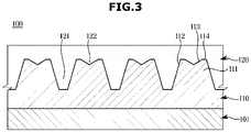
- FIG. 3 is a cross-sectional view schematically illustrating the optical film 100 shown in FIG. 2 .
- FIG. 4 is a graph illustrating the distribution of light emitted from a backlight unit shown in FIG. 2 .
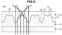
- FIG. 5 is a view schematically illustrating a state in which light, which is incident approximately perpendicular to the optical film shown in FIG. 3 , is refracted.
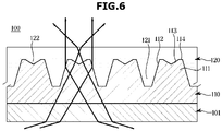
- FIG. 6 is a view schematically illustrating a state in which light, which is obliquely incident on the optical film shown in FIG. 3 , is refracted.
- the optical film 100 may include a base layer 101, a first refractive layer 110, and a second refractive layer 120.
- the base layer 101 may be positioned adjacent to the display panel 20.
- the base layer 101 may be positioned on one side closer to the display panel 20.
- the base layer 101 may be attached to the display panel 20.
- the base layer 101 may be positioned in front of the polarizing sheet 22 of the display panel 20.
- the base layer 101 may be positioned on the polarizing sheet 22.
- the base layer 101 may be attached to the polarizing sheet 22 of the display panel 20.
- the optical film 100 may be attached to the display panel 20 through an adhesive layer 91 (see FIG. 8 ).
- the optical film 100 may be attached to the polarizing sheet 22 through the adhesive layer 91.
- the base layer 101 may extend along a plane perpendicular to the front-rear direction. Light passing through the display panel 20 may pass through the base layer 101.
- the first refractive layer 110 may be positioned in front of the base layer 101.
- the first refractive layer 110 may extend along a plane perpendicular to the front-rear direction.
- a pattern 111 may be formed on the base layer 110.
- a plurality of patterns 111 may be continuously formed in the first refractive layer 110.
- the pattern 111 of the first refractive layer 110 may be formed in an embossed pattern. In some embodiments, the pattern 111 is repeated at a fixed interval as shown in FIG. 3 .
- the pattern 111 of the first refractive layer 110 may include a first inclined portion 112.
- the first inclined portion 112 may be configured to totally reflect some of the light waves emitted from the backlight unit 60.
- the first inclined portion 112 may be configured to totally reflect some of light waves passing through the base layer 101.
- the first inclined portion 112 may be configured to totally reflect light waves incident in the front and rear direction among the light waves emitted from the backlight unit 60.
- the first inclined portion 112 may be provided in plural.
- the first inclined portion 112 is part of the pattern 111, the pattern 111 is repeated across the optical film which creates a repetition of the first inclined portion at fixed intervals as shown in FIG. 3 .
- the first inclined portion 112 may be formed to be inclined with respect to a direction in which the first refractive layer 110 extends.
- the first inclined portion 112 may be formed to totally reflect that light, which is incident on the first refractive layer 110 in the front-rear direction, which has an incident angle greater than a critical angle.
- the first inclined portion 112 may form both sides of the pattern 111 with respect to the front-rear direction.
- the pattern 111 of the first refractive layer 110 may include a second inclined portion 113.
- the second inclined portion 113 may be formed to be inclined with respect to a direction in which the first refractive layer 110 extends.
- the second inclined portion 113 may be formed such that an inclination angle with respect to the direction in which the first refractive layer 110 extends is smaller than an inclination angle of the first inclined portion 112.
- the second inclined portion 113 may be provided repeatedly as shown in FIG. 3 .
- the second inclined portion 113 may be configured to refract light incident in the front-rear direction.
- the second inclined portion 113 may be configured to refract light incident obliquely with respect to the front-rear direction. For example, light arriving through the base layer at an oblique angle as shown in FIG. 6 may not be reflected by the first inclined portion 112 but may be incident on the second inclined portion 113 and be refracted thereby. Also, the second inclined portion 113 may be configured to refract light totally reflected by the first inclined portion 112.
- the pattern 111 of the first refractive layer 110 may include a parallel portion 114 extending in the same direction as the direction in which the first refractive layer 110 extends.
- the parallel portion 114 may extend in a direction perpendicular to the front-rear direction.
- the parallel portion 114 may be provided between the first inclined portion 112 and the second inclined portion 113.
- the proportion of light emitted in the front-rear direction may be high and the light emitted from the backlight unit 60 may include components of light emitted in a diagonal, or oblique, direction with respect to the front-rear direction.
- the light emitted in the front-rear direction in the backlight unit 60 and the light emitted in the oblique direction with respect to the front-rear direction may be incident on the optical film 100 after passing through the display panel 20.
- some of the light waves incident on the first refractive layer 110 in the front-rear direction may be incident on the first inclined portion 112.
- the light waves incident on the first inclined portion 112 may be totally reflected by the first inclined portion 112.
- the light waves totally reflected by the first inclined portion 112 may be incident on the second inclined portion 113.
- the light waves incident on the second inclined portion 113 may be refracted by the second inclined portion 113.
- the light waves refracted by the second inclined portion 113 may be emitted to the outside through the second refractive layer 120. Because the outside is an air layer and has a lower refractive index than the second refractive layer 120, the light waves may be refracted upon being emitted to the outside from the second refractive layer 120.
- the light waves emitted to the outside after total reflection by the first inclined portion 112 may have a relatively large emission angle in the front-rear direction.
- Some other of the light waves incident on the first refractive layer 110 in the front- rear direction may be incident on the second inclined portion 113.
- the light waves incident on the second inclined portion 113 may be refracted by the second inclined portion 113.
- the light waves refracted by the second inclined portion 113 may be emitted to the outside through the second refractive layer 120. Because the outside is an air layer and has a lower refractive index than the second refractive layer 120, the light waves may be refracted upon being emitted to the outside from the second refractive layer 120.
- Light waves emitted only through the refraction process in the second inclined portion 112 may have a moderate or medium emission angle in the front-rear direction.
- the parallel portion 114 may be incident on the parallel portion 114.
- the light waves incident on the first refractive layer 110 light waves, which are incident on the parallel portion 114 without passing through the first inclined portion 112 and / or the second inclined portion 113, may be emitted in the front-rear direction without being refracted by the parallel portion 114.
- light waves which are incident on the parallel portion 114 in a direction perpendicular to the parallel portion 114 will not be refracted.
- the light waves incident on the first refractive layer 110 light waves, which are incident on the parallel portion 114 after passing through the first inclined portion 112 and / or the second inclined portion 113, may be refracted at the parallel portion 114.
- light waves incident on the first refractive layer 110 in the front-rear directions may be emitted in the front-rear direction without being refracted at the first refractive layer 110.
- some of light waves incident obliquely with respect to the front-rear direction may be incident on the first inclined portion 112.
- the light waves incident on the first inclined portion 112 may be refracted by the first inclined portion 112.
- the light waves refracted by the first inclined portion 112 may be emitted to the outside through the second refractive layer 120. Because the outside is an air layer and has a lower refractive index than the second refractive layer 120, the light waves may be refracted upon being emitted to the outside from the second refractive layer 120.
- the light waves emitted after being refracted by the first inclined portion 112 may have a relatively small emission angle in the front-rear direction.
- Some other of the light waves incident obliquely with respect to the front-rear direction may be incident on the second inclined portion 113.
- the light waves incident on the second inclined portion 113 may be refracted by the second inclined portion 113.
- the light waves refracted by the second inclined portion 113 may be emitted to the outside through the second refractive layer 120. Because the outside is an air layer and has a lower refractive index than the second refractive layer 120, the light waves may be refracted upon being emitted to the outside from the second refractive layer 120.
- the light waves emitted after being refracted by the second inclined portion 113 may have a relatively medium emission angle in the front-rear direction.
- the second refractive layer 120 may be positioned in front of the first refractive layer 110.
- the second refractive layer 120 may have a lower refractive index than the refractive index of the first refractive layer 110. Because the second refractive layer 120 has a refractive index different from that of the first refractive layer 110, light waves passing sequentially through the first refractive layer 110 and the second refractive layer 120 may be totally reflected or refracted.
- the second refractive layer 120 may have a higher refractive index than the outer air layer.
- the second refractive layer 120 may include a filling portion 121 filling among the plurality of patterns 111.
- the filling portion 121 may be positioned in a groove between the patterns 111.
- the filling portion 121 may be formed to correspond to the size and shape of the grooves between the patterns 111.
- the filling portion 121 may be in contact with the first inclined portion 112.
- the second refractive layer 120 may include a supplement portion 122 positioned between the second inclined portions 113.
- the supplement portion 122 may be provided to be in contact with the second inclined portion 113 formed between the parallel portions 114.
- the supplement portion 122 may be positioned in the groove between the second inclined portions 113.
- the supplement portion 122 may be formed to correspond to the size and shape of the grooves between the second inclined portions 113.
- the display apparatus 1 may mix light waves emitted from the backlight unit 60 at various angles and emit the mixed light waves and thus it is possible to improve the viewing angle. That is, among the light waves emitted from the backlight unit 60, some light waves are totally reflected by the first inclined portion 112, refracted and emitted through the second refractive layer 120, and some other light waves are reflected by the second inclined portion 113 and emitted through the second refractive layer 120, and still other light waves are emitted by passing through the parallel portion 114 or between the patterns 111 without being refracted or total reflection. Therefore, the display apparatus 1 may emit the light waves at various angles.
- FIG. 7 is a graph illustrating the distribution of light emitted from a backlight unit according to another embodiment of the invention.
- a ratio of light emitted in the front-rear direction may be very high.
- the backlight unit 60 may be configured to minimize an amount of light emitted in the oblique direction with respect to the front-back direction and to maximize an amount of light in the front-rear direction.
- the backlight unit 60 may include a condensing film (not shown) for facilitating condensation.
- the display apparatus 1 includes the condensed backlight unit 60, most of the light waves emitted from the backlight unit 60 is totally reflected and / or refracted and emitted to the outside, as illustrated in FIG. 5 .
- FIG. 8 is a cross-sectional view schematically illustrating an optical film according to a comparative example not being part of the present invention.
- an optical film 200 may include a base layer 101, a first refractive layer 210, and a second refractive layer 120.
- the base layer 101 and the second refractive layer 120 are the same as those described with reference to FIGS. 3 to 6 , and thus a detailed description thereof will be omitted.
- a parallel portion 114 may be omitted in the first refractive layer 210 illustrated in FIG. 8 unlike the first refractive layer 110 illustrated in FIG. 3 .
- the first refractive layer 210 may include a pattern 211 formed in an embossed pattern.
- the pattern 211 may include a first inclined portion 212 and a second inclined portion 213.
- the first inclined portion 212 may totally reflect some of the light waves incident on the first refractive layer 210 in the front-rear direction.
- the light waves totally reflected by the first inclined portion 212 may be refracted by the second inclined portion 213 and have a large emission angle with respect to the front-rear direction and then emitted to the outside.
- the second inclined portion 213 may refract some other of the light waves incident on the first refractive layer 210 in the front-rear direction.
- the light waves refracted by the second inclined portion 213 have a medium emission angle with respect to the front-rear direction and then emitted to the outside.
- some light waves incident on the first inclined portion 212 may be refracted by the first inclined portion 212.
- the light waves refracted by the first inclined portion 212 have a small emission angle with respect to the front-rear direction and then emitted to the outside.
- some other light waves incident on the second inclined portion 213 may be refracted by the second inclined portion 213.
- the light waves refracted by the second inclined portion 213 have a medium emission angle with respect to the front-rear direction and then emitted to the outside.
- FIG. 9 is a cross-sectional view schematically illustrating an optical film according to yet another embodiment of the invention.
- an optical film 300 may include a base layer 101, a first refractive layer 310, and a second refractive layer 120.
- the base layer 101 and the second refractive layer 120 are the same as those described with reference to FIGS. 3 to 6 , and thus a detailed description thereof will be omitted.
- the first refractive layer 310 illustrated in FIG. 9 may further include a third inclined portion 315 and a fourth inclined portion 316, unlike the first refractive layer 110 illustrated in FIG. 3 .
- the first refractive layer 310 may include a pattern 311 formed in an embossed pattern.
- the pattern 311 may include a first inclined portion 312 and a second inclined portion 313, and a third inclined portion 315 and a fourth inclined portion 316.
- the first inclined portion 312 and the fourth inclined portion 316 may be inclined to have a large angle in a direction, in which the first refractive layer 310 extends, so as to totally reflect some of light waves incident in the front-rear direction.
- the second inclined portion 313 and the third inclined portion 315 may be inclined to have a smaller angle than the first inclined portion 312 and the fourth inclined portion 316, so as to refract light incident in the front-rear direction.
- the first inclined portion 312 and the fourth inclined portion 316 may totally reflect some of light waves incident on the first refractive layer 310 in the front-rear direction.
- the light waves totally reflected by the first inclined portion 312 may be refracted by the second inclined portion 313 and / or the fourth inclined portion 316, and have a large emission angle with respect to the front-rear direction and emitted to the outside.
- the light waves totally reflected by the first inclined portion 312 may be totally reflected again by the fourth inclined portion 316 and then refracted at the parallel portion 314 and / or the second refractive layer, and emitted at a large angle.
- the second inclined portion 313 and the third inclined portion 315 may refract some other of the light waves incident on the first refractive layer 310 in the front-rear direction.
- the light waves refracted by the second inclined portion 313 or the third inclined portion 315 may have a medium emission angle with respect to the front-rear direction and emitted to the outside.
- some light waves which are incident on the first inclined portion 312 or the fourth inclined portion 316, may be refracted by the first inclined portion 312 or the fourth inclined portion 316.
- the light waves refracted by the first inclined portion 312 or the fourth inclined portion 316 may have a small emission angle with respect to the front-rear directions and emitted to the outside.
- some other light waves, which are incident on the second inclined portion 313 or the third inclined portion 315 may be refracted by the second inclined portion 313 or the third inclined portion 315.
- the light waves refracted by the second inclined portion 313 or the third inclined portion 315 have a medium emission angle with respect to the front-rear direction and emitted to the outside.
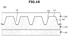
- FIG. 10 is a cross-sectional view schematically illustrating an optical film according to a comparative example not being part of the present invention.
- an optical film 400 may include a base layer 101, a first refractive layer 410, and a second refractive layer 120.
- the base layer 101 and the second refractive layer 120 are the same as those described with reference to FIGS. 3 to 6 , and thus a detailed description thereof will be omitted.
- the second inclined portion 113 may be omitted in the first refractive layer 410 illustrated in FIG. 10 , unlike the first refractive layer 110 illustrated in FIG. 3 .
- the first refractive layer 410 may include a pattern 411 formed in an embossed pattern.
- the pattern 411 may include a first inclined portion 412 and a parallel portion 414.
- a backlight unit 60 may use the backlight unit 60 having the emission distribution illustrated in FIG. 4 .
- the first inclined portion 412 may totally reflect some of light waves incident on the first refractive layer 410 in the front-rear direction.
- the light waves totally reflected by the first inclined portion 412 may be refracted by the parallel portion 414 and have a large emission angle with respect to the front-rear directions, and emitted to the outside.
- Some other of the light waves incident on the first refractive layer 410 in the front-rear directions may be incident on the parallel portion 414 or between the patterns 411, and pass through the parallel portion 414 or between the patterns 411, without the refraction.
- some light waves incident on the first inclined portion 412 may be refracted by the first inclined portion 412.
- the light waves refracted by the first inclined portion 412 may have a small emission angle with respect to the front-rear direction and emitted to the outside.
- the parallel portion 414 may be refracted at the parallel portion 414.
- the light waves refracted by the parallel portion 414 may have a medium emission angle with respect to the front-rear direction and emitted to the outside.
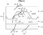
- FIG. 11 provides additional illustration of light waves passing through an optical film in accordance with embodiments of this invention.
- FIG. 11 illustrates the optical film of FIGS. 3 , 5 , 6 and 8-10 with additional labelling of angles.
- FIG. 11 illustrates the base layer 101, the first refractive layer 110 (with refractive index n 1 indicated by reference numeral 1113) the second refractive layer 120 (with refractive index n 2 indicated by reference numeral 1123) and the outside. In some embodiments, n 2 ⁇ n 1 .
- the direction in which the first refractive layer 110 extends is indicated with an arrow labelled 1131.
- a front-rear direction is indicated with an arrow labelled 1132.
- a normal direction to the first inclined portion 112 is indicated with a normal arrow labelled 1121.
- a normal direction to the second inclined portion 113 is indicated with a normal arrow labelled 1122 on first refractive layer 110 side and with a normal arrow labelled 1123 on the second refractive layer 120 side.
- Light waves 1195, 1190, 1100 and 1196 are illustrated in FIG. 11 .
- Light waves 1195 and 1190 impinge on the base layer 101.
- Light wave 1100 is first reflected and then refracted by the first refractive layer 110.
- Light wave 1196 is emitted to the outside.
- the light waves in some embodiments originate at the backlight 60 illustrated in FIG. 2 .
- the light wave 1100 is incident on the first inclined portion 112 at an angle ⁇ 1 with respect to the normal 1121.
- the light wave 1100 is totally reflected and then is incident at an angle ⁇ 2 with respect to the normal 1132 on the second inclined portion 113.
- the light wave 1100 passes through to the second refractive layer 120 at an angle ⁇ 3 with respect to the normal 1123.
- the front-rear direction is identified with the reference numeral 1132 and the direction in which the first refractive layer extends is identified with the reference numeral 1131.
- the incident light wave 1100 is incident in the direction 1132.
- light waves 1100 which are totally reflected by the first inclined portioned 112 are refracted by the second inclined portion 113.
- the incident light wave 1195 is incident at the rear surface of the base layer 101 at an angle ⁇ 7 with respect to the normal 1127 at the rear surface of the base layer 101.
- second light waves such as light wave 1190 may not be incident on the first inclined portion 112 (also see FIG. 6 showing light waves not incident on the first inclined portion 112).
- These second light waves enter the second refractive layer 120, after refraction, at a small angle with respect to the direction 1131.
- the second light waves In terms of the front-rear direction 1132 and passage of light through the second refractive layer 120, the second light waves have a larger angle than the light waves 1100 through the second refractive layer 120.
- the first refractive layer 110 is positioned in front of the base layer 101.
- the first refractive layer 110 includes a pattern and the pattern includes the first inclined portion 112, the parallel portion 114 and the second inclined portion 113. These portions each repeat in the pattern of the exemplary optical film 100 of FIG. 11 ; the pattern itself repeats in the direction 1131 (see, for example, FIG. 5 ).
- the first inclined portion is oriented with an angle ⁇ 4 1141 with respect to the direction 1131 (neglecting the +/- sense of direction 1131).
- the second inclined portion is oriented with an angle ⁇ 5 with respect to the direction 1131 (again neglecting the +/- sense of direction 1131). In some embodiments, ⁇ 5 ⁇ ⁇ 4 .
- a front surface of the second refractive layer 120 extends in the direction 1131 and thus has a normal vector 1126 which is parallel to the direction 1132.
- a large emission angle ⁇ 6 indicates that the light passing to the outside has a large angle with respect to the direction 1132 and thus with respect to normal 1126.
- the display apparatus may improve a viewing angle because the display apparatus includes an optical film having a refractive layer, in which an inclined portion configured to totally reflect some of incident light waves is formed.
- the display apparatus may be configured to allow external light to be incident on a refractive layer having a relatively low refractive index and then to be moved to a refractive layer having a relatively high refractive index, and thus the display apparatus may prevent retro-reflection caused by total reflection and improve the contrast ratio.
Landscapes
- Physics & Mathematics (AREA)
- Nonlinear Science (AREA)
- General Physics & Mathematics (AREA)
- Optics & Photonics (AREA)
- Mathematical Physics (AREA)
- Chemical & Material Sciences (AREA)
- Crystallography & Structural Chemistry (AREA)
- Planar Illumination Modules (AREA)
- Liquid Crystal (AREA)
- Devices For Indicating Variable Information By Combining Individual Elements (AREA)
Description
- The disclosure relates to a display apparatus, and more particularly to a display apparatus including an optical film.
- A display apparatus is a type of output device that visually displays data information such as characters, graphics, and images.
- The display apparatus may include an emissive type display panel such as an organic light emitting diode (OLED) panel, or a non-emissive type display panel such as a liquid crystal display (LCD) panel.
- A display apparatus having a liquid crystal display may include an optical film to improve a viewing angle. The optical film may include a plurality of refractive layers having different refractive indices. The optical film may improve the viewing angle of the display apparatus by utilizing the refraction phenomenon of light based on the refractive index difference among the plurality of refractive layers.
- However, there is a limit in improving the viewing angle of a display apparatus using only an optical film that utilizes a refraction phenomenon of light caused by a refractive index difference among the plurality of refractive layers. When a material capable of maximizing the refractive index is used, the manufacturing cost of the optical film is increased.
US2009/0256997 ,US2016/02526655 WO2012/005135 describe examples of the related art. - Therefore, as recited in the appended claims, the present invention provides a display apparatus having an improved viewing angle, being capable of reducing reflection of external light, and having an improved contrast ratio.
- Additional aspects of the present disclosure will be set forth in part in the description which follows and, in part, will be obvious from the description, or may be learned by practice of the present disclosure.
- These and/or other aspects of the invention will become apparent and more readily appreciated from the following description of embodiments, taken in conjunction with the accompanying drawings of which:
-
FIG. 1 is a view of a display apparatus according to an embodiment of the invention; -
FIG. 2 is an exploded view of the display apparatus shown inFIG. 1 ; -
FIG. 3 is a cross-sectional view schematically illustrating an optical film shown inFIG. 2 ; -
FIG. 4 is a graph illustrating the distribution of light emitted from a backlight unit shown inFIG. 2 ; -
FIG. 5 is a view schematically illustrating a state in which light, which is incident approximately perpendicular to the optical film shown inFIG. 3 , is refracted; -
FIG. 6 is a view schematically illustrating a state in which light, which is obliquely incident on the optical film shown inFIG. 3 , is refracted; -
FIG. 7 is a graph illustrating the distribution of light emitted from a backlight unit according to another embodiment of the invention; -
FIG. 8 is a cross-sectional view schematically illustrating an optical film according to a comparative example not being part of the present invention; -
FIG. 9 is a cross-sectional view schematically illustrating an optical film according to yet another embodiment of the invention; and -
FIG. 10 is a cross-sectional view schematically illustrating an optical film according to a comparative example not being part of the present invention. -
FIG. 11 indicates directions and angles of light waves passing through an exemplary optical film. - In the following description, like reference numerals refer to like elements throughout the specification. Well-known functions or constructions are not described in detail since they would obscure the one or more exemplary embodiments with unnecessary detail.
- It will be understood that when an element is referred to as being "connected" another element, it can be directly or indirectly connected to the other element, wherein the indirect connection includes "connection via a wireless communication network".
- Also, when a part "includes" or "comprises" an element, unless there is a particular description contrary thereto, the part may further include other elements, not excluding the other elements.
- Throughout the description, when a member is "on" another member, this includes not only when the member is in contact with the other member, but also when there is another member between the two members.
- It will be understood that, although the terms first, second, third, etc., may be used herein to describe various elements, but the disclosure is not limited by these terms. These terms are only used to distinguish one element from another element.
- As used herein, the singular forms "a," "an" and "the" are intended to include the plural forms as well, unless the context clearly indicates otherwise.
- An identification code is used for the convenience of the description but is not intended to illustrate the order of each step. The each step may be implemented in the order different from the illustrated order unless the context clearly indicates otherwise.
- Reference will now be made in detail to embodiments of the present invention, examples of which are illustrated in the accompanying drawings.
-
FIG. 1 is a view of a display apparatus according to an embodiment of the invention.FIG. 2 is an exploded view of the display apparatus shown inFIG. 1 . - Referring to
FIGS. 1 and2 , according to an embodiment of the invention, a display apparatus 1 includes atop chassis 10, adisplay panel 20, abacklight unit 60, and abottom chassis 70. Thetop chassis 10 is positioned in front of thedisplay panel 20. Thedisplay panel 20 may be positioned in front of thebacklight unit 60. Thebacklight unit 60 is positioned behind thedisplay panel 20 to be apart from thedisplay panel 20. Thebottom chassis 70 may be positioned behind thedisplay panel 20 and thebacklight unit 60. - A middle mold 40 may be further provided between the
display panel 20 and thebacklight unit 60. The middle mold 40 may allow thedisplay panel 20 to be supported apart from thebacklight unit 60. A printedcircuit board 80 configured to control a drive of the display apparatus 1 may be positioned behind thebottom chassis 70. Arear cover 15 forming a rear outer appearance of the display apparatus 1 may be provided behind the printedcircuit board 80. - A plurality of
optical sheets 30 may be provided behind thedisplay panel 20. Alight guide plate 50 may be positioned behind the plurality ofoptical sheets 30. Areflective sheet 55 may be positioned behind thelight guide plate 50. - The plurality of
optical sheets 30 include aprotective film 31, aprism film 32, and adiffusion film 33. Theprotective film 31 is positioned in front of theprism film 32 to protect theprism film 32 sensitive to scratches such as dust. - A triangular prism may be positioned in front of the
prism film 32. Through theprism film 32, light diffused by thediffusion film 33 may be focused on a direction perpendicular to a rear surface of thedisplay panel 20. Twoprism films 32 may be used. The light passing through theprism film 32 may travel perpendicularly to thedisplay panel 20 so as to allow thedisplay panel 20 to have a uniform brightness. Light passing through thelight guide plate 50 may be diffused by thediffusion film 33 and supplied to thedisplay panel 20. - The
light guide plate 50 may be configured to allow light emitted from alight emitting diode 61 to be uniformly supplied to thediffusion film 33. Thelight guide plate 50 may include anexit surface 51 and anincident surface 52. Theexit surface 51 may be located behind thediffusion film 33 and face one surface of thediffusion film 33. Theincident surface 52 may be provided on the side surface and on which light emitted from thelight emitting diode 61 is incident. - The
reflective sheet 55 may be positioned behind thelight guide plate 50. Light emitted through a lower surface of thelight guide plate 50 may be guided to thelight guide plate 50 again by thereflective sheet 55. - The
backlight unit 60 includes a plurality oflight emitting diodes 61 and a printedcircuit board 62. Thebacklight unit 60 may be configured to emit light. Thelight emitting diode 61 may supply light to thelight guide plate 50. The plurality oflight emitting diodes 61 may be mounted on the printedcircuit board 62. - The plurality of
light emitting diodes 61 may be mounted to protrude from one surface of the printedcircuit board 62. The plurality oflight emitting diodes 61 may be arranged on a surface of the printedcircuit board 62 at a predetermined distance. - The printed
circuit board 62 may be positioned behind thereflective sheet 55. The printedcircuit board 62 may be fixed to thebottom chassis 70 via a fastening member such as a screw or an attachment means such as a double-sided tape. As for the printedcircuit board 62, a back surface of a surface on which the plurality oflight emitting diodes 61 are mounted, may be fixed to abottom surface 72 of thebottom chassis 70. - The
display panel 20 may include afirst substrate 211 having a thin film transistor (TFT) and a pixel electrode, and asecond substrate 210 positioned on one side of thefirst substrate 211 and provided with a color filter and a driving source. Aliquid crystal layer 212 may be provided between thefirst substrate 211 and thesecond substrate 210. Polarizingsheets first substrate 211 and / or the front of thesecond substrate 210. A module in which thefirst substrate 211, thesecond substrate 210, and theliquid crystal layer 212 are combined may be referred to as a liquidcrystal display module 21. - A
driver 25 applying a driving signal may be provided on one side of thefirst substrate 211. Thedriver 25 may include a flexible printedcircuit board 26, adriving chip 27, and acircuit board 28. Thedriving chip 27 may be mounted on one side of the flexible printedcircuit board 26. Thecircuit board 28 may be connected to the other side of the flexible printedcircuit board 26. - A black matrix (not shown) may be formed on the
second substrate 210. A cable to which thedriver 25 and the printedcircuit board 80 are connected may pass through the rear space of the black matrix. - The
display panel 20 may form a screen by adjusting the arrangement of theliquid crystal layer 212. As a non-light emitting element, thedisplay panel 20 may receive light from thebacklight unit 60 and display an image. - An
optical film 100 improving a viewing angle and / or a contrast ratio may be positioned in front of thedisplay panel 20. Details of theoptical film 100 will be described later. - The
top chassis 10 may include abezel 11 and a toplateral side 12. Thebezel 11 may cover the front edge of thedisplay panel 20. The toplateral side 12 may be bent downward from an end portion of thebezel 11. At least a part of the toplateral side 12 may be in contact with thebottom chassis 70. For example, at least one part of the toplateral side 12 may cover the outer side of a bottomlateral side 71. - The
top chassis 10 may be provided with anopening 13 through which thedisplay panel 20 is exposed. An effective display area, in which a screen is actually displayed on thedisplay panel 20, may be exposed to the front side through theopening 13. - The
bottom chassis 70 may include the bottomlateral side 71 and thebottom surface 72. The bottomlateral side 71 may extend upwardly along the circumference of thebottom surface 72. Thebacklight unit 60 may be seated on thebottom surface 72. A heat radiation sheet (not shown) may be positioned behind thebottom surface 72 of thebottom chassis 70. - The middle mold 40 may include a
first support portion 40a, asecond support portion 40b, and an extension portion 40c. Thefirst support portion 40a and thesecond support portion 40b may extend to the inside of the middle mold 40. Thesecond support portion 40b may extend inward from thefirst support portion 40a and extend downward from thefirst support portion 40a to be stepped. The extension portion 40c extends to the lower side of the middle mold 40. A part of thedisplay panel 20 may be supported by thefirst support portion 40a. A part of theoptical sheet 30 may be supported by thesecond support portion 40b. An outer surface of the extension portion 40c may be in contact with the inner surface of thebottom chassis 70. - The
light emitting diode 61 may simultaneously emit light and heat. The printedcircuit board 62 may serve not only to supply a driving signal to thelight emitting diode 61 but also to transmit the heat generated by thelight emitting diode 61 to the outside. That is, the heat generated in thelight emitting diode 61 may be transmitted to thebottom chassis 70 through the printedcircuit board 62. The printedcircuit board 62 may be formed of a metal having a high thermal conductivity to increase heat transfer efficiency. For example, the printedcircuit board 62 may be formed of a metal material including aluminum or copper. - A printed
circuit board 80 may be mounted on the rear side of thebottom chassis 70. Therear cover 15 may be located behind the printedcircuit board 80. The printedcircuit board 80 may include a printed circuit board 81 and a plurality of electronic components mounted on the printed circuit board 81. The electronic components may be mounted on the upper surface and / or the lower surface of the printed circuit board 81. The plurality of electronic components may be mounted on or fixed to the printed circuit board 82 by a clamp. -
FIG. 3 is a cross-sectional view schematically illustrating theoptical film 100 shown inFIG. 2 .FIG. 4 is a graph illustrating the distribution of light emitted from a backlight unit shown inFIG. 2 .FIG. 5 is a view schematically illustrating a state in which light, which is incident approximately perpendicular to the optical film shown inFIG. 3 , is refracted.FIG. 6 is a view schematically illustrating a state in which light, which is obliquely incident on the optical film shown inFIG. 3 , is refracted. - Referring to
FIG. 3 , theoptical film 100 may include abase layer 101, a firstrefractive layer 110, and a secondrefractive layer 120. - The
base layer 101 may be positioned adjacent to thedisplay panel 20. Thebase layer 101 may be positioned on one side closer to thedisplay panel 20. Thebase layer 101 may be attached to thedisplay panel 20. Thebase layer 101 may be positioned in front of thepolarizing sheet 22 of thedisplay panel 20. Thebase layer 101 may be positioned on thepolarizing sheet 22. Thebase layer 101 may be attached to thepolarizing sheet 22 of thedisplay panel 20. Theoptical film 100 may be attached to thedisplay panel 20 through an adhesive layer 91 (seeFIG. 8 ). Theoptical film 100 may be attached to thepolarizing sheet 22 through theadhesive layer 91. - The
base layer 101 may extend along a plane perpendicular to the front-rear direction. Light passing through thedisplay panel 20 may pass through thebase layer 101. - The first
refractive layer 110 may be positioned in front of thebase layer 101. The firstrefractive layer 110 may extend along a plane perpendicular to the front-rear direction. Apattern 111 may be formed on thebase layer 110. A plurality ofpatterns 111 may be continuously formed in the firstrefractive layer 110. Thepattern 111 of the firstrefractive layer 110 may be formed in an embossed pattern. In some embodiments, thepattern 111 is repeated at a fixed interval as shown inFIG. 3 . - The
pattern 111 of the firstrefractive layer 110 may include a firstinclined portion 112. The firstinclined portion 112 may be configured to totally reflect some of the light waves emitted from thebacklight unit 60. The firstinclined portion 112 may be configured to totally reflect some of light waves passing through thebase layer 101. The firstinclined portion 112 may be configured to totally reflect light waves incident in the front and rear direction among the light waves emitted from thebacklight unit 60. The firstinclined portion 112 may be provided in plural. In some embodiments, the firstinclined portion 112 is part of thepattern 111, thepattern 111 is repeated across the optical film which creates a repetition of the first inclined portion at fixed intervals as shown inFIG. 3 . - The first
inclined portion 112 may be formed to be inclined with respect to a direction in which the firstrefractive layer 110 extends. The firstinclined portion 112 may be formed to totally reflect that light, which is incident on the firstrefractive layer 110 in the front-rear direction, which has an incident angle greater than a critical angle. The firstinclined portion 112 may form both sides of thepattern 111 with respect to the front-rear direction. - The
pattern 111 of the firstrefractive layer 110 may include a secondinclined portion 113. The secondinclined portion 113 may be formed to be inclined with respect to a direction in which the firstrefractive layer 110 extends. The secondinclined portion 113 may be formed such that an inclination angle with respect to the direction in which the firstrefractive layer 110 extends is smaller than an inclination angle of the firstinclined portion 112. The secondinclined portion 113 may be provided repeatedly as shown inFIG. 3 . - The second
inclined portion 113 may be configured to refract light incident in the front-rear direction. The secondinclined portion 113 may be configured to refract light incident obliquely with respect to the front-rear direction. For example, light arriving through the base layer at an oblique angle as shown inFIG. 6 may not be reflected by the firstinclined portion 112 but may be incident on the secondinclined portion 113 and be refracted thereby. Also, the secondinclined portion 113 may be configured to refract light totally reflected by the firstinclined portion 112. - The
pattern 111 of the firstrefractive layer 110 may include aparallel portion 114 extending in the same direction as the direction in which the firstrefractive layer 110 extends. Theparallel portion 114 may extend in a direction perpendicular to the front-rear direction. Theparallel portion 114 may be provided between the firstinclined portion 112 and the secondinclined portion 113. - Particularly, referring to
FIG. 4 , as for the light emitted from thebacklight unit 60, the proportion of light emitted in the front-rear direction may be high and the light emitted from thebacklight unit 60 may include components of light emitted in a diagonal, or oblique, direction with respect to the front-rear direction. The light emitted in the front-rear direction in thebacklight unit 60 and the light emitted in the oblique direction with respect to the front-rear direction may be incident on theoptical film 100 after passing through thedisplay panel 20. - Referring to
FIG. 5 , some of the light waves incident on the firstrefractive layer 110 in the front-rear direction may be incident on the firstinclined portion 112. The light waves incident on the firstinclined portion 112 may be totally reflected by the firstinclined portion 112. The light waves totally reflected by the firstinclined portion 112 may be incident on the secondinclined portion 113. The light waves incident on the secondinclined portion 113 may be refracted by the secondinclined portion 113. The light waves refracted by the secondinclined portion 113 may be emitted to the outside through the secondrefractive layer 120. Because the outside is an air layer and has a lower refractive index than the secondrefractive layer 120, the light waves may be refracted upon being emitted to the outside from the secondrefractive layer 120. The light waves emitted to the outside after total reflection by the firstinclined portion 112 may have a relatively large emission angle in the front-rear direction. - Some other of the light waves incident on the first
refractive layer 110 in the front- rear direction may be incident on the secondinclined portion 113. The light waves incident on the secondinclined portion 113 may be refracted by the secondinclined portion 113. The light waves refracted by the secondinclined portion 113 may be emitted to the outside through the secondrefractive layer 120. Because the outside is an air layer and has a lower refractive index than the secondrefractive layer 120, the light waves may be refracted upon being emitted to the outside from the secondrefractive layer 120. Light waves emitted only through the refraction process in the secondinclined portion 112 may have a moderate or medium emission angle in the front-rear direction. - Still some other of the light waves incident on the first
refractive layer 110 in the front-rear directions may be incident on theparallel portion 114. Among the light waves incident on the firstrefractive layer 110, light waves, which are incident on theparallel portion 114 without passing through the firstinclined portion 112 and / or the secondinclined portion 113, may be emitted in the front-rear direction without being refracted by theparallel portion 114. For example, light waves which are incident on theparallel portion 114 in a direction perpendicular to theparallel portion 114 will not be refracted. Among the light waves incident on the firstrefractive layer 110, light waves, which are incident on theparallel portion 114 after passing through the firstinclined portion 112 and / or the secondinclined portion 113, may be refracted at theparallel portion 114. - Among the light waves incident on the first
refractive layer 110 in the front-rear directions, light waves incident between thepatterns 111 may be emitted in the front-rear direction without being refracted at the firstrefractive layer 110. - Referring to
FIG. 6 , some of light waves incident obliquely with respect to the front-rear direction may be incident on the firstinclined portion 112. The light waves incident on the firstinclined portion 112 may be refracted by the firstinclined portion 112. The light waves refracted by the firstinclined portion 112 may be emitted to the outside through the secondrefractive layer 120. Because the outside is an air layer and has a lower refractive index than the secondrefractive layer 120, the light waves may be refracted upon being emitted to the outside from the secondrefractive layer 120. The light waves emitted after being refracted by the firstinclined portion 112 may have a relatively small emission angle in the front-rear direction. - Some other of the light waves incident obliquely with respect to the front-rear direction may be incident on the second
inclined portion 113. The light waves incident on the secondinclined portion 113 may be refracted by the secondinclined portion 113. The light waves refracted by the secondinclined portion 113 may be emitted to the outside through the secondrefractive layer 120. Because the outside is an air layer and has a lower refractive index than the secondrefractive layer 120, the light waves may be refracted upon being emitted to the outside from the secondrefractive layer 120. The light waves emitted after being refracted by the secondinclined portion 113 may have a relatively medium emission angle in the front-rear direction. - The second
refractive layer 120 may be positioned in front of the firstrefractive layer 110. The secondrefractive layer 120 may have a lower refractive index than the refractive index of the firstrefractive layer 110. Because the secondrefractive layer 120 has a refractive index different from that of the firstrefractive layer 110, light waves passing sequentially through the firstrefractive layer 110 and the secondrefractive layer 120 may be totally reflected or refracted. The secondrefractive layer 120 may have a higher refractive index than the outer air layer. - The second
refractive layer 120 may include a fillingportion 121 filling among the plurality ofpatterns 111. The fillingportion 121 may be positioned in a groove between thepatterns 111. The fillingportion 121 may be formed to correspond to the size and shape of the grooves between thepatterns 111. The fillingportion 121 may be in contact with the firstinclined portion 112. - The second
refractive layer 120 may include asupplement portion 122 positioned between the secondinclined portions 113. Thesupplement portion 122 may be provided to be in contact with the secondinclined portion 113 formed between theparallel portions 114. Thesupplement portion 122 may be positioned in the groove between the secondinclined portions 113. Thesupplement portion 122 may be formed to correspond to the size and shape of the grooves between the secondinclined portions 113. - Because the display apparatus 1 according to an embodiment of the invention includes the
optical film 100 having the above-described configuration, the display apparatus 1 may mix light waves emitted from thebacklight unit 60 at various angles and emit the mixed light waves and thus it is possible to improve the viewing angle. That is, among the light waves emitted from thebacklight unit 60, some light waves are totally reflected by the firstinclined portion 112, refracted and emitted through the secondrefractive layer 120, and some other light waves are reflected by the secondinclined portion 113 and emitted through the secondrefractive layer 120, and still other light waves are emitted by passing through theparallel portion 114 or between thepatterns 111 without being refracted or total reflection. Therefore, the display apparatus 1 may emit the light waves at various angles. - In addition, because external light is incident on the first
refractive layer 110 after passing through the secondrefractive layer 120 having a relatively low refractive index, it is possible to prevent retro reflection caused by the total reflection, and thus it is possible to reduce the glare caused by the external light. -
FIG. 7 is a graph illustrating the distribution of light emitted from a backlight unit according to another embodiment of the invention. - Hereinafter a description the same as those described in
FIGS. 3 to 6 will be omitted. - Referring to
FIG. 7 , as for light emitted from abacklight unit 60, a ratio of light emitted in the front-rear direction may be very high. Thebacklight unit 60 may be configured to minimize an amount of light emitted in the oblique direction with respect to the front-back direction and to maximize an amount of light in the front-rear direction. Thebacklight unit 60 may include a condensing film (not shown) for facilitating condensation. - When the display apparatus 1 includes the condensed
backlight unit 60, most of the light waves emitted from thebacklight unit 60 is totally reflected and / or refracted and emitted to the outside, as illustrated inFIG. 5 . -
FIG. 8 is a cross-sectional view schematically illustrating an optical film according to a comparative example not being part of the present invention. - Hereinafter a description the same as those described in
FIGS. 3 to 6 will be omitted. - Referring to
FIG. 8 , anoptical film 200 may include abase layer 101, a firstrefractive layer 210, and a secondrefractive layer 120. Thebase layer 101 and the secondrefractive layer 120 are the same as those described with reference toFIGS. 3 to 6 , and thus a detailed description thereof will be omitted. - A
parallel portion 114 may be omitted in the firstrefractive layer 210 illustrated inFIG. 8 unlike the firstrefractive layer 110 illustrated inFIG. 3 . The firstrefractive layer 210 may include apattern 211 formed in an embossed pattern. Thepattern 211 may include a firstinclined portion 212 and a secondinclined portion 213. - The first
inclined portion 212 may totally reflect some of the light waves incident on the firstrefractive layer 210 in the front-rear direction. The light waves totally reflected by the firstinclined portion 212 may be refracted by the secondinclined portion 213 and have a large emission angle with respect to the front-rear direction and then emitted to the outside. - The second
inclined portion 213 may refract some other of the light waves incident on the firstrefractive layer 210 in the front-rear direction. The light waves refracted by the secondinclined portion 213 have a medium emission angle with respect to the front-rear direction and then emitted to the outside. - Among light waves incident obliquely with respect to the front-rear direction, some light waves incident on the first
inclined portion 212 may be refracted by the firstinclined portion 212. The light waves refracted by the firstinclined portion 212 have a small emission angle with respect to the front-rear direction and then emitted to the outside. - Among the light waves incident obliquely with respect to the front-rear direction, some other light waves incident on the second
inclined portion 213 may be refracted by the secondinclined portion 213. The light waves refracted by the secondinclined portion 213 have a medium emission angle with respect to the front-rear direction and then emitted to the outside. -
FIG. 9 is a cross-sectional view schematically illustrating an optical film according to yet another embodiment of the invention. - Hereinafter a description the same as those described in
FIGS. 3 to 6 will be omitted. - Referring to
FIG. 9 , anoptical film 300 may include abase layer 101, a firstrefractive layer 310, and a secondrefractive layer 120. Thebase layer 101 and the secondrefractive layer 120 are the same as those described with reference toFIGS. 3 to 6 , and thus a detailed description thereof will be omitted. - The first
refractive layer 310 illustrated inFIG. 9 may further include a thirdinclined portion 315 and a fourthinclined portion 316, unlike the firstrefractive layer 110 illustrated inFIG. 3 . The firstrefractive layer 310 may include apattern 311 formed in an embossed pattern. Thepattern 311 may include a firstinclined portion 312 and a secondinclined portion 313, and a thirdinclined portion 315 and a fourthinclined portion 316. - The first
inclined portion 312 and the fourthinclined portion 316 may be inclined to have a large angle in a direction, in which the firstrefractive layer 310 extends, so as to totally reflect some of light waves incident in the front-rear direction. The secondinclined portion 313 and the thirdinclined portion 315 may be inclined to have a smaller angle than the firstinclined portion 312 and the fourthinclined portion 316, so as to refract light incident in the front-rear direction. - The first
inclined portion 312 and the fourthinclined portion 316 may totally reflect some of light waves incident on the firstrefractive layer 310 in the front-rear direction. The light waves totally reflected by the firstinclined portion 312 may be refracted by the secondinclined portion 313 and / or the fourthinclined portion 316, and have a large emission angle with respect to the front-rear direction and emitted to the outside. Alternatively, the light waves totally reflected by the firstinclined portion 312 may be totally reflected again by the fourthinclined portion 316 and then refracted at theparallel portion 314 and / or the second refractive layer, and emitted at a large angle. - The second
inclined portion 313 and the thirdinclined portion 315 may refract some other of the light waves incident on the firstrefractive layer 310 in the front-rear direction. The light waves refracted by the secondinclined portion 313 or the thirdinclined portion 315 may have a medium emission angle with respect to the front-rear direction and emitted to the outside. - Among the light waves incident obliquely with respect to the front-rear direction, some light waves, which are incident on the first
inclined portion 312 or the fourthinclined portion 316, may be refracted by the firstinclined portion 312 or the fourthinclined portion 316. The light waves refracted by the firstinclined portion 312 or the fourthinclined portion 316 may have a small emission angle with respect to the front-rear directions and emitted to the outside. - Among the light waves incident obliquely with respect to the front-rear direction, some other light waves, which are incident on the second
inclined portion 313 or the thirdinclined portion 315 may be refracted by the secondinclined portion 313 or the thirdinclined portion 315. The light waves refracted by the secondinclined portion 313 or the thirdinclined portion 315 have a medium emission angle with respect to the front-rear direction and emitted to the outside. -
FIG. 10 is a cross-sectional view schematically illustrating an optical film according to a comparative example not being part of the present invention. - Hereinafter a description the same as those described in
FIGS. 3 to 6 will be omitted. - Referring to
FIG. 10 , anoptical film 400 may include abase layer 101, a firstrefractive layer 410, and a secondrefractive layer 120. Thebase layer 101 and the secondrefractive layer 120 are the same as those described with reference toFIGS. 3 to 6 , and thus a detailed description thereof will be omitted. - The second
inclined portion 113 may be omitted in the firstrefractive layer 410 illustrated inFIG. 10 , unlike the firstrefractive layer 110 illustrated inFIG. 3 . The firstrefractive layer 410 may include apattern 411 formed in an embossed pattern. Thepattern 411 may include a first inclined portion 412 and aparallel portion 414. Abacklight unit 60 may use thebacklight unit 60 having the emission distribution illustrated inFIG. 4 . - The first inclined portion 412 may totally reflect some of light waves incident on the first
refractive layer 410 in the front-rear direction. The light waves totally reflected by the first inclined portion 412 may be refracted by theparallel portion 414 and have a large emission angle with respect to the front-rear directions, and emitted to the outside. - Some other of the light waves incident on the first
refractive layer 410 in the front-rear directions may be incident on theparallel portion 414 or between thepatterns 411, and pass through theparallel portion 414 or between thepatterns 411, without the refraction. - Among the light waves incident obliquely with respect to the front-rear direction, some light waves incident on the first inclined portion 412 may be refracted by the first inclined portion 412. The light waves refracted by the first inclined portion 412 may have a small emission angle with respect to the front-rear direction and emitted to the outside.
- Among the light waves incident obliquely with respect to the front-rear direction, still some other light waves, which are incident on the
parallel portion 414, may be refracted at theparallel portion 414. The light waves refracted by theparallel portion 414 may have a medium emission angle with respect to the front-rear direction and emitted to the outside. -
FIG. 11 provides additional illustration of light waves passing through an optical film in accordance with embodiments of this invention.FIG. 11 illustrates the optical film ofFIGS. 3 ,5 ,6 and8-10 with additional labelling of angles.FIG. 11 illustrates thebase layer 101, the first refractive layer 110 (with refractive index n1 indicated by reference numeral 1113) the second refractive layer 120 (with refractive index n2 indicated by reference numeral 1123) and the outside. In some embodiments, n2 < n1. The direction in which the firstrefractive layer 110 extends is indicated with an arrow labelled 1131. A front-rear direction is indicated with an arrow labelled 1132. A normal direction to the firstinclined portion 112 is indicated with a normal arrow labelled 1121. A normal direction to the secondinclined portion 113 is indicated with a normal arrow labelled 1122 on firstrefractive layer 110 side and with a normal arrow labelled 1123 on the secondrefractive layer 120 side. -
Light waves FIG. 11 .Light waves base layer 101.Light wave 1100 is first reflected and then refracted by the firstrefractive layer 110.Light wave 1196 is emitted to the outside. The light waves, in some embodiments originate at thebacklight 60 illustrated inFIG. 2 . InFIG. 11 , thelight wave 1100 is incident on the firstinclined portion 112 at an angle θ1 with respect to the normal 1121. In the example ofFIG. 11 , thelight wave 1100 is totally reflected and then is incident at an angle θ2 with respect to the normal 1132 on the secondinclined portion 113. Thelight wave 1100 passes through to the secondrefractive layer 120 at an angle θ3 with respect to the normal 1123. - In
FIG. 11 , the front-rear direction is identified with thereference numeral 1132 and the direction in which the first refractive layer extends is identified with thereference numeral 1131. In some embodiments, theincident light wave 1100 is incident in thedirection 1132. - Thus, in some embodiments,
light waves 1100 which are totally reflected by the first inclined portioned 112 are refracted by the secondinclined portion 113. - In comparison, the
incident light wave 1195 is incident at the rear surface of thebase layer 101 at an angle θ7 with respect to the normal 1127 at the rear surface of thebase layer 101. Depending on geometry, second light waves such aslight wave 1190 may not be incident on the first inclined portion 112 (also seeFIG. 6 showing light waves not incident on the first inclined portion 112). These second light waves, in some embodiments, enter the secondrefractive layer 120, after refraction, at a small angle with respect to thedirection 1131. In terms of the front-rear direction 1132 and passage of light through the secondrefractive layer 120, the second light waves have a larger angle than thelight waves 1100 through the secondrefractive layer 120. - In the example of
FIG. 11 , the firstrefractive layer 110 is positioned in front of thebase layer 101. The firstrefractive layer 110 includes a pattern and the pattern includes the firstinclined portion 112, theparallel portion 114 and the secondinclined portion 113. These portions each repeat in the pattern of the exemplaryoptical film 100 ofFIG. 11 ; the pattern itself repeats in the direction 1131 (see, for example,FIG. 5 ). - The first inclined portion is oriented with an angle θ4 1141 with respect to the direction 1131 (neglecting the +/- sense of direction 1131). The second inclined portion is oriented with an angle θ5 with respect to the direction 1131 (again neglecting the +/- sense of direction 1131). In some embodiments, θ5 < θ4.
- After passage through the second
refractive layer 120, light waves pass to the outside (inFIG. 11 seelight wave 1196 at emission angle θ6, also, see, for example,FIGS. 5-6 ). In some embodiments, a front surface of the secondrefractive layer 120 extends in thedirection 1131 and thus has anormal vector 1126 which is parallel to thedirection 1132. A large emission angle θ6, in some embodiments, indicates that the light passing to the outside has a large angle with respect to thedirection 1132 and thus with respect to normal 1126. For example, the emission angle may be an angle of θ6 = 60 degrees up to θ6 = 90 degrees. An emission angle of θ6 = 90 degrees indicates a light wave parallel to thedirection 1131. A small emission angle θ6, in some embodiments, indicates that the light passing to the outside has a small angle with respect to thedirection 1132, for example, an angle of θ6 = 0 degrees up to θ6 = 30 degrees. θ6 = 0 degrees corresponds to a light wave parallel to thedirection 1132 and thus parallel to the normal 1126 at the front surface of the secondrefractive layer 120. Between these large and small angles, a medium emission angle θ6, in some embodiments, has values between θ6 = 30 degrees to θ6 = 60 degrees with respect to thedirection 1132 and similarly with normal 1126. - As is apparent from the above description, the display apparatus may improve a viewing angle because the display apparatus includes an optical film having a refractive layer, in which an inclined portion configured to totally reflect some of incident light waves is formed.
- The display apparatus may be configured to allow external light to be incident on a refractive layer having a relatively low refractive index and then to be moved to a refractive layer having a relatively high refractive index, and thus the display apparatus may prevent retro-reflection caused by total reflection and improve the contrast ratio.
- Although a few embodiments of the present invention have been shown and described, it would be appreciated by those skilled in the art that changes may be made in these embodiments without departing from the scope of the claims.
Claims (9)
- A display apparatus (1) comprising:a backlight unit (60) configured to emit a plurality of light waves, wherein the plurality of light waves includes a first plurality of light waves;a display panel (20) positioned in front of the backlight unit (60); andan optical film (100) positioned in front of the display panel (20),wherein the optical film (100) comprises:a base layer (101) positioned adjacent to the display panel (20);a first refractive layer (110) positioned in front of the base layer (101) and associated with a first refractive index, wherein the first refractive layer (110) includes a pattern (111) and the pattern includes afirst inclined portion (112), whereby the first plurality of light waves comprises those light waves emitted after having undergone a total reflection by the first inclined portion (112); anda second refractive layer (120) positioned in front of the first refractive layer (110), wherein the second refractive layer (120) is associated with a second refractive index and the second refractive index is less than the first refractive index,characterized in that the pattern (111) further includes :a pair of second inclined portions (113) formed to define a groove; anda parallel portion (114) parallel to the direction in which the first refractive layer (110) extends, the parallel portion (114) being provided between the first inclined portion (112) and the pair of second inclined portion (113); and in thatthe second refractive layer (120) comprises a supplement portion (122) provided to be in contact with the pair of second inclined portions (113); andthe supplement portion (122) is configured to correspond to the size and shape of the groove formed by the pair of second inclined portions (113).
- The display apparatus of claim 1, wherein
the first inclined portion (112) is oriented at a first angle with respect to the direction in which the first refractive layer (110) extends, wherein each of the pair of second inclined portions (113) is inclined at a second angle with respect to the direction in which the first refractive layer (110) extends, and wherein the second angle is smaller than the first angle. - The display apparatus of claim 2, wherein each of the pair of second inclined portions (113) is configured to refract the first plurality of light waves.
- The display apparatus of claim 2, wherein
the plurality of light waves includes a second plurality of light waves emitted without having undergone a total reflection by the first inclined portion (112), and wherein the optical film (100) is configured such that those light waves among the first plurality of light waves which are incident on the optical film (100) in a front-rear direction (1132) are emitted at an angle with respect to a front-rear direction (1132) which is larger than the angle at which those light waves among the second plurality of light waves which are incident on the optical film (100) in a front-rear direction (1132) are emitted. - The display apparatus of claim 2, wherein
the plurality of light waves includes a third plurality of light waves which are obliquely incident on the optical film (100) with respect to a front-rear direction (1132) and wherein the optical film (100) is configured such that those light waves among the third plurality of light waves emitted after having been refracted by the first inclined portion (112) are emitted at a smaller angle with respect to the front-rear direction (1132) than those light waves among the third plurality of light waves emitted after having been refracted by the pair of second inclined portions (113). - The display apparatus of claim 1, wherein
the pattern (111) of the first refractive layer (110) is formed in an embossed pattern. - The display apparatus of claim 6, wherein
the second refractive layer (120) comprises a filling portion (121) filling between the patterns (111) of the first refractive layer (110). - The display apparatus of claim 1, further comprising:
an adhesive layer (91) positioned between the display panel (20) and the optical film (100). - The display apparatus of claim 1, whereinthe display panel (20) comprises a polarizing sheet (22), andwherein the base layer (101) is positioned in front of the polarizing sheet (22).
Applications Claiming Priority (1)
| Application Number | Priority Date | Filing Date | Title |
|---|---|---|---|
| KR1020180087822A KR102723985B1 (en) | 2018-07-27 | 2018-07-27 | Display apparatus |
Publications (2)
| Publication Number | Publication Date |
|---|---|
| EP3599505A1 EP3599505A1 (en) | 2020-01-29 |
| EP3599505B1 true EP3599505B1 (en) | 2021-09-08 |
Family
ID=67438959
Family Applications (1)
| Application Number | Title | Priority Date | Filing Date |
|---|---|---|---|
| EP19188471.7A Active EP3599505B1 (en) | 2018-07-27 | 2019-07-25 | Display apparatus |
Country Status (4)
| Country | Link |
|---|---|
| US (1) | US11333918B2 (en) |
| EP (1) | EP3599505B1 (en) |
| KR (1) | KR102723985B1 (en) |
| WO (1) | WO2020022630A1 (en) |
Families Citing this family (2)
| Publication number | Priority date | Publication date | Assignee | Title |
|---|---|---|---|---|
| CN114002879B (en) | 2021-11-01 | 2023-06-30 | 深圳市华星光电半导体显示技术有限公司 | Optical film and display device |
| CN116880104B (en) * | 2023-08-31 | 2023-12-05 | 北京小米移动软件有限公司 | Light guide components, display components and electronic equipment |
Family Cites Families (13)
| Publication number | Priority date | Publication date | Assignee | Title |
|---|---|---|---|---|
| WO2006092944A1 (en) * | 2005-03-01 | 2006-09-08 | Sharp Kabushiki Kaisha | Backlight unit and liquid crystal display device |
| US7889289B2 (en) | 2005-11-04 | 2011-02-15 | Sharp Kabushiki Kaisha | Liquid crystal display device having particular prism sheet |
| JP2007155968A (en) * | 2005-12-02 | 2007-06-21 | Sharp Corp | Liquid crystal display |
| KR100917975B1 (en) * | 2007-06-23 | 2009-09-17 | 미래나노텍(주) | Optical sheet |
| KR101604243B1 (en) * | 2007-12-31 | 2016-03-18 | 삼성디스플레이 주식회사 | Light guide plate, backlight unit and liquid crystal display having the same |
| TWI470314B (en) * | 2008-06-25 | 2015-01-21 | Eternal Materials Co Ltd | Optical film |
| JP5869494B2 (en) * | 2009-12-08 | 2016-02-24 | スリーエム イノベイティブ プロパティズ カンパニー | Optical structure incorporating light guide and low refractive index film |
| WO2012005135A1 (en) | 2010-07-07 | 2012-01-12 | シャープ株式会社 | Light diffusion sheet and display device provided with the light diffusion sheet |
| KR102107563B1 (en) * | 2013-08-08 | 2020-05-08 | 삼성디스플레이 주식회사 | Optical film, display device having the same and manufacturing method thereof |
| US10775539B2 (en) | 2015-02-27 | 2020-09-15 | Samsung Sdi Co., Ltd. | Polarizing plate and liquid crystal display comprising the same |
| KR101659241B1 (en) * | 2015-11-06 | 2016-09-22 | 삼성에스디아이 주식회사 | Optical film for improving visibility, polarizing plate comprising the same, module for liquid crystal display apparatus comprising the same and liquid crystal display apparatus comprising the same |
| KR101686737B1 (en) * | 2015-04-30 | 2016-12-14 | 엘지전자 주식회사 | Light conversion plate, light emitting diode package, backlight unit and display device comprising the same |
| KR101871552B1 (en) * | 2015-11-16 | 2018-06-27 | 삼성에스디아이 주식회사 | Optical film for improving visibility of display, polarizing plate comprising the same, module for liquid crystal display apparatus comprising the same and liquid crystal display apparatus comprising the same |
-
2018
- 2018-07-27 KR KR1020180087822A patent/KR102723985B1/en active Active
-
2019
- 2019-05-23 WO PCT/KR2019/006176 patent/WO2020022630A1/en not_active Ceased
- 2019-06-04 US US16/430,595 patent/US11333918B2/en active Active
- 2019-07-25 EP EP19188471.7A patent/EP3599505B1/en active Active
Also Published As
| Publication number | Publication date |
|---|---|
| WO2020022630A1 (en) | 2020-01-30 |
| EP3599505A1 (en) | 2020-01-29 |
| KR102723985B1 (en) | 2024-10-31 |
| US20200033665A1 (en) | 2020-01-30 |
| KR20200012478A (en) | 2020-02-05 |
| US11333918B2 (en) | 2022-05-17 |
Similar Documents
| Publication | Publication Date | Title |
|---|---|---|
| US11054871B2 (en) | Display device including radiant heat blocking layer | |
| TWI444678B (en) | Light guide plate, backlight assembly including the same, and liquid crystal display device including the same | |
| US9053650B2 (en) | Backlight unit and display apparatus thereof | |
| KR102188105B1 (en) | Display apparatus | |
| US10393938B2 (en) | Display apparatus | |
| US20150253484A1 (en) | Illumination device and display device | |
| US10551668B2 (en) | Liquid crystal display panel with border areas of miniscule dimensions | |
| CN102563458B (en) | Backlight Unit and Liquid Crystal Display Including the Same | |
| CN109725456B (en) | Backlight unit and liquid crystal display device including the same | |
| EP4010761B1 (en) | Display apparatus | |
| KR20150071437A (en) | Display device | |
| US10254463B2 (en) | Liquid crystal display device comprising a light guide plate having a first prism pattern on a lower surface and a second prism pattern on an upper surface | |
| EP3640720B1 (en) | Display apparatus | |
| US11333918B2 (en) | Display apparatus | |
| KR20210116221A (en) | Display apparatus | |
| KR100845895B1 (en) | LED backlight device | |
| KR20200015110A (en) | Display apparatus | |
| TWI493255B (en) | Back light unit within resin layer for light-guide and lcd using the same | |
| US20200132918A1 (en) | Illumination device and display apparatus | |
| KR102009799B1 (en) | Back light unit and liquid crystal display device using the same | |
| KR20060116068A (en) | LCD Display | |
| KR20160081711A (en) | Reflection sheet and liquid crystal display device inculding the same | |
| KR20080043167A (en) | LCD Display | |
| KR20200077367A (en) | Display apparatus | |
| KR20080051851A (en) | Liquid crystal display |
Legal Events
| Date | Code | Title | Description |
|---|---|---|---|
| PUAI | Public reference made under article 153(3) epc to a published international application that has entered the european phase |
Free format text: ORIGINAL CODE: 0009012 |
|
| STAA | Information on the status of an ep patent application or granted ep patent |
Free format text: STATUS: THE APPLICATION HAS BEEN PUBLISHED |
|
| AK | Designated contracting states |
Kind code of ref document: A1 Designated state(s): AL AT BE BG CH CY CZ DE DK EE ES FI FR GB GR HR HU IE IS IT LI LT LU LV MC MK MT NL NO PL PT RO RS SE SI SK SM TR |
|
| AX | Request for extension of the european patent |
Extension state: BA ME |
|
| STAA | Information on the status of an ep patent application or granted ep patent |
Free format text: STATUS: REQUEST FOR EXAMINATION WAS MADE |
|
| 17P | Request for examination filed |
Effective date: 20200226 |
|
| RBV | Designated contracting states (corrected) |
Designated state(s): AL AT BE BG CH CY CZ DE DK EE ES FI FR GB GR HR HU IE IS IT LI LT LU LV MC MK MT NL NO PL PT RO RS SE SI SK SM TR |
|
| GRAP | Despatch of communication of intention to grant a patent |
Free format text: ORIGINAL CODE: EPIDOSNIGR1 |
|
| STAA | Information on the status of an ep patent application or granted ep patent |
Free format text: STATUS: GRANT OF PATENT IS INTENDED |
|
| INTG | Intention to grant announced |
Effective date: 20210415 |
|
| GRAS | Grant fee paid |
Free format text: ORIGINAL CODE: EPIDOSNIGR3 |
|
| GRAA | (expected) grant |
Free format text: ORIGINAL CODE: 0009210 |
|
| STAA | Information on the status of an ep patent application or granted ep patent |
Free format text: STATUS: THE PATENT HAS BEEN GRANTED |
|
| AK | Designated contracting states |
Kind code of ref document: B1 Designated state(s): AL AT BE BG CH CY CZ DE DK EE ES FI FR GB GR HR HU IE IS IT LI LT LU LV MC MK MT NL NO PL PT RO RS SE SI SK SM TR |
|
| REG | Reference to a national code |
Ref country code: GB Ref legal event code: FG4D |
|
| REG | Reference to a national code |
Ref country code: CH Ref legal event code: EP Ref country code: AT Ref legal event code: REF Ref document number: 1429093 Country of ref document: AT Kind code of ref document: T Effective date: 20210915 |
|
| REG | Reference to a national code |
Ref country code: IE Ref legal event code: FG4D |
|
| REG | Reference to a national code |
Ref country code: DE Ref legal event code: R096 Ref document number: 602019007496 Country of ref document: DE |
|
| REG | Reference to a national code |
Ref country code: LT Ref legal event code: MG9D |
|
| REG | Reference to a national code |
Ref country code: NL Ref legal event code: MP Effective date: 20210908 |
|
| PG25 | Lapsed in a contracting state [announced via postgrant information from national office to epo] |
Ref country code: HR Free format text: LAPSE BECAUSE OF FAILURE TO SUBMIT A TRANSLATION OF THE DESCRIPTION OR TO PAY THE FEE WITHIN THE PRESCRIBED TIME-LIMIT Effective date: 20210908 Ref country code: NO Free format text: LAPSE BECAUSE OF FAILURE TO SUBMIT A TRANSLATION OF THE DESCRIPTION OR TO PAY THE FEE WITHIN THE PRESCRIBED TIME-LIMIT Effective date: 20211208 Ref country code: LT Free format text: LAPSE BECAUSE OF FAILURE TO SUBMIT A TRANSLATION OF THE DESCRIPTION OR TO PAY THE FEE WITHIN THE PRESCRIBED TIME-LIMIT Effective date: 20210908 Ref country code: BG Free format text: LAPSE BECAUSE OF FAILURE TO SUBMIT A TRANSLATION OF THE DESCRIPTION OR TO PAY THE FEE WITHIN THE PRESCRIBED TIME-LIMIT Effective date: 20211208 Ref country code: RS Free format text: LAPSE BECAUSE OF FAILURE TO SUBMIT A TRANSLATION OF THE DESCRIPTION OR TO PAY THE FEE WITHIN THE PRESCRIBED TIME-LIMIT Effective date: 20210908 Ref country code: SE Free format text: LAPSE BECAUSE OF FAILURE TO SUBMIT A TRANSLATION OF THE DESCRIPTION OR TO PAY THE FEE WITHIN THE PRESCRIBED TIME-LIMIT Effective date: 20210908 Ref country code: ES Free format text: LAPSE BECAUSE OF FAILURE TO SUBMIT A TRANSLATION OF THE DESCRIPTION OR TO PAY THE FEE WITHIN THE PRESCRIBED TIME-LIMIT Effective date: 20210908 Ref country code: FI Free format text: LAPSE BECAUSE OF FAILURE TO SUBMIT A TRANSLATION OF THE DESCRIPTION OR TO PAY THE FEE WITHIN THE PRESCRIBED TIME-LIMIT Effective date: 20210908 |
|
| REG | Reference to a national code |
Ref country code: AT Ref legal event code: MK05 Ref document number: 1429093 Country of ref document: AT Kind code of ref document: T Effective date: 20210908 |
|
| PG25 | Lapsed in a contracting state [announced via postgrant information from national office to epo] |
Ref country code: LV Free format text: LAPSE BECAUSE OF FAILURE TO SUBMIT A TRANSLATION OF THE DESCRIPTION OR TO PAY THE FEE WITHIN THE PRESCRIBED TIME-LIMIT Effective date: 20210908 Ref country code: GR Free format text: LAPSE BECAUSE OF FAILURE TO SUBMIT A TRANSLATION OF THE DESCRIPTION OR TO PAY THE FEE WITHIN THE PRESCRIBED TIME-LIMIT Effective date: 20211209 |
|
| PG25 | Lapsed in a contracting state [announced via postgrant information from national office to epo] |
Ref country code: AT Free format text: LAPSE BECAUSE OF FAILURE TO SUBMIT A TRANSLATION OF THE DESCRIPTION OR TO PAY THE FEE WITHIN THE PRESCRIBED TIME-LIMIT Effective date: 20210908 |
|
| PG25 | Lapsed in a contracting state [announced via postgrant information from national office to epo] |
Ref country code: IS Free format text: LAPSE BECAUSE OF FAILURE TO SUBMIT A TRANSLATION OF THE DESCRIPTION OR TO PAY THE FEE WITHIN THE PRESCRIBED TIME-LIMIT Effective date: 20220108 Ref country code: SM Free format text: LAPSE BECAUSE OF FAILURE TO SUBMIT A TRANSLATION OF THE DESCRIPTION OR TO PAY THE FEE WITHIN THE PRESCRIBED TIME-LIMIT Effective date: 20210908 Ref country code: SK Free format text: LAPSE BECAUSE OF FAILURE TO SUBMIT A TRANSLATION OF THE DESCRIPTION OR TO PAY THE FEE WITHIN THE PRESCRIBED TIME-LIMIT Effective date: 20210908 Ref country code: RO Free format text: LAPSE BECAUSE OF FAILURE TO SUBMIT A TRANSLATION OF THE DESCRIPTION OR TO PAY THE FEE WITHIN THE PRESCRIBED TIME-LIMIT Effective date: 20210908 Ref country code: PT Free format text: LAPSE BECAUSE OF FAILURE TO SUBMIT A TRANSLATION OF THE DESCRIPTION OR TO PAY THE FEE WITHIN THE PRESCRIBED TIME-LIMIT Effective date: 20220110 Ref country code: PL Free format text: LAPSE BECAUSE OF FAILURE TO SUBMIT A TRANSLATION OF THE DESCRIPTION OR TO PAY THE FEE WITHIN THE PRESCRIBED TIME-LIMIT Effective date: 20210908 Ref country code: NL Free format text: LAPSE BECAUSE OF FAILURE TO SUBMIT A TRANSLATION OF THE DESCRIPTION OR TO PAY THE FEE WITHIN THE PRESCRIBED TIME-LIMIT Effective date: 20210908 Ref country code: EE Free format text: LAPSE BECAUSE OF FAILURE TO SUBMIT A TRANSLATION OF THE DESCRIPTION OR TO PAY THE FEE WITHIN THE PRESCRIBED TIME-LIMIT Effective date: 20210908 Ref country code: CZ Free format text: LAPSE BECAUSE OF FAILURE TO SUBMIT A TRANSLATION OF THE DESCRIPTION OR TO PAY THE FEE WITHIN THE PRESCRIBED TIME-LIMIT Effective date: 20210908 Ref country code: AL Free format text: LAPSE BECAUSE OF FAILURE TO SUBMIT A TRANSLATION OF THE DESCRIPTION OR TO PAY THE FEE WITHIN THE PRESCRIBED TIME-LIMIT Effective date: 20210908 |
|
| REG | Reference to a national code |
Ref country code: DE Ref legal event code: R097 Ref document number: 602019007496 Country of ref document: DE |
|
| PLBE | No opposition filed within time limit |
Free format text: ORIGINAL CODE: 0009261 |
|
| STAA | Information on the status of an ep patent application or granted ep patent |
Free format text: STATUS: NO OPPOSITION FILED WITHIN TIME LIMIT |
|
| PG25 | Lapsed in a contracting state [announced via postgrant information from national office to epo] |
Ref country code: DK Free format text: LAPSE BECAUSE OF FAILURE TO SUBMIT A TRANSLATION OF THE DESCRIPTION OR TO PAY THE FEE WITHIN THE PRESCRIBED TIME-LIMIT Effective date: 20210908 |
|
| 26N | No opposition filed |
Effective date: 20220609 |
|
| PG25 | Lapsed in a contracting state [announced via postgrant information from national office to epo] |
Ref country code: SI Free format text: LAPSE BECAUSE OF FAILURE TO SUBMIT A TRANSLATION OF THE DESCRIPTION OR TO PAY THE FEE WITHIN THE PRESCRIBED TIME-LIMIT Effective date: 20210908 |
|
| PG25 | Lapsed in a contracting state [announced via postgrant information from national office to epo] |
Ref country code: IT Free format text: LAPSE BECAUSE OF FAILURE TO SUBMIT A TRANSLATION OF THE DESCRIPTION OR TO PAY THE FEE WITHIN THE PRESCRIBED TIME-LIMIT Effective date: 20210908 |
|
| PG25 | Lapsed in a contracting state [announced via postgrant information from national office to epo] |
Ref country code: MC Free format text: LAPSE BECAUSE OF FAILURE TO SUBMIT A TRANSLATION OF THE DESCRIPTION OR TO PAY THE FEE WITHIN THE PRESCRIBED TIME-LIMIT Effective date: 20210908 |
|
| REG | Reference to a national code |
Ref country code: CH Ref legal event code: PL |
|
| REG | Reference to a national code |
Ref country code: BE Ref legal event code: MM Effective date: 20220731 |
|
| PG25 | Lapsed in a contracting state [announced via postgrant information from national office to epo] |
Ref country code: LU Free format text: LAPSE BECAUSE OF NON-PAYMENT OF DUE FEES Effective date: 20220725 Ref country code: LI Free format text: LAPSE BECAUSE OF NON-PAYMENT OF DUE FEES Effective date: 20220731 Ref country code: FR Free format text: LAPSE BECAUSE OF NON-PAYMENT OF DUE FEES Effective date: 20220731 Ref country code: CH Free format text: LAPSE BECAUSE OF NON-PAYMENT OF DUE FEES Effective date: 20220731 |
|
| PG25 | Lapsed in a contracting state [announced via postgrant information from national office to epo] |
Ref country code: BE Free format text: LAPSE BECAUSE OF NON-PAYMENT OF DUE FEES Effective date: 20220731 |
|
| PG25 | Lapsed in a contracting state [announced via postgrant information from national office to epo] |
Ref country code: IE Free format text: LAPSE BECAUSE OF NON-PAYMENT OF DUE FEES Effective date: 20220725 |
|
| GBPC | Gb: european patent ceased through non-payment of renewal fee |
Effective date: 20230725 |
|
| PG25 | Lapsed in a contracting state [announced via postgrant information from national office to epo] |
Ref country code: HU Free format text: LAPSE BECAUSE OF FAILURE TO SUBMIT A TRANSLATION OF THE DESCRIPTION OR TO PAY THE FEE WITHIN THE PRESCRIBED TIME-LIMIT; INVALID AB INITIO Effective date: 20190725 |
|
| PG25 | Lapsed in a contracting state [announced via postgrant information from national office to epo] |
Ref country code: MK Free format text: LAPSE BECAUSE OF FAILURE TO SUBMIT A TRANSLATION OF THE DESCRIPTION OR TO PAY THE FEE WITHIN THE PRESCRIBED TIME-LIMIT Effective date: 20210908 Ref country code: CY Free format text: LAPSE BECAUSE OF FAILURE TO SUBMIT A TRANSLATION OF THE DESCRIPTION OR TO PAY THE FEE WITHIN THE PRESCRIBED TIME-LIMIT Effective date: 20210908 Ref country code: GB Free format text: LAPSE BECAUSE OF NON-PAYMENT OF DUE FEES Effective date: 20230725 |
|
| PG25 | Lapsed in a contracting state [announced via postgrant information from national office to epo] |
Ref country code: TR Free format text: LAPSE BECAUSE OF FAILURE TO SUBMIT A TRANSLATION OF THE DESCRIPTION OR TO PAY THE FEE WITHIN THE PRESCRIBED TIME-LIMIT Effective date: 20210908 |
|
| PG25 | Lapsed in a contracting state [announced via postgrant information from national office to epo] |
Ref country code: MT Free format text: LAPSE BECAUSE OF FAILURE TO SUBMIT A TRANSLATION OF THE DESCRIPTION OR TO PAY THE FEE WITHIN THE PRESCRIBED TIME-LIMIT Effective date: 20210908 |
|
| PGFP | Annual fee paid to national office [announced via postgrant information from national office to epo] |
Ref country code: DE Payment date: 20250624 Year of fee payment: 7 |