EP3598278A1 - Display device having touch sensor - Google Patents
Display device having touch sensor Download PDFInfo
- Publication number
- EP3598278A1 EP3598278A1 EP19186621.9A EP19186621A EP3598278A1 EP 3598278 A1 EP3598278 A1 EP 3598278A1 EP 19186621 A EP19186621 A EP 19186621A EP 3598278 A1 EP3598278 A1 EP 3598278A1
- Authority
- EP
- European Patent Office
- Prior art keywords
- touch
- routing lines
- display device
- disposed
- routing
- Prior art date
- Legal status (The legal status is an assumption and is not a legal conclusion. Google has not performed a legal analysis and makes no representation as to the accuracy of the status listed.)
- Granted
Links
Images



Classifications
-
- G—PHYSICS
- G06—COMPUTING OR CALCULATING; COUNTING
- G06F—ELECTRIC DIGITAL DATA PROCESSING
- G06F3/00—Input arrangements for transferring data to be processed into a form capable of being handled by the computer; Output arrangements for transferring data from processing unit to output unit, e.g. interface arrangements
- G06F3/01—Input arrangements or combined input and output arrangements for interaction between user and computer
- G06F3/03—Arrangements for converting the position or the displacement of a member into a coded form
- G06F3/041—Digitisers, e.g. for touch screens or touch pads, characterised by the transducing means
- G06F3/044—Digitisers, e.g. for touch screens or touch pads, characterised by the transducing means by capacitive means
- G06F3/0443—Digitisers, e.g. for touch screens or touch pads, characterised by the transducing means by capacitive means using a single layer of sensing electrodes
-
- G—PHYSICS
- G06—COMPUTING OR CALCULATING; COUNTING
- G06F—ELECTRIC DIGITAL DATA PROCESSING
- G06F3/00—Input arrangements for transferring data to be processed into a form capable of being handled by the computer; Output arrangements for transferring data from processing unit to output unit, e.g. interface arrangements
- G06F3/01—Input arrangements or combined input and output arrangements for interaction between user and computer
- G06F3/03—Arrangements for converting the position or the displacement of a member into a coded form
- G06F3/041—Digitisers, e.g. for touch screens or touch pads, characterised by the transducing means
- G06F3/0412—Digitisers structurally integrated in a display
-
- G—PHYSICS
- G06—COMPUTING OR CALCULATING; COUNTING
- G06F—ELECTRIC DIGITAL DATA PROCESSING
- G06F3/00—Input arrangements for transferring data to be processed into a form capable of being handled by the computer; Output arrangements for transferring data from processing unit to output unit, e.g. interface arrangements
- G06F3/01—Input arrangements or combined input and output arrangements for interaction between user and computer
- G06F3/03—Arrangements for converting the position or the displacement of a member into a coded form
- G06F3/041—Digitisers, e.g. for touch screens or touch pads, characterised by the transducing means
- G06F3/0416—Control or interface arrangements specially adapted for digitisers
-
- G—PHYSICS
- G06—COMPUTING OR CALCULATING; COUNTING
- G06F—ELECTRIC DIGITAL DATA PROCESSING
- G06F3/00—Input arrangements for transferring data to be processed into a form capable of being handled by the computer; Output arrangements for transferring data from processing unit to output unit, e.g. interface arrangements
- G06F3/01—Input arrangements or combined input and output arrangements for interaction between user and computer
- G06F3/03—Arrangements for converting the position or the displacement of a member into a coded form
- G06F3/041—Digitisers, e.g. for touch screens or touch pads, characterised by the transducing means
- G06F3/0416—Control or interface arrangements specially adapted for digitisers
- G06F3/04164—Connections between sensors and controllers, e.g. routing lines between electrodes and connection pads
-
- G—PHYSICS
- G06—COMPUTING OR CALCULATING; COUNTING
- G06F—ELECTRIC DIGITAL DATA PROCESSING
- G06F3/00—Input arrangements for transferring data to be processed into a form capable of being handled by the computer; Output arrangements for transferring data from processing unit to output unit, e.g. interface arrangements
- G06F3/01—Input arrangements or combined input and output arrangements for interaction between user and computer
- G06F3/03—Arrangements for converting the position or the displacement of a member into a coded form
- G06F3/041—Digitisers, e.g. for touch screens or touch pads, characterised by the transducing means
- G06F3/0416—Control or interface arrangements specially adapted for digitisers
- G06F3/0418—Control or interface arrangements specially adapted for digitisers for error correction or compensation, e.g. based on parallax, calibration or alignment
-
- G—PHYSICS
- G06—COMPUTING OR CALCULATING; COUNTING
- G06F—ELECTRIC DIGITAL DATA PROCESSING
- G06F3/00—Input arrangements for transferring data to be processed into a form capable of being handled by the computer; Output arrangements for transferring data from processing unit to output unit, e.g. interface arrangements
- G06F3/01—Input arrangements or combined input and output arrangements for interaction between user and computer
- G06F3/03—Arrangements for converting the position or the displacement of a member into a coded form
- G06F3/041—Digitisers, e.g. for touch screens or touch pads, characterised by the transducing means
- G06F3/0416—Control or interface arrangements specially adapted for digitisers
- G06F3/0418—Control or interface arrangements specially adapted for digitisers for error correction or compensation, e.g. based on parallax, calibration or alignment
- G06F3/04182—Filtering of noise external to the device and not generated by digitiser components
-
- G—PHYSICS
- G06—COMPUTING OR CALCULATING; COUNTING
- G06F—ELECTRIC DIGITAL DATA PROCESSING
- G06F3/00—Input arrangements for transferring data to be processed into a form capable of being handled by the computer; Output arrangements for transferring data from processing unit to output unit, e.g. interface arrangements
- G06F3/01—Input arrangements or combined input and output arrangements for interaction between user and computer
- G06F3/03—Arrangements for converting the position or the displacement of a member into a coded form
- G06F3/041—Digitisers, e.g. for touch screens or touch pads, characterised by the transducing means
- G06F3/044—Digitisers, e.g. for touch screens or touch pads, characterised by the transducing means by capacitive means
-
- H—ELECTRICITY
- H10—SEMICONDUCTOR DEVICES; ELECTRIC SOLID-STATE DEVICES NOT OTHERWISE PROVIDED FOR
- H10K—ORGANIC ELECTRIC SOLID-STATE DEVICES
- H10K59/00—Integrated devices, or assemblies of multiple devices, comprising at least one organic light-emitting element covered by group H10K50/00
- H10K59/10—OLED displays
- H10K59/12—Active-matrix OLED [AMOLED] displays
- H10K59/126—Shielding, e.g. light-blocking means over the TFTs
-
- H—ELECTRICITY
- H10—SEMICONDUCTOR DEVICES; ELECTRIC SOLID-STATE DEVICES NOT OTHERWISE PROVIDED FOR
- H10K—ORGANIC ELECTRIC SOLID-STATE DEVICES
- H10K59/00—Integrated devices, or assemblies of multiple devices, comprising at least one organic light-emitting element covered by group H10K50/00
- H10K59/40—OLEDs integrated with touch screens
-
- G—PHYSICS
- G06—COMPUTING OR CALCULATING; COUNTING
- G06F—ELECTRIC DIGITAL DATA PROCESSING
- G06F2203/00—Indexing scheme relating to G06F3/00 - G06F3/048
- G06F2203/041—Indexing scheme relating to G06F3/041 - G06F3/045
- G06F2203/04103—Manufacturing, i.e. details related to manufacturing processes specially suited for touch sensitive devices
-
- G—PHYSICS
- G06—COMPUTING OR CALCULATING; COUNTING
- G06F—ELECTRIC DIGITAL DATA PROCESSING
- G06F2203/00—Indexing scheme relating to G06F3/00 - G06F3/048
- G06F2203/041—Indexing scheme relating to G06F3/041 - G06F3/045
- G06F2203/04107—Shielding in digitiser, i.e. guard or shielding arrangements, mostly for capacitive touchscreens, e.g. driven shields, driven grounds
-
- G—PHYSICS
- G06—COMPUTING OR CALCULATING; COUNTING
- G06F—ELECTRIC DIGITAL DATA PROCESSING
- G06F2203/00—Indexing scheme relating to G06F3/00 - G06F3/048
- G06F2203/041—Indexing scheme relating to G06F3/041 - G06F3/045
- G06F2203/04112—Electrode mesh in capacitive digitiser: electrode for touch sensing is formed of a mesh of very fine, normally metallic, interconnected lines that are almost invisible to see. This provides a quite large but transparent electrode surface, without need for ITO or similar transparent conductive material
Definitions
- the present invention relates to a display device, and more particularly to a display device having a touch sensor for securing improved touch-sensing performance.
- a touch sensor is an input device through which a user may input a command by selecting instructions displayed on a screen of a display device using a hand or an object. That is, the touch sensor converts a contact position that directly contacts a human hand or an object into an electrical signal and receives selected instructions based on the contact position as an input signal.
- Such a touch sensor may substitute for a separate input device that is connected to a display device and operated, such as a keyboard or a mouse, and thus the range of application of the touch sensor has continually increased.
- parasitic capacitance is formed at a region at which the conductive layers of the display device and the touch sensor overlap each other.
- This parasitic capacitance increases a touch-driving load and deteriorates touch-sensing accuracy.
- the shorter the distance between the conductive layer of the display device and the touch sensor the larger the parasitic capacitance, which makes it difficult to ensure touch-sensing performance.
- the present invention is directed to a display device having a touch sensor that substantially obviates one or more problems due to limitations and disadvantages of the related art.
- An object of the present invention is to provide a display device having a touch sensor for securing improved touch-sensing performance.
- a display device having a touch sensor includes a shield electrode and a touch electrode, which are sequentially disposed on an encapsulation unit covering a light-emitting element. While a touch-driving signal is applied to the touch electrode, a load free driving signal of which at least one of the phase or the amplitude is the same as that of the touch-driving signal is supplied to the shield electrode, thereby securing improved touch-sensing performance.
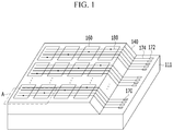
- FIG. 1 is a perspective view illustrating an organic light-emitting display device having a touch sensor according to the present invention
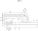
- FIG. 2 is a cross-sectional view illustrating the organic light-emitting display device having a touch sensor illustrated in FIG. 1 .
- the organic light-emitting display device having a touch sensor illustrated in FIGs. 1 and 2 includes a plurality of subpixels arranged in a matrix form on a substrate 111, an encapsulation unit 140 disposed on the subpixels, a touch electrode 160 disposed on the encapsulation unit 140, and a shield electrode 150 disposed between the encapsulation unit 140 and the touch electrode 160.
- the organic light-emitting display device having a touch sensor comprises an active area disposed on the substrate 111 and a non-active area disposed adjacent to the active area.
- the substrate 111 is formed of a flexible material such as plastic or glass so as to be foldable or bendable.
- the substrate 111 is formed of polyimide (PI), polyethylene terephthalate (PET), polyethylene naphthalate (PEN), polycarbonate (PC), polyethersulfone (PES), polyacrylate (PAR), polysulfone (PSF), or cyclic-olefin copolymer (COC).
- the active area displays an image through unit pixels arranged in a matrix form.
- Each unit pixel includes red, green and blue subpixels, or includes red, green, blue, and white subpixels.
- Each of the subpixels includes, as illustrated in FIGs. 1 and 2 , a pixel-driving circuit, including a plurality of thin-film transistors 130, and a light-emitting element 120 connected to the pixel-driving circuit.
- Each of the driving thin-film transistors 130 included in the pixel-driving circuit controls the current supplied from a high-voltage supply line to the light-emitting element 120 in response to a data signal supplied to a gate electrode of the corresponding driving thin-film transistor 130, thus adjusting the amount of light emitted from the light-emitting element 120.
- Such a driving thin-film transistor 130 includes a semiconductor layer 134 disposed on a buffer layer 104, a gate electrode 132 overlapping the semiconductor layer 134 with a gate insulation film 102 interposed therebetween, and source and drain electrodes 136 and 138 formed on an interlayer insulation film 114 so as to come into contact with the semiconductor layer 134.
- the semiconductor layer 134 is formed of at least one of an amorphous semiconductor material, a polycrystalline semiconductor material, or an oxide semiconductor material.
- the light-emitting element 120 includes an anode 122, at least one light-emitting stack 124 formed on the anode 122, and a cathode 126 formed on the light-emitting stack 124.
- the anode 122 is electrically connected to the drain electrode 138 of the driving thin-film transistor 130, which is exposed through a pixel contact hole penetrating a protective film 116 and a pixel planarization layer 118.
- the light-emitting stack 124 is formed on the anode 122 in a light-emitting area that is defined by a bank 128.
- the light-emitting stack 124 is formed by stacking a hole-related layer, an organic emission layer, and an electron-related layer on the anode 122 in that order or in the reverse order.
- the light-emitting stack 124 may include first and second light-emitting stacks, which face each other with a charge generation layer interposed therebetween.
- the organic emission layer of any one of the first and second light-emitting stacks generates blue light
- the organic emission layer of the other one of the first and second light-emitting stacks generates yellow-green light, whereby white light is generated via the first and second light-emitting stacks.
- white light generated in the light-emitting stack 124 is incident on a color filter located above or under the light-emitting stack 124, a color image may be realized.
- colored light corresponding to each subpixel may be generated in each light-emitting stack 124 in order to realize a color image without a separate color filter. That is, the light-emitting stack 124 of the red subpixel may generate red light, the light-emitting stack 124 of the green subpixel may generate green light, and the light-emitting stack 124 of the blue subpixel may generate blue light.
- the cathode 126 is formed so as to face the anode 122 with the light-emitting stack 124 interposed therebetween and is connected to a low-voltage supply line.
- the encapsulation unit 140 prevents external moisture or oxygen from permeating the light-emitting element 120, which is vulnerable to external moisture or oxygen.
- the encapsulation unit 140 includes at least one inorganic encapsulation layer 142 and at least one organic encapsulation layer 144.
- the structure of the encapsulation unit 140 in which the first inorganic encapsulation layer 142, the organic encapsulation layer 144 and the second inorganic encapsulation layer 146 are stacked in that order will be described by way of example.
- the first inorganic encapsulation layer 142 is formed on the substrate 111, on which the cathode 126 has been formed.
- the second inorganic encapsulation layer 146 is formed on the substrate 111, on which the organic encapsulation layer 144 has been formed, so as to cover the upper surface, the lower surface and the side surface of the organic encapsulation layer 144 together with the first inorganic encapsulation layer 142.
- the first and second inorganic encapsulation layers 142 and 146 minimize or prevent the permeation of external moisture or oxygen into the light-emitting stack 124.
- Each of the first and second inorganic encapsulation layers 142 and 146 is formed of an inorganic insulation material that is capable of being deposited at a low temperature, such as silicon nitride (SiNx), silicon oxide (SiOx), silicon oxide nitride (SiON), or aluminum oxide (Al 2 O 3 ).
- first and second inorganic encapsulation layers 142 and 146 are deposited in a low-temperature atmosphere, it is possible to prevent damage to the light-emitting stack 124, which is vulnerable to a high-temperature atmosphere, during the process of depositing the first and second inorganic encapsulation layers 142 and 146.
- the organic encapsulation layer 144 serves to dampen the stress between the respective layers due to bending of the organic light-emitting display device and to increase planarization performance.
- the organic encapsulation layer 144 is formed on the substrate 111, on which the first inorganic encapsulation layer 142 has been formed, using a non-photosensitive organic insulation material, such as PCL, acrylic resin, epoxy resin, polyimide, polyethylene or silicon oxycarbide (SiOC), or using a photosensitive organic insulation material such as photoacryl.
- a non-photosensitive organic insulation material such as PCL, acrylic resin, epoxy resin, polyimide, polyethylene or silicon oxycarbide (SiOC)
- a photosensitive organic insulation material such as photoacryl.
- the organic encapsulation layer 144 is disposed in the active area, rather than the non-active area.
- a plurality of touch electrodes 160 is disposed above the active area of the encapsulation unit 140. Since each of the touch electrodes 160 includes a capacitance array formed in the corresponding touch electrode 160 itself, the touch sensor may be used as a self-capacitance-type touch sensor that senses variation in capacitance due to a user touch.
- this self-capacitance sensing method using the touch electrodes 160 when a driving signal supplied through the touch pad 170 is applied to the touch electrodes 160 through routing lines 180, electric charges Q are accumulated in the touch sensor.
- parasitic capacitance is also sensed by a self-capacitance sensor, whereby a capacitance value varies. Therefore, it is possible to determine the presence or absence of a touch based on variation in the capacitance value between the touch sensor that is touched by the finger and the touch sensor that is not touched by the finger.
- the touch electrodes 160 are configured as individual pieces that are divided in first and second directions that intersect each other.
- Each of the touch electrodes 160 is formed to have a size corresponding to a plurality of subpixels in consideration of a touch area of a user.
- one touch electrode 160 has a size that is from several times to several hundred times larger than the size of one subpixel.
- Each of the touch electrodes 160 is formed in a single-layer or multi-layer structure using a transparent conductive film formed of ITO, IZO, IGZO, or ZnO or using an opaque conductive film formed of opaque metal having high corrosion resistance and acid resistance and excellent conductivity, such as, for example, Ta, Ti, Cu, or Mo.
- the touch electrodes 160 are formed of opaque metal, the touch electrodes 160 are formed in a mesh shape that does not overlap the emission area but overlaps the bank 128, thereby preventing an aperture ratio and transmissivity from being lowered by the touch electrodes 160. Since the mesh-shaped touch electrodes 160 have higher conductivity than a transparent conductive film, the touch electrodes 160 may be configured as low-resistance electrodes. Thereby, the resistance and capacitance of the touch electrodes 160 may be reduced, and the RC time constant may be reduced, which may result in increased touch sensitivity.
- Each of the routing lines 180 which is connected to a respective one of the touch electrodes 160 in a one-to-one correspondence manner, is formed in any one of a first direction and a second direction.
- the first direction may be a vertical direction
- the second direction may be a horizontal direction perpendicular to the vertical direction.
- the routing lines 180 which cross the touch electrodes 160, are disposed so as to overlap the bank 128, thereby preventing the aperture ratio from being lowered by the routing lines 180.
- the routing lines 180 are disposed on the upper surface and the side surface of the second inorganic encapsulation layer 146, which is the uppermost layer of the encapsulation unit 140.
- the routing lines 180 even when external oxygen or moisture permeates through the routing lines 180, the oxygen or moisture is blocked by the organic encapsulation layer 144 and the first and second inorganic encapsulation layers 142 and 146, thereby protecting the light-emitting stack 124 from the oxygen or moisture.
- each of the routing lines 180 includes first and second routing lines 182 and 184, which are electrically connected to each other via routing contact holes 166.
- a portion of the touch insulation film 156 and the second routing lines 184 are both disposed on the side surface of the encapsulation unit 140 and extend to a pad area of the display device.
- the touch insulation film 156 serves to protect the second routing lines 184 on the side surface from external moisture or oxygen, for example, due to the touch insulation film 156 covering the second routing lines 184 on the side surface, as shown in FIG.2 .
- the first routing lines 182 and the touch electrode 160 are on a same plane or layer, and the second routing lines 184 and the shield electrode 150 are formed on a same plane or layer.
- the first routing lines 182 and the touch electrode 160 are formed as part of the same layer, and the second routing lines 184 and the shield electrode 150 are also formed as part of the same layer.
- the touch electrode 160 and the first routing lines 182 are disposed in contact with the touch insulation film 156, and the second routing lines 184 and the shield electrode 150 are disposed in contact with the inorganic encapsulation layer 146.
- a plurality of first routing lines 182 is disposed so as to be spaced apart from each other in a longitudinal (length) direction of each routing line 180.
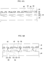
- Each of the first routing lines 182, as illustrated in FIGs. 5A and 6A is formed of the same material as the touch electrodes 160 on a touch insulation film 156, and is coplanar with the touch electrodes 160.
- the first routing lines 182, which are formed so as to be surrounded by the touch electrodes 160 are disposed so as to be spaced apart from the touch electrodes 160, with a first separation hole 162 therebetween.
- the first separation hole 162 may be formed around substantially all or at least some of the perimeter of a first routing line 182, as shown in FIG. 5A for example.
- a first routing line 182 which is connected to the k th touch electrode 160 is directly connected to the corresponding touch electrode 160 without a separate contact hole, as illustrated by the top middle first routing line 182 in FIG. 5A .
- a first routing line 182, which is not directly connected to the k th touch electrode 160, is disposed so as to be spaced apart from the corresponding touch electrode 160, with the first separation hole 162 therebetween, as illustrated in the top leftmost and top rightmost first separation holes 162 of FIG. 5A .
- Each of the second routing lines 184 is formed of the same material as the shield electrode 150 on the second inorganic encapsulation layer 146, and is coplanar with the shield electrode 150.
- the second routing lines 184 which are formed so as to be surrounded by the shield electrode 150, are disposed so as to be spaced apart from the shield electrode 150, with a second separation hole 152 therebetween.
- the second separation hole 152 may be formed around substantially all or at least some of the perimeter of a second routing line 184, as shown in FIG. 5B for example.
- each of the second routing lines 184 is disposed between two adjacent ones of the first routing lines 182 (see FIG. 6C in particular). As illustrated in FIGs. 6B and 6C , each of the second routing lines 184 is exposed through the routing contact holes 166 penetrating the touch insulation film 156, and is electrically connected to the first routing lines 182.
- each one of the first routing lines 182 is formed in the region corresponding to a respective one of the touch electrodes 160 so as to overlap the shield electrode 150.
- each of the second routing lines 184 is formed between two adjacent ones of the touch electrodes 160 while overlapping two different touch electrodes 160 that are disposed adjacent thereto in the vertical (longitudinal, length) direction.
- two routing contact holes 166 are disposed in the regions in which each routing line 180 corresponds to a respective one of the touch electrodes 160.
- a first contact hole 166 is disposed in a first region in which a first routing line 182 and a second routing line 184 overlap
- a second contact hole 166 is disposed in a second region in which a different first routing line 182 and the same second routing line 184 overlap, as shown in FIG. 3 .
- the second routing line 184 corresponds to two different touch electrodes 160 and overlaps two different first routing lines 182.
- the first and second routing lines 182 and 184 are electrically connected to each other via two routing contact holes 166 in the regions corresponding to a respective one of the touch electrodes 160.
- the second routing lines 184 are disposed not only between two adjacent ones of the touch electrodes 160 but also between the at least two first routing lines 182 in the region corresponding to a respective one of the touch electrodes 160.
- a second routing line 184 may be disposed between two different first routing lines 182 on the same touch electrode 160.
- at least four routing contact holes 166 are disposed in the regions in which each routing line 180 corresponds to a respective one of the touch electrodes 160.
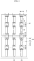
- the number of routing contact holes 166 used for the connection of the first and second routing lines 182 and 184 in the configuration illustrated in FIG. 4 is greater than the number of routing contact holes 166 in the configuration illustrated in FIG. 3 , it is possible to prevent defective contact between the first and second routing lines 182 and 184.
- the greater the number of routing contact holes 166 the greater the contact area.
- the electrical contact between the first and second routing lines 182 and 184 has increased stability due to the increased number of routing contact holes 166.
- the shield electrode 150 is disposed on the second inorganic encapsulation layer 146, which is formed between the touch electrodes 160 and the cathode 126 of the light-emitting element 126.
- the shield electrode 150 is formed on the entire surface of the active area so as to overlap the touch electrodes 160, with the touch insulation film 156 interposed therebetween.
- the shield electrode 150 is formed in a single-layer or multi-layer structure using a transparent conductive film formed of ITO, IZO, IGZO, or ZnO or using an opaque conductive film formed of metal having high corrosion resistance and acid resistance and excellent conductivity, such as, for example, Ta, Ti, Cu, or Mo, or is formed in a multi-layer structure in which the transparent conductive film 151a and the opaque conductive film 151b are stacked in that order or in the reverse order.
- the shield electrode 150 includes the opaque conductive film, the shield electrode 150 is formed in a mesh shape that does not overlap the emission area but overlaps the bank 128, thereby preventing an aperture ratio and transmissivity from being lowered by the shield electrode 150.
- a load free driving signal LFD which is an alternating-current signal of a voltage having at least one of an amplitude or phase the same as that of the touch-driving signal, is supplied to the shield electrode 150.
- LFD alternating-current signal of a voltage having at least one of an amplitude or phase the same as that of the touch-driving signal
- a touch pad 170 and a shield pad 172 are disposed in the pad area of the substrate 111 that is exposed by, and not covered by, the encapsulation unit 140.
- the pad area, in which the touch pad 170 and the shield pad 172 are disposed, may be bent and disposed on the rear surface of the active area AA.
- the area occupied by the active area is maximized and the area corresponding to the pad area is minimized on the entire screen of the display device.
- the touch pad 170 and the shield pad 172 are disposed in the same plane as a display pad (not illustrated), which is connected to at least one of a scan line or a data line of the pixel-driving circuit.
- each of the touch pad 170, the shield pad 172 and the display pad is disposed on at least one display insulation film of the buffer layer 104, the interlayer insulation film 114, or the planarization film 118, which is disposed between the substrate 111 and the encapsulation unit 140, or on the touch insulation film 156.
- the touch pad 170, the shield pad 172 and the display pad are formed so as to be exposed by, and not covered by, a touch protective film 158, and are thus connected to a signal transmission film, on which a touch-driving circuit (not illustrated) is installed.
- the touch protective film 158 is formed to cover the touch electrodes 160, thus preventing the touch electrodes 160 from corroding due to external moisture or the like.
- the touch protective film 158 is formed in a film or thin-film configuration using an organic insulation material such as epoxy or acryl or using an inorganic insulation material such as SiNx or SiOx.
- the touch pad 170 supplies a touch-driving signal to the touch electrodes 160 via the routing lines 180.
- the touch pad 170 receives a touch-driving signal, sensed by the touch electrodes 160, via the routing lines 180, and supplies the touch-driving signal to the touch-driving circuit (not illustrated), which is connected with the touch pad 170.
- the touch-driving circuit determines the presence or absence of a user touch and a touch position by sensing variation in capacitance, which is changed due to a user touch.
- the shield pad 172 is formed in a single-layer or multi-layer structure using metal having high corrosion resistance and acid resistance and excellent conductivity, such as, for example, Ta, Ti, Cu, or Mo.
- the touch pad 170 is formed in a multi-layer structure, such as Ti/Al/Ti or Mo/Al/Mo, in which metal having high corrosion resistance and acid resistance is disposed at the uppermost layer.
- the shield pad 172 is connected to the shield electrode 150 via a shield line 174, which is formed along the side surface of the encapsulation unit 140 as shown in FIG. 1 .
- the shield pad 172 supplies a load free driving signal LFD, at least one of the amplitude or the phase of which is the same as that of the touch-driving signal, to the shield line 174.
- LFD load free driving signal
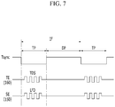
- FIG. 7 is a waveform diagram illustrating the signal waveform to be supplied to the touch electrodes and the shield electrode in the display device having a touch sensor according to the present invention.
- one frame period 1F is time-divided into a display period DP and a touch-sensing period TP.
- One touch-sensing period TP is allocated between the display periods DP.
- a pixel-driving signal (e.g. a scan signal, a data signal, a low-voltage driving signal, and a high-voltage driving signal) is supplied to each subpixel.
- the scan signal is the voltage of a gate pulse to be supplied to each scan line.
- the data signal is the data voltage of an input image to be supplied to each data line during the display period.
- the low-voltage driving signal is the voltage to be supplied to the cathode of each light-emitting element 120 during the display period DP.
- the high-voltage driving signal is the voltage to be supplied to the drain electrode of each driving transistor during the display period DP.
- the touch electrodes TE or 160 may be switched to a floating state in which no signal is applied thereto or to a state in which a specific voltage (e.g. ground voltage) is applied thereto.
- the touch-driving circuit supplies a touch-driving signal TDS to the touch electrodes TE or 160, and supplies a load free driving signal LFD, which has the same phase and amplitude as the touch-driving signal TDS to be supplied to the touch electrodes TE or 160, to the shield electrode SE or 150.
- a touch control signal Tsync from a timing controller
- the touch-driving circuit supplies a touch-driving signal TDS to the touch electrodes TE or 160, and supplies a load free driving signal LFD, which has the same phase and amplitude as the touch-driving signal TDS to be supplied to the touch electrodes TE or 160, to the shield electrode SE or 150.
- the light-emitting element 120 and the pixel-driving circuit are not illustrated in FIGs. 6A to 6D , a plurality of light-emitting elements 120 and pixel-driving circuits may be disposed under the encapsulation unit 140, as illustrated in FIG. 2 .
- a shield electrode is disposed between a light-emitting element and touch electrodes. While a touch-driving signal is applied to the touch electrodes, a load free driving signal of which at least one of the phase or the amplitude is the same as that of the touch-driving signal is supplied to the shield electrode. As a result, it is possible to remove touch noise and consequently to secure improved touch-sensing performance.
Landscapes
- Engineering & Computer Science (AREA)
- General Engineering & Computer Science (AREA)
- Theoretical Computer Science (AREA)
- Human Computer Interaction (AREA)
- Physics & Mathematics (AREA)
- General Physics & Mathematics (AREA)
- Computer Networks & Wireless Communication (AREA)
- Microelectronics & Electronic Packaging (AREA)
- Electroluminescent Light Sources (AREA)
Abstract
Description
- This application claims the benefit of Korean Patent Application No.
2018-0084292, filed on July 19, 2018 - The present invention relates to a display device, and more particularly to a display device having a touch sensor for securing improved touch-sensing performance.
- A touch sensor is an input device through which a user may input a command by selecting instructions displayed on a screen of a display device using a hand or an object. That is, the touch sensor converts a contact position that directly contacts a human hand or an object into an electrical signal and receives selected instructions based on the contact position as an input signal. Such a touch sensor may substitute for a separate input device that is connected to a display device and operated, such as a keyboard or a mouse, and thus the range of application of the touch sensor has continually increased.
- In the case in which a touch sensor is disposed on a display device, parasitic capacitance is formed at a region at which the conductive layers of the display device and the touch sensor overlap each other. This parasitic capacitance increases a touch-driving load and deteriorates touch-sensing accuracy. In particular, the shorter the distance between the conductive layer of the display device and the touch sensor, the larger the parasitic capacitance, which makes it difficult to ensure touch-sensing performance.
- An invention is defined in the independent claim. Accordingly, the present invention is directed to a display device having a touch sensor that substantially obviates one or more problems due to limitations and disadvantages of the related art.
- An object of the present invention is to provide a display device having a touch sensor for securing improved touch-sensing performance.
- Additional advantages, objects, and features of the invention will be set forth in part in the description which follows and in part will become apparent to those having ordinary skill in the art upon examination of the following or may be learned from practice of the invention. The objectives and other advantages of the invention may be realized and attained by the structure particularly pointed out in the written description and claims hereof as well as the appended drawings.
- To achieve these objects and other advantages and in accordance with the purpose of the invention, as embodied and broadly described herein, a display device having a touch sensor includes a shield electrode and a touch electrode, which are sequentially disposed on an encapsulation unit covering a light-emitting element. While a touch-driving signal is applied to the touch electrode, a load free driving signal of which at least one of the phase or the amplitude is the same as that of the touch-driving signal is supplied to the shield electrode, thereby securing improved touch-sensing performance.
- It is to be understood that both the foregoing general description and the following detailed description of the present invention are exemplary and explanatory and are intended to provide further explanation of the invention as claimed.
- The accompanying drawings, which are included to provide a further understanding of the invention and are incorporated in and constitute a part of this application, illustrate embodiment(s) of the invention and together with the description serve to explain the principle of the invention. In the drawings:
-
FIG. 1 is a perspective view illustrating a display panel having a touch sensor according to an example; -
FIG. 2 is a cross-sectional view illustrating the display device having a touch sensor illustrated inFIG. 1 in detail; -
FIG. 3 is a plan view illustrating region A illustrated inFIG. 1 in detail; -
FIG. 4 is a plan view illustrating another example of region A illustrated inFIG. 1 in detail; -
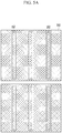
FIG. 5A is a plan view illustrating the arrangement relationship between a touch electrode and a first routing line illustrated inFIG. 3 , andFIG. 5B is a plan view illustrating the arrangement relationship between a shield electrode and a second routing line illustrated inFIG. 3 ; -
FIG. 6A is a cross-sectional view taken along line I-I' in the display device having a touch sensor illustrated inFIGs. 3 and4 ,FIG. 6B is a cross-sectional view taken along line II-II' in the display device having a touch sensor illustrated inFIGs. 3 and4 ,FIG. 6C is a cross-sectional view taken along line III-III' in the display device having a touch sensor illustrated inFIGs. 3 and4 , andFIG. 6D is a cross-sectional view taken along line IV-IV' in the display device having a touch sensor illustrated inFIG. 4 ; and -
FIG. 7 is a waveform diagram illustrating the signal waveform to be supplied to a touch electrode and a shield electrode in the display device having a touch sensor according to an example. - Reference will now be made in detail to exemplary embodiments of the present invention, examples of which are illustrated in the accompanying drawings. Wherever possible, the same reference numbers will be used throughout the drawings to refer to the same or like parts.
-
FIG. 1 is a perspective view illustrating an organic light-emitting display device having a touch sensor according to the present invention, andFIG. 2 is a cross-sectional view illustrating the organic light-emitting display device having a touch sensor illustrated inFIG. 1 . - The organic light-emitting display device having a touch sensor illustrated in
FIGs. 1 and2 includes a plurality of subpixels arranged in a matrix form on asubstrate 111, anencapsulation unit 140 disposed on the subpixels, atouch electrode 160 disposed on theencapsulation unit 140, and ashield electrode 150 disposed between theencapsulation unit 140 and thetouch electrode 160. - The organic light-emitting display device having a touch sensor comprises an active area disposed on the
substrate 111 and a non-active area disposed adjacent to the active area. Thesubstrate 111 is formed of a flexible material such as plastic or glass so as to be foldable or bendable. For example, thesubstrate 111 is formed of polyimide (PI), polyethylene terephthalate (PET), polyethylene naphthalate (PEN), polycarbonate (PC), polyethersulfone (PES), polyacrylate (PAR), polysulfone (PSF), or cyclic-olefin copolymer (COC). - The active area displays an image through unit pixels arranged in a matrix form. Each unit pixel includes red, green and blue subpixels, or includes red, green, blue, and white subpixels.
- Each of the subpixels includes, as illustrated in
FIGs. 1 and2 , a pixel-driving circuit, including a plurality of thin-film transistors 130, and a light-emitting element 120 connected to the pixel-driving circuit. - Each of the driving thin-
film transistors 130 included in the pixel-driving circuit controls the current supplied from a high-voltage supply line to the light-emitting element 120 in response to a data signal supplied to a gate electrode of the corresponding driving thin-film transistor 130, thus adjusting the amount of light emitted from the light-emitting element 120. - Such a driving thin-
film transistor 130, as illustrated inFIG. 2 , includes asemiconductor layer 134 disposed on abuffer layer 104, agate electrode 132 overlapping thesemiconductor layer 134 with agate insulation film 102 interposed therebetween, and source anddrain electrodes interlayer insulation film 114 so as to come into contact with thesemiconductor layer 134. Here, thesemiconductor layer 134 is formed of at least one of an amorphous semiconductor material, a polycrystalline semiconductor material, or an oxide semiconductor material. - The light-emitting element 120 includes an
anode 122, at least one light-emitting stack 124 formed on theanode 122, and acathode 126 formed on the light-emitting stack 124. - The
anode 122 is electrically connected to thedrain electrode 138 of the driving thin-film transistor 130, which is exposed through a pixel contact hole penetrating aprotective film 116 and apixel planarization layer 118. - The light-emitting stack 124 is formed on the
anode 122 in a light-emitting area that is defined by abank 128. The light-emitting stack 124 is formed by stacking a hole-related layer, an organic emission layer, and an electron-related layer on theanode 122 in that order or in the reverse order. In addition, the light-emitting stack 124 may include first and second light-emitting stacks, which face each other with a charge generation layer interposed therebetween. In this case, the organic emission layer of any one of the first and second light-emitting stacks generates blue light, and the organic emission layer of the other one of the first and second light-emitting stacks generates yellow-green light, whereby white light is generated via the first and second light-emitting stacks. Since the white light generated in the light-emitting stack 124 is incident on a color filter located above or under the light-emitting stack 124, a color image may be realized. In addition, colored light corresponding to each subpixel may be generated in each light-emitting stack 124 in order to realize a color image without a separate color filter. That is, the light-emitting stack 124 of the red subpixel may generate red light, the light-emitting stack 124 of the green subpixel may generate green light, and the light-emitting stack 124 of the blue subpixel may generate blue light. - The
cathode 126 is formed so as to face theanode 122 with the light-emitting stack 124 interposed therebetween and is connected to a low-voltage supply line. - The
encapsulation unit 140 prevents external moisture or oxygen from permeating the light-emitting element 120, which is vulnerable to external moisture or oxygen. To this end, theencapsulation unit 140 includes at least oneinorganic encapsulation layer 142 and at least oneorganic encapsulation layer 144. In the present invention, the structure of theencapsulation unit 140 in which the firstinorganic encapsulation layer 142, theorganic encapsulation layer 144 and the second inorganic encapsulation layer 146 are stacked in that order will be described by way of example. - The first
inorganic encapsulation layer 142 is formed on thesubstrate 111, on which thecathode 126 has been formed. The second inorganic encapsulation layer 146 is formed on thesubstrate 111, on which theorganic encapsulation layer 144 has been formed, so as to cover the upper surface, the lower surface and the side surface of theorganic encapsulation layer 144 together with the firstinorganic encapsulation layer 142. - The first and second
inorganic encapsulation layers 142 and 146 minimize or prevent the permeation of external moisture or oxygen into the light-emitting stack 124. Each of the first and second inorganic encapsulation layers 142 and 146 is formed of an inorganic insulation material that is capable of being deposited at a low temperature, such as silicon nitride (SiNx), silicon oxide (SiOx), silicon oxide nitride (SiON), or aluminum oxide (Al2O3). Thus, since the first and second inorganic encapsulation layers 142 and 146 are deposited in a low-temperature atmosphere, it is possible to prevent damage to the light-emitting stack 124, which is vulnerable to a high-temperature atmosphere, during the process of depositing the first and second inorganic encapsulation layers 142 and 146. - The
organic encapsulation layer 144 serves to dampen the stress between the respective layers due to bending of the organic light-emitting display device and to increase planarization performance. Theorganic encapsulation layer 144 is formed on thesubstrate 111, on which the firstinorganic encapsulation layer 142 has been formed, using a non-photosensitive organic insulation material, such as PCL, acrylic resin, epoxy resin, polyimide, polyethylene or silicon oxycarbide (SiOC), or using a photosensitive organic insulation material such as photoacryl. Theorganic encapsulation layer 144 is disposed in the active area, rather than the non-active area. - A plurality of
touch electrodes 160 is disposed above the active area of theencapsulation unit 140. Since each of thetouch electrodes 160 includes a capacitance array formed in thecorresponding touch electrode 160 itself, the touch sensor may be used as a self-capacitance-type touch sensor that senses variation in capacitance due to a user touch. In this self-capacitance sensing method using thetouch electrodes 160, when a driving signal supplied through thetouch pad 170 is applied to thetouch electrodes 160 throughrouting lines 180, electric charges Q are accumulated in the touch sensor. At this time, when a user's finger or a conductive object touches thetouch electrodes 160, parasitic capacitance is also sensed by a self-capacitance sensor, whereby a capacitance value varies. Therefore, it is possible to determine the presence or absence of a touch based on variation in the capacitance value between the touch sensor that is touched by the finger and the touch sensor that is not touched by the finger. - To this end, the
touch electrodes 160 are configured as individual pieces that are divided in first and second directions that intersect each other. Each of thetouch electrodes 160 is formed to have a size corresponding to a plurality of subpixels in consideration of a touch area of a user. For example, onetouch electrode 160 has a size that is from several times to several hundred times larger than the size of one subpixel. - Each of the
touch electrodes 160 is formed in a single-layer or multi-layer structure using a transparent conductive film formed of ITO, IZO, IGZO, or ZnO or using an opaque conductive film formed of opaque metal having high corrosion resistance and acid resistance and excellent conductivity, such as, for example, Ta, Ti, Cu, or Mo. When thetouch electrodes 160 are formed of opaque metal, thetouch electrodes 160 are formed in a mesh shape that does not overlap the emission area but overlaps thebank 128, thereby preventing an aperture ratio and transmissivity from being lowered by thetouch electrodes 160. Since the mesh-shapedtouch electrodes 160 have higher conductivity than a transparent conductive film, thetouch electrodes 160 may be configured as low-resistance electrodes. Thereby, the resistance and capacitance of thetouch electrodes 160 may be reduced, and the RC time constant may be reduced, which may result in increased touch sensitivity. - Each of the
routing lines 180, which is connected to a respective one of thetouch electrodes 160 in a one-to-one correspondence manner, is formed in any one of a first direction and a second direction. The first direction may be a vertical direction, and the second direction may be a horizontal direction perpendicular to the vertical direction. - In the active area, the
routing lines 180, which cross thetouch electrodes 160, are disposed so as to overlap thebank 128, thereby preventing the aperture ratio from being lowered by the routing lines 180. - In the non-active area, the
routing lines 180 are disposed on the upper surface and the side surface of the second inorganic encapsulation layer 146, which is the uppermost layer of theencapsulation unit 140. Thus, even when external oxygen or moisture permeates through therouting lines 180, the oxygen or moisture is blocked by theorganic encapsulation layer 144 and the first and second inorganic encapsulation layers 142 and 146, thereby protecting the light-emitting stack 124 from the oxygen or moisture. - As illustrated in
FIGs. 3 and4 , each of therouting lines 180 includes first andsecond routing lines FIG. 2 , a portion of thetouch insulation film 156 and thesecond routing lines 184 are both disposed on the side surface of theencapsulation unit 140 and extend to a pad area of the display device. Thetouch insulation film 156 serves to protect thesecond routing lines 184 on the side surface from external moisture or oxygen, for example, due to thetouch insulation film 156 covering thesecond routing lines 184 on the side surface, as shown inFIG.2 . - As shown in
FIG. 2 , thefirst routing lines 182 and thetouch electrode 160 are on a same plane or layer, and thesecond routing lines 184 and theshield electrode 150 are formed on a same plane or layer. In other words, thefirst routing lines 182 and thetouch electrode 160 are formed as part of the same layer, and thesecond routing lines 184 and theshield electrode 150 are also formed as part of the same layer. Thetouch electrode 160 and thefirst routing lines 182 are disposed in contact with thetouch insulation film 156, and thesecond routing lines 184 and theshield electrode 150 are disposed in contact with the inorganic encapsulation layer 146. - A plurality of
first routing lines 182 is disposed so as to be spaced apart from each other in a longitudinal (length) direction of eachrouting line 180. Each of thefirst routing lines 182, as illustrated inFIGs. 5A and6A , is formed of the same material as thetouch electrodes 160 on atouch insulation film 156, and is coplanar with thetouch electrodes 160. Thus, thefirst routing lines 182, which are formed so as to be surrounded by thetouch electrodes 160, are disposed so as to be spaced apart from thetouch electrodes 160, with afirst separation hole 162 therebetween. Thefirst separation hole 162 may be formed around substantially all or at least some of the perimeter of afirst routing line 182, as shown inFIG. 5A for example. - Here, among a plurality of
routing lines 182, which extend across the kth (where k is a natural number)touch electrode 160, afirst routing line 182, which is connected to the kth touch electrode 160, is directly connected to thecorresponding touch electrode 160 without a separate contact hole, as illustrated by the top middlefirst routing line 182 inFIG. 5A . Afirst routing line 182, which is not directly connected to the kth touch electrode 160, is disposed so as to be spaced apart from thecorresponding touch electrode 160, with thefirst separation hole 162 therebetween, as illustrated in the top leftmost and top rightmost first separation holes 162 ofFIG. 5A . - Each of the
second routing lines 184, as illustrated inFIGs. 5B and6B , is formed of the same material as theshield electrode 150 on the second inorganic encapsulation layer 146, and is coplanar with theshield electrode 150. Thus, thesecond routing lines 184, which are formed so as to be surrounded by theshield electrode 150, are disposed so as to be spaced apart from theshield electrode 150, with asecond separation hole 152 therebetween. Thesecond separation hole 152 may be formed around substantially all or at least some of the perimeter of asecond routing line 184, as shown inFIG. 5B for example. - In order to connect
first routing lines 182 disposed indifferent touch electrodes 160, as illustrated inFIGs. 6B and6C , each of thesecond routing lines 184 is disposed between two adjacent ones of the first routing lines 182 (seeFIG. 6C in particular). As illustrated inFIGs. 6B and6C , each of thesecond routing lines 184 is exposed through the routing contact holes 166 penetrating thetouch insulation film 156, and is electrically connected to the first routing lines 182. - Meanwhile, in the configuration illustrated in
FIG. 3 , each one of thefirst routing lines 182 is formed in the region corresponding to a respective one of thetouch electrodes 160 so as to overlap theshield electrode 150. Thus, each of thesecond routing lines 184 is formed between two adjacent ones of thetouch electrodes 160 while overlapping twodifferent touch electrodes 160 that are disposed adjacent thereto in the vertical (longitudinal, length) direction. In this case, two routing contact holes 166 are disposed in the regions in which eachrouting line 180 corresponds to a respective one of thetouch electrodes 160. In other words, afirst contact hole 166 is disposed in a first region in which afirst routing line 182 and asecond routing line 184 overlap, and asecond contact hole 166 is disposed in a second region in which a differentfirst routing line 182 and the samesecond routing line 184 overlap, as shown inFIG. 3 . In this case, thesecond routing line 184 corresponds to twodifferent touch electrodes 160 and overlaps two different first routing lines 182. Thus, the first andsecond routing lines touch electrodes 160. - In the configuration illustrated in
FIG. 4 , at least two of thefirst routing lines 182 are formed in the region corresponding to a respective one of thetouch electrodes 160 so as to overlap theshield electrode 150. Thus, thesecond routing lines 184 are disposed not only between two adjacent ones of thetouch electrodes 160 but also between the at least twofirst routing lines 182 in the region corresponding to a respective one of thetouch electrodes 160. In other words, asecond routing line 184 may be disposed between two differentfirst routing lines 182 on thesame touch electrode 160. In this case, at least four routing contact holes 166 are disposed in the regions in which eachrouting line 180 corresponds to a respective one of thetouch electrodes 160. As such, since the number of routing contact holes 166 used for the connection of the first andsecond routing lines FIG. 4 is greater than the number of routing contact holes 166 in the configuration illustrated inFIG. 3 , it is possible to prevent defective contact between the first andsecond routing lines second routing lines - The
shield electrode 150 is disposed on the second inorganic encapsulation layer 146, which is formed between thetouch electrodes 160 and thecathode 126 of the light-emittingelement 126. Here, theshield electrode 150 is formed on the entire surface of the active area so as to overlap thetouch electrodes 160, with thetouch insulation film 156 interposed therebetween. - The
shield electrode 150 is formed in a single-layer or multi-layer structure using a transparent conductive film formed of ITO, IZO, IGZO, or ZnO or using an opaque conductive film formed of metal having high corrosion resistance and acid resistance and excellent conductivity, such as, for example, Ta, Ti, Cu, or Mo, or is formed in a multi-layer structure in which the transparentconductive film 151a and the opaqueconductive film 151b are stacked in that order or in the reverse order. When theshield electrode 150 includes the opaque conductive film, theshield electrode 150 is formed in a mesh shape that does not overlap the emission area but overlaps thebank 128, thereby preventing an aperture ratio and transmissivity from being lowered by theshield electrode 150. - During a touch-sensing period, a load free driving signal LFD, which is an alternating-current signal of a voltage having at least one of an amplitude or phase the same as that of the touch-driving signal, is supplied to the
shield electrode 150. Thus, because there is no difference in voltage between theshield electrode 150 and thetouch electrodes 160, it is possible to minimize parasitic capacitance between theshield electrode 150 and thetouch electrodes 160. In addition, theshield electrode 150 may also block noise generated by the electrodes and the signal lines of the display panel. - As illustrated in
FIGs. 1 and2 , atouch pad 170 and ashield pad 172 are disposed in the pad area of thesubstrate 111 that is exposed by, and not covered by, theencapsulation unit 140. The pad area, in which thetouch pad 170 and theshield pad 172 are disposed, may be bent and disposed on the rear surface of the active area AA. Thus, the area occupied by the active area is maximized and the area corresponding to the pad area is minimized on the entire screen of the display device. - The
touch pad 170 and theshield pad 172 are disposed in the same plane as a display pad (not illustrated), which is connected to at least one of a scan line or a data line of the pixel-driving circuit. For example, each of thetouch pad 170, theshield pad 172 and the display pad is disposed on at least one display insulation film of thebuffer layer 104, theinterlayer insulation film 114, or theplanarization film 118, which is disposed between thesubstrate 111 and theencapsulation unit 140, or on thetouch insulation film 156. - The
touch pad 170, theshield pad 172 and the display pad are formed so as to be exposed by, and not covered by, a touchprotective film 158, and are thus connected to a signal transmission film, on which a touch-driving circuit (not illustrated) is installed. The touchprotective film 158 is formed to cover thetouch electrodes 160, thus preventing thetouch electrodes 160 from corroding due to external moisture or the like. The touchprotective film 158 is formed in a film or thin-film configuration using an organic insulation material such as epoxy or acryl or using an inorganic insulation material such as SiNx or SiOx. - The
touch pad 170 supplies a touch-driving signal to thetouch electrodes 160 via the routing lines 180. In addition, thetouch pad 170 receives a touch-driving signal, sensed by thetouch electrodes 160, via therouting lines 180, and supplies the touch-driving signal to the touch-driving circuit (not illustrated), which is connected with thetouch pad 170. The touch-driving circuit determines the presence or absence of a user touch and a touch position by sensing variation in capacitance, which is changed due to a user touch. - Like the
touch pad 170, theshield pad 172 is formed in a single-layer or multi-layer structure using metal having high corrosion resistance and acid resistance and excellent conductivity, such as, for example, Ta, Ti, Cu, or Mo. For example, thetouch pad 170 is formed in a multi-layer structure, such as Ti/Al/Ti or Mo/Al/Mo, in which metal having high corrosion resistance and acid resistance is disposed at the uppermost layer. - The
shield pad 172 is connected to theshield electrode 150 via ashield line 174, which is formed along the side surface of theencapsulation unit 140 as shown inFIG. 1 . Thus, during a touch-sensing period, theshield pad 172 supplies a load free driving signal LFD, at least one of the amplitude or the phase of which is the same as that of the touch-driving signal, to theshield line 174. Thus, there is no difference in voltage between theshield electrode 150 and thetouch electrodes 160 during a touch-sensing period, and thus it is possible to minimize parasitic capacitance between theshield electrode 150 and thetouch electrodes 160, thereby blocking noise that may be generated during a touch-sensing period. -
FIG. 7 is a waveform diagram illustrating the signal waveform to be supplied to the touch electrodes and the shield electrode in the display device having a touch sensor according to the present invention. - Referring to
FIG. 7 , one frame period 1F is time-divided into a display period DP and a touch-sensing period TP. One touch-sensing period TP is allocated between the display periods DP. - During the display period DP, a pixel-driving signal (e.g. a scan signal, a data signal, a low-voltage driving signal, and a high-voltage driving signal) is supplied to each subpixel. Here, the scan signal is the voltage of a gate pulse to be supplied to each scan line. The data signal is the data voltage of an input image to be supplied to each data line during the display period. The low-voltage driving signal is the voltage to be supplied to the cathode of each light-emitting element 120 during the display period DP. The high-voltage driving signal is the voltage to be supplied to the drain electrode of each driving transistor during the display period DP. During the display period DP, the touch electrodes TE or 160 may be switched to a floating state in which no signal is applied thereto or to a state in which a specific voltage (e.g. ground voltage) is applied thereto.
- During the touch-sensing period TP, in response to a touch control signal Tsync from a timing controller, the touch-driving circuit supplies a touch-driving signal TDS to the touch electrodes TE or 160, and supplies a load free driving signal LFD, which has the same phase and amplitude as the touch-driving signal TDS to be supplied to the touch electrodes TE or 160, to the shield electrode SE or 150. Thus, it is possible to minimize parasitic capacitance between the touch electrodes TE or 160 and the subpixels, thereby removing touch noise and consequently increasing touch-sensing accuracy.
- Although the light-emitting element 120 and the pixel-driving circuit are not illustrated in
FIGs. 6A to 6D , a plurality of light-emitting elements 120 and pixel-driving circuits may be disposed under theencapsulation unit 140, as illustrated inFIG. 2 . - As is apparent from the above description, according to the present invention, a shield electrode is disposed between a light-emitting element and touch electrodes. While a touch-driving signal is applied to the touch electrodes, a load free driving signal of which at least one of the phase or the amplitude is the same as that of the touch-driving signal is supplied to the shield electrode. As a result, it is possible to remove touch noise and consequently to secure improved touch-sensing performance.
- It will be apparent to those skilled in the art that various modifications and variations can be made in the present invention without departing from the scope of the invention. Thus, it is intended that the present invention covers the modifications and variations of this invention provided they come within the scope of the appended claims.
- Also disclosed herein are the following numbered clauses:
- 1. A display device having a touch sensor, comprising:
- a light-emitting element disposed on a substrate;
- an encapsulation unit disposed on the light-emitting element;
- a plurality of touch electrodes disposed on the encapsulation unit; and
- a shield electrode disposed between the light-emitting element and the touch electrodes,
- wherein, while a touch-driving signal is applied to the touch electrodes, a load free driving signal of which at least one of a phase or an amplitude is same as a phase or an amplitude of the touch-driving signal is supplied to the shield electrode.
- 2. The display device according to clause 1, wherein the shield electrode is disposed on the encapsulation unit, and
wherein each of the touch electrodes has a touch sensor overlapping the shield electrode, with a touch insulation film interposed therebetween. - 3. The display device according to clause 1 or 2, further comprising:
a plurality of routing lines, each of the routing lines being connected to a respective one of the touch electrodes. - 4. The display device according to clause 3, wherein the routing lines are disposed along a side surface of the encapsulation unit.
- 5. The display device according to clause 3 or 4, wherein each of the routing lines comprises:
- first routing lines spaced apart from each other in a longitudinal direction of each of the routing lines; and
- second routing lines disposed between the first routing lines, the second routing lines electrically connecting the first routing lines to each other.
- 6. The display device according to clause 5, wherein the first routing lines are spaced apart from the touch electrodes, with first separation holes therebetween, in a same plane as the touch electrodes, and
wherein the second routing lines are spaced apart from the shield electrode, with second separation holes therebetween, in a same plane as the shield electrode. - 7. The display device according to clause 5 or 6, wherein the first routing lines are surrounded by the touch electrodes, and
wherein the second routing lines are surround by the shield electrode. - 8. The display device according any of clauses 5 to 7, wherein at least one of the first routing lines is formed in a region corresponding to a respective one of the touch electrodes.
- 9. The display device according to any of clauses 5 to 8, wherein the second routing lines are disposed between the touch electrodes.
- 10. The display device according to any of claims 5 to 8, wherein the second routing lines are disposed between the touch electrodes and between at least two of the first routing lines formed in the region corresponding to a respective one of the touch electrodes.
- 11. The display device according to any of clauses 3 to 10, further comprising:
- a shield line disposed along a side surface of the encapsulation unit, the shield line being connected to the shield electrode;
- a shield pad connected to the shield line, the shield pad being disposed on a portion of the substrate that is exposed by the encapsulation unit; and
- a touch pad connected to the routing lines, the touch pad being disposed adjacent to the shield pad.
- 12. The display device according to clause 11, further comprising:
a touch-driving circuit configured to supply the touch-driving signal to the touch pad and to supply the load free driving signal to the shield pad.
Claims (15)
- A display device having a touch sensor, comprising:a light-emitting element (120) disposed on a substrate (111) ;an encapsulation unit (140) disposed on the light-emitting element (120);a plurality of touch electrodes (160) disposed on the encapsulation unit (140);a shield electrode (150) disposed between the light-emitting element (120) and the plurality of touch electrodes (160); anda plurality of routing lines (180), each of the routing lines (180) being electrically connected to the touch electrodes (160), the routing lines (180) being disposed along a side surface of the encapsulation unit (140) in a non-active area of the display device,wherein, while a touch-driving signal (TDS) is applied to the plurality of touch electrodes (160), a load free driving signal (LFD) is supplied to the shield electrode (150), wherein at least one of a phase or an amplitude of the load free driving signal (LFD) is substantially the same as a phase or an amplitude of the touch-driving signal (TDS).
- The display device according to claim 1, wherein both the phase and the amplitude of the load free driving signal (LFD) are substantially the same as the phase and the amplitude of the touch-driving signal (TDS).
- The display device according to claim 1 or 2, wherein the shield electrode (150) is disposed on the encapsulation unit (140), and
wherein each of the touch electrodes (160) comprises a touch sensor overlapping the shield electrode (150), with a touch insulation film (156) interposed therebetween,
wherein the touch insulation film (156) and the plurality of routing lines (180) are both disposed on the side surface and extend to a pad area of the display device. - The display device according to any preceding claim, wherein each of the routing lines (180) comprises:first routing lines (182) spaced apart from each other in a longitudinal direction of the routing lines; andsecond routing lines (184) disposed between the first routing lines (182), the second routing lines (184) electrically connecting the first routing lines (182) to each other.
- The display device according to claim 4, wherein the first routing lines (182) are spaced apart from the plurality of touch electrodes (160), with first separation holes (162) therebetween, in a same plane as the touch electrodes (160).
- The display device of claim 4 or 5, wherein the second routing lines (184) are spaced apart from the shield electrode (150), with second separation holes therebetween (152), in a same plane as the shield electrode (150).
- The display device according to any of claims 4 to 6, wherein the first routing lines (182) are surrounded by the touch electrodes (160), and
wherein the second routing lines (184) are surrounded by the shield electrode (150). - The display device according to any of claims 4 to 7, wherein at least one of the first routing lines (182) is formed in a region corresponding to a respective one of the touch electrodes (160).
- The display device according to any of claims 4 to 8, wherein the second routing lines (184) are at least partly disposed between the touche electrodes (160).
- The display device according to claim 8 or 9, wherein the second routing lines (184) are at least partly disposed between the touch electrodes (160) and between at least two of the first routing lines (182) formed in the region corresponding to a respective one of the touch electrodes (160).
- The display device according to any of claims 4 to 10, wherein the first routing lines (182) and the touch electrode (160) are on a same plane, and wherein the second routing lines (184) and the shield electrode (150) are formed on a same plane.
- The display device according to any of claims 4 to 11, wherein the first routing lines (182) and the second routing lines (184) are electrically connected to each other via routing contact holes (166), and wherein the routing contact holes (166) extend through the touch insulation film (156) .
- The display device according to claim 12, wherein the routing contact holes (166) comprise a first contact hole and a second contact hole, the first contact hole being disposed in a first region in which one of the first routing lines (182) and one of the second routing lines (184) overlap, and the second contact hole being disposed in a second region in which a different one of the first routing lines (182) and the same one of second routing lines (184) overlap.
- The display device according to any preceding claim, further comprising:a shield line (174) disposed along a side surface of the encapsulation unit (140), the shield line (174) being connected to the shield electrode (150);a shield pad (172) connected to the shield line (174), the shield pad (172) being disposed on a portion of the substrate (111) that not covered by the encapsulation unit (140); anda touch pad (170) connected to the routing lines (180), the touch pad (170) being disposed adjacent to the shield pad (172) .
- The display device according to claim 14, further comprising:
a touch-driving circuit configured to supply the touch-driving signal (TDS) to the touch pad (170) and to supply the load free driving signal (LFD) to the shield pad (172).
Applications Claiming Priority (1)
| Application Number | Priority Date | Filing Date | Title |
|---|---|---|---|
| KR1020180084292A KR102536348B1 (en) | 2018-07-19 | 2018-07-19 | Display device with touch sensor |
Publications (2)
| Publication Number | Publication Date |
|---|---|
| EP3598278A1 true EP3598278A1 (en) | 2020-01-22 |
| EP3598278B1 EP3598278B1 (en) | 2025-02-19 |
Family
ID=67314695
Family Applications (1)
| Application Number | Title | Priority Date | Filing Date |
|---|---|---|---|
| EP19186621.9A Active EP3598278B1 (en) | 2018-07-19 | 2019-07-16 | Display device having touch sensor |
Country Status (4)
| Country | Link |
|---|---|
| US (1) | US10976877B2 (en) |
| EP (1) | EP3598278B1 (en) |
| KR (1) | KR102536348B1 (en) |
| CN (1) | CN110737353B (en) |
Cited By (2)
| Publication number | Priority date | Publication date | Assignee | Title |
|---|---|---|---|---|
| EP3846010A1 (en) * | 2019-12-30 | 2021-07-07 | LG Display Co., Ltd. | Touch display device |
| EP4105769A4 (en) * | 2020-02-12 | 2023-03-29 | BOE Technology Group Co., Ltd. | TOUCH CONTROL DISPLAY SUBSTRATE AND TOUCH CONTROL DISPLAY APPARATUS |
Families Citing this family (4)
| Publication number | Priority date | Publication date | Assignee | Title |
|---|---|---|---|---|
| KR102330862B1 (en) * | 2017-04-27 | 2021-11-24 | 엘지디스플레이 주식회사 | Display device and method of fabricating the same |
| KR102848810B1 (en) * | 2020-06-01 | 2025-08-25 | 삼성디스플레이 주식회사 | Pixel, manufacturing method of the same and display device including the same |
| KR102867802B1 (en) * | 2020-08-31 | 2025-10-13 | 삼성디스플레이 주식회사 | Electronic apparatus and manufacturing method of the same |
| CN112104351A (en) * | 2020-09-03 | 2020-12-18 | Oppo(重庆)智能科技有限公司 | Capacitor key, capacitor key module and electronic device |
Citations (4)
| Publication number | Priority date | Publication date | Assignee | Title |
|---|---|---|---|---|
| US20160132148A1 (en) * | 2014-11-06 | 2016-05-12 | Samsung Display Co., Ltd. | Organic light-emitting diode (oled) display |
| EP3336667A1 (en) * | 2016-12-16 | 2018-06-20 | LG Display Co., Ltd. | Display device with an integrated touch sensor |
| EP3343336A1 (en) * | 2016-12-27 | 2018-07-04 | LG Display Co., Ltd. | Display device |
| KR20180084292A (en) | 2017-01-16 | 2018-07-25 | 한국해양대학교 산학협력단 | Lightweight helideck design method using topology optimization |
Family Cites Families (7)
| Publication number | Priority date | Publication date | Assignee | Title |
|---|---|---|---|---|
| EP2300900B1 (en) * | 2009-06-24 | 2018-09-05 | Microchip Technology Germany GmbH | Electrode arrangement for display device |
| US8970508B2 (en) | 2010-02-11 | 2015-03-03 | Lg Display Co., Ltd. | Touch screen panel |
| KR102367450B1 (en) * | 2015-04-10 | 2022-02-28 | 삼성디스플레이 주식회사 | Display apparatus |
| US9671915B2 (en) * | 2015-06-30 | 2017-06-06 | Synaptics Incorporated | Avoidance of bending effects in a touch sensor device |
| KR102679093B1 (en) * | 2016-09-23 | 2024-06-28 | 엘지디스플레이 주식회사 | Organic light emitting display panel and organic light emitting display device with a built-in touch screen |
| KR101974086B1 (en) * | 2016-09-30 | 2019-05-02 | 삼성디스플레이 주식회사 | Display module |
| CN106449712B (en) * | 2016-11-07 | 2019-03-29 | 上海天马微电子有限公司 | Organic light-emitting display panel and organic light-emitting display device |
-
2018
- 2018-07-19 KR KR1020180084292A patent/KR102536348B1/en active Active
-
2019
- 2019-07-16 EP EP19186621.9A patent/EP3598278B1/en active Active
- 2019-07-18 CN CN201910649570.6A patent/CN110737353B/en active Active
- 2019-07-18 US US16/515,820 patent/US10976877B2/en active Active
Patent Citations (4)
| Publication number | Priority date | Publication date | Assignee | Title |
|---|---|---|---|---|
| US20160132148A1 (en) * | 2014-11-06 | 2016-05-12 | Samsung Display Co., Ltd. | Organic light-emitting diode (oled) display |
| EP3336667A1 (en) * | 2016-12-16 | 2018-06-20 | LG Display Co., Ltd. | Display device with an integrated touch sensor |
| EP3343336A1 (en) * | 2016-12-27 | 2018-07-04 | LG Display Co., Ltd. | Display device |
| KR20180084292A (en) | 2017-01-16 | 2018-07-25 | 한국해양대학교 산학협력단 | Lightweight helideck design method using topology optimization |
Cited By (5)
| Publication number | Priority date | Publication date | Assignee | Title |
|---|---|---|---|---|
| EP3846010A1 (en) * | 2019-12-30 | 2021-07-07 | LG Display Co., Ltd. | Touch display device |
| US11409391B2 (en) | 2019-12-30 | 2022-08-09 | Lg Display Co., Ltd. | Touch display device having routing lines and display signal lines |
| US11675453B2 (en) | 2019-12-30 | 2023-06-13 | Lg Display Co., Ltd. | Touch display device having routing lines having same resistance value and display signal lines |
| EP4105769A4 (en) * | 2020-02-12 | 2023-03-29 | BOE Technology Group Co., Ltd. | TOUCH CONTROL DISPLAY SUBSTRATE AND TOUCH CONTROL DISPLAY APPARATUS |
| US12014014B2 (en) | 2020-02-12 | 2024-06-18 | Chengdu Boe Optoelectronics Technology Co., Ltd. | Touch display substrate and touch display device |
Also Published As
| Publication number | Publication date |
|---|---|
| EP3598278B1 (en) | 2025-02-19 |
| US10976877B2 (en) | 2021-04-13 |
| KR20200009654A (en) | 2020-01-30 |
| KR102536348B1 (en) | 2023-05-24 |
| US20200026390A1 (en) | 2020-01-23 |
| CN110737353A (en) | 2020-01-31 |
| CN110737353B (en) | 2024-01-19 |
Similar Documents
| Publication | Publication Date | Title |
|---|---|---|
| US11907485B2 (en) | Display device having touch sensor | |
| US11985884B2 (en) | Display device | |
| US10976877B2 (en) | Display device having touch sensor | |
| KR102952899B1 (en) | Display device | |
| US11625115B2 (en) | Touch display device | |
| US11194427B2 (en) | Display device having touch sensor and a shield line | |
| EP3846010B1 (en) | Touch display device | |
| KR20180124326A (en) | Display device | |
| EP3757734B1 (en) | Touch sensitive display device with reduced bezel area | |
| US20210048907A1 (en) | Touch display device | |
| KR20190076384A (en) | Organic light emitting display device with touch sensor | |
| KR20210001277A (en) | Display device | |
| US12422963B2 (en) | Touch display device |
Legal Events
| Date | Code | Title | Description |
|---|---|---|---|
| PUAI | Public reference made under article 153(3) epc to a published international application that has entered the european phase |
Free format text: ORIGINAL CODE: 0009012 |
|
| STAA | Information on the status of an ep patent application or granted ep patent |
Free format text: STATUS: REQUEST FOR EXAMINATION WAS MADE |
|
| 17P | Request for examination filed |
Effective date: 20190716 |
|
| AK | Designated contracting states |
Kind code of ref document: A1 Designated state(s): AL AT BE BG CH CY CZ DE DK EE ES FI FR GB GR HR HU IE IS IT LI LT LU LV MC MK MT NL NO PL PT RO RS SE SI SK SM TR |
|
| AX | Request for extension of the european patent |
Extension state: BA ME |
|
| RBV | Designated contracting states (corrected) |
Designated state(s): AL AT BE BG CH CY CZ DE DK EE ES FI FR GB GR HR HU IE IS IT LI LT LU LV MC MK MT NL NO PL PT RO RS SE SI SK SM TR |
|
| STAA | Information on the status of an ep patent application or granted ep patent |
Free format text: STATUS: EXAMINATION IS IN PROGRESS |
|
| 17Q | First examination report despatched |
Effective date: 20210901 |
|
| GRAP | Despatch of communication of intention to grant a patent |
Free format text: ORIGINAL CODE: EPIDOSNIGR1 |
|
| STAA | Information on the status of an ep patent application or granted ep patent |
Free format text: STATUS: GRANT OF PATENT IS INTENDED |
|
| INTG | Intention to grant announced |
Effective date: 20241021 |
|
| GRAS | Grant fee paid |
Free format text: ORIGINAL CODE: EPIDOSNIGR3 |
|
| GRAA | (expected) grant |
Free format text: ORIGINAL CODE: 0009210 |
|
| STAA | Information on the status of an ep patent application or granted ep patent |
Free format text: STATUS: THE PATENT HAS BEEN GRANTED |
|
| AK | Designated contracting states |
Kind code of ref document: B1 Designated state(s): AL AT BE BG CH CY CZ DE DK EE ES FI FR GB GR HR HU IE IS IT LI LT LU LV MC MK MT NL NO PL PT RO RS SE SI SK SM TR |
|
| REG | Reference to a national code |
Ref country code: GB Ref legal event code: FG4D |
|
| REG | Reference to a national code |
Ref country code: CH Ref legal event code: EP |
|
| REG | Reference to a national code |
Ref country code: IE Ref legal event code: FG4D |
|
| REG | Reference to a national code |
Ref country code: DE Ref legal event code: R096 Ref document number: 602019066063 Country of ref document: DE |
|
| REG | Reference to a national code |
Ref country code: NL Ref legal event code: MP Effective date: 20250219 |
|
| PG25 | Lapsed in a contracting state [announced via postgrant information from national office to epo] |
Ref country code: RS Free format text: LAPSE BECAUSE OF FAILURE TO SUBMIT A TRANSLATION OF THE DESCRIPTION OR TO PAY THE FEE WITHIN THE PRESCRIBED TIME-LIMIT Effective date: 20250519 |
|
| PG25 | Lapsed in a contracting state [announced via postgrant information from national office to epo] |
Ref country code: FI Free format text: LAPSE BECAUSE OF FAILURE TO SUBMIT A TRANSLATION OF THE DESCRIPTION OR TO PAY THE FEE WITHIN THE PRESCRIBED TIME-LIMIT Effective date: 20250219 |
|
| PG25 | Lapsed in a contracting state [announced via postgrant information from national office to epo] |
Ref country code: PL Free format text: LAPSE BECAUSE OF FAILURE TO SUBMIT A TRANSLATION OF THE DESCRIPTION OR TO PAY THE FEE WITHIN THE PRESCRIBED TIME-LIMIT Effective date: 20250219 |
|
| PG25 | Lapsed in a contracting state [announced via postgrant information from national office to epo] |
Ref country code: ES Free format text: LAPSE BECAUSE OF FAILURE TO SUBMIT A TRANSLATION OF THE DESCRIPTION OR TO PAY THE FEE WITHIN THE PRESCRIBED TIME-LIMIT Effective date: 20250219 |
|
| PGFP | Annual fee paid to national office [announced via postgrant information from national office to epo] |
Ref country code: GB Payment date: 20250520 Year of fee payment: 7 |
|
| REG | Reference to a national code |
Ref country code: LT Ref legal event code: MG9D |
|
| PG25 | Lapsed in a contracting state [announced via postgrant information from national office to epo] |
Ref country code: NO Free format text: LAPSE BECAUSE OF FAILURE TO SUBMIT A TRANSLATION OF THE DESCRIPTION OR TO PAY THE FEE WITHIN THE PRESCRIBED TIME-LIMIT Effective date: 20250519 Ref country code: IS Free format text: LAPSE BECAUSE OF FAILURE TO SUBMIT A TRANSLATION OF THE DESCRIPTION OR TO PAY THE FEE WITHIN THE PRESCRIBED TIME-LIMIT Effective date: 20250619 |
|
| PG25 | Lapsed in a contracting state [announced via postgrant information from national office to epo] |
Ref country code: NL Free format text: LAPSE BECAUSE OF FAILURE TO SUBMIT A TRANSLATION OF THE DESCRIPTION OR TO PAY THE FEE WITHIN THE PRESCRIBED TIME-LIMIT Effective date: 20250219 |
|
| PG25 | Lapsed in a contracting state [announced via postgrant information from national office to epo] |
Ref country code: HR Free format text: LAPSE BECAUSE OF FAILURE TO SUBMIT A TRANSLATION OF THE DESCRIPTION OR TO PAY THE FEE WITHIN THE PRESCRIBED TIME-LIMIT Effective date: 20250219 |
|
| PG25 | Lapsed in a contracting state [announced via postgrant information from national office to epo] |
Ref country code: LV Free format text: LAPSE BECAUSE OF FAILURE TO SUBMIT A TRANSLATION OF THE DESCRIPTION OR TO PAY THE FEE WITHIN THE PRESCRIBED TIME-LIMIT Effective date: 20250219 Ref country code: PT Free format text: LAPSE BECAUSE OF FAILURE TO SUBMIT A TRANSLATION OF THE DESCRIPTION OR TO PAY THE FEE WITHIN THE PRESCRIBED TIME-LIMIT Effective date: 20250620 |
|
| PG25 | Lapsed in a contracting state [announced via postgrant information from national office to epo] |
Ref country code: GR Free format text: LAPSE BECAUSE OF FAILURE TO SUBMIT A TRANSLATION OF THE DESCRIPTION OR TO PAY THE FEE WITHIN THE PRESCRIBED TIME-LIMIT Effective date: 20250520 Ref country code: BG Free format text: LAPSE BECAUSE OF FAILURE TO SUBMIT A TRANSLATION OF THE DESCRIPTION OR TO PAY THE FEE WITHIN THE PRESCRIBED TIME-LIMIT Effective date: 20250219 |
|
| REG | Reference to a national code |
Ref country code: AT Ref legal event code: MK05 Ref document number: 1768909 Country of ref document: AT Kind code of ref document: T Effective date: 20250219 |
|
| PG25 | Lapsed in a contracting state [announced via postgrant information from national office to epo] |
Ref country code: SE Free format text: LAPSE BECAUSE OF FAILURE TO SUBMIT A TRANSLATION OF THE DESCRIPTION OR TO PAY THE FEE WITHIN THE PRESCRIBED TIME-LIMIT Effective date: 20250219 |
|
| PG25 | Lapsed in a contracting state [announced via postgrant information from national office to epo] |
Ref country code: SM Free format text: LAPSE BECAUSE OF FAILURE TO SUBMIT A TRANSLATION OF THE DESCRIPTION OR TO PAY THE FEE WITHIN THE PRESCRIBED TIME-LIMIT Effective date: 20250219 |
|
| PG25 | Lapsed in a contracting state [announced via postgrant information from national office to epo] |
Ref country code: DK Free format text: LAPSE BECAUSE OF FAILURE TO SUBMIT A TRANSLATION OF THE DESCRIPTION OR TO PAY THE FEE WITHIN THE PRESCRIBED TIME-LIMIT Effective date: 20250219 |
|
| PGFP | Annual fee paid to national office [announced via postgrant information from national office to epo] |
Ref country code: DE Payment date: 20250520 Year of fee payment: 7 |
|
| PG25 | Lapsed in a contracting state [announced via postgrant information from national office to epo] |
Ref country code: IT Free format text: LAPSE BECAUSE OF FAILURE TO SUBMIT A TRANSLATION OF THE DESCRIPTION OR TO PAY THE FEE WITHIN THE PRESCRIBED TIME-LIMIT Effective date: 20250219 |
|
| PG25 | Lapsed in a contracting state [announced via postgrant information from national office to epo] |
Ref country code: AT Free format text: LAPSE BECAUSE OF FAILURE TO SUBMIT A TRANSLATION OF THE DESCRIPTION OR TO PAY THE FEE WITHIN THE PRESCRIBED TIME-LIMIT Effective date: 20250219 |
|
| PG25 | Lapsed in a contracting state [announced via postgrant information from national office to epo] |
Ref country code: EE Free format text: LAPSE BECAUSE OF FAILURE TO SUBMIT A TRANSLATION OF THE DESCRIPTION OR TO PAY THE FEE WITHIN THE PRESCRIBED TIME-LIMIT Effective date: 20250219 Ref country code: CZ Free format text: LAPSE BECAUSE OF FAILURE TO SUBMIT A TRANSLATION OF THE DESCRIPTION OR TO PAY THE FEE WITHIN THE PRESCRIBED TIME-LIMIT Effective date: 20250219 |
|
| PG25 | Lapsed in a contracting state [announced via postgrant information from national office to epo] |
Ref country code: RO Free format text: LAPSE BECAUSE OF FAILURE TO SUBMIT A TRANSLATION OF THE DESCRIPTION OR TO PAY THE FEE WITHIN THE PRESCRIBED TIME-LIMIT Effective date: 20250219 |
|
| PG25 | Lapsed in a contracting state [announced via postgrant information from national office to epo] |
Ref country code: SK Free format text: LAPSE BECAUSE OF FAILURE TO SUBMIT A TRANSLATION OF THE DESCRIPTION OR TO PAY THE FEE WITHIN THE PRESCRIBED TIME-LIMIT Effective date: 20250219 |
|
| REG | Reference to a national code |
Ref country code: DE Ref legal event code: R097 Ref document number: 602019066063 Country of ref document: DE |
|
| PLBE | No opposition filed within time limit |
Free format text: ORIGINAL CODE: 0009261 |
|
| STAA | Information on the status of an ep patent application or granted ep patent |
Free format text: STATUS: NO OPPOSITION FILED WITHIN TIME LIMIT |
|
| REG | Reference to a national code |
Ref country code: CH Ref legal event code: L10 Free format text: ST27 STATUS EVENT CODE: U-0-0-L10-L00 (AS PROVIDED BY THE NATIONAL OFFICE) Effective date: 20251231 |
|
| 26N | No opposition filed |
Effective date: 20251120 |
|
| REG | Reference to a national code |
Ref country code: CH Ref legal event code: H13 Free format text: ST27 STATUS EVENT CODE: U-0-0-H10-H13 (AS PROVIDED BY THE NATIONAL OFFICE) Effective date: 20260224 |
|
| PG25 | Lapsed in a contracting state [announced via postgrant information from national office to epo] |
Ref country code: LU Free format text: LAPSE BECAUSE OF NON-PAYMENT OF DUE FEES Effective date: 20250716 |
|
| REG | Reference to a national code |
Ref country code: BE Ref legal event code: MM Effective date: 20250731 |
|
| PG25 | Lapsed in a contracting state [announced via postgrant information from national office to epo] |
Ref country code: BE Free format text: LAPSE BECAUSE OF NON-PAYMENT OF DUE FEES Effective date: 20250731 |
|
| PG25 | Lapsed in a contracting state [announced via postgrant information from national office to epo] |
Ref country code: FR Free format text: LAPSE BECAUSE OF NON-PAYMENT OF DUE FEES Effective date: 20250731 |
|
| PG25 | Lapsed in a contracting state [announced via postgrant information from national office to epo] |
Ref country code: CH Free format text: LAPSE BECAUSE OF NON-PAYMENT OF DUE FEES Effective date: 20250731 |