EP3598150A1 - Insulation detection device and method for energy storage system - Google Patents
Insulation detection device and method for energy storage system Download PDFInfo
- Publication number
- EP3598150A1 EP3598150A1 EP19161117.7A EP19161117A EP3598150A1 EP 3598150 A1 EP3598150 A1 EP 3598150A1 EP 19161117 A EP19161117 A EP 19161117A EP 3598150 A1 EP3598150 A1 EP 3598150A1
- Authority
- EP
- European Patent Office
- Prior art keywords
- negative
- positive
- energy storage
- switching device
- switch
- Prior art date
- Legal status (The legal status is an assumption and is not a legal conclusion. Google has not performed a legal analysis and makes no representation as to the accuracy of the status listed.)
- Granted
Links
Images





Classifications
-
- G—PHYSICS
- G01—MEASURING; TESTING
- G01R—MEASURING ELECTRIC VARIABLES; MEASURING MAGNETIC VARIABLES
- G01R31/00—Arrangements for testing electric properties; Arrangements for locating electric faults; Arrangements for electrical testing characterised by what is being tested not provided for elsewhere
- G01R31/005—Testing of electric installations on transport means
- G01R31/006—Testing of electric installations on transport means on road vehicles, e.g. automobiles or trucks
-
- G—PHYSICS
- G01—MEASURING; TESTING
- G01R—MEASURING ELECTRIC VARIABLES; MEASURING MAGNETIC VARIABLES
- G01R31/00—Arrangements for testing electric properties; Arrangements for locating electric faults; Arrangements for electrical testing characterised by what is being tested not provided for elsewhere
- G01R31/12—Testing dielectric strength or breakdown voltage ; Testing or monitoring effectiveness or level of insulation, e.g. of a cable or of an apparatus, for example using partial discharge measurements; Electrostatic testing
-
- B—PERFORMING OPERATIONS; TRANSPORTING
- B60—VEHICLES IN GENERAL
- B60L—PROPULSION OF ELECTRICALLY-PROPELLED VEHICLES; SUPPLYING ELECTRIC POWER FOR AUXILIARY EQUIPMENT OF ELECTRICALLY-PROPELLED VEHICLES; ELECTRODYNAMIC BRAKE SYSTEMS FOR VEHICLES IN GENERAL; MAGNETIC SUSPENSION OR LEVITATION FOR VEHICLES; MONITORING OPERATING VARIABLES OF ELECTRICALLY-PROPELLED VEHICLES; ELECTRIC SAFETY DEVICES FOR ELECTRICALLY-PROPELLED VEHICLES
- B60L3/00—Electric devices on electrically-propelled vehicles for safety purposes; Monitoring operating variables, e.g. speed, deceleration or energy consumption
- B60L3/0023—Detecting, eliminating, remedying or compensating for drive train abnormalities, e.g. failures within the drive train
- B60L3/0069—Detecting, eliminating, remedying or compensating for drive train abnormalities, e.g. failures within the drive train relating to the isolation, e.g. ground fault or leak current
-
- G—PHYSICS
- G01—MEASURING; TESTING
- G01R—MEASURING ELECTRIC VARIABLES; MEASURING MAGNETIC VARIABLES
- G01R27/00—Arrangements for measuring resistance, reactance, impedance, or electric characteristics derived therefrom
- G01R27/02—Measuring real or complex resistance, reactance, impedance, or other two-pole characteristics derived therefrom, e.g. time constant
- G01R27/025—Measuring very high resistances, e.g. isolation resistances, i.e. megohm-meters
-
- G—PHYSICS
- G01—MEASURING; TESTING
- G01R—MEASURING ELECTRIC VARIABLES; MEASURING MAGNETIC VARIABLES
- G01R27/00—Arrangements for measuring resistance, reactance, impedance, or electric characteristics derived therefrom
- G01R27/02—Measuring real or complex resistance, reactance, impedance, or other two-pole characteristics derived therefrom, e.g. time constant
- G01R27/14—Measuring resistance by measuring current or voltage obtained from a reference source
-
- G—PHYSICS
- G01—MEASURING; TESTING
- G01R—MEASURING ELECTRIC VARIABLES; MEASURING MAGNETIC VARIABLES
- G01R31/00—Arrangements for testing electric properties; Arrangements for locating electric faults; Arrangements for electrical testing characterised by what is being tested not provided for elsewhere
- G01R31/50—Testing of electric apparatus, lines, cables or components for short-circuits, continuity, leakage current or incorrect line connections
- G01R31/52—Testing for short-circuits, leakage current or ground faults
Definitions
- the present disclosure relates to the field of energy storage systems, and particularly to an insulation detection device and method for an energy storage system.
- the energy storage system is used to store and supply electrical energy.
- an insulation fault may directly affect normal operations of equipment, and even cause a safety accident in severe cases. For example, when a short circuit is formed between a high voltage positive electrode and the ground and a person touches a corresponding high voltage negative electrode, loss of life and property may be caused.
- An insulation sampling circuit may have a high complexity and measurement accuracy of the insulation resistance may be limited.
- the embodiments of the present disclosure provide an insulation detection device and method for an energy storage system, so as to reduce the circuit complexity, improve the measurement accuracy of the insulation detection and the sensitivity of the insulation resistance and also reduce the time for insulation detection.
- the embodiments of the present disclosure provide an insulation detection device for an energy storage system.
- the insulation detection device includes a positive switching device, a negative switching device, a sampling unit, a reference voltage terminal and a processor.
- a positive electrode of an energy storage device is connected to a first end of the positive switching device, a negative electrode of the energy storage device is connected to a first end of the negative switching device, a second end of the positive switching device and a second end of the negative switching device are respectively connected to a first end of the sampling unit, and a second end of the sampling unit is connected to the reference voltage terminal.
- the sampling unit is configured to collect a positive sampled signal on the energy storage device when the positive switching device and the negative switching device are in a first switching state, and to collect a negative sampled signal on the energy storage device when the positive switching device and the negative switching device are in a second switching state.
- the processor is connected to a third end of the sampling unit, and configured to determine a positive insulation resistance value and a negative insulation resistance value of the energy storage device according to the positive sampled signal and the negative sampled signal.
- the sampling unit includes a sampling isolation switch, a first resistor network and a second resistor network, wherein a first end of the sampling isolation switch is connected to the second end of the positive switching device and the second end of the negative switching device; a second end of the sampling isolation switch is connected to a first end of the first resistor network; a second end of the first resistor network is connected to a first end of the second resistor network; and a second end of the second resistor network is connected to the reference voltage terminal.
- the insulation detection device further includes an acceleration switch and an acceleration resistor network, wherein a first end of the acceleration switch is connected to the first end of the first resistor network, and a second end of the acceleration switch is connected to a first end of the acceleration resistor network; and a second end of the acceleration resistor network is connected to the second end of the second resistor network.
- the insulation detection device further includes an insulation detection sampling point positioned at the third end of the sampling unit and connected to the processor.
- the sampling unit is further configured to collect the positive sampled signal on the energy storage device via the insulation detection sampling point when the positive switching device and the negative switching device are in the first switching state; and collect the negative sampled signal on the energy storage device via the insulation detection sampling point when the positive switching device and the negative switching device are in the second switching state.
- the insulation detection device further includes an insulation detection sampling point connected to the second end of the first resistor network, the first end of the second resistor network and the processor.
- the first switching state includes a switch-on state of the positive switching device and a switch-off state of the negative switching device; and the second switching state includes a switch-off state of the positive switching device and a switch-on state of the negative switching device.
- the positive switching device includes a positive isolation switch, and the positive electrode of the energy storage device is connected to the first end of the sampling unit through the positive isolation switch; and the negative switching device includes a negative isolation switch, and the negative electrode of the energy storage device is connected to the first end of the sampling unit through the negative isolation switch.
- the processor is further configured to determine a lower resistance value of the positive insulation resistance value and the negative insulation resistance value as an insulation resistance value of the energy storage system; compare the insulation resistance value of the energy storage system and a preset insulation resistance threshold to obtain a comparison result of the insulation resistance value of the energy storage system; and determine an insulation state of the energy storage system according to the comparison result of the insulation resistance value of the energy storage system.
- the embodiments of the present disclosure provide an insulation detection method for an energy storage system to be implemented in the above insulation detection device for the energy storage system.
- the insulation detection method includes controlling the positive switching device to switch on and the negative switching device to switch off, and collecting a first positive sampled signal by the insulation detection device; controlling the positive switching device to switch off and the negative switching device to switch on, and collecting a first negative sampled signal by the insulation detection device; and calculating the positive insulation resistance value and the negative insulation resistance value of the energy storage device according to the first positive sampled signal and the first negative sampled signal.
- calculating the positive insulation resistance value and the negative insulation resistance value of the energy storage device according to the first positive sampled signal and the first negative sampled signal includes: converting the first positive sampled signal into a first positive sampled voltage; converting the first negative sampled signal into a first negative sampled voltage; and calculating the positive insulation resistance value and the negative insulation resistance value of the energy storage device according to the first positive sampled voltage and the first negative sampled voltage.
- the insulation detection device further includes an acceleration switch and an acceleration resistor network
- the insulation detection method further includes controlling the acceleration switch to switch on, the positive switching device to switch on and the negative switching device to switch off, and collecting a second positive sampled signal by the insulation detection device; controlling the acceleration switch to switch on, the positive switching device to switch off and the negative switching device to switch on, and collecting a second negative sampled signal by the insulation detection device; and calculating the positive insulation resistance value and the negative insulation resistance value of the energy storage device according to the second positive sampled signal and the second negative sampled signal.
- the insulation detection method further includes converting the second positive sampled signal into a second positive sampled voltage; converting the second negative sampled signal into a second negative sampled voltage; and calculating the positive insulation resistance value and the negative insulation resistance value of the energy storage device according to the second positive sampled voltage and the second negative sampled voltage.
- the insulation detection device and method for the energy storage system it is possible to use a same sampling channel to respectively sample a positive voltage value of the high voltage positive electrode of the energy storage system relative to a reference voltage terminal and a negative voltage value of the high voltage negative electrode of the energy storage system relative to the reference voltage terminal, thereby reducing the circuit complexity, avoiding interference and influence on the insulation detection sampling due to the difference between different sampling channels, and improving the measurement accuracy of the insulation detection.
- the insulation detection circuit may reach a stable voltage state as soon as possible.
- the sampling time may be shortened, and the sampling efficiency may be improved.
- the energy storage device in the energy storage system may be a variety of types of power storage units.
- the energy storage device may be a lithium-ion power storage unit, a lead-acid power storage unit, a nickel-cadmium power storage unit, a nickel-hydrogen power storage unit, a lithium-sulfur power storage unit, or a sodium-ion power storage unit.
- the power storage unit can be a single cell or a battery module or a battery pack, which is not limited herein.
- An energy storage system generally has a high voltage, such as hundreds of volts.
- a high voltage such as hundreds of volts.
- positive and negative buses of a battery system and a case of equipment may have good insulation performance.
- leakage of electricity may occur, which may threaten personal and property safety of an operator. Therefore, in a high voltage energy storage system, it is important to detect an insulation resistance of an energy storage device in the energy storage system.
- inventions of the present disclosure provide an insulation detection device and an insulation detection method for the energy storage system.
- the insulation detect device can monitor in real-time whether an insulation resistance value between positive and negative electrodes of the energy storage device reaches a standard value.
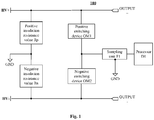
- Fig. 1 is a module structural diagram of an insulation detection device according to an embodiment of the present disclosure.
- the insulation detection device 100 in the embodiment includes a positive switching device OM1, a negative switching device OM2, a sampling unit F1, a reference voltage terminal GND, and a processor D1.
- a positive electrode of an energy storage device is connected to a first end of the positive switching device OM1
- a negative electrode of the energy storage device is connected to a first end of the negative switching device OM2
- a second end of the positive switching device OM1 and a second end of the negative switching device OM2 are respectively connected to a first end of the sampling unit F1
- a second end of the sampling unit F1 is connected to the reference voltage terminal.
- the sampling unit F1 is configured to collect a positive sampled signal on the energy storage device when the positive switching device OM1 and the negative switching device OM2 are in a first switching state, and to collect a negative sampled signal on the energy storage device when the positive switching device OM1 and the negative switching device OM2 are in a second switching state.
- the processor D1 is connected to a third end of the sampling unit F1, and the processor D1 is configured to determine a positive insulation resistance value and a negative insulation resistance value of the energy storage device according to the positive sampled signal and the negative sampled signal.
- the first switching state includes a switch-on state of the positive switching device OM1 and a switch-off state of the negative switching device OM2
- the second switching state includes a switch-off state of the positive switching device OM1 and a switch-on state of the negative switching device OM2.
- the embodiment it is possible to use a same sampling channel to respectively sample a voltage value of the high voltage positive electrode relative to the ground and a voltage value of the high voltage negative electrode relative to the ground, thereby reducing the circuit complexity. Moreover, it is possible to avoid interference and influence on the sampled data due to the difference between different sampling circuits when voltage sampling is performed by a plurality of sampling circuits, thereby improving the measurement accuracy of the sampled signal during insulation detection.
- FIG. 2 shows a module structural diagram of the insulation detection device according to another embodiment of the present disclosure.
- the insulation detection device may further include an insulation detection sampling point S1 (which may be simply referred to as a sampling point S1 hereinafter).
- the sampling point S1 may be positioned at the third end of the sampling unit F1 and connected to the processor D1.
- the positive switching device OM1 and the negative switching device OM2 are configured to allow the positive sampled signal to be collected from the positive electrode of the energy storage device at the insulation detection sampling point S1 when the OM1 and OM2 are in the first switching state, and allow the negative sampled signal to be collected from the negative electrode of the energy storage device at the insulation detection sampling point S1 when the OM1 and OM2 are in the second switching state.
- the first switching state includes the switch-on state of the positive switching device OM1 and the switch-off state of the negative switching device OM2
- the second switching state includes the switch-off state of the positive switching device OM1 and the switch-on state of the negative switching device OM2.
- the sampling unit F1 is connected to the reference voltage terminal.
- the actual voltage at the reference voltage terminal GND can be set according to working environment and requirements of an insulation detection circuit.
- the reference voltage terminal GND may be, for example, a low voltage ground.
- the low pressure ground may be a vehicle body ground, which means that a voltage at a chassis of the vehicle is used as the reference voltage.
- Such grounding can be implemented by contact between metal conductors, and the connection resistance and reactance are generally very small to ensure good grounding.
- the voltage at the reference voltage terminal GND is the reference voltage in the insulation detecting circuit, that is, the reference voltage. For example, if the actual voltage at the reference voltage terminal GND is 6V and the actual voltage of the sampled signal collected at the sampling point S1 is 22V, the voltage of the sampled signal collected at the sampling point S1 can be recorded as 16V.
- the actual voltage of the sampled signal collected at the sampling point S1 is determined by taking the reference voltage terminal GND as the low voltage ground as an example, but the exemplary description should not be construed as a limitation to the reference voltage terminal.
- the positive switching device and the negative switching device are usually positioned at a high voltage side, and the sampling unit is usually positioned at a low voltage side.
- the positive switching device OM1 and the negative switching device OM2 may be isolation switches such as an optical coupler.
- the optical coupler may also be referred to as a photoelectric isolator or a photoelectric coupler, simply referred to as an optocoupler.
- the optical coupler is an electrical-optical-electrical conversion device that transmits an electrical signal in the form of light, and is composed of a light emitting element and a photosensitive element.
- the optical coupler can encapsulate the light emitting element and the photosensitive element in a same closed case, and the light emitting element and the photosensitive element are separated by a transparent insulator.
- the light emitting element can convert an input electrical signal into an optical signal and transmit the optical signal to the photosensitive element with the light as a transmission medium, and the photosensitive element can convert the optical signal to an electrical signal to be output. Since there is no direct electrical connection, while coupling and transmitting signals, the interference on low voltage signals caused by high voltage signals can be effectively controlled and the isolated control of high and low voltage signals can be realized.
- the light emitting element may be, for example, a light emitting diode
- the photosensitive element may be, for example, a photodiode or a phototransistor.
- conversion circuits of different levels can be utilized to control the switch-on and switch-off of the positive switching device and the negative switching device.
- the positive switching device OM1 when a conversion circuit of the positive switching device OM1 outputs a high level, the positive switching device OM1 can be controlled to be in the switch-on state; and when the conversion circuit of the positive switching device OM1 outputs a low level, the positive switching device OM1 can be controlled to be in the switch-off state.
- the negative switching device OM2 when a conversion circuit of the negative switching device OM2 outputs a high level, the negative switching device OM2 can be controlled to be in the switch-on state; and when the conversion circuit of the negative switching device OM2 outputs a low level, the negative switching device OM2 can be controlled to be in the switch-off state.
- the isolated control of high and low voltages is implemented by using the optocoupler, no additional isolation unit for the isolated control is required between a high voltage ground signal and a low voltage ground signal, and thus the circuit structure may be simplified.
- the isolation switches are used and the insulation detection circuit does not need to additionally include an isolation module, which can avoid introducing a new interference signal, thereby improving the accuracy of the sampled signal.
- Fig. 3 is a circuit structural diagram of an insulation detection device according to an exemplary embodiment of the present disclosure.
- Fig. 3 schematically shows specific structures of the positive switching device OM1, the negative switching device OM2, the sampling unit F1, and the reference voltage terminal GND.
- the positive switching device OM1 may include a positive isolation switch, and the positive electrode of the energy storage device is connected to the first end of the sampling unit F1 through the positive isolation switch;
- the negative switching device OM2 may include a negative isolation switch, and the negative electrode of the energy storage device is connected to the first end of the sampling unit F1 through the negative isolation switch.
- the sampling unit F1 may include a sampling isolation switch OM3, a first resistor network R1, and a second resistor network R2.
- a first end of the sampling isolation switch OM3 is connected to the second end of the positive switching device OM1 and the second end of the negative switching device OM2.
- a second end of the sampling isolation switch OM3 is connected to a first end of the first resistor network R1.
- a second end of the first resistor network R1 is connected to a first end of the second resistor network R2; a second end of the second resistor network R2 may be connected to the reference voltage terminal GND.
- the first resistor network R1 and the second resistor network R2 can function as a voltage divider.
- a variation range of the positive sampled signal collected at the sampling point S1 in the first switching state and a variation range of the negative sampled signal collected at the sampling point S1 in the second switching state may be adjusted.
- the combination form and the resistance values of the first resistor network R1 and the second resistor network R2 can be set according to actual conditions in an actual application scenario of battery insulation detection.
- the sampling isolation switch OM3 may also be an isolation switch such as an optocoupler. Conversion circuits of different levels can be utilized to control the switch-on and switch-off of the sampling isolation switch OM3. As an example, the sampling isolation switch OM3 can be controlled to be in the switch-on state when a conversion circuit of the sampling isolation switch OM3 outputs a high level; and the sampling isolation switch OM3 can be controlled to be in the switch-off state when the conversion circuit of the sampling isolation switch OM3 outputs a low level.
- the insulation detection sampling point S1 is connected to the second end of the first resistor network R1, the first end of the second resistor network R2, and the processor D1.
- the sampling isolation switch OM3 is in the switch-on state: in the first switching state of the positive switching device OM1 and the negative switching device OM2, the sampling unit F1 supplies a positive sampled signal to the sampling point S1, and in the second switching state of the positive switching device OM1 and the negative switching device OM2, the sampling unit F1 supplies a negative sampled signal to the sampling point S1.
- the first switching state includes the switch-on state of the positive switching device OM1 and the switch-off state of the negative switching device OM2
- the second switching state includes the switch-off state of the positive switching device OM1 and the switch-on state of the negative switching device OM2.
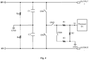
- Fig. 4 is a circuit structural diagram of an insulation detection device according to another exemplary embodiment of the present disclosure.
- the first resistor network R1 and the second resistor network R2 may be regarded as a sampling resistor network of the sampling module F1.
- the insulation detection device of the energy storage system may further include an acceleration switch OM4 and an acceleration resistor network R3.
- An end of the acceleration switch OM4 is connected to the first end of the first resistor network R1, and the other end of the acceleration switch OM4 is connected to an end of the acceleration resistor network R3; and the other end of the acceleration resistor network R3 is connected to the second end of the second resistor network R2.
- the acceleration switch OM4 may be an isolation switch such as an optocoupler. Conversion circuits of different levels can be utilized to control the switch-on and switch-off of the acceleration switch OM4. As an example, the acceleration switch OM4 can be controlled to be in the switch-on state when a conversion circuit of the acceleration switch OM4 outputs a high level; and the acceleration switch OM4 can be controlled to be in the switch-off state when the conversion circuit of the acceleration switch OM4 outputs a low level.
- a distributed capacitor may exist between an energy storage high voltage and an energy storage low voltage, which is an equivalent capacitor between a high voltage component of the energy storage device and a low voltage component of the energy storage device.
- the insulation detection device in embodiments of the present disclosure employs the isolation switches to perform an isolated control of a high voltage end and a low voltage end of the energy storage system.
- a first distributed capacitor exists between the positive electrode of the energy storage device and the reference voltage terminal, and a second distributed capacitor exists between the negative electrode of the energy storage device and the reference voltage terminal.
- the sampling unit F1 needs to collect a stable positive sampled signal provided by the energy storage device, such as a stable voltage value at the positive electrode of the energy storage device relative to the low voltage ground, when the positive switching device OM1 and the negative switching device OM2 are in the first switching state; and collect a stable negative sampled signal provided by the energy storage device, such as a stable voltage value at the negative electrode of the energy storage device relative to the low voltage ground, when the positive switching device OM1 and the negative switching device OM2 are in the second switching state.
- a stable positive sampled signal provided by the energy storage device such as a stable voltage value at the positive electrode of the energy storage device relative to the low voltage ground
- the acceleration switch OM4 when the positive switching device OM1 and the negative switching device OM2 are in the first switching state and a capacitance value of the second distributed capacitor is a determined value, the acceleration switch OM4 is switched on and thus the acceleration resistor network R3 can be connected in the insulation detection device, thereby accelerating the voltage stabilization on the second distributed capacitor and shortening the sampling time for the positive sampled signal; and when the positive switching device OM1 and the negative switching device OM2 are in the second switching state and a capacitance value of the first distributed capacitor is a determined value, the acceleration resistor network R3 can be connected in the insulation detection device, thereby accelerating the voltage stabilization on the first distributed capacitor and shortening the sampling time for the negative sampled signal.
- a resistance value of an equivalent resistor R in an RC charge and discharge circuit can be reduced by paralleling resistors.
- the charging and discharging of the capacitor C can be accelerated and the voltage of the energy storage system can be stabilized more quickly.
- a first insulation detection circuit may be formed by the positive electrode of the energy storage device, the first distributed capacitor C1, the first resistor network R1, the second resistor network R2, the acceleration resistor network R3, and the negative electrode of the energy storage device.
- the first insulation detection circuit can be used to collect the negative sampled signal of the energy storage device.
- the first insulation detection circuit can be simplified as an RC1 charge and discharge circuit in which an equivalent resistor R and the first distributed capacitor C1 are connected in series.
- a power supply for the charge and discharge circuit is in the form of a voltage source.
- an initial voltage on the first distributed capacitor C1 is, for example, V 0
- a stabilized voltage on the first distribution capacitor C1 is V 1
- V t1 represents the voltage value on the first distributed capacitor C1 at any time t1
- RC1 is the product of the resistance value of the equivalent resistor R and the capacitance value of the first distributed capacitor C1. That is, RC1 may represent a time constant, and exp may represent an exponential function with the natural constant e as the base.
- V t2 represents the voltage value on the first distributed capacitor C1 at any time t2
- RC1 is the product of the resistance value of the equivalent resistor R and the capacitance value of the first distributed capacitor C1. That is, RC1 may represent a time constant, and exp may represent an exponential function with the natural constant e as the base.
- the sampling unit F1 includes the first resistor network R1 and the second resistor network R2, the resistance value of the sampling resistor network of the sampling unit F1 is a sum of the resistance value of the first resistor network R1 and the resistance value of the second resistor network R2, and the acceleration resistor network R3 is connected in parallel with the sampling resistor network of the sampling unit F1. Therefore, in the first insulation detection circuit, the resistance value of the equivalent resistor R may be dependent on a total resistance value of the acceleration resistor network R3 in parallel with the first resistor network R1 and the second resistor network R2 of the sampling unit F1.
- the acceleration resistor network R3 can be connected in parallel with the sampling unit F1.
- a second insulation detection circuit may be formed by the positive electrode of the energy storage device, the first resistor network R1, the second resistor network R2, the acceleration resistor network R3, the second distributed capacitor C2, and the negative electrode of the energy storage device.
- the second insulation detection circuit can be used to collect the positive sampled signal of the energy storage device.
- the second insulation detection circuit can be simplified as an RC2 charge and discharge circuit in which the equivalent resistor R and the second distributed capacitor C2 are connected in series.
- the acceleration resistor network R3 when collecting the positive sampled signal of the energy storage device, the acceleration resistor network R3 can be connected in parallel with the sampling resistor network of the sampling unit F1.
- the voltage across the acceleration resistor network R3 should meet a preset voltage requirement, and the power of the acceleration resistor network R3 should meet a preset power requirement.
- the resistance value of the acceleration resistor network R3 can be calculated based on the voltage across the acceleration resistor network R3 and the power of the acceleration resistor network R3.
- the voltage across the acceleration resistor network R3 should be lower than a maximum voltage that the resistor network can withstand under the operating voltage of the energy storage system; and the power of the acceleration resistor network R3 should be less than a rated power of the acceleration resistor network R3.
- the insulation detection device may further include a processor D1 connected to the sampling unit F1.
- the processor D1 is configured to calculate the positive insulation resistance value and the negative insulation resistance value of the energy storage device according to the positive sampled signal and the negative sampled signal collected by the sampling unit F1.
- the insulation detection device further includes an analog to digital converter (ADC).
- ADC analog to digital converter
- the analog to digital converter ADC is connected to the sampling unit F1 and the processor D1, and configured to convert an analog signal acquired by the sampling unit F1 into a digital signal.
- the processor D1 may be connected to the insulation detection sampling point S1 and configured to collect the positive sampled signal of the energy storage device via the sampling point S1 when the positive switching device OM1 and the negative switching device OM2 are in the first switching state and collect the negative sampled signal of the energy storage device via the sampling point S1 when the positive switching device OM1 and the negative switching device OM2 are in the second switching state.
- the processor D1 is configured to calculate a positive insulation resistance value and a negative insulation resistance value of a power battery pack to be tested according to the positive sampled signal and the negative sampled signal.
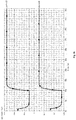
- Fig. 5a shows the relationship between time and the voltage of the insulation detection circuit when the acceleration resistor network is not connected in the insulation detection circuit
- Fig. 5b shows the relationship between time and the voltage of the insulation detection circuit when the acceleration resistor network is connected in the insulation detection circuit.
- curve 1 may be used to depict the relationship between time and the voltage at the high voltage positive electrode of the insulation detection circuit relative to the low voltage ground, when the sampling resistor network of the sampling unit is not connected in parallel with the acceleration resistor network;
- curve 2 may be used to depict the relationship between time and the voltage at the high voltage negative electrode of the insulation detection circuit relative to the low voltage ground, when the sampling resistor network of the sampling unit is not connected in parallel with the acceleration resistor network.
- the time for voltage stabilization of the insulation detection circuit is about 6.715 seconds.
- curve 3 may be used to depict the relationship between time and the voltage at the high voltage positive electrode of the insulation detection circuit relative to the low voltage ground, when the sampling resistor network of the sampling unit is connected in parallel with the acceleration resistor network;
- curve 4 may be used to depict the relationship between time and the voltage at the high voltage negative electrode of the insulation detection circuit relative to the low voltage ground, when the sampling resistor network of the sampling unit is connected in parallel with the acceleration resistor network.
- the time for voltage stabilization of the insulation detection circuit is about 3.631 seconds, which is shorter than the time for voltage stabilization when the resistor network of the sampling unit is not connected in parallel with the acceleration resistor network. Therefore, the insulation sampling speed is faster, the insulation sampling efficiency is higher, and the insulation sampling when the voltage is not stable may be avoided so as not to affect the sampling accuracy. In other words, the insulation sampling accuracy may be improved, the sampling time may be shortened, and the sampling efficiency may be improved.
- the charging and discharging time of the equivalent capacitor may be reduced by way of paralleling the sampling circuit of the sampling unit with the acceleration resistor, so that the insulation detection circuit may reach a stable voltage state as fast as possible.
- the sampling time may be shortened, and the sampling efficiency and the sensitivity of the insulation resistance may be improved.
- Fig. 6 is a circuit diagram of the insulation detection device for collecting sampled signals from the energy storage device according to an exemplary embodiment of the present disclosure
- Fig. 7 is a simplified circuit structural diagram of the insulation detection device when collecting the positive sampled signal of the energy storage device according to an embodiment of the present disclosure
- Fig. 8 is a simplified circuit structural diagram of the insulation detection device when collecting the negative sampled signal of the energy storage device according to an embodiment of the present disclosure.
- the first positive sampled signal can be converted into the first positive sampled voltage and the first negative sampled signal can be converted into the first negative sampled voltage. According to the first positive sampled voltage and the first negative sampled voltage, the positive insulation resistance value and the negative insulation resistance value of the energy storage device can be determined.
- the processor D1 can collect the first positive sampled signal at the sampling point S1, and determine the first positive sampled voltage U c1 at the high voltage positive electrode of the energy storage device relative to the low voltage ground when the positive switching device and the negative switching device are in the first switching state.
- an input voltage (HV voltage) between the high voltage positive electrode and the high voltage negative electrode in the energy storage system is denoted by U bat .
- U c1 is the first positive sampled voltage at the high voltage positive electrode relative to the low voltage ground, which corresponds to the first positive sampled signal in the energy storage device;
- R1 is the resistance value of the first resistor network;
- R2 is the resistance value of the second resistor network;
- Rp is the positive insulation resistance value;
- Rn is the negative insulation resistance value;
- U bat is the input voltage between the high voltage positive electrode and the high voltage negative electrode.
- the processor D1 can collect the first negative sampled signal at the sampling point S1, and determine the first negative sampled voltage U a1 at the high voltage negative electrode of the energy storage device relative to the low voltage ground when the positive switching device and the negative switching device are in the second switching state. That is, the voltage at the high voltage negative electrode relative to the low voltage ground in the energy storage system is the first negative sampled voltage U a1 .
- an input voltage (HV) between the high voltage positive electrode and the high voltage negative electrode in the energy storage system is denoted by U bat .
- U bat is the input voltage between the high voltage positive electrode and the high voltage negative electrode
- U a1 is the first negative sampled voltage at the high voltage negative electrode relative to the low voltage ground, which corresponds to the first negative sampled signal in the energy storage system
- Rp is the positive insulation resistance value
- Rn is the negative insulation resistance value
- R1 is the resistance value of the first resistor network
- R2 is the resistance value of the second resistor network.
- the equations of the expression (5) and the expression (6) are combined and solved to obtain the positive insulation resistance value Rp of the energy storage device and the negative insulation resistance value Rn of the energy storage device as shown in the following expression (7).
- ⁇ Rp U bat ⁇ U c 1 ⁇ U a 1 ⁇ R 1 + R 2 / U a 1
- Rn U bat ⁇ U c 1 ⁇ U a 1 ⁇ R 1 ⁇ R 2 / U c 1
- Rp is the positive insulation resistance value
- Rn is the negative insulation resistance value
- U bat is the input voltage between the high voltage positive electrode and the high voltage negative electrode
- U c1 is the first positive sampled voltage at the high voltage positive electrode relative to the low voltage ground, which corresponds to the first positive sampled signal in the energy storage device
- U a1 is the first negative sampled voltage at the high voltage negative electrode relative to the low voltage ground, which corresponds to the first negative sampled signal in the energy storage system
- R1 is the resistance value of the first resistor network
- R2 is the resistance value of the second resistor network.
- control the acceleration switch to switch on control the positive switching device to switch on and control the negative switching device to switch off, and collect the second positive sampled signal by the insulation detection device
- control the acceleration switch to switch on control the positive switching device to switch off and control the negative switching device to switch on, and collect the second negative sampled signal by the insulation detection device
- the insulation detection method may further include converting the second positive sampled signal into the second positive sampled voltage; converting the second negative sampled signal into the second negative sampled voltage; and calculate the positive insulation resistance value and the negative insulation resistance value of the energy storage device according to the second positive sampled voltage and the second negative sampled voltage.
- the positive switching device OM1 and the negative switching device OM2 are in the first switching state, and the acceleration resistor network R3 is in parallel with the first resistor network and the second resistor network of the sampling unit F1.
- the processor D1 can collect the second positive sampled signal at the sampling point S1, and determine the second positive sampled voltage U c2 at the high voltage positive electrode of the energy storage device relative to the low voltage ground when the positive switching device and the negative switching device are in the first switching state. That is, the voltage at the high voltage positive electrode relative to the low voltage ground in the energy storage system is the second positive sampled voltage U c2 .
- an input voltage (HV voltage) between the high voltage positive electrode and the high voltage negative electrode in the energy storage system is denoted by U bat .
- U c2 is the second positive sampled voltage at the high voltage positive electrode relative to the low voltage ground, which corresponds to the second positive sampled signal in the energy storage device;
- R1 is the resistance value of the first resistor network;
- R2 is the resistance value of the second resistor network;
- R3 is the resistance value of the acceleration resistor network;
- Rp is the positive insulation resistance value;
- Rn is the negative insulation resistance value;
- U bat is the input voltage between the high voltage positive electrode and the high voltage negative electrode.
- the positive switching device OM1 and the negative switching device OM2 are in the second switching state, and the acceleration resistor network R3 is in parallel with the first resistor network and the second resistor network of the sampling unit F1.
- the processor D1 can collect the second negative sampled signal at the sampling point S1, and determine the second negative sampled voltage U a2 at the high voltage negative electrode of the energy storage device relative to the low voltage ground when the positive switching device and the negative switching device are in the second switching state. That is, the voltage at the high voltage negative electrode relative to the low voltage ground in the energy storage system is the second negative sampled voltage U a2 .
- an input voltage (HV voltage) between the high voltage positive electrode and the high voltage negative electrode in the energy storage system is denoted by U bat .
- U bat is the input voltage between the high voltage positive electrode and the high voltage negative electrode
- U a2 is the second negative sampled voltage at the high voltage negative electrode relative to the low voltage ground, which corresponds to the second negative sampled signal in the energy storage system
- Rp is the positive insulation resistance value
- Rn is the negative insulation resistance value
- R1 is the resistance value of the first resistor network
- R2 is the resistance value of the second resistor network
- R3 is the resistance value of the acceleration resistor network.
- the equations of the expression (8) and the expression (9) are combined and solved to obtain the positive insulation resistance value Rp of the energy storage device and the negative insulation resistance value Rn of the energy storage device as shown in the following expression (10).
- ⁇ Rp U bat ⁇ U c 2 ⁇ U a 2 ⁇ R 1 + R 2 ⁇ R 3 / R 1 + R 2 + R 3 / U a 2
- Rn U bat ⁇ U c 2 ⁇ U a 2 ⁇ R 1 + R 2 ⁇ R 3 / R 1 + R 2 + R 3 / U c 2
- Rp is the positive insulation resistance value
- Rn is the negative insulation resistance value
- U bat is the input voltage between the high voltage positive electrode and the high voltage negative electrode
- U c2 is the second positive sampled voltage at the high voltage positive electrode relative to the low voltage ground, which corresponds to the second positive sampled signal in the energy storage device
- U a2 is the second negative sampled voltage at the high voltage negative electrode relative to the low voltage ground, which corresponds to the second negative sampled signal in the energy storage system
- R1 is the resistance value of the first resistor network
- R2 is the resistance value of the second resistor network
- R3 is the resistance value of the acceleration resistor network.
- the insulation detection method may further include determine a lower resistance value of the positive insulation resistance value and the negative insulation resistance value as an insulation resistance value of the energy storage system; compare the insulation resistance value of the energy storage system and a preset insulation resistance threshold to obtain a comparison result of the insulation resistance value of the energy storage system; and determine an insulation state of the energy storage system according to the comparison result of the insulation resistance value of the energy storage system.
- the insulation resistance value of the energy storage system is higher than the preset insulation resistance threshold, it may be determined that the insulation state of the energy storage system is an alarm state and an alarm message may be input according to the alarm state of the energy storage system.
- the insulation detection can be implemented by a single sampling module, thereby avoiding the influence of a multichannel AD sampling difference on the insulation detection. Further, when the acceleration resistor is connected in parallel on the sampling unit, a fast insulation sampling can be realized, and the sensitivity of the insulation resistance can be improved.
- the processor D1 in the embodiments of the present disclosure may be a processing device dedicated to the insulation detection circuit, or may be a processing device to be shared with other circuits.
- the insulation detection circuit can be an independent circuit structure or a part of an overall circuit structure.
- the insulation detection device in the embodiments of the present disclosure may be integrated in a battery management system of an energy storage device such as a power battery pack of a new energy vehicle.
- a part of an overall circuit structure of the battery management system may be used for insulation detection on the energy storage device, and a central processing unit of the battery management system may calculate the positive insulation resistance value and the negative insulation resistance value of the energy storage device.
- the above embodiments may be implemented entirely or partly by software, hardware, firmware or any combination thereof.
- software it may be entirely or partly implemented as a computer program product or a computer readable storage medium.
- the computer program product or the computer readable storage medium includes one or more computer instructions.
- the computer program instructions When the computer program instructions are loaded and executed on a computer, they entirely and partly produce the flowchart or functions described in the embodiments of the present disclosure.
- the computer may be a general purpose computer, a special purpose computer, a computer network, or another programmable apparatus.
- the computer instructions may be stored in the computer readable storage medium or may be transmitted from a computer readable storage medium to another computer readable storage medium.
- the computer instructions may be transmitted by wire (for example, coaxial cable, optical fiber, digital subscriber line (DSL)) or wireless (for example, infrared, radio, microwave and so on) from a website, computer, server or data center to another website, computer, server or data center.
- the computer readable storage medium may be any applicable medium accessible by the computer or a data storage device such as a server or a data center integrated with one or more applicable media.
- the applicable medium may be a magnetic medium (for example, a soft disk, a hard disk, a magnetic tape), an optical medium (for example, a DVD) or a semiconductor medium (for example, a solid state disk (SSD)) and so on.
Landscapes
- Physics & Mathematics (AREA)
- General Physics & Mathematics (AREA)
- Engineering & Computer Science (AREA)
- Chemical & Material Sciences (AREA)
- Combustion & Propulsion (AREA)
- Life Sciences & Earth Sciences (AREA)
- Sustainable Development (AREA)
- Sustainable Energy (AREA)
- Power Engineering (AREA)
- Transportation (AREA)
- Mechanical Engineering (AREA)
- Measurement Of Current Or Voltage (AREA)
Abstract
Description
- The present disclosure relates to the field of energy storage systems, and particularly to an insulation detection device and method for an energy storage system.
- The energy storage system is used to store and supply electrical energy. In the energy storage system, an insulation fault may directly affect normal operations of equipment, and even cause a safety accident in severe cases. For example, when a short circuit is formed between a high voltage positive electrode and the ground and a person touches a corresponding high voltage negative electrode, loss of life and property may be caused.
- Therefore, it is necessary to conduct insulation detection on the energy storage system to monitor in real-time whether an insulation resistance value between the positive and negative electrodes of the energy storage system reaches a standard value, thereby avoiding safety issues caused by the insulation resistance value between the positive and negative electrodes of the energy storage system failing to reach the standard value.
- At present, when conducting insulation sampling on an energy storage device in the energy storage system, it is generally required to collect data about the positive insulation resistance and the negative insulation resistance of the energy storage device on different sampling channels, and derive the positive insulation resistance and the negative insulation resistance according to the data collected on the different sampling channels. An insulation sampling circuit may have a high complexity and measurement accuracy of the insulation resistance may be limited.
- The embodiments of the present disclosure provide an insulation detection device and method for an energy storage system, so as to reduce the circuit complexity, improve the measurement accuracy of the insulation detection and the sensitivity of the insulation resistance and also reduce the time for insulation detection.
- In a first aspect, the embodiments of the present disclosure provide an insulation detection device for an energy storage system. The insulation detection device includes a positive switching device, a negative switching device, a sampling unit, a reference voltage terminal and a processor.
- A positive electrode of an energy storage device is connected to a first end of the positive switching device, a negative electrode of the energy storage device is connected to a first end of the negative switching device, a second end of the positive switching device and a second end of the negative switching device are respectively connected to a first end of the sampling unit, and a second end of the sampling unit is connected to the reference voltage terminal.
- The sampling unit is configured to collect a positive sampled signal on the energy storage device when the positive switching device and the negative switching device are in a first switching state, and to collect a negative sampled signal on the energy storage device when the positive switching device and the negative switching device are in a second switching state.
- The processor is connected to a third end of the sampling unit, and configured to determine a positive insulation resistance value and a negative insulation resistance value of the energy storage device according to the positive sampled signal and the negative sampled signal.
- In some embodiments according to the first aspect, the sampling unit includes a sampling isolation switch, a first resistor network and a second resistor network, wherein a first end of the sampling isolation switch is connected to the second end of the positive switching device and the second end of the negative switching device; a second end of the sampling isolation switch is connected to a first end of the first resistor network; a second end of the first resistor network is connected to a first end of the second resistor network; and a second end of the second resistor network is connected to the reference voltage terminal.
- In some embodiments according to the first aspect, the insulation detection device further includes an acceleration switch and an acceleration resistor network, wherein a first end of the acceleration switch is connected to the first end of the first resistor network, and a second end of the acceleration switch is connected to a first end of the acceleration resistor network; and a second end of the acceleration resistor network is connected to the second end of the second resistor network.
- In some embodiments according to the first aspect, the insulation detection device further includes an insulation detection sampling point positioned at the third end of the sampling unit and connected to the processor.
- The sampling unit is further configured to collect the positive sampled signal on the energy storage device via the insulation detection sampling point when the positive switching device and the negative switching device are in the first switching state; and collect the negative sampled signal on the energy storage device via the insulation detection sampling point when the positive switching device and the negative switching device are in the second switching state.
- In some embodiments according to the first aspect, the insulation detection device further includes an insulation detection sampling point connected to the second end of the first resistor network, the first end of the second resistor network and the processor.
- In some embodiments according to the first aspect, the first switching state includes a switch-on state of the positive switching device and a switch-off state of the negative switching device; and the second switching state includes a switch-off state of the positive switching device and a switch-on state of the negative switching device.
- In some embodiments according to the first aspect, the positive switching device includes a positive isolation switch, and the positive electrode of the energy storage device is connected to the first end of the sampling unit through the positive isolation switch; and the negative switching device includes a negative isolation switch, and the negative electrode of the energy storage device is connected to the first end of the sampling unit through the negative isolation switch.
- In some embodiments according to the first aspect, the processor is further configured to determine a lower resistance value of the positive insulation resistance value and the negative insulation resistance value as an insulation resistance value of the energy storage system; compare the insulation resistance value of the energy storage system and a preset insulation resistance threshold to obtain a comparison result of the insulation resistance value of the energy storage system; and determine an insulation state of the energy storage system according to the comparison result of the insulation resistance value of the energy storage system.
- In a second aspect, the embodiments of the present disclosure provide an insulation detection method for an energy storage system to be implemented in the above insulation detection device for the energy storage system. The insulation detection method includes controlling the positive switching device to switch on and the negative switching device to switch off, and collecting a first positive sampled signal by the insulation detection device; controlling the positive switching device to switch off and the negative switching device to switch on, and collecting a first negative sampled signal by the insulation detection device; and calculating the positive insulation resistance value and the negative insulation resistance value of the energy storage device according to the first positive sampled signal and the first negative sampled signal.
- In some embodiments according to the second aspect, calculating the positive insulation resistance value and the negative insulation resistance value of the energy storage device according to the first positive sampled signal and the first negative sampled signal includes: converting the first positive sampled signal into a first positive sampled voltage; converting the first negative sampled signal into a first negative sampled voltage; and calculating the positive insulation resistance value and the negative insulation resistance value of the energy storage device according to the first positive sampled voltage and the first negative sampled voltage.
- In some embodiments according to the second aspect, the insulation detection device further includes an acceleration switch and an acceleration resistor network, and the insulation detection method further includes controlling the acceleration switch to switch on, the positive switching device to switch on and the negative switching device to switch off, and collecting a second positive sampled signal by the insulation detection device; controlling the acceleration switch to switch on, the positive switching device to switch off and the negative switching device to switch on, and collecting a second negative sampled signal by the insulation detection device; and calculating the positive insulation resistance value and the negative insulation resistance value of the energy storage device according to the second positive sampled signal and the second negative sampled signal.
- In some embodiments according to the second aspect, the insulation detection method further includes converting the second positive sampled signal into a second positive sampled voltage; converting the second negative sampled signal into a second negative sampled voltage; and calculating the positive insulation resistance value and the negative insulation resistance value of the energy storage device according to the second positive sampled voltage and the second negative sampled voltage.
- With the insulation detection device and method for the energy storage system according to the embodiments of the present disclosure, it is possible to use a same sampling channel to respectively sample a positive voltage value of the high voltage positive electrode of the energy storage system relative to a reference voltage terminal and a negative voltage value of the high voltage negative electrode of the energy storage system relative to the reference voltage terminal, thereby reducing the circuit complexity, avoiding interference and influence on the insulation detection sampling due to the difference between different sampling channels, and improving the measurement accuracy of the insulation detection.
- Additionally, by paralleling the acceleration resistor network across the resistor network of the sampling unit, the insulation detection circuit may reach a stable voltage state as soon as possible. Thus the sampling time may be shortened, and the sampling efficiency may be improved.
- To more clearly illustrate technical solutions of embodiments of the present disclosure, the accompanying drawings, which are to be referred by the embodiments of the present disclosure, will be briefly described. Those skilled in the art will be able to obtain additional drawings in accordance with these drawings without any creative work.
-
Fig. 1 is a module structural diagram of an insulation detection device according to an embodiment of the present disclosure; -
Fig. 2 is a module structural diagram of an insulation detection device according to another embodiment of the present disclosure; -
Fig. 3 is a circuit structural diagram of an insulation detection device according to an exemplary embodiment of the present disclosure; -
Fig. 4 is a circuit structural diagram of an insulation detection device according to another exemplary embodiment of the present disclosure; -
Fig. 5a illustrates a relationship between time and a voltage of an insulation detection circuit when there is no acceleration resistor network connected in the insulation detection circuit; -
Fig. 5b illustrates a relationship between time and a voltage of an insulation detection circuit when an acceleration resistor network is connected in the insulation detection circuit; -
Fig. 6 is a circuit diagram of an insulation detection device sampling an energy storage device according to an exemplary embodiment of the present disclosure; -
Fig. 7 is a simplified circuit structural diagram of an insulation detection device when collecting a positive sampled signal on an energy storage device according to an embodiment of the present disclosure; and -
Fig. 8 is a simplified circuit structural diagram of an insulation detection device when collecting a negative sampled signal on an energy storage device according to an embodiment of the present disclosure. - Various aspects of features and exemplary embodiments of the present disclosure will be described in detail below. The present disclosure will be provided in further detail below in conjunction with accompanying drawings and embodiments in order to make objects, technical solutions and advantages of the present disclosure to be more clearly understood. It is to be appreciated that the specific embodiments described herein are to be construed to illustrate the present disclosure but not to limit the present disclosure. It will be apparent to those skilled in the art that the present disclosure may be practiced without some of these specific details. The following description of the embodiments is merely to provide a better understanding of the present disclosure by illustrating examples thereof.
- It is to be noted that relational terms such as first, second and the like are used herein only to distinguish an entity or operation from another entity or operation without requiring or implying that there is any such actual relationship or order between these entities or operations. Moreover, the term "comprise", "include" or any other variant thereof is intended to encompass a non-exclusive inclusion, such that a process, method, article or device that includes a series of elements includes not only these elements but also other elements that are not explicitly listed or those elements that are inherent to such a process, method, article or device. In the absence of more restrictions, elements defined by the statement "includes ..." do not preclude the presence of additional identical elements in the process, method, article or device that includes the elements.
- In embodiments of the present disclosure, the energy storage device in the energy storage system may be a variety of types of power storage units. For example, the energy storage device may be a lithium-ion power storage unit, a lead-acid power storage unit, a nickel-cadmium power storage unit, a nickel-hydrogen power storage unit, a lithium-sulfur power storage unit, or a sodium-ion power storage unit. In terms of scale, the power storage unit can be a single cell or a battery module or a battery pack, which is not limited herein.
- An energy storage system generally has a high voltage, such as hundreds of volts. When the energy storage system is in normal operation, positive and negative buses of a battery system and a case of equipment may have good insulation performance. However, if the insulation is damaged during use, leakage of electricity may occur, which may threaten personal and property safety of an operator. Therefore, in a high voltage energy storage system, it is important to detect an insulation resistance of an energy storage device in the energy storage system.
- In view of this, embodiments of the present disclosure provide an insulation detection device and an insulation detection method for the energy storage system. The insulation detect device can monitor in real-time whether an insulation resistance value between positive and negative electrodes of the energy storage device reaches a standard value.
- In order to better understand the present disclosure, the insulation detection device and the insulation detection method for the energy storage system according to embodiments of the present disclosure will be described in detail below with reference to the accompanying drawings. It should be noted that these embodiments are not intended to limit the scope of the present disclosure.
-
Fig. 1 is a module structural diagram of an insulation detection device according to an embodiment of the present disclosure. As shown inFig. 1 , theinsulation detection device 100 in the embodiment includes a positive switching device OM1, a negative switching device OM2, a sampling unit F1, a reference voltage terminal GND, and a processor D1. - In the embodiment, a positive electrode of an energy storage device is connected to a first end of the positive switching device OM1, a negative electrode of the energy storage device is connected to a first end of the negative switching device OM2, a second end of the positive switching device OM1 and a second end of the negative switching device OM2 are respectively connected to a first end of the sampling unit F1, and a second end of the sampling unit F1 is connected to the reference voltage terminal.
- The sampling unit F1 is configured to collect a positive sampled signal on the energy storage device when the positive switching device OM1 and the negative switching device OM2 are in a first switching state, and to collect a negative sampled signal on the energy storage device when the positive switching device OM1 and the negative switching device OM2 are in a second switching state.
- As shown in
Fig. 1 , the processor D1 is connected to a third end of the sampling unit F1, and the processor D1 is configured to determine a positive insulation resistance value and a negative insulation resistance value of the energy storage device according to the positive sampled signal and the negative sampled signal. - In an embodiment, the first switching state includes a switch-on state of the positive switching device OM1 and a switch-off state of the negative switching device OM2, and the second switching state includes a switch-off state of the positive switching device OM1 and a switch-on state of the negative switching device OM2.
- In the embodiment, it is possible to use a same sampling channel to respectively sample a voltage value of the high voltage positive electrode relative to the ground and a voltage value of the high voltage negative electrode relative to the ground, thereby reducing the circuit complexity. Moreover, it is possible to avoid interference and influence on the sampled data due to the difference between different sampling circuits when voltage sampling is performed by a plurality of sampling circuits, thereby improving the measurement accuracy of the sampled signal during insulation detection.
- An insulation detection device for the energy storage system according to another embodiment of the present disclosure may be described below with reference to
Fig. 2 which shows a module structural diagram of the insulation detection device according to another embodiment of the present disclosure. - As shown in
Fig. 2 , in some embodiments, the insulation detection device may further include an insulation detection sampling point S1 (which may be simply referred to as a sampling point S1 hereinafter). The sampling point S1 may be positioned at the third end of the sampling unit F1 and connected to the processor D1. - As shown in
Fig. 2 , the positive switching device OM1 and the negative switching device OM2 are configured to allow the positive sampled signal to be collected from the positive electrode of the energy storage device at the insulation detection sampling point S1 when the OM1 and OM2 are in the first switching state, and allow the negative sampled signal to be collected from the negative electrode of the energy storage device at the insulation detection sampling point S1 when the OM1 and OM2 are in the second switching state. - In the embodiment, the first switching state includes the switch-on state of the positive switching device OM1 and the switch-off state of the negative switching device OM2, and the second switching state includes the switch-off state of the positive switching device OM1 and the switch-on state of the negative switching device OM2.
- With continued reference to
Fig. 2 , in the embodiment of the present disclosure, the sampling unit F1 is connected to the reference voltage terminal. The actual voltage at the reference voltage terminal GND can be set according to working environment and requirements of an insulation detection circuit. - In an embodiment, the reference voltage terminal GND may be, for example, a low voltage ground. As an example, if the insulation detection device is applied to a new energy vehicle, the low pressure ground may be a vehicle body ground, which means that a voltage at a chassis of the vehicle is used as the reference voltage. Such grounding can be implemented by contact between metal conductors, and the connection resistance and reactance are generally very small to ensure good grounding.
- The voltage at the reference voltage terminal GND is the reference voltage in the insulation detecting circuit, that is, the reference voltage. For example, if the actual voltage at the reference voltage terminal GND is 6V and the actual voltage of the sampled signal collected at the sampling point S1 is 22V, the voltage of the sampled signal collected at the sampling point S1 can be recorded as 16V.
- In the following description of the embodiments, the actual voltage of the sampled signal collected at the sampling point S1 is determined by taking the reference voltage terminal GND as the low voltage ground as an example, but the exemplary description should not be construed as a limitation to the reference voltage terminal.
- In the embodiments of the present disclosure, the positive switching device and the negative switching device are usually positioned at a high voltage side, and the sampling unit is usually positioned at a low voltage side. In order to perform an isolated control of high and low voltages, the positive switching device OM1 and the negative switching device OM2 may be isolation switches such as an optical coupler. The optical coupler may also be referred to as a photoelectric isolator or a photoelectric coupler, simply referred to as an optocoupler.
- In an embodiment, the optical coupler is an electrical-optical-electrical conversion device that transmits an electrical signal in the form of light, and is composed of a light emitting element and a photosensitive element. The optical coupler can encapsulate the light emitting element and the photosensitive element in a same closed case, and the light emitting element and the photosensitive element are separated by a transparent insulator.
- For ease of understanding, operation principles of the optical coupler will be briefly described below. In the optical coupler, the light emitting element can convert an input electrical signal into an optical signal and transmit the optical signal to the photosensitive element with the light as a transmission medium, and the photosensitive element can convert the optical signal to an electrical signal to be output. Since there is no direct electrical connection, while coupling and transmitting signals, the interference on low voltage signals caused by high voltage signals can be effectively controlled and the isolated control of high and low voltage signals can be realized.
- In an embodiment, the light emitting element may be, for example, a light emitting diode, and the photosensitive element may be, for example, a photodiode or a phototransistor.
- In the embodiment of the present disclosure, conversion circuits of different levels can be utilized to control the switch-on and switch-off of the positive switching device and the negative switching device.
- As an example, when a conversion circuit of the positive switching device OM1 outputs a high level, the positive switching device OM1 can be controlled to be in the switch-on state; and when the conversion circuit of the positive switching device OM1 outputs a low level, the positive switching device OM1 can be controlled to be in the switch-off state.
- As an example, when a conversion circuit of the negative switching device OM2 outputs a high level, the negative switching device OM2 can be controlled to be in the switch-on state; and when the conversion circuit of the negative switching device OM2 outputs a low level, the negative switching device OM2 can be controlled to be in the switch-off state.
- In an embodiment, if the isolated control of high and low voltages is implemented by using the optocoupler, no additional isolation unit for the isolated control is required between a high voltage ground signal and a low voltage ground signal, and thus the circuit structure may be simplified.
- In the embodiment of the present disclosure, the isolation switches are used and the insulation detection circuit does not need to additionally include an isolation module, which can avoid introducing a new interference signal, thereby improving the accuracy of the sampled signal.
-
Fig. 3 is a circuit structural diagram of an insulation detection device according to an exemplary embodiment of the present disclosure.Fig. 3 schematically shows specific structures of the positive switching device OM1, the negative switching device OM2, the sampling unit F1, and the reference voltage terminal GND. - As shown in
Fig. 3 , in an embodiment, the positive switching device OM1 may include a positive isolation switch, and the positive electrode of the energy storage device is connected to the first end of the sampling unit F1 through the positive isolation switch; the negative switching device OM2 may include a negative isolation switch, and the negative electrode of the energy storage device is connected to the first end of the sampling unit F1 through the negative isolation switch. - In an embodiment, the sampling unit F1 may include a sampling isolation switch OM3, a first resistor network R1, and a second resistor network R2.
- A first end of the sampling isolation switch OM3 is connected to the second end of the positive switching device OM1 and the second end of the negative switching device OM2.
- A second end of the sampling isolation switch OM3 is connected to a first end of the first resistor network R1.
- A second end of the first resistor network R1 is connected to a first end of the second resistor network R2; a second end of the second resistor network R2 may be connected to the reference voltage terminal GND.
- In the embodiment, the first resistor network R1 and the second resistor network R2 can function as a voltage divider. By adjusting the resistance value of the first resistor network R1 and the resistance value of the second resistor network R2, a variation range of the positive sampled signal collected at the sampling point S1 in the first switching state and a variation range of the negative sampled signal collected at the sampling point S1 in the second switching state may be adjusted.
- It should be noted that the combination form and the resistance values of the first resistor network R1 and the second resistor network R2 can be set according to actual conditions in an actual application scenario of battery insulation detection.
- In an embodiment, the sampling isolation switch OM3 may also be an isolation switch such as an optocoupler. Conversion circuits of different levels can be utilized to control the switch-on and switch-off of the sampling isolation switch OM3. As an example, the sampling isolation switch OM3 can be controlled to be in the switch-on state when a conversion circuit of the sampling isolation switch OM3 outputs a high level; and the sampling isolation switch OM3 can be controlled to be in the switch-off state when the conversion circuit of the sampling isolation switch OM3 outputs a low level.
- With continued reference to
Fig. 3 , in an embodiment, in the insulation detection device, the insulation detection sampling point S1 is connected to the second end of the first resistor network R1, the first end of the second resistor network R2, and the processor D1. When the sampling isolation switch OM3 is in the switch-on state: in the first switching state of the positive switching device OM1 and the negative switching device OM2, the sampling unit F1 supplies a positive sampled signal to the sampling point S1, and in the second switching state of the positive switching device OM1 and the negative switching device OM2, the sampling unit F1 supplies a negative sampled signal to the sampling point S1. - As described in the foregoing embodiments, the first switching state includes the switch-on state of the positive switching device OM1 and the switch-off state of the negative switching device OM2, and the second switching state includes the switch-off state of the positive switching device OM1 and the switch-on state of the negative switching device OM2.
- An insulation detection device for the energy storage system according to another embodiment of the present disclosure will be described in detail below with reference to
Fig. 4 ,Fig. 5a andFig. 5b .Fig. 4 is a circuit structural diagram of an insulation detection device according to another exemplary embodiment of the present disclosure. - For convenience of description, in the following embodiments, the first resistor network R1 and the second resistor network R2 may be regarded as a sampling resistor network of the sampling module F1.
- As shown in
Fig. 4 , in an embodiment, the insulation detection device of the energy storage system may further include an acceleration switch OM4 and an acceleration resistor network R3. - An end of the acceleration switch OM4 is connected to the first end of the first resistor network R1, and the other end of the acceleration switch OM4 is connected to an end of the acceleration resistor network R3; and the other end of the acceleration resistor network R3 is connected to the second end of the second resistor network R2.
- In an embodiment, the acceleration switch OM4 may be an isolation switch such as an optocoupler. Conversion circuits of different levels can be utilized to control the switch-on and switch-off of the acceleration switch OM4. As an example, the acceleration switch OM4 can be controlled to be in the switch-on state when a conversion circuit of the acceleration switch OM4 outputs a high level; and the acceleration switch OM4 can be controlled to be in the switch-off state when the conversion circuit of the acceleration switch OM4 outputs a low level.
- In embodiments of the present disclosure, a distributed capacitor may exist between an energy storage high voltage and an energy storage low voltage, which is an equivalent capacitor between a high voltage component of the energy storage device and a low voltage component of the energy storage device. The insulation detection device in embodiments of the present disclosure employs the isolation switches to perform an isolated control of a high voltage end and a low voltage end of the energy storage system. A first distributed capacitor exists between the positive electrode of the energy storage device and the reference voltage terminal, and a second distributed capacitor exists between the negative electrode of the energy storage device and the reference voltage terminal.
- In embodiments of the present disclosure, the sampling unit F1 needs to collect a stable positive sampled signal provided by the energy storage device, such as a stable voltage value at the positive electrode of the energy storage device relative to the low voltage ground, when the positive switching device OM1 and the negative switching device OM2 are in the first switching state; and collect a stable negative sampled signal provided by the energy storage device, such as a stable voltage value at the negative electrode of the energy storage device relative to the low voltage ground, when the positive switching device OM1 and the negative switching device OM2 are in the second switching state.
- In the embodiment, when the positive switching device OM1 and the negative switching device OM2 are in the first switching state and a capacitance value of the second distributed capacitor is a determined value, the acceleration switch OM4 is switched on and thus the acceleration resistor network R3 can be connected in the insulation detection device, thereby accelerating the voltage stabilization on the second distributed capacitor and shortening the sampling time for the positive sampled signal; and when the positive switching device OM1 and the negative switching device OM2 are in the second switching state and a capacitance value of the first distributed capacitor is a determined value, the acceleration resistor network R3 can be connected in the insulation detection device, thereby accelerating the voltage stabilization on the first distributed capacitor and shortening the sampling time for the negative sampled signal.
- In the embodiments of the present disclosure, according to the principle of RC charging and discharging, a resistance value of an equivalent resistor R in an RC charge and discharge circuit can be reduced by paralleling resistors. In the RC charge and discharge circuit, when a capacitance value of a capacitor C is determined, by reducing the resistance value of the resistor R, the charging and discharging of the capacitor C can be accelerated and the voltage of the energy storage system can be stabilized more quickly.
- For ease of understanding, the operation principle of accelerating voltage stabilization by using the acceleration resistor network R3 so as to shorten the insulation sampling time, will be described below by way of a specific embodiment.
- As shown in
Fig. 4 , in an embodiment, when the sampling isolation switch OM3 and the acceleration switch OM4 are in the switch-on state and the positive switching device OM1 and the negative switching device OM2 are in the second switching state, a first insulation detection circuit may be formed by the positive electrode of the energy storage device, the first distributed capacitor C1, the first resistor network R1, the second resistor network R2, the acceleration resistor network R3, and the negative electrode of the energy storage device. The first insulation detection circuit can be used to collect the negative sampled signal of the energy storage device. The first insulation detection circuit can be simplified as an RC1 charge and discharge circuit in which an equivalent resistor R and the first distributed capacitor C1 are connected in series. - In an embodiment, a power supply for the charge and discharge circuit is in the form of a voltage source. Assuming that the first distributed capacitor C1 is charged through the equivalent resistor R, an initial voltage on the first distributed capacitor C1 is, for example, V0, and a stabilized voltage on the first distribution capacitor C1 is V1, then a charging voltage on the first distributed capacitor C1 at any time t1 can be expressed as the following expression (1):

- The charging time T1 of the first distributed capacitor C1 can be determined by the above expression (1) and expressed as the following expression (2):

- In the above expressions (1) and (2), Vt1 represents the voltage value on the first distributed capacitor C1 at any time t1, and RC1 is the product of the resistance value of the equivalent resistor R and the capacitance value of the first distributed capacitor C1. That is, RC1 may represent a time constant, and exp may represent an exponential function with the natural constant e as the base.
- It can be seen from the above expression (2) that when the initial voltage value V0 on the first distributed capacitor C1, the voltage value Vt1 on the first distributed capacitor C1 at the time t1 and the stabilized voltage value V1 on the first distribution capacitor C1 are known, the smaller the resistance value of the equivalent resistor R is, the shorter the charging time is and the shorter the time for the insulation detection circuit equivalent to the RC1 charge circuit to reach a stable state during charging is.
- In an RC1 discharge circuit, the first distributed capacitor C1 can be discharged through the equivalent resistor R. Assuming the initial voltage on the first distributed capacitor C1 is V0 and the stabilized voltage on the first distribution capacitor C1 is V1, then a discharging voltage on the first distributed capacitor C1 at any time t2 can be expressed as the following expression (3):

- The discharging time T2 of the first distributed capacitor C1 can be determined by the above expression (3) and expressed as the following expression (4):

- In the above expressions (3) and (4), Vt2 represents the voltage value on the first distributed capacitor C1 at any time t2, and RC1 is the product of the resistance value of the equivalent resistor R and the capacitance value of the first distributed capacitor C1. That is, RC1 may represent a time constant, and exp may represent an exponential function with the natural constant e as the base.
- It can be seen from the above expression (4) that when the initial voltage value V0 on the first distributed capacitor C1, the voltage value Vt2 on the first distributed capacitor C1 at the time t2 and the stabilized voltage value V1 on the first distribution capacitor C1 are known, the smaller the resistance value of the equivalent resistor R is, the shorter the discharging time is and the shorter the time for the insulation detection circuit equivalent to the RC1 discharge circuit to reach a stable state during discharging is.
- As shown in
Fig. 4 , the sampling unit F1 includes the first resistor network R1 and the second resistor network R2, the resistance value of the sampling resistor network of the sampling unit F1 is a sum of the resistance value of the first resistor network R1 and the resistance value of the second resistor network R2, and the acceleration resistor network R3 is connected in parallel with the sampling resistor network of the sampling unit F1. Therefore, in the first insulation detection circuit, the resistance value of the equivalent resistor R may be dependent on a total resistance value of the acceleration resistor network R3 in parallel with the first resistor network R1 and the second resistor network R2 of the sampling unit F1. - In an embodiment, if two resistances differ by a large difference, the total parallel resistance will be close to and slightly less than one of the two resistances having a relatively lower resistance value. Therefore, when the first insulation detection circuit is used to collect the negative sampled signal, the acceleration resistor network R3 can be connected in parallel with the sampling unit F1. The smaller the resistance value of the acceleration resistor network R3 is, the smaller the equivalent resistance R of the first insulation detection circuit is, the shorter the charging and discharging time of the first distributed capacitor C1 is, the faster the voltage on the first distributed capacitor C1 is stabilized, the shorter the time for voltage collection is, and the shorter the time for the insulation sampling is.
- With continued reference to
Fig. 4 , in an embodiment, when the sampling isolation switch OM3 and the acceleration switch OM4 are in the switch-on state and the positive switching device OM1 and the negative switching device OM2 are in the first switching state, a second insulation detection circuit may be formed by the positive electrode of the energy storage device, the first resistor network R1, the second resistor network R2, the acceleration resistor network R3, the second distributed capacitor C2, and the negative electrode of the energy storage device. The second insulation detection circuit can be used to collect the positive sampled signal of the energy storage device. The second insulation detection circuit can be simplified as an RC2 charge and discharge circuit in which the equivalent resistor R and the second distributed capacitor C2 are connected in series. - According to the above described embodiments, when collecting the positive sampled signal of the energy storage device, the acceleration resistor network R3 can be connected in parallel with the sampling resistor network of the sampling unit F1. The smaller the resistance value of the acceleration resistor network R3 is, the smaller the equivalent resistance R of the second insulation detection circuit is, the shorter the charging and discharging time of the second distributed capacitor C2 is, the faster the voltage on the second distributed capacitor C2 is stabilized, the shorter the time for voltage collection is, and the shorter the time for the insulation sampling is.
- It should be noted that the voltage across the acceleration resistor network R3 should meet a preset voltage requirement, and the power of the acceleration resistor network R3 should meet a preset power requirement.
- In an embodiment, the resistance value of the acceleration resistor network R3 can be calculated based on the voltage across the acceleration resistor network R3 and the power of the acceleration resistor network R3. The voltage across the acceleration resistor network R3 should be lower than a maximum voltage that the resistor network can withstand under the operating voltage of the energy storage system; and the power of the acceleration resistor network R3 should be less than a rated power of the acceleration resistor network R3.
- With continued reference to
Fig. 4 , in an embodiment, the insulation detection device may further include a processor D1 connected to the sampling unit F1. The processor D1 is configured to calculate the positive insulation resistance value and the negative insulation resistance value of the energy storage device according to the positive sampled signal and the negative sampled signal collected by the sampling unit F1. - In an embodiment, the insulation detection device further includes an analog to digital converter (ADC). The analog to digital converter ADC is connected to the sampling unit F1 and the processor D1, and configured to convert an analog signal acquired by the sampling unit F1 into a digital signal.
- As shown in
Fig. 4 , in an embodiment, the processor D1 may be connected to the insulation detection sampling point S1 and configured to collect the positive sampled signal of the energy storage device via the sampling point S1 when the positive switching device OM1 and the negative switching device OM2 are in the first switching state and collect the negative sampled signal of the energy storage device via the sampling point S1 when the positive switching device OM1 and the negative switching device OM2 are in the second switching state. - Moreover, the processor D1 is configured to calculate a positive insulation resistance value and a negative insulation resistance value of a power battery pack to be tested according to the positive sampled signal and the negative sampled signal.
- For a better understanding of the present disclosure, a comparison of the effects of paralleling or not paralleling the sampling resistor network of the sampling unit F1 with the acceleration resistor network in the insulation detecting circuit is depicted by
Fig. 5a andFig. 5b .Fig. 5a shows the relationship between time and the voltage of the insulation detection circuit when the acceleration resistor network is not connected in the insulation detection circuit;Fig. 5b shows the relationship between time and the voltage of the insulation detection circuit when the acceleration resistor network is connected in the insulation detection circuit. - In
Fig. 5a ,curve 1 may be used to depict the relationship between time and the voltage at the high voltage positive electrode of the insulation detection circuit relative to the low voltage ground, when the sampling resistor network of the sampling unit is not connected in parallel with the acceleration resistor network;curve 2 may be used to depict the relationship between time and the voltage at the high voltage negative electrode of the insulation detection circuit relative to the low voltage ground, when the sampling resistor network of the sampling unit is not connected in parallel with the acceleration resistor network. - As can be seen from
Fig. 5a , in the embodiment, when the sampling resistor network of the sampling unit F1 is not connected in parallel with the acceleration resistor network, the time for voltage stabilization of the insulation detection circuit is about 6.715 seconds. - In
Fig. 5b ,curve 3 may be used to depict the relationship between time and the voltage at the high voltage positive electrode of the insulation detection circuit relative to the low voltage ground, when the sampling resistor network of the sampling unit is connected in parallel with the acceleration resistor network; curve 4 may be used to depict the relationship between time and the voltage at the high voltage negative electrode of the insulation detection circuit relative to the low voltage ground, when the sampling resistor network of the sampling unit is connected in parallel with the acceleration resistor network. - As can be seen from
Fig. 5b , in the embodiment, when the sampling resistor network of the sampling unit F1 is connected in parallel with the acceleration resistor network, the time for voltage stabilization of the insulation detection circuit is about 3.631 seconds, which is shorter than the time for voltage stabilization when the resistor network of the sampling unit is not connected in parallel with the acceleration resistor network. Therefore, the insulation sampling speed is faster, the insulation sampling efficiency is higher, and the insulation sampling when the voltage is not stable may be avoided so as not to affect the sampling accuracy. In other words, the insulation sampling accuracy may be improved, the sampling time may be shortened, and the sampling efficiency may be improved. - In embodiments of the present disclosure, the charging and discharging time of the equivalent capacitor may be reduced by way of paralleling the sampling circuit of the sampling unit with the acceleration resistor, so that the insulation detection circuit may reach a stable voltage state as fast as possible. Thus the sampling time may be shortened, and the sampling efficiency and the sensitivity of the insulation resistance may be improved.
- Referring to
Fig. 6, Fig. 7 , andFig. 8 , methods and steps for implementing insulation detection for the energy storage system by the insulation detection device according to embodiments of the present disclosure will be described in detail by way of specific embodiments. -
Fig. 6 is a circuit diagram of the insulation detection device for collecting sampled signals from the energy storage device according to an exemplary embodiment of the present disclosure;Fig. 7 is a simplified circuit structural diagram of the insulation detection device when collecting the positive sampled signal of the energy storage device according to an embodiment of the present disclosure;Fig. 8 is a simplified circuit structural diagram of the insulation detection device when collecting the negative sampled signal of the energy storage device according to an embodiment of the present disclosure. - In an embodiment, it is possible to control the positive switching device to switch on and control the negative switching device to switch off, and collect the first positive sampled signal by the insulation detection device; control the positive switching device to switch off and control the negative switching device to switch on, and collect the first negative sampled signal by the insulation detection device; and calculate the positive insulation resistance value and the negative insulation resistance value of the energy storage device according to the first positive sampled signal and the first negative sampled signal.
- In the embodiment, by using the ADC, the first positive sampled signal can be converted into the first positive sampled voltage and the first negative sampled signal can be converted into the first negative sampled voltage. According to the first positive sampled voltage and the first negative sampled voltage, the positive insulation resistance value and the negative insulation resistance value of the energy storage device can be determined.
- As shown in
Fig. 6 , when OM1 is switched on, OM2 is switched off, OM3 is switched on, OM4 is switched off, and the voltage is stabilized, the processor D1 can collect the first positive sampled signal at the sampling point S1, and determine the first positive sampled voltage Uc1 at the high voltage positive electrode of the energy storage device relative to the low voltage ground when the positive switching device and the negative switching device are in the first switching state. In this case, an input voltage (HV voltage) between the high voltage positive electrode and the high voltage negative electrode in the energy storage system is denoted by Ubat. Based on the first positive sampled voltage Uc1 at the high voltage positive electrode relative to the low voltage ground and the input voltage Ubat between the high voltage positive electrode and the high voltage negative electrode, the equation shown by the following expression (5) is obtained:
- In the above expression (5), Uc1 is the first positive sampled voltage at the high voltage positive electrode relative to the low voltage ground, which corresponds to the first positive sampled signal in the energy storage device; R1 is the resistance value of the first resistor network; R2 is the resistance value of the second resistor network; Rp is the positive insulation resistance value; Rn is the negative insulation resistance value; and Ubat is the input voltage between the high voltage positive electrode and the high voltage negative electrode.
- With continued reference to
Fig. 6 , when OM1 is switched off, OM2 is switched on, OM3 is switched on, OM4 is switched off, and the voltage is stabilized, the processor D1 can collect the first negative sampled signal at the sampling point S1, and determine the first negative sampled voltage Ua1 at the high voltage negative electrode of the energy storage device relative to the low voltage ground when the positive switching device and the negative switching device are in the second switching state. That is, the voltage at the high voltage negative electrode relative to the low voltage ground in the energy storage system is the first negative sampled voltage Ua1. In this case, an input voltage (HV) between the high voltage positive electrode and the high voltage negative electrode in the energy storage system is denoted by Ubat. Based on the first negative sampled voltage Ua1 at the high voltage negative electrode relative to the low voltage ground and the input voltage Ubat between the high voltage positive electrode and the high voltage negative electrode, the equation shown by the following expression (6) is obtained:
- In the above expression (6), Ubat is the input voltage between the high voltage positive electrode and the high voltage negative electrode; Ua1 is the first negative sampled voltage at the high voltage negative electrode relative to the low voltage ground, which corresponds to the first negative sampled signal in the energy storage system; Rp is the positive insulation resistance value; Rn is the negative insulation resistance value; R1 is the resistance value of the first resistor network; and R2 is the resistance value of the second resistor network.
- In some embodiments, the equations of the expression (5) and the expression (6) are combined and solved to obtain the positive insulation resistance value Rp of the energy storage device and the negative insulation resistance value Rn of the energy storage device as shown in the following expression (7).

- In the above expression (7), Rp is the positive insulation resistance value; Rn is the negative insulation resistance value; Ubat is the input voltage between the high voltage positive electrode and the high voltage negative electrode; Uc1 is the first positive sampled voltage at the high voltage positive electrode relative to the low voltage ground, which corresponds to the first positive sampled signal in the energy storage device; Ua1 is the first negative sampled voltage at the high voltage negative electrode relative to the low voltage ground, which corresponds to the first negative sampled signal in the energy storage system; R1 is the resistance value of the first resistor network; and R2 is the resistance value of the second resistor network.
- With continued reference to
Fig. 6 , in an embodiment, it is possible to control the acceleration switch to switch on, control the positive switching device to switch on and control the negative switching device to switch off, and collect the second positive sampled signal by the insulation detection device; control the acceleration switch to switch on, control the positive switching device to switch off and control the negative switching device to switch on, and collect the second negative sampled signal by the insulation detection device; and calculate the positive insulation resistance value and the negative insulation resistance value of the energy storage device according to the second positive sampled signal and the second negative sampled signal. - In the embodiment, the insulation detection method may further include converting the second positive sampled signal into the second positive sampled voltage; converting the second negative sampled signal into the second negative sampled voltage; and calculate the positive insulation resistance value and the negative insulation resistance value of the energy storage device according to the second positive sampled voltage and the second negative sampled voltage.
- Specifically, in
Fig. 6 , when OM1 is switched on, OM2 is switched off, OM3 is switched on, and OM4 is switched on, the simplified circuit structural diagram of the insulation detection device for collecting the second positive sampled signal as shown inFig. 7 can be obtained. - As illustrated in
Fig. 6 and Fig. 7 , the positive switching device OM1 and the negative switching device OM2 are in the first switching state, and the acceleration resistor network R3 is in parallel with the first resistor network and the second resistor network of the sampling unit F1. - After the voltage is stabilized, the processor D1 can collect the second positive sampled signal at the sampling point S1, and determine the second positive sampled voltage Uc2 at the high voltage positive electrode of the energy storage device relative to the low voltage ground when the positive switching device and the negative switching device are in the first switching state. That is, the voltage at the high voltage positive electrode relative to the low voltage ground in the energy storage system is the second positive sampled voltage Uc2. In this case, an input voltage (HV voltage) between the high voltage positive electrode and the high voltage negative electrode in the energy storage system is denoted by Ubat. Based on the second positive sampled voltage Uc2 at the high voltage positive electrode relative to the low voltage ground and the input voltage Ubat between the high voltage positive electrode and the high voltage negative electrode, the equation shown by the following expression (8) is obtained:

- In the above expression (8), Uc2 is the second positive sampled voltage at the high voltage positive electrode relative to the low voltage ground, which corresponds to the second positive sampled signal in the energy storage device; R1 is the resistance value of the first resistor network; R2 is the resistance value of the second resistor network; R3 is the resistance value of the acceleration resistor network; Rp is the positive insulation resistance value; Rn is the negative insulation resistance value; and Ubat is the input voltage between the high voltage positive electrode and the high voltage negative electrode.
- With continued reference to
Fig. 6 , when OM1 is switched off, OM2 is switched on, OM3 is switched on, and OM4 is switched on, the simplified circuit structural diagram of the insulation detection device for collecting the second negative sampled signal as shown inFig. 8 can be obtained. - As illustrated in
Fig. 6 andFig. 8 , the positive switching device OM1 and the negative switching device OM2 are in the second switching state, and the acceleration resistor network R3 is in parallel with the first resistor network and the second resistor network of the sampling unit F1. - After the voltage is stabilized, the processor D1 can collect the second negative sampled signal at the sampling point S1, and determine the second negative sampled voltage Ua2 at the high voltage negative electrode of the energy storage device relative to the low voltage ground when the positive switching device and the negative switching device are in the second switching state. That is, the voltage at the high voltage negative electrode relative to the low voltage ground in the energy storage system is the second negative sampled voltage Ua2. In this case, an input voltage (HV voltage) between the high voltage positive electrode and the high voltage negative electrode in the energy storage system is denoted by Ubat. Based on the second negative sampled voltage Ua2 at the high voltage negative electrode relative to the low voltage ground and the input voltage Ubat between the high voltage positive electrode and the high voltage negative electrode, the equation shown by the following expression (9) is obtained:

- In the above expression (9), Ubat is the input voltage between the high voltage positive electrode and the high voltage negative electrode; Ua2 is the second negative sampled voltage at the high voltage negative electrode relative to the low voltage ground, which corresponds to the second negative sampled signal in the energy storage system; Rp is the positive insulation resistance value; Rn is the negative insulation resistance value; R1 is the resistance value of the first resistor network; R2 is the resistance value of the second resistor network; and R3 is the resistance value of the acceleration resistor network.
- In some embodiments, the equations of the expression (8) and the expression (9) are combined and solved to obtain the positive insulation resistance value Rp of the energy storage device and the negative insulation resistance value Rn of the energy storage device as shown in the following expression (10).

- In the above expression (10), Rp is the positive insulation resistance value; Rn is the negative insulation resistance value; Ubat is the input voltage between the high voltage positive electrode and the high voltage negative electrode; Uc2 is the second positive sampled voltage at the high voltage positive electrode relative to the low voltage ground, which corresponds to the second positive sampled signal in the energy storage device; Ua2 is the second negative sampled voltage at the high voltage negative electrode relative to the low voltage ground, which corresponds to the second negative sampled signal in the energy storage system; R1 is the resistance value of the first resistor network; R2 is the resistance value of the second resistor network; and R3 is the resistance value of the acceleration resistor network.
- In an embodiment, the insulation detection method may further include determine a lower resistance value of the positive insulation resistance value and the negative insulation resistance value as an insulation resistance value of the energy storage system; compare the insulation resistance value of the energy storage system and a preset insulation resistance threshold to obtain a comparison result of the insulation resistance value of the energy storage system; and determine an insulation state of the energy storage system according to the comparison result of the insulation resistance value of the energy storage system.
- In an embodiment, if the insulation resistance value of the energy storage system is higher than the preset insulation resistance threshold, it may be determined that the insulation state of the energy storage system is an alarm state and an alarm message may be input according to the alarm state of the energy storage system.
- In the embodiment, by real-time monitoring whether the insulation resistance value of the energy storage system reaches the standard, it is possible to avoid the safety problem caused by the insulation resistance value between the positive and negative electrodes of the energy storage system failing to meet the standard.
- Moreover, in the embodiments of the present disclosure, the insulation detection can be implemented by a single sampling module, thereby avoiding the influence of a multichannel AD sampling difference on the insulation detection. Further, when the acceleration resistor is connected in parallel on the sampling unit, a fast insulation sampling can be realized, and the sensitivity of the insulation resistance can be improved.
- It should be noted that the processor D1 in the embodiments of the present disclosure may be a processing device dedicated to the insulation detection circuit, or may be a processing device to be shared with other circuits. The insulation detection circuit can be an independent circuit structure or a part of an overall circuit structure.
- Illustratively, the insulation detection device in the embodiments of the present disclosure may be integrated in a battery management system of an energy storage device such as a power battery pack of a new energy vehicle. A part of an overall circuit structure of the battery management system may be used for insulation detection on the energy storage device, and a central processing unit of the battery management system may calculate the positive insulation resistance value and the negative insulation resistance value of the energy storage device.
- The above embodiments may be implemented entirely or partly by software, hardware, firmware or any combination thereof. When it is implemented by software, it may be entirely or partly implemented as a computer program product or a computer readable storage medium. The computer program product or the computer readable storage medium includes one or more computer instructions. When the computer program instructions are loaded and executed on a computer, they entirely and partly produce the flowchart or functions described in the embodiments of the present disclosure. The computer may be a general purpose computer, a special purpose computer, a computer network, or another programmable apparatus. The computer instructions may be stored in the computer readable storage medium or may be transmitted from a computer readable storage medium to another computer readable storage medium. For example, the computer instructions may be transmitted by wire (for example, coaxial cable, optical fiber, digital subscriber line (DSL)) or wireless (for example, infrared, radio, microwave and so on) from a website, computer, server or data center to another website, computer, server or data center. The computer readable storage medium may be any applicable medium accessible by the computer or a data storage device such as a server or a data center integrated with one or more applicable media. The applicable medium may be a magnetic medium (for example, a soft disk, a hard disk, a magnetic tape), an optical medium (for example, a DVD) or a semiconductor medium (for example, a solid state disk (SSD)) and so on.
- It is to be understood that the embodiments of the present disclosure are not limited to the specific configurations and processes described above and shown in the drawings. Also, for the purpose of concision, the detailed description of known technique is omitted herein. In the above embodiments, a number of specific steps are described and illustrated as examples. However, the processes of the embodiments of the present disclosure are not limited to the specific steps described and illustrated. A person skilled in the art may make various changes, modifications and additions, or change the order of the steps after understanding the present disclosure.
- The above description is only for illustrating the specific embodiments of the present disclosure. It will be apparent to those skilled in the art that, for the sake of convenience and simplicity of description, specific operating processes of the systems, units and elements described above may be known by referring to corresponding processes in the foregoing method embodiments, and will not be repeated herein. It is to be understood that the scope of the present disclosure is not limited thereto. Within the technical scope of the present disclosure, various modifications or substitutions may be readily apparent to those skilled in the art, and all of the modifications or substitutions are to be included within the scope of the present disclosure.
Claims (12)
- An insulation detection device (100) for an energy storage system, comprising:
a positive switching device (OM1), a negative switching device (OM2), a sampling unit (F1), a reference voltage terminal (GND) and a processor (D1), wherein:a positive electrode (HV+) of an energy storage device is connected to a first end of the positive switching device (OM1), a negative electrode (HV-) of the energy storage device is connected to a first end of the negative switching device (OM2), a second end of the positive switching device (OM1) and a second end of the negative switching device (OM2) are respectively connected to a first end of the sampling unit (F1), and a second end of the sampling unit (F1) is connected to the reference voltage terminal (GND);the sampling unit (F1) is configured to collect a positive sampled signal on the energy storage device when the positive switching device (OM1) and the negative switching device (OM2) are in a first switching state, and to collect a negative sampled signal on the energy storage device when the positive switching device (OM1) and the negative switching device (OM2) are in a second switching state; andthe processor (D1) is connected to a third end of the sampling unit (F1), and configured to determine a positive insulation resistance value (Rp) and a negative insulation resistance value (Rn) of the energy storage device according to the positive sampled signal and the negative sampled signal. - The insulation detection device (100) for the energy storage system of claim 1, wherein the sampling unit (F1) comprises: a sampling isolation switch (OM3), a first resistor network (R1) and a second resistor network (R2);
a first end of the sampling isolation switch (OM3) is connected to the second end of the positive switching device (OM1) and the second end of the negative switching device (OM2);
a second end of the sampling isolation switch (OM3) is connected to a first end of the first resistor network (R1);
a second end of the first resistor network (R1) is connected to a first end of the second resistor network (R2); and a second end of the second resistor network (R2) is connected to the reference voltage terminal (GND). - The insulation detection device (100) for the energy storage system of claim 2, further comprising an acceleration switch (OM4) and an acceleration resistor network (R3), wherein:a first end of the acceleration switch (OM4) is connected to the first end of the first resistor network (R1), and a second end of the acceleration switch (OM4) is connected to a first end of the acceleration resistor network (R3); anda second end of the acceleration resistor network (R3) is connected to the second end of the second resistor network (R2).
- The insulation detection device (100) for the energy storage system of claim 1, further comprising an insulation detection sampling point (S1) positioned at the third end of the sampling unit (F1) and connected to the processor (D1), wherein:
the sampling unit (F1) is further configured to collect the positive sampled signal on the energy storage device via the insulation detection sampling point (S1) when the positive switching device (OM1) and the negative switching device (OM2) are in the first switching state; and collect the negative sampled signal on the energy storage device via the insulation detection sampling point (S1) when the positive switching device (OM1) and the negative switching device (OM2) are in the second switching state. - The insulation detection device (100) for the energy storage system of claim 2, further comprising an insulation detection sampling point (S1) connected to the second end of the first resistor network (R1), the first end of the second resistor network (R2) and the processor (D1).
- The insulation detection device (100) for the energy storage system of claim 1, wherein:the first switching state comprises a switch-on state of the positive switching device (OM1) and a switch-off state of the negative switching device (OM2); andthe second switching state comprises a switch-off state of the positive switching device (OM1) and a switch-on state of the negative switching device (OM2).
- The insulation detection device (100) for the energy storage system of claim 1, wherein:the positive switching device (OM1) comprises a positive isolation switch, and the positive electrode (HV+) of the energy storage device is connected to the first end of the sampling unit (F1) through the positive isolation switch; andthe negative switching device (OM2) comprises a negative isolation switch, and the negative electrode (HV-) of the energy storage device is connected to the first end of the sampling unit (F1) through the negative isolation switch.
- The insulation detection device (100) for the energy storage system of claim 1, wherein the processor (D1) is further configured to:determine a lower resistance value of the positive insulation resistance value (Rp) and the negative insulation resistance value (Rn) as an insulation resistance value of the energy storage system;compare the insulation resistance value of the energy storage system and a preset insulation resistance threshold to obtain a comparison result of the insulation resistance value of the energy storage system; anddetermine an insulation state of the energy storage system according to the comparison result of the insulation resistance value of the energy storage system.
- An insulation detection method for an energy storage system to be implemented in the insulation detection device (100) for the energy storage system of any of claims 1 to 8, the insulation detection method comprising:controlling the positive switching device (OM1) to switch on and the negative switching device (OM2) to switch off, and collecting a first positive sampled signal by the insulation detection device (100);controlling the positive switching device (OM1) to switch off and the negative switching device (OM2) to switch on, and collecting a first negative sampled signal by the insulation detection device (100); andcalculating the positive insulation resistance value (Rp) and the negative insulation resistance value (Rn) of the energy storage device according to the first positive sampled signal and the first negative sampled signal.
- The insulation detection method for the energy storage system of claim 9, wherein the calculating the positive insulation resistance value (Rp) and the negative insulation resistance value (Rn) of the energy storage device according to the first positive sampled signal and the first negative sampled signal comprises:converting the first positive sampled signal into a first positive sampled voltage;converting the first negative sampled signal into a first negative sampled voltage; andcalculating the positive insulation resistance value (Rp) and the negative insulation resistance value (Rn) of the energy storage device according to the first positive sampled voltage and the first negative sampled voltage.
- The insulation detection method for the energy storage system of claim 9, wherein the insulation detection device (100) further comprises an acceleration switch (OM4) and an acceleration resistor network (R3); and the insulation detection method further comprises:controlling the acceleration switch (OM4) to switch on, the positive switching device (OM1) to switch on and the negative switching device (OM2) to switch off, and collecting a second positive sampled signal by the insulation detection device (100);controlling the acceleration switch (OM4) to switch on, the positive switching device (OM1) to switch off and the negative switching device (OM2) to switch on, and collecting a second negative sampled signal by the insulation detection device (100); andcalculating the positive insulation resistance value (Rp) and the negative insulation resistance value (Rn) of the energy storage device according to the second positive sampled signal and the second negative sampled signal.
- The insulation detection method for the energy storage system of claim 11, further comprising:converting the second positive sampled signal into a second positive sampled voltage;converting the second negative sampled signal into a second negative sampled voltage; andcalculating the positive insulation resistance value (Rp) and the negative insulation resistance value (Rn) of the energy storage device according to the second positive sampled voltage and the second negative sampled voltage.
Applications Claiming Priority (1)
| Application Number | Priority Date | Filing Date | Title |
|---|---|---|---|
| CN201810782063.5A CN110726907A (en) | 2018-07-17 | 2018-07-17 | Insulation detection device and method for energy storage system |
Publications (2)
| Publication Number | Publication Date |
|---|---|
| EP3598150A1 true EP3598150A1 (en) | 2020-01-22 |
| EP3598150B1 EP3598150B1 (en) | 2021-09-22 |
Family
ID=65724193
Family Applications (1)
| Application Number | Title | Priority Date | Filing Date |
|---|---|---|---|
| EP19161117.7A Active EP3598150B1 (en) | 2018-07-17 | 2019-03-06 | Insulation detection device and method for energy storage system |
Country Status (3)
| Country | Link |
|---|---|
| US (1) | US10928429B2 (en) |
| EP (1) | EP3598150B1 (en) |
| CN (1) | CN110726907A (en) |
Families Citing this family (14)
| Publication number | Priority date | Publication date | Assignee | Title |
|---|---|---|---|---|
| DE102018125004B3 (en) * | 2018-10-10 | 2019-12-12 | Bender Gmbh & Co. Kg | Electrical circuit arrangement and method for coupling an insulation monitoring device to an unearthed power supply system |
| US11134859B2 (en) | 2019-10-15 | 2021-10-05 | Imperative Care, Inc. | Systems and methods for multivariate stroke detection |
| CN113835039B (en) * | 2020-06-23 | 2023-01-20 | 株洲中车时代电气股份有限公司 | Grounding detection circuit and method |
| WO2022000206A1 (en) * | 2020-06-29 | 2022-01-06 | 华为数字能源技术有限公司 | Insulation resistance detection circuit, method and device and storage medium thereof |
| DE102020007243B3 (en) * | 2020-11-27 | 2022-05-05 | Daimler Ag | Method for determining at least one current capacitance value of a Y capacitance of a high-voltage vehicle electrical system, and electronic computing device |
| WO2022221848A1 (en) * | 2021-04-14 | 2022-10-20 | Imperative Care, Inc. | Systems and methods for multivariate stroke detection |
| CN114778943A (en) * | 2022-04-18 | 2022-07-22 | 潍柴动力股份有限公司 | Device for detecting insulation resistance |
| CN115436827B (en) * | 2022-08-12 | 2025-05-20 | 潍柴动力股份有限公司 | Insulation resistance detection method, device and equipment |
| USD1069809S1 (en) | 2022-08-25 | 2025-04-08 | Kandu Health, Inc. | Display screen or portion thereof with graphical user interface |
| CN116953360B (en) * | 2023-09-20 | 2024-01-19 | 上海派能能源科技股份有限公司 | A rapid detection method for insulation resistance of energy storage equipment |
| CN117783676B (en) * | 2023-12-22 | 2025-05-16 | 三一锂能有限公司 | A battery insulation resistance fast measurement circuit, device and measurement method |
| CN120473959A (en) * | 2024-02-08 | 2025-08-12 | 宁德时代未来能源(上海)研究院有限公司 | Energy storage valve, energy storage valve control method, control device and energy storage device |
| CN120454000A (en) * | 2024-02-08 | 2025-08-08 | 宁德时代未来能源(上海)研究院有限公司 | Energy storage valve, energy storage valve control method, control device and energy storage device |
| CN121500048A (en) * | 2024-08-01 | 2026-02-10 | 宁德时代新能源科技股份有限公司 | Insulation testing methods and apparatus |
Citations (10)
| Publication number | Priority date | Publication date | Assignee | Title |
|---|---|---|---|---|
| US20100237872A1 (en) * | 2008-09-01 | 2010-09-23 | Ju-Hyun Kang | Apparatus and method for sensing leakage current of battery |
| US20130082715A1 (en) * | 2010-08-17 | 2013-04-04 | Yazaki Corporation | Insulation state detection circuit for ungrounded power source |
| US20140095093A1 (en) * | 2012-03-26 | 2014-04-03 | Lg Chem, Ltd. | Apparatus and method for measuring insulation resistance of battery |
| KR101388466B1 (en) * | 2012-12-04 | 2014-04-23 | 현대오트론 주식회사 | Apparatus and method for measuring insulation resistance |
| US20140159908A1 (en) * | 2012-03-27 | 2014-06-12 | Lg Chem, Ltd. | Isolation resistance measuring apparatus having fault self-diagnosing function and fault self-diagnosing method using the same |
| US20140333321A1 (en) * | 2012-03-27 | 2014-11-13 | Yazaki Corporation | Insulation state detecting device |
| US20150293167A1 (en) * | 2014-04-09 | 2015-10-15 | Yazaki Corporation | Insulation detecting device and insulation detecting method of non-grounded power supply |
| CN105842540A (en) * | 2016-03-23 | 2016-08-10 | 中车株洲电力机车研究所有限公司 | Method for detecting DC bus insulation resistance |
| US20170016951A1 (en) * | 2014-10-02 | 2017-01-19 | Lg Chem, Ltd. | Insulation resistance measuring device and method capable of rapidly measuring insulation resistance |
| US20170176509A1 (en) * | 2015-12-18 | 2017-06-22 | Faraday&Future Inc. | Method for measuring electrical isolation of a vehicle chassis |
Family Cites Families (7)
| Publication number | Priority date | Publication date | Assignee | Title |
|---|---|---|---|---|
| CN1687799A (en) * | 2005-04-06 | 2005-10-26 | 南京师范大学 | Combined detector and combined detecting method for switch state of DC ground resistance |
| CN102998529A (en) * | 2011-09-09 | 2013-03-27 | 上海神飞能源科技有限公司 | Insulation resistance testing method |
| PL2720056T3 (en) | 2012-04-04 | 2021-07-12 | Lg Chem, Ltd. | Isolation resistance measuring apparatus having fault self-diagnosing function and self-diagnosing method using the same |
| US9758044B2 (en) * | 2014-10-02 | 2017-09-12 | Ford Global Technologies, Llc | Bus leakage resistance estimation for electrical isolation testing and diagnostics |
| US10330716B2 (en) * | 2017-02-07 | 2019-06-25 | Yazaki Corporation | Earth fault detector with flying capacitor |
| CN207473060U (en) * | 2017-08-29 | 2018-06-08 | 宁德时代新能源科技股份有限公司 | Insulation detecting circuit and battery management system |
| CN107860975B (en) | 2017-10-13 | 2020-10-02 | 东莞钜威动力技术有限公司 | Power battery insulation resistance detection method, insulation early warning method and electronic equipment |
-
2018
- 2018-07-17 CN CN201810782063.5A patent/CN110726907A/en active Pending
-
2019
- 2019-03-04 US US16/290,974 patent/US10928429B2/en active Active
- 2019-03-06 EP EP19161117.7A patent/EP3598150B1/en active Active
Patent Citations (10)
| Publication number | Priority date | Publication date | Assignee | Title |
|---|---|---|---|---|
| US20100237872A1 (en) * | 2008-09-01 | 2010-09-23 | Ju-Hyun Kang | Apparatus and method for sensing leakage current of battery |
| US20130082715A1 (en) * | 2010-08-17 | 2013-04-04 | Yazaki Corporation | Insulation state detection circuit for ungrounded power source |
| US20140095093A1 (en) * | 2012-03-26 | 2014-04-03 | Lg Chem, Ltd. | Apparatus and method for measuring insulation resistance of battery |
| US20140159908A1 (en) * | 2012-03-27 | 2014-06-12 | Lg Chem, Ltd. | Isolation resistance measuring apparatus having fault self-diagnosing function and fault self-diagnosing method using the same |
| US20140333321A1 (en) * | 2012-03-27 | 2014-11-13 | Yazaki Corporation | Insulation state detecting device |
| KR101388466B1 (en) * | 2012-12-04 | 2014-04-23 | 현대오트론 주식회사 | Apparatus and method for measuring insulation resistance |
| US20150293167A1 (en) * | 2014-04-09 | 2015-10-15 | Yazaki Corporation | Insulation detecting device and insulation detecting method of non-grounded power supply |
| US20170016951A1 (en) * | 2014-10-02 | 2017-01-19 | Lg Chem, Ltd. | Insulation resistance measuring device and method capable of rapidly measuring insulation resistance |
| US20170176509A1 (en) * | 2015-12-18 | 2017-06-22 | Faraday&Future Inc. | Method for measuring electrical isolation of a vehicle chassis |
| CN105842540A (en) * | 2016-03-23 | 2016-08-10 | 中车株洲电力机车研究所有限公司 | Method for detecting DC bus insulation resistance |
Also Published As
| Publication number | Publication date |
|---|---|
| US10928429B2 (en) | 2021-02-23 |
| US20200025814A1 (en) | 2020-01-23 |
| EP3598150B1 (en) | 2021-09-22 |
| CN110726907A (en) | 2020-01-24 |
Similar Documents
| Publication | Publication Date | Title |
|---|---|---|
| US10928429B2 (en) | Insulation detection device and method for energy storage system | |
| KR101497602B1 (en) | Balancing system for battery and Method for balancing of battery using the same | |
| US20230275276A1 (en) | Slave BMS Inspection System and Method | |
| EP3428669B1 (en) | Apparatus and method for detecting state of health of battery | |
| US8489347B2 (en) | Battery pack monitoring apparatus | |
| KR100993110B1 (en) | Charge balance device and method of battery cells | |
| US11067635B2 (en) | Battery cell evaluation system | |
| WO2021049753A1 (en) | Battery diagnosis apparatus and method | |
| US10461374B2 (en) | Battery internal temperature sensing battery management system | |
| WO2023038398A1 (en) | Battery diagnosis device, battery management system, battery pack, electric vehicle, and battery diagnosis method | |
| KR20220129735A (en) | Modular battery management system | |
| JP2008002983A (en) | Power supply device for vehicle | |
| CN103376413A (en) | Test system of battery and method for controlling test system of battery | |
| EP4212897A2 (en) | Battery management apparatus | |
| KR102474573B1 (en) | Single-cell battery monitoring circuit, single-cell battery monitoring integrated circuit, and battery unit, battery module and battery pack having the same | |
| EP4105668B1 (en) | RELAY STATE MANAGEMENT DEVICE AND OPERATING PROCEDURES FOR IT | |
| KR102818351B1 (en) | Method for monitoring Charger of Battery Module and Battery Management System using the same | |
| KR102451089B1 (en) | Battery monitoring circuit having a circuit detecting transient voltage in battery cell | |
| KR102916571B1 (en) | Battery management apparatus and operating method of the same | |
| KR102617142B1 (en) | Apparatus and method for sensing individual battery rack' s insulation resistance in ESS | |
| KR102931488B1 (en) | Method for detecting defective battery cell and battery management system providing the same | |
| KR20210080066A (en) | Short-circuit protection circuit and battery system including same | |
| KR102475285B1 (en) | Multiple battery module integrated safety management system | |
| US20250123332A1 (en) | Battery management apparatus and operating method of the same | |
| KR102745194B1 (en) | Appratus and method for measuring voltage of battery |
Legal Events
| Date | Code | Title | Description |
|---|---|---|---|
| PUAI | Public reference made under article 153(3) epc to a published international application that has entered the european phase |
Free format text: ORIGINAL CODE: 0009012 |
|
| STAA | Information on the status of an ep patent application or granted ep patent |
Free format text: STATUS: THE APPLICATION HAS BEEN PUBLISHED |
|
| AK | Designated contracting states |
Kind code of ref document: A1 Designated state(s): AL AT BE BG CH CY CZ DE DK EE ES FI FR GB GR HR HU IE IS IT LI LT LU LV MC MK MT NL NO PL PT RO RS SE SI SK SM TR |
|
| AX | Request for extension of the european patent |
Extension state: BA ME |
|
| STAA | Information on the status of an ep patent application or granted ep patent |
Free format text: STATUS: REQUEST FOR EXAMINATION WAS MADE |
|
| 17P | Request for examination filed |
Effective date: 20200331 |
|
| RBV | Designated contracting states (corrected) |
Designated state(s): AL AT BE BG CH CY CZ DE DK EE ES FI FR GB GR HR HU IE IS IT LI LT LU LV MC MK MT NL NO PL PT RO RS SE SI SK SM TR |
|
| STAA | Information on the status of an ep patent application or granted ep patent |
Free format text: STATUS: EXAMINATION IS IN PROGRESS |
|
| 17Q | First examination report despatched |
Effective date: 20200803 |
|
| GRAP | Despatch of communication of intention to grant a patent |
Free format text: ORIGINAL CODE: EPIDOSNIGR1 |
|
| STAA | Information on the status of an ep patent application or granted ep patent |
Free format text: STATUS: GRANT OF PATENT IS INTENDED |
|
| RIC1 | Information provided on ipc code assigned before grant |
Ipc: B60L 3/00 20190101ALI20210531BHEP Ipc: G01R 31/52 20200101ALI20210531BHEP Ipc: G01R 31/00 20060101ALI20210531BHEP Ipc: G01R 27/02 20060101AFI20210531BHEP |
|
| INTG | Intention to grant announced |
Effective date: 20210621 |
|
| GRAS | Grant fee paid |
Free format text: ORIGINAL CODE: EPIDOSNIGR3 |
|
| GRAA | (expected) grant |
Free format text: ORIGINAL CODE: 0009210 |
|
| STAA | Information on the status of an ep patent application or granted ep patent |
Free format text: STATUS: THE PATENT HAS BEEN GRANTED |
|
| AK | Designated contracting states |
Kind code of ref document: B1 Designated state(s): AL AT BE BG CH CY CZ DE DK EE ES FI FR GB GR HR HU IE IS IT LI LT LU LV MC MK MT NL NO PL PT RO RS SE SI SK SM TR |
|
| REG | Reference to a national code |
Ref country code: GB Ref legal event code: FG4D |
|
| REG | Reference to a national code |
Ref country code: DE Ref legal event code: R096 Ref document number: 602019007768 Country of ref document: DE |
|
| REG | Reference to a national code |
Ref country code: IE Ref legal event code: FG4D |
|
| REG | Reference to a national code |
Ref country code: CH Ref legal event code: EP Ref country code: AT Ref legal event code: REF Ref document number: 1432737 Country of ref document: AT Kind code of ref document: T Effective date: 20211015 |
|
| REG | Reference to a national code |
Ref country code: LT Ref legal event code: MG9D |
|
| REG | Reference to a national code |
Ref country code: NL Ref legal event code: MP Effective date: 20210922 |
|
| PG25 | Lapsed in a contracting state [announced via postgrant information from national office to epo] |
Ref country code: BG Free format text: LAPSE BECAUSE OF FAILURE TO SUBMIT A TRANSLATION OF THE DESCRIPTION OR TO PAY THE FEE WITHIN THE PRESCRIBED TIME-LIMIT Effective date: 20211222 Ref country code: LT Free format text: LAPSE BECAUSE OF FAILURE TO SUBMIT A TRANSLATION OF THE DESCRIPTION OR TO PAY THE FEE WITHIN THE PRESCRIBED TIME-LIMIT Effective date: 20210922 Ref country code: HR Free format text: LAPSE BECAUSE OF FAILURE TO SUBMIT A TRANSLATION OF THE DESCRIPTION OR TO PAY THE FEE WITHIN THE PRESCRIBED TIME-LIMIT Effective date: 20210922 Ref country code: NO Free format text: LAPSE BECAUSE OF FAILURE TO SUBMIT A TRANSLATION OF THE DESCRIPTION OR TO PAY THE FEE WITHIN THE PRESCRIBED TIME-LIMIT Effective date: 20211222 Ref country code: SE Free format text: LAPSE BECAUSE OF FAILURE TO SUBMIT A TRANSLATION OF THE DESCRIPTION OR TO PAY THE FEE WITHIN THE PRESCRIBED TIME-LIMIT Effective date: 20210922 Ref country code: RS Free format text: LAPSE BECAUSE OF FAILURE TO SUBMIT A TRANSLATION OF THE DESCRIPTION OR TO PAY THE FEE WITHIN THE PRESCRIBED TIME-LIMIT Effective date: 20210922 Ref country code: FI Free format text: LAPSE BECAUSE OF FAILURE TO SUBMIT A TRANSLATION OF THE DESCRIPTION OR TO PAY THE FEE WITHIN THE PRESCRIBED TIME-LIMIT Effective date: 20210922 |
|
| REG | Reference to a national code |
Ref country code: AT Ref legal event code: MK05 Ref document number: 1432737 Country of ref document: AT Kind code of ref document: T Effective date: 20210922 |
|
| PG25 | Lapsed in a contracting state [announced via postgrant information from national office to epo] |
Ref country code: LV Free format text: LAPSE BECAUSE OF FAILURE TO SUBMIT A TRANSLATION OF THE DESCRIPTION OR TO PAY THE FEE WITHIN THE PRESCRIBED TIME-LIMIT Effective date: 20210922 Ref country code: GR Free format text: LAPSE BECAUSE OF FAILURE TO SUBMIT A TRANSLATION OF THE DESCRIPTION OR TO PAY THE FEE WITHIN THE PRESCRIBED TIME-LIMIT Effective date: 20211223 |
|
| PG25 | Lapsed in a contracting state [announced via postgrant information from national office to epo] |
Ref country code: AT Free format text: LAPSE BECAUSE OF FAILURE TO SUBMIT A TRANSLATION OF THE DESCRIPTION OR TO PAY THE FEE WITHIN THE PRESCRIBED TIME-LIMIT Effective date: 20210922 |
|
| PG25 | Lapsed in a contracting state [announced via postgrant information from national office to epo] |
Ref country code: IS Free format text: LAPSE BECAUSE OF FAILURE TO SUBMIT A TRANSLATION OF THE DESCRIPTION OR TO PAY THE FEE WITHIN THE PRESCRIBED TIME-LIMIT Effective date: 20220122 Ref country code: SK Free format text: LAPSE BECAUSE OF FAILURE TO SUBMIT A TRANSLATION OF THE DESCRIPTION OR TO PAY THE FEE WITHIN THE PRESCRIBED TIME-LIMIT Effective date: 20210922 Ref country code: RO Free format text: LAPSE BECAUSE OF FAILURE TO SUBMIT A TRANSLATION OF THE DESCRIPTION OR TO PAY THE FEE WITHIN THE PRESCRIBED TIME-LIMIT Effective date: 20210922 Ref country code: PT Free format text: LAPSE BECAUSE OF FAILURE TO SUBMIT A TRANSLATION OF THE DESCRIPTION OR TO PAY THE FEE WITHIN THE PRESCRIBED TIME-LIMIT Effective date: 20220124 Ref country code: PL Free format text: LAPSE BECAUSE OF FAILURE TO SUBMIT A TRANSLATION OF THE DESCRIPTION OR TO PAY THE FEE WITHIN THE PRESCRIBED TIME-LIMIT Effective date: 20210922 Ref country code: NL Free format text: LAPSE BECAUSE OF FAILURE TO SUBMIT A TRANSLATION OF THE DESCRIPTION OR TO PAY THE FEE WITHIN THE PRESCRIBED TIME-LIMIT Effective date: 20210922 Ref country code: ES Free format text: LAPSE BECAUSE OF FAILURE TO SUBMIT A TRANSLATION OF THE DESCRIPTION OR TO PAY THE FEE WITHIN THE PRESCRIBED TIME-LIMIT Effective date: 20210922 Ref country code: EE Free format text: LAPSE BECAUSE OF FAILURE TO SUBMIT A TRANSLATION OF THE DESCRIPTION OR TO PAY THE FEE WITHIN THE PRESCRIBED TIME-LIMIT Effective date: 20210922 Ref country code: CZ Free format text: LAPSE BECAUSE OF FAILURE TO SUBMIT A TRANSLATION OF THE DESCRIPTION OR TO PAY THE FEE WITHIN THE PRESCRIBED TIME-LIMIT Effective date: 20210922 Ref country code: AL Free format text: LAPSE BECAUSE OF FAILURE TO SUBMIT A TRANSLATION OF THE DESCRIPTION OR TO PAY THE FEE WITHIN THE PRESCRIBED TIME-LIMIT Effective date: 20210922 |
|
| REG | Reference to a national code |
Ref country code: DE Ref legal event code: R097 Ref document number: 602019007768 Country of ref document: DE |
|
| PG25 | Lapsed in a contracting state [announced via postgrant information from national office to epo] |
Ref country code: DK Free format text: LAPSE BECAUSE OF FAILURE TO SUBMIT A TRANSLATION OF THE DESCRIPTION OR TO PAY THE FEE WITHIN THE PRESCRIBED TIME-LIMIT Effective date: 20210922 |
|
| PLBE | No opposition filed within time limit |
Free format text: ORIGINAL CODE: 0009261 |
|
| STAA | Information on the status of an ep patent application or granted ep patent |
Free format text: STATUS: NO OPPOSITION FILED WITHIN TIME LIMIT |
|
| 26N | No opposition filed |
Effective date: 20220623 |
|
| PG25 | Lapsed in a contracting state [announced via postgrant information from national office to epo] |
Ref country code: MC Free format text: LAPSE BECAUSE OF FAILURE TO SUBMIT A TRANSLATION OF THE DESCRIPTION OR TO PAY THE FEE WITHIN THE PRESCRIBED TIME-LIMIT Effective date: 20210922 |
|
| REG | Reference to a national code |
Ref country code: CH Ref legal event code: PL |
|
| PG25 | Lapsed in a contracting state [announced via postgrant information from national office to epo] |
Ref country code: SI Free format text: LAPSE BECAUSE OF FAILURE TO SUBMIT A TRANSLATION OF THE DESCRIPTION OR TO PAY THE FEE WITHIN THE PRESCRIBED TIME-LIMIT Effective date: 20210922 |
|
| REG | Reference to a national code |
Ref country code: BE Ref legal event code: MM Effective date: 20220331 |
|
| PG25 | Lapsed in a contracting state [announced via postgrant information from national office to epo] |
Ref country code: LU Free format text: LAPSE BECAUSE OF NON-PAYMENT OF DUE FEES Effective date: 20220306 Ref country code: LI Free format text: LAPSE BECAUSE OF NON-PAYMENT OF DUE FEES Effective date: 20220331 Ref country code: IT Free format text: LAPSE BECAUSE OF FAILURE TO SUBMIT A TRANSLATION OF THE DESCRIPTION OR TO PAY THE FEE WITHIN THE PRESCRIBED TIME-LIMIT Effective date: 20210922 Ref country code: IE Free format text: LAPSE BECAUSE OF NON-PAYMENT OF DUE FEES Effective date: 20220306 Ref country code: CH Free format text: LAPSE BECAUSE OF NON-PAYMENT OF DUE FEES Effective date: 20220331 |
|
| PG25 | Lapsed in a contracting state [announced via postgrant information from national office to epo] |
Ref country code: BE Free format text: LAPSE BECAUSE OF NON-PAYMENT OF DUE FEES Effective date: 20220331 |
|
| P01 | Opt-out of the competence of the unified patent court (upc) registered |
Effective date: 20230516 |
|
| PG25 | Lapsed in a contracting state [announced via postgrant information from national office to epo] |
Ref country code: SM Free format text: LAPSE BECAUSE OF FAILURE TO SUBMIT A TRANSLATION OF THE DESCRIPTION OR TO PAY THE FEE WITHIN THE PRESCRIBED TIME-LIMIT Effective date: 20210922 Ref country code: MK Free format text: LAPSE BECAUSE OF FAILURE TO SUBMIT A TRANSLATION OF THE DESCRIPTION OR TO PAY THE FEE WITHIN THE PRESCRIBED TIME-LIMIT Effective date: 20210922 Ref country code: CY Free format text: LAPSE BECAUSE OF FAILURE TO SUBMIT A TRANSLATION OF THE DESCRIPTION OR TO PAY THE FEE WITHIN THE PRESCRIBED TIME-LIMIT Effective date: 20210922 |
|
| PG25 | Lapsed in a contracting state [announced via postgrant information from national office to epo] |
Ref country code: HU Free format text: LAPSE BECAUSE OF FAILURE TO SUBMIT A TRANSLATION OF THE DESCRIPTION OR TO PAY THE FEE WITHIN THE PRESCRIBED TIME-LIMIT; INVALID AB INITIO Effective date: 20190306 |
|
| PG25 | Lapsed in a contracting state [announced via postgrant information from national office to epo] |
Ref country code: TR Free format text: LAPSE BECAUSE OF FAILURE TO SUBMIT A TRANSLATION OF THE DESCRIPTION OR TO PAY THE FEE WITHIN THE PRESCRIBED TIME-LIMIT Effective date: 20210922 |
|
| REG | Reference to a national code |
Ref country code: DE Ref legal event code: R081 Ref document number: 602019007768 Country of ref document: DE Owner name: CONTEMPORARY AMPEREX TECHNOLOGY (HONG KONG) LI, HK Free format text: FORMER OWNER: CONTEMPORARY AMPEREX TECHNOLOGY CO., LIMITED, NINGDE CITY, FUJIAN, CN |
|
| REG | Reference to a national code |
Ref country code: GB Ref legal event code: 732E Free format text: REGISTERED BETWEEN 20240808 AND 20240814 |
|
| PG25 | Lapsed in a contracting state [announced via postgrant information from national office to epo] |
Ref country code: MT Free format text: LAPSE BECAUSE OF FAILURE TO SUBMIT A TRANSLATION OF THE DESCRIPTION OR TO PAY THE FEE WITHIN THE PRESCRIBED TIME-LIMIT Effective date: 20210922 |
|
| PGFP | Annual fee paid to national office [announced via postgrant information from national office to epo] |
Ref country code: FR Payment date: 20251231 Year of fee payment: 8 |
|
| PGFP | Annual fee paid to national office [announced via postgrant information from national office to epo] |
Ref country code: GB Payment date: 20260106 Year of fee payment: 8 |
|
| PGFP | Annual fee paid to national office [announced via postgrant information from national office to epo] |
Ref country code: DE Payment date: 20260102 Year of fee payment: 8 |