EP3597266A1 - Feedthrough connectors in glass - Google Patents
Feedthrough connectors in glass Download PDFInfo
- Publication number
- EP3597266A1 EP3597266A1 EP18201265.8A EP18201265A EP3597266A1 EP 3597266 A1 EP3597266 A1 EP 3597266A1 EP 18201265 A EP18201265 A EP 18201265A EP 3597266 A1 EP3597266 A1 EP 3597266A1
- Authority
- EP
- European Patent Office
- Prior art keywords
- wafer portion
- front side
- metallic material
- back side
- respective wafer
- Prior art date
- Legal status (The legal status is an assumption and is not a legal conclusion. Google has not performed a legal analysis and makes no representation as to the accuracy of the status listed.)
- Withdrawn
Links
- 239000011521 glass Substances 0.000 title claims abstract description 29
- 239000004020 conductor Substances 0.000 claims abstract description 78
- 239000007769 metal material Substances 0.000 claims abstract description 63
- 238000004519 manufacturing process Methods 0.000 claims abstract description 11
- 238000000034 method Methods 0.000 claims description 55
- 229910052719 titanium Inorganic materials 0.000 claims description 28
- 239000000956 alloy Substances 0.000 claims description 22
- 229910045601 alloy Inorganic materials 0.000 claims description 22
- 238000000576 coating method Methods 0.000 claims description 20
- 239000011248 coating agent Substances 0.000 claims description 19
- 229910052759 nickel Inorganic materials 0.000 claims description 17
- 229910052721 tungsten Inorganic materials 0.000 claims description 12
- 238000011049 filling Methods 0.000 claims description 9
- 229910052758 niobium Inorganic materials 0.000 claims description 9
- 229910052697 platinum Inorganic materials 0.000 claims description 9
- 229910052737 gold Inorganic materials 0.000 claims description 8
- 229910052718 tin Inorganic materials 0.000 claims description 7
- 229910052782 aluminium Inorganic materials 0.000 claims description 6
- 229910052802 copper Inorganic materials 0.000 claims description 6
- 229910052703 rhodium Inorganic materials 0.000 claims description 6
- 229910052715 tantalum Inorganic materials 0.000 claims description 6
- VYPSYNLAJGMNEJ-UHFFFAOYSA-N Silicium dioxide Chemical compound O=[Si]=O VYPSYNLAJGMNEJ-UHFFFAOYSA-N 0.000 claims description 4
- 229910052745 lead Inorganic materials 0.000 claims description 4
- 229910052709 silver Inorganic materials 0.000 claims description 4
- 230000000284 resting effect Effects 0.000 claims description 3
- 229910052681 coesite Inorganic materials 0.000 claims description 2
- 229910052906 cristobalite Inorganic materials 0.000 claims description 2
- 230000000873 masking effect Effects 0.000 claims description 2
- 239000000377 silicon dioxide Substances 0.000 claims description 2
- 229910052682 stishovite Inorganic materials 0.000 claims description 2
- 229910052905 tridymite Inorganic materials 0.000 claims description 2
- 235000012431 wafers Nutrition 0.000 description 130
- 229910052751 metal Inorganic materials 0.000 description 11
- 239000002184 metal Substances 0.000 description 11
- 239000000758 substrate Substances 0.000 description 7
- 239000000463 material Substances 0.000 description 6
- 238000001020 plasma etching Methods 0.000 description 6
- 238000001465 metallisation Methods 0.000 description 5
- 238000001312 dry etching Methods 0.000 description 4
- 238000005530 etching Methods 0.000 description 4
- 229920002120 photoresistant polymer Polymers 0.000 description 4
- 238000005240 physical vapour deposition Methods 0.000 description 4
- 239000000919 ceramic Substances 0.000 description 3
- 238000000151 deposition Methods 0.000 description 3
- 238000005516 engineering process Methods 0.000 description 3
- 239000007943 implant Substances 0.000 description 3
- 238000007747 plating Methods 0.000 description 3
- 238000001311 chemical methods and process Methods 0.000 description 2
- 230000008020 evaporation Effects 0.000 description 2
- 238000001704 evaporation Methods 0.000 description 2
- 230000001939 inductive effect Effects 0.000 description 2
- 239000012212 insulator Substances 0.000 description 2
- 238000001459 lithography Methods 0.000 description 2
- 150000002739 metals Chemical class 0.000 description 2
- 238000000059 patterning Methods 0.000 description 2
- 230000001681 protective effect Effects 0.000 description 2
- 238000000926 separation method Methods 0.000 description 2
- 238000004544 sputter deposition Methods 0.000 description 2
- 238000000992 sputter etching Methods 0.000 description 2
- YCKRFDGAMUMZLT-UHFFFAOYSA-N Fluorine atom Chemical compound [F] YCKRFDGAMUMZLT-UHFFFAOYSA-N 0.000 description 1
- 239000005388 borosilicate glass Substances 0.000 description 1
- 238000005219 brazing Methods 0.000 description 1
- 230000000747 cardiac effect Effects 0.000 description 1
- 230000008021 deposition Effects 0.000 description 1
- 229910052731 fluorine Inorganic materials 0.000 description 1
- 239000011737 fluorine Substances 0.000 description 1
- 239000011888 foil Substances 0.000 description 1
- 238000000227 grinding Methods 0.000 description 1
- 230000010354 integration Effects 0.000 description 1
- 239000007788 liquid Substances 0.000 description 1
- 239000000203 mixture Substances 0.000 description 1
- 230000000926 neurological effect Effects 0.000 description 1
- 239000011295 pitch Substances 0.000 description 1
- 229920000642 polymer Polymers 0.000 description 1
- 239000004065 semiconductor Substances 0.000 description 1
- 239000000126 substance Substances 0.000 description 1
- 238000002560 therapeutic procedure Methods 0.000 description 1
- 208000014903 transposition of the great arteries Diseases 0.000 description 1
Images







Classifications
-
- A—HUMAN NECESSITIES
- A61—MEDICAL OR VETERINARY SCIENCE; HYGIENE
- A61N—ELECTROTHERAPY; MAGNETOTHERAPY; RADIATION THERAPY; ULTRASOUND THERAPY
- A61N1/00—Electrotherapy; Circuits therefor
- A61N1/18—Applying electric currents by contact electrodes
- A61N1/32—Applying electric currents by contact electrodes alternating or intermittent currents
- A61N1/36—Applying electric currents by contact electrodes alternating or intermittent currents for stimulation
- A61N1/372—Arrangements in connection with the implantation of stimulators
- A61N1/375—Constructional arrangements, e.g. casings
- A61N1/3752—Details of casing-lead connections
- A61N1/3754—Feedthroughs
-
- H—ELECTRICITY
- H01—ELECTRIC ELEMENTS
- H01G—CAPACITORS; CAPACITORS, RECTIFIERS, DETECTORS, SWITCHING DEVICES, LIGHT-SENSITIVE OR TEMPERATURE-SENSITIVE DEVICES OF THE ELECTROLYTIC TYPE
- H01G4/00—Fixed capacitors; Processes of their manufacture
- H01G4/35—Feed-through capacitors or anti-noise capacitors
-
- H—ELECTRICITY
- H01—ELECTRIC ELEMENTS
- H01R—ELECTRICALLY-CONDUCTIVE CONNECTIONS; STRUCTURAL ASSOCIATIONS OF A PLURALITY OF MUTUALLY-INSULATED ELECTRICAL CONNECTING ELEMENTS; COUPLING DEVICES; CURRENT COLLECTORS
- H01R13/00—Details of coupling devices of the kinds covered by groups H01R12/70 or H01R24/00 - H01R33/00
- H01R13/46—Bases; Cases
- H01R13/52—Dustproof, splashproof, drip-proof, waterproof, or flameproof cases
- H01R13/5224—Dustproof, splashproof, drip-proof, waterproof, or flameproof cases for medical use
-
- A—HUMAN NECESSITIES
- A61—MEDICAL OR VETERINARY SCIENCE; HYGIENE
- A61N—ELECTROTHERAPY; MAGNETOTHERAPY; RADIATION THERAPY; ULTRASOUND THERAPY
- A61N1/00—Electrotherapy; Circuits therefor
- A61N1/18—Applying electric currents by contact electrodes
- A61N1/32—Applying electric currents by contact electrodes alternating or intermittent currents
- A61N1/36—Applying electric currents by contact electrodes alternating or intermittent currents for stimulation
- A61N1/362—Heart stimulators
-
- H—ELECTRICITY
- H01—ELECTRIC ELEMENTS
- H01R—ELECTRICALLY-CONDUCTIVE CONNECTIONS; STRUCTURAL ASSOCIATIONS OF A PLURALITY OF MUTUALLY-INSULATED ELECTRICAL CONNECTING ELEMENTS; COUPLING DEVICES; CURRENT COLLECTORS
- H01R2201/00—Connectors or connections adapted for particular applications
- H01R2201/12—Connectors or connections adapted for particular applications for medicine and surgery
Definitions
- the present invention relates to a feedthrough connector, particularly for an implantable medical device, an implantable medical device, as well as to a method for producing a feedthrough connector.
- a hermetic feedthrough connector usually is an expensive component that requires high reliability.
- feedthroughs and interconnects are critical parts of implantable medical devices that provide an interface between the electronics inside a housing of the device and the outside system in the human body. Bio-compatibility and reliability are critical. Additionally with miniaturization these components it is desirable to shrink such components and to have them compatible with integration to next level assembly.
- feedthroughs which can meet these goals.
- traditional pin type feedthroughs use Nb or Pt/Ir pins that are brazed (usually with Au) into a ceramic which in turn is Au brazed to a flange (usually Ti) that interfaces with the device's housing.
- feedthroughs can also be made with a HTCC (High Temperature Cofired Ceramic) technology that use Pt pastes applied to ceramic substrates and sequentially fired in a fashion similar to LTCC substrate manufacturing.
- HTCC High Temperature Cofired Ceramic
- standard pin based feedthroughs component miniaturization is limited.
- costs are high on standard pin feedthroughs due to labor content, while HTCC feedthroughs require many layers to achieve needed hermiticity (> 10) of the feedthrough.
- a feedthrough connector comprising:
- the design according to the present invention allows using standard manufacturing technologies using a glass-based substrate (e.g. wafer) to create reliable interconnecting feedthroughs.
- a glass-based substrate e.g. wafer
- the flange covers a majority of the lateral side of the body.
- the flange covers the lateral side of the body completely.
- the flange contacts said lateral side of the body in a hermetically sealed fashion.
- the respective through-opening can comprise a first section starting at the front side of the body and connected to a second section of the respective through-opening extending to the back side of the body, wherein the first and the second section of the respective through opening are arranged offset with respect to one another so that the respective through-opening and the conductor arranged therein comprise a narrowing, wherein the flange particularly covers a circumferential section of the lateral side, which section comprises a height corresponding to a length (in a direction perpendicular to the front side of the body) of the first section of the respective through opening.
- the body and/or the body together with the flange thereon forms a cuboid, particularly a rectangular cuboid.
- the respective edge of the cuboid e.g. rectangular cuboid
- the flange is adapted such that it is weldable or brazeable to another component such as a housing of an implantable medical device.
- the feedthrough connector may comprise six through openings and corresponding conductors, wherein the conductors can be arranged in two parallel rows, each row comprising three conductors.
- said glass is one of or comprises one of: SiO 2 , a borosilicate (e.g. the glass can be a borosilicate glass), a glass composition tailored to match the coefficient of thermal expansion (CTE) of the metallic material of the conductor and/or of the further metallic material of the flange.
- a borosilicate e.g. the glass can be a borosilicate glass
- CTE coefficient of thermal expansion
- the metallic material comprised by or forming the respective conductor is one of: Ti, Ta, Ni, W, an alloy comprising Ti and Al, an alloy comprising Ti and Ni, an alloy comprising Ti and W.
- the further metallic material comprised by or forming the flange is one of: Ti, Ta, Ni, W, an alloy comprising Ti and Al, an alloy comprising Ti and Ni, an alloy comprising Ti and W.
- the further metallic material of the flange is identical to the metallic material of the conductor, e.g. so as to minimize deposition steps (see also below).
- the respective first contact pad arranged on the front side of the electrically insulating body comprises or is formed out of a further metallic material, wherein the further metallic material of the respective first contact pad is particularly one of: Au, Pt, Nb, Rh, Ti, an alloy comprising at least one of Au, Pt, Nb, Rh, Ti.
- the respective second contact pad arranged on the back side of the electrically insulating body comprises or is formed out of a further metallic material, wherein the further metallic material of the respective second contact pad is particularly one of: Sn/Ni; Ag; Au; an alloy comprising Sn, Ag, and Cu; an alloy comprising Sn and Pb.
- Sn/Ni is a metal bilayer where Ni is deposited first followed by Sn.
- the first contact pads on the front side of the body of the feedthrough connector are configured to be arranged outside a housing of an implantable medical implant device.
- the second contact pads on the back side of the body of the feedthrough connector are configured to be connected to an electrical circuit enclosed by said housing.
- the feedthrough connector thus provides electrical connection between said electrical circuit and a component (such as a header) arranged outside said housing.
- the electrically insulating body of the feedthrough connector comprises a height corresponding to a distance between the front side and the back side of said body (e.g. in a direction along which the respective conductor extends between the front side and the back side of the body or in a direction perpendicular to the front side and/or the back side of the body) that is in the range from 0.5 mm to 1.5 mm.
- a minimal distance of the respective first contact pad to an edge of the front side of the body of the feedthrough connector is in the range from 0.25 mm to 1.0 mm. Further, in an embodiment, a minimal distance of the respective second contact pad to an edge of the back side of the body is in the range from 0.25 mm to 1.0 mm.
- the flange comprises a thickness in a direction perpendicular to the lateral side of the body of the feedthrough connector that is in the range from 0.2 mm to 3.0 mm.
- the flange comprises a height in a direction along which the respective conductor extends between the front side and the back side of the body (or in a direction perpendicular to the front side and/or the back side of the body of the feedthrough connector) that is in the range from 0.5 mm to 1.5 mm.
- each first or second contact pad can comprise a quadrangular or circular contact surface.
- the respective first contact pad can comprise a thickness in a direction perpendicular to the front side of the body that is in the range from 0.05 mm to 0.5 mm.
- the respective second contact pad can comprise a thickness in a direction perpendicular to the front side of the body of the feedthrough connector that is in the range from 0.05 mm to 0.5 mm.
- the respective first contact pad can comprise a width in a direction parallel to the front side of the body of the feedthrough connector that is in the range from 0.1 mm to 1 mm.
- the respective second contact pad can comprise a width in a direction parallel to the back side of the body of the feedthrough connector that is in the range from 0.1 mm to 1 mm.
- the respective conductor can comprise a length (e.g. in the direction of the height of the body of the feedthrough connector or in a direction perpendicular to the front side and/or to the back side of the body of the feedthrough connector) that is in the range from 0.5 mm to 1.5mm (corresponding e.g. to the height of the body and/or of the flange).
- the respective conductor can comprise a diameter (particularly in a direction parallel to the front side and/or to the back side of the body of the feedthrough connector, or in a direction perpendicular to the length of the respective conductor or perpendicular to the height of the body and/or of the flange) that is in the range from 0.01mm to 0.5mm.
- a further aspect of the present invention relates to a method for producing a feedthrough connector according to the present invention.
- the method for producing the feedthrough connector comprises the steps of:
- the metallic material of the conductors and the further metallic material of the flanges can be identical.
- the metallic materials already stated above may be used.
- the respective blind hole and/or the respective recess can be formed in the front side of the respective wafer portion by a patterning the front side of the respective wafer portion with a photoresist (PR) followed by a dry etching process such as e.g. RIE (reactive ion etching), or e.g. inductive coupled plasma (ICP) etch, or e.g. ion milling.
- RIE reactive ion etching
- ICP inductive coupled plasma
- a suitable Laser can be used to form said blind holes (holes do not break through to the back side of the body) and/or said recess into the front side of the respective wafer portion.
- the diameter of the respective through-opening or conductor perpendicular to the front side or back side of the respective wafer portion can be in the range from 0.01 mm to 0.5 mm, and the respective blind hole can have a depth in the range from 50% to 95 % of the glass wafer height in a direction perpendicular to the respective front side or back side of the wafer portion (see also above).
- the respective recess/flange can have a thickness in the range from 0.2mm to 3.0mm and a depth (height) of 50% to 95 % of said height of the glass wafer / respective wafer portion (see also above).
- a coating is applied to an inner side of the respective blind hole of the respective wafer portion before said metallic material is filled in the blind holes of the respective wafer portion, and/or wherein a coating is applied to an inner side of the recess of the respective wafer portion before said further metallic material is filled in the recess of the respective wafer portion.
- the coating of the inner sides of the blind holes or of the recesses can be a metallization.
- the respective coating e.g. metallization
- the coating can comprise one of Ti, Ta, an alloy comprising Ti and W, Ni (e.g. in form of a Ni seed layer).
- the respective coating can be applied through one of: physical vapor deposition (PVD), sputtering, evaporation.
- a thickness of the respective coating can be in the range from 0.1 ⁇ m to 1 ⁇ m.
- the blind holes and/or the recess of the respective wafer portion can be filled (e.g. after applying the coating) with the respective metallic material by means of a CVD process (depositing of e.g. one of W, Ni, Ti), or by means of plating (e.g. Ni).
- a CVD process depositing of e.g. one of W, Ni, Ti
- plating e.g. Ni
- CMP chemical mechanical polish
- the method further comprises the step of masking the front side of the respective wafer portion by a mask such that the first ends of the conductors at the front side of the respective wafer portion are left free by the mask, and wherein a further metallic material is deposited on the non-covered first ends of the conductors to form first contact pads thereon, and wherein the mask is removed from the front side of the respective wafer portion after forming of the first contact pads.
- the mask may be formed out of a thin metal or polymer foil with precise holes that are aligned on top of the front side of the respective wafer portion with the respective first ends of the conductors (i.e. with the positions of the blind holes on the front side of the respective waver portion).
- the further metallic material for the first contact pads can comprise or can be formed by the materials stated above with respect to the first contact pads.
- a metal such as e.g. one of Au, Pt, Nb, Ti can be evaporated or sputtered onto the first ends of the conductors.
- the thickness (in a direction perpendicular to the front side of the respective wafer portion) of the respective first contact pad formed in this way can be in the range from 0.05 mm to 0.5 mm (see also above).
- the method further comprises the step of removing a layer on the back side of the respective wafer portion so as to expose the second ends of the conductors of the respective wafer portion.
- the method further comprises the step of forming a plurality of holes in the back side of the respective wafer portion, wherein each of said holes is arranged offset (in a direction parallel to the back side of the body) with respect to an associated blind hole formed in the front side of the respective wafer portion, such that the respective hole exposes a portion of the conductor in the associated blind hole, and filling the metallic material into the holes in the back side of the respective wafer portion to form a narrowing of the respective conductor and to prolong the respective conductor such that it extends with its second end towards the back side of the respective wafer portion.
- a coating can be applied to an inner side of the respective hole formed in the back side of the respective wafer portion (using e.g. one of the materials stated above with respect to the coating of the blind holes) before the metallic material is filled into the holes to extend the conductors to the back side of the respective wafer portion.
- the narrowing of the conductor leads to a feedthrough that is particularly impermeable to liquids.
- the back side of the respective wafer portion is masked by a mask such that the second end of the respective conductor at the back side of the respective wafer portion is left free, and wherein a further metallic material is deposited on the non-covered second end of the respective conductor to form a second contact pad connected to the respective conductor, and wherein the mask is removed from the back side of the respective wafer portion after forming of the second contact pads.
- the further metallic material for the second contact pads can comprise or can be formed by the materials stated above with respect to the second contact pads.
- the further metallic material can comprise or can be one of the following (e.g. solderable) metals: Sn/Ni, Cu/Ni, Sn/Pb, Pt, Rh, Nb, an alloy comprising Sn, Ag, and Cu.
- solderable metals Sn/Ni, Cu/Ni, Sn/Pb, Pt, Rh, Nb, an alloy comprising Sn, Ag, and Cu.
- the method further comprises the steps of mounting the glass wafer on a carrier, wherein particularly the front side of the respective wafer portion is arranged on the carrier, i.e. faces towards the carrier.
- the method further comprises the step of removing a region of the wafer portion that surrounds the flange of the respective wafer portion so that a circumferential lateral side of the flange of the respective wafer portion is exposed and the respective wafer portion forms an electrically insulating body of a feed through connector resting on the carrier.
- this step also leads to separating the wafer portions from one another.
- the method according to the invention therefore allows producing feedthroughs directly with an integrated flange.
- a flange had to be added separately after the production of the feedthrough element itself by for example brazing a metal flange to the glass insulator.
- the present method is therefore more efficient and less expensive than previous methods.
- a mask is arranged on the back side of the/each wafer portion, which mask extends on the back side of the respective wafer portion up to an outer edge of the flange of the respective waver portion so that said region of the respective wafer portion is not covered but left free for removal.
- the mask can be formed by Ni or Al metal layers highly selective to dry etch chemistry for glass wafer.
- conventional lithography can be used to deposit a mask such as SU8 on the back side of the respective wafer portion.
- said region of the respective wafer portion is then removed by an etching process.
- a RIE dry etching process can be used to remove said region of the respective wafer portion.
- said region of the respective wafer portion can be removed by means of a laser to separate the wafer portion that surrounds the flange/the wafer portions/feedthrough connectors from one another.
- such a laser-based separation can be followed by a wet or dry chemical process to remove residual glass and expose the flange of the respective wafer portion/feedthrough connector.
- An etching gas used in an etching process described above can be a fluorine-based plasma, particularly a C 4 F 8 plasma, or CF 4 plasma, or SF 6 .
- the respective mask can be removed by a wet or dry ash process (depending on material used for the respective mask).
- yet another aspect of the present invention relates to an implantable medical device comprising a feedthrough connector according to the present invention.
- the medical device comprises a housing that is welded to the flange of the feedthrough connector.
- the first contact pads of the feedthrough connector are arranged outside the housing.
- the second contact pads of the feedthrough connector are arranged in an internal space enclosed by the housing.
- the second contact pads can be connected to an electrical circuit of the medical device arranged in said internal space.
- the electrical circuit can be arranged on a substrate arranged in said internal space.
- the substrate can be a printed circuit board.
- the present invention using glass-based feedthroughs advantageously allows highly parallel processing of many feedthroughs by using glass wafers or panels with semiconductor-based processing equipment and process recipes.
- a 200 mm glass wafer allows processing of upwards of 1000 feedthroughs in parallel.
- production costs can be significantly reduced.
- the technology further allows reduced pad to pad or contact to contact pitches as might be needed for Neurological implants that require a high I/O count therapy.
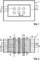
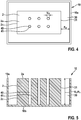
- Figs. 1 and 2 show an embodiment of a feedthrough connector 1 according to the present invention.
- the feedthrough connector 1 comprises an electrically insulating body 2 formed out of a glass, wherein the body 2 further comprises a front side 2a and a back side 2b that faces away from the front side 2a, wherein the body 2 further comprises a circumferential lateral side 2c extending from the front side 2a to the back side 2b of the body 2.
- the body / insulator 2 further comprises a plurality of through-openings 40, wherein each through-opening 40 extends from the front side 2a to the back side 2b of the body 2, and a corresponding plurality of electrical conductors 4, wherein each conductor 4 is arranged in one of the through-openings 40 such that the respective through-opening 40 is hermetically sealed.
- the respective conductor 4 comprises a metallic material, a first end 4a arranged at the front side 2a and connected to a first contact pad 5 arranged on the front side 2a, and an opposing second end 4b arranged at the back side 2b and connected to a second contact pad arranged 6 arranged on the back side 2b.
- the feedthrough connector 1 comprises a circumferential flange 3 comprising a further metallic material, wherein the flange 3 is connected to the lateral side 2c of the body 2 such that the flange 3 surrounds the body 2 and contacts the lateral side 2c of the body 2.
- the flange 3 can cover the entire lateral side 2c of the electrically insulating body 2 of the connector 1.
- the respective through-opening 40 of the connector 1 can comprise a first section 40a starting at the front side 2a of the body 2 and connected to a second section 40b extending to the back side 2b of the body 2 (cf. Fig.
- the first and the second section 40a, 40b of the respective through-opening 40 are arranged offset with respect to one another so that the respective through-opening 40 comprises a narrowing 401
- the flange 3 particularly covers a circumferential section 2cc of the lateral side 2c, which section 2cc comprises a height H cc corresponding to a length V 40a (in a direction perpendicular to the front side 2a and/or back side 2b) of the first section 40a of the respective through-opening 40 (cf. Fig. 26 ).
- the flange could extend along the entire length height V h of the wafer.
- the first and second contact pads 5, 6 as well as the flanges the metallic materials described herein can be used.
- first contact pads 5 on the front side 2a of the body 2 are configured to be arranged outside a housing 12 of an implantable medical implant device 11, and/or the second contact pads 6 on the back side 2b of the body 2 are configured to be connected to an electrical circuit 13 enclosed by said housing 12, which circuit can be arranged on a substrate 14 such as a printed circuit board.
- the feedthrough connector 1 thus provides electrical connection between said electrical circuit 13 and a component (such as a header) arranged outside said housing 12.
- the body 2 can comprise a height V h corresponding to a distance between the front side 2a and the back side 2b of the body 2 that is in the range from 0.3 mm to 1.5 mm.
- a minimal distance D m of the respective first contact pad 5 to an edge of the front side 2a of the body 2 is in the range from 0.25 mm to 1.0 mm.
- a minimal distance D' m of the respective second contact pad 6 to an edge of the back side 2b of the body 2 is in the range from 0.25 mm to 1.0 mm.
- the flange 3 can comprise a thickness F d in a direction normal to the lateral side 2c of the flange 3 that is in the range from 0.2 mm to 3.0 mm.
- the flange 3 comprises a height F h in a direction along which the respective conductor 4 extends between the front side 2a and the back side 2b of the body 2 (or in a direction perpendicular to the front side 2a and/or back side 2b of the body 2) that is in the range from 0.3 mm to 1.5 mm.
- the respective first contact pad 5 can comprise a thickness C h in a direction normal to the front side 2a of the body 2 that is in the range from 0.05 mm to 0.5 mm (cf. Fig. 2 ).
- the respective second contact pad 6 can comprise a thickness C'h in a direction normal to the back side 2b of the body 2 that is in the range from 0.05 mm to 0.5 mm (cf. Fig. 2 ).
- the respective first contact pad 5 can comprise a width C w in a direction parallel to the front side 2a of the body 2 that is in the range from 0.1 mm to 1 mm (cf. Fig. 2 ).
- the respective second contact pad 6 can comprise a width C' w in a direction parallel to the back side 2b of the body 2 that is in the range from 0.1 mm to 1 mm (cf. Fig. 2 ).
- the respective conductor 4 can comprise a length (e.g. in the direction of the height of the body 2) V h as indicated in Fig. 2 that is in the range from 0.5 mm to 1.5mm (corresponding e.g. to the height V h of the body 2 and of the flange 3).
- the respective conductor 4 can comprise a diameter V d , particularly perpendicular to the length V h of the respective conductor 4 or perpendicular to the height V h of the body 2 and/or flange 3 that is in the range from 0.01 mm to 0.5 mm.
- the feedthrough connector 1 shown in Fig. 1 and 2 can be produced using a method according to the present invention which shall be described in more detail below.
- a glass wafer 100 (e.g. circular wafer having diameter in the range from e.g. 100 mm to 300 mm) is provided as shown in Fig 3 , which comprises a plurality of adjacent wafer portions 10, wherein each wafer portion 10 comprises a front side 10a and a back side 10b facing away from the respective front side.
- the respective wafer portion 10 will form a body 2 of the respective final feedthrough connector 1 and will be provided with conductors 4, contact pads 5, 6 and a flange during the process.
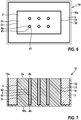
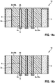
- blind holes 40 are formed in the front side 10a of the respective wafer portion 10 and a circumferential recess 30 such that the recess 30 surrounds said blind holes 40.
- the blind holes 40 and/or the recess 30 of the respective wafer portion 10 can have e.g. a depth V h in the range from 50% to 95% of the glass wafer's 100 height in a direction perpendicular to the respective front side 2a or back side 2b (see also above).
- a metallic material is arranged in the blind holes 40 of the respective wafer portion 10 to form conductors 4, so that each conductor 4 comprises a first end 4a at the front side 10a of the respective wafer portion 10 and a second end 4b at a bottom of the respective blind hole 40.
- a further metallic material is filled in the recess 30 of the respective wafer portion 10 to form a flange 3 of the respective wafer portion 10. This is indicated in Figs. 6 and 7 .
- the metallic material and the further metallic material can be identical.
- the blind holes 40 and/or the respective recess 30 in the front side 10a of the respective wafer portion 10 can be formed by patterning the front side 10a of the respective wafer portion 10 with a photoresist (PR) followed by a dry etching process such as e.g. RIE (reactive ion etching).
- RIE reactive ion etching
- ICP inductive coupled plasma
- said blind holes 40 and/or said recess 30 of the respective wafer portion 10 can also be formed using a laser.
- a coating 42 can be applied to an inner side 41 of the respective blind hole 40 of the respective wafer portion 10 before said metallic material is filled in the blind holes 40 of the respective wafer portion.
- a coating 32 can be applied to an inner side 31 of the recess 30 of the respective wafer portion 10 before said further metallic material is filled in the recess 30 of the respective wafer portion 10.
- the coating 42, 32 of the inner sides 41, 31 of the blind holes 40 or of the recesses 30 can be a metallization process.
- Such a metallization 42, 32 can comprise one or a combination of Ti, Ta, an alloy comprising Ti and W, Ni (e.g. in form of a Ni seed layer).
- the respective coating 42, 32 can be applied by way of suitable methods such as physical vapor deposition (PVD), sputtering, or evaporation.
- PVD physical vapor deposition
- the thickness of the respective coating/metallization 42, 32 can be in the range from e.g. 0.1 ⁇ m to 1 ⁇ m.
- blind holes 40 and/or the recess 30 of the respective wafer portion 10 can be filled (e.g. after applying the coatings 32, 42) with the respective metallic material by means of a CVD process (depositing of e.g. one of W, Ni, Ti), or by means of plating (e.g. Ni).
- CVD process depositing of e.g. one of W, Ni, Ti
- plating e.g. Ni
- the front side 10a of the respective wafer portion 10 can be planarized, if necessary, by way of suitable methods (e.g. CMP).
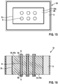
- the front side 10a of the respective wafer portion can be covered by means of a mask 50 as shown in Figs. 8 and 9 such that the first ends 4a of the conductors 4 at the front side 10a of the respective wafer portion 10 are not covered by the mask 50.
- a further metallic material can be deposited on the non-covered first ends 4a of the conductors 4 (through holes 51 of the mask 50) to form the first contact pads 5.
- the mask 50 can be removed from the front side 10a of the respective wafer portion 10 which now comprises the first contact pads 5 formed on the conductors 4 as shown in Figs.
- the first contact pads 5 can be formed out of a metal such as e.g. one or a combination of Au, Pt, Nb, Ti, that can be evaporated or sputtered onto the first ends 4a of the conductors 4 through the holes 51 in the mask 50.
- a metal such as e.g. one or a combination of Au, Pt, Nb, Ti, that can be evaporated or sputtered onto the first ends 4a of the conductors 4 through the holes 51 in the mask 50.
- a first variant of the method can be conducted, wherein a layer on the back side 10b of the respective wafer portion 10 is removed by back-grinding or CMP, as shown in Figs. 13a and 13b as well as Figs. 14a and 14b so as to expose the second ends 4b of the conductors 4 of the respective wafer portion 10.
- a plurality of holes 400 can be formed in the back side 10b of the respective wafer portion 10 instead, wherein each of said holes 400 is arranged offset with respect to an associated blind hole 40 formed in the front side 10a of the respective wafer portion (as described above), such that the respective hole 400 exposes a portion of the conductor 4 in the associated blind hole 40.
- the metallic material used for forming the conductors 4 is deposited in the newly formed holes 400 in the back side 10b of the respective wafer portion 10 to form a narrowing 401 of the respective conductor 4 and to prolong the respective conductor 4 such that it extends with its second end 4b up to the back side 10b of the respective wafer portion 10 as indicated in Fig. 27 .
- a coating can be applied to an inner side of the respective hole 400 (using e.g. one of the materials stated with respect to the coating 42 of the blind holes 40) before the metallic material is filled into the holes 400.
- a mask can be used as in case of the first contact pads 5.
- a mask is arranged on the back side 10b of the respective wafer portion 10 such that the second end 4b of the respective conductor at the back side 10b of the respective wafer portion 10 is not covered by the mask (not shown).
- a further metallic material is deposited on the non-covered second end 4b of the respective conductor 4 to form a second contact pad 6 thereon.
- the mask is removed from the back side 10b of the respective wafer portion 10.
- the further metallic material for the second contact pads 6 can comprise or can be formed by the materials stated above with respect to the second contact pads 6.
- this further metallic material can comprise or can be one of the following (e.g. solderable) metals: Sn/Ni, Cu/Ni , Sn/Pb, Pt, Rh, Nb, an alloy comprising Sn, Ag, and Cu.
- the glass waver 100 (i.e. the connected wafer portion 10) is mounted on a carrier 200 as shown in Fig. 17 , wherein particularly the front side 10a of the respective wafer portion 10 is arranged on the carrier 200.
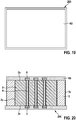
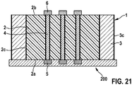
- exposing the flange and separation of the wafer portions 10 from one another can be conducted as shown in Figs. 18 to 21 by removing a region 10c of each wafer portion 10 that surrounds the flange 3 of the respective waver portion 10 so that a circumferential lateral side 3c of the flange 3 of the respective wafer portion 10 is exposed and the remaining portion 2 of the respective wafer portion 10 forms the electrically insulating body 2 of the respective feed through connector 1 resting on the carrier 200.
- a mask 60 can be arranged on the back side 10b of each carrier portion 10, which mask 60 extend on the back side 10b of the respective wafer portion 10 up to an outer edge of the flange 3 of the respective wafer portion 10 so that said region 10c of the respective wafer portion 10 is not covered by the mask 60.
- the mask's protective metal can be formed by Ni or Al metal layers highly selective to dry etch chemistry.
- conventional lithography can be used to deposit a mask such as SU8 on the back side 10b of the respective wafer portion 10.
- the region 10c of the respective wafer portion 10 is removed by way of etching using e.g. a RIE dry etching process.
- said region 10c of the respective wafer portion 10 can be removed by means of a laser to separate the wafer portions 10 / feedthrough connectors 1 from one another.
- a laser based singulation can be followed by a wet or dry chemical process to remove residual glass and expose the flange 3 of the respective wafer portion 10 / feedthrough connector 1.
- a corresponding plurality of feedthrough connectors 1 rest on the carrier 200 as indicated in Figs. 22 and 23 .
- the individual feedthrough connector 1 can now be mounted to a device such as an implantable medical device 11 as shown in Figs. 24 and 25 .
- the second contact pads 6 are connected, particularly welded or soldered, to corresponding contacts of an electrical circuit 13 of the medical device 11 which circuit can be arranged on a substrate 14 (e.g. printed circuit board).
- a substrate 14 e.g. printed circuit board
- the flange 3 of the feedthrough connector 1 is welded in a hermetically sealed fashion to a housing 12 of the medical device 11.
- the feedthrough connector now provided an hermetically sealed interface for making electrical connections to the circuit 13 via the first contact pads 5 being arranged outside of the housing.
- the implantable medical device 11 can be an implantable cardiac pacemaker and the feedthrough connector 1 can provide electrical connections to a header of the pacemaker 11.
Landscapes
- Engineering & Computer Science (AREA)
- Health & Medical Sciences (AREA)
- Power Engineering (AREA)
- Animal Behavior & Ethology (AREA)
- Radiology & Medical Imaging (AREA)
- Life Sciences & Earth Sciences (AREA)
- Nuclear Medicine, Radiotherapy & Molecular Imaging (AREA)
- General Health & Medical Sciences (AREA)
- Public Health (AREA)
- Veterinary Medicine (AREA)
- Biomedical Technology (AREA)
- Manufacturing & Machinery (AREA)
- Microelectronics & Electronic Packaging (AREA)
- Coupling Device And Connection With Printed Circuit (AREA)
- Container, Conveyance, Adherence, Positioning, Of Wafer (AREA)
Abstract
Description
- The present invention relates to a feedthrough connector, particularly for an implantable medical device, an implantable medical device, as well as to a method for producing a feedthrough connector.
- A hermetic feedthrough connector usually is an expensive component that requires high reliability. Such feedthroughs and interconnects are critical parts of implantable medical devices that provide an interface between the electronics inside a housing of the device and the outside system in the human body. Bio-compatibility and reliability are critical. Additionally with miniaturization these components it is desirable to shrink such components and to have them compatible with integration to next level assembly.
- Therefore, reliable low cost solutions are desired to produce feedthroughs which can meet these goals. Particularly, traditional pin type feedthroughs use Nb or Pt/Ir pins that are brazed (usually with Au) into a ceramic which in turn is Au brazed to a flange (usually Ti) that interfaces with the device's housing. Furthermore, feedthroughs can also be made with a HTCC (High Temperature Cofired Ceramic) technology that use Pt pastes applied to ceramic substrates and sequentially fired in a fashion similar to LTCC substrate manufacturing. However, standard pin based feedthroughs component miniaturization is limited. Furthermore, costs are high on standard pin feedthroughs due to labor content, while HTCC feedthroughs require many layers to achieve needed hermiticity (> 10) of the feedthrough.
- Based on the above, it is an object of the present invention to provide a reliable feedthrough connector that can be produced in a relatively easy fashion allowing miniaturization, simplicity and volume fabrication.
- This problem is solved by a feedthrough connector according to claim 1, a method for producing such a feedthrough connector, and an implantable medical device comprising a feedthrough connector according to the present invention.
- According to claim 1, a feedthrough connector is disclosed, comprising:
- an electrically insulating body formed out of a glass, the body comprising a front side and a back side facing away from the front side, wherein the body further comprises a circumferential lateral side extending from the front side to the back side of the body, and wherein the body comprises a plurality of through-openings, wherein each through-opening extends from the front side to the back side of the body,
- a plurality of electrical conductors (also denoted as TGVs for through glas vias), each conductor arranged in one of the through-openings to hermetically seal the respective through-opening, wherein the respective conductor comprises or is formed out of a metallic material, wherein the respective conductor further comprises a first end arranged at the front side and connected to a first contact pad arranged on the front side, and an opposing second end arranged at the back side and connected to a second contact pad arranged on the back side of the body, and
- a circumferential flange comprising or formed out of a metallic material, wherein the flange is connected to the lateral side of the body such that the flange surrounds the body and contacts the lateral side of the body.
- Advantageously, the design according to the present invention allows using standard manufacturing technologies using a glass-based substrate (e.g. wafer) to create reliable interconnecting feedthroughs.
- Particularly, according to an embodiment of the present invention, the flange covers a majority of the lateral side of the body. Particularly, the flange covers the lateral side of the body completely.
- Further, according to an embodiment of the present invention, the flange contacts said lateral side of the body in a hermetically sealed fashion.
- Furthermore, according to an embodiment of the present invention, the respective through-opening can comprise a first section starting at the front side of the body and connected to a second section of the respective through-opening extending to the back side of the body, wherein the first and the second section of the respective through opening are arranged offset with respect to one another so that the respective through-opening and the conductor arranged therein comprise a narrowing, wherein the flange particularly covers a circumferential section of the lateral side, which section comprises a height corresponding to a length (in a direction perpendicular to the front side of the body) of the first section of the respective through opening.
- Furthermore, according to an embodiment of the present invention, the body and/or the body together with the flange thereon forms a cuboid, particularly a rectangular cuboid. Particularly, the respective edge of the cuboid (e.g. rectangular cuboid) can also be rounded.
- Particularly, the flange is adapted such that it is weldable or brazeable to another component such as a housing of an implantable medical device.
- Particularly, according to an embodiment of the present invention, the feedthrough connector may comprise six through openings and corresponding conductors, wherein the conductors can be arranged in two parallel rows, each row comprising three conductors.
- Furthermore, according to an embodiment of the present invention, said glass is one of or comprises one of: SiO2, a borosilicate (e.g. the glass can be a borosilicate glass), a glass composition tailored to match the coefficient of thermal expansion (CTE) of the metallic material of the conductor and/or of the further metallic material of the flange.
- Further, according to an embodiment of the present invention, the metallic material comprised by or forming the respective conductor, is one of: Ti, Ta, Ni, W, an alloy comprising Ti and Al, an alloy comprising Ti and Ni, an alloy comprising Ti and W.
- Further, according to an embodiment of the present invention, the further metallic material comprised by or forming the flange is one of: Ti, Ta, Ni, W, an alloy comprising Ti and Al, an alloy comprising Ti and Ni, an alloy comprising Ti and W.
- Particularly, in an embodiment, the further metallic material of the flange is identical to the metallic material of the conductor, e.g. so as to minimize deposition steps (see also below).
- Furthermore, according to an embodiment of the present invention, the respective first contact pad arranged on the front side of the electrically insulating body comprises or is formed out of a further metallic material, wherein the further metallic material of the respective first contact pad is particularly one of: Au, Pt, Nb, Rh, Ti, an alloy comprising at least one of Au, Pt, Nb, Rh, Ti.
- Further, according to an embodiment of the present invention, the respective second contact pad arranged on the back side of the electrically insulating body comprises or is formed out of a further metallic material, wherein the further metallic material of the respective second contact pad is particularly one of: Sn/Ni; Ag; Au; an alloy comprising Sn, Ag, and Cu; an alloy comprising Sn and Pb. Sn/Ni is a metal bilayer where Ni is deposited first followed by Sn.
- Further, according to an embodiment of the present invention, the first contact pads on the front side of the body of the feedthrough connector are configured to be arranged outside a housing of an implantable medical implant device. Furthermore, in an embodiment, the second contact pads on the back side of the body of the feedthrough connector are configured to be connected to an electrical circuit enclosed by said housing. The feedthrough connector thus provides electrical connection between said electrical circuit and a component (such as a header) arranged outside said housing.
- Further, according to an embodiment of the present invention, the electrically insulating body of the feedthrough connector comprises a height corresponding to a distance between the front side and the back side of said body (e.g. in a direction along which the respective conductor extends between the front side and the back side of the body or in a direction perpendicular to the front side and/or the back side of the body) that is in the range from 0.5 mm to 1.5 mm.
- Further, according to an embodiment of the present invention, a minimal distance of the respective first contact pad to an edge of the front side of the body of the feedthrough connector is in the range from 0.25 mm to 1.0 mm. Further, in an embodiment, a minimal distance of the respective second contact pad to an edge of the back side of the body is in the range from 0.25 mm to 1.0 mm.
- Further, according to an embodiment of the present invention, the flange comprises a thickness in a direction perpendicular to the lateral side of the body of the feedthrough connector that is in the range from 0.2 mm to 3.0 mm.
- Further, according to an embodiment of the present invention, the flange comprises a height in a direction along which the respective conductor extends between the front side and the back side of the body (or in a direction perpendicular to the front side and/or the back side of the body of the feedthrough connector) that is in the range from 0.5 mm to 1.5 mm.
- Further, according to an embodiment of the present invention, each first or second contact pad can comprise a quadrangular or circular contact surface.
- Further, according to an embodiment of the present invention, the respective first contact pad can comprise a thickness in a direction perpendicular to the front side of the body that is in the range from 0.05 mm to 0.5 mm.
- Further, according to an embodiment of the present invention, the respective second contact pad can comprise a thickness in a direction perpendicular to the front side of the body of the feedthrough connector that is in the range from 0.05 mm to 0.5 mm.
- Further, according to an embodiment of the present invention, the respective first contact pad can comprise a width in a direction parallel to the front side of the body of the feedthrough connector that is in the range from 0.1 mm to 1 mm.
- Further, according to an embodiment of the present invention, the respective second contact pad can comprise a width in a direction parallel to the back side of the body of the feedthrough connector that is in the range from 0.1 mm to 1 mm.
- Further, according to an embodiment of the present invention, the respective conductor can comprise a length (e.g. in the direction of the height of the body of the feedthrough connector or in a direction perpendicular to the front side and/or to the back side of the body of the feedthrough connector) that is in the range from 0.5 mm to 1.5mm (corresponding e.g. to the height of the body and/or of the flange).
- Further, according to an embodiment of the present invention, the respective conductor can comprise a diameter (particularly in a direction parallel to the front side and/or to the back side of the body of the feedthrough connector, or in a direction perpendicular to the length of the respective conductor or perpendicular to the height of the body and/or of the flange) that is in the range from 0.01mm to 0.5mm.
- A further aspect of the present invention relates to a method for producing a feedthrough connector according to the present invention.
- Particularly, the method for producing the feedthrough connector comprises the steps of:
- providing a glass wafer (e.g. a circular wafer having diameter in the range from e.g. 100 mm to 300 mm) comprising a wafer portion or a plurality of wafer portions connected to each other, each wafer portion comprising a front side and a back side facing away from the respective front side,
- forming a plurality of blind holes and a circumferential recess in the front side of the respective wafer portion such that the recess surrounds said blind holes, and
- filling a metallic material in the blind holes of the respective wafer portion to form conductors, wherein each conductor comprises a first end at the front side of the respective wafer portion and a second end at a bottom of the respective blind hole, and
- filling a further metallic material in the recess of the respective wafer portion to form a flange of the respective wafer portion.
- According to an embodiment of the method according to the present invention, the metallic material of the conductors and the further metallic material of the flanges can be identical. The metallic materials already stated above may be used.
- Further, according to an embodiment of the method according to the present invention, the respective blind hole and/or the respective recess can be formed in the front side of the respective wafer portion by a patterning the front side of the respective wafer portion with a photoresist (PR) followed by a dry etching process such as e.g. RIE (reactive ion etching), or e.g. inductive coupled plasma (ICP) etch, or e.g. ion milling.
- Alternatively, a suitable Laser can be used to form said blind holes (holes do not break through to the back side of the body) and/or said recess into the front side of the respective wafer portion.
- Further, according to an embodiment of the method according to the present invention, the diameter of the respective through-opening or conductor perpendicular to the front side or back side of the respective wafer portion can be in the range from 0.01 mm to 0.5 mm, and the respective blind hole can have a depth in the range from 50% to 95 % of the glass wafer height in a direction perpendicular to the respective front side or back side of the wafer portion (see also above).
- As already mentioned above, the respective recess/flange can have a thickness in the range from 0.2mm to 3.0mm and a depth (height) of 50% to 95 % of said height of the glass wafer / respective wafer portion (see also above).
- Further, according to an embodiment of the method according to the present invention, a coating is applied to an inner side of the respective blind hole of the respective wafer portion before said metallic material is filled in the blind holes of the respective wafer portion, and/or wherein a coating is applied to an inner side of the recess of the respective wafer portion before said further metallic material is filled in the recess of the respective wafer portion.
- Further, according to an embodiment of the method according to the present invention, the coating of the inner sides of the blind holes or of the recesses can be a metallization. Particularly, the respective coating (e.g. metallization) acts as an adhesion layer. The coating can comprise one of Ti, Ta, an alloy comprising Ti and W, Ni (e.g. in form of a Ni seed layer). The respective coating can be applied through one of: physical vapor deposition (PVD), sputtering, evaporation.
- Further, according to an embodiment of the method according to the present invention, a thickness of the respective coating can be in the range from 0.1 µm to 1 µm.
- Further, according to an embodiment of the method according to the present invention, the blind holes and/or the recess of the respective wafer portion can be filled (e.g. after applying the coating) with the respective metallic material by means of a CVD process (depositing of e.g. one of W, Ni, Ti), or by means of plating (e.g. Ni).
- For both of these filling methods (plating or CVD), a chemical mechanical polish (CMP) can be applied afterward to the front side of the respective wafer portion to planarize the respective front side.
- Further, according to an embodiment of the method according to the present invention, the method further comprises the step of masking the front side of the respective wafer portion by a mask such that the first ends of the conductors at the front side of the respective wafer portion are left free by the mask, and wherein a further metallic material is deposited on the non-covered first ends of the conductors to form first contact pads thereon, and wherein the mask is removed from the front side of the respective wafer portion after forming of the first contact pads.
- Further, according to an embodiment of the method according to the present invention, the mask may be formed out of a thin metal or polymer foil with precise holes that are aligned on top of the front side of the respective wafer portion with the respective first ends of the conductors (i.e. with the positions of the blind holes on the front side of the respective waver portion).
- Further, according to an embodiment of the method according to the present invention, the further metallic material for the first contact pads can comprise or can be formed by the materials stated above with respect to the first contact pads. Particularly, a metal such as e.g. one of Au, Pt, Nb, Ti can be evaporated or sputtered onto the first ends of the conductors. The thickness (in a direction perpendicular to the front side of the respective wafer portion) of the respective first contact pad formed in this way can be in the range from 0.05 mm to 0.5 mm (see also above).
- Further, according to an embodiment of the method according to the present invention, the method further comprises the step of removing a layer on the back side of the respective wafer portion so as to expose the second ends of the conductors of the respective wafer portion.
- Further, according to an alternative embodiment of the method according to the present invention, the method further comprises the step of forming a plurality of holes in the back side of the respective wafer portion, wherein each of said holes is arranged offset (in a direction parallel to the back side of the body) with respect to an associated blind hole formed in the front side of the respective wafer portion, such that the respective hole exposes a portion of the conductor in the associated blind hole, and filling the metallic material into the holes in the back side of the respective wafer portion to form a narrowing of the respective conductor and to prolong the respective conductor such that it extends with its second end towards the back side of the respective wafer portion. Also here, a coating can be applied to an inner side of the respective hole formed in the back side of the respective wafer portion (using e.g. one of the materials stated above with respect to the coating of the blind holes) before the metallic material is filled into the holes to extend the conductors to the back side of the respective wafer portion. The narrowing of the conductor leads to a feedthrough that is particularly impermeable to liquids.
- Further, according to an embodiment of the method according to the present invention, the back side of the respective wafer portion is masked by a mask such that the second end of the respective conductor at the back side of the respective wafer portion is left free, and wherein a further metallic material is deposited on the non-covered second end of the respective conductor to form a second contact pad connected to the respective conductor, and wherein the mask is removed from the back side of the respective wafer portion after forming of the second contact pads.
- Further, according to an embodiment of the method according to the present invention, the further metallic material for the second contact pads can comprise or can be formed by the materials stated above with respect to the second contact pads.
- Particularly, the further metallic material can comprise or can be one of the following (e.g. solderable) metals: Sn/Ni, Cu/Ni, Sn/Pb, Pt, Rh, Nb, an alloy comprising Sn, Ag, and Cu.
- Further, according to an embodiment of the method according to the present invention, the method further comprises the steps of mounting the glass wafer on a carrier, wherein particularly the front side of the respective wafer portion is arranged on the carrier, i.e. faces towards the carrier.
- Further, according to an embodiment of the method according to the present invention, the method further comprises the step of removing a region of the wafer portion that surrounds the flange of the respective wafer portion so that a circumferential lateral side of the flange of the respective wafer portion is exposed and the respective wafer portion forms an electrically insulating body of a feed through connector resting on the carrier. When several wafer portions are attached to each other this step also leads to separating the wafer portions from one another.
- The method according to the invention therefore allows producing feedthroughs directly with an integrated flange. In previous methods, a flange had to be added separately after the production of the feedthrough element itself by for example brazing a metal flange to the glass insulator. The present method is therefore more efficient and less expensive than previous methods.
- Further, according to an embodiment of the method according to the present invention, before the step of removing a region of the wafer portion that surrounds the flange of the respective wafer portion (and thereby separating the wafer portions from one another when several wafer portions are present), a mask is arranged on the back side of the/each wafer portion, which mask extends on the back side of the respective wafer portion up to an outer edge of the flange of the respective waver portion so that said region of the respective wafer portion is not covered but left free for removal.
- Particularly, the mask (protective metal) can be formed by Ni or Al metal layers highly selective to dry etch chemistry for glass wafer. Alternatively, conventional lithography can be used to deposit a mask such as SU8 on the back side of the respective wafer portion.
- Further, according to an embodiment of the method according to the present invention, said region of the respective wafer portion is then removed by an etching process.
- Further, according to an embodiment of the method according to the present invention, a RIE dry etching process can be used to remove said region of the respective wafer portion.
- Alternatively, said region of the respective wafer portion can be removed by means of a laser to separate the wafer portion that surrounds the flange/the wafer portions/feedthrough connectors from one another.
- Particularly, such a laser-based separation can be followed by a wet or dry chemical process to remove residual glass and expose the flange of the respective wafer portion/feedthrough connector.
- An etching gas used in an etching process described above can be a fluorine-based plasma, particularly a C4F8 plasma, or CF4 plasma, or SF6.
- Furthermore, the respective mask can be removed by a wet or dry ash process (depending on material used for the respective mask).
- Furthermore, yet another aspect of the present invention relates to an implantable medical device comprising a feedthrough connector according to the present invention.
- According to an embodiment, the medical device comprises a housing that is welded to the flange of the feedthrough connector.
- Furthermore, according to an embodiment of the medical device, the first contact pads of the feedthrough connector are arranged outside the housing.
- Further, according to an embodiment of the medical device, the second contact pads of the feedthrough connector are arranged in an internal space enclosed by the housing. Particularly, the second contact pads can be connected to an electrical circuit of the medical device arranged in said internal space. Particularly, the electrical circuit can be arranged on a substrate arranged in said internal space. The substrate can be a printed circuit board.
- Particularly, the present invention using glass-based feedthroughs advantageously allows highly parallel processing of many feedthroughs by using glass wafers or panels with semiconductor-based processing equipment and process recipes. For example, a 200 mm glass wafer allows processing of upwards of 1000 feedthroughs in parallel. Thus, production costs can be significantly reduced. The technology further allows reduced pad to pad or contact to contact pitches as might be needed for Neurological implants that require a high I/O count therapy.
- Furthermore, in the following, embodiments of the present invention shall be described with reference to the Figures, wherein
- Fig. 1
- shows a schematical plan view onto a front side of a feedthrough connector according to the present invention;
- Fig. 2
- shows a schematical cross sectional view of the feedthrough connector shown in
Fig. 1 ; - Fig. 3
- shows a glass wafer that can be used to produce multiple feedthrough connectors of the kind shown in
Figs. 1 and 2 in a parallel fashion; - Fig. 4
- shows a schematical plan view onto a wafer portion of the glass wafer shown in
Fig. 3 after forming blind holes and a circumferential recess into a front side of the wafer portion; - Fig. 5
- shows a schematical cross sectional view of the wafer portion shown in
Fig. 4 ; - Fig. 6
- shows a schematical plan view onto the wafer portion of
Figs. 4 and 5 after filling of the blind holes and the recess with a metallic material to form conductors and a flange; - Fig. 7
- shows a schematical cross section view of the wafer portion shown in
Fig. 6 ; - Figs. 8 to 12
- show forming of first contact pads on the first ends of the conductors;
- Figs. 13 to 16
- show forming of second contact pads on the second ends of the conductors;
- Fig. 17
- shows mounting of the glass wafer onto a carrier;
- Figs. 18 to 21
- show the step of releasing the flanges and thereby separating of the individual feedthrough connectors;
- Figs. 22 to 23
- show the carrier with the separated feedthrough connectors arranged thereon;
- Figs. 24 to 25
- show connecting of a feedthrough connector to an electrical circuit and a housing of an implantable medical device; and
- Figs. 26 to 27
- show an alternative way of forming conductors in the respective wafer portion / electrically insulating body of the respective feedthrough connector.
-
Figs. 1 and 2 show an embodiment of a feedthrough connector 1 according to the present invention. The feedthrough connector 1 comprises an electrically insulatingbody 2 formed out of a glass, wherein thebody 2 further comprises afront side 2a and aback side 2b that faces away from thefront side 2a, wherein thebody 2 further comprises a circumferentiallateral side 2c extending from thefront side 2a to theback side 2b of thebody 2. The body /insulator 2 further comprises a plurality of through-openings 40, wherein each through-opening 40 extends from thefront side 2a to theback side 2b of thebody 2, and a corresponding plurality ofelectrical conductors 4, wherein eachconductor 4 is arranged in one of the through-openings 40 such that the respective through-opening 40 is hermetically sealed. Therespective conductor 4 comprises a metallic material, afirst end 4a arranged at thefront side 2a and connected to afirst contact pad 5 arranged on thefront side 2a, and an opposingsecond end 4b arranged at theback side 2b and connected to a second contact pad arranged 6 arranged on theback side 2b. Furthermore, the feedthrough connector 1 comprises acircumferential flange 3 comprising a further metallic material, wherein theflange 3 is connected to thelateral side 2c of thebody 2 such that theflange 3 surrounds thebody 2 and contacts thelateral side 2c of thebody 2. - As shown in
Fig. 2 , theflange 3 can cover the entirelateral side 2c of the electrically insulatingbody 2 of the connector 1. - According to an embodiment of the feedthrough connector 1 shown in
Figs. 26 and 27 (see also below), the respective through-opening 40 of the connector 1 can comprise afirst section 40a starting at thefront side 2a of thebody 2 and connected to asecond section 40b extending to theback side 2b of the body 2 (cf.Fig. 26 ), wherein the first and thesecond section flange 3 particularly covers a circumferential section 2cc of thelateral side 2c, which section 2cc comprises a height Hcc corresponding to a length V40a (in a direction perpendicular to thefront side 2a and/or backside 2b) of thefirst section 40a of the respective through-opening 40 (cf.Fig. 26 ). Alternatively however, the flange could extend along the entire length height Vh of the wafer. - For forming the
conductors 4, the first andsecond contact pads - Further, particularly, the
first contact pads 5 on thefront side 2a of thebody 2 are configured to be arranged outside ahousing 12 of an implantablemedical implant device 11, and/or thesecond contact pads 6 on theback side 2b of thebody 2 are configured to be connected to anelectrical circuit 13 enclosed by saidhousing 12, which circuit can be arranged on asubstrate 14 such as a printed circuit board. The feedthrough connector 1 thus provides electrical connection between saidelectrical circuit 13 and a component (such as a header) arranged outside saidhousing 12. - As indicated in
Fig. 2 , according to an embodiment of the present invention, thebody 2 can comprise a height Vh corresponding to a distance between thefront side 2a and theback side 2b of thebody 2 that is in the range from 0.3 mm to 1.5 mm. - Furthermore, as indicated in
Fig. 1 , according to an embodiment of the present invention, a minimal distance Dm of the respectivefirst contact pad 5 to an edge of thefront side 2a of thebody 2 is in the range from 0.25 mm to 1.0 mm. Further, according to an embodiment, a minimal distance D'm of the respectivesecond contact pad 6 to an edge of theback side 2b of thebody 2 is in the range from 0.25 mm to 1.0 mm. - Further, as indicated in
Fig. 2 , in an embodiment, theflange 3 can comprise a thickness Fd in a direction normal to thelateral side 2c of theflange 3 that is in the range from 0.2 mm to 3.0 mm. - Further, as indicated in
Fig. 5 , according to an embodiment, theflange 3 comprises a height Fh in a direction along which therespective conductor 4 extends between thefront side 2a and theback side 2b of the body 2 (or in a direction perpendicular to thefront side 2a and/or backside 2b of the body 2) that is in the range from 0.3 mm to 1.5 mm. - Furthermore, in an embodiment, the respective
first contact pad 5 can comprise a thickness Ch in a direction normal to thefront side 2a of thebody 2 that is in the range from 0.05 mm to 0.5 mm (cf.Fig. 2 ). Further, in an embodiment, the respectivesecond contact pad 6 can comprise a thickness C'h in a direction normal to theback side 2b of thebody 2 that is in the range from 0.05 mm to 0.5 mm (cf.Fig. 2 ). - Furthermore, in an embodiment, the respective
first contact pad 5 can comprise a width Cw in a direction parallel to thefront side 2a of thebody 2 that is in the range from 0.1 mm to 1 mm (cf.Fig. 2 ). Likewise, in an embodiment, the respectivesecond contact pad 6 can comprise a width C'w in a direction parallel to theback side 2b of thebody 2 that is in the range from 0.1 mm to 1 mm (cf.Fig. 2 ). - Furthermore, according to an embodiment, the
respective conductor 4 can comprise a length (e.g. in the direction of the height of the body 2) Vh as indicated inFig. 2 that is in the range from 0.5 mm to 1.5mm (corresponding e.g. to the height Vh of thebody 2 and of the flange 3). - Furthermore, in an embodiment, as indicated in
Fig. 4 , therespective conductor 4 can comprise a diameter Vd, particularly perpendicular to the length Vh of therespective conductor 4 or perpendicular to the height Vh of thebody 2 and/orflange 3 that is in the range from 0.01 mm to 0.5 mm. - Particularly, the individual dimensions of the feedthrough connector 1 stated above can be combined in any reasonable manner.
- Particularly, the feedthrough connector 1 shown in
Fig. 1 and 2 can be produced using a method according to the present invention which shall be described in more detail below. - According to the method, a glass wafer 100 (e.g. circular wafer having diameter in the range from e.g. 100 mm to 300 mm) is provided as shown in
Fig 3 , which comprises a plurality ofadjacent wafer portions 10, wherein eachwafer portion 10 comprises afront side 10a and aback side 10b facing away from the respective front side. - The
respective wafer portion 10 will form abody 2 of the respective final feedthrough connector 1 and will be provided withconductors 4,contact pads - As further indicated in
Figs. 4 and 5 a plurality ofblind holes 40 are formed in thefront side 10a of therespective wafer portion 10 and acircumferential recess 30 such that therecess 30 surrounds saidblind holes 40. Particularly, theblind holes 40 and/or therecess 30 of therespective wafer portion 10 can have e.g. a depth Vh in the range from 50% to 95% of the glass wafer's 100 height in a direction perpendicular to the respectivefront side 2a or backside 2b (see also above). - After forming of the
blind holes 40 /recess 30, a metallic material is arranged in theblind holes 40 of therespective wafer portion 10 to formconductors 4, so that eachconductor 4 comprises afirst end 4a at thefront side 10a of therespective wafer portion 10 and asecond end 4b at a bottom of the respectiveblind hole 40. A further metallic material is filled in therecess 30 of therespective wafer portion 10 to form aflange 3 of therespective wafer portion 10. This is indicated inFigs. 6 and 7 . Particularly, the metallic material and the further metallic material can be identical. - Particularly, the
blind holes 40 and/or therespective recess 30 in thefront side 10a of therespective wafer portion 10 can be formed by patterning thefront side 10a of therespective wafer portion 10 with a photoresist (PR) followed by a dry etching process such as e.g. RIE (reactive ion etching). Alternatively, inductive coupled plasma (ICP) or ion milling can be used. As a further alternative, saidblind holes 40 and/or saidrecess 30 of therespective wafer portion 10 can also be formed using a laser. - To improve adhesion of the metallic material filled into the blind hole or of the further metallic material filled into the recess of the
respective wafer portion 10, acoating 42 can be applied to aninner side 41 of the respectiveblind hole 40 of therespective wafer portion 10 before said metallic material is filled in theblind holes 40 of the respective wafer portion. Correspondingly, such acoating 32 can be applied to aninner side 31 of therecess 30 of therespective wafer portion 10 before said further metallic material is filled in therecess 30 of therespective wafer portion 10. Particularly, thecoating inner sides blind holes 40 or of therecesses 30 can be a metallization process. Such ametallization respective coating metallization - Furthermore, the
blind holes 40 and/or therecess 30 of therespective wafer portion 10 can be filled (e.g. after applying thecoatings 32, 42) with the respective metallic material by means of a CVD process (depositing of e.g. one of W, Ni, Ti), or by means of plating (e.g. Ni). - After filling of the
blind holes 40 /recess 30, thefront side 10a of therespective wafer portion 10 can be planarized, if necessary, by way of suitable methods (e.g. CMP). - In order to form
first contact pads 5 on thefront side 10a of therespective wafer portion 10, thefront side 10a of the respective wafer portion can be covered by means of amask 50 as shown inFigs. 8 and 9 such that the first ends 4a of theconductors 4 at thefront side 10a of therespective wafer portion 10 are not covered by themask 50. Then, as shown inFig. 10 a further metallic material can be deposited on the non-covered first ends 4a of the conductors 4 (throughholes 51 of the mask 50) to form thefirst contact pads 5. Afterwards, as shown inFig. 11 , themask 50 can be removed from thefront side 10a of therespective wafer portion 10 which now comprises thefirst contact pads 5 formed on theconductors 4 as shown inFigs. 11 and12 . Particularly, thefirst contact pads 5 can be formed out of a metal such as e.g. one or a combination of Au, Pt, Nb, Ti, that can be evaporated or sputtered onto the first ends 4a of theconductors 4 through theholes 51 in themask 50. - In order to also form second contact pads on the
back side 10b of therespective wafer portion 10, a first variant of the method can be conducted, wherein a layer on theback side 10b of therespective wafer portion 10 is removed by back-grinding or CMP, as shown inFigs. 13a and 13b as well asFigs. 14a and 14b so as to expose the second ends 4b of theconductors 4 of therespective wafer portion 10. - Alternatively, according to a second variant, which is shown in
Figs. 26 and 27 , a plurality ofholes 400 can be formed in theback side 10b of therespective wafer portion 10 instead, wherein each of saidholes 400 is arranged offset with respect to an associatedblind hole 40 formed in thefront side 10a of the respective wafer portion (as described above), such that therespective hole 400 exposes a portion of theconductor 4 in the associatedblind hole 40. Then, the metallic material used for forming theconductors 4 is deposited in the newly formedholes 400 in theback side 10b of therespective wafer portion 10 to form a narrowing 401 of therespective conductor 4 and to prolong therespective conductor 4 such that it extends with itssecond end 4b up to theback side 10b of therespective wafer portion 10 as indicated inFig. 27 . Also here, a coating can be applied to an inner side of the respective hole 400 (using e.g. one of the materials stated with respect to thecoating 42 of the blind holes 40) before the metallic material is filled into theholes 400. - Now, in order to form
second contact pads 6 on the second ends 4b of theconductors 4 as shown inFigs. 15 to 16 again a mask can be used as in case of thefirst contact pads 5. Also here, a mask is arranged on theback side 10b of therespective wafer portion 10 such that thesecond end 4b of the respective conductor at theback side 10b of therespective wafer portion 10 is not covered by the mask (not shown). Then, a further metallic material is deposited on the non-coveredsecond end 4b of therespective conductor 4 to form asecond contact pad 6 thereon. After forming of thesecond contact pads 6 the mask is removed from theback side 10b of therespective wafer portion 10. The further metallic material for thesecond contact pads 6 can comprise or can be formed by the materials stated above with respect to thesecond contact pads 6. Particularly, this further metallic material can comprise or can be one of the following (e.g. solderable) metals: Sn/Ni, Cu/Ni , Sn/Pb, Pt, Rh, Nb, an alloy comprising Sn, Ag, and Cu. - In order to separate the
individual wafer portions 10 from one another and exposing the flange so as to produce the final feedthrough connectors 1 each comprising an electrically insulatingbody 2 formed from therespective wafer portion 10, the glass waver 100 (i.e. the connected wafer portion 10) is mounted on acarrier 200 as shown inFig. 17 , wherein particularly thefront side 10a of therespective wafer portion 10 is arranged on thecarrier 200. - Particularly, exposing the flange and separation of the
wafer portions 10 from one another can be conducted as shown inFigs. 18 to 21 by removing aregion 10c of eachwafer portion 10 that surrounds theflange 3 of therespective waver portion 10 so that a circumferentiallateral side 3c of theflange 3 of therespective wafer portion 10 is exposed and the remainingportion 2 of therespective wafer portion 10 forms the electrically insulatingbody 2 of the respective feed through connector 1 resting on thecarrier 200. - Particularly, as shown in
Fig. 18 , for separating thewafer portions 10 from one another, amask 60 can be arranged on theback side 10b of eachcarrier portion 10, which mask 60 extend on theback side 10b of therespective wafer portion 10 up to an outer edge of theflange 3 of therespective wafer portion 10 so that saidregion 10c of therespective wafer portion 10 is not covered by themask 60. Particularly, the mask's protective metal can be formed by Ni or Al metal layers highly selective to dry etch chemistry. Alternatively, conventional lithography can be used to deposit a mask such as SU8 on theback side 10b of therespective wafer portion 10. - After positioning of the
mask 60, theregion 10c of therespective wafer portion 10 is removed by way of etching using e.g. a RIE dry etching process. Alternatively, saidregion 10c of therespective wafer portion 10 can be removed by means of a laser to separate thewafer portions 10 / feedthrough connectors 1 from one another. Particularly, such a laser based singulation can be followed by a wet or dry chemical process to remove residual glass and expose theflange 3 of therespective wafer portion 10 / feedthrough connector 1. - After separating the
individual wafer portions 10, a corresponding plurality of feedthrough connectors 1 rest on thecarrier 200 as indicated inFigs. 22 and 23 . The individual feedthrough connector 1 can now be mounted to a device such as an implantablemedical device 11 as shown inFigs. 24 and 25 . - Particularly, according to
Fig. 24 , thesecond contact pads 6 are connected, particularly welded or soldered, to corresponding contacts of anelectrical circuit 13 of themedical device 11 which circuit can be arranged on a substrate 14 (e.g. printed circuit board). - Furthermore, the
flange 3 of the feedthrough connector 1 is welded in a hermetically sealed fashion to ahousing 12 of themedical device 11. The feedthrough connector now provided an hermetically sealed interface for making electrical connections to thecircuit 13 via thefirst contact pads 5 being arranged outside of the housing. For instance, the implantablemedical device 11 can be an implantable cardiac pacemaker and the feedthrough connector 1 can provide electrical connections to a header of thepacemaker 11.
Claims (15)
- A feedthrough connector (1), comprising- an electrically insulating body (2) formed out of a glass, the body (2) comprising a front side (2a) and a back side (2b) facing away from the front side (2a), wherein the body (2) further comprises a circumferential lateral side (2c) extending from the front side (2a) to the back side (2b) of the body (2), and wherein the body (2) comprises a plurality of through-openings (40), wherein each through-opening (40) extends from the front side (2a) to the back side (2b) of the body (2),- a plurality of electrical conductors (4), each conductor (4) arranged in one of the through-openings (40) such that the respective through-opening (40) is hermetically sealed, wherein the respective conductor (4) comprises a metallic material, a first end (4a) arranged at the front side (2a) and connected to a first contact pad (5) arranged on the front side (2a), and an opposing second end (4b) arranged at the back side (2b) and connected to a second contact pad (6) arranged on the back side (2b), and- a circumferential flange (3) comprising a further metallic material, wherein the flange (3) is connected to the lateral side (2c) of the body (2) such that the flange (3) surrounds the body (2) and contacts the lateral side (2c) of the body (2).
- The feedthrough connector according to claim 1, wherein said glass is one of or comprises one of: SiO2, or a borosilicate.
- The feedthrough connector according to one of the preceding claims, wherein the metallic material of the respective conductor (4) is one of: Ti, Ta, Ni, W, Au, an alloy comprising Ti and Al, an alloy comprising Ti and Ni, an alloy comprising Ti and W.
- The feedthrough connector according to claim 1 or 2, wherein the further metallic material of the flange (3) is one of: Ti, Ta, Ni, W, Au an alloy comprising Ti and Al, an alloy comprising Ti and Ni, an alloy comprising Ti and W.
- The feedthrough connector according to one of the preceding claims, wherein the respective first contact pad (5) comprises or is formed out of a further metallic material, wherein the further metallic material of the respective first contact pad (5) is particularly one of: Au, Pt, Nb, Rh, Ti, an alloy comprising at least one of Au, Pt, Nb, Rh, Ti.
- The feedthrough connector according to one of the preceding claims, wherein the respective second contact pad (6) comprises or is formed out of a further metallic material, wherein the further metallic material of the respective second contact pad (6) is particularly one of: Sn/Ni; Ag; Au; an alloy comprising Sn, Ag, and Cu; an alloy comprising Sn and Pb.
- A method for producing a feedthrough connector (1), the method comprising the steps of:- providing a glass wafer (100) comprising a wafer portion (10) or a plurality of wafer portions (10) connected to each other, each wafer portion (10) comprising a front side (10a) and a back side (10b) facing away from the front side (10a),- forming a plurality of blind holes (40) and a circumferential recess (30) in the front side (10a) of the respective wafer portion (10) such that the recess (30) surrounds said blind holes (40), and- filling a metallic material in the blind holes (40) of the respective wafer portion (10) to form conductors (4), wherein each conductor (4) comprises a first end (4a) at the front side (10a) of the respective wafer portion (10) and a second end (4b) at a bottom of the respective blind hole (40), and- filling a further metallic material in the recess (30) of the respective wafer portion (10) to form a flange (3) of the respective wafer portion (10).
- The method according to claim 7, wherein a coating (42) is applied to an inner side (41) of the respective blind hole (40) of the respective wafer portion (10) before said metallic material is filled in the blind holes (40) of the respective wafer portion (10), and/or wherein a coating (32) is applied to an inner side (31) of the recess (30) of the respective wafer portion (10) before said further metallic material is filled in the recess (30) of the respective wafer portion (10).
- The method according to claim 7 or 8, further comprising the step of masking the front side (10a) of the respective wafer portion (10) by a mask (50) such that the first ends (4a) of the conductors (4) at the front side (10a) of the respective wafer portion (10) are not covered by the mask (50), and wherein a further metallic material is deposited on the non-covered first ends (4a) of the conductors (4) to form first contact pads (5), and wherein the mask (50) is removed from the front side (10a) of the respective wafer portion (10) after forming of the first contact pads (5).
- The method according to one of the claims 7 to 9, further comprising the step of removing a layer on the back side (10b) of the respective wafer portion (10) so as to expose the second ends (4b) of the conductors (4) of the respective wafer portion (10).
- The method according to one of the claims 7 to 9, further comprising the step of forming a plurality of holes (400) in the back side (10b) of the respective wafer portion (10), wherein each of said holes (400) is arranged offset with respect to an associated blind hole (40) formed in the front side (10a) of the respective wafer portion (10), such that the respective hole (400) exposes a portion of the conductor (4) in the associated blind hole (40), and filling the metallic material into the holes (400) in the back side (10b) of the respective wafer portion (10) to form a narrowing (401) of the respective conductor (4) and to prolong the respective conductor (4) such that it extends with its second end (4b) towards the back side (10b) of the respective wafer portion (10).
- The method according to claim 10 or 11, wherein the back side (10b) of the respective wafer portion (10) is masked by a mask such that the second end (4b) of the respective conductor (4) at the back side (10b) of the respective wafer portion (10) is not covered by the mask, and wherein a further metallic material is deposited on the non-covered second end (4b) of the respective conductor (4) to form a second contact pad (6) connected to the respective conductor (4), and wherein the mask is removed from the back side (10b) of the respective wafer portion (10) after forming of the second contact pads (6).
- The method according to one of the claims 7 to 12, further comprising the step of mounting the glass wafer (100) on a carrier (200), wherein particularly the front side (10a) of the respective wafer portion (10) is arranged on the carrier (200).
- The method according to one of the claims 7 to 13, further comprising the step of removing a region of the wafer portion (10) that surrounds the flange (3) of the respective wafer portion (10) so that a circumferential lateral side (3c) of the flange (3) of the respective wafer portion (10) is exposed and the remaining portion (2) of the respective wafer portion (10) forms an electrically insulating body (2) of the feed through connector (1) resting on the carrier (200).
- An implantable medical device (11) comprising a feedthrough connector (1) according to one of the claims 1 to 6 or a feedthrough connector (1) produced with the method according to one of the claims 7 to 14.
Applications Claiming Priority (1)
| Application Number | Priority Date | Filing Date | Title |
|---|---|---|---|
| US201862698997P | 2018-07-17 | 2018-07-17 |
Publications (1)
| Publication Number | Publication Date |
|---|---|
| EP3597266A1 true EP3597266A1 (en) | 2020-01-22 |
Family
ID=63914893
Family Applications (1)
| Application Number | Title | Priority Date | Filing Date |
|---|---|---|---|
| EP18201265.8A Withdrawn EP3597266A1 (en) | 2018-07-17 | 2018-10-18 | Feedthrough connectors in glass |
Country Status (2)
| Country | Link |
|---|---|
| US (1) | US11298555B2 (en) |
| EP (1) | EP3597266A1 (en) |
Families Citing this family (3)
| Publication number | Priority date | Publication date | Assignee | Title |
|---|---|---|---|---|
| EP3597266A1 (en) * | 2018-07-17 | 2020-01-22 | BIOTRONIK SE & Co. KG | Feedthrough connectors in glass |
| CN111355209A (en) * | 2020-03-10 | 2020-06-30 | 摩科斯新材料科技(苏州)有限公司 | Implantable ceramic feedthrough connector and method of making the same |
| WO2024127197A1 (en) * | 2022-12-12 | 2024-06-20 | Wyss Center For Bio And Neuro Engineering | Feedthrough for a medical device |
Citations (4)
| Publication number | Priority date | Publication date | Assignee | Title |
|---|---|---|---|---|
| US20070060970A1 (en) * | 2005-09-15 | 2007-03-15 | Burdon Jeremy W | Miniaturized co-fired electrical interconnects for implantable medical devices |
| US20110190885A1 (en) * | 2010-02-02 | 2011-08-04 | W. C. Heraeus Gmbh | Method for sintering electrical bushings |
| US20140360748A1 (en) * | 2011-09-01 | 2014-12-11 | Medtronic, Inc. | Feedthrough assembly including a capacitive filter array |
| US20150101841A1 (en) * | 2013-10-10 | 2015-04-16 | Medtronic, Inc. | Hermetic conductive feedthroughs for a semiconductor wafer |
Family Cites Families (6)
| Publication number | Priority date | Publication date | Assignee | Title |
|---|---|---|---|---|
| US5818002A (en) * | 1996-03-01 | 1998-10-06 | Cts Corporation | Pressure change warning switch |
| DE102010006689B4 (en) * | 2010-02-02 | 2013-04-18 | Heraeus Precious Metals Gmbh & Co. Kg | Method for producing an electrical feedthrough, electrical feedthrough and implantable device |
| DE102011009862B4 (en) * | 2011-01-31 | 2012-11-08 | Heraeus Precious Metals Gmbh & Co. Kg | Cermet-containing bushing with holding element for a medically implantable device |
| DE102011009867B4 (en) * | 2011-01-31 | 2013-09-05 | Heraeus Precious Metals Gmbh & Co. Kg | Ceramic bushing for a medically implantable device |
| US9403023B2 (en) * | 2013-08-07 | 2016-08-02 | Heraeus Deutschland GmbH & Co. KG | Method of forming feedthrough with integrated brazeless ferrule |
| EP3597266A1 (en) * | 2018-07-17 | 2020-01-22 | BIOTRONIK SE & Co. KG | Feedthrough connectors in glass |
-
2018
- 2018-10-18 EP EP18201265.8A patent/EP3597266A1/en not_active Withdrawn
-
2019
- 2019-07-17 US US16/514,012 patent/US11298555B2/en not_active Expired - Fee Related
Patent Citations (4)
| Publication number | Priority date | Publication date | Assignee | Title |
|---|---|---|---|---|
| US20070060970A1 (en) * | 2005-09-15 | 2007-03-15 | Burdon Jeremy W | Miniaturized co-fired electrical interconnects for implantable medical devices |
| US20110190885A1 (en) * | 2010-02-02 | 2011-08-04 | W. C. Heraeus Gmbh | Method for sintering electrical bushings |
| US20140360748A1 (en) * | 2011-09-01 | 2014-12-11 | Medtronic, Inc. | Feedthrough assembly including a capacitive filter array |
| US20150101841A1 (en) * | 2013-10-10 | 2015-04-16 | Medtronic, Inc. | Hermetic conductive feedthroughs for a semiconductor wafer |
Also Published As
| Publication number | Publication date |
|---|---|
| US20200023187A1 (en) | 2020-01-23 |
| US11298555B2 (en) | 2022-04-12 |
Similar Documents
| Publication | Publication Date | Title |
|---|---|---|
| US7514791B2 (en) | High reliability multilayer circuit substrates | |
| US20090098643A1 (en) | Multilayer circuit devices and manufacturing methods using electroplated sacrificial structures | |
| US8258635B2 (en) | Implantable microelectronic device and method of manufacture | |
| US8003513B2 (en) | Multilayer circuit devices and manufacturing methods using electroplated sacrificial structures | |
| US7094701B2 (en) | Manufacturing method of semiconductor device | |
| JP5004376B2 (en) | Thin plate-like ceramic having multilayer electrode and manufacturing method | |
| US20040043615A1 (en) | Manufacturing method of a semiconductor substrate provided with a through hole electrode | |
| US11298555B2 (en) | Feedthrough connectors in glass | |
| CN100415634C (en) | Electronic device with cover layer in cavity and manufacturing method thereof | |
| US8291824B1 (en) | Monolithic exploding foil initiator | |
| JP4354545B2 (en) | Conductive feedthrough for ceramic bodies and method of manufacturing the same | |
| EP3381050B1 (en) | Embedded metallic structures in glass | |
| US9048012B2 (en) | Method of fabricating high-density hermetic electrical feedthroughs | |
| JP2004031965A (en) | Capacitor for semiconductor device and method of manufacturing the same | |
| EP1734001B1 (en) | Method of packaging MEMS at wafer level | |
| JP6245086B2 (en) | Package and package manufacturing method | |
| JP6325346B2 (en) | Wiring board, electronic device and electronic module | |
| CA1282189C (en) | Use of adherent layer for filling contact holes for semiconductor devices |
Legal Events
| Date | Code | Title | Description |
|---|---|---|---|
| PUAI | Public reference made under article 153(3) epc to a published international application that has entered the european phase |
Free format text: ORIGINAL CODE: 0009012 |
|
| STAA | Information on the status of an ep patent application or granted ep patent |
Free format text: STATUS: THE APPLICATION HAS BEEN PUBLISHED |
|
| AK | Designated contracting states |
Kind code of ref document: A1 Designated state(s): AL AT BE BG CH CY CZ DE DK EE ES FI FR GB GR HR HU IE IS IT LI LT LU LV MC MK MT NL NO PL PT RO RS SE SI SK SM TR |
|
| AX | Request for extension of the european patent |
Extension state: BA ME |
|
| STAA | Information on the status of an ep patent application or granted ep patent |
Free format text: STATUS: REQUEST FOR EXAMINATION WAS MADE |
|
| 17P | Request for examination filed |
Effective date: 20200715 |
|
| RBV | Designated contracting states (corrected) |
Designated state(s): AL AT BE BG CH CY CZ DE DK EE ES FI FR GB GR HR HU IE IS IT LI LT LU LV MC MK MT NL NO PL PT RO RS SE SI SK SM TR |
|
| STAA | Information on the status of an ep patent application or granted ep patent |
Free format text: STATUS: EXAMINATION IS IN PROGRESS |
|
| 17Q | First examination report despatched |
Effective date: 20230419 |
|
| STAA | Information on the status of an ep patent application or granted ep patent |
Free format text: STATUS: THE APPLICATION IS DEEMED TO BE WITHDRAWN |
|
| 18D | Application deemed to be withdrawn |
Effective date: 20240801 |