EP3595416A1 - Control unit having press-fit structure - Google Patents
Control unit having press-fit structure Download PDFInfo
- Publication number
- EP3595416A1 EP3595416A1 EP17899708.6A EP17899708A EP3595416A1 EP 3595416 A1 EP3595416 A1 EP 3595416A1 EP 17899708 A EP17899708 A EP 17899708A EP 3595416 A1 EP3595416 A1 EP 3595416A1
- Authority
- EP
- European Patent Office
- Prior art keywords
- press
- fit
- hole
- terminal
- reduced
- Prior art date
- Legal status (The legal status is an assumption and is not a legal conclusion. Google has not performed a legal analysis and makes no representation as to the accuracy of the status listed.)
- Granted
Links
Images


Classifications
-
- H—ELECTRICITY
- H01—ELECTRIC ELEMENTS
- H01R—ELECTRICALLY-CONDUCTIVE CONNECTIONS; STRUCTURAL ASSOCIATIONS OF A PLURALITY OF MUTUALLY-INSULATED ELECTRICAL CONNECTING ELEMENTS; COUPLING DEVICES; CURRENT COLLECTORS
- H01R13/00—Details of coupling devices of the kinds covered by groups H01R12/70 or H01R24/00 - H01R33/00
- H01R13/62—Means for facilitating engagement or disengagement of coupling parts or for holding them in engagement
- H01R13/629—Additional means for facilitating engagement or disengagement of coupling parts, e.g. aligning or guiding means, levers, gas pressure electrical locking indicators, manufacturing tolerances
- H01R13/631—Additional means for facilitating engagement or disengagement of coupling parts, e.g. aligning or guiding means, levers, gas pressure electrical locking indicators, manufacturing tolerances for engagement only
-
- H—ELECTRICITY
- H01—ELECTRIC ELEMENTS
- H01R—ELECTRICALLY-CONDUCTIVE CONNECTIONS; STRUCTURAL ASSOCIATIONS OF A PLURALITY OF MUTUALLY-INSULATED ELECTRICAL CONNECTING ELEMENTS; COUPLING DEVICES; CURRENT COLLECTORS
- H01R12/00—Structural associations of a plurality of mutually-insulated electrical connecting elements, specially adapted for printed circuits, e.g. printed circuit boards [PCB], flat or ribbon cables, or like generally planar structures, e.g. terminal strips, terminal blocks; Coupling devices specially adapted for printed circuits, flat or ribbon cables, or like generally planar structures; Terminals specially adapted for contact with, or insertion into, printed circuits, flat or ribbon cables, or like generally planar structures
- H01R12/50—Fixed connections
- H01R12/51—Fixed connections for rigid printed circuits or like structures
- H01R12/55—Fixed connections for rigid printed circuits or like structures characterised by the terminals
- H01R12/58—Fixed connections for rigid printed circuits or like structures characterised by the terminals terminals for insertion into holes
- H01R12/585—Terminals having a press fit or a compliant portion and a shank passing through a hole in the printed circuit board
-
- H—ELECTRICITY
- H01—ELECTRIC ELEMENTS
- H01R—ELECTRICALLY-CONDUCTIVE CONNECTIONS; STRUCTURAL ASSOCIATIONS OF A PLURALITY OF MUTUALLY-INSULATED ELECTRICAL CONNECTING ELEMENTS; COUPLING DEVICES; CURRENT COLLECTORS
- H01R12/00—Structural associations of a plurality of mutually-insulated electrical connecting elements, specially adapted for printed circuits, e.g. printed circuit boards [PCB], flat or ribbon cables, or like generally planar structures, e.g. terminal strips, terminal blocks; Coupling devices specially adapted for printed circuits, flat or ribbon cables, or like generally planar structures; Terminals specially adapted for contact with, or insertion into, printed circuits, flat or ribbon cables, or like generally planar structures
- H01R12/50—Fixed connections
- H01R12/51—Fixed connections for rigid printed circuits or like structures
- H01R12/55—Fixed connections for rigid printed circuits or like structures characterised by the terminals
-
- H—ELECTRICITY
- H05—ELECTRIC TECHNIQUES NOT OTHERWISE PROVIDED FOR
- H05K—PRINTED CIRCUITS; CASINGS OR CONSTRUCTIONAL DETAILS OF ELECTRIC APPARATUS; MANUFACTURE OF ASSEMBLAGES OF ELECTRICAL COMPONENTS
- H05K1/00—Printed circuits
- H05K1/18—Printed circuits structurally associated with non-printed electric components
-
- H—ELECTRICITY
- H01—ELECTRIC ELEMENTS
- H01R—ELECTRICALLY-CONDUCTIVE CONNECTIONS; STRUCTURAL ASSOCIATIONS OF A PLURALITY OF MUTUALLY-INSULATED ELECTRICAL CONNECTING ELEMENTS; COUPLING DEVICES; CURRENT COLLECTORS
- H01R12/00—Structural associations of a plurality of mutually-insulated electrical connecting elements, specially adapted for printed circuits, e.g. printed circuit boards [PCB], flat or ribbon cables, or like generally planar structures, e.g. terminal strips, terminal blocks; Coupling devices specially adapted for printed circuits, flat or ribbon cables, or like generally planar structures; Terminals specially adapted for contact with, or insertion into, printed circuits, flat or ribbon cables, or like generally planar structures
- H01R12/50—Fixed connections
- H01R12/51—Fixed connections for rigid printed circuits or like structures
-
- H—ELECTRICITY
- H01—ELECTRIC ELEMENTS
- H01R—ELECTRICALLY-CONDUCTIVE CONNECTIONS; STRUCTURAL ASSOCIATIONS OF A PLURALITY OF MUTUALLY-INSULATED ELECTRICAL CONNECTING ELEMENTS; COUPLING DEVICES; CURRENT COLLECTORS
- H01R13/00—Details of coupling devices of the kinds covered by groups H01R12/70 or H01R24/00 - H01R33/00
- H01R13/40—Securing contact members in or to a base or case; Insulating of contact members
- H01R13/405—Securing in non-demountable manner, e.g. moulding, riveting
- H01R13/41—Securing in non-demountable manner, e.g. moulding, riveting by frictional grip in grommet, panel or base
-
- H—ELECTRICITY
- H05—ELECTRIC TECHNIQUES NOT OTHERWISE PROVIDED FOR
- H05K—PRINTED CIRCUITS; CASINGS OR CONSTRUCTIONAL DETAILS OF ELECTRIC APPARATUS; MANUFACTURE OF ASSEMBLAGES OF ELECTRICAL COMPONENTS
- H05K2201/00—Indexing scheme relating to printed circuits covered by H05K1/00
- H05K2201/10—Details of components or other objects attached to or integrated in a printed circuit board
- H05K2201/10431—Details of mounted components
- H05K2201/1059—Connections made by press-fit insertion
Definitions
- the present invention relates to a press-fit terminal and an insertion guide for the press-fit terminal of a control unit having a press-fit structure.
- press-fit terminals as a technology for connecting, for example, a wiring substrate including circuit substrates or bus bars to terminals of a connector.
- the press-fit terminals include tip end portions each having a shape to be press-fitted.
- the tip end portions are press-fitted into conductive insertion holes formed in the wiring substrate to electrically and mechanically connect the terminals to the substrate, and the terminals to the bus bars.
- Related-art press-fit terminals include tip end portions each having an O-shape to be inserted into an insertion hole (for example, see Patent Literatures 1 and 2).
- the electronic control device disclosed in Patent Literature 1 includes a connector assembly body including a plurality of press-fit terminals, and a circuit substrate having a plurality of through holes. Further, the plurality of press-fit terminals are press-fitted into the plurality of through holes so that the connector assembly body is assembled to the circuit substrate. Accordingly, it has been difficult to align positions of the tip ends of the plurality of press-fit terminals with positions of the plurality of through holes.
- the present invention has been made to solve the above-mentioned problem, and provides a control unit having a press-fit structure capable of simplifying positioning of a plurality of press-fit terminals and a plurality of through holes formed in a substrate, and of improving ease of assembly.
- a control unit having a press-fit structure
- the control unit including a connector assembly body and a wiring substrate assembled to each other, the connector assembly body including: a conductive terminal; and a press-fit terminal formed at a tip end of the conductive terminal, the wiring substrate including: a connected portion to which the press-fit terminal is connected; and a guide portion extending from the wiring substrate around the connected portion, the press-fit terminal including: a tip end portion; a contact portion adjacent to the tip end portion; and a first enlarged portion formed on the conductive terminal side of the contact portion, the guide portion including: an opening portion opening in a direction in which the press-fit terminal is inserted; a guide hole extending from the opening portion to the wiring substrate; a tapered surface, which is formed on an inner side of the opening portion, and has an inner dimension decreasing as separating away from the opening portion; and a reduced-hole portion formed continuous to the tapered surface, the tip end portion of the press-fit terminal being configured such that the contact
- the respective guide portions are formed for the respective connected portions of the wiring substrate to which the plurality of press-fit terminals of the connector assembly body are connected. Further, the tip end portion of each press-fit terminal is guided by the guide portion into each connected portion of the wiring substrate.
- control unit having a press-fit structure according to exemplary embodiments of the present invention is described.
- FIG. 1 is a sectional view of a control device having a press-fit structure according to a first embodiment of the present invention for illustrating a state in which a connector assembly body 1 is assembled to a wiring substrate 2 as viewed from a front side of the control device.
- FIG. 2 is a sectional view for illustrating the state in which the connector assembly body is assembled to the wiring substrate as viewed from a side of the control device.
- the control device according to the first embodiment includes the connector assembly body 1 and the wiring substrate 2.
- the connector assembly body 1 includes a plurality of terminals 3 coupled to the connector assembly body 1 by, for example, insert molding.
- One end side of each terminal 3 protrudes from the connector assembly body 1, and is formed as a connector terminal to be connected to a connector (not shown) of the control device. Meanwhile, another end side thereof of each terminal 3 protrudes from the connector assembly body 1 to a side opposite to the one end side, and a press-fit terminal 10 is formed thereon.
- the terminals 3 and the press-fit terminals 10 are formed of metal plates such as copper plates, which are formed by being cut and bent and each have a rectangular cross-section. In FIG. 1 , only two terminals 3 are illustrated. However, the number of terminals 3 is not limited to two.
- the wiring substrate 2 is made of an insulating resin. Further, the wiring substrate 2 includes a plurality of bus bars 30 and 31 formed of, for example, copper plates by insert molding or the like. The bus bars 30 and 31 are branched off in the wiring substrate 2 to form a plurality of bus bar terminals 30A and 31A protruding from the wiring substrate 2. The bus bars 30 and 31 are bent to form the bus bar terminals 30A and 31A, and the bus bar terminals 30A and 31A each have a rectangular cross-section.
- the wiring substrate 2 includes a guide portion 20 extending from the wiring substrate 2.
- the guide portion 20 includes opening portions 20A and guide holes 20C.
- the opening portions 20A open in a direction in which the press-fit terminals 10 are inserted.
- the guide holes 20C extend from the opening portions 20A to the wiring substrate 2.
- the bus bar terminals 30A and 31A each protrude in the guide holes 20C.
- the guide portion 20 illustrated in FIG. 1 is molded integrally with the wiring substrate 2, but may be a separate member to be coupled.
- the press-fit terminals 10 are inserted into the guide holes 20C of the guide portion 20 to be connected to the bus bar terminals 30A and 31A of the wiring substrate 2.
- the connector assembly body 1 is electrically connected to the wiring substrate 2 through intermediation of the terminals 3, the press-fit terminals 10, the bus bar terminals 30A and 31A, and the bus bars 30 and 31.
- a tapered surface 20S is formed to have an inner dimension decreasing as separating away from the opening portion 20A.
- a reduced-hole portion 20B is formed starting from the tapered surface 20S to a bottom portion of the guide hole 20C.
- each press-fit terminal 10 On the terminal 3 side of each press-fit terminal 10, an enlarged portion 10C is formed to have a width larger than that of a tip end portion 10A. Further, a notched portion 10B is formed in the tip end portion 10A of the press-fit terminal 10. The bus bar terminals 30A and 31A are press-fitted into the notched portions 10B to be electrically and mechanically connected to the press-fit terminals 10.
- the tip end portions 10A of the press-fit terminals 10 are connected to the bus bar terminals 30A and 31A so that both surfaces of the press-fit terminals 10 and the bus bar terminals 30A and 31A are arranged orthogonal to each other.
- positional shift of the press-fit terminals 10 in a width direction of the bus bar terminals 30A and 31A is allowed within a width of the bus bar terminals 30A and 31A.
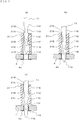
- FIG. 3A to FIG. 3D are views for illustrating processes for assembling the press-fit terminals according to the first embodiment to the wiring substrate.
- FIG. 3A is a view for illustrating a state before assembling the connector assembly body 1 to the wiring substrate 2.
- the tip end portion 10A of each press-fit terminal 10 of the connector assembly body 1 is positioned in each opening portion 20A of the guide portion 20 of the wiring substrate 2.
- the plurality of press-fit terminals 10 of the connector assembly body 1 are arranged to correspond to positions of the opening portions 20A of the guide portion 20 of the wiring substrate 2, respectively. Accordingly, when there is no abnormality such as large bend or deformation in each press-fit terminal 10, as illustrated in FIG. 3A , the tip end portion 10A of each press-fit terminal 10 is positioned in a vicinity of a center of each opening portion 20A of the guide portion 20.
- the press-fit terminals 10 are determined to have abnormality such as large bend or deformation. To detect such abnormality, when the press-fit terminals 10 are inserted into the guide portion 20, it is preferred to monitor a force applied to the press-fit terminals 10.
- a reaction force is measured, which is applied from the guide portion 20 to the press-fit terminals 10. Then, based on the measured values of the pressure sensor at a normal time and at an abnormal time, a threshold value is set for the measured values, thereby being capable of detecting abnormality.
- a threshold value is set for the measured values, thereby being capable of detecting abnormality.
- FIG. 3B is a view for illustrating a state in which the tip end portion 10A of each press-fit terminal 10 is inserted into the reduced-hole portion 20B of the guide portion 20.
- a position of each press-fit terminal 10 may vary within a machining tolerance of the press-fit terminal 10 and amounting tolerance to the connector assembly body 1, even when there is no abnormality such as large bend or deformation in each press-fit terminal 10.
- the tip end portions 10A or enlarged portions 10C of the press-fit terminals 10 may be brought into contact with the tapered surfaces 20S.
- the tip end portions 10A or the enlarged portions 10C in contact with the tapered surfaces 20S are moved along the tapered surfaces 20S to be guided to the reduced-hole portions 20B.
- FIG. 3C is a view for illustrating a state in which the press-fit terminals 10 are further inserted, and the tip end portions 10A of the press-fit terminals 10 have reached vicinities of tip ends of the bus bar terminals 30A and 31A.
- FIG. 3C when the enlarged portions 10C of the press-fit terminals 10 are brought into contact with the reduced-hole portions 20B of the guide portion 20, insertion resistance of the press-fit terminals 10 is increased.
- FIG. 3D is a view for illustrating a state in which the press-fit terminals 10 are further inserted from the state of FIG. 3C , and the bus bar terminals 30A and 31A are press-fitted into the notched portions 10B.
- the insertion resistance of the press-fit terminals 10 is further increased from the state of FIG. 3C .
- reduced portions 10D are formed in the press-fit terminals 10.
- the reduced portions 10D are formed from the enlarged portions 10C of the press-fit terminals 10 toward the terminals 3 side. Further, the reduced portions 10D are formed such that, when the tip end portions 10A of the press-fit terminals 10 reach the vicinities of the tip ends of the bus bar terminals 30A and 31A, boundaries 10P between the enlarged portions 10C and the reduced portions 10D approximately match with positions of boundaries 20P between the tapered surfaces 20S and the reduced-hole portions 20B.
- the insertion resistance is gradually increased. Meanwhile, when the tip end portions 10A collide with the bus bar terminals 30A and 31A, the insertion resistance is sharply increased. Further, when the tip end portions 10A are bent largely or are missing, the tip end portions 10A are not brought into contact with the bus bar terminals 30A and 31A, and hence the insertion resistance is not changed. Therefore, the abnormality of the press-fit terminals 10 can be detected based on the amount of change in insertion resistance.
- the plurality of press-fit terminals 10 of the connector assembly body 1 include the tip end portions 10A, the notched portions 10B, the enlarged portions 10C, and the reduced portions 10D.
- the guide portion 20 of the wiring substrate 2 includes the opening portions 20A each including the tapered surface 20S, and the reduced-hole portions 20B. Further, when the tip end portions 10A or the enlarged portions 10C are brought into contact with the tapered surfaces 20S due to positional shift of the press-fit terminals 10, the tip end portions 10A or the enlarged portions 10C are moved along the tapered surfaces 20S to be guided to the reduced-hole portions 20B.
- the tip end portions 10A of the press-fit terminals 10 can reach the bus bar terminals 30A and 31A.
- the positioning of the press-fit terminals 10 to the bus bar terminals 30A and 31A can easily be performed, to thereby improve ease of assembly of the connector assembly body 1 and the wiring substrate 2.
- the control device is configured such that the guide portion 20 is formed on the wiring substrate 2, and when the connector assembly body 1 is assembled to the wiring substrate 2, the press-fit terminals 10 reach the bus bar terminals 30A and 31A through the guide portion 20. Further, when there is abnormality such as large bend or deformation in the press-fit terminals 10, the press-fit terminals 10 are brought into contact with the guide portion 20 before being brought into contact with the bus bar terminals 30A and 31A. With this configuration, abnormality of the press-fit terminals 10 can be detected before the press-fit terminals 10 are brought into contact with the bus bar terminals 30A and 31A. Consequently, the bus bar terminals 30A and 31A can be prevented from being deformed and damaged due to collision of abnormal press-fit terminals 10 against the bus bar terminals 30A and 31A.
- the reduced portions 10D are formed to be continuous to the enlarged portions 10C of the press-fit terminals 10.
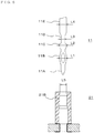
- FIG. 4 is a view of the control device having a press-fit structure according to a second embodiment of the present invention for illustrating a state in which a press-fit terminal 11 is assembled to a circuit substrate 4.
- FIG. 5 is a sectional view taken along the line V-V of FIG. 4 .
- FIG. 6 is a view for illustrating a relationship between a size of each portion of the press-fit terminal 11 and a size of a reduced-hole portion 21B of a guide portion 21.
- FIG. 7A to FIG. 7C are sectional views for illustrating processes for assembling the press-fit terminal 11 to the circuit substrate 4.
- the control device having a press-fit structure according to the second embodiment is different from the first embodiment in a shape of the press-fit terminal 11 and a shape of the guide portion 21. Further, the second embodiment is different from the first embodiment in that the connector assembly body 1 is assembled to the circuit substrate 4 in the second embodiment, whereas the connector assembly body 1 is assembled to the wiring substrate 2 in the first embodiment. Other structures are the same as those of the first embodiment.
- FIG. 4 only one press-fit terminal 11 of a plurality of press-fit terminals 11 included in the connector assembly body 1 is illustrated, but a shape of other press-fit terminals 11 is the same as that of the press-fit terminal 11 of FIG. 4 .
- the terminal 3 (not shown) of the connector assembly body 1 is formed on one end side of the press-fit terminal 11.
- the circuit substrate 4 is supported by support portions 100A and 100B.
- the support portions 100A and 100B are configured to prevent the circuit substrate 4 from being deformed and damaged when the press-fit terminal 11 is inserted into the circuit substrate 4.
- a wiring pattern (not shown) is formed on the circuit substrate 4 on which electronic components are mounted.
- insertion holes 40 are formed in the circuit substrate 4 as the same number as the plurality of press-fit terminals 11 included in the connector assembly body 1.
- a conductive portion 41 subjected to plating treatment is formed in each of the plurality of insertion holes 40.
- the guide portion 21 formed by molding an insulating resin is mounted to the circuit substrate 4. Further, a guide hole 21D passing through the guide portion 21 is formed in the guide portion 21.
- the press-fit terminal 11 is press-fitted into the insertion hole 40 of the circuit substrate 4 through the guide hole 21D.
- the guide portion 21 includes a leg portion 21E for positioning on the circuit substrate 4.
- the leg portion 21E is a rib, which is formed into an arc shape and extends from the guide portion 21.
- the circuit substrate 4 has a positioning hole 42.
- the guide portion 21 is positioned on the circuit substrate 4 through insertion of the leg portion 21E into the positioning hole 42 of the circuit substrate 4. After that, a center of the guide hole 21D is positioned so as to be aligned with a center of the insertion hole 40 through positioning of the guide portion 21 with respect to the circuit substrate 4.
- the press-fit terminal 11 includes a tip end portion 11A having a tapered-of f shape, an elastic leg portion 11B, a first enlarged portion 11C, a reduced portion 11D, and a second enlarged portion 11E.
- the press-fit terminal 11 is formed of a metal plate such as copper, which is formed by being cut and bent and has a rectangular cross-section.
- the elastic leg portion 11B is formed around a hole 11F passing through in a direction perpendicular to a longitudinal direction of the press-fit terminal 11.
- the hole 11F of the elastic leg portion 11B is elastically deformed when the press-fit terminal 11 is press-fitted into the insertion hole 40 of the circuit substrate 4, and is electrically and mechanically connected to an inner wall of the insertion hole 40.
- the guide hole 21D of the guide portion 21 includes an opening portion 21A, a reduced-hole portion 21B, and an enlarged-hole portion 21C.
- the opening portion 21A has an elliptical cross-sectional shape.
- the reduced-hole portion 21B has a rectangular cross-sectional shape conforming to the cross-sectional shape of the press-fit terminal 11.
- the enlarged-hole portion 21C has an elliptical cross-sectional shape. In the reduced-hole portion 21B, it is not always required that entire circumferences of the first enlarged portion 11C and the second enlarged portion 11E of the press-fit terminal 11 be in contact with the inner wall of the reduced-hole portion 21B.
- the cross-sectional shape of the reduced-hole portion 21B may have a relationship of size such that at least one side surface of both the side surfaces of the first enlarged portion 11C and the second enlarged portion 11E is brought into contact with the inner wall.
- Cross-sectional shapes of the opening portion 21A and the enlarged-hole portion 21C are not limited to an elliptical shape, but may be a rectangular shape, a circular shape, or an elongated circular shape.
- a maximum width of the elastic leg portion 11B of the press-fit terminal 11 is represented by L1
- a maximum width of the first enlarged portion 11C is represented by L2
- a width of the reduced portion 11D is represented by L3
- a maximum width of the second enlarged portion 11E is represented by L4, there is a relationship of L2 ⁇ L4>L1>L3 among L1 to L4.
- an inner dimension of the guide hole 21D has a smallest inner dimension L5 at the reduced-hole portion 21B.
- the reduced-hole portion 21B has a rectangular cross-sectional shape as illustrated in FIG. 5 , and hence the inner dimension L5 of the reduced-hole portion 21B refers to a long side of the reduced-hole portion 21B in cross-section.
- the inner dimension L5 of the reduced-hole portion 21B is set to a size which allows the first enlarged portion 11C and the second enlarged portion 11E of the press-fit terminal 11 to pass through the reduced-hole portion 21B.
- FIG. 7A is a view for illustrating a state in which the press-fit terminal 11 is inserted into the guide hole 21D, and the tip end portion 11A of the press-fit terminal 11 reaches a front of the insertion hole 40 of the circuit substrate 4.
- a tapered surface 21S is formed in the opening portion 21A of the guide hole 21D similarly to the guide hole 20C of the first embodiment.
- the width L3 of the reduced portion 11D of the press-fit terminal 11 is set to be smaller than widths of other portions of the press-fit terminal 11, and the reduced portion 11D is easily deformed.
- the reduced portion 11D is deformed so that the tip end portion 11A and the first enlarged portion 11C are moved along the tapered surface 21S. Further, the tip end portion 11A is guided to a vicinity of the center of the insertion hole 40 of the circuit substrate 4.
- FIG. 7B is a view for illustrating a state in which the press-fit terminal 11 is further inserted.
- the first enlarged portion 11C passes through the reduced-hole portion 21B, and the second enlarged portion 11E reaches the opening portion 21A.
- the tip end portion 11A passes through the insertion hole 40 of the circuit substrate 4.
- a contact area between the press-fit terminal 11 and an inner wall of the guide hole 21D is smallest, and the insertion resistance of the press-fit terminal 11 becomes smallest.
- FIG. 7C is a view for illustrating a state in which the press-fit terminal 11 is further inserted and is connected to the circuit substrate 4.
- the second enlarged portion 11E is positioned on the reduced-hole portion 21B, and the elastic leg portion 11B is inserted into the insertion hole 40 of the circuit substrate 4. Consequently, the press-fit terminal 11 is electrically and mechanically connected to the circuit substrate 4.
- the reduced portion 11D has an effect of absorbing vibration of the control device by being deformed.
- the press-fit terminal 11 includes the tip end portion 11A, the elastic leg portion 11B, the first enlarged portion 11C, the reduced portion 11D, and the second enlarged portion 11E. Further, the guide portion 21 having the guide hole 21D is mounted to the circuit substrate 4, and the guide hole 21D has the opening portion 21A having the tapered surface 21S, and the reduced-hole portion 21B. Further, the tip end portion 11A and the first enlarged portion 11C of the press-fit terminal 11 are moved along the tapered surface 21S of the guide hole 21D to guide the tip end portion 11A to the vicinity of the center of the insertion hole 40 of the circuit substrate 4.
- the tip end portion 11A of the press-fit terminal 11 can be guided to the vicinity of the center of the insertion hole 40 of the circuit substrate 4. Accordingly, the positioning of the press-fit terminal 11 to the insertion hole 40 can easily be performed, to thereby improve ease of assembly of the connector assembly body 1 and the circuit substrate 4.
- control device having a press-fit structure of the second embodiment, is configured such that the guide portion 21 is mounted to the circuit substrate 4, and the press-fit terminal 11 reaches the insertion hole 40 of the circuit substrate 4 through the guide portion 21. Further, when there is abnormal bend or deformation in the press-fit terminal 11, the press-fit terminal 11 is brought into contact with the guide portion 21 before being brought into contact with the circuit substrate 4.
- the press-fit terminal 11 includes the tip end portion 11A, the elastic leg portion 11B, the first enlarged portion 11C, the reduced portion 11D, and the second enlarged portion 11E.
- the present invention is not limited thereto.
- a third enlarged portion may be formed between the second enlarged portion 11E and the terminal 3, and the press-fit terminal 11 may be brought into contact with the opening portion 21A or the reduced-hole portion 21B of the guide hole 21D using the third enlarged portion as a stopper to complete insertion of the press-fit terminal 11.
- the elastic leg portion 11B of the press-fit terminal 11 can easily be positioned into the insertion hole 40 of the circuit substrate 4.
- one press-fit terminal 11 is inserted into one insertion hole 40.
- the present invention is not limited thereto.
- two press-fit terminals 11 may be inserted into one insertion hole 40.
- the leg portion 21E for positioning is formed in the guide portion 21, and the positioning hole 42 is formed in the circuit substrate 4.
- a positioning pin may be provided on the circuit substrate 4, and may be fitted into a positioning hole formed in the guide portion 21 so that the guide portion 21 is positioned on the circuit substrate 4.
- the guide portion 21 may be molded integrally with the circuit substrate 4.
Landscapes
- Engineering & Computer Science (AREA)
- Microelectronics & Electronic Packaging (AREA)
- Coupling Device And Connection With Printed Circuit (AREA)
- Structure Of Printed Boards (AREA)
- Structures For Mounting Electric Components On Printed Circuit Boards (AREA)
Abstract
Description
- The present invention relates to a press-fit terminal and an insertion guide for the press-fit terminal of a control unit having a press-fit structure.
- Hitherto, there has been known a method of press-fit connection by press-fit terminals as a technology for connecting, for example, a wiring substrate including circuit substrates or bus bars to terminals of a connector. The press-fit terminals include tip end portions each having a shape to be press-fitted. The tip end portions are press-fitted into conductive insertion holes formed in the wiring substrate to electrically and mechanically connect the terminals to the substrate, and the terminals to the bus bars. Related-art press-fit terminals include tip end portions each having an O-shape to be inserted into an insertion hole (for example, see
Patent Literatures 1 and 2). -
- [PTL 1]
JP 4410241 B2 - [PTL 2]
JP 2012-169190 A - The electronic control device disclosed in
Patent Literature 1 includes a connector assembly body including a plurality of press-fit terminals, and a circuit substrate having a plurality of through holes. Further, the plurality of press-fit terminals are press-fitted into the plurality of through holes so that the connector assembly body is assembled to the circuit substrate. Accordingly, it has been difficult to align positions of the tip ends of the plurality of press-fit terminals with positions of the plurality of through holes. - The present invention has been made to solve the above-mentioned problem, and provides a control unit having a press-fit structure capable of simplifying positioning of a plurality of press-fit terminals and a plurality of through holes formed in a substrate, and of improving ease of assembly.
- According to one embodiment of the present invention, there is provided a control unit having a press-fit structure, the control unit including a connector assembly body and a wiring substrate assembled to each other, the connector assembly body including: a conductive terminal; and a press-fit terminal formed at a tip end of the conductive terminal, the wiring substrate including: a connected portion to which the press-fit terminal is connected; and a guide portion extending from the wiring substrate around the connected portion, the press-fit terminal including: a tip end portion; a contact portion adjacent to the tip end portion; and a first enlarged portion formed on the conductive terminal side of the contact portion, the guide portion including: an opening portion opening in a direction in which the press-fit terminal is inserted; a guide hole extending from the opening portion to the wiring substrate; a tapered surface, which is formed on an inner side of the opening portion, and has an inner dimension decreasing as separating away from the opening portion; and a reduced-hole portion formed continuous to the tapered surface, the tip end portion of the press-fit terminal being configured such that the contact portion is positioned with respect to the connected portion while the first enlarged portion is guided by the tapered surface and an inner wall of the reduced-hole portion.
- According to the present invention, in the control unit having a press-fit structure, the respective guide portions are formed for the respective connected portions of the wiring substrate to which the plurality of press-fit terminals of the connector assembly body are connected. Further, the tip end portion of each press-fit terminal is guided by the guide portion into each connected portion of the wiring substrate. With this structure, the positioning of the tip end portions of the plurality of press-fit terminals of the connector assembly body and the plurality of connected portions of the wiring substrate can easily be performed. Accordingly, ease of assembly of the connector assembly body and the wiring substrate can be improved.
-
-
FIG. 1 is a sectional view of a control device having a press-fit structure according to a first embodiment of the present invention for illustrating a state in which a connector assembly body is assembled to a wiring substrate as viewed from a front side of the control device. -
FIG. 2 is a sectional view of the first embodiment for illustrating the state in which the connector assembly body is assembled to the wiring substrate as viewed from a side of the control device. -
FIG. 3A to FIG. 3D are views for illustrating processes for assembling press-fit terminals of the first embodiment to the wiring substrate. -
FIG. 4 is a sectional view of a control device having a press-fit structure according to a second embodiment of the present invention for illustrating a state in which a connector assembly body is assembled to a wiring substrate as viewed from a front side of the control device. -
FIG. 5 is a sectional view taken along the line V-V ofFIG. 4 . -
FIG. 6 is a view for illustrating a relationship between a size of each portion of a press-fit terminal of the second embodiment and a size of a reduced-hole portion of a guide portion. -
FIG. 7A to FIG. 7C are sectional views for illustrating processes for assembling the press-fit terminal of the second embodiment to a circuit substrate. - Now, with reference to the drawings, a control unit having a press-fit structure according to exemplary embodiments of the present invention is described.
-
FIG. 1 is a sectional view of a control device having a press-fit structure according to a first embodiment of the present invention for illustrating a state in which aconnector assembly body 1 is assembled to awiring substrate 2 as viewed from a front side of the control device. Further,FIG. 2 is a sectional view for illustrating the state in which the connector assembly body is assembled to the wiring substrate as viewed from a side of the control device. As illustrated inFIG. 1 , the control device according to the first embodiment includes theconnector assembly body 1 and thewiring substrate 2. - The
connector assembly body 1 includes a plurality ofterminals 3 coupled to theconnector assembly body 1 by, for example, insert molding. One end side of eachterminal 3 protrudes from theconnector assembly body 1, and is formed as a connector terminal to be connected to a connector (not shown) of the control device. Meanwhile, another end side thereof of eachterminal 3 protrudes from theconnector assembly body 1 to a side opposite to the one end side, and a press-fit terminal 10 is formed thereon. - The
terminals 3 and the press-fit terminals 10 are formed of metal plates such as copper plates, which are formed by being cut and bent and each have a rectangular cross-section. InFIG. 1 , only twoterminals 3 are illustrated. However, the number ofterminals 3 is not limited to two. - The
wiring substrate 2 is made of an insulating resin. Further, thewiring substrate 2 includes a plurality ofbus bars bus bars wiring substrate 2 to form a plurality ofbus bar terminals wiring substrate 2. Thebus bars bus bar terminals bus bar terminals - Further, the
wiring substrate 2 includes aguide portion 20 extending from thewiring substrate 2. Theguide portion 20 includesopening portions 20A andguide holes 20C. Theopening portions 20A open in a direction in which the press-fit terminals 10 are inserted. Theguide holes 20C extend from theopening portions 20A to thewiring substrate 2. Thebus bar terminals guide holes 20C. Here, theguide portion 20 illustrated inFIG. 1 is molded integrally with thewiring substrate 2, but may be a separate member to be coupled. - The press-
fit terminals 10 are inserted into theguide holes 20C of theguide portion 20 to be connected to thebus bar terminals wiring substrate 2. Thus, theconnector assembly body 1 is electrically connected to thewiring substrate 2 through intermediation of theterminals 3, the press-fit terminals 10, thebus bar terminals bus bars - In each
opening portion 20A of theguide hole 20C, atapered surface 20S is formed to have an inner dimension decreasing as separating away from theopening portion 20A. A reduced-hole portion 20B is formed starting from thetapered surface 20S to a bottom portion of theguide hole 20C. - On the
terminal 3 side of each press-fit terminal 10, an enlargedportion 10C is formed to have a width larger than that of atip end portion 10A. Further, a notchedportion 10B is formed in thetip end portion 10A of the press-fit terminal 10. Thebus bar terminals portions 10B to be electrically and mechanically connected to the press-fit terminals 10. - As illustrated in FIG. land
FIG. 2 , thetip end portions 10A of the press-fit terminals 10 are connected to thebus bar terminals fit terminals 10 and thebus bar terminals fit terminals 10 in a width direction of thebus bar terminals bus bar terminals - Next, with reference to
FIG. 3A to FIG. 3D , shapes of the press-fit terminals 10 and theguide portion 20 are described in more detail.FIG. 3A to FIG. 3D are views for illustrating processes for assembling the press-fit terminals according to the first embodiment to the wiring substrate. -
FIG. 3A is a view for illustrating a state before assembling theconnector assembly body 1 to thewiring substrate 2. Thetip end portion 10A of each press-fit terminal 10 of theconnector assembly body 1 is positioned in each openingportion 20A of theguide portion 20 of thewiring substrate 2. - The plurality of press-
fit terminals 10 of theconnector assembly body 1 are arranged to correspond to positions of the openingportions 20A of theguide portion 20 of thewiring substrate 2, respectively. Accordingly, when there is no abnormality such as large bend or deformation in each press-fit terminal 10, as illustrated inFIG. 3A , thetip end portion 10A of each press-fit terminal 10 is positioned in a vicinity of a center of each openingportion 20A of theguide portion 20. - At the position of
FIG. 3A , when thetip end portions 10A of the press-fit terminals 10 are brought into contact with outer sides of the openingportions 20A of theguide portion 20, the press-fit terminals 10 are determined to have abnormality such as large bend or deformation. To detect such abnormality, when the press-fit terminals 10 are inserted into theguide portion 20, it is preferred to monitor a force applied to the press-fit terminals 10. - For example, with use of a pressure sensor, a reaction force is measured, which is applied from the
guide portion 20 to the press-fit terminals 10. Then, based on the measured values of the pressure sensor at a normal time and at an abnormal time, a threshold value is set for the measured values, thereby being capable of detecting abnormality. When the abnormality is detected, it is preferred that assembly work or an operation of an assembling device be stopped while the abnormality is informed to an operator by an alert or the like. Further, it is preferred that, after the press-fit terminal 10 having abnormality is replaced or repaired, the assembly work or the operation of the assembling device be resumed. Thus, assembly failure of theconnector assembly body 1 to thewiring substrate 2 can be prevented. -
FIG. 3B is a view for illustrating a state in which thetip end portion 10A of each press-fit terminal 10 is inserted into the reduced-hole portion 20B of theguide portion 20. A position of each press-fit terminal 10 may vary within a machining tolerance of the press-fit terminal 10 and amounting tolerance to theconnector assembly body 1, even when there is no abnormality such as large bend or deformation in each press-fit terminal 10. - When the positions of the press-
fit terminals 10 vary, as illustrated inFIG. 3B , thetip end portions 10A orenlarged portions 10C of the press-fit terminals 10 may be brought into contact with thetapered surfaces 20S. As the press-fit terminals 10 is inserted into theguide portion 20, thetip end portions 10A or theenlarged portions 10C in contact with thetapered surfaces 20S are moved along the taperedsurfaces 20S to be guided to the reduced-hole portions 20B. -
FIG. 3C is a view for illustrating a state in which the press-fit terminals 10 are further inserted, and thetip end portions 10A of the press-fit terminals 10 have reached vicinities of tip ends of thebus bar terminals FIG. 3C , when theenlarged portions 10C of the press-fit terminals 10 are brought into contact with the reduced-hole portions 20B of theguide portion 20, insertion resistance of the press-fit terminals 10 is increased. -
FIG. 3D is a view for illustrating a state in which the press-fit terminals 10 are further inserted from the state ofFIG. 3C , and thebus bar terminals portions 10B. When thebus bar terminals portions 10B, the insertion resistance of the press-fit terminals 10 is further increased from the state ofFIG. 3C . Thus, to reduce the insertion resistance when thebus bar terminals portions 10B, reducedportions 10D are formed in the press-fit terminals 10. - The reduced
portions 10D are formed from theenlarged portions 10C of the press-fit terminals 10 toward theterminals 3 side. Further, the reducedportions 10D are formed such that, when thetip end portions 10A of the press-fit terminals 10 reach the vicinities of the tip ends of thebus bar terminals boundaries 10P between theenlarged portions 10C and the reducedportions 10D approximately match with positions ofboundaries 20P between thetapered surfaces 20S and the reduced-hole portions 20B. - Thus, until the
bus bar terminals portions 10B, contact areas between the reduced-hole portions 20B and theenlarged portions 10C are not increased. Therefore, as compared to a case in which the reducedportions 10D are not formed in the press-fit terminals 10, the insertion resistance of the press-fit terminals 10 is reduced. - In a case in which there is abnormal bend or deformation only in the
tip end portions 10A of the press-fit terminals 10 and in which thetip end portions 10A are not brought into contact with the openingportions 20A and the reduced-hole portions 20B at the positions ofFIG. 3A and FIG. 3B , the abnormality cannot be detected by the pressure sensor. In such a case, a change in insertion resistance from the position ofFIG. 3B to the position ofFIG. 3C may be measured to detect abnormality of the amount of change. - When the
tip end portions 10A of the press-fit terminals 10 are normal, as thebus bar terminals portions 10B, the insertion resistance is gradually increased. Meanwhile, when thetip end portions 10A collide with thebus bar terminals tip end portions 10A are bent largely or are missing, thetip end portions 10A are not brought into contact with thebus bar terminals fit terminals 10 can be detected based on the amount of change in insertion resistance. - As described above, according to the control device having a press-fit structure of the first embodiment, the plurality of press-
fit terminals 10 of theconnector assembly body 1 include thetip end portions 10A, the notchedportions 10B, theenlarged portions 10C, and the reducedportions 10D. Further, theguide portion 20 of thewiring substrate 2 includes the openingportions 20A each including the taperedsurface 20S, and the reduced-hole portions 20B. Further, when thetip end portions 10A or theenlarged portions 10C are brought into contact with thetapered surfaces 20S due to positional shift of the press-fit terminals 10, thetip end portions 10A or theenlarged portions 10C are moved along the taperedsurfaces 20S to be guided to the reduced-hole portions 20B. Thus, even when there is positional shift within a tolerance in positions of the press-fit terminals 10, thetip end portions 10A of the press-fit terminals 10 can reach thebus bar terminals fit terminals 10 to thebus bar terminals connector assembly body 1 and thewiring substrate 2. - Further, according to the control device having a press-fit structure of the first embodiment, the control device is configured such that the
guide portion 20 is formed on thewiring substrate 2, and when theconnector assembly body 1 is assembled to thewiring substrate 2, the press-fit terminals 10 reach thebus bar terminals guide portion 20. Further, when there is abnormality such as large bend or deformation in the press-fit terminals 10, the press-fit terminals 10 are brought into contact with theguide portion 20 before being brought into contact with thebus bar terminals fit terminals 10 can be detected before the press-fit terminals 10 are brought into contact with thebus bar terminals bus bar terminals fit terminals 10 against thebus bar terminals - Still further, according to the control device having a press-fit structure of the first embodiment, the reduced
portions 10D are formed to be continuous to theenlarged portions 10C of the press-fit terminals 10. Thus, when thebus bar terminals portions 10B, there is suppressed an increase in area of theenlarged portions 10C which are brought into contact with the reduced-hole portions 20B. With this configuration, the insertion resistance can be reduced when thebus bar terminals portions 10B of the press-fit terminals 10. -
FIG. 4 is a view of the control device having a press-fit structure according to a second embodiment of the present invention for illustrating a state in which a press-fit terminal 11 is assembled to acircuit substrate 4.FIG. 5 is a sectional view taken along the line V-V ofFIG. 4 .FIG. 6 is a view for illustrating a relationship between a size of each portion of the press-fit terminal 11 and a size of a reduced-hole portion 21B of aguide portion 21. Further,FIG. 7A to FIG. 7C are sectional views for illustrating processes for assembling the press-fit terminal 11 to thecircuit substrate 4. - The control device having a press-fit structure according to the second embodiment is different from the first embodiment in a shape of the press-
fit terminal 11 and a shape of theguide portion 21. Further, the second embodiment is different from the first embodiment in that theconnector assembly body 1 is assembled to thecircuit substrate 4 in the second embodiment, whereas theconnector assembly body 1 is assembled to thewiring substrate 2 in the first embodiment. Other structures are the same as those of the first embodiment. InFIG. 4 , only one press-fit terminal 11 of a plurality of press-fit terminals 11 included in theconnector assembly body 1 is illustrated, but a shape of other press-fit terminals 11 is the same as that of the press-fit terminal 11 ofFIG. 4 . - In
FIG. 4 , the terminal 3 (not shown) of theconnector assembly body 1 is formed on one end side of the press-fit terminal 11. Thecircuit substrate 4 is supported bysupport portions support portions circuit substrate 4 from being deformed and damaged when the press-fit terminal 11 is inserted into thecircuit substrate 4. Further, a wiring pattern (not shown) is formed on thecircuit substrate 4 on which electronic components are mounted. Further, insertion holes 40 are formed in thecircuit substrate 4 as the same number as the plurality of press-fit terminals 11 included in theconnector assembly body 1. Aconductive portion 41 subjected to plating treatment is formed in each of the plurality of insertion holes 40. - Further, as illustrated in
FIG. 4 , theguide portion 21 formed by molding an insulating resin is mounted to thecircuit substrate 4. Further, aguide hole 21D passing through theguide portion 21 is formed in theguide portion 21. The press-fit terminal 11 is press-fitted into theinsertion hole 40 of thecircuit substrate 4 through theguide hole 21D. - The
guide portion 21 includes aleg portion 21E for positioning on thecircuit substrate 4. Theleg portion 21E is a rib, which is formed into an arc shape and extends from theguide portion 21. In addition, thecircuit substrate 4 has apositioning hole 42. Theguide portion 21 is positioned on thecircuit substrate 4 through insertion of theleg portion 21E into thepositioning hole 42 of thecircuit substrate 4. After that, a center of theguide hole 21D is positioned so as to be aligned with a center of theinsertion hole 40 through positioning of theguide portion 21 with respect to thecircuit substrate 4. - As illustrated in
FIG. 4 , the press-fit terminal 11 includes atip end portion 11A having a tapered-of f shape, anelastic leg portion 11B, a firstenlarged portion 11C, a reducedportion 11D, and a secondenlarged portion 11E. The press-fit terminal 11 is formed of a metal plate such as copper, which is formed by being cut and bent and has a rectangular cross-section. Theelastic leg portion 11B is formed around ahole 11F passing through in a direction perpendicular to a longitudinal direction of the press-fit terminal 11. Thehole 11F of theelastic leg portion 11B is elastically deformed when the press-fit terminal 11 is press-fitted into theinsertion hole 40 of thecircuit substrate 4, and is electrically and mechanically connected to an inner wall of theinsertion hole 40. - The
guide hole 21D of theguide portion 21 includes anopening portion 21A, a reduced-hole portion 21B, and an enlarged-hole portion 21C. As illustrated inFIG. 5 , theopening portion 21A has an elliptical cross-sectional shape. Further, the reduced-hole portion 21B has a rectangular cross-sectional shape conforming to the cross-sectional shape of the press-fit terminal 11. Still further, the enlarged-hole portion 21C has an elliptical cross-sectional shape. In the reduced-hole portion 21B, it is not always required that entire circumferences of the firstenlarged portion 11C and the secondenlarged portion 11E of the press-fit terminal 11 be in contact with the inner wall of the reduced-hole portion 21B. Therefore, the cross-sectional shape of the reduced-hole portion 21B may have a relationship of size such that at least one side surface of both the side surfaces of the firstenlarged portion 11C and the secondenlarged portion 11E is brought into contact with the inner wall. Cross-sectional shapes of theopening portion 21A and the enlarged-hole portion 21C are not limited to an elliptical shape, but may be a rectangular shape, a circular shape, or an elongated circular shape. - Next, shapes of each portion of the press-
fit terminal 11 and theguide portion 21 are further described with reference toFIG. 6 andFIG. 7 . InFIG. 6 , a maximum width of theelastic leg portion 11B of the press-fit terminal 11 is represented by L1, a maximum width of the firstenlarged portion 11C is represented by L2, a width of the reducedportion 11D is represented by L3, and a maximum width of the secondenlarged portion 11E is represented by L4, there is a relationship of L2≈L4>L1>L3 among L1 to L4. - Meanwhile, an inner dimension of the
guide hole 21D has a smallest inner dimension L5 at the reduced-hole portion 21B. The reduced-hole portion 21B has a rectangular cross-sectional shape as illustrated inFIG. 5 , and hence the inner dimension L5 of the reduced-hole portion 21B refers to a long side of the reduced-hole portion 21B in cross-section. The inner dimension L5 of the reduced-hole portion 21B is set to a size which allows the firstenlarged portion 11C and the secondenlarged portion 11E of the press-fit terminal 11 to pass through the reduced-hole portion 21B. -
FIG. 7A is a view for illustrating a state in which the press-fit terminal 11 is inserted into theguide hole 21D, and thetip end portion 11A of the press-fit terminal 11 reaches a front of theinsertion hole 40 of thecircuit substrate 4. Atapered surface 21S is formed in theopening portion 21A of theguide hole 21D similarly to theguide hole 20C of the first embodiment. Further, the width L3 of the reducedportion 11D of the press-fit terminal 11 is set to be smaller than widths of other portions of the press-fit terminal 11, and the reducedportion 11D is easily deformed. - With this configuration, when the position of the press-
fit terminal 11 is shifted, and thetip end portion 11A or the firstenlarged portion 11C is brought into contact with the taperedsurface 21S, the reducedportion 11D is deformed so that thetip end portion 11A and the firstenlarged portion 11C are moved along the taperedsurface 21S. Further, thetip end portion 11A is guided to a vicinity of the center of theinsertion hole 40 of thecircuit substrate 4. -
FIG. 7B is a view for illustrating a state in which the press-fit terminal 11 is further inserted. As illustrated inFIG. 7B , the firstenlarged portion 11C passes through the reduced-hole portion 21B, and the secondenlarged portion 11E reaches theopening portion 21A. Further, thetip end portion 11A passes through theinsertion hole 40 of thecircuit substrate 4. At this moment, a contact area between the press-fit terminal 11 and an inner wall of theguide hole 21D is smallest, and the insertion resistance of the press-fit terminal 11 becomes smallest. -
FIG. 7C is a view for illustrating a state in which the press-fit terminal 11 is further inserted and is connected to thecircuit substrate 4. As illustrated inFIG. 7C , the secondenlarged portion 11E is positioned on the reduced-hole portion 21B, and theelastic leg portion 11B is inserted into theinsertion hole 40 of thecircuit substrate 4. Consequently, the press-fit terminal 11 is electrically and mechanically connected to thecircuit substrate 4. In the state ofFIG. 7C , the reducedportion 11D has an effect of absorbing vibration of the control device by being deformed. - As described above, according to the control device having a press-fit structure of the second embodiment, the press-
fit terminal 11 includes thetip end portion 11A, theelastic leg portion 11B, the firstenlarged portion 11C, the reducedportion 11D, and the secondenlarged portion 11E. Further, theguide portion 21 having theguide hole 21D is mounted to thecircuit substrate 4, and theguide hole 21D has theopening portion 21A having the taperedsurface 21S, and the reduced-hole portion 21B. Further, thetip end portion 11A and the firstenlarged portion 11C of the press-fit terminal 11 are moved along the taperedsurface 21S of theguide hole 21D to guide thetip end portion 11A to the vicinity of the center of theinsertion hole 40 of thecircuit substrate 4. - With this configuration, even when there is positional shift within a tolerance in position of the press-
fit terminal 11, thetip end portion 11A of the press-fit terminal 11 can be guided to the vicinity of the center of theinsertion hole 40 of thecircuit substrate 4. Accordingly, the positioning of the press-fit terminal 11 to theinsertion hole 40 can easily be performed, to thereby improve ease of assembly of theconnector assembly body 1 and thecircuit substrate 4. - Further, according to the control device having a press-fit structure of the second embodiment, the control device is configured such that the
guide portion 21 is mounted to thecircuit substrate 4, and the press-fit terminal 11 reaches theinsertion hole 40 of thecircuit substrate 4 through theguide portion 21. Further, when there is abnormal bend or deformation in the press-fit terminal 11, the press-fit terminal 11 is brought into contact with theguide portion 21 before being brought into contact with thecircuit substrate 4. - With this configuration, abnormality such as bend of the press-
fit terminal 11 can be detected before the press-fit terminal 11 is brought into contact with thecircuit substrate 4. Accordingly, thecircuit substrate 4 can be prevented from being damaged due to collision of abnormal press-fit terminal 11 against thecircuit substrate 4. - In the second embodiment, the press-
fit terminal 11 includes thetip end portion 11A, theelastic leg portion 11B, the firstenlarged portion 11C, the reducedportion 11D, and the secondenlarged portion 11E. However, the present invention is not limited thereto. For example, a third enlarged portion may be formed between the secondenlarged portion 11E and theterminal 3, and the press-fit terminal 11 may be brought into contact with theopening portion 21A or the reduced-hole portion 21B of theguide hole 21D using the third enlarged portion as a stopper to complete insertion of the press-fit terminal 11. - Thus, the
elastic leg portion 11B of the press-fit terminal 11 can easily be positioned into theinsertion hole 40 of thecircuit substrate 4. - Further, in the second embodiment, one press-
fit terminal 11 is inserted into oneinsertion hole 40. However, the present invention is not limited thereto. For example, two press-fit terminals 11 may be inserted into oneinsertion hole 40. - Still further, in the second embodiment, the
leg portion 21E for positioning is formed in theguide portion 21, and thepositioning hole 42 is formed in thecircuit substrate 4. However, the present invention is not limited thereto. For example, a positioning pin may be provided on thecircuit substrate 4, and may be fitted into a positioning hole formed in theguide portion 21 so that theguide portion 21 is positioned on thecircuit substrate 4. Yet further, as in the first embodiment, theguide portion 21 may be molded integrally with thecircuit substrate 4. - 1 connector assembly body, 2 wiring substrate, 4 circuit substrate, 10, 11 press-fit terminal, 10A, 11A tip end portion, 10B notched portion (contact portion), 10C enlarged portion (first enlarged portion), 10D, 11D reduced portion, 11B elastic leg portion (contact portion), 11C first enlarged portion, 11E second enlarged portion, 11F hole, 20,21 guide portion, 20A, 21A opening portion, 20B, 21B reduced-hole portion, 20C, 21D guide hole, 20S, 21S tapered surface, 21C enlarged-hole portion, 30, 31 bus bar, 30A, 31A bus bar terminal (connected portion), 40 insertion hole (connected portion), 41 conductive portion (conductive member), 100A, 100B support portion
Claims (12)
- A control unit having a press-fit structure, comprising a connector assembly body and a wiring substrate assembled to each other, the connector assembly body including:a conductive terminal; anda press-f it terminal formed at a tip end of the conductive terminal,the wiring substrate including:a connected portion to which the press-fit terminal is connected; anda guide portion extending from the wiring substrate around the connected portion,the press-fit terminal including:a tip end portion;a contact portion, which is adjacent to the tip end portion, and is to be connected to the connected portion; anda first enlarged portion formed on the conductive terminal side of the contact portion,the guide portion including:the tip end portion of the press-fit terminal being configured such that the contact portion is positioned with respect to the connected portion while the first enlarged portion is guided by the tapered surface and an inner wall of the reduced-hole portion.an opening portion opening in a direction in which the press-fit terminal is positioned;a guide hole extending from the opening portion to the wiring substrate;a tapered surface, which is formed on an inner side of the opening portion, and has an inner dimension decreasing as separating away from the opening portion; anda reduced-hole portion formed continuous to the tapered surface,
- The control unit having a press-fit structure according to claim 1,
wherein the press-fit terminal includes a reduced portion having a width smaller than a width of the first enlarged portion, and
wherein the reduced portion is formed between the first enlarged portion and the conductive terminal. - The control unit having a press-fit structure according to claim 2, wherein, when a boundary between the first enlarged portion and the reduced portion of the press-fit terminal is positioned at a boundary between the tapered surface and the reduced-hole portion of the guide portion, the tip end portion of the press-fit terminal is positioned at the connected portion.
- The control unit having a press-fit structure according to any one of claims 1 to 3,
wherein the contact portion comprises a notch formed in the tip end portion,
wherein the connected portion comprises a terminal extending perpendicularly from the wiring substrate, and
wherein the connector assembly body is connected to the wiring substrate through engagement between the notch and the terminal. - The control unit having a press-fit structure according to claim 2,
wherein the contact portion comprises an elastic leg portion having a hole passing through in a direction perpendicular to a longitudinal direction of the press-fit terminal between the tip end portion and the first enlarged portion,
wherein the connected portion comprises an insertion hole formed in the wiring substrate and coated with a conductive member, and
wherein the connector assembly body is connected to the wiring substrate when the elastic leg portion is inserted into the insertion hole and at least a portion of the elastic leg portion is brought into contact with the conductive member of the insertion hole. - The control unit having a press-fit structure according to claim 5,
wherein the press-fit terminal includes a second enlarged portion formed on the conductive terminal side of the reduced portion,
wherein the guide portion includes an enlarged-hole portion formed on the wiring substrate side of the reduced-hole portion,
wherein the first enlarged portion and the second enlarged portion are guided by the inner wall of the reduced-hole portion to be inserted into the guide portion, and
wherein, when the first enlarged portion is positioned at the reduced-hole portion, the tip end portion is positioned in the insertion hole. - The control unit having a press-fit structure according to claim 6, wherein the press-fit terminal is configured such that the elastic leg portion is positioned in the insertion hole when the second enlarged portion is positioned at the reduced-hole portion.
- The control unit having a press-fit structure according to claim 6 or 7, wherein the press-fit terminal is configured such that the elastic leg portion is positioned in the insertion hole under a state in which the second enlarged portion is held in contact with the inner wall of the reduced-hole portion.
- The control unit having a press-fit structure according to any one of claims 5 to 8, wherein the guide portion is configured such that the guide hole is formed to have a center at such a position as to be aligned with a center of the insertion hole.
- The control unit having a press-fit structure according to any one of claims 1 to 9,
wherein the connector assembly body includes a plurality of press-fit terminals, and
wherein the guide portion has a plurality of guide holes as the same number as the plurality of press-fit terminals. - The control unit having a press-fit structure according to any one of claims 1 to 10,
wherein the guide portion includes a fitting portion,
wherein the wiring substrate includes a fitted portion, and
wherein the guide portion is positioned on the wiring substrate through fitting of the fitting portion to the fitted portion. - The control unit having a press-fit structure according to any one of claims 1 to 10, wherein the guide portion is molded integrally with the wiring substrate.
Applications Claiming Priority (1)
| Application Number | Priority Date | Filing Date | Title |
|---|---|---|---|
| PCT/JP2017/008781 WO2018163246A1 (en) | 2017-03-06 | 2017-03-06 | Control unit having press-fit structure |
Publications (3)
| Publication Number | Publication Date |
|---|---|
| EP3595416A1 true EP3595416A1 (en) | 2020-01-15 |
| EP3595416A4 EP3595416A4 (en) | 2020-02-26 |
| EP3595416B1 EP3595416B1 (en) | 2021-07-28 |
Family
ID=63447690
Family Applications (1)
| Application Number | Title | Priority Date | Filing Date |
|---|---|---|---|
| EP17899708.6A Active EP3595416B1 (en) | 2017-03-06 | 2017-03-06 | Control unit having press-fit structure |
Country Status (5)
| Country | Link |
|---|---|
| US (1) | US11005197B2 (en) |
| EP (1) | EP3595416B1 (en) |
| JP (1) | JP6725743B2 (en) |
| CN (1) | CN110402617B (en) |
| WO (1) | WO2018163246A1 (en) |
Families Citing this family (1)
| Publication number | Priority date | Publication date | Assignee | Title |
|---|---|---|---|---|
| CN113948827B (en) * | 2020-06-30 | 2023-07-14 | 比亚迪股份有限公司 | Battery, battery module and battery pack |
Family Cites Families (13)
| Publication number | Priority date | Publication date | Assignee | Title |
|---|---|---|---|---|
| US4017143A (en) * | 1975-12-16 | 1977-04-12 | Litton Systems, Inc. | Solderless electrical contact |
| JPS6331570U (en) * | 1986-08-18 | 1988-03-01 | ||
| JP4295384B2 (en) | 1999-03-08 | 2009-07-15 | 富士通コンポーネント株式会社 | connector |
| JP4311859B2 (en) * | 2000-04-17 | 2009-08-12 | 富士通株式会社 | Backboard |
| TW573810U (en) | 2003-04-09 | 2004-01-21 | Hon Hai Prec Ind Co Ltd | Electrical connector |
| JP2006060970A (en) * | 2004-08-23 | 2006-03-02 | Sumitomo Wiring Syst Ltd | Electric connection box |
| DE102005038114B4 (en) * | 2004-08-16 | 2008-09-25 | Sumitomo Wiring Systems, Ltd., Yokkaichi | Electrical connection box |
| JP2006054154A (en) * | 2004-08-16 | 2006-02-23 | Sumitomo Wiring Syst Ltd | Connection structure of tuning fork terminal |
| TWI321873B (en) * | 2006-07-10 | 2010-03-11 | Fci Connectors Singapore Pte | High speed connector |
| JP4410241B2 (en) | 2006-12-27 | 2010-02-03 | 三菱電機株式会社 | Electronic control unit |
| JP5692793B2 (en) | 2011-02-16 | 2015-04-01 | 日本圧着端子製造株式会社 | Press-fit terminal |
| DE102013209435A1 (en) * | 2013-05-22 | 2014-11-27 | Robert Bosch Gmbh | Plug connection with an optimized to avoid chips guide element |
| CN110366876B (en) * | 2017-03-06 | 2023-05-05 | 三菱电机株式会社 | Control unit with press-fit structure |
-
2017
- 2017-03-06 WO PCT/JP2017/008781 patent/WO2018163246A1/en not_active Ceased
- 2017-03-06 JP JP2019503837A patent/JP6725743B2/en active Active
- 2017-03-06 CN CN201780086942.8A patent/CN110402617B/en active Active
- 2017-03-06 US US16/489,902 patent/US11005197B2/en active Active
- 2017-03-06 EP EP17899708.6A patent/EP3595416B1/en active Active
Also Published As
| Publication number | Publication date |
|---|---|
| US20200067214A1 (en) | 2020-02-27 |
| CN110402617B (en) | 2022-05-03 |
| CN110402617A (en) | 2019-11-01 |
| US11005197B2 (en) | 2021-05-11 |
| EP3595416B1 (en) | 2021-07-28 |
| JPWO2018163246A1 (en) | 2019-06-27 |
| EP3595416A4 (en) | 2020-02-26 |
| WO2018163246A1 (en) | 2018-09-13 |
| JP6725743B2 (en) | 2020-07-22 |
Similar Documents
| Publication | Publication Date | Title |
|---|---|---|
| US7374432B2 (en) | Connector | |
| US8269116B2 (en) | Circuit board case with electric connector and electronic unit provided with the same | |
| US9431721B2 (en) | Contact element | |
| CN103840319A (en) | Ground terminal and connector using the ground terminal | |
| US9106009B2 (en) | Electrical contact and electrical connector assembly including the same | |
| US10727619B2 (en) | Control unit having press-fit structure | |
| EP3474386B1 (en) | An electrical connector comprising a flat electrical contact terminal | |
| US11881645B2 (en) | Multi-part printed circuit board adapter plug | |
| EP3595416A1 (en) | Control unit having press-fit structure | |
| EP2524415B1 (en) | Fixing structure of connector | |
| US9548550B2 (en) | Electrical connector having a plurality of contacts and capable of holding them in alignment | |
| US9614296B2 (en) | Conductive terminal for electrically connecting a circuit conductor and another connection terminal | |
| US20090298345A1 (en) | Connector | |
| EP3982701B1 (en) | Electronic apparatus | |
| KR20200100808A (en) | Plug connector assembly | |
| US7972147B2 (en) | Connector apparatus | |
| US12308725B2 (en) | Modular circuit board arrangement and method for assembling a circuit board arrangement | |
| US20190097332A1 (en) | Electric Connection Assembly With Overbent Soldering Pin | |
| US11791575B2 (en) | Circuit board with U-shaped electrical terminal | |
| JP5216505B2 (en) | Positioning member and positioning structure | |
| JP2025033488A (en) | Contacts and Contact Structures | |
| JP5532254B2 (en) | Electrical junction box | |
| HK1158382A1 (en) | Plug connector for circuit boards | |
| HK1158382B (en) | Plug connector for circuit boards | |
| WO2010050147A1 (en) | Electric connector |
Legal Events
| Date | Code | Title | Description |
|---|---|---|---|
| STAA | Information on the status of an ep patent application or granted ep patent |
Free format text: STATUS: THE INTERNATIONAL PUBLICATION HAS BEEN MADE |
|
| PUAI | Public reference made under article 153(3) epc to a published international application that has entered the european phase |
Free format text: ORIGINAL CODE: 0009012 |
|
| STAA | Information on the status of an ep patent application or granted ep patent |
Free format text: STATUS: REQUEST FOR EXAMINATION WAS MADE |
|
| 17P | Request for examination filed |
Effective date: 20190829 |
|
| AK | Designated contracting states |
Kind code of ref document: A1 Designated state(s): AL AT BE BG CH CY CZ DE DK EE ES FI FR GB GR HR HU IE IS IT LI LT LU LV MC MK MT NL NO PL PT RO RS SE SI SK SM TR |
|
| AX | Request for extension of the european patent |
Extension state: BA ME |
|
| A4 | Supplementary search report drawn up and despatched |
Effective date: 20200129 |
|
| RIC1 | Information provided on ipc code assigned before grant |
Ipc: H05K 1/18 20060101AFI20200123BHEP Ipc: H01R 12/51 20110101ALN20200123BHEP Ipc: H01R 13/41 20060101ALN20200123BHEP Ipc: H01R 12/55 20110101ALI20200123BHEP Ipc: H01R 13/631 20060101ALI20200123BHEP Ipc: H01R 12/58 20110101ALN20200123BHEP |
|
| DAV | Request for validation of the european patent (deleted) | ||
| DAX | Request for extension of the european patent (deleted) | ||
| GRAP | Despatch of communication of intention to grant a patent |
Free format text: ORIGINAL CODE: EPIDOSNIGR1 |
|
| STAA | Information on the status of an ep patent application or granted ep patent |
Free format text: STATUS: GRANT OF PATENT IS INTENDED |
|
| RIC1 | Information provided on ipc code assigned before grant |
Ipc: H05K 1/18 20060101AFI20210413BHEP Ipc: H01R 12/55 20110101ALI20210413BHEP Ipc: H01R 13/631 20060101ALI20210413BHEP Ipc: H01R 12/51 20110101ALN20210413BHEP Ipc: H01R 12/58 20110101ALN20210413BHEP Ipc: H01R 13/41 20060101ALN20210413BHEP |
|
| INTG | Intention to grant announced |
Effective date: 20210430 |
|
| GRAS | Grant fee paid |
Free format text: ORIGINAL CODE: EPIDOSNIGR3 |
|
| GRAA | (expected) grant |
Free format text: ORIGINAL CODE: 0009210 |
|
| STAA | Information on the status of an ep patent application or granted ep patent |
Free format text: STATUS: THE PATENT HAS BEEN GRANTED |
|
| AK | Designated contracting states |
Kind code of ref document: B1 Designated state(s): AL AT BE BG CH CY CZ DE DK EE ES FI FR GB GR HR HU IE IS IT LI LT LU LV MC MK MT NL NO PL PT RO RS SE SI SK SM TR |
|
| REG | Reference to a national code |
Ref country code: GB Ref legal event code: FG4D |
|
| REG | Reference to a national code |
Ref country code: CH Ref legal event code: EP |
|
| REG | Reference to a national code |
Ref country code: AT Ref legal event code: REF Ref document number: 1415984 Country of ref document: AT Kind code of ref document: T Effective date: 20210815 |
|
| REG | Reference to a national code |
Ref country code: IE Ref legal event code: FG4D |
|
| REG | Reference to a national code |
Ref country code: DE Ref legal event code: R096 Ref document number: 602017043165 Country of ref document: DE |
|
| REG | Reference to a national code |
Ref country code: LT Ref legal event code: MG9D |
|
| REG | Reference to a national code |
Ref country code: NL Ref legal event code: MP Effective date: 20210728 |
|
| REG | Reference to a national code |
Ref country code: AT Ref legal event code: MK05 Ref document number: 1415984 Country of ref document: AT Kind code of ref document: T Effective date: 20210728 |
|
| PG25 | Lapsed in a contracting state [announced via postgrant information from national office to epo] |
Ref country code: PT Free format text: LAPSE BECAUSE OF FAILURE TO SUBMIT A TRANSLATION OF THE DESCRIPTION OR TO PAY THE FEE WITHIN THE PRESCRIBED TIME-LIMIT Effective date: 20211129 Ref country code: NL Free format text: LAPSE BECAUSE OF FAILURE TO SUBMIT A TRANSLATION OF THE DESCRIPTION OR TO PAY THE FEE WITHIN THE PRESCRIBED TIME-LIMIT Effective date: 20210728 Ref country code: NO Free format text: LAPSE BECAUSE OF FAILURE TO SUBMIT A TRANSLATION OF THE DESCRIPTION OR TO PAY THE FEE WITHIN THE PRESCRIBED TIME-LIMIT Effective date: 20211028 Ref country code: BG Free format text: LAPSE BECAUSE OF FAILURE TO SUBMIT A TRANSLATION OF THE DESCRIPTION OR TO PAY THE FEE WITHIN THE PRESCRIBED TIME-LIMIT Effective date: 20211028 Ref country code: AT Free format text: LAPSE BECAUSE OF FAILURE TO SUBMIT A TRANSLATION OF THE DESCRIPTION OR TO PAY THE FEE WITHIN THE PRESCRIBED TIME-LIMIT Effective date: 20210728 Ref country code: LT Free format text: LAPSE BECAUSE OF FAILURE TO SUBMIT A TRANSLATION OF THE DESCRIPTION OR TO PAY THE FEE WITHIN THE PRESCRIBED TIME-LIMIT Effective date: 20210728 Ref country code: SE Free format text: LAPSE BECAUSE OF FAILURE TO SUBMIT A TRANSLATION OF THE DESCRIPTION OR TO PAY THE FEE WITHIN THE PRESCRIBED TIME-LIMIT Effective date: 20210728 Ref country code: RS Free format text: LAPSE BECAUSE OF FAILURE TO SUBMIT A TRANSLATION OF THE DESCRIPTION OR TO PAY THE FEE WITHIN THE PRESCRIBED TIME-LIMIT Effective date: 20210728 Ref country code: FI Free format text: LAPSE BECAUSE OF FAILURE TO SUBMIT A TRANSLATION OF THE DESCRIPTION OR TO PAY THE FEE WITHIN THE PRESCRIBED TIME-LIMIT Effective date: 20210728 Ref country code: ES Free format text: LAPSE BECAUSE OF FAILURE TO SUBMIT A TRANSLATION OF THE DESCRIPTION OR TO PAY THE FEE WITHIN THE PRESCRIBED TIME-LIMIT Effective date: 20210728 Ref country code: HR Free format text: LAPSE BECAUSE OF FAILURE TO SUBMIT A TRANSLATION OF THE DESCRIPTION OR TO PAY THE FEE WITHIN THE PRESCRIBED TIME-LIMIT Effective date: 20210728 |
|
| PG25 | Lapsed in a contracting state [announced via postgrant information from national office to epo] |
Ref country code: PL Free format text: LAPSE BECAUSE OF FAILURE TO SUBMIT A TRANSLATION OF THE DESCRIPTION OR TO PAY THE FEE WITHIN THE PRESCRIBED TIME-LIMIT Effective date: 20210728 Ref country code: LV Free format text: LAPSE BECAUSE OF FAILURE TO SUBMIT A TRANSLATION OF THE DESCRIPTION OR TO PAY THE FEE WITHIN THE PRESCRIBED TIME-LIMIT Effective date: 20210728 Ref country code: GR Free format text: LAPSE BECAUSE OF FAILURE TO SUBMIT A TRANSLATION OF THE DESCRIPTION OR TO PAY THE FEE WITHIN THE PRESCRIBED TIME-LIMIT Effective date: 20211029 |
|
| PG25 | Lapsed in a contracting state [announced via postgrant information from national office to epo] |
Ref country code: DK Free format text: LAPSE BECAUSE OF FAILURE TO SUBMIT A TRANSLATION OF THE DESCRIPTION OR TO PAY THE FEE WITHIN THE PRESCRIBED TIME-LIMIT Effective date: 20210728 |
|
| REG | Reference to a national code |
Ref country code: DE Ref legal event code: R097 Ref document number: 602017043165 Country of ref document: DE |
|
| PG25 | Lapsed in a contracting state [announced via postgrant information from national office to epo] |
Ref country code: SM Free format text: LAPSE BECAUSE OF FAILURE TO SUBMIT A TRANSLATION OF THE DESCRIPTION OR TO PAY THE FEE WITHIN THE PRESCRIBED TIME-LIMIT Effective date: 20210728 Ref country code: SK Free format text: LAPSE BECAUSE OF FAILURE TO SUBMIT A TRANSLATION OF THE DESCRIPTION OR TO PAY THE FEE WITHIN THE PRESCRIBED TIME-LIMIT Effective date: 20210728 Ref country code: RO Free format text: LAPSE BECAUSE OF FAILURE TO SUBMIT A TRANSLATION OF THE DESCRIPTION OR TO PAY THE FEE WITHIN THE PRESCRIBED TIME-LIMIT Effective date: 20210728 Ref country code: EE Free format text: LAPSE BECAUSE OF FAILURE TO SUBMIT A TRANSLATION OF THE DESCRIPTION OR TO PAY THE FEE WITHIN THE PRESCRIBED TIME-LIMIT Effective date: 20210728 Ref country code: CZ Free format text: LAPSE BECAUSE OF FAILURE TO SUBMIT A TRANSLATION OF THE DESCRIPTION OR TO PAY THE FEE WITHIN THE PRESCRIBED TIME-LIMIT Effective date: 20210728 Ref country code: AL Free format text: LAPSE BECAUSE OF FAILURE TO SUBMIT A TRANSLATION OF THE DESCRIPTION OR TO PAY THE FEE WITHIN THE PRESCRIBED TIME-LIMIT Effective date: 20210728 |
|
| PLBE | No opposition filed within time limit |
Free format text: ORIGINAL CODE: 0009261 |
|
| STAA | Information on the status of an ep patent application or granted ep patent |
Free format text: STATUS: NO OPPOSITION FILED WITHIN TIME LIMIT |
|
| 26N | No opposition filed |
Effective date: 20220429 |
|
| PG25 | Lapsed in a contracting state [announced via postgrant information from national office to epo] |
Ref country code: IT Free format text: LAPSE BECAUSE OF FAILURE TO SUBMIT A TRANSLATION OF THE DESCRIPTION OR TO PAY THE FEE WITHIN THE PRESCRIBED TIME-LIMIT Effective date: 20210728 |
|
| PG25 | Lapsed in a contracting state [announced via postgrant information from national office to epo] |
Ref country code: MC Free format text: LAPSE BECAUSE OF FAILURE TO SUBMIT A TRANSLATION OF THE DESCRIPTION OR TO PAY THE FEE WITHIN THE PRESCRIBED TIME-LIMIT Effective date: 20210728 |
|
| REG | Reference to a national code |
Ref country code: CH Ref legal event code: PL |
|
| GBPC | Gb: european patent ceased through non-payment of renewal fee |
Effective date: 20220306 |
|
| REG | Reference to a national code |
Ref country code: BE Ref legal event code: MM Effective date: 20220331 |
|
| PG25 | Lapsed in a contracting state [announced via postgrant information from national office to epo] |
Ref country code: LU Free format text: LAPSE BECAUSE OF NON-PAYMENT OF DUE FEES Effective date: 20220306 Ref country code: LI Free format text: LAPSE BECAUSE OF NON-PAYMENT OF DUE FEES Effective date: 20220331 Ref country code: IE Free format text: LAPSE BECAUSE OF NON-PAYMENT OF DUE FEES Effective date: 20220306 Ref country code: GB Free format text: LAPSE BECAUSE OF NON-PAYMENT OF DUE FEES Effective date: 20220306 Ref country code: CH Free format text: LAPSE BECAUSE OF NON-PAYMENT OF DUE FEES Effective date: 20220331 |
|
| PG25 | Lapsed in a contracting state [announced via postgrant information from national office to epo] |
Ref country code: BE Free format text: LAPSE BECAUSE OF NON-PAYMENT OF DUE FEES Effective date: 20220331 |
|
| P01 | Opt-out of the competence of the unified patent court (upc) registered |
Effective date: 20230512 |
|
| REG | Reference to a national code |
Ref country code: DE Ref legal event code: R084 Ref document number: 602017043165 Country of ref document: DE |
|
| PG25 | Lapsed in a contracting state [announced via postgrant information from national office to epo] |
Ref country code: MK Free format text: LAPSE BECAUSE OF FAILURE TO SUBMIT A TRANSLATION OF THE DESCRIPTION OR TO PAY THE FEE WITHIN THE PRESCRIBED TIME-LIMIT Effective date: 20210728 Ref country code: CY Free format text: LAPSE BECAUSE OF FAILURE TO SUBMIT A TRANSLATION OF THE DESCRIPTION OR TO PAY THE FEE WITHIN THE PRESCRIBED TIME-LIMIT Effective date: 20210728 |
|
| PG25 | Lapsed in a contracting state [announced via postgrant information from national office to epo] |
Ref country code: HU Free format text: LAPSE BECAUSE OF FAILURE TO SUBMIT A TRANSLATION OF THE DESCRIPTION OR TO PAY THE FEE WITHIN THE PRESCRIBED TIME-LIMIT; INVALID AB INITIO Effective date: 20170306 |
|
| PG25 | Lapsed in a contracting state [announced via postgrant information from national office to epo] |
Ref country code: MT Free format text: LAPSE BECAUSE OF FAILURE TO SUBMIT A TRANSLATION OF THE DESCRIPTION OR TO PAY THE FEE WITHIN THE PRESCRIBED TIME-LIMIT Effective date: 20210728 |
|
| REG | Reference to a national code |
Ref country code: DE Ref legal event code: R081 Ref document number: 602017043165 Country of ref document: DE Owner name: MITSUBISHI ELECTRIC MOBILITY CORPORATION, JP Free format text: FORMER OWNER: MITSUBISHI ELECTRIC CORPORATION, TOKYO, JP |
|
| PG25 | Lapsed in a contracting state [announced via postgrant information from national office to epo] |
Ref country code: TR Free format text: LAPSE BECAUSE OF FAILURE TO SUBMIT A TRANSLATION OF THE DESCRIPTION OR TO PAY THE FEE WITHIN THE PRESCRIBED TIME-LIMIT Effective date: 20210728 |
|
| PGFP | Annual fee paid to national office [announced via postgrant information from national office to epo] |
Ref country code: DE Payment date: 20260128 Year of fee payment: 10 |
|
| PGFP | Annual fee paid to national office [announced via postgrant information from national office to epo] |
Ref country code: FR Payment date: 20260209 Year of fee payment: 10 |