EP3595012A2 - Display apparatus - Google Patents
Display apparatus Download PDFInfo
- Publication number
- EP3595012A2 EP3595012A2 EP19184857.1A EP19184857A EP3595012A2 EP 3595012 A2 EP3595012 A2 EP 3595012A2 EP 19184857 A EP19184857 A EP 19184857A EP 3595012 A2 EP3595012 A2 EP 3595012A2
- Authority
- EP
- European Patent Office
- Prior art keywords
- region
- light
- pixel
- layer
- display apparatus
- Prior art date
- Legal status (The legal status is an assumption and is not a legal conclusion. Google has not performed a legal analysis and makes no representation as to the accuracy of the status listed.)
- Granted
Links
Images









Classifications
-
- G—PHYSICS
- G09—EDUCATION; CRYPTOGRAPHY; DISPLAY; ADVERTISING; SEALS
- G09G—ARRANGEMENTS OR CIRCUITS FOR CONTROL OF INDICATING DEVICES USING STATIC MEANS TO PRESENT VARIABLE INFORMATION
- G09G3/00—Control arrangements or circuits, of interest only in connection with visual indicators other than cathode-ray tubes
- G09G3/20—Control arrangements or circuits, of interest only in connection with visual indicators other than cathode-ray tubes for presentation of an assembly of a number of characters, e.g. a page, by composing the assembly by combination of individual elements arranged in a matrix no fixed position being assigned to or needed to be assigned to the individual characters or partial characters
- G09G3/22—Control arrangements or circuits, of interest only in connection with visual indicators other than cathode-ray tubes for presentation of an assembly of a number of characters, e.g. a page, by composing the assembly by combination of individual elements arranged in a matrix no fixed position being assigned to or needed to be assigned to the individual characters or partial characters using controlled light sources
- G09G3/30—Control arrangements or circuits, of interest only in connection with visual indicators other than cathode-ray tubes for presentation of an assembly of a number of characters, e.g. a page, by composing the assembly by combination of individual elements arranged in a matrix no fixed position being assigned to or needed to be assigned to the individual characters or partial characters using controlled light sources using electroluminescent panels
- G09G3/32—Control arrangements or circuits, of interest only in connection with visual indicators other than cathode-ray tubes for presentation of an assembly of a number of characters, e.g. a page, by composing the assembly by combination of individual elements arranged in a matrix no fixed position being assigned to or needed to be assigned to the individual characters or partial characters using controlled light sources using electroluminescent panels semiconductive, e.g. using light-emitting diodes [LED]
- G09G3/3208—Control arrangements or circuits, of interest only in connection with visual indicators other than cathode-ray tubes for presentation of an assembly of a number of characters, e.g. a page, by composing the assembly by combination of individual elements arranged in a matrix no fixed position being assigned to or needed to be assigned to the individual characters or partial characters using controlled light sources using electroluminescent panels semiconductive, e.g. using light-emitting diodes [LED] organic, e.g. using organic light-emitting diodes [OLED]
-
- H—ELECTRICITY
- H10—SEMICONDUCTOR DEVICES; ELECTRIC SOLID-STATE DEVICES NOT OTHERWISE PROVIDED FOR
- H10K—ORGANIC ELECTRIC SOLID-STATE DEVICES
- H10K59/00—Integrated devices, or assemblies of multiple devices, comprising at least one organic light-emitting element covered by group H10K50/00
- H10K59/10—OLED displays
- H10K59/12—Active-matrix OLED [AMOLED] displays
- H10K59/131—Interconnections, e.g. wiring lines or terminals
-
- G—PHYSICS
- G09—EDUCATION; CRYPTOGRAPHY; DISPLAY; ADVERTISING; SEALS
- G09G—ARRANGEMENTS OR CIRCUITS FOR CONTROL OF INDICATING DEVICES USING STATIC MEANS TO PRESENT VARIABLE INFORMATION
- G09G3/00—Control arrangements or circuits, of interest only in connection with visual indicators other than cathode-ray tubes
- G09G3/20—Control arrangements or circuits, of interest only in connection with visual indicators other than cathode-ray tubes for presentation of an assembly of a number of characters, e.g. a page, by composing the assembly by combination of individual elements arranged in a matrix no fixed position being assigned to or needed to be assigned to the individual characters or partial characters
- G09G3/22—Control arrangements or circuits, of interest only in connection with visual indicators other than cathode-ray tubes for presentation of an assembly of a number of characters, e.g. a page, by composing the assembly by combination of individual elements arranged in a matrix no fixed position being assigned to or needed to be assigned to the individual characters or partial characters using controlled light sources
- G09G3/30—Control arrangements or circuits, of interest only in connection with visual indicators other than cathode-ray tubes for presentation of an assembly of a number of characters, e.g. a page, by composing the assembly by combination of individual elements arranged in a matrix no fixed position being assigned to or needed to be assigned to the individual characters or partial characters using controlled light sources using electroluminescent panels
- G09G3/32—Control arrangements or circuits, of interest only in connection with visual indicators other than cathode-ray tubes for presentation of an assembly of a number of characters, e.g. a page, by composing the assembly by combination of individual elements arranged in a matrix no fixed position being assigned to or needed to be assigned to the individual characters or partial characters using controlled light sources using electroluminescent panels semiconductive, e.g. using light-emitting diodes [LED]
- G09G3/3208—Control arrangements or circuits, of interest only in connection with visual indicators other than cathode-ray tubes for presentation of an assembly of a number of characters, e.g. a page, by composing the assembly by combination of individual elements arranged in a matrix no fixed position being assigned to or needed to be assigned to the individual characters or partial characters using controlled light sources using electroluminescent panels semiconductive, e.g. using light-emitting diodes [LED] organic, e.g. using organic light-emitting diodes [OLED]
- G09G3/3225—Control arrangements or circuits, of interest only in connection with visual indicators other than cathode-ray tubes for presentation of an assembly of a number of characters, e.g. a page, by composing the assembly by combination of individual elements arranged in a matrix no fixed position being assigned to or needed to be assigned to the individual characters or partial characters using controlled light sources using electroluminescent panels semiconductive, e.g. using light-emitting diodes [LED] organic, e.g. using organic light-emitting diodes [OLED] using an active matrix
- G09G3/3233—Control arrangements or circuits, of interest only in connection with visual indicators other than cathode-ray tubes for presentation of an assembly of a number of characters, e.g. a page, by composing the assembly by combination of individual elements arranged in a matrix no fixed position being assigned to or needed to be assigned to the individual characters or partial characters using controlled light sources using electroluminescent panels semiconductive, e.g. using light-emitting diodes [LED] organic, e.g. using organic light-emitting diodes [OLED] using an active matrix with pixel circuitry controlling the current through the light-emitting element
-
- G—PHYSICS
- G09—EDUCATION; CRYPTOGRAPHY; DISPLAY; ADVERTISING; SEALS
- G09G—ARRANGEMENTS OR CIRCUITS FOR CONTROL OF INDICATING DEVICES USING STATIC MEANS TO PRESENT VARIABLE INFORMATION
- G09G3/00—Control arrangements or circuits, of interest only in connection with visual indicators other than cathode-ray tubes
- G09G3/20—Control arrangements or circuits, of interest only in connection with visual indicators other than cathode-ray tubes for presentation of an assembly of a number of characters, e.g. a page, by composing the assembly by combination of individual elements arranged in a matrix no fixed position being assigned to or needed to be assigned to the individual characters or partial characters
- G09G3/22—Control arrangements or circuits, of interest only in connection with visual indicators other than cathode-ray tubes for presentation of an assembly of a number of characters, e.g. a page, by composing the assembly by combination of individual elements arranged in a matrix no fixed position being assigned to or needed to be assigned to the individual characters or partial characters using controlled light sources
- G09G3/30—Control arrangements or circuits, of interest only in connection with visual indicators other than cathode-ray tubes for presentation of an assembly of a number of characters, e.g. a page, by composing the assembly by combination of individual elements arranged in a matrix no fixed position being assigned to or needed to be assigned to the individual characters or partial characters using controlled light sources using electroluminescent panels
- G09G3/32—Control arrangements or circuits, of interest only in connection with visual indicators other than cathode-ray tubes for presentation of an assembly of a number of characters, e.g. a page, by composing the assembly by combination of individual elements arranged in a matrix no fixed position being assigned to or needed to be assigned to the individual characters or partial characters using controlled light sources using electroluminescent panels semiconductive, e.g. using light-emitting diodes [LED]
- G09G3/3208—Control arrangements or circuits, of interest only in connection with visual indicators other than cathode-ray tubes for presentation of an assembly of a number of characters, e.g. a page, by composing the assembly by combination of individual elements arranged in a matrix no fixed position being assigned to or needed to be assigned to the individual characters or partial characters using controlled light sources using electroluminescent panels semiconductive, e.g. using light-emitting diodes [LED] organic, e.g. using organic light-emitting diodes [OLED]
- G09G3/3225—Control arrangements or circuits, of interest only in connection with visual indicators other than cathode-ray tubes for presentation of an assembly of a number of characters, e.g. a page, by composing the assembly by combination of individual elements arranged in a matrix no fixed position being assigned to or needed to be assigned to the individual characters or partial characters using controlled light sources using electroluminescent panels semiconductive, e.g. using light-emitting diodes [LED] organic, e.g. using organic light-emitting diodes [OLED] using an active matrix
- G09G3/3258—Control arrangements or circuits, of interest only in connection with visual indicators other than cathode-ray tubes for presentation of an assembly of a number of characters, e.g. a page, by composing the assembly by combination of individual elements arranged in a matrix no fixed position being assigned to or needed to be assigned to the individual characters or partial characters using controlled light sources using electroluminescent panels semiconductive, e.g. using light-emitting diodes [LED] organic, e.g. using organic light-emitting diodes [OLED] using an active matrix with pixel circuitry controlling the voltage across the light-emitting element
-
- H—ELECTRICITY
- H10—SEMICONDUCTOR DEVICES; ELECTRIC SOLID-STATE DEVICES NOT OTHERWISE PROVIDED FOR
- H10D—INORGANIC ELECTRIC SEMICONDUCTOR DEVICES
- H10D86/00—Integrated devices formed in or on insulating or conducting substrates, e.g. formed in silicon-on-insulator [SOI] substrates or on stainless steel or glass substrates
- H10D86/40—Integrated devices formed in or on insulating or conducting substrates, e.g. formed in silicon-on-insulator [SOI] substrates or on stainless steel or glass substrates characterised by multiple TFTs
- H10D86/441—Interconnections, e.g. scanning lines
-
- H—ELECTRICITY
- H10—SEMICONDUCTOR DEVICES; ELECTRIC SOLID-STATE DEVICES NOT OTHERWISE PROVIDED FOR
- H10D—INORGANIC ELECTRIC SEMICONDUCTOR DEVICES
- H10D86/00—Integrated devices formed in or on insulating or conducting substrates, e.g. formed in silicon-on-insulator [SOI] substrates or on stainless steel or glass substrates
- H10D86/40—Integrated devices formed in or on insulating or conducting substrates, e.g. formed in silicon-on-insulator [SOI] substrates or on stainless steel or glass substrates characterised by multiple TFTs
- H10D86/481—Integrated devices formed in or on insulating or conducting substrates, e.g. formed in silicon-on-insulator [SOI] substrates or on stainless steel or glass substrates characterised by multiple TFTs integrated with passive devices, e.g. auxiliary capacitors
-
- H—ELECTRICITY
- H10—SEMICONDUCTOR DEVICES; ELECTRIC SOLID-STATE DEVICES NOT OTHERWISE PROVIDED FOR
- H10D—INORGANIC ELECTRIC SEMICONDUCTOR DEVICES
- H10D86/00—Integrated devices formed in or on insulating or conducting substrates, e.g. formed in silicon-on-insulator [SOI] substrates or on stainless steel or glass substrates
- H10D86/40—Integrated devices formed in or on insulating or conducting substrates, e.g. formed in silicon-on-insulator [SOI] substrates or on stainless steel or glass substrates characterised by multiple TFTs
- H10D86/60—Integrated devices formed in or on insulating or conducting substrates, e.g. formed in silicon-on-insulator [SOI] substrates or on stainless steel or glass substrates characterised by multiple TFTs wherein the TFTs are in active matrices
-
- H—ELECTRICITY
- H10—SEMICONDUCTOR DEVICES; ELECTRIC SOLID-STATE DEVICES NOT OTHERWISE PROVIDED FOR
- H10K—ORGANIC ELECTRIC SOLID-STATE DEVICES
- H10K50/00—Organic light-emitting devices
-
- H—ELECTRICITY
- H10—SEMICONDUCTOR DEVICES; ELECTRIC SOLID-STATE DEVICES NOT OTHERWISE PROVIDED FOR
- H10K—ORGANIC ELECTRIC SOLID-STATE DEVICES
- H10K59/00—Integrated devices, or assemblies of multiple devices, comprising at least one organic light-emitting element covered by group H10K50/00
- H10K59/10—OLED displays
- H10K59/12—Active-matrix OLED [AMOLED] displays
-
- H—ELECTRICITY
- H10—SEMICONDUCTOR DEVICES; ELECTRIC SOLID-STATE DEVICES NOT OTHERWISE PROVIDED FOR
- H10K—ORGANIC ELECTRIC SOLID-STATE DEVICES
- H10K59/00—Integrated devices, or assemblies of multiple devices, comprising at least one organic light-emitting element covered by group H10K50/00
- H10K59/10—OLED displays
- H10K59/12—Active-matrix OLED [AMOLED] displays
- H10K59/1201—Manufacture or treatment
-
- H—ELECTRICITY
- H10—SEMICONDUCTOR DEVICES; ELECTRIC SOLID-STATE DEVICES NOT OTHERWISE PROVIDED FOR
- H10K—ORGANIC ELECTRIC SOLID-STATE DEVICES
- H10K59/00—Integrated devices, or assemblies of multiple devices, comprising at least one organic light-emitting element covered by group H10K50/00
- H10K59/10—OLED displays
- H10K59/12—Active-matrix OLED [AMOLED] displays
- H10K59/121—Active-matrix OLED [AMOLED] displays characterised by the geometry or disposition of pixel elements
- H10K59/1213—Active-matrix OLED [AMOLED] displays characterised by the geometry or disposition of pixel elements the pixel elements being TFTs
-
- H—ELECTRICITY
- H10—SEMICONDUCTOR DEVICES; ELECTRIC SOLID-STATE DEVICES NOT OTHERWISE PROVIDED FOR
- H10K—ORGANIC ELECTRIC SOLID-STATE DEVICES
- H10K59/00—Integrated devices, or assemblies of multiple devices, comprising at least one organic light-emitting element covered by group H10K50/00
- H10K59/10—OLED displays
- H10K59/12—Active-matrix OLED [AMOLED] displays
- H10K59/123—Connection of the pixel electrodes to the thin film transistors [TFT]
-
- H—ELECTRICITY
- H10—SEMICONDUCTOR DEVICES; ELECTRIC SOLID-STATE DEVICES NOT OTHERWISE PROVIDED FOR
- H10K—ORGANIC ELECTRIC SOLID-STATE DEVICES
- H10K59/00—Integrated devices, or assemblies of multiple devices, comprising at least one organic light-emitting element covered by group H10K50/00
- H10K59/10—OLED displays
- H10K59/12—Active-matrix OLED [AMOLED] displays
- H10K59/126—Shielding, e.g. light-blocking means over the TFTs
-
- H—ELECTRICITY
- H10—SEMICONDUCTOR DEVICES; ELECTRIC SOLID-STATE DEVICES NOT OTHERWISE PROVIDED FOR
- H10K—ORGANIC ELECTRIC SOLID-STATE DEVICES
- H10K59/00—Integrated devices, or assemblies of multiple devices, comprising at least one organic light-emitting element covered by group H10K50/00
- H10K59/30—Devices specially adapted for multicolour light emission
-
- H—ELECTRICITY
- H10—SEMICONDUCTOR DEVICES; ELECTRIC SOLID-STATE DEVICES NOT OTHERWISE PROVIDED FOR
- H10K—ORGANIC ELECTRIC SOLID-STATE DEVICES
- H10K71/00—Manufacture or treatment specially adapted for the organic devices covered by this subclass
- H10K71/80—Manufacture or treatment specially adapted for the organic devices covered by this subclass using temporary substrates
-
- G—PHYSICS
- G09—EDUCATION; CRYPTOGRAPHY; DISPLAY; ADVERTISING; SEALS
- G09G—ARRANGEMENTS OR CIRCUITS FOR CONTROL OF INDICATING DEVICES USING STATIC MEANS TO PRESENT VARIABLE INFORMATION
- G09G2300/00—Aspects of the constitution of display devices
- G09G2300/04—Structural and physical details of display devices
- G09G2300/0421—Structural details of the set of electrodes
- G09G2300/0426—Layout of electrodes and connections
-
- G—PHYSICS
- G09—EDUCATION; CRYPTOGRAPHY; DISPLAY; ADVERTISING; SEALS
- G09G—ARRANGEMENTS OR CIRCUITS FOR CONTROL OF INDICATING DEVICES USING STATIC MEANS TO PRESENT VARIABLE INFORMATION
- G09G2300/00—Aspects of the constitution of display devices
- G09G2300/04—Structural and physical details of display devices
- G09G2300/0439—Pixel structures
- G09G2300/0452—Details of colour pixel setup, e.g. pixel composed of a red, a blue and two green components
-
- G—PHYSICS
- G09—EDUCATION; CRYPTOGRAPHY; DISPLAY; ADVERTISING; SEALS
- G09G—ARRANGEMENTS OR CIRCUITS FOR CONTROL OF INDICATING DEVICES USING STATIC MEANS TO PRESENT VARIABLE INFORMATION
- G09G2300/00—Aspects of the constitution of display devices
- G09G2300/08—Active matrix structure, i.e. with use of active elements, inclusive of non-linear two terminal elements, in the pixels together with light emitting or modulating elements
- G09G2300/0809—Several active elements per pixel in active matrix panels
-
- G—PHYSICS
- G09—EDUCATION; CRYPTOGRAPHY; DISPLAY; ADVERTISING; SEALS
- G09G—ARRANGEMENTS OR CIRCUITS FOR CONTROL OF INDICATING DEVICES USING STATIC MEANS TO PRESENT VARIABLE INFORMATION
- G09G2300/00—Aspects of the constitution of display devices
- G09G2300/08—Active matrix structure, i.e. with use of active elements, inclusive of non-linear two terminal elements, in the pixels together with light emitting or modulating elements
- G09G2300/0809—Several active elements per pixel in active matrix panels
- G09G2300/0819—Several active elements per pixel in active matrix panels used for counteracting undesired variations, e.g. feedback or autozeroing
-
- G—PHYSICS
- G09—EDUCATION; CRYPTOGRAPHY; DISPLAY; ADVERTISING; SEALS
- G09G—ARRANGEMENTS OR CIRCUITS FOR CONTROL OF INDICATING DEVICES USING STATIC MEANS TO PRESENT VARIABLE INFORMATION
- G09G2300/00—Aspects of the constitution of display devices
- G09G2300/08—Active matrix structure, i.e. with use of active elements, inclusive of non-linear two terminal elements, in the pixels together with light emitting or modulating elements
- G09G2300/0809—Several active elements per pixel in active matrix panels
- G09G2300/0842—Several active elements per pixel in active matrix panels forming a memory circuit, e.g. a dynamic memory with one capacitor
-
- G—PHYSICS
- G09—EDUCATION; CRYPTOGRAPHY; DISPLAY; ADVERTISING; SEALS
- G09G—ARRANGEMENTS OR CIRCUITS FOR CONTROL OF INDICATING DEVICES USING STATIC MEANS TO PRESENT VARIABLE INFORMATION
- G09G2300/00—Aspects of the constitution of display devices
- G09G2300/08—Active matrix structure, i.e. with use of active elements, inclusive of non-linear two terminal elements, in the pixels together with light emitting or modulating elements
- G09G2300/0809—Several active elements per pixel in active matrix panels
- G09G2300/0842—Several active elements per pixel in active matrix panels forming a memory circuit, e.g. a dynamic memory with one capacitor
- G09G2300/0861—Several active elements per pixel in active matrix panels forming a memory circuit, e.g. a dynamic memory with one capacitor with additional control of the display period without amending the charge stored in a pixel memory, e.g. by means of additional select electrodes
-
- G—PHYSICS
- G09—EDUCATION; CRYPTOGRAPHY; DISPLAY; ADVERTISING; SEALS
- G09G—ARRANGEMENTS OR CIRCUITS FOR CONTROL OF INDICATING DEVICES USING STATIC MEANS TO PRESENT VARIABLE INFORMATION
- G09G2320/00—Control of display operating conditions
- G09G2320/02—Improving the quality of display appearance
- G09G2320/0209—Crosstalk reduction, i.e. to reduce direct or indirect influences of signals directed to a certain pixel of the displayed image on other pixels of said image, inclusive of influences affecting pixels in different frames or fields or sub-images which constitute a same image, e.g. left and right images of a stereoscopic display
- G09G2320/0214—Crosstalk reduction, i.e. to reduce direct or indirect influences of signals directed to a certain pixel of the displayed image on other pixels of said image, inclusive of influences affecting pixels in different frames or fields or sub-images which constitute a same image, e.g. left and right images of a stereoscopic display with crosstalk due to leakage current of pixel switch in active matrix panels
-
- G—PHYSICS
- G09—EDUCATION; CRYPTOGRAPHY; DISPLAY; ADVERTISING; SEALS
- G09G—ARRANGEMENTS OR CIRCUITS FOR CONTROL OF INDICATING DEVICES USING STATIC MEANS TO PRESENT VARIABLE INFORMATION
- G09G2320/00—Control of display operating conditions
- G09G2320/02—Improving the quality of display appearance
- G09G2320/0233—Improving the luminance or brightness uniformity across the screen
-
- G—PHYSICS
- G09—EDUCATION; CRYPTOGRAPHY; DISPLAY; ADVERTISING; SEALS
- G09G—ARRANGEMENTS OR CIRCUITS FOR CONTROL OF INDICATING DEVICES USING STATIC MEANS TO PRESENT VARIABLE INFORMATION
- G09G2320/00—Control of display operating conditions
- G09G2320/02—Improving the quality of display appearance
- G09G2320/0238—Improving the black level
-
- G—PHYSICS
- G09—EDUCATION; CRYPTOGRAPHY; DISPLAY; ADVERTISING; SEALS
- G09G—ARRANGEMENTS OR CIRCUITS FOR CONTROL OF INDICATING DEVICES USING STATIC MEANS TO PRESENT VARIABLE INFORMATION
- G09G2320/00—Control of display operating conditions
- G09G2320/02—Improving the quality of display appearance
- G09G2320/0242—Compensation of deficiencies in the appearance of colours
-
- H—ELECTRICITY
- H10—SEMICONDUCTOR DEVICES; ELECTRIC SOLID-STATE DEVICES NOT OTHERWISE PROVIDED FOR
- H10K—ORGANIC ELECTRIC SOLID-STATE DEVICES
- H10K59/00—Integrated devices, or assemblies of multiple devices, comprising at least one organic light-emitting element covered by group H10K50/00
- H10K59/10—OLED displays
- H10K59/12—Active-matrix OLED [AMOLED] displays
- H10K59/121—Active-matrix OLED [AMOLED] displays characterised by the geometry or disposition of pixel elements
- H10K59/1216—Active-matrix OLED [AMOLED] displays characterised by the geometry or disposition of pixel elements the pixel elements being capacitors
Definitions
- One or more embodiments of the present disclosure relate to a display apparatus, and more particularly, to a display apparatus with improved light emission uniformity.
- a display apparatus includes a display device and various circuit elements for controlling electrical signals applied to the display device.
- circuit elements include a thin film transistor (TFT), a storage capacitor, and a plurality of wirings.
- the number of TFTs electrically connected to the display device and the number of wirings for transmitting electrical signals to the TFTs have increased.
- TFTs thin-film transistors
- one or more embodiments of the present disclosure include a display apparatus with improved light emission uniformity.
- the embodiments disclosed herein are merely examples, and the scope of the present disclosure is not limited thereto.
- a display apparatus includes a pixel including a driving thin film transistor (TFT) and a storage capacitor, wherein the pixel includes: a driving semiconductor layer including a driving channel region, a driving source region, and a driving drain region; a first electrode layer at least partially overlapping the driving channel region in a plane view; a second electrode layer on the first electrode layer and overlapping the first electrode layer in the plane view; a pixel electrode on the second electrode layer; a pixel-defining layer on the pixel electrode and having an opening exposing at least a portion of an upper surface of the pixel electrode and defining a light-emitting region; and a conductive layer between the first electrode layer and the pixel electrode and including an extending portion at least partially overlapping the light-emitting region to pass over a central portion of the light-emitting region.
- TFT driving thin film transistor
- the light-emitting region may have an overlapping region that overlaps the extending portion, a first region located at one side of the overlapping region, and a second region located at another side of the overlapping region, wherein an area of the first region may be equal to an area of the second region.
- the first region and the second region may be symmetrical to each other with respect to the overlapping region.
- the extending portion may entirely overlap the light-emitting region.
- a driving voltage may be applied to the conductive layer.
- the pixel may further include a lower driving voltage line under the conductive layer and above the second electrode layer, and the lower driving voltage line supplies a driving voltage.
- the pixel may further include an insulating layer between the lower driving voltage line and the conductive layer, wherein the lower driving voltage line and the conductive layer may be electrically connected to each other through a contact hole defined in the insulating layer.
- the pixel may further include a node connection line between the conductive layer and the second electrode layer and having a first side connected to the first electrode layer.
- the node connection line may overlap the light-emitting region and the extending portion may cover a region where the node connection line and the light-emitting region overlap each other.
- the extending portion may entirely cover the node connection line.
- the first electrode layer may have an island form.
- the pixel may further include a switching TFT connected to a scan line and a data line; and a compensation TFT configured to be turned on in response to a scan signal of the scan line and to diode-connect the driving TFT, wherein a second side of the node connection line may be connected to the compensation TFT.
- the pixel may further include a compensation semiconductor layer including a compensation channel region, a compensation source region, and a compensation drain region; and a compensation TFT including a compensation gate electrode that overlaps the compensation channel region, wherein one of the compensation source region and the compensation drain region may be electrically connected to one of the driving source region and the driving drain region.
- the conductive layer may overlap at least a portion of the compensation gate electrode.
- the conductive layer may further include a wiring portion that extends in a first direction and to which a driving voltage is applied, wherein the wiring portion may not overlap the light-emitting region.
- the extending portion may extend in a second direction intersecting the first direction.
- the wiring portion and the extending portion may be integrally formed.
- a display apparatus includes: a first pixel emitting light of a first color and including a first pixel electrode, a second pixel emitting light of a second color and including a second pixel electrode, and a third pixel emitting light of a third color and including a third pixel electrode, wherein each of the first to third pixels includes a driving thin film transistor (TFT) and a storage capacitor; a pixel-defining layer having a first opening exposing at least a portion of an upper surface of the first pixel electrode and defining a first light-emitting region, a second opening exposing at least a portion of an upper surface of the second pixel electrode and defining a second light-emitting region, and a third opening exposing at least a portion of an upper surface of the third pixel electrode and defining a third light-emitting region; a first conductive layer under the first pixel electrode and including a first wiring portion and a first extending portion, wherein the first wiring portion extends in
- the first pixel, the second pixel, and the third pixel may be arranged in a PenTile form.
- PenTile form the areas of light-emitting regions of different pixels may be different.
- the display apparatus may further include: a third conductive layer under the third pixel electrode and including a third wiring portion and a third extending portion, wherein the third wiring portion is spaced apart from the second wiring portion by a second distance and extends in the first direction, and the second extending portion extends from the third wiring portion in the second direction and partially overlaps the third light-emitting region in the plane view to pass over a central portion of the third light-emitting region, wherein the second extending portion may connect the second wiring portion to the third wiring portion.
- the second extending portion may not overlap the second light-emitting region.
- a driving voltage that is supplied to the first pixel, the second pixel, and the third pixel may be applied to the first conductive layer, the second conductive layer, and the third conductive layer, and wherein the first wiring portion, the second wiring portion, and the third wiring portion may not overlap the first light-emitting region, the second light-emitting region, and the third light-emitting region, respectively.
- a display apparatus includes: a plurality of driving thin-film transistors (TFTs), each of which includes a driving semiconductor layer and a first electrode layer, wherein the driving semiconductor layer includes a driving channel region, a driving source region, and a driving drain region, and the first electrode layer partially overlaps the driving channel region in a plane view; a plurality of storage capacitors on the first electrode layer, each of the storage capacitors including a second electrode layer that overlaps the first electrode layer in the plane view; a plurality of pixel electrodes on the second electrode layer; a pixel-defining layer on the plurality of pixel electrodes and having a plurality of openings, the plurality of openings exposing at least portions of upper surfaces of the plurality of pixel electrodes and defining a plurality of light-emitting regions; and a plurality of wiring layers between the second electrode layer and the plurality of pixel electrodes, the plurality of wiring layers extending in a first direction and avoiding to overlap the plurality of light-e
- TFTs driving thin
- a driving voltage may be applied to the plurality of wiring layers.
- the display apparatus may further include: a plurality of mesh connection layers on a same layer as the plurality of wiring layers, wherein the plurality of mesh connection layers extend in a second direction intersecting the first direction and connect the plurality of wiring layers to each other, wherein at least portions of the plurality of mesh connection layers may overlap at least portions of the plurality of light-emitting regions and pass over central portions of the plurality of light-emitting regions.
- saidportions of the plurality of light-emitting regions may have an overlapping region that overlaps said portions of the plurality of mesh connection layers, a first region located at one side of the overlapping region, and a second region located at another side of the overlapping region, wherein the first region and the second region may be symmetrical to each other with respect to the overlapping region.
- the at least portions of the plurality of mesh connection layers may entirely overlap said portions of the plurality of light-emitting regions.
- the display apparatus may further include: a plurality of node connection lines on the second electrode layer, a first side of each of the node connection lines being electrically connected to the first electrode layer, wherein at least portions of the plurality of node connection lines may overlap at least portions of the plurality of light-emitting regions.
- the plurality of mesh connection layers may overlap and cover the plurality of node connection lines in the plane view.
- the plurality of wiring layers and the plurality of mesh connection layers may be integrally formed and have a mesh structure.
- first may not be used for purposes of limitation but may be used to distinguish one component from another.
- a layer, a region, an element, or the like when referred to as being "electrically connected to” or “electrically coupled with” another layer, region, or element, it can be electrically connected to or coupled with the other layer, region, or element in a direct manner, or it can be electrically connected to or coupled with the other layer, region, or element in an indirect manner by having one or more intervening layers, regions, or elements interposed therebetween.
- the term "and/or" includes any and all combinations of one or more of the associated listed items. Expressions such as “at least one of,” when preceding a list of elements, may modify the entire list of elements and may not modify the individual elements of the list.
- a display apparatus is an apparatus for displaying an image, and may be a liquid crystal display apparatus, an electrophoretic display apparatus, an organic light-emitting display apparatus, an inorganic light-emitting display apparatus, a field emission display apparatus, a surface-conduction electron-emitter display apparatus, a plasma display apparatus, a cathode ray display apparatus, etc.
- a display apparatus As a display apparatus according to an embodiment, an organic light-emitting display apparatus will be described as an example.
- a display apparatus of the present disclosure is not limited thereto, and may be one of various types of display apparatuses without departing from the scope of the present disclosure.
- FIG. 1 is a plan view of a display apparatus according to an embodiment.
- the display apparatus includes a substrate 110.
- the substrate 110 has a display area DA and a peripheral area PA outside the display area DA.
- a plurality of pixels PX including various display devices or elements such as an organic light-emitting diode (OLED) may be arranged in the display area DA of the substrate 110.
- a variety of wirings for transmitting electrical signals to the display area DA may be positioned in the peripheral area PA of the substrate 110.
- a display apparatus including an OLED as a display device or element is described. However, the present disclosure is not limited thereto.
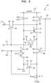
- FIG. 2 is an equivalent circuit diagram of one of the pixels PX provided in the display apparatus of FIG. 1 .
- one of the pixels PX may include a plurality of signal lines 121, 122, 123, and 171, a plurality of thin film transistors (TFTs) T1, T2, T3, 4, T5, T6, and T7 connected to the signal lines, a storage capacitor Cst, an initialization voltage line 124, a driving voltage line 172, and the OLED.
- TFTs thin film transistors
- FIG. 2 illustrates an example in which the signal lines 121, 122, 123, and 171 and the driving voltage line 172 are provided for each pixel PX, but the present disclosure is not limited thereto. In another embodiment, at least one of the signal lines 121, 122, 123, and 171 and/or the driving voltage line 172 may be shared with neighboring pixels.
- the TFTs T1, T2, T3, T4, T5, T6, and T7 may include a driving TFT T1, a switching TFT T2, a compensation TFT T3, a first initialization TFT T4, an operation control TFT T5, an emission control TFT T6, and a second initialization TFT T7.
- the signal lines 121, 122, 123, and 171 may include a scan line 121 for transmitting a scan signal Sn, a previous scan line 122 for transmitting a previous scan signal Sn-1 to the first initialization TFT T4 and the second initialization TFT T7, an emission control line 123 for transmitting an emission control signal En to the operation control TFT T5 and the emission control TFT T6, and a data line 171 for transmitting a data signal Dm, the data line 171 intersecting the scan line 121.
- the driving voltage line 172 transmits a driving voltage ELVDD and is formed substantially parallel to the data line 171, and the initialization voltage line 124 transmits an initialization voltage Vint to initialize the driving TFT T1.
- a driving gate electrode G1 of the driving TFT T1 is connected to a first storage capacitor plate Cst1 of the storage capacitor Cst.
- a driving source electrode S1 of the driving TFT T1 is connected to the driving voltage line 172 that is a lower driving voltage line, via the operation control TFT T5.
- a driving drain electrode D1 of the driving TFT T1 is electrically connected to a pixel electrode of the OLED via the emission control TFT T6. According to a switching operation of the switching TFT T2, the driving TFT T1 receives the data signal Dm and supplies a driving current I OLED to the OLED.
- a switching gate electrode G2 of the switching TFT T2 is connected to the scan line 121.
- a switching source electrode S2 of the switching TFT T2 is connected to the data line 171.
- a switching drain electrode D2 of the switching TFT T2 is connected to the driving source electrode S1 of the driving TFT T1 and to the driving voltage line 172 via the operation control TFT T5.
- the switching TFT T2 is turned on in response to the scan signal Sn received through the scan line 121 and performs the switching operation of transmitting the data signal Dm received through the data line 171 to the driving source electrode S1 of the driving TFT T1.
- a compensation gate electrode G3 of the compensation TFT T3 is connected to the scan line 121.
- a compensation source electrode S3 of the compensation TFT T3 is connected to the driving drain electrode D1 of the driving TFT T1 and is connected to the pixel electrode of the OLED via the emission control TFT T6.
- a compensation drain electrode D3 of the compensation TFT T3 is connected to the first storage capacitor plate Cst1 of the storage capacitor Cst, a first initialization drain electrode D4 of the first initialization TFT T4, and the driving gate electrode G1 of the driving TFT T1.
- the compensation TFT T3 is turned on in response to the scan signal Sn received through the scan line 121 and electrically connects the driving gate electrode G1 and the driving drain electrode D1 of the driving TFT T1, thereby having the driving TFT T1 diode-connected.
- a first initialization gate electrode G4 of the first initialization TFT T4 is connected to the previous scan line 122.
- a first initialization source electrode S4 of the first initialization TFT T4 is connected to a second initialization drain electrode D7 of the second initialization TFT T7 and the initialization voltage line 124.
- the first initialization drain electrode D4 of the first initialization TFT T4 is connected to the first storage capacitor plate Cst1 of the storage capacitor Cst, the compensation drain electrode D3 of the compensation TFT T3, and the driving gate electrode G1 of the driving TFT T1.
- the first initialization TFT T4 is turned on in response to the previous scan signal Sn-1 received through the previous scan line 122 and performs an initialization operation to initialize a voltage of the driving gate electrode G1 of the driving TFT T1 by transmitting the initialization voltage Vint to the driving gate electrode G1 of the driving TFT T1.
- An operation control gate electrode G5 of the operation control TFT T5 is connected to the emission control line 123.
- An operation control source electrode S5 of the operation control TFT T5 is connected to the driving voltage line 172.
- An operation control drain electrode D5 of the operation control TFT T5 is connected to the driving source electrode S1 of the driving TFT T1 and the switching drain electrode D2 of the switching TFT T2.
- An emission control gate electrode G6 of the emission control TFT T6 is connected to the emission control line 123.
- An emission control source electrode S6 of the emission control TFT T6 is connected to the driving drain electrode D1 of the driving TFT T1 and the compensation source electrode S3 of the compensation TFT T3.
- An emission control drain electrode D6 of the emission control TFT T6 is electrically connected to a second initialization source electrode S7 of the second initialization TFT T7 and the pixel electrode of the OLED.
- the operation control TFT T5 and the emission control TFT T6 are simultaneously turned on in response to the emission control signal En received through the emission control line 123, and thus the driving voltage ELVDD is transmitted to the OLED, and the driving current I OLED flows through the OLED.
- a second initialization gate electrode G7 of the second initialization TFT T7 is connected to the previous scan line 122.
- the second initialization source electrode S7 of the second initialization TFT T7 is connected to the emission control drain electrode D6 of the emission control TFT T6 and the pixel electrode of the OLED.
- the second initialization drain electrode D7 of the second initialization TFT T7 is connected to the first initialization source electrode S4 of the first initialization TFT T4 and the initialization voltage line 124.
- the second initialization TFT T7 is turned on in response to the previous scan signal Sn-1 received through the previous scan line 122 and initializes the pixel electrode of the OLED.
- FIG. 2 illustrates an example in which the first initialization TFT T4 and the second initialization TFT T7 are connected to the previous scan line 122
- the present disclosure is not limited thereto.
- the first initialization TFT T4 may be connected to the previous scan line 122 and driven by the previous scan signal Sn-1
- the second initialization TFT T7 may be connected to a separate signal line (e.g., a next scan line) and driven by a signal transmitted to the separate signal line.
- a second storage capacitor plate Cst2 of the storage capacitor Cst is connected to the driving voltage line 172 and an opposite electrode of the OLED is connected to a common voltage ELVSS. Accordingly, the OLED may display an image by receiving the driving current I OLED from the driving TFT T1 and emitting light.
- FIG. 2 illustrates an example in which each of the compensation TFT T3 and the first initialization TFT T4 has a dual gate electrode
- the present disclosure is not limited thereto.
- each of the compensation TFT T3 and the first initialization TFT T4 may have a single gate electrode.
- various modifications are possible such that at least one of the driving TFT T1, the switching TFT T2, the operation control TFT T5, the emission control TFT T6, and the second initialization TFT T7 may have a dual gate electrode.
- the first initialization TFT T4 is turned on in response to the previous scan signal Sn-1 and the driving TFT T1 is initialized by the initialization voltage Vint supplied through the initialization voltage line 124.
- the switching TFT T2 and the compensation TFT T3 are turned on in response to the scan signal Sn.
- the driving TFT T1 is diode-connected by the compensation TFT T3 that is turned on, and is biased in a forward direction.
- a compensated voltage Dm+Vth is applied to the driving gate electrode G1 of the driving TFT T1.
- the compensated voltage Dm+Vth is obtained by subtracting a threshold voltage Vth of the driving TFT T1 from the data signal Dm of the data line 171.
- the driving voltage ELVDD and the compensated voltage Dm+Vth are applied to both ends of the storage capacitor Cst, and electric charges corresponding to a voltage difference between both ends are stored in the storage capacitor Cst.
- the operation control TFT T5 and the emission control TFT T6 are turned on by the emission control signal En supplied through the emission control line 123.
- the driving current I OLED according to a voltage difference between a voltage of the driving gate electrode G1 of the driving TFT T1 and the driving voltage ELVDD is generated, and the driving current I OLED is supplied to the OLED through the emission control TFT T6.
- FIG. 3 is a layout schematically illustrating positions of a plurality of TFTs, a storage capacitor, and a pixel electrode of the pixel PX of FIG. 2 .
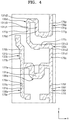
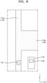
- FIGS. 4 to 9 are layouts schematically illustrating elements, such as the plurality of TFTs, the storage capacitor, and the pixel electrode shown in FIG. 3 , layer by layer.
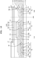
- FIG. 10 is a cross-sectional view taken along lines A-A and B-B of FIG. 3 .
- FIGS. 4 to 9 illustrates arrangements of a wiring, an electrode, a semiconductor layer, and the like located on the same layer, and an insulating layer may be interposed between layers shown in FIGS. 4 to 9 .
- a first gate insulating layer 141 (see FIG. 10 ) is interposed between a layer shown in FIG. 4 and a layer shown in FIG. 5
- a second gate insulating layer 143 (see FIG. 10 ) is interposed between a layer shown in FIG. 5 and a layer shown in FIG. 6
- a first interlayer insulating layer 150 (see FIG. 10 ) is interposed between a layer shown in FIG. 6 and a layer shown in FIG.
- FIG. 7 a second interlayer insulating layer 160 (see FIG. 10 ) is interposed between a layer shown in FIG. 7 and a layer shown in FIG. 8 .
- a planarization insulating layer 180 (see FIG. 10 ) is interposed between a layer shown in FIG. 8 and a layer shown in FIG. 9 .
- the layers shown in FIGS. 4 to 9 may be electrically connected to each other.
- the pixel PX includes the scan line 121, the previous scan line 122, the emission control line 123, and the initialization voltage line 124, to which the scan signal Sn, the previous scan signal Sn-1, the emission control signal En, and the initialization voltage Vint are respectively applied.
- the pixel PX includes the scan line 121, the previous scan line 122, the emission control line 123, and the initialization voltage line 124 extend in a second direction (x direction, hereinafter also referred to as "row direction").
- the pixel PX may include the data line 171 and the driving voltage line 172 that extend in a first direction (y direction, hereinafter also referred to as "column direction") to intersect the scan line 121, the previous scan line 122, the emission control line 123, and the initialization voltage line 124.
- the data signal Dm and the driving voltage ELVDD are respectively applied to the data line 171 and the driving voltage line 172.
- the pixel PX includes a conductive layer 178 that prevents or reduces the generation of parasitic capacitance.
- the pixel PX further includes the TFTs T1 to T7, the storage capacitor Cst, and the OLED (see FIG. 10 ) electrically connected to the TFTs T1 to T7 and the storage capacitor Cst.
- TFTs T1 to T7 the storage capacitor Cst
- OLED see FIG. 10
- semiconductor layers 130a to 130g that is, a driving semiconductor layer 130a of the driving TFT T1, a switching semiconductor layer 130b of the switching TFT T2, a compensation semiconductor layer 130c of the compensation TFT T3, a first initialization semiconductor layer 130d of the first initialization TFT T4, an operation control semiconductor layer 130e of the operation control TFT T5, an emission control semiconductor layer 130f of the emission control TFT T6, and a second initialization semiconductor layer 130g of the second initialization TFT T7, are arranged in the same layer.
- the semiconductor layers 130a to 130g are arranged on a buffer layer 111 located on the substrate 110.
- the substrate 110 may include a glass material, a metal material, or a plastic material such as polyethylene terephthalate (PET), polyethylenenaphthalate (PEN), or polyimide.
- the buffer layer 111 may include an oxide film such as silicon oxide (SiOx) and/or a nitride film such as silicon nitride (SiNx).
- the driving semiconductor layer 130a of the driving TFT T1, the switching semiconductor layer 130b of the switching TFT T2, the compensation semiconductor layer 130c of the compensation TFT T3, the first initialization semiconductor layer 130d of the first initialization TFT T4, the operation control semiconductor layer 130e of the operation control TFT T5, the emission control semiconductor layer 130f of the emission control TFT T6, and the second initialization semiconductor layer 130g of the second initialization TFT T7 may be connected to one another and curved in various shapes.
- the semiconductor layers 130a to 130g may include polycrystalline silicon.
- the semiconductor layers 130a to 130g may include amorphous silicon or an oxide semiconductor layer such as a G-I-Z-O layer [(In 2 O 3 )a(Ga 2 O 3 )b(ZnO)c layer] (where a, b, and c are real numbers satisfying the conditions of a ⁇ 0, b ⁇ 0, and c > 0, respectively).
- a, b, and c are real numbers satisfying the conditions of a ⁇ 0, b ⁇ 0, and c > 0, respectively.
- the semiconductor layers 130a to 130g may include a channel region, and a source region and a drain region provided at both sides of the channel region.
- the source region and the drain region may be doped with impurities, and the impurities may include N-type impurities or P-type impurities.
- the source region and the drain region are electrically connected to a source electrode and a drain electrode, respectively, and thus correspond to the source electrode and the drain electrode, respectively.
- the source electrode and the drain electrode are respectively referred to as the source region and the drain region.
- the driving semiconductor layer 130a includes a driving channel region 131a, and a driving source region 176a and a driving drain region 177a provided at both sides of the driving channel region 131a.
- the driving channel region 131a may be formed longer than the other channel regions 131b to 131g.
- the driving channel region 131a has a multiply bent shape such as "S" or " ⁇ "
- a long channel length may be attained in a narrow space. Since the driving channel region 131a is formed long, a driving range of a gate voltage applied to a first electrode layer 125a (i.e., the driving gate electrode G1 of the driving TFT T1) increases, and thus gradation of light emitted from the OLED may be more accurately controlled, thereby improving display quality.
- the switching semiconductor layer 130b includes a switching channel region 131b, and a switching source region 176b and a switching drain region 177b provided at both sides of the switching channel region 131b.
- the switching drain region 177b is connected to the driving source region 176a.
- the compensation semiconductor layer 130c includes compensation channel regions 131c1 and 131c3, and a compensation source region 176c and a compensation drain region 177c provided at both sides of the compensation channel regions 131c1 and 131c3.
- the compensation TFT T3 formed in the compensation semiconductor layer 130c is a dual TFT and includes two compensation channel regions 131c1 and 131c3.
- a region 131c2 between the compensation channel regions 131c1 and 131c3 is an impurity-doped region, and locally corresponds to a source region of one transistor of the dual TFT and a drain region of the other transistor of the dual TFT.
- the first initialization semiconductor layer 130d includes first initialization channel regions 131d1 and 131d3, and a first initialization source region 176d and a first initialization drain region 177d provided at both sides of the first initialization channel regions 131d1 and 131d3.
- the first initialization TFT T4 formed in the first initialization semiconductor layer 130d is a dual TFT and includes two first initialization channel regions 131d1 and 131d3.
- a region 131d2 between the first initialization channel regions 131d1 and 131d3 is an impurity-doped region, and locally corresponds to a source region of one transistor of the dual TFT and a drain region of the other transistor of the dual TFT.
- the operation control semiconductor layer 130e includes an operation control channel region 131e, and an operation control source region 176e and an operation control drain region 177e provided at both sides of the operation control channel region 131e.
- the operation control drain region 177e may be connected to the driving source region 176a.
- the emission control semiconductor layer 130f includes an emission control channel region 131f, and an emission control source region 176f and an emission control drain region 177f provided at both sides of the emission control channel region 131f.
- the emission control source region 176f may be connected to the driving drain region 177a.
- the second initialization semiconductor layer 130g includes a second initialization channel region 131g, and a second initialization source region 176g and a second initialization drain region 177g provided at both sides of the second initialization channel region 131g.
- the first gate insulating layer 141 is located on the semiconductor layers 130a to 130g.
- the first gate insulating layer 141 may include an inorganic material including an oxide or a nitride.
- the first gate insulating layer 141 may include silicon oxide (SiO 2 ), silicon nitride (SiN x ), silicon oxynitride (SiON), aluminum oxide (Al 2 O 3 ), titanium oxide (TiO 2 ), tantalum oxide (Ta 2 O 5 ), hafnium oxide (HfO 2 ), zinc oxide (ZnO 2 ), or the like.
- the scan line 121, the previous scan line 122, the emission control line 123, and the first electrode layer 125a are located on the first gate insulating layer 141.
- the scan line 121, the previous scan line 122, the emission control line 123, and the first electrode layer 125a may include the same material.
- the scan line 121, the previous scan line 122, the emission control line 123, and the first electrode layer 125a may include molybdenum (Mo), aluminum (Al), copper (Cu), titanium (Ti), or the like, and may include a single layer or multiple layers.
- Parts and protruding portions of the scan line 121, the previous scan line 122, the emission control line 123, and the first electrode layer 125a respectively correspond to the gate electrodes of the TFTs T1 to T7. That is, portions of the scan line 121, the previous scan line 122, the emission control line 123, and the first electrode layer 125a that overlap the semiconductor layers 130a to 130g are defined as gate electrodes.
- a region of the scan line 121 that overlaps the switching channel region 131b corresponds to a switching gate electrode 125b
- regions of the scan line 121 that overlap the compensation channel regions 131c1 and 131c3 correspond to compensation gate electrodes 125c1 and 125c2.
- Regions of the previous scan line 122 that overlap the first initialization channel regions 131d1 and 131d3 correspond to first initialization gate electrodes 125d1 and 125d2
- a region of the previous scan line 122 that overlaps the second initialization channel region 131g corresponds to a second initialization gate electrode 125g.
- a region of the emission control line 123 that overlaps the operation control channel region 131e corresponds to an operation control gate electrode 125e
- a region of the emission control line 123 that overlaps the emission control channel region 131f corresponds to an emission control gate electrode 125f.
- the compensation gate electrodes 125c1 and 125c2 correspond to a dual gate electrode including a first compensation gate electrode 125c1 and a second compensation gate electrode 125c2 and may prevent or reduce the occurrence of a leakage current.
- a portion of the first electrode layer 125a that overlaps the driving channel region 131a corresponds to the driving gate electrode G1 of the driving TFT T1.
- the first electrode layer 125a is used as the driving gate electrode G1 of the driving TFT T1 and the first storage capacitor plate Cst1 of the storage capacitor Cst.
- the driving gate electrode G1 of the driving TFT T1 and the first storage capacitor plate Cst1 of the storage capacitor Cst are integrally formed.
- the second gate insulating layer 143 is located on the scan line 121, the previous scan line 122, the emission control line 123, and the first electrode layer 125a.
- the second gate insulating layer 143 may include an inorganic material including an oxide or a nitride.
- the second gate insulating layer 143 may include silicon oxide (SiO 2 ), silicon nitride (SiN x ), silicon oxynitride (SiON), aluminum oxide (Al 2 O 3 ), titanium oxide (TiO 2 ), tantalum oxide (Ta 2 O 5 ), hafnium oxide (HfO 2 ), zinc oxide (ZnO 2 ), or the like.
- the initialization voltage line 124, a plate 126, and a second electrode layer 127 are located on the second gate insulating layer 143.
- the initialization voltage line 124, the plate 126, and the second electrode layer 127 may include the same material.
- the initialization voltage line 124, the plate 126, and the second electrode layer 127 may include molybdenum (Mo), aluminum (Al), copper (Cu), titanium (Ti), or the like, and may include a single layer or multiple layers.
- Portions of the initialization voltage line 124 that overlap the first and second initialization channel regions 131d1, 131d3, and 131g correspond to the first and second initialization gate electrodes 125d1, 125d2, and 125g, respectively.
- the plate 126 is electrically connected to the driving voltage line 172 through a contact hole 159, as shown in FIG. 3 , and may cover a portion of the switching source region 176b. In some embodiments, the plate 126 may cover the second initialization drain region 177g and/or the first initialization source region 176d.
- the plate 126 that is electrically connected to the driving voltage line 172 to which a constant voltage (i.e., the driving voltage ELVDD) is applied may reduce or block influence on the switching TFT T2 and the first and second initialization TFTs T4 and T7 by other peripheral electrical signals.
- the second electrode layer 127 overlaps the first electrode layer 125a with the second gate insulating layer 143 between the second electrode layer 127 and the first electrode layer 125a.
- the second electrode layer 127 corresponds to the second storage capacitor plate Cst2 of the storage capacitor Cst.
- the second electrode layer 127 includes an opening 27 exposing a portion of the first electrode layer 125a.
- One end of a node connection line 174 is electrically connected to the first electrode layer 125a through the opening 27.
- the first interlayer insulating layer 150 is located on the initialization voltage line 124, the plate 126, and the second electrode layer 127.
- the first interlayer insulating layer 150 may include silicon oxide (SiO 2 ), silicon nitride (SiN x ), silicon oxynitride (SiON), aluminum oxide (Al 2 O 3 ), titanium oxide (TiO 2 ), tantalum oxide (Ta 2 O 5 ), hafnium oxide (HfO 2 ), zinc oxide (ZnO 2 ), or the like.
- the data line 171, the driving voltage line 172, an initialization connection line 173, the node connection line 174, and an intermediate connection layer 175 are located on the first interlayer insulating layer 150.
- the data line 171, the driving voltage line 172, the initialization connection line 173, the node connection line 174, and the intermediate connection layer 175 may include the same material.
- the data line 171, the driving voltage line 172, the initialization connection line 173, the node connection line 174, and the intermediate connection layer 175 may include a conductive material including molybdenum (Mo), aluminum (Al), copper (Cu), titanium (Ti), or the like, and may include a single layer or multiple layers including the conductive material.
- the data line 171, the driving voltage line 172, the initialization connection line 173, the node connection line 174, and the intermediate connection layer 175 may have a multilayered structure of Ti/Al/Ti.
- the data line 171 extends in the column direction (y direction) and is connected to the switching source region 176b of the switching TFT T2 through a contact hole 154 defined in the first interlayer insulating layer 150.
- the driving voltage line 172 extends in the column direction (y direction) and is connected to the operation control source region 176e of the operation control TFT T5 and the second electrode layer 127 respectively through contact holes 155 and 158 defined in the first interlayer insulating layer 150.
- the driving voltage line 172 may be connected to the plate 126 through the contact hole 159 defined in the first interlayer insulating layer 150.
- the initialization connection line 173 connects the initialization source region 176d of the first initialization TFT T4 to the initialization voltage line 124 through contact holes 151 and 152 defined in the first interlayer insulating layer 150.
- the node connection line 174 connects the first electrode layer 125a to the compensation drain region 177c of the compensation TFT T3 through contact holes 156 and 157.
- the first electrode layer 125a having an island shape may be electrically connected to the compensation TFT T3 via the node connection line 174.
- the intermediate connection layer 175 is connected to the emission control TFT T6 through a contact hole 153.
- the intermediate connection layer 175 may be connected to the emission control drain region 177f of the emission control TFT T6.
- the second interlayer insulating layer 160 is located on the data line 171, the driving voltage line 172, the initialization connection line 173, the node connection line 174, and the intermediate connection layer 175.
- the second interlayer insulating layer 160 may include an inorganic insulating material such as silicon oxide (SiO 2 ), silicon nitride (SiN x ), silicon oxynitride (SiON), aluminum oxide (Al 2 O 3 ), titanium oxide (TiO 2 ), tantalum oxide (Ta 2 O 5 ), hafnium oxide (HfO 2 ), or zinc oxide (ZnO 2 ).
- the second interlayer insulating layer 160 may include a film including the above-described inorganic insulating material and a film including an organic insulating material.
- the conductive layer 178 and an auxiliary connection layer 179 are located on the second interlayer insulating layer 160.
- the conductive layer 178 and the auxiliary connection layer 179 may include the same material.
- the conductive layer 178 and the auxiliary connection layer 179 may include a conductive material including molybdenum (Mo), aluminum (Al), copper (Cu), titanium (Ti), or the like, and may include a single layer or multiple layers including the conductive material.
- the conductive layer 178 and the auxiliary connection layer 179 may have a multilayered structure of Ti/AI/Ti.
- the conductive layer 178 includes a wiring portion 178a that extends in the column direction (y direction) and an extending portion 178b that extends in the row direction (x direction) from the wiring portion 178a.
- the extending portion 178b covers the first electrode layer 125a and the compensation TFT T3 while overlapping at least a portion of the first electrode layer 125a and the compensation TFT T3.
- the extending portion 178b may overlap a portion of the first electrode layer 125a.
- the extending portion 178b may overlap and cover the compensation channel region 131c1 of the compensation semiconductor layer 130c, at least a portion of the compensation gate electrode 125c1, and the compensation source region 176c.
- the compensation channel region 131c3 and the compensation drain region 177c that is connected to the first initialization TFT T4 may not overlap the conductive layer 178.
- the conductive layer 178 may be connected to a wiring to which a constant voltage is applied.
- the conductive layer 178 may be electrically connected to the driving voltage line 172 under the conductive layer 178 through a contact hole 161 defined in the second interlayer insulating layer 160.
- the conductive layer 178 may correspond to an upper driving voltage line
- the driving voltage line 172 may correspond to a lower driving voltage line.
- a display apparatus that provides a high-quality image would need to prevent a voltage drop or the like from occurring in the driving voltage line 172.
- the driving voltage line 172 is located in the same layer as the data line 171, the initialization connection line 173, the node connection line 174, the intermediate connection layer 175, and the like, and thus the extent to which the area of the driving voltage line 172 may be expanded in this layer is spatially limited.
- the conductive layer 178 that is an upper driving voltage line, and the driving voltage line 172 that is a lower driving voltage line are electrically connected to each other, an issue of the voltage drop may be resolved.
- the conductive layer 178 corresponds to a wiring to which the driving voltage ELVDD is applied.
- ELVDD driving voltage
- a color abnormality defect according to a viewing angle may occur due to the asymmetry of the wiring portion 178a located under the light-emitting region EM.
- the light-emitting region EM is asymmetrically divided by the wiring portion 178a in a plane view, and this asymmetry may result in a color abnormality defect according to a viewing angle.
- the wiring portion 178a is provided not to overlap the light-emitting region EM. Therefore, the present display apparatus may not exhibit the color abnormality defect of the light-emitting region EM that may occur due to the asymmetry of the wiring portion 178a that passes under the light-emitting region EM.
- the extending portion 178b of the conductive layer 178 may be interposed between a pixel electrode 210 and the first electrode layer 125a overlapping the pixel electrode 210 and the first electrode layer 125a, and thus prevents or reduces parasitic capacitance Cga between the pixel electrode 210 and the gate electrode G1 of the driving TFT T1.
- parasitic capacitance Cga between the pixel electrode 210 and the node connection line 174 corresponds to the parasitic capacitance Cga between the pixel electrode 210 and the gate electrode G1 of the driving TFT T1.
- the extending portion 178b overlaps the node connection line 174 while overlapping the pixel electrode 210 and thus may prevent or reduce the parasitic capacitance Cga.
- the driving current I OLED may not be constant in a saturation region and may unintentionally increase, due to the parasitic capacitance Cga.
- the driving current I OLED may unintentionally increase in the saturation region in the absence of the extending portion 178b, causing a current deviation. In this case, the OLED may emit light at a luminance that is different from that intended originally.
- the parasitic capacitance Cga is prevented or reduced by the extending portion 178b, an increase in the drive current I OLED in the saturation region is suppressed. Accordingly, the OLED may be prevented from emitting light at a luminance that is different from that intended originally, and color deviation may be reduced, thereby preventing deterioration of the quality of images provided by the display apparatus.
- the auxiliary connection layer 179 is connected to the intermediate connection layer 175 through a contact hole 163, and a planarization insulating layer 180 is located on the conductive layer 178 and the auxiliary connection layer 179.
- the planarization insulating layer 180 may include an organic material such as acryl, benzocyclobutene (BCB), polyimide, or hexamethyldisiloxane (HMDSO).
- the pixel electrode 210 is located on the planarization insulating layer 180.
- the pixel electrode 210 is connected to the auxiliary connection layer 179 through a contact hole 185 defined in the planarization insulating layer 180.
- the pixel electrode 210 is connected to the emission control drain region 177f of the emission control TFT T6 by the auxiliary connection layer 179 and the intermediate connection layer 175.
- the pixel electrode 210 may be a reflective electrode.
- the pixel electrode 210 may include a reflective film including Ag, Mg, Al, Pt, Pd, Au, Ni, Nd, Ir, Cr or a compound thereof and a transparent or translucent electrode layer formed on the reflective film.
- the transparent or translucent electrode layer may include at least one selected from the group consisting of indium tin oxide (ITO), indium zinc oxide (IZO), zinc oxide (ZnO), indium oxide (In 2 O 3 ), indium gallium oxide (IGO), and aluminum zinc oxide (AZO).
- a pixel-defining layer 190 that exposes the pixel electrode 210 is located on the pixel electrode 210.
- the pixel-defining layer 190 may include at least one organic insulating material selected from the group consisting of polyimide, polyamide, acrylic resin, benzocyclobutene, and phenol resin.
- the pixel-defining layer 190 covers the edge of the pixel electrode 210 and has an opening OP for exposing at least a portion of the upper surface of the pixel electrode 210.
- the light-emitting region EM is defined by the opening OP of the pixel-defining layer 190.
- An emission layer 220 is located on the pixel electrode 210 exposed by the opening OP of the pixel-defining layer 190.
- the emission layer 220 may include an organic material including a fluorescent or phosphorescent material that emits red, green, blue, or white light.
- the emission layer 220 may include a low molecular organic material or a polymer organic material.
- a functional layer such as a hole transport layer (HTL), a hole injection layer (HIL), an electron transport layer (ETL), or an electron injection layer (EIL) may be selectively arranged.
- HTL hole transport layer
- HIL hole injection layer
- ETL electron transport layer
- EIL electron injection layer
- An opposite electrode 230 may be a light-transmitting electrode.
- the opposite electrode 230 may be a transparent or translucent electrode and may include a metal thin film having a low work function and including Li, Ca, LiF/Ca, LiF/AI, Al, Ag, Mg, or a compound thereof.
- a transparent conductive oxide (TCO) film such as ITO, IZO, ZnO, or In 2 O 3 may be further located on the metal thin film.
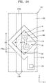
- FIG. 11 is a plan view illustrating only some of the components shown in FIGS. 7 to 10 including the node connection line 174, the conductive layer 178, the pixel electrode 210, and the pixel-defining layer 190.
- the pixel-defining layer 190 defines the light-emitting region EM via the opening OP that exposes the upper surface of the pixel electrode 210.
- the conductive layer 178 is located under the pixel electrode 210.
- the conductive layer 178 has the wiring portion 178a that extends in the column direction (y direction) and the extending portion 178b that extends from the wiring portion 178a in the row direction (x direction) intersecting the column direction (y direction).
- the wiring portion 178a is located not to overlap the light-emitting region EM.
- the light-emitting region EM may be asymmetrically divided by the wiring portion 178a in a plane view, and this asymmetry may result in a color abnormality defect according to a viewing angle. Since the conductive layer 178 is located at the top among the conductive layers located under the pixel electrode 210 as being closest to the pixel electrode 210, the conductive layer 178 has a greater effect on the light emission uniformity of the light-emitting region EM than the other conductive layers.
- the wiring portion 178a is arranged such that it avoids and does not overlap the light-emitting region EM, thereby preventing a color abnormality defect.
- the extending portion 178b is located under the pixel electrode 210 and above the node connection line 174 and overlaps the pixel electrode 210 and the node connection line 174.
- the contact hole 156 at one side of the node connection line 174 is connected to the first electrode layer 125a and the contact hole 157 at the other side of the node connection line 174 is connected to the compensation TFT T3. Therefore, the first electrode layer 125a may be electrically connected to the compensation TFT T3 by the node connection line 174.
- a parasitic capacitance Cga may be generated between the pixel electrode 210 and the gate electrode G1 of the driving TFT T1, and a color deviation defect may occur in the light-emitting region EM.
- the parasitic capacitance Cga between the pixel electrode 210 and the node connection line 174 may correspond to the parasitic capacitance Cga between the pixel electrode 210 and the gate electrode G1 of the driving TFT T1.
- the node connection line 174 overlaps the light-emitting region EM, and the parasitic capacitance Cga between the pixel electrode 210 and the node connection line 174 may cause a color deviation defect in the light-emitting region EM.
- the present display apparatus can prevent or reduce the generation of the parasitic capacitance Cga.
- the extending portion 178b may extend in the row direction (x direction) and pass through the light-emitting region EM.
- the light-emitting region EM may be divided into an overlapping region OA that overlaps the extending portion 178b, a first region 1A located at one side of the overlapping region OA, and a second region 2A located at the other side of the overlapping region OA.
- the size of the first region 1A may be equal to that of the second region 2A, and the first region 1A and the second region 2A may be symmetrical to each other with respect to the overlapping region OA.
- the extending portion 178b is located under the light-emitting region EM to block or reduce the parasitic capacitance Cga between the pixel electrode 210 and the node connection line 174.
- the extending portion 178b passes the light-emitting region EM while asymmetrically dividing the light-emitting region EM, this asymmetry may cause a color abnormality defect according to a viewing angle of the light-emitting region EM. Therefore, the extending portion 178b is arranged to pass over the geometrical center of the light-emitting region EM in a plane view when the extending portion 178b passes under the light-emitting region EM.
- the extending portion 178b is arranged to divide the light-emitting region EM symmetrically in a plane view, so that a color abnormality defect according to the viewing angle of the light-emitting region EM that may be otherwise caused by the asymmetry, can be resolved.
- FIGS. 12 and 13 illustrate embodiments modified from the embodiment of FIG. 11 .
- the embodiment of FIG. 12 differs from the embodiment of FIG. 11 in the structure of the extending portion 178b. All other components except the extending portion 178b are substantially the same as those described with respect to the embodiment of FIG. 11 .
- the extending portion 178b extends in the row direction (x direction) from the wiring portion 178a and entirely overlaps the light-emitting region EM. That is, the extending portion 178b overlaps the entire surface of the light-emitting region EM, so that the light-emitting region EM may emit light of the same luminance from the entire surface of the light-emitting region EM regardless of the position of the node connection line 174 that may cause the parasitic capacitance Cga.
- FIG. 13 illustrates a first pixel PX1, a second pixel PX2, and a third pixel PX3.
- Each of the first to third pixels PX1, PX2, and PX3 is similar to the embodiment of FIG. 10 , and FIG. 13 shows a structure in which the extending portion 178b is consecutively arranged in the first to third pixels PX1, PX2, and PX3.
- the first pixel PX1 includes a first pixel electrode 211 and a first conductive layer 178-1
- the second pixel PX2 includes a second pixel electrode 212 and a second conductive layer 178-2
- the third pixel PX3 includes a third pixel electrode 213 and a third conductive layer 178-3.
- the pixel-defining layer 190 has a first opening OP1, a second opening OP2, and a third opening OP3 respectively exposing at least a portion of the upper surfaces of the first to third pixel electrodes 211, 212, and 213, and first to third light-emitting regions EM1, EM2, and EM3 in the first to third pixels PX1, PX2, and PX3 are defined by the first to third openings OP1, OP2, and OP3.
- the first light-emitting region EM1 of the first pixel PX1 emits light of a red color wavelength
- the second light-emitting region EM2 of the second pixel PX2 emits light of a green color wavelength
- the third light-emitting region EM3 of the third pixel PX3 emits light of a green color wavelength
- the first conductive layer 178-1 of the first pixel PX1 includes a first wiring portion 178a-1 and a first extending portion 178b-1
- the second conductive layer 178-2 of the second pixel PX2 includes a second wiring portion 178a-2 and a second extending portion 178b-2
- the third conductive layer 178-3 of the third pixel PX3 includes a third wiring portion 178a-3 and a third extending portion 178b-3.
- the first to third wiring portions 178a-1, 178a-2, and 178a-3 extend in the column direction (y direction) in parallel with each other
- the first to third extending portions 178b-1, 178b-2, and 178b-3 extend in the row direction (x direction).
- the first extending portion 178b-1 covers a first node connection line 174-1 under the first pixel electrode 211 and extends in the row direction (x direction) from a portion of the first wiring portion 178a-1 to symmetrically divide the first light-emitting region EM1 in a plane view.
- the second extending portion 178b-2 covers a second node connection line 174-2 under the second pixel electrode 212 and extends in the row direction (x direction) from a portion of the second wiring portion 178a-2 to symmetrically divide the second light-emitting region EM2 in the plane view.
- the third extending portion 178b-3 covers a third node connection line 174-3 under the third pixel electrode 213 and extends in the row direction (x direction) from a portion of the third wiring portion 178a-3 to symmetrically divide the third light-emitting region EM3 in the plane view.
- the first extending portion 178b-1 extends to the second pixel PX2 to connect the first wiring portion 178a-1 to the second wiring portion 178a-2.
- the second extending portion 178b-2 extends to the third pixel PX3 to connect the second wiring portion 178a-2 to the third wiring portion 178a-3.
- the third extending portion 178b-3 also connects the third wiring portion 178a-3 to a wiring portion (not shown, e.g., the first wiring portion) of a pixel (not shown) that is adjacent to the third pixel PX3.
- the first to third extending portions 178b-1, 178b-2, and 178b-3 may be consecutively arranged and integrally formed.
- the first to third wiring portions 178a-1, 178a-2, and 178a-3 are electrically and physically connected to each other by the first to third extending portions 178b-1, 178b-2, and 178b-3
- the first to third conductive layers 178-1, 178-2, and 178-3 may have a mesh structure.
- FIGS. 11 to 13 illustrate examples where the light-emitting region EM is rectangular, the light-emitting region EM may be provided in various shapes in a plane view.
- the light-emitting region EM may have various shapes such as a polygon, an ellipse, and a polygon with rounded corners.
- FIGS. 1 to 13 illustrate examples where a plurality of pixels are provided in the form of stripes
- the plurality of pixels may be provided in a square form or a PenTile form, and the above descriptions may be equally applicable to pixels of the square form or the PenTile form.
- FIGS. 14 to 16 illustrate examples where a light-emitting region EM is formed in a diamond shape.
- FIGS. 14 to 16 only a node connection line 174, a conductive layer 178, a pixel electrode 210, and a pixel-defining layer 190 are shown, and other configurations are substantially the same as those described with respect to the above-described embodiments.
- a pixel PX includes the node connection line 174, the conductive layer 178 located on the node connection line 174, the pixel electrode 210 located on the conductive layer 178, and the pixel-defining layer 190 located on the pixel electrode 210.
- the pixel-defining layer 190 defines the light-emitting region EM through an opening OP that exposes at least a portion of an upper surface of the pixel electrode 210.
- the light-emitting region EM may be formed in a diamond shape.
- the width in the row direction (x direction) may be greater than that in a pixel having a rectangular shaped-light-emitting region formed in the column direction (y direction), and thus, it may not be easy to design the wiring portion 178a that can avoid the light-emitting region EM.
- the wiring portion 178a overlaps the light-emitting region (EM), and the extending portion 178b is provided by an overlapping width. That is, the wiring portion 178a may overlap the light-emitting region EM with a minimum first width w1 to a maximum second width w2 (in the column direction), and the extending portion 178b may have a width w3 that is equal to the maximum second width w2 of the wiring portion 178a.
- the extending portion 178b passes over the geometrical center O of the light-emitting region EM in a plane view.
- the geometrical center O of the light-emitting region EM may be defined as a point where lines connecting edges meet when the light-emitting region EM is a polygon in a plane view.
- the light-emitting region EM may have an overlapping region OA that overlaps the extending portion 178b, and a first region 1A at one side of the overlapping region OA and a second region 1B at the other side of the overlapping region OA may be symmetrical to each other.
- the node connection line 174 is shown as being entirely covered by the extending portion 178b. However, when a region where the node connection line 174 and the light-emitting region EM overlap each other is not completely covered by the extending portion 178b, the width of the extending portion 178b may increase such that the region where the node connection line 174 and the light-emitting region EM overlap each other is completely covered by the extending portion 178b.
- a wiring portion 178a is arranged to avoid the light-emitting region EM in a plane view. Therefore, a visibility color deviation problem of the light-emitting region EM may be resolved by the wiring portion 178a.
- a problem of color deviation of the light-emitting region EM may occur due to the parasitic capacitance Cga that may be generated between the node connection line 174 and the pixel electrode 210.
- the extending portion 178b may pass over the geometrical center O of the light-emitting region EM and cover a region where a portion of the node connection line 174 overlaps the light-emitting region EM.
- the extending portion 178b that passes under the light-emitting region EM is arranged to divide the light-emitting region EM symmetrically in a plane view.
- the extending portion 178b may block the parasitic capacitance Cga that may be generated between the node connection line 174 and the pixel electrode 210, thereby preventing a color deviation defect of the light-emitting region EM.
- FIG. 16 is substantially the same as FIG. 15 , except that the extending portion 178b is arranged to entirely overlap the light-emitting region EM. As the extending portion 178b overlaps the entire surface of the light-emitting region EM, the parasitic capacitance Cga that may be generated between the node connection line 174 and the pixel electrode 210 may be completely blocked.
- FIG. 16 illustrates an example in which the area of the extending portion 178b is greater than that of the light-emitting region EM, the present disclosure is not limited thereto.
- the size of the extending portion 178b may be equal to that of the light-emitting region EM as long as the extending portion 178b overlaps the entire surface of the light-emitting region EM.
- One side 178b1 of the extending portion 178b may be connected to a wiring portion 178a and the other side 178b2 may extend to the periphery of the pixel PX.
- the other side 178b2 of the extending portion 178b may be connected to a wiring portion of another pixel that is adjacent to the pixel PX.
- FIGS. 17 to 21 illustrate examples where a plurality of pixels are provided in a PenTile type.
- FIGS. 17 to 20 only node connection lines 174-1 and 174-2, conductive layers 178-1 and 178-2, pixel electrodes 211' and 212', and a pixel-defining layer 190 are shown, and other configurations are substantially the same as those described with respect to the above-described embodiments.
- FIGS. 17 to 19 illustrate a first pixel PX1' and a second pixel PX2' that are adjacent to each other.
- FIG. 20 illustrates a first pixel PX1', a second pixel PX2', a third pixel PX3', and a fourth pixel PX4'
- FIG. 21 illustrates a structure in which the structure of FIG. 20 including the first to fourth pixels PX1', PX2', PX3', and PX4' is repeated.
- the first to fourth pixels PX1', PX2', PX3', and PX4' may be pixels that emit light of different colors.
- the areas of the second and fourth light-emitting regions EM2 and EM4 in the second and fourth pixels PX2' and PX4' are smaller than the areas of the first and third light-emitting regions EM1 and EM3 in the first and third pixels PX1' and PX3'.
- the present disclosure is not limited to shapes or areas of the first to fourth light-emitting regions EM1 to EM4 shown in FIGS. 17 to 20 , and the shapes or the areas of the first to fourth light-emitting regions EM1 to EM4 may be freely modified without deviating from the scope of the present disclosure.
- the first pixel PX1' includes a first node connection line 174-1, a first conductive layer 178-1, a first pixel electrode 211', and a pixel-defining layer 190 having a first opening OP1 that are sequentially stacked.
- the pixel-defining layer 190 defines the first light-emitting region EM1 through the first opening OP1 that exposes at least a portion of an upper surface of the first pixel electrode 211'.
- the first light-emitting region EM1 of the first pixel PX1' may be formed in a diamond shape.
- the first conductive layer 178-1 includes a first wiring portion 178a-1 and a first extending portion 178b-1 that may be integrally formed.
- the first extending portion 178b-1 may be a portion that extends from the first wiring portion 178a-1.
- the second pixel PX2' includes a second node connection line 174-2, a second conductive layer 178-2 including a second wiring portion 178a-2 and a second extending portion 178b-2, a second pixel electrode 212', and a pixel-defining layer 190 having a second opening OP2 that are sequentially stacked.
- the pixel-defining layer 190 defines the second light-emitting region EM2 through the second opening OP2 that exposes at least a portion of an upper surface of the second pixel electrode 212'.
- the second light-emitting region EM2 of the second pixel PX2' may be formed in an obliquely arranged rectangular shape.
- the second conductive layer 178-2 includes the second wiring portion 178a-2 and the second extending portion 178b-2 that may be integrally formed.
- the second extending portion 178b-2 may be a portion that extends from the second wiring portion 178a-2.
- the first wiring portion 178a-1 and the second wiring portion 178a-2 extend in the column direction (y direction) in parallel with each other.
- the first extending portion 178b-1 may extend from the first wiring portion 178a-1 in the row direction (x direction) to connect the first wiring portion 178a-1 to the second wiring portion 178a-2.
- the first wiring portion 178a-1 and the second wiring portion 178a-2 may be electrically connected to each other by the first extending portion 178b-1.
- the second extending portion 178b-2 may extend from the second wiring portion 178a-2 in the row direction (x direction) to connect the second wiring portion 178a-2 to a third wiring portion (not shown) of an adjacent pixel (not shown).
- the first extending portion 178b-1 covers a region where the first node connection line 174-1 overlaps the first light-emitting region EM1, and thus blocks parasitic capacitance Cga that may be generated between the first node connection line 174-1 and the first pixel electrode 211'.
- the first extending portion 178b-1 may extend in the row direction (x direction) while symmetrically dividing the first light-emitting region EM1 in a plane view.
- the first extending portion 178b-1 overlaps the first light-emitting region EM1 to block the parasitic capacitance Cga. However, if the first extending portion 178b-1 extends while asymmetrically dividing the first light-emitting region EM1, there may arise a problem of visibility color deviation in the first light-emitting region EM1 by the first extending portion 178b-1. Thus, the first extending portion 178b-1 overlaps the first light-emitting region EM1 while symmetrically dividing the first light-emitting region EM1 in a plane view, thereby blocking the parasitic capacitance Cga and making light emission luminance by the first pixel PX1' to be uniform.
- the first wiring portion 178a-1 and the second wiring portion 178a-2 may be electrically connected to each other so that a conductive layer has a mesh structure as a whole.
- the second pixel electrode 212' and the second node connection line 174-2 do not overlap each other and thus the parasitic capacitance Cga may not be generated.
- the second extending portion 178b-2 overlaps the second node connection line 174-2 without overlapping the second pixel electrode 212'.
- the second extending portion 178b-2 may serve to form a mesh structure by electrically connecting the second wiring portion 178a-2 to a third wiring portion (not shown) of an adjacent pixel (not shown).
- FIG. 18 illustrates a structure in which the second node connection line 174-2 and the second pixel electrode 212' overlap each other.
- the second extending portion 178b-2 may cover a region where the second node connection line 174-2 overlaps the second pixel electrode 212', similar to the first extending portion 178b-1. That is, in various embodiments, the second extending portion 178b-2 may be arranged to deviate from an extending direction of the first extending portion 178b-1.
- the first extending portion 178b-1 entirely overlaps the first light-emitting region EM1.
- the size of the first extending portion 178b-1 is greater than that of the first light-emitting region EM1 and smaller than that of the first pixel electrode 211', but the present disclosure is not limited thereto.
- the first extending portion 178b-1 entirely overlaps the first light-emitting region EM1 and connects the first wiring portion 178a-1 to the second wiring portion 178a-2.
- One side 178b-11 of the first extending portion 178b-1 is connected to the first wiring portion 178a-1 and the other side 178b-12 is connected to the second wiring portion 178a-2.
- the first wiring portion 178a-1 and the second wiring portion 178a-2 may be electrically connected to each other by the first extending portion 178b-1.
- the second extending portion 178b-2 entirely overlaps the second light-emitting region EM2.
- One side 178b-21 of the second extending portion 178b-2 is connected to the second wiring portion 178a-2 and the other side 178b-22 is connected to a third wiring portion (not shown) of an adjacent pixel (not shown).
- the second wiring portion 178a-2 and the third wiring portion (not shown) may be electrically connected to each other by the second extending portion 178b-2.
- the first extending portion 178b-1 and the second extending portion 178b-1 overlap the first light-emitting region EM1 and the second light-emitting region EM2, respectively, therefore parasitic capacitance Cga that may be generated under the first and second light-emitting regions EM1 and EM2 may be blocked, and a color deviation problem may be resolved.
- FIG. 20 illustrates a first pixel PX1', a second pixel PX2', a third pixel PX3', and a fourth pixel PX4' that are arranged adjacent to each other in the row direction (x direction).
- Each of the first to fourth pixels PX1', PX2', PX3', and PX4' may be a pixel that emits light of different colors.
- the first to fourth pixels PX1', PX2', PX3', and PX4' may emit one of red light, green light, and blue light.
- the first light-emitting region EM1 may emit light of a red (R) wavelength
- the second light-emitting region EM2 may emit light of a green (G) wavelength
- the third light-emitting region EM3 may emit light of a blue (B) wavelength
- the fourth light-emitting region EM4 may emit light of a green (G) wavelength.
- the first to fourth wiring portions 178a-1 to 178a-4 may extend in the column direction (y direction) in parallel with each other, and the first to fourth extending portions 178b-1 to 178b-4 may extend in the row direction (x direction).
- the first to fourth extending portions 178b-1 to 178b-4 may sequentially connect the first to fourth wiring portions 178a-1 to 178a-4, and thus, the first to fourth conductive layers 178-1 178-4 may be integrally formed.
- the first and third extending portions 178b-1 and 178b-3 may extend to overlap the first and third light-emitting regions EM1 and EM3, respectively.
- the first and third extending portions 178b-1 and 178b-3 may be arranged to symmetrically divide the first and third light-emitting regions EM1 and EM3, respectively.
- the second extending portion 178b-2 and the fourth extending portion 178b-4 do not overlap the second light-emitting region EM2 and the fourth light-emitting region EM4, respectively.
- the present disclosure is not limited thereto, and the second extending portion 178b-2 and the fourth extending portion 178b-4 may be arranged to overlap the second light-emitting region EM2 and the fourth light-emitting region EM4, respectively.
- FIG. 21 illustrates a portion of a display portion DA in which the structure of FIG. 20 is repeatedly arranged.
- a pixel-defining layer 190 has a first opening OP1, a second opening OP2, a third opening OP3, and a fourth opening OP4 that define light-emitting regions EMs of pixels.
- the first to fourth openings OP1, OP2, OP3, and OP4 may respectively expose at least a portion of the upper surfaces of first to fourth pixel electrodes (see FIG. 20 ) located under the pixel-defining layer 190.
- Wiring portions 178a extend in the column direction (y direction) with the light-emitting regions EM arranged therebetween, and extending portions 178b connect the wiring portions 178a.
- the wiring portions 178a have a thickness d2, and the extending portions 178b have a thickness d1.
- the wiring portions 178a are electrically connected by the extending portions 178b, and a conductive layer 178 has a mesh structure as a whole.
- FIG. 21 illustrates a PenTile-type pixel arrangement in which pixels are arranged in a zig-zag pattern, and the extending portions 178b may or may not overlap the corresponding light-emitting regions EM.
- a node connection line (not shown) is located under a pixel electrode (not shown), and thus parasitic capacitance Cga may be generated between the pixel electrode and the node connection line.
- the extending portion 178b is arranged to overlap the light-emitting region EM to block the parasitic capacitance Cga.
- the extending portion 178b is arranged to symmetrically divide the light-emitting region EM in a plane view, therefore the present display apparatus may not exhibit visibility color deviation due to an asymmetrical arrangement of the conductive layer 178 under the light-emitting region EM.
- a display apparatus with improved light emission uniformity may be realized.
Landscapes
- Engineering & Computer Science (AREA)
- Physics & Mathematics (AREA)
- Microelectronics & Electronic Packaging (AREA)
- Computer Hardware Design (AREA)
- General Physics & Mathematics (AREA)
- Theoretical Computer Science (AREA)
- Manufacturing & Machinery (AREA)
- Geometry (AREA)
- Optics & Photonics (AREA)
- Electroluminescent Light Sources (AREA)
- Devices For Indicating Variable Information By Combining Individual Elements (AREA)
Abstract
Description
- One or more embodiments of the present disclosure relate to a display apparatus, and more particularly, to a display apparatus with improved light emission uniformity.
- In general, a display apparatus includes a display device and various circuit elements for controlling electrical signals applied to the display device. Examples of such circuit elements include a thin film transistor (TFT), a storage capacitor, and a plurality of wirings.
- To accurately control light emission of a display device and a degree of light emission, the number of TFTs electrically connected to the display device and the number of wirings for transmitting electrical signals to the TFTs have increased.
- In a display apparatus of a small size or having a high-resolution according to the related art, spacings between elements and/or wirings of thin-film transistors (TFTs) included in the display apparatus are reduced, and thus, there arises a problem with deteriorated light emission uniformity due to the increasing parasitic capacitance of a driving TFT.
- To solve various problems including the problem described above, one or more embodiments of the present disclosure include a display apparatus with improved light emission uniformity. However, the embodiments disclosed herein are merely examples, and the scope of the present disclosure is not limited thereto.
- Additional aspects will be set forth in part in the description which follows and, in part, will be apparent from the description, or may be learned by practice of the presented embodiments.
- According to one or more embodiments, a display apparatus includes a pixel including a driving thin film transistor (TFT) and a storage capacitor, wherein the pixel includes: a driving semiconductor layer including a driving channel region, a driving source region, and a driving drain region; a first electrode layer at least partially overlapping the driving channel region in a plane view; a second electrode layer on the first electrode layer and overlapping the first electrode layer in the plane view; a pixel electrode on the second electrode layer; a pixel-defining layer on the pixel electrode and having an opening exposing at least a portion of an upper surface of the pixel electrode and defining a light-emitting region; and a conductive layer between the first electrode layer and the pixel electrode and including an extending portion at least partially overlapping the light-emitting region to pass over a central portion of the light-emitting region.
- In the plane view, the light-emitting region may have an overlapping region that overlaps the extending portion, a first region located at one side of the overlapping region, and a second region located at another side of the overlapping region, wherein an area of the first region may be equal to an area of the second region.
- The first region and the second region may be symmetrical to each other with respect to the overlapping region.
- The extending portion may entirely overlap the light-emitting region.
- A driving voltage may be applied to the conductive layer.
- The pixel may further include a lower driving voltage line under the conductive layer and above the second electrode layer, and the lower driving voltage line supplies a driving voltage.
- The pixel may further include an insulating layer between the lower driving voltage line and the conductive layer, wherein the lower driving voltage line and the conductive layer may be electrically connected to each other through a contact hole defined in the insulating layer.
- The pixel may further include a node connection line between the conductive layer and the second electrode layer and having a first side connected to the first electrode layer.
- In the plane view, the node connection line may overlap the light-emitting region and the extending portion may cover a region where the node connection line and the light-emitting region overlap each other.
- The extending portion may entirely cover the node connection line.
- The first electrode layer may have an island form.
- The pixel may further include a switching TFT connected to a scan line and a data line; and a compensation TFT configured to be turned on in response to a scan signal of the scan line and to diode-connect the driving TFT, wherein a second side of the node connection line may be connected to the compensation TFT.
- The pixel may further include a compensation semiconductor layer including a compensation channel region, a compensation source region, and a compensation drain region; and a compensation TFT including a compensation gate electrode that overlaps the compensation channel region, wherein one of the compensation source region and the compensation drain region may be electrically connected to one of the driving source region and the driving drain region.
- The conductive layer may overlap at least a portion of the compensation gate electrode.
- The conductive layer may further include a wiring portion that extends in a first direction and to which a driving voltage is applied, wherein the wiring portion may not overlap the light-emitting region.
- The extending portion may extend in a second direction intersecting the first direction.
- The wiring portion and the extending portion may be integrally formed.
- According to one or more embodiments, a display apparatus includes: a first pixel emitting light of a first color and including a first pixel electrode, a second pixel emitting light of a second color and including a second pixel electrode, and a third pixel emitting light of a third color and including a third pixel electrode, wherein each of the first to third pixels includes a driving thin film transistor (TFT) and a storage capacitor; a pixel-defining layer having a first opening exposing at least a portion of an upper surface of the first pixel electrode and defining a first light-emitting region, a second opening exposing at least a portion of an upper surface of the second pixel electrode and defining a second light-emitting region, and a third opening exposing at least a portion of an upper surface of the third pixel electrode and defining a third light-emitting region; a first conductive layer under the first pixel electrode and including a first wiring portion and a first extending portion, wherein the first wiring portion extends in a first direction, and the first extending portion extends from the first wiring portion in a second direction intersecting the first direction and partially overlaps the first light-emitting region in a plane view to pass over a central portion of the first light-emitting region; and a second conductive layer under the second pixel electrode and including a second wiring portion and a second extending portion, wherein the second wiring portion is spaced apart from the first wiring portion by a first distance and extends in the first direction, and the second extending portion extends from the second wiring portion in the second direction, wherein the first extending portion connects the first wiring portion to the second wiring portion.
- The first pixel, the second pixel, and the third pixel may be arranged in a PenTile form. In such a PenTile form the areas of light-emitting regions of different pixels may be different.
- The display apparatus may further include: a third conductive layer under the third pixel electrode and including a third wiring portion and a third extending portion, wherein the third wiring portion is spaced apart from the second wiring portion by a second distance and extends in the first direction, and the second extending portion extends from the third wiring portion in the second direction and partially overlaps the third light-emitting region in the plane view to pass over a central portion of the third light-emitting region, wherein the second extending portion may connect the second wiring portion to the third wiring portion.
- The second extending portion may not overlap the second light-emitting region.
- A driving voltage that is supplied to the first pixel, the second pixel, and the third pixel may be applied to the first conductive layer, the second conductive layer, and the third conductive layer, and wherein the first wiring portion, the second wiring portion, and the third wiring portion may not overlap the first light-emitting region, the second light-emitting region, and the third light-emitting region, respectively.
- According to one or more embodiments, a display apparatus includes: a plurality of driving thin-film transistors (TFTs), each of which includes a driving semiconductor layer and a first electrode layer, wherein the driving semiconductor layer includes a driving channel region, a driving source region, and a driving drain region, and the first electrode layer partially overlaps the driving channel region in a plane view; a plurality of storage capacitors on the first electrode layer, each of the storage capacitors including a second electrode layer that overlaps the first electrode layer in the plane view; a plurality of pixel electrodes on the second electrode layer; a pixel-defining layer on the plurality of pixel electrodes and having a plurality of openings, the plurality of openings exposing at least portions of upper surfaces of the plurality of pixel electrodes and defining a plurality of light-emitting regions; and a plurality of wiring layers between the second electrode layer and the plurality of pixel electrodes, the plurality of wiring layers extending in a first direction and avoiding to overlap the plurality of light-emitting regions in the plane view.
- A driving voltage may be applied to the plurality of wiring layers.
- The display apparatus may further include: a plurality of mesh connection layers on a same layer as the plurality of wiring layers, wherein the plurality of mesh connection layers extend in a second direction intersecting the first direction and connect the plurality of wiring layers to each other, wherein at least portions of the plurality of mesh connection layers may overlap at least portions of the plurality of light-emitting regions and pass over central portions of the plurality of light-emitting regions.
- In the plane view, saidportions of the plurality of light-emitting regions may have an overlapping region that overlaps said portions of the plurality of mesh connection layers, a first region located at one side of the overlapping region, and a second region located at another side of the overlapping region, wherein the first region and the second region may be symmetrical to each other with respect to the overlapping region.
- The at least portions of the plurality of mesh connection layers may entirely overlap said portions of the plurality of light-emitting regions.
- The display apparatus may further include: a plurality of node connection lines on the second electrode layer, a first side of each of the node connection lines being electrically connected to the first electrode layer, wherein at least portions of the plurality of node connection lines may overlap at least portions of the plurality of light-emitting regions.
- The plurality of mesh connection layers may overlap and cover the plurality of node connection lines in the plane view.
- The plurality of wiring layers and the plurality of mesh connection layers may be integrally formed and have a mesh structure.
- Aspects, features, and advantages other than the aforementioned descriptions may be understood more readily by reference to the following accompanying drawings, claims, and detailed descriptions of embodiments.
- These and/or other aspects will become apparent and more readily appreciated from the following description of the embodiments, taken in conjunction with the accompanying drawings in which:
-
FIG. 1 is a plan view of a display apparatus according to an embodiment; -
FIG. 2 is an equivalent circuit diagram of one of a plurality of pixels provided in the display apparatus ofFIG. 1 ; -
FIG. 3 is a layout schematically illustrating positions of a plurality of thin film transistors (TFTs), a storage capacitor, and a pixel electrode of the pixel ofFIG. 2 ; -
FIG. 4 is a plan view of one layer among layers inFIG. 3 ; -
FIG. 5 is a plan view of another layer among the layers inFIG. 3 ; -
FIG. 6 is a plan view of another layer among the layers inFIG. 3 ; -
FIG. 7 is a plan view of another layer among the layers inFIG. 3 ; -
FIG. 8 is a plan view of another layer among the layers inFIG. 3 ; -
FIG. 9 is a plan view of another layer among the layers inFIG. 3 ; -
FIG. 10 is a cross-sectional view taken along lines A-A and B-B ofFIG. 3 ; -
FIG. 11 is a plan view illustrating only some of components ofFIGS. 7 to 10 ; -
FIGS. 12 and13 illustrate embodiments modified from the embodiment ofFIG. 11 ; and -
FIGS. 14 to 21 illustrate other embodiments modified from the embodiment ofFIG. 11 . - As the disclosure allows for various changes and numerous embodiments, particular embodiments of the present disclosure will be illustrated in the drawings and described in detail in the written description. Effects and features of the present disclosure and methods of accomplishing the same may be understood more readily by reference to the following detailed description of example embodiments and the accompanying drawings. The present disclosure may, however, be embodied in many different forms and should not be construed as being limited to the example embodiments set forth herein.
- Reference will now be made in detail to embodiments, examples of which are illustrated in the accompanying drawings, wherein components that are the same or are in correspondence are rendered the same reference numeral throughout the drawings unless explicitly stated otherwise, and redundant explanations are omitted.
- Throughout the specification, terms as "first," "second," etc., may not be used for purposes of limitation but may be used to distinguish one component from another.
- Throughout the specification, a singular form may include plural forms, unless there is a particular description contrary thereto.
- Throughout the specification, it will be further understood that the terms "comprise", "include," and/or "have," when used in the specification, specify the presence of stated features, and/or components, but do not preclude the presence or addition of one or more other features, and/or components.
- It will be understood that when a film, region, or element is referred to as being "on" another portion, it may be directly or indirectly on the other portion. That is, for example, intervening films, regions, or elements may be present.
- In the drawings, the thicknesses of layers and regions are exaggerated for clarity. For example, the thicknesses and sizes of elements in the drawings are arbitrarily shown for convenience of description, thus, the scope of the present disclosure is not necessarily defined by the drawings.
- In addition, it should also be noted that in some alternative implementations, the steps of all methods described herein may occur in a different order. For example, two steps illustrated in succession may in fact be executed substantially concurrently or the two steps may sometimes be executed in a reverse order.
- Throughout the specification, it will also be understood that when a layer, a region, an element, or the like is referred to as being "connected to" or "coupled with" another layer, region, or element, it can be directly connected to or coupled with the other layer, region, or element, or it can be indirectly connected to or coupled with the other layer, region, or element by having one or more intervening layers, regions, or elements interposed therebetween. For example, throughout the specification, when a layer, a region, an element, or the like is referred to as being "electrically connected to" or "electrically coupled with" another layer, region, or element, it can be electrically connected to or coupled with the other layer, region, or element in a direct manner, or it can be electrically connected to or coupled with the other layer, region, or element in an indirect manner by having one or more intervening layers, regions, or elements interposed therebetween.
- As used herein, the term "and/or" includes any and all combinations of one or more of the associated listed items. Expressions such as "at least one of," when preceding a list of elements, may modify the entire list of elements and may not modify the individual elements of the list.
- A display apparatus is an apparatus for displaying an image, and may be a liquid crystal display apparatus, an electrophoretic display apparatus, an organic light-emitting display apparatus, an inorganic light-emitting display apparatus, a field emission display apparatus, a surface-conduction electron-emitter display apparatus, a plasma display apparatus, a cathode ray display apparatus, etc.
- Hereinafter, as a display apparatus according to an embodiment, an organic light-emitting display apparatus will be described as an example. However, a display apparatus of the present disclosure is not limited thereto, and may be one of various types of display apparatuses without departing from the scope of the present disclosure.
-
FIG. 1 is a plan view of a display apparatus according to an embodiment. - Referring to
FIG. 1 , the display apparatus includes asubstrate 110. Thesubstrate 110 has a display area DA and a peripheral area PA outside the display area DA. - A plurality of pixels PX including various display devices or elements such as an organic light-emitting diode (OLED) may be arranged in the display area DA of the
substrate 110. A variety of wirings for transmitting electrical signals to the display area DA may be positioned in the peripheral area PA of thesubstrate 110. Hereinafter, for convenience of explanation, a display apparatus including an OLED as a display device or element is described. However, the present disclosure is not limited thereto. -
FIG. 2 is an equivalent circuit diagram of one of the pixels PX provided in the display apparatus ofFIG. 1 . - Referring to
FIG. 2 , one of the pixels PX may include a plurality ofsignal lines initialization voltage line 124, a drivingvoltage line 172, and the OLED. -
FIG. 2 illustrates an example in which thesignal lines voltage line 172 are provided for each pixel PX, but the present disclosure is not limited thereto. In another embodiment, at least one of thesignal lines voltage line 172 may be shared with neighboring pixels. - The TFTs T1, T2, T3, T4, T5, T6, and T7 may include a driving TFT T1, a switching TFT T2, a compensation TFT T3, a first initialization TFT T4, an operation control TFT T5, an emission control TFT T6, and a second initialization TFT T7.
- The signal lines 121, 122, 123, and 171 may include a
scan line 121 for transmitting a scan signal Sn, aprevious scan line 122 for transmitting a previous scan signal Sn-1 to the first initialization TFT T4 and the second initialization TFT T7, anemission control line 123 for transmitting an emission control signal En to the operation control TFT T5 and the emission control TFT T6, and adata line 171 for transmitting a data signal Dm, thedata line 171 intersecting thescan line 121. The drivingvoltage line 172 transmits a driving voltage ELVDD and is formed substantially parallel to thedata line 171, and theinitialization voltage line 124 transmits an initialization voltage Vint to initialize the driving TFT T1. - A driving gate electrode G1 of the driving TFT T1 is connected to a first storage capacitor plate Cst1 of the storage capacitor Cst. A driving source electrode S1 of the driving TFT T1 is connected to the driving
voltage line 172 that is a lower driving voltage line, via the operation control TFT T5. A driving drain electrode D1 of the driving TFT T1 is electrically connected to a pixel electrode of the OLED via the emission control TFT T6. According to a switching operation of the switching TFT T2, the driving TFT T1 receives the data signal Dm and supplies a driving current IOLED to the OLED. - A switching gate electrode G2 of the switching TFT T2 is connected to the
scan line 121. A switching source electrode S2 of the switching TFT T2 is connected to thedata line 171. A switching drain electrode D2 of the switching TFT T2 is connected to the driving source electrode S1 of the driving TFT T1 and to the drivingvoltage line 172 via the operation control TFT T5. The switching TFT T2 is turned on in response to the scan signal Sn received through thescan line 121 and performs the switching operation of transmitting the data signal Dm received through thedata line 171 to the driving source electrode S1 of the driving TFT T1. - A compensation gate electrode G3 of the compensation TFT T3 is connected to the
scan line 121. A compensation source electrode S3 of the compensation TFT T3 is connected to the driving drain electrode D1 of the driving TFT T1 and is connected to the pixel electrode of the OLED via the emission control TFT T6. A compensation drain electrode D3 of the compensation TFT T3 is connected to the first storage capacitor plate Cst1 of the storage capacitor Cst, a first initialization drain electrode D4 of the first initialization TFT T4, and the driving gate electrode G1 of the driving TFT T1. The compensation TFT T3 is turned on in response to the scan signal Sn received through thescan line 121 and electrically connects the driving gate electrode G1 and the driving drain electrode D1 of the driving TFT T1, thereby having the driving TFT T1 diode-connected. - A first initialization gate electrode G4 of the first initialization TFT T4 is connected to the
previous scan line 122. A first initialization source electrode S4 of the first initialization TFT T4 is connected to a second initialization drain electrode D7 of the second initialization TFT T7 and theinitialization voltage line 124. The first initialization drain electrode D4 of the first initialization TFT T4 is connected to the first storage capacitor plate Cst1 of the storage capacitor Cst, the compensation drain electrode D3 of the compensation TFT T3, and the driving gate electrode G1 of the driving TFT T1. The first initialization TFT T4 is turned on in response to the previous scan signal Sn-1 received through theprevious scan line 122 and performs an initialization operation to initialize a voltage of the driving gate electrode G1 of the driving TFT T1 by transmitting the initialization voltage Vint to the driving gate electrode G1 of the driving TFT T1. - An operation control gate electrode G5 of the operation control TFT T5 is connected to the
emission control line 123. An operation control source electrode S5 of the operation control TFT T5 is connected to the drivingvoltage line 172. An operation control drain electrode D5 of the operation control TFT T5 is connected to the driving source electrode S1 of the driving TFT T1 and the switching drain electrode D2 of the switching TFT T2. - An emission control gate electrode G6 of the emission control TFT T6 is connected to the
emission control line 123. An emission control source electrode S6 of the emission control TFT T6 is connected to the driving drain electrode D1 of the driving TFT T1 and the compensation source electrode S3 of the compensation TFT T3. An emission control drain electrode D6 of the emission control TFT T6 is electrically connected to a second initialization source electrode S7 of the second initialization TFT T7 and the pixel electrode of the OLED. - The operation control TFT T5 and the emission control TFT T6 are simultaneously turned on in response to the emission control signal En received through the
emission control line 123, and thus the driving voltage ELVDD is transmitted to the OLED, and the driving current IOLED flows through the OLED. - A second initialization gate electrode G7 of the second initialization TFT T7 is connected to the
previous scan line 122. The second initialization source electrode S7 of the second initialization TFT T7 is connected to the emission control drain electrode D6 of the emission control TFT T6 and the pixel electrode of the OLED. The second initialization drain electrode D7 of the second initialization TFT T7 is connected to the first initialization source electrode S4 of the first initialization TFT T4 and theinitialization voltage line 124. The second initialization TFT T7 is turned on in response to the previous scan signal Sn-1 received through theprevious scan line 122 and initializes the pixel electrode of the OLED. - Although
FIG. 2 illustrates an example in which the first initialization TFT T4 and the second initialization TFT T7 are connected to theprevious scan line 122, the present disclosure is not limited thereto. In another embodiment, the first initialization TFT T4 may be connected to theprevious scan line 122 and driven by the previous scan signal Sn-1 and the second initialization TFT T7 may be connected to a separate signal line (e.g., a next scan line) and driven by a signal transmitted to the separate signal line. - A second storage capacitor plate Cst2 of the storage capacitor Cst is connected to the driving
voltage line 172 and an opposite electrode of the OLED is connected to a common voltage ELVSS. Accordingly, the OLED may display an image by receiving the driving current IOLED from the driving TFT T1 and emitting light. - Although
FIG. 2 illustrates an example in which each of the compensation TFT T3 and the first initialization TFT T4 has a dual gate electrode, the present disclosure is not limited thereto. For example, each of the compensation TFT T3 and the first initialization TFT T4 may have a single gate electrode. In addition, various modifications are possible such that at least one of the driving TFT T1, the switching TFT T2, the operation control TFT T5, the emission control TFT T6, and the second initialization TFT T7 may have a dual gate electrode. - A detailed operation of each pixel PX according an embodiment is described below.
- During an initialization period, when the previous scan signal Sn-1 is supplied through the
previous scan line 122, the first initialization TFT T4 is turned on in response to the previous scan signal Sn-1 and the driving TFT T1 is initialized by the initialization voltage Vint supplied through theinitialization voltage line 124. - During a data programming period, when the scan signal Sn is supplied through the
scan line 121, the switching TFT T2 and the compensation TFT T3 are turned on in response to the scan signal Sn. In this case, the driving TFT T1 is diode-connected by the compensation TFT T3 that is turned on, and is biased in a forward direction. - Then, a compensated voltage Dm+Vth is applied to the driving gate electrode G1 of the driving TFT T1. The compensated voltage Dm+Vth is obtained by subtracting a threshold voltage Vth of the driving TFT T1 from the data signal Dm of the
data line 171. - The driving voltage ELVDD and the compensated voltage Dm+Vth are applied to both ends of the storage capacitor Cst, and electric charges corresponding to a voltage difference between both ends are stored in the storage capacitor Cst.
- During an emission period, the operation control TFT T5 and the emission control TFT T6 are turned on by the emission control signal En supplied through the
emission control line 123. The driving current IOLED according to a voltage difference between a voltage of the driving gate electrode G1 of the driving TFT T1 and the driving voltage ELVDD is generated, and the driving current IOLED is supplied to the OLED through the emission control TFT T6. - Hereinafter, a detailed structure of the pixel PX shown in
FIG. 2 is described with reference toFIGS. 3 to 10 . -
FIG. 3 is a layout schematically illustrating positions of a plurality of TFTs, a storage capacitor, and a pixel electrode of the pixel PX ofFIG. 2 .FIGS. 4 to 9 are layouts schematically illustrating elements, such as the plurality of TFTs, the storage capacitor, and the pixel electrode shown inFIG. 3 , layer by layer.FIG. 10 is a cross-sectional view taken along lines A-A and B-B ofFIG. 3 . - Each of
FIGS. 4 to 9 illustrates arrangements of a wiring, an electrode, a semiconductor layer, and the like located on the same layer, and an insulating layer may be interposed between layers shown inFIGS. 4 to 9 . For example, a first gate insulating layer 141 (seeFIG. 10 ) is interposed between a layer shown inFIG. 4 and a layer shown inFIG. 5 , and a second gate insulating layer 143 (seeFIG. 10 ) is interposed between a layer shown inFIG. 5 and a layer shown inFIG. 6 . A first interlayer insulating layer 150 (seeFIG. 10 ) is interposed between a layer shown inFIG. 6 and a layer shown inFIG. 7 , and a second interlayer insulating layer 160 (seeFIG. 10 ) is interposed between a layer shown inFIG. 7 and a layer shown inFIG. 8 . A planarization insulating layer 180 (seeFIG. 10 ) is interposed between a layer shown inFIG. 8 and a layer shown inFIG. 9 . Through a contact hole defined in at least some of the above-described insulating layers, the layers shown inFIGS. 4 to 9 may be electrically connected to each other. - Referring to
FIG. 3 , the pixel PX includes thescan line 121, theprevious scan line 122, theemission control line 123, and theinitialization voltage line 124, to which the scan signal Sn, the previous scan signal Sn-1, the emission control signal En, and the initialization voltage Vint are respectively applied. The pixel PX includes thescan line 121, theprevious scan line 122, theemission control line 123, and theinitialization voltage line 124 extend in a second direction (x direction, hereinafter also referred to as "row direction"). The pixel PX may include thedata line 171 and the drivingvoltage line 172 that extend in a first direction (y direction, hereinafter also referred to as "column direction") to intersect thescan line 121, theprevious scan line 122, theemission control line 123, and theinitialization voltage line 124. The data signal Dm and the driving voltage ELVDD are respectively applied to thedata line 171 and the drivingvoltage line 172. The pixel PX includes aconductive layer 178 that prevents or reduces the generation of parasitic capacitance. The pixel PX further includes the TFTs T1 to T7, the storage capacitor Cst, and the OLED (seeFIG. 10 ) electrically connected to the TFTs T1 to T7 and the storage capacitor Cst. Hereinafter, for convenience of explanation, descriptions are provided in accordance with a stacking order. It is understood that the stacking order illustrated with respect toFIGS. 3 to 10 may vary without deviating from the scope of the present disclosure. - Referring to
FIGS. 3 ,4 , and10 ,semiconductor layers 130a to 130g, that is, a drivingsemiconductor layer 130a of the driving TFT T1, a switchingsemiconductor layer 130b of the switching TFT T2, acompensation semiconductor layer 130c of the compensation TFT T3, a first initialization semiconductor layer 130d of the first initialization TFT T4, an operationcontrol semiconductor layer 130e of the operation control TFT T5, an emissioncontrol semiconductor layer 130f of the emission control TFT T6, and a secondinitialization semiconductor layer 130g of the second initialization TFT T7, are arranged in the same layer. - The
semiconductor layers 130a to 130g are arranged on abuffer layer 111 located on thesubstrate 110. Thesubstrate 110 may include a glass material, a metal material, or a plastic material such as polyethylene terephthalate (PET), polyethylenenaphthalate (PEN), or polyimide. Thebuffer layer 111 may include an oxide film such as silicon oxide (SiOx) and/or a nitride film such as silicon nitride (SiNx). - The driving
semiconductor layer 130a of the driving TFT T1, the switchingsemiconductor layer 130b of the switching TFT T2, thecompensation semiconductor layer 130c of the compensation TFT T3, the first initialization semiconductor layer 130d of the first initialization TFT T4, the operationcontrol semiconductor layer 130e of the operation control TFT T5, the emissioncontrol semiconductor layer 130f of the emission control TFT T6, and the secondinitialization semiconductor layer 130g of the second initialization TFT T7 may be connected to one another and curved in various shapes. - The
semiconductor layers 130a to 130g may include polycrystalline silicon. Alternatively, thesemiconductor layers 130a to 130g may include amorphous silicon or an oxide semiconductor layer such as a G-I-Z-O layer [(In2O3)a(Ga2O3)b(ZnO)c layer] (where a, b, and c are real numbers satisfying the conditions of a ≥ 0, b ≥ 0, and c > 0, respectively). Hereinafter, for convenience of explanation, an example in which thesemiconductor layers 130a to 130g include polycrystalline silicon is described. - The
semiconductor layers 130a to 130g may include a channel region, and a source region and a drain region provided at both sides of the channel region. For example, the source region and the drain region may be doped with impurities, and the impurities may include N-type impurities or P-type impurities. The source region and the drain region are electrically connected to a source electrode and a drain electrode, respectively, and thus correspond to the source electrode and the drain electrode, respectively. Hereinafter, the source electrode and the drain electrode are respectively referred to as the source region and the drain region. - The driving
semiconductor layer 130a includes a drivingchannel region 131a, and a drivingsource region 176a and a drivingdrain region 177a provided at both sides of the drivingchannel region 131a. The drivingchannel region 131a may be formed longer than theother channel regions 131b to 131g. For example, as the drivingchannel region 131a has a multiply bent shape such as "S" or "Ω", a long channel length may be attained in a narrow space. Since the drivingchannel region 131a is formed long, a driving range of a gate voltage applied to afirst electrode layer 125a (i.e., the driving gate electrode G1 of the driving TFT T1) increases, and thus gradation of light emitted from the OLED may be more accurately controlled, thereby improving display quality. - The switching
semiconductor layer 130b includes a switchingchannel region 131b, and aswitching source region 176b and aswitching drain region 177b provided at both sides of the switchingchannel region 131b. The switchingdrain region 177b is connected to the drivingsource region 176a. - The
compensation semiconductor layer 130c includes compensation channel regions 131c1 and 131c3, and acompensation source region 176c and acompensation drain region 177c provided at both sides of the compensation channel regions 131c1 and 131c3. The compensation TFT T3 formed in thecompensation semiconductor layer 130c is a dual TFT and includes two compensation channel regions 131c1 and 131c3. A region 131c2 between the compensation channel regions 131c1 and 131c3 is an impurity-doped region, and locally corresponds to a source region of one transistor of the dual TFT and a drain region of the other transistor of the dual TFT. - The first initialization semiconductor layer 130d includes first initialization channel regions 131d1 and 131d3, and a first
initialization source region 176d and a firstinitialization drain region 177d provided at both sides of the first initialization channel regions 131d1 and 131d3. The first initialization TFT T4 formed in the first initialization semiconductor layer 130d is a dual TFT and includes two first initialization channel regions 131d1 and 131d3. A region 131d2 between the first initialization channel regions 131d1 and 131d3 is an impurity-doped region, and locally corresponds to a source region of one transistor of the dual TFT and a drain region of the other transistor of the dual TFT. - The operation
control semiconductor layer 130e includes an operationcontrol channel region 131e, and an operationcontrol source region 176e and an operationcontrol drain region 177e provided at both sides of the operationcontrol channel region 131e. The operationcontrol drain region 177e may be connected to the drivingsource region 176a. - The emission
control semiconductor layer 130f includes an emissioncontrol channel region 131f, and an emissioncontrol source region 176f and an emissioncontrol drain region 177f provided at both sides of the emissioncontrol channel region 131f. The emissioncontrol source region 176f may be connected to the drivingdrain region 177a. - The second
initialization semiconductor layer 130g includes a secondinitialization channel region 131g, and a secondinitialization source region 176g and a secondinitialization drain region 177g provided at both sides of the secondinitialization channel region 131g. - Referring to
FIG. 10 , the firstgate insulating layer 141 is located on thesemiconductor layers 130a to 130g. The firstgate insulating layer 141 may include an inorganic material including an oxide or a nitride. For example, the firstgate insulating layer 141 may include silicon oxide (SiO2), silicon nitride (SiNx), silicon oxynitride (SiON), aluminum oxide (Al2O3), titanium oxide (TiO2), tantalum oxide (Ta2O5), hafnium oxide (HfO2), zinc oxide (ZnO2), or the like. - Referring to
FIGS. 3 ,5 , and10 , thescan line 121, theprevious scan line 122, theemission control line 123, and thefirst electrode layer 125a are located on the firstgate insulating layer 141. In one embodiment, thescan line 121, theprevious scan line 122, theemission control line 123, and thefirst electrode layer 125a may include the same material. For example, thescan line 121, theprevious scan line 122, theemission control line 123, and thefirst electrode layer 125a may include molybdenum (Mo), aluminum (Al), copper (Cu), titanium (Ti), or the like, and may include a single layer or multiple layers. - Parts and protruding portions of the
scan line 121, theprevious scan line 122, theemission control line 123, and thefirst electrode layer 125a respectively correspond to the gate electrodes of the TFTs T1 to T7. That is, portions of thescan line 121, theprevious scan line 122, theemission control line 123, and thefirst electrode layer 125a that overlap thesemiconductor layers 130a to 130g are defined as gate electrodes. - A region of the
scan line 121 that overlaps the switchingchannel region 131b corresponds to aswitching gate electrode 125b, and regions of thescan line 121 that overlap the compensation channel regions 131c1 and 131c3 correspond to compensation gate electrodes 125c1 and 125c2. Regions of theprevious scan line 122 that overlap the first initialization channel regions 131d1 and 131d3 correspond to first initialization gate electrodes 125d1 and 125d2, and a region of theprevious scan line 122 that overlaps the secondinitialization channel region 131g corresponds to a secondinitialization gate electrode 125g. A region of theemission control line 123 that overlaps the operationcontrol channel region 131e corresponds to an operationcontrol gate electrode 125e, and a region of theemission control line 123 that overlaps the emissioncontrol channel region 131f corresponds to an emissioncontrol gate electrode 125f. - The compensation gate electrodes 125c1 and 125c2 correspond to a dual gate electrode including a first compensation gate electrode 125c1 and a second compensation gate electrode 125c2 and may prevent or reduce the occurrence of a leakage current.
- A portion of the
first electrode layer 125a that overlaps the drivingchannel region 131a corresponds to the driving gate electrode G1 of the driving TFT T1. Thefirst electrode layer 125a is used as the driving gate electrode G1 of the driving TFT T1 and the first storage capacitor plate Cst1 of the storage capacitor Cst. In other words, it may be understood that the driving gate electrode G1 of the driving TFT T1 and the first storage capacitor plate Cst1 of the storage capacitor Cst are integrally formed. - Referring to
FIG. 10 , the secondgate insulating layer 143 is located on thescan line 121, theprevious scan line 122, theemission control line 123, and thefirst electrode layer 125a. The secondgate insulating layer 143 may include an inorganic material including an oxide or a nitride. For example, the secondgate insulating layer 143 may include silicon oxide (SiO2), silicon nitride (SiNx), silicon oxynitride (SiON), aluminum oxide (Al2O3), titanium oxide (TiO2), tantalum oxide (Ta2O5), hafnium oxide (HfO2), zinc oxide (ZnO2), or the like. - Referring to
FIGS. 3 ,6 , and10 , theinitialization voltage line 124, aplate 126, and asecond electrode layer 127 are located on the secondgate insulating layer 143. In one embodiment, theinitialization voltage line 124, theplate 126, and thesecond electrode layer 127 may include the same material. For example, theinitialization voltage line 124, theplate 126, and thesecond electrode layer 127 may include molybdenum (Mo), aluminum (Al), copper (Cu), titanium (Ti), or the like, and may include a single layer or multiple layers. - Portions of the
initialization voltage line 124 that overlap the first and second initialization channel regions 131d1, 131d3, and 131g correspond to the first and second initialization gate electrodes 125d1, 125d2, and 125g, respectively. - The
plate 126 is electrically connected to the drivingvoltage line 172 through acontact hole 159, as shown inFIG. 3 , and may cover a portion of the switchingsource region 176b. In some embodiments, theplate 126 may cover the secondinitialization drain region 177g and/or the firstinitialization source region 176d. Theplate 126 that is electrically connected to the drivingvoltage line 172 to which a constant voltage (i.e., the driving voltage ELVDD) is applied may reduce or block influence on the switching TFT T2 and the first and second initialization TFTs T4 and T7 by other peripheral electrical signals. - The
second electrode layer 127 overlaps thefirst electrode layer 125a with the secondgate insulating layer 143 between thesecond electrode layer 127 and thefirst electrode layer 125a. Thesecond electrode layer 127 corresponds to the second storage capacitor plate Cst2 of the storage capacitor Cst. - The
second electrode layer 127 includes anopening 27 exposing a portion of thefirst electrode layer 125a. One end of anode connection line 174 is electrically connected to thefirst electrode layer 125a through theopening 27. - Referring to
FIG. 10 , the firstinterlayer insulating layer 150 is located on theinitialization voltage line 124, theplate 126, and thesecond electrode layer 127. The firstinterlayer insulating layer 150 may include silicon oxide (SiO2), silicon nitride (SiNx), silicon oxynitride (SiON), aluminum oxide (Al2O3), titanium oxide (TiO2), tantalum oxide (Ta2O5), hafnium oxide (HfO2), zinc oxide (ZnO2), or the like. - Referring to
FIGS. 3 ,7 , and10 , thedata line 171, the drivingvoltage line 172, aninitialization connection line 173, thenode connection line 174, and anintermediate connection layer 175 are located on the firstinterlayer insulating layer 150. - The
data line 171, the drivingvoltage line 172, theinitialization connection line 173, thenode connection line 174, and theintermediate connection layer 175 may include the same material. For example, thedata line 171, the drivingvoltage line 172, theinitialization connection line 173, thenode connection line 174, and theintermediate connection layer 175 may include a conductive material including molybdenum (Mo), aluminum (Al), copper (Cu), titanium (Ti), or the like, and may include a single layer or multiple layers including the conductive material. For example, thedata line 171, the drivingvoltage line 172, theinitialization connection line 173, thenode connection line 174, and theintermediate connection layer 175 may have a multilayered structure of Ti/Al/Ti. - The
data line 171 extends in the column direction (y direction) and is connected to theswitching source region 176b of the switching TFT T2 through acontact hole 154 defined in the firstinterlayer insulating layer 150. - The driving
voltage line 172 extends in the column direction (y direction) and is connected to the operationcontrol source region 176e of the operation control TFT T5 and thesecond electrode layer 127 respectively throughcontact holes interlayer insulating layer 150. The drivingvoltage line 172 may be connected to theplate 126 through thecontact hole 159 defined in the firstinterlayer insulating layer 150. - The
initialization connection line 173 connects theinitialization source region 176d of the first initialization TFT T4 to theinitialization voltage line 124 throughcontact holes interlayer insulating layer 150. - The
node connection line 174 connects thefirst electrode layer 125a to thecompensation drain region 177c of the compensation TFT T3 throughcontact holes first electrode layer 125a having an island shape may be electrically connected to the compensation TFT T3 via thenode connection line 174. - The
intermediate connection layer 175 is connected to the emission control TFT T6 through acontact hole 153. For example, theintermediate connection layer 175 may be connected to the emissioncontrol drain region 177f of the emission control TFT T6. - Referring to
FIG. 10 , the secondinterlayer insulating layer 160 is located on thedata line 171, the drivingvoltage line 172, theinitialization connection line 173, thenode connection line 174, and theintermediate connection layer 175. The secondinterlayer insulating layer 160 may include an inorganic insulating material such as silicon oxide (SiO2), silicon nitride (SiNx), silicon oxynitride (SiON), aluminum oxide (Al2O3), titanium oxide (TiO2), tantalum oxide (Ta2O5), hafnium oxide (HfO2), or zinc oxide (ZnO2). In some embodiments, the secondinterlayer insulating layer 160 may include a film including the above-described inorganic insulating material and a film including an organic insulating material. - Referring to
FIGS. 3 ,8 , and10 , theconductive layer 178 and anauxiliary connection layer 179 are located on the secondinterlayer insulating layer 160. Theconductive layer 178 and theauxiliary connection layer 179 may include the same material. For example, theconductive layer 178 and theauxiliary connection layer 179 may include a conductive material including molybdenum (Mo), aluminum (Al), copper (Cu), titanium (Ti), or the like, and may include a single layer or multiple layers including the conductive material. For example, theconductive layer 178 and theauxiliary connection layer 179 may have a multilayered structure of Ti/AI/Ti. - The
conductive layer 178 includes awiring portion 178a that extends in the column direction (y direction) and an extendingportion 178b that extends in the row direction (x direction) from thewiring portion 178a. The extendingportion 178b covers thefirst electrode layer 125a and the compensation TFT T3 while overlapping at least a portion of thefirst electrode layer 125a and the compensation TFT T3. For example, the extendingportion 178b may overlap a portion of thefirst electrode layer 125a. The extendingportion 178b may overlap and cover the compensation channel region 131c1 of thecompensation semiconductor layer 130c, at least a portion of the compensation gate electrode 125c1, and thecompensation source region 176c. In this case, the compensation channel region 131c3 and thecompensation drain region 177c that is connected to the first initialization TFT T4 may not overlap theconductive layer 178. - The
conductive layer 178 may be connected to a wiring to which a constant voltage is applied. In an embodiment, theconductive layer 178 may be electrically connected to the drivingvoltage line 172 under theconductive layer 178 through acontact hole 161 defined in the secondinterlayer insulating layer 160. In other words, theconductive layer 178 may correspond to an upper driving voltage line, and the drivingvoltage line 172 may correspond to a lower driving voltage line. - A display apparatus that provides a high-quality image would need to prevent a voltage drop or the like from occurring in the driving
voltage line 172. As shown inFIG. 7 , the drivingvoltage line 172 is located in the same layer as thedata line 171, theinitialization connection line 173, thenode connection line 174, theintermediate connection layer 175, and the like, and thus the extent to which the area of the drivingvoltage line 172 may be expanded in this layer is spatially limited. However, according to the present embodiment, since theconductive layer 178 that is an upper driving voltage line, and the drivingvoltage line 172 that is a lower driving voltage line are electrically connected to each other, an issue of the voltage drop may be resolved. - In the present embodiment, the
conductive layer 178 corresponds to a wiring to which the driving voltage ELVDD is applied. In recent years, as the resolution of a display apparatus increases, more pixels are required to be included in a certain area, so that overlapping components may be unavoidable. - As a comparative example, when the
wiring portion 178a that extends in the column direction (y direction) passes under a light-emitting region EM, a color abnormality defect according to a viewing angle may occur due to the asymmetry of thewiring portion 178a located under the light-emitting region EM. In other words, as thewiring portion 178a passes under the light-emitting region EM, the light-emitting region EM is asymmetrically divided by thewiring portion 178a in a plane view, and this asymmetry may result in a color abnormality defect according to a viewing angle. - Referring to
FIG. 3 , in the present embodiment, thewiring portion 178a is provided not to overlap the light-emitting region EM. Therefore, the present display apparatus may not exhibit the color abnormality defect of the light-emitting region EM that may occur due to the asymmetry of thewiring portion 178a that passes under the light-emitting region EM. - The extending
portion 178b of theconductive layer 178 may be interposed between apixel electrode 210 and thefirst electrode layer 125a overlapping thepixel electrode 210 and thefirst electrode layer 125a, and thus prevents or reduces parasitic capacitance Cga between thepixel electrode 210 and the gate electrode G1 of the driving TFT T1. - When the
node connection line 174 is connected to thefirst electrode layer 125a as shown inFIG. 3 , parasitic capacitance Cga between thepixel electrode 210 and thenode connection line 174 corresponds to the parasitic capacitance Cga between thepixel electrode 210 and the gate electrode G1 of the driving TFT T1. The extendingportion 178b overlaps thenode connection line 174 while overlapping thepixel electrode 210 and thus may prevent or reduce the parasitic capacitance Cga. - As a comparative example, when the extending
portion 178b is not provided, the driving current IOLED may not be constant in a saturation region and may unintentionally increase, due to the parasitic capacitance Cga. To realize a display apparatus that provides a high-quality image, it is ideal that the driving current IOLED has a constant value in the saturation region. However, due to the parasitic capacitance Cga or the like, the driving current IOLED may unintentionally increase in the saturation region in the absence of the extendingportion 178b, causing a current deviation. In this case, the OLED may emit light at a luminance that is different from that intended originally. - According to the present embodiment, since the parasitic capacitance Cga is prevented or reduced by the extending
portion 178b, an increase in the drive current IOLED in the saturation region is suppressed. Accordingly, the OLED may be prevented from emitting light at a luminance that is different from that intended originally, and color deviation may be reduced, thereby preventing deterioration of the quality of images provided by the display apparatus. - Referring to
FIG. 10 , theauxiliary connection layer 179 is connected to theintermediate connection layer 175 through acontact hole 163, and aplanarization insulating layer 180 is located on theconductive layer 178 and theauxiliary connection layer 179. Theplanarization insulating layer 180 may include an organic material such as acryl, benzocyclobutene (BCB), polyimide, or hexamethyldisiloxane (HMDSO). - Referring to
FIGS. 3 ,9 and10 , thepixel electrode 210 is located on theplanarization insulating layer 180. Thepixel electrode 210 is connected to theauxiliary connection layer 179 through acontact hole 185 defined in theplanarization insulating layer 180. Thepixel electrode 210 is connected to the emissioncontrol drain region 177f of the emission control TFT T6 by theauxiliary connection layer 179 and theintermediate connection layer 175. - The
pixel electrode 210 may be a reflective electrode. For example, thepixel electrode 210 may include a reflective film including Ag, Mg, Al, Pt, Pd, Au, Ni, Nd, Ir, Cr or a compound thereof and a transparent or translucent electrode layer formed on the reflective film. The transparent or translucent electrode layer may include at least one selected from the group consisting of indium tin oxide (ITO), indium zinc oxide (IZO), zinc oxide (ZnO), indium oxide (In2O3), indium gallium oxide (IGO), and aluminum zinc oxide (AZO). - Referring to
FIG. 10 , a pixel-defininglayer 190 that exposes thepixel electrode 210 is located on thepixel electrode 210. The pixel-defininglayer 190 may include at least one organic insulating material selected from the group consisting of polyimide, polyamide, acrylic resin, benzocyclobutene, and phenol resin. - The pixel-defining
layer 190 covers the edge of thepixel electrode 210 and has an opening OP for exposing at least a portion of the upper surface of thepixel electrode 210. The light-emitting region EM is defined by the opening OP of the pixel-defininglayer 190. - An
emission layer 220 is located on thepixel electrode 210 exposed by the opening OP of the pixel-defininglayer 190. Theemission layer 220 may include an organic material including a fluorescent or phosphorescent material that emits red, green, blue, or white light. Theemission layer 220 may include a low molecular organic material or a polymer organic material. - Although not shown in drawings, a functional layer such as a hole transport layer (HTL), a hole injection layer (HIL), an electron transport layer (ETL), or an electron injection layer (EIL) may be selectively arranged.
- An
opposite electrode 230 may be a light-transmitting electrode. For example, theopposite electrode 230 may be a transparent or translucent electrode and may include a metal thin film having a low work function and including Li, Ca, LiF/Ca, LiF/AI, Al, Ag, Mg, or a compound thereof. In addition, a transparent conductive oxide (TCO) film such as ITO, IZO, ZnO, or In2O3 may be further located on the metal thin film. -
FIG. 11 is a plan view illustrating only some of the components shown inFIGS. 7 to 10 including thenode connection line 174, theconductive layer 178, thepixel electrode 210, and the pixel-defininglayer 190. - The pixel-defining
layer 190 defines the light-emitting region EM via the opening OP that exposes the upper surface of thepixel electrode 210. Theconductive layer 178 is located under thepixel electrode 210. Theconductive layer 178 has thewiring portion 178a that extends in the column direction (y direction) and the extendingportion 178b that extends from thewiring portion 178a in the row direction (x direction) intersecting the column direction (y direction). - The
wiring portion 178a is located not to overlap the light-emitting region EM. As a comparative example, when thewiring portion 178a overlaps the light-emitting region EM and passes under the light-emitting region EM, the light-emitting region EM may be asymmetrically divided by thewiring portion 178a in a plane view, and this asymmetry may result in a color abnormality defect according to a viewing angle. Since theconductive layer 178 is located at the top among the conductive layers located under thepixel electrode 210 as being closest to thepixel electrode 210, theconductive layer 178 has a greater effect on the light emission uniformity of the light-emitting region EM than the other conductive layers. - Therefore, in the present embodiment, the
wiring portion 178a is arranged such that it avoids and does not overlap the light-emitting region EM, thereby preventing a color abnormality defect. - The extending
portion 178b is located under thepixel electrode 210 and above thenode connection line 174 and overlaps thepixel electrode 210 and thenode connection line 174. Thecontact hole 156 at one side of thenode connection line 174 is connected to thefirst electrode layer 125a and thecontact hole 157 at the other side of thenode connection line 174 is connected to the compensation TFT T3. Therefore, thefirst electrode layer 125a may be electrically connected to the compensation TFT T3 by thenode connection line 174. - In a circuit structure of a conventional display apparatus, a parasitic capacitance Cga may be generated between the
pixel electrode 210 and the gate electrode G1 of the driving TFT T1, and a color deviation defect may occur in the light-emitting region EM. As described above, when thenode connection line 174 is connected to thefirst electrode layer 125a, the parasitic capacitance Cga between thepixel electrode 210 and thenode connection line 174 may correspond to the parasitic capacitance Cga between thepixel electrode 210 and the gate electrode G1 of the driving TFT T1. Thenode connection line 174 overlaps the light-emitting region EM, and the parasitic capacitance Cga between thepixel electrode 210 and thenode connection line 174 may cause a color deviation defect in the light-emitting region EM. - In the present embodiment, the extending
portion 178b overlaps thenode connection line 174 while overlapping thepixel electrode 210, the present display apparatus can prevent or reduce the generation of the parasitic capacitance Cga. - In particular, the extending
portion 178b may extend in the row direction (x direction) and pass through the light-emitting region EM. In a plane view, the light-emitting region EM may be divided into an overlapping region OA that overlaps the extendingportion 178b, afirst region 1A located at one side of the overlapping region OA, and asecond region 2A located at the other side of the overlapping region OA. In this case, the size of thefirst region 1A may be equal to that of thesecond region 2A, and thefirst region 1A and thesecond region 2A may be symmetrical to each other with respect to the overlapping region OA. - The extending
portion 178b is located under the light-emitting region EM to block or reduce the parasitic capacitance Cga between thepixel electrode 210 and thenode connection line 174. In this case, when the extendingportion 178b passes the light-emitting region EM while asymmetrically dividing the light-emitting region EM, this asymmetry may cause a color abnormality defect according to a viewing angle of the light-emitting region EM. Therefore, the extendingportion 178b is arranged to pass over the geometrical center of the light-emitting region EM in a plane view when the extendingportion 178b passes under the light-emitting region EM. In other words, the extendingportion 178b is arranged to divide the light-emitting region EM symmetrically in a plane view, so that a color abnormality defect according to the viewing angle of the light-emitting region EM that may be otherwise caused by the asymmetry, can be resolved. -
FIGS. 12 and13 illustrate embodiments modified from the embodiment ofFIG. 11 . The embodiment ofFIG. 12 differs from the embodiment ofFIG. 11 in the structure of the extendingportion 178b. All other components except the extendingportion 178b are substantially the same as those described with respect to the embodiment ofFIG. 11 . - Referring to
FIG. 12 , the extendingportion 178b extends in the row direction (x direction) from thewiring portion 178a and entirely overlaps the light-emitting region EM. That is, the extendingportion 178b overlaps the entire surface of the light-emitting region EM, so that the light-emitting region EM may emit light of the same luminance from the entire surface of the light-emitting region EM regardless of the position of thenode connection line 174 that may cause the parasitic capacitance Cga. - As another embodiment,
FIG. 13 illustrates a first pixel PX1, a second pixel PX2, and a third pixel PX3. Each of the first to third pixels PX1, PX2, and PX3 is similar to the embodiment ofFIG. 10 , andFIG. 13 shows a structure in which the extendingportion 178b is consecutively arranged in the first to third pixels PX1, PX2, and PX3. - The first pixel PX1 includes a
first pixel electrode 211 and a first conductive layer 178-1, the second pixel PX2 includes asecond pixel electrode 212 and a second conductive layer 178-2, and the third pixel PX3 includes athird pixel electrode 213 and a third conductive layer 178-3. The pixel-defininglayer 190 has a first opening OP1, a second opening OP2, and a third opening OP3 respectively exposing at least a portion of the upper surfaces of the first tothird pixel electrodes - The first conductive layer 178-1 of the first pixel PX1 includes a
first wiring portion 178a-1 and a first extendingportion 178b-1, the second conductive layer 178-2 of the second pixel PX2 includes asecond wiring portion 178a-2 and a second extendingportion 178b-2, and the third conductive layer 178-3 of the third pixel PX3 includes athird wiring portion 178a-3 and a third extendingportion 178b-3. The first tothird wiring portions 178a-1, 178a-2, and 178a-3 extend in the column direction (y direction) in parallel with each other, and the first to third extendingportions 178b-1, 178b-2, and 178b-3 extend in the row direction (x direction). - The first extending
portion 178b-1 covers a first node connection line 174-1 under thefirst pixel electrode 211 and extends in the row direction (x direction) from a portion of thefirst wiring portion 178a-1 to symmetrically divide the first light-emitting region EM1 in a plane view. Likewise, the second extendingportion 178b-2 covers a second node connection line 174-2 under thesecond pixel electrode 212 and extends in the row direction (x direction) from a portion of thesecond wiring portion 178a-2 to symmetrically divide the second light-emitting region EM2 in the plane view. Likewise, the third extendingportion 178b-3 covers a third node connection line 174-3 under thethird pixel electrode 213 and extends in the row direction (x direction) from a portion of thethird wiring portion 178a-3 to symmetrically divide the third light-emitting region EM3 in the plane view. - The first extending
portion 178b-1 extends to the second pixel PX2 to connect thefirst wiring portion 178a-1 to thesecond wiring portion 178a-2. The second extendingportion 178b-2 extends to the third pixel PX3 to connect thesecond wiring portion 178a-2 to thethird wiring portion 178a-3. The third extendingportion 178b-3 also connects thethird wiring portion 178a-3 to a wiring portion (not shown, e.g., the first wiring portion) of a pixel (not shown) that is adjacent to the third pixel PX3. - The first to third extending
portions 178b-1, 178b-2, and 178b-3 may be consecutively arranged and integrally formed. In a display apparatus in which a plurality of pixels are arranged in a matrix form, as the first tothird wiring portions 178a-1, 178a-2, and 178a-3 are electrically and physically connected to each other by the first to third extendingportions 178b-1, 178b-2, and 178b-3, the first to third conductive layers 178-1, 178-2, and 178-3 may have a mesh structure. - Although
FIGS. 11 to 13 illustrate examples where the light-emitting region EM is rectangular, the light-emitting region EM may be provided in various shapes in a plane view. For example, the light-emitting region EM may have various shapes such as a polygon, an ellipse, and a polygon with rounded corners. - In addition, although
FIGS. 1 to 13 illustrate examples where a plurality of pixels are provided in the form of stripes, the plurality of pixels may be provided in a square form or a PenTile form, and the above descriptions may be equally applicable to pixels of the square form or the PenTile form. - As another embodiment,
FIGS. 14 to 16 illustrate examples where a light-emitting region EM is formed in a diamond shape. InFIGS. 14 to 16 , only anode connection line 174, aconductive layer 178, apixel electrode 210, and a pixel-defininglayer 190 are shown, and other configurations are substantially the same as those described with respect to the above-described embodiments. - Referring to
FIG. 14 , a pixel PX includes thenode connection line 174, theconductive layer 178 located on thenode connection line 174, thepixel electrode 210 located on theconductive layer 178, and the pixel-defininglayer 190 located on thepixel electrode 210. The pixel-defininglayer 190 defines the light-emitting region EM through an opening OP that exposes at least a portion of an upper surface of thepixel electrode 210. In the present embodiment, the light-emitting region EM may be formed in a diamond shape. - When the light-emitting region EM is formed in the diamond shape, the width in the row direction (x direction) may be greater than that in a pixel having a rectangular shaped-light-emitting region formed in the column direction (y direction), and thus, it may not be easy to design the
wiring portion 178a that can avoid the light-emitting region EM. - In the embodiment shown in
FIG. 14 , thewiring portion 178a overlaps the light-emitting region (EM), and the extendingportion 178b is provided by an overlapping width. That is, thewiring portion 178a may overlap the light-emitting region EM with a minimum first width w1 to a maximum second width w2 (in the column direction), and the extendingportion 178b may have a width w3 that is equal to the maximum second width w2 of thewiring portion 178a. - In this case, the extending
portion 178b passes over the geometrical center O of the light-emitting region EM in a plane view. The geometrical center O of the light-emitting region EM may be defined as a point where lines connecting edges meet when the light-emitting region EM is a polygon in a plane view. The light-emitting region EM may have an overlapping region OA that overlaps the extendingportion 178b, and afirst region 1A at one side of the overlapping region OA and a second region 1B at the other side of the overlapping region OA may be symmetrical to each other. - In
FIG. 14 , thenode connection line 174 is shown as being entirely covered by the extendingportion 178b. However, when a region where thenode connection line 174 and the light-emitting region EM overlap each other is not completely covered by the extendingportion 178b, the width of the extendingportion 178b may increase such that the region where thenode connection line 174 and the light-emitting region EM overlap each other is completely covered by the extendingportion 178b. - Referring to
FIG. 15 , awiring portion 178a is arranged to avoid the light-emitting region EM in a plane view. Therefore, a visibility color deviation problem of the light-emitting region EM may be resolved by thewiring portion 178a. However, in this case, since a portion of thenode connection line 174 overlaps the light-emitting region EM, a problem of color deviation of the light-emitting region EM may occur due to the parasitic capacitance Cga that may be generated between thenode connection line 174 and thepixel electrode 210. - The extending
portion 178b may pass over the geometrical center O of the light-emitting region EM and cover a region where a portion of thenode connection line 174 overlaps the light-emitting region EM. In this case, the extendingportion 178b that passes under the light-emitting region EM is arranged to divide the light-emitting region EM symmetrically in a plane view. Thus, the extendingportion 178b may block the parasitic capacitance Cga that may be generated between thenode connection line 174 and thepixel electrode 210, thereby preventing a color deviation defect of the light-emitting region EM. -
FIG. 16 is substantially the same asFIG. 15 , except that the extendingportion 178b is arranged to entirely overlap the light-emitting region EM. As the extendingportion 178b overlaps the entire surface of the light-emitting region EM, the parasitic capacitance Cga that may be generated between thenode connection line 174 and thepixel electrode 210 may be completely blocked. AlthoughFIG. 16 illustrates an example in which the area of the extendingportion 178b is greater than that of the light-emitting region EM, the present disclosure is not limited thereto. The size of the extendingportion 178b may be equal to that of the light-emitting region EM as long as the extendingportion 178b overlaps the entire surface of the light-emitting region EM. - One side 178b1 of the extending
portion 178b may be connected to awiring portion 178a and the other side 178b2 may extend to the periphery of the pixel PX. Although not shown inFIG. 13 , the other side 178b2 of the extendingportion 178b may be connected to a wiring portion of another pixel that is adjacent to the pixel PX. - As another embodiment,
FIGS. 17 to 21 illustrate examples where a plurality of pixels are provided in a PenTile type. InFIGS. 17 to 20 , only node connection lines 174-1 and 174-2, conductive layers 178-1 and 178-2, pixel electrodes 211' and 212', and a pixel-defininglayer 190 are shown, and other configurations are substantially the same as those described with respect to the above-described embodiments. -
FIGS. 17 to 19 illustrate a first pixel PX1' and a second pixel PX2' that are adjacent to each other.FIG. 20 illustrates a first pixel PX1', a second pixel PX2', a third pixel PX3', and a fourth pixel PX4', andFIG. 21 illustrates a structure in which the structure ofFIG. 20 including the first to fourth pixels PX1', PX2', PX3', and PX4' is repeated. InFIGS. 17 to 20 , the first to fourth pixels PX1', PX2', PX3', and PX4' may be pixels that emit light of different colors. InFIGS. 17 to 20 , the areas of the second and fourth light-emitting regions EM2 and EM4 in the second and fourth pixels PX2' and PX4' are smaller than the areas of the first and third light-emitting regions EM1 and EM3 in the first and third pixels PX1' and PX3'. However, the present disclosure is not limited to shapes or areas of the first to fourth light-emitting regions EM1 to EM4 shown inFIGS. 17 to 20 , and the shapes or the areas of the first to fourth light-emitting regions EM1 to EM4 may be freely modified without deviating from the scope of the present disclosure. - In
FIGS. 17 to 19 , the first pixel PX1' includes a first node connection line 174-1, a first conductive layer 178-1, a first pixel electrode 211', and a pixel-defininglayer 190 having a first opening OP1 that are sequentially stacked. The pixel-defininglayer 190 defines the first light-emitting region EM1 through the first opening OP1 that exposes at least a portion of an upper surface of the first pixel electrode 211'. In the present embodiment, the first light-emitting region EM1 of the first pixel PX1' may be formed in a diamond shape. The first conductive layer 178-1 includes afirst wiring portion 178a-1 and a first extendingportion 178b-1 that may be integrally formed. In other words, the first extendingportion 178b-1 may be a portion that extends from thefirst wiring portion 178a-1. - The second pixel PX2' includes a second node connection line 174-2, a second conductive layer 178-2 including a
second wiring portion 178a-2 and a second extendingportion 178b-2, a second pixel electrode 212', and a pixel-defininglayer 190 having a second opening OP2 that are sequentially stacked. The pixel-defininglayer 190 defines the second light-emitting region EM2 through the second opening OP2 that exposes at least a portion of an upper surface of the second pixel electrode 212'. In the present embodiment, the second light-emitting region EM2 of the second pixel PX2' may be formed in an obliquely arranged rectangular shape. The second conductive layer 178-2 includes thesecond wiring portion 178a-2 and the second extendingportion 178b-2 that may be integrally formed. In other words, the second extendingportion 178b-2 may be a portion that extends from thesecond wiring portion 178a-2. - Referring to
FIG. 17 , thefirst wiring portion 178a-1 and thesecond wiring portion 178a-2 extend in the column direction (y direction) in parallel with each other. The first extendingportion 178b-1 may extend from thefirst wiring portion 178a-1 in the row direction (x direction) to connect thefirst wiring portion 178a-1 to thesecond wiring portion 178a-2. Thefirst wiring portion 178a-1 and thesecond wiring portion 178a-2 may be electrically connected to each other by the first extendingportion 178b-1. Similarly, the second extendingportion 178b-2 may extend from thesecond wiring portion 178a-2 in the row direction (x direction) to connect thesecond wiring portion 178a-2 to a third wiring portion (not shown) of an adjacent pixel (not shown). - The first extending
portion 178b-1 covers a region where the first node connection line 174-1 overlaps the first light-emitting region EM1, and thus blocks parasitic capacitance Cga that may be generated between the first node connection line 174-1 and the first pixel electrode 211'. In this case, the first extendingportion 178b-1 may extend in the row direction (x direction) while symmetrically dividing the first light-emitting region EM1 in a plane view. - The first extending
portion 178b-1 overlaps the first light-emitting region EM1 to block the parasitic capacitance Cga. However, if the first extendingportion 178b-1 extends while asymmetrically dividing the first light-emitting region EM1, there may arise a problem of visibility color deviation in the first light-emitting region EM1 by the first extendingportion 178b-1. Thus, the first extendingportion 178b-1 overlaps the first light-emitting region EM1 while symmetrically dividing the first light-emitting region EM1 in a plane view, thereby blocking the parasitic capacitance Cga and making light emission luminance by the first pixel PX1' to be uniform. Thefirst wiring portion 178a-1 and thesecond wiring portion 178a-2 may be electrically connected to each other so that a conductive layer has a mesh structure as a whole. - In the second pixel PX2', the second pixel electrode 212' and the second node connection line 174-2 do not overlap each other and thus the parasitic capacitance Cga may not be generated. In this case, the second extending
portion 178b-2 overlaps the second node connection line 174-2 without overlapping the second pixel electrode 212'. The second extendingportion 178b-2 may serve to form a mesh structure by electrically connecting thesecond wiring portion 178a-2 to a third wiring portion (not shown) of an adjacent pixel (not shown). - As another embodiment,
FIG. 18 illustrates a structure in which the second node connection line 174-2 and the second pixel electrode 212' overlap each other. In this case, the second extendingportion 178b-2 may cover a region where the second node connection line 174-2 overlaps the second pixel electrode 212', similar to the first extendingportion 178b-1. That is, in various embodiments, the second extendingportion 178b-2 may be arranged to deviate from an extending direction of the first extendingportion 178b-1. - Referring to
FIG. 19 , the first extendingportion 178b-1 entirely overlaps the first light-emitting region EM1. InFIG. 19 , the size of the first extendingportion 178b-1 is greater than that of the first light-emitting region EM1 and smaller than that of the first pixel electrode 211', but the present disclosure is not limited thereto. The first extendingportion 178b-1 entirely overlaps the first light-emitting region EM1 and connects thefirst wiring portion 178a-1 to thesecond wiring portion 178a-2. - One
side 178b-11 of the first extendingportion 178b-1 is connected to thefirst wiring portion 178a-1 and theother side 178b-12 is connected to thesecond wiring portion 178a-2. Thefirst wiring portion 178a-1 and thesecond wiring portion 178a-2 may be electrically connected to each other by the first extendingportion 178b-1. - Likewise, the second extending
portion 178b-2 entirely overlaps the second light-emitting region EM2. Oneside 178b-21 of the second extendingportion 178b-2 is connected to thesecond wiring portion 178a-2 and theother side 178b-22 is connected to a third wiring portion (not shown) of an adjacent pixel (not shown). Thesecond wiring portion 178a-2 and the third wiring portion (not shown) may be electrically connected to each other by the second extendingportion 178b-2. - As shown in
FIG. 19 , the first extendingportion 178b-1 and the second extendingportion 178b-1 overlap the first light-emitting region EM1 and the second light-emitting region EM2, respectively, therefore parasitic capacitance Cga that may be generated under the first and second light-emitting regions EM1 and EM2 may be blocked, and a color deviation problem may be resolved. -
FIG. 20 illustrates a first pixel PX1', a second pixel PX2', a third pixel PX3', and a fourth pixel PX4' that are arranged adjacent to each other in the row direction (x direction). Each of the first to fourth pixels PX1', PX2', PX3', and PX4' may be a pixel that emits light of different colors. For example, the first to fourth pixels PX1', PX2', PX3', and PX4' may emit one of red light, green light, and blue light. In an embodiment, the first light-emitting region EM1 may emit light of a red (R) wavelength, the second light-emitting region EM2 may emit light of a green (G) wavelength, the third light-emitting region EM3 may emit light of a blue (B) wavelength, and the fourth light-emitting region EM4 may emit light of a green (G) wavelength. - The first to
fourth wiring portions 178a-1 to 178a-4 may extend in the column direction (y direction) in parallel with each other, and the first to fourth extendingportions 178b-1 to 178b-4 may extend in the row direction (x direction). The first to fourth extendingportions 178b-1 to 178b-4 may sequentially connect the first tofourth wiring portions 178a-1 to 178a-4, and thus, the first to fourth conductive layers 178-1 178-4 may be integrally formed. - The first and third extending
portions 178b-1 and 178b-3 may extend to overlap the first and third light-emitting regions EM1 and EM3, respectively. In a plane view, the first and third extendingportions 178b-1 and 178b-3 may be arranged to symmetrically divide the first and third light-emitting regions EM1 and EM3, respectively. The second extendingportion 178b-2 and the fourth extendingportion 178b-4 do not overlap the second light-emitting region EM2 and the fourth light-emitting region EM4, respectively. However, the present disclosure is not limited thereto, and the second extendingportion 178b-2 and the fourth extendingportion 178b-4 may be arranged to overlap the second light-emitting region EM2 and the fourth light-emitting region EM4, respectively. -
FIG. 21 illustrates a portion of a display portion DA in which the structure ofFIG. 20 is repeatedly arranged. - Referring to
FIG. 21 , a pixel-defininglayer 190 has a first opening OP1, a second opening OP2, a third opening OP3, and a fourth opening OP4 that define light-emitting regions EMs of pixels. The first to fourth openings OP1, OP2, OP3, and OP4 may respectively expose at least a portion of the upper surfaces of first to fourth pixel electrodes (seeFIG. 20 ) located under the pixel-defininglayer 190. -
Wiring portions 178a extend in the column direction (y direction) with the light-emitting regions EM arranged therebetween, and extendingportions 178b connect thewiring portions 178a. Thewiring portions 178a have a thickness d2, and the extendingportions 178b have a thickness d1. Thewiring portions 178a are electrically connected by the extendingportions 178b, and aconductive layer 178 has a mesh structure as a whole. - Some of the extending
portions 178b may overlap light-emitting regions EM of some of a plurality of pixels, and the rest of the extendingportions 178b may not overlap light-emitting regions EM of the rest of the plurality of pixels.FIG. 21 illustrates a PenTile-type pixel arrangement in which pixels are arranged in a zig-zag pattern, and the extendingportions 178b may or may not overlap the corresponding light-emitting regions EM. In a pixel in which the extendingportion 178b and the light-emitting region EM overlap each other, a node connection line (not shown) is located under a pixel electrode (not shown), and thus parasitic capacitance Cga may be generated between the pixel electrode and the node connection line. The extendingportion 178b is arranged to overlap the light-emitting region EM to block the parasitic capacitance Cga. In this case, the extendingportion 178b is arranged to symmetrically divide the light-emitting region EM in a plane view, therefore the present display apparatus may not exhibit visibility color deviation due to an asymmetrical arrangement of theconductive layer 178 under the light-emitting region EM. - According to the embodiment as described above, a display apparatus with improved light emission uniformity may be realized.
- It should be understood that the embodiments described herein should be considered in a descriptive sense only and not for purposes of limitation. Descriptions of features or aspects within each embodiment should be considered as available for other similar features or aspects in other embodiments.
- While one or more embodiments have been described with reference to the figures, it will be understood by those of ordinary skill in the art that various changes in form and details may be made therein without departing from the scope of the present disclosure as defined by the following claims.
Claims (30)
- A display apparatus comprising a pixel including a driving thin film transistor (T1) and a storage capacitor (Cst),
wherein the pixel (PX) comprises:a driving semiconductor layer (130a) including a driving channel region (131a), a driving source region (176a), and a driving drain region (177a);a first electrode layer (125a) at least partially overlapping the driving channel region (131a) in a plane view;a second electrode layer (127) on the first electrode layer (125a) and overlapping the first electrode layer (125a) in the plane view;a pixel electrode (210) on the second electrode layer (127);a pixel-defining layer (190) on the pixel electrode (210) and having an opening (OP) exposing at least a portion of an upper surface of the pixel electrode (210) and defining a light-emitting region (EM); anda conductive layer (178) between the first electrode layer (125a) and the pixel electrode (210) and including an extending portion (178b) at least partially overlapping the light-emitting region (EM) to pass over a central portion of the light-emitting region (EM). - The display apparatus of claim 1, wherein, in the plane view, the light-emitting region (EM) has an overlapping region (OA) that overlaps the extending portion (178b), a first region (1A) located at one side of the overlapping region (OA), and a second region (2A) located at another side of the overlapping region (OA),
wherein an area of the first region (1A) is equal to an area of the second region (2A). - The display apparatus of claim 2, wherein the first region (1A) and the second region (2A) are symmetrical to each other with respect to the overlapping region (OA).
- The display apparatus of at least one of claims 1 to 3, wherein the extending portion (178b) entirely overlaps the light-emitting region (EM).
- The display apparatus of at least one of claims 1 to 4, wherein a driving voltage is applied to the conductive layer (178).
- The display apparatus of at least one of claims 1 to 5, wherein the pixel (PX) further comprises:
a lower driving voltage line (172) under the conductive layer (178) and above the second electrode layer (127), wherein the lower driving voltage line (172) supplies a driving voltage. - The display apparatus of claim 6, wherein the pixel (PX) further comprises:an insulating layer (160) between the lower driving voltage line (172) and the conductive layer (178),wherein the lower driving voltage line (172) and the conductive layer (178) are electrically connected to each other through a contact hole (161) defined in the insulating layer (160).
- The display apparatus of at least one of claims 1 to 7, wherein the pixel (PX) further comprises:
a node connection line (174) between the conductive layer (178) and the second electrode layer (127) and having a first side connected to the first electrode layer (125a). - The display apparatus of claim 8, wherein, in the plane view, the node connection line (174) overlaps the light-emitting region (EM) and the extending portion (178b) covers a region where the node connection line (174) and the light-emitting region (EM) overlap each other.
- The display apparatus of claim 8 or 9, wherein the extending portion (178b) entirely covers the node connection line (174).
- The display apparatus of at least one of claims 1 to 10, wherein the first electrode layer (125a) has an island form.
- The display apparatus of at least one of claims 1 to 11, wherein the pixel (PX) further comprises:a switching thin film transistor (T2) connected to a scan line (121) and a data line (171); anda compensation thin film transistor (T3) configured to be turned on in response to a scan signal of the scan line (121) and to diode-connect the driving thin film transistor (T1),wherein a second side of the node connection line (174) is connected to the compensation thin film transistor (T3).
- The display apparatus of at least one of claims 1 to 12, wherein the pixel (PX) further comprises:a compensation semiconductor layer (130c) including a compensation channel region (131c1, 131c3), a compensation source region (176c), and a compensation drain region (177c); anda compensation thin film transistor (T3) including a compensation gate electrode (G3) that overlaps the compensation channel region (131c1, 131c3),wherein one of the compensation source region (176c) and the compensation drain region (177c) is electrically connected to one of the driving source region (176a) and the driving drain region (177a).
- The display apparatus of claim 13, wherein the conductive layer (178) overlaps at least a portion of the compensation gate electrode (G3).
- The display apparatus of at least one of claims 1 to 14, wherein the conductive layer (178) further includes a wiring portion (178a) that extends in a first direction and to which a driving voltage is applied,
wherein the wiring portion (178a) does not overlap the light-emitting region (EM). - The display apparatus of claim 15, wherein the extending portion (178b) extends in a second direction intersecting the first direction.
- The display apparatus of claim 15 or 16, wherein the wiring portion (178a) and the extending portion (178b) are integrally formed.
- A display apparatus comprising:a first pixel (PX1) emitting light of a first color and including a first pixel electrode (211), a second pixel (PX2) emitting light of a second color and including a second pixel electrode (212), and a third pixel (PX3) emitting light of a third color and including a third pixel electrode (213), wherein each of the first to third pixels (PX1, PX2, PX3) includes a driving thin film transistor (T1) and a storage capacitor (Cst);a pixel-defining layer (190) having a first opening (OP1) exposing at least a portion of an upper surface of the first pixel electrode (211) and defining a first light-emitting region (EM1), a second opening (OP2) exposing at least a portion of an upper surface of the second pixel electrode (212) and defining a second light-emitting region (EM2), and a third opening (OP3) exposing at least a portion of an upper surface of the third pixel electrode (213) and defining a third light-emitting region (EM3) ;a first conductive layer (178-1) under the first pixel electrode (211) and including a first wiring portion (178a-1) and a first extending portion (178b-1), wherein the first wiring portion (178a-1) extends in a first direction, and the first extending portion (178b-1) extends from the first wiring portion (178a-1) in a second direction intersecting the first direction and partially overlaps the first light-emitting region (EM1) in a plane view to pass over a central portion of the first light-emitting region (EM1); anda second conductive layer (178-2) under the second pixel electrode (212) and including a second wiring portion (178a-2) and a second extending portion (178b-2), wherein the second wiring portion (178a-2) is spaced apart from the first wiring portion (178a-1) by a first distance and extends in the first direction, and the second extending portion (178b-2) extends from the second wiring portion (178a-2) in the second direction,wherein the first extending portion (178b-1) connects the first wiring portion (178a-1) to the second wiring portion (178a-2).
- The display apparatus of claim 18, wherein the first pixel (PX1), the second pixel (PX2), and the third pixel (PX3) are arranged in a PenTile form.
- The display apparatus of claim 18 or 19, further comprising:a third conductive layer (178-3) under the third pixel electrode (213) and including a third wiring portion (178a-3) and a third extending portion (178b-3), wherein the third wiring portion (178a-3) is spaced apart from the second wiring portion (178a-2) by a second distance and extends in the first direction, and the second extending portion (178b-2) extends from the third wiring portion (178a-3) in the second direction and partially overlaps the third light-emitting region (EM3) in the plane view to pass over a central portion of the third light-emitting region (EM3),wherein the second extending portion (178b-2) connects the second wiring portion (178a-2) to the third wiring portion (178a-3).
- The display apparatus of at least one of claims 18 to 20, wherein the second extending portion (178b-2) does not overlap the second light-emitting region (EM2).
- The display apparatus of claim 20 or 21, wherein a driving voltage that is supplied to the first pixel (PX1), the second pixel (PX2), and the third pixel (PX3) is applied to the first conductive layer (178-1), the second conductive layer (178-2), and the third conductive layer (178-3), and
wherein the first wiring portion (178a-1), the second wiring portion (178-a2), and the third wiring portion (178a-3) do not overlap the first light-emitting region (EM1), the second light-emitting region (EM2), and the third light-emitting region (EM3), respectively. - A display apparatus comprising:a plurality of driving thin-film transistors (T1), each of which includes a driving semiconductor layer (130a) and a first electrode layer (125a), wherein the driving semiconductor layer (130a) includes a driving channel region (131a), a driving source region (176a), and a driving drain region (177a), and the first electrode layer (125a) partially overlaps the driving channel region (131a) in a plane view;a plurality of storage capacitors (Cst) on the first electrode layer (125a), each of the storage capacitors (Cst) including a second electrode layer (127) that overlaps the first electrode layer (125a) in the plane view;a plurality of pixel electrodes (211', 212') on the second electrode layer (127);a pixel-defining layer (190) on the plurality of pixel electrodes (211', 212') and having a plurality of openings (OP1, OP2), the plurality of openings (OP1, OP2) exposing at least portions of upper surfaces of the plurality of pixel electrodes (211', 212') and defining a plurality of light-emitting regions (EM1, EM2); anda plurality of wiring layers between the second electrode layer (127) and the plurality of pixel electrodes (211', 212'), the plurality of wiring layers extending in a first direction and avoiding to overlap the plurality of light-emitting regions (EM1, EM2) in the plane view.
- The display apparatus of claim 23, wherein a driving voltage is applied to the plurality of wiring layers.
- The display apparatus of claim 23 or 24, further comprising:a plurality of mesh connection layers on a same layer as the plurality of wiring layers, wherein the plurality of mesh connection layers extend in a second direction intersecting the first direction and connect the plurality of wiring layers to each other,wherein at least portions of the plurality of mesh connection layers overlap at least portions of the plurality of light-emitting regions (EM1, EM2) and pass over central portions of the plurality of light-emitting regions (EM1, EM2).
- The display apparatus of claim 25, wherein, in the plane view, the portions of the plurality of light-emitting regions (EM1, EM2) have an overlapping region (OA) that overlaps the portions of the plurality of mesh connection layers, a first region (1A) located at one side of the overlapping region (OA), and a second region (2A) located at another side of the overlapping region (OA),
wherein the first region (1A) and the second region (2A) are symmetrical to each other with respect to the overlapping region (OA). - The display apparatus of claim 25 or 26, wherein the portions of the plurality of mesh connection layers entirely overlap the portions of the plurality of light-emitting regions (EM1, EM2).
- The display apparatus of at least one of claims 25 to 27, further comprising:a plurality of node connection lines (174) on the second electrode layer (127), a first side of each of the node connection lines (174) being electrically connected to the first electrode layer (125a),wherein at least portions of the plurality of node connection lines (174) overlap at least portions of the plurality of light-emitting regions (EM1, EM2).
- The display apparatus of claim 28, wherein the plurality of mesh connection layers overlap and cover the plurality of node connection lines (174) in the plane view.
- The display apparatus of at least one of claims 25 to 29, wherein the plurality of wiring layers and the plurality of mesh connection layers are integrally formed and have a mesh structure.
Applications Claiming Priority (1)
| Application Number | Priority Date | Filing Date | Title |
|---|---|---|---|
| KR1020180079571A KR102497286B1 (en) | 2018-07-09 | 2018-07-09 | Display apparatus |
Publications (3)
| Publication Number | Publication Date |
|---|---|
| EP3595012A2 true EP3595012A2 (en) | 2020-01-15 |
| EP3595012A3 EP3595012A3 (en) | 2020-04-01 |
| EP3595012B1 EP3595012B1 (en) | 2024-08-21 |
Family
ID=67226000
Family Applications (1)
| Application Number | Title | Priority Date | Filing Date |
|---|---|---|---|
| EP19184857.1A Active EP3595012B1 (en) | 2018-07-09 | 2019-07-08 | Display apparatus with improved light emission uniformity |
Country Status (4)
| Country | Link |
|---|---|
| US (4) | US10726789B2 (en) |
| EP (1) | EP3595012B1 (en) |
| KR (1) | KR102497286B1 (en) |
| CN (1) | CN110706647B (en) |
Families Citing this family (22)
| Publication number | Priority date | Publication date | Assignee | Title |
|---|---|---|---|---|
| KR102741523B1 (en) * | 2018-10-24 | 2024-12-11 | 삼성디스플레이 주식회사 | Organic light emitting diode display device |
| CN110890387A (en) * | 2019-11-26 | 2020-03-17 | 京东方科技集团股份有限公司 | Display substrate, display panel and display device |
| CN119562597B (en) * | 2019-11-29 | 2026-03-10 | 京东方科技集团股份有限公司 | Display substrate and display device |
| CN210628317U (en) * | 2019-12-20 | 2020-05-26 | 京东方科技集团股份有限公司 | Display substrate and display device |
| CN111199709A (en) * | 2020-03-02 | 2020-05-26 | 京东方科技集团股份有限公司 | Pixel driving circuit, control method thereof and display panel |
| WO2021189323A1 (en) * | 2020-03-25 | 2021-09-30 | 京东方科技集团股份有限公司 | Display panel and manufacturing method therefor, and display device |
| US12114531B2 (en) * | 2020-03-25 | 2024-10-08 | Chengdu Boe Optoelectronics Technology Co., Ltd. | Display substrate and display device with long-term light emission stability |
| KR102827182B1 (en) | 2020-05-29 | 2025-07-02 | 삼성디스플레이 주식회사 | Display apparatus |
| CN113763883B (en) | 2020-05-29 | 2022-12-02 | 京东方科技集团股份有限公司 | Display substrate and display device |
| CN111785213B (en) * | 2020-08-06 | 2022-02-15 | 京东方科技集团股份有限公司 | Pixel driving circuit and method and display panel |
| KR20230052784A (en) | 2020-08-17 | 2023-04-20 | 보에 테크놀로지 그룹 컴퍼니 리미티드 | Display panels and display devices |
| CN114788009A (en) * | 2020-10-26 | 2022-07-22 | 京东方科技集团股份有限公司 | Display substrate, display panel and display device |
| US11910669B2 (en) * | 2020-10-30 | 2024-02-20 | Chengdu Boe Optoelectronics Technology Co., Ltd. | Array substrate and display apparatus |
| JP7739791B2 (en) * | 2021-07-02 | 2025-09-17 | セイコーエプソン株式会社 | Electro-optical devices and electronic equipment |
| KR102896834B1 (en) * | 2021-09-01 | 2025-12-08 | 삼성디스플레이 주식회사 | Pixel circuit and display device using the same |
| CN116918489A (en) | 2021-09-18 | 2023-10-20 | 京东方科技集团股份有限公司 | Display substrate and display device |
| CN113885264B (en) * | 2021-10-29 | 2023-08-25 | 厦门天马微电子有限公司 | Display panel and display device |
| CN114038409B (en) * | 2021-11-24 | 2023-03-17 | 武汉华星光电半导体显示技术有限公司 | Pixel circuit and display panel |
| US20230230964A1 (en) * | 2022-01-17 | 2023-07-20 | Samsung Display Co., Ltd. | Display device |
| WO2023234439A1 (en) * | 2022-06-02 | 2023-12-07 | 엘지전자 주식회사 | Display device using semiconductor light emitting element |
| KR20230168631A (en) * | 2022-06-07 | 2023-12-15 | 삼성디스플레이 주식회사 | Display device |
| KR20250058837A (en) | 2023-10-23 | 2025-05-02 | 삼성디스플레이 주식회사 | Display device |
Family Cites Families (26)
| Publication number | Priority date | Publication date | Assignee | Title |
|---|---|---|---|---|
| JP3608614B2 (en) * | 2001-03-28 | 2005-01-12 | 株式会社日立製作所 | Display device |
| KR100823199B1 (en) | 2007-04-05 | 2008-04-18 | 삼성에스디아이 주식회사 | Organic light emitting display |
| KR101058113B1 (en) * | 2009-11-13 | 2011-08-24 | 삼성모바일디스플레이주식회사 | Thin film transistor and organic light emitting display |
| KR102038076B1 (en) | 2013-04-04 | 2019-10-30 | 삼성디스플레이 주식회사 | Organic light emitting display apparatus |
| KR102151751B1 (en) * | 2013-07-19 | 2020-10-27 | 삼성디스플레이 주식회사 | Substrate formed thin film transistor array and organic light emitting display |
| CN103489877B (en) * | 2013-09-30 | 2015-12-09 | 北京京东方光电科技有限公司 | Array base palte and manufacture method thereof and display unit |
| US9881986B2 (en) * | 2014-02-24 | 2018-01-30 | Lg Display Co., Ltd. | Thin film transistor substrate and display using the same |
| EP2911202B1 (en) | 2014-02-24 | 2019-02-20 | LG Display Co., Ltd. | Thin film transistor substrate and display using the same |
| KR102230006B1 (en) * | 2014-03-18 | 2021-03-19 | 삼성디스플레이 주식회사 | Organic light emitting diode display |
| KR102316679B1 (en) | 2014-08-19 | 2021-10-26 | 삼성디스플레이 주식회사 | ORGANIC LIGHT EMITTING DISPLAY DEVICE and manufacturing method for the same |
| JP2016142894A (en) * | 2015-02-02 | 2016-08-08 | 株式会社ジャパンディスプレイ | Display device |
| KR102391347B1 (en) * | 2015-04-09 | 2022-04-28 | 삼성디스플레이 주식회사 | Thin film transistor array substrate and display apparatus using the same |
| KR102555656B1 (en) | 2015-05-29 | 2023-07-14 | 엘지디스플레이 주식회사 | Organic light emitting display device |
| KR102426715B1 (en) * | 2015-07-23 | 2022-08-01 | 삼성디스플레이 주식회사 | Organic light emitting display device |
| CN105094486B (en) * | 2015-08-03 | 2018-01-30 | 深圳市华星光电技术有限公司 | Embedded self-capacitance touch-control display panel and preparation method thereof |
| WO2017094682A1 (en) * | 2015-12-01 | 2017-06-08 | シャープ株式会社 | Semiconductor device, and method for manufacturing same |
| TWI569426B (en) * | 2015-12-24 | 2017-02-01 | 財團法人工業技術研究院 | Pixel array structure, display panel, and pixel array structure manufacturing method |
| JP2017126005A (en) * | 2016-01-15 | 2017-07-20 | 株式会社ジャパンディスプレイ | Display device |
| KR102688600B1 (en) | 2016-05-03 | 2024-07-25 | 삼성디스플레이 주식회사 | Organic light emitting display |
| KR102464900B1 (en) * | 2016-05-11 | 2022-11-09 | 삼성디스플레이 주식회사 | Display device |
| KR102504948B1 (en) | 2016-06-14 | 2023-03-03 | 삼성디스플레이 주식회사 | Display device |
| KR102577409B1 (en) | 2016-08-22 | 2023-09-14 | 엘지디스플레이 주식회사 | Controller, display device, and the method for driving the display device |
| JP2018033031A (en) * | 2016-08-25 | 2018-03-01 | 株式会社ジャパンディスプレイ | Electronic apparatus and display unit |
| KR102791286B1 (en) | 2016-08-30 | 2025-04-04 | 삼성디스플레이 주식회사 | Organic light emitting display device |
| KR102833463B1 (en) * | 2016-10-11 | 2025-07-11 | 삼성디스플레이 주식회사 | Display device |
| US10559596B2 (en) * | 2018-03-23 | 2020-02-11 | Innolux Corporation | Display device |
-
2018
- 2018-07-09 KR KR1020180079571A patent/KR102497286B1/en active Active
-
2019
- 2019-05-08 US US16/407,135 patent/US10726789B2/en active Active
- 2019-07-08 EP EP19184857.1A patent/EP3595012B1/en active Active
- 2019-07-09 CN CN201910615060.7A patent/CN110706647B/en active Active
-
2020
- 2020-07-17 US US16/932,660 patent/US11875746B2/en active Active
-
2023
- 2023-12-07 US US18/531,691 patent/US12394382B2/en active Active
-
2025
- 2025-07-31 US US19/287,174 patent/US20250363952A1/en active Pending
Also Published As
| Publication number | Publication date |
|---|---|
| EP3595012A3 (en) | 2020-04-01 |
| US20200013337A1 (en) | 2020-01-09 |
| US20250363952A1 (en) | 2025-11-27 |
| CN110706647A (en) | 2020-01-17 |
| US20240105123A1 (en) | 2024-03-28 |
| KR102497286B1 (en) | 2023-02-08 |
| US11875746B2 (en) | 2024-01-16 |
| CN110706647B (en) | 2024-07-19 |
| US12394382B2 (en) | 2025-08-19 |
| KR20200006211A (en) | 2020-01-20 |
| EP3595012B1 (en) | 2024-08-21 |
| US20200349891A1 (en) | 2020-11-05 |
| US10726789B2 (en) | 2020-07-28 |
Similar Documents
| Publication | Publication Date | Title |
|---|---|---|
| EP3595012B1 (en) | Display apparatus with improved light emission uniformity | |
| KR102730221B1 (en) | Display device | |
| KR102774158B1 (en) | Display device | |
| KR102464900B1 (en) | Display device | |
| KR102253445B1 (en) | Thin film transistor substrate and display apparatus comprising the substrate | |
| US11574972B2 (en) | Display apparatus including a thin-film transistor including a silicon semiconductor and a thin-film transistor including an oxide semiconductor | |
| KR20170141304A (en) | Display device | |
| WO2019187074A1 (en) | Display device | |
| KR102537442B1 (en) | Display apparatus | |
| KR20230110424A (en) | Display apparatus | |
| KR102961039B1 (en) | Display device | |
| KR20220089995A (en) | Display apparatus |
Legal Events
| Date | Code | Title | Description |
|---|---|---|---|
| PUAI | Public reference made under article 153(3) epc to a published international application that has entered the european phase |
Free format text: ORIGINAL CODE: 0009012 |
|
| STAA | Information on the status of an ep patent application or granted ep patent |
Free format text: STATUS: THE APPLICATION HAS BEEN PUBLISHED |
|
| AK | Designated contracting states |
Kind code of ref document: A2 Designated state(s): AL AT BE BG CH CY CZ DE DK EE ES FI FR GB GR HR HU IE IS IT LI LT LU LV MC MK MT NL NO PL PT RO RS SE SI SK SM TR |
|
| AX | Request for extension of the european patent |
Extension state: BA ME |
|
| PUAL | Search report despatched |
Free format text: ORIGINAL CODE: 0009013 |
|
| AK | Designated contracting states |
Kind code of ref document: A3 Designated state(s): AL AT BE BG CH CY CZ DE DK EE ES FI FR GB GR HR HU IE IS IT LI LT LU LV MC MK MT NL NO PL PT RO RS SE SI SK SM TR |
|
| AX | Request for extension of the european patent |
Extension state: BA ME |
|
| RIC1 | Information provided on ipc code assigned before grant |
Ipc: H01L 27/32 20060101AFI20200227BHEP |
|
| STAA | Information on the status of an ep patent application or granted ep patent |
Free format text: STATUS: REQUEST FOR EXAMINATION WAS MADE |
|
| 17P | Request for examination filed |
Effective date: 20200327 |
|
| RBV | Designated contracting states (corrected) |
Designated state(s): AL AT BE BG CH CY CZ DE DK EE ES FI FR GB GR HR HU IE IS IT LI LT LU LV MC MK MT NL NO PL PT RO RS SE SI SK SM TR |
|
| STAA | Information on the status of an ep patent application or granted ep patent |
Free format text: STATUS: EXAMINATION IS IN PROGRESS |
|
| 17Q | First examination report despatched |
Effective date: 20220524 |
|
| P01 | Opt-out of the competence of the unified patent court (upc) registered |
Effective date: 20230516 |
|
| REG | Reference to a national code |
Ref country code: DE Ipc: G09G0003323300 Ref country code: DE Ref legal event code: R079 Ref document number: 602019057285 Country of ref document: DE Free format text: PREVIOUS MAIN CLASS: H01L0027320000 Ipc: G09G0003323300 |
|
| GRAP | Despatch of communication of intention to grant a patent |
Free format text: ORIGINAL CODE: EPIDOSNIGR1 |
|
| STAA | Information on the status of an ep patent application or granted ep patent |
Free format text: STATUS: GRANT OF PATENT IS INTENDED |
|
| RIC1 | Information provided on ipc code assigned before grant |
Ipc: H10K 71/80 20230101ALI20240129BHEP Ipc: H10K 59/126 20230101ALI20240129BHEP Ipc: H10K 59/12 20230101ALI20240129BHEP Ipc: G09G 3/3233 20160101AFI20240129BHEP |
|
| RIC1 | Information provided on ipc code assigned before grant |
Ipc: H10K 59/131 20230101ALN20240212BHEP Ipc: H10K 59/121 20230101ALN20240212BHEP Ipc: H10K 71/80 20230101ALI20240212BHEP Ipc: H10K 59/126 20230101ALI20240212BHEP Ipc: H10K 59/12 20230101ALI20240212BHEP Ipc: G09G 3/3233 20160101AFI20240212BHEP |
|
| INTG | Intention to grant announced |
Effective date: 20240229 |
|
| GRAS | Grant fee paid |
Free format text: ORIGINAL CODE: EPIDOSNIGR3 |
|
| GRAA | (expected) grant |
Free format text: ORIGINAL CODE: 0009210 |
|
| STAA | Information on the status of an ep patent application or granted ep patent |
Free format text: STATUS: THE PATENT HAS BEEN GRANTED |
|
| AK | Designated contracting states |
Kind code of ref document: B1 Designated state(s): AL AT BE BG CH CY CZ DE DK EE ES FI FR GB GR HR HU IE IS IT LI LT LU LV MC MK MT NL NO PL PT RO RS SE SI SK SM TR |
|
| REG | Reference to a national code |
Ref country code: GB Ref legal event code: FG4D |
|
| REG | Reference to a national code |
Ref country code: CH Ref legal event code: EP |
|
| REG | Reference to a national code |
Ref country code: IE Ref legal event code: FG4D |
|
| REG | Reference to a national code |
Ref country code: DE Ref legal event code: R096 Ref document number: 602019057285 Country of ref document: DE |
|
| REG | Reference to a national code |
Ref country code: NL Ref legal event code: FP |
|
| REG | Reference to a national code |
Ref country code: LT Ref legal event code: MG9D |
|
| PG25 | Lapsed in a contracting state [announced via postgrant information from national office to epo] |
Ref country code: NO Free format text: LAPSE BECAUSE OF FAILURE TO SUBMIT A TRANSLATION OF THE DESCRIPTION OR TO PAY THE FEE WITHIN THE PRESCRIBED TIME-LIMIT Effective date: 20241121 |
|
| REG | Reference to a national code |
Ref country code: AT Ref legal event code: MK05 Ref document number: 1716305 Country of ref document: AT Kind code of ref document: T Effective date: 20240821 |
|
| PG25 | Lapsed in a contracting state [announced via postgrant information from national office to epo] |
Ref country code: FI Free format text: LAPSE BECAUSE OF FAILURE TO SUBMIT A TRANSLATION OF THE DESCRIPTION OR TO PAY THE FEE WITHIN THE PRESCRIBED TIME-LIMIT Effective date: 20240821 Ref country code: GR Free format text: LAPSE BECAUSE OF FAILURE TO SUBMIT A TRANSLATION OF THE DESCRIPTION OR TO PAY THE FEE WITHIN THE PRESCRIBED TIME-LIMIT Effective date: 20241122 Ref country code: PL Free format text: LAPSE BECAUSE OF FAILURE TO SUBMIT A TRANSLATION OF THE DESCRIPTION OR TO PAY THE FEE WITHIN THE PRESCRIBED TIME-LIMIT Effective date: 20240821 Ref country code: PT Free format text: LAPSE BECAUSE OF FAILURE TO SUBMIT A TRANSLATION OF THE DESCRIPTION OR TO PAY THE FEE WITHIN THE PRESCRIBED TIME-LIMIT Effective date: 20241223 |
|
| PG25 | Lapsed in a contracting state [announced via postgrant information from national office to epo] |
Ref country code: BG Free format text: LAPSE BECAUSE OF FAILURE TO SUBMIT A TRANSLATION OF THE DESCRIPTION OR TO PAY THE FEE WITHIN THE PRESCRIBED TIME-LIMIT Effective date: 20240821 |
|
| PG25 | Lapsed in a contracting state [announced via postgrant information from national office to epo] |
Ref country code: LV Free format text: LAPSE BECAUSE OF FAILURE TO SUBMIT A TRANSLATION OF THE DESCRIPTION OR TO PAY THE FEE WITHIN THE PRESCRIBED TIME-LIMIT Effective date: 20240821 |
|
| PG25 | Lapsed in a contracting state [announced via postgrant information from national office to epo] |
Ref country code: IS Free format text: LAPSE BECAUSE OF FAILURE TO SUBMIT A TRANSLATION OF THE DESCRIPTION OR TO PAY THE FEE WITHIN THE PRESCRIBED TIME-LIMIT Effective date: 20241221 Ref country code: AT Free format text: LAPSE BECAUSE OF FAILURE TO SUBMIT A TRANSLATION OF THE DESCRIPTION OR TO PAY THE FEE WITHIN THE PRESCRIBED TIME-LIMIT Effective date: 20240821 |
|
| PG25 | Lapsed in a contracting state [announced via postgrant information from national office to epo] |
Ref country code: HR Free format text: LAPSE BECAUSE OF FAILURE TO SUBMIT A TRANSLATION OF THE DESCRIPTION OR TO PAY THE FEE WITHIN THE PRESCRIBED TIME-LIMIT Effective date: 20240821 |
|
| PG25 | Lapsed in a contracting state [announced via postgrant information from national office to epo] |
Ref country code: ES Free format text: LAPSE BECAUSE OF FAILURE TO SUBMIT A TRANSLATION OF THE DESCRIPTION OR TO PAY THE FEE WITHIN THE PRESCRIBED TIME-LIMIT Effective date: 20240821 Ref country code: RS Free format text: LAPSE BECAUSE OF FAILURE TO SUBMIT A TRANSLATION OF THE DESCRIPTION OR TO PAY THE FEE WITHIN THE PRESCRIBED TIME-LIMIT Effective date: 20241121 |
|
| PG25 | Lapsed in a contracting state [announced via postgrant information from national office to epo] |
Ref country code: RS Free format text: LAPSE BECAUSE OF FAILURE TO SUBMIT A TRANSLATION OF THE DESCRIPTION OR TO PAY THE FEE WITHIN THE PRESCRIBED TIME-LIMIT Effective date: 20241121 Ref country code: PT Free format text: LAPSE BECAUSE OF FAILURE TO SUBMIT A TRANSLATION OF THE DESCRIPTION OR TO PAY THE FEE WITHIN THE PRESCRIBED TIME-LIMIT Effective date: 20241223 Ref country code: PL Free format text: LAPSE BECAUSE OF FAILURE TO SUBMIT A TRANSLATION OF THE DESCRIPTION OR TO PAY THE FEE WITHIN THE PRESCRIBED TIME-LIMIT Effective date: 20240821 Ref country code: NO Free format text: LAPSE BECAUSE OF FAILURE TO SUBMIT A TRANSLATION OF THE DESCRIPTION OR TO PAY THE FEE WITHIN THE PRESCRIBED TIME-LIMIT Effective date: 20241121 Ref country code: LV Free format text: LAPSE BECAUSE OF FAILURE TO SUBMIT A TRANSLATION OF THE DESCRIPTION OR TO PAY THE FEE WITHIN THE PRESCRIBED TIME-LIMIT Effective date: 20240821 Ref country code: IS Free format text: LAPSE BECAUSE OF FAILURE TO SUBMIT A TRANSLATION OF THE DESCRIPTION OR TO PAY THE FEE WITHIN THE PRESCRIBED TIME-LIMIT Effective date: 20241221 Ref country code: HR Free format text: LAPSE BECAUSE OF FAILURE TO SUBMIT A TRANSLATION OF THE DESCRIPTION OR TO PAY THE FEE WITHIN THE PRESCRIBED TIME-LIMIT Effective date: 20240821 Ref country code: GR Free format text: LAPSE BECAUSE OF FAILURE TO SUBMIT A TRANSLATION OF THE DESCRIPTION OR TO PAY THE FEE WITHIN THE PRESCRIBED TIME-LIMIT Effective date: 20241122 Ref country code: FI Free format text: LAPSE BECAUSE OF FAILURE TO SUBMIT A TRANSLATION OF THE DESCRIPTION OR TO PAY THE FEE WITHIN THE PRESCRIBED TIME-LIMIT Effective date: 20240821 Ref country code: ES Free format text: LAPSE BECAUSE OF FAILURE TO SUBMIT A TRANSLATION OF THE DESCRIPTION OR TO PAY THE FEE WITHIN THE PRESCRIBED TIME-LIMIT Effective date: 20240821 Ref country code: BG Free format text: LAPSE BECAUSE OF FAILURE TO SUBMIT A TRANSLATION OF THE DESCRIPTION OR TO PAY THE FEE WITHIN THE PRESCRIBED TIME-LIMIT Effective date: 20240821 Ref country code: AT Free format text: LAPSE BECAUSE OF FAILURE TO SUBMIT A TRANSLATION OF THE DESCRIPTION OR TO PAY THE FEE WITHIN THE PRESCRIBED TIME-LIMIT Effective date: 20240821 |
|
| PG25 | Lapsed in a contracting state [announced via postgrant information from national office to epo] |
Ref country code: SM Free format text: LAPSE BECAUSE OF FAILURE TO SUBMIT A TRANSLATION OF THE DESCRIPTION OR TO PAY THE FEE WITHIN THE PRESCRIBED TIME-LIMIT Effective date: 20240821 Ref country code: DK Free format text: LAPSE BECAUSE OF FAILURE TO SUBMIT A TRANSLATION OF THE DESCRIPTION OR TO PAY THE FEE WITHIN THE PRESCRIBED TIME-LIMIT Effective date: 20240821 Ref country code: RO Free format text: LAPSE BECAUSE OF FAILURE TO SUBMIT A TRANSLATION OF THE DESCRIPTION OR TO PAY THE FEE WITHIN THE PRESCRIBED TIME-LIMIT Effective date: 20240821 |
|
| PG25 | Lapsed in a contracting state [announced via postgrant information from national office to epo] |
Ref country code: EE Free format text: LAPSE BECAUSE OF FAILURE TO SUBMIT A TRANSLATION OF THE DESCRIPTION OR TO PAY THE FEE WITHIN THE PRESCRIBED TIME-LIMIT Effective date: 20240821 |
|
| PG25 | Lapsed in a contracting state [announced via postgrant information from national office to epo] |
Ref country code: CZ Free format text: LAPSE BECAUSE OF FAILURE TO SUBMIT A TRANSLATION OF THE DESCRIPTION OR TO PAY THE FEE WITHIN THE PRESCRIBED TIME-LIMIT Effective date: 20240821 |
|
| PG25 | Lapsed in a contracting state [announced via postgrant information from national office to epo] |
Ref country code: SK Free format text: LAPSE BECAUSE OF FAILURE TO SUBMIT A TRANSLATION OF THE DESCRIPTION OR TO PAY THE FEE WITHIN THE PRESCRIBED TIME-LIMIT Effective date: 20240821 Ref country code: IT Free format text: LAPSE BECAUSE OF FAILURE TO SUBMIT A TRANSLATION OF THE DESCRIPTION OR TO PAY THE FEE WITHIN THE PRESCRIBED TIME-LIMIT Effective date: 20240821 |
|
| REG | Reference to a national code |
Ref country code: DE Ref legal event code: R097 Ref document number: 602019057285 Country of ref document: DE |
|
| PLBE | No opposition filed within time limit |
Free format text: ORIGINAL CODE: 0009261 |
|
| STAA | Information on the status of an ep patent application or granted ep patent |
Free format text: STATUS: NO OPPOSITION FILED WITHIN TIME LIMIT |
|
| PGFP | Annual fee paid to national office [announced via postgrant information from national office to epo] |
Ref country code: GB Payment date: 20250624 Year of fee payment: 7 |
|
| PGFP | Annual fee paid to national office [announced via postgrant information from national office to epo] |
Ref country code: NL Payment date: 20250623 Year of fee payment: 7 |
|
| PGFP | Annual fee paid to national office [announced via postgrant information from national office to epo] |
Ref country code: FR Payment date: 20250624 Year of fee payment: 7 |
|
| 26N | No opposition filed |
Effective date: 20250522 |
|
| PG25 | Lapsed in a contracting state [announced via postgrant information from national office to epo] |
Ref country code: SE Free format text: LAPSE BECAUSE OF FAILURE TO SUBMIT A TRANSLATION OF THE DESCRIPTION OR TO PAY THE FEE WITHIN THE PRESCRIBED TIME-LIMIT Effective date: 20240821 |
|
| PGFP | Annual fee paid to national office [announced via postgrant information from national office to epo] |
Ref country code: DE Payment date: 20250624 Year of fee payment: 7 |
|
| REG | Reference to a national code |
Ref country code: CH Ref legal event code: H13 Free format text: ST27 STATUS EVENT CODE: U-0-0-H10-H13 (AS PROVIDED BY THE NATIONAL OFFICE) Effective date: 20260224 |
|
| PG25 | Lapsed in a contracting state [announced via postgrant information from national office to epo] |
Ref country code: LU Free format text: LAPSE BECAUSE OF NON-PAYMENT OF DUE FEES Effective date: 20250708 |
|
| REG | Reference to a national code |
Ref country code: BE Ref legal event code: MM Effective date: 20250731 |
|
| PG25 | Lapsed in a contracting state [announced via postgrant information from national office to epo] |
Ref country code: BE Free format text: LAPSE BECAUSE OF NON-PAYMENT OF DUE FEES Effective date: 20250731 |
|
| PG25 | Lapsed in a contracting state [announced via postgrant information from national office to epo] |
Ref country code: CH Free format text: LAPSE BECAUSE OF NON-PAYMENT OF DUE FEES Effective date: 20250731 |