EP3591826A1 - Method and apparatus for controlling a flyback converter - Google Patents
Method and apparatus for controlling a flyback converter Download PDFInfo
- Publication number
- EP3591826A1 EP3591826A1 EP19183833.3A EP19183833A EP3591826A1 EP 3591826 A1 EP3591826 A1 EP 3591826A1 EP 19183833 A EP19183833 A EP 19183833A EP 3591826 A1 EP3591826 A1 EP 3591826A1
- Authority
- EP
- European Patent Office
- Prior art keywords
- voltage
- signal
- indicates
- switch
- voltage signal
- Prior art date
- Legal status (The legal status is an assumption and is not a legal conclusion. Google has not performed a legal analysis and makes no representation as to the accuracy of the status listed.)
- Granted
Links
Images




Classifications
-
- H—ELECTRICITY
- H02—GENERATION; CONVERSION OR DISTRIBUTION OF ELECTRIC POWER
- H02M—APPARATUS FOR CONVERSION BETWEEN AC AND AC, BETWEEN AC AND DC, OR BETWEEN DC AND DC, AND FOR USE WITH MAINS OR SIMILAR POWER SUPPLY SYSTEMS; CONVERSION OF DC OR AC INPUT POWER INTO SURGE OUTPUT POWER; CONTROL OR REGULATION THEREOF
- H02M3/00—Conversion of DC power input into DC power output
- H02M3/22—Conversion of DC power input into DC power output with intermediate conversion into AC
- H02M3/24—Conversion of DC power input into DC power output with intermediate conversion into AC by static converters
- H02M3/28—Conversion of DC power input into DC power output with intermediate conversion into AC by static converters using discharge tubes with control electrode or semiconductor devices with control electrode to produce the intermediate AC
- H02M3/325—Conversion of DC power input into DC power output with intermediate conversion into AC by static converters using discharge tubes with control electrode or semiconductor devices with control electrode to produce the intermediate AC using devices of a triode or a transistor type requiring continuous application of a control signal
- H02M3/335—Conversion of DC power input into DC power output with intermediate conversion into AC by static converters using discharge tubes with control electrode or semiconductor devices with control electrode to produce the intermediate AC using devices of a triode or a transistor type requiring continuous application of a control signal using semiconductor devices only
- H02M3/33507—Conversion of DC power input into DC power output with intermediate conversion into AC by static converters using discharge tubes with control electrode or semiconductor devices with control electrode to produce the intermediate AC using devices of a triode or a transistor type requiring continuous application of a control signal using semiconductor devices only with automatic control of the output voltage or current, e.g. flyback converters
- H02M3/33523—Conversion of DC power input into DC power output with intermediate conversion into AC by static converters using discharge tubes with control electrode or semiconductor devices with control electrode to produce the intermediate AC using devices of a triode or a transistor type requiring continuous application of a control signal using semiconductor devices only with automatic control of the output voltage or current, e.g. flyback converters with galvanic isolation between input and output of both the power stage and the feedback loop
-
- H—ELECTRICITY
- H02—GENERATION; CONVERSION OR DISTRIBUTION OF ELECTRIC POWER
- H02M—APPARATUS FOR CONVERSION BETWEEN AC AND AC, BETWEEN AC AND DC, OR BETWEEN DC AND DC, AND FOR USE WITH MAINS OR SIMILAR POWER SUPPLY SYSTEMS; CONVERSION OF DC OR AC INPUT POWER INTO SURGE OUTPUT POWER; CONTROL OR REGULATION THEREOF
- H02M1/00—Details of apparatus for conversion
- H02M1/08—Circuits specially adapted for the generation of control voltages for semiconductor devices incorporated in static converters
- H02M1/083—Circuits specially adapted for the generation of control voltages for semiconductor devices incorporated in static converters for the ignition at the zero crossing of the voltage or the current
-
- H—ELECTRICITY
- H02—GENERATION; CONVERSION OR DISTRIBUTION OF ELECTRIC POWER
- H02M—APPARATUS FOR CONVERSION BETWEEN AC AND AC, BETWEEN AC AND DC, OR BETWEEN DC AND DC, AND FOR USE WITH MAINS OR SIMILAR POWER SUPPLY SYSTEMS; CONVERSION OF DC OR AC INPUT POWER INTO SURGE OUTPUT POWER; CONTROL OR REGULATION THEREOF
- H02M1/00—Details of apparatus for conversion
- H02M1/32—Means for protecting converters other than automatic disconnection
- H02M1/34—Snubber circuits
-
- H—ELECTRICITY
- H02—GENERATION; CONVERSION OR DISTRIBUTION OF ELECTRIC POWER
- H02M—APPARATUS FOR CONVERSION BETWEEN AC AND AC, BETWEEN AC AND DC, OR BETWEEN DC AND DC, AND FOR USE WITH MAINS OR SIMILAR POWER SUPPLY SYSTEMS; CONVERSION OF DC OR AC INPUT POWER INTO SURGE OUTPUT POWER; CONTROL OR REGULATION THEREOF
- H02M3/00—Conversion of DC power input into DC power output
- H02M3/22—Conversion of DC power input into DC power output with intermediate conversion into AC
- H02M3/24—Conversion of DC power input into DC power output with intermediate conversion into AC by static converters
- H02M3/28—Conversion of DC power input into DC power output with intermediate conversion into AC by static converters using discharge tubes with control electrode or semiconductor devices with control electrode to produce the intermediate AC
- H02M3/325—Conversion of DC power input into DC power output with intermediate conversion into AC by static converters using discharge tubes with control electrode or semiconductor devices with control electrode to produce the intermediate AC using devices of a triode or a transistor type requiring continuous application of a control signal
- H02M3/335—Conversion of DC power input into DC power output with intermediate conversion into AC by static converters using discharge tubes with control electrode or semiconductor devices with control electrode to produce the intermediate AC using devices of a triode or a transistor type requiring continuous application of a control signal using semiconductor devices only
- H02M3/33569—Conversion of DC power input into DC power output with intermediate conversion into AC by static converters using discharge tubes with control electrode or semiconductor devices with control electrode to produce the intermediate AC using devices of a triode or a transistor type requiring continuous application of a control signal using semiconductor devices only having several active switching elements
- H02M3/33576—Conversion of DC power input into DC power output with intermediate conversion into AC by static converters using discharge tubes with control electrode or semiconductor devices with control electrode to produce the intermediate AC using devices of a triode or a transistor type requiring continuous application of a control signal using semiconductor devices only having several active switching elements having at least one active switching element at the secondary side of an isolation transformer
- H02M3/33592—Conversion of DC power input into DC power output with intermediate conversion into AC by static converters using discharge tubes with control electrode or semiconductor devices with control electrode to produce the intermediate AC using devices of a triode or a transistor type requiring continuous application of a control signal using semiconductor devices only having several active switching elements having at least one active switching element at the secondary side of an isolation transformer having a synchronous rectifier circuit or a synchronous freewheeling circuit at the secondary side of an isolation transformer
-
- H—ELECTRICITY
- H02—GENERATION; CONVERSION OR DISTRIBUTION OF ELECTRIC POWER
- H02M—APPARATUS FOR CONVERSION BETWEEN AC AND AC, BETWEEN AC AND DC, OR BETWEEN DC AND DC, AND FOR USE WITH MAINS OR SIMILAR POWER SUPPLY SYSTEMS; CONVERSION OF DC OR AC INPUT POWER INTO SURGE OUTPUT POWER; CONTROL OR REGULATION THEREOF
- H02M1/00—Details of apparatus for conversion
- H02M1/0048—Circuits or arrangements for reducing losses
- H02M1/0054—Transistor switching losses
- H02M1/0058—Transistor switching losses by employing soft switching techniques, i.e. commutation of transistors when applied voltage is zero or when current flow is zero
-
- H—ELECTRICITY
- H02—GENERATION; CONVERSION OR DISTRIBUTION OF ELECTRIC POWER
- H02M—APPARATUS FOR CONVERSION BETWEEN AC AND AC, BETWEEN AC AND DC, OR BETWEEN DC AND DC, AND FOR USE WITH MAINS OR SIMILAR POWER SUPPLY SYSTEMS; CONVERSION OF DC OR AC INPUT POWER INTO SURGE OUTPUT POWER; CONTROL OR REGULATION THEREOF
- H02M1/00—Details of apparatus for conversion
- H02M1/32—Means for protecting converters other than automatic disconnection
- H02M1/34—Snubber circuits
- H02M1/342—Active non-dissipative snubbers
-
- Y—GENERAL TAGGING OF NEW TECHNOLOGICAL DEVELOPMENTS; GENERAL TAGGING OF CROSS-SECTIONAL TECHNOLOGIES SPANNING OVER SEVERAL SECTIONS OF THE IPC; TECHNICAL SUBJECTS COVERED BY FORMER USPC CROSS-REFERENCE ART COLLECTIONS [XRACs] AND DIGESTS
- Y02—TECHNOLOGIES OR APPLICATIONS FOR MITIGATION OR ADAPTATION AGAINST CLIMATE CHANGE
- Y02B—CLIMATE CHANGE MITIGATION TECHNOLOGIES RELATED TO BUILDINGS, e.g. HOUSING, HOUSE APPLIANCES OR RELATED END-USER APPLICATIONS
- Y02B70/00—Technologies for an efficient end-user side electric power management and consumption
- Y02B70/10—Technologies improving the efficiency by using switched-mode power supplies [SMPS], i.e. efficient power electronics conversion e.g. power factor correction or reduction of losses in power supplies or efficient standby modes
Definitions
- the present invention relates to a method and an apparatus for controlling a flyback converter, and specifically to a method and an apparatus for controlling a flyback converter suitable for applications with variable output voltages.
- a flyback converter is a preferred topology for adapters due to its simple circuit schematic. However, its switching frequency is limited by turn-on losses of the main switch in the flyback converter.
- a conventional method for reducing the turn-on losses of the main switch is to achieve zero-voltage-switching (ZVS) of the main switch.
- the ZVS may be achieved by turning on an auxiliary switch for duration of time before the turn on of the main switch.
- the auxiliary switch may be an active clamp switch, or a switch connected to an auxiliary winding in series or a synchronous rectifier switch.
- a turn-on time of the auxiliary switch, and a dead time between the auxiliary switch and the main switch are both constant.
- USB PD Universal Serial Bus Power Delivery
- the turn-on time of the auxiliary switch and the dead time are required to be variable in response to variations of an input voltage and an output voltage, thereby increasing the complexity of the controller.
- the dead time becomes relatively smaller. Consequently, transmission delay and parameter tolerance of the controller become a huge obstacle for controlling variable dead time.
- one aspect of the present disclosure is to provide a method for controlling a flyback converter, the flyback converter including a main switch, a transformer and an auxiliary switch.
- the method comprises: obtaining a first voltage signal and a second voltage signal, the first voltage signal representing an input voltage of the flyback converter, and the second voltage signal representing an output voltage of the flyback converter; controlling turn-on of the auxiliary switch, wherein the turn-on time period of the auxiliary switch is determined according to the first voltage signal and the second voltage signal; turning on the main switch at ZVS condition, wherein the main switch is turned on at the time delayed for a duration of a dead time after turning off of the auxiliary switch.
- the apparatus comprises: a sampling means for obtaining a first voltage signal and a second voltage signal, the first voltage signal representing an input voltage of the flyback converter, and the second voltage signal representing an output voltage of the flyback converter; a first operation means for controlling turn-on of the auxiliary switch, wherein a turn-on time period of the auxiliary switch is determined according to the first voltage signal and the second voltage signal; and a second operation means for turning on the main switch at ZVS condition, wherein the main switch is turned on at the time delayed for a duration of a dead time after turning off of the auxiliary switch.
- Fig. 1 is an explanatory diagram showing a circuit schematic of a flyback converter according to a first embodiment of the present disclosure
- Fig. 2 is a flow chart showing a method for controlling the flyback converter
- Fig. 3a is a flow chart showing steps of the method in Fig. 2
- Fig. 3b is a flow chart showing steps of the method in Fig. 3a .
- the flyback converter includes a main switch S1, a transformer T, and an auxiliary switch S2.
- the transformer T includes a primary winding T1 and a secondary winding T2.
- the main switch S1 has a first terminal electrically connected to a primary winding T1 of the transformer T, and a second terminal being grounded.
- the auxiliary switch S2 is a clamp switch in the active clamp flyback converter, and is connected to the primary winding T1 of the transformer T in parallel.
- an inductor L1 may be an inductor of the primary winding T1.
- the method for controlling the flyback converter according to the present disclosure includes:
- the first voltage signal and the second voltage signal are obtained directly by sampling voltages at an input terminal and an output terminal of the flyback converter respectively in Step 201, but the present invention is not limited thereto.
- the first voltage signal and the second voltage signal may be obtained indirectly.
- the first voltage signal may be obtained by sampling a negative voltage at an auxiliary winding T3 of the transformer T
- the second voltage signal may be obtained by sampling a positive voltage at the auxiliary winding T3 in Step 201.
- the synchronous rectifier switch SR may act as the auxiliary switch of the flyback converter and the first voltage signal may be obtained by sampling the voltage across the synchronous rectifier switch under off-state condition. Specific methods for obtaining the first voltage signal and the second voltage signal are not limited in the present invention, and may be designed by those skilled in the art as necessary.
- step 202 may further include:
- step202 further includes: outputting a first drive signal S sw according to the third control signal SI3 and the first control signal SI1.
- the first drive signal S sw with a first level (for example but not limited to a high level) or a first edge (for example but not limited to a rising edge) is generated according to the first control signal SI1, so as to turn on the auxiliary switch S2.
- the first drive signal S sw with a second level (for example but not limited to a low level) or a second edge (for example but not limited to a falling edge) is generated according to the first control signal SI1, so as to turn off the auxiliary switch S2.
- Step 202-2 may further include:
- Step 203 the second control signal SI2 is generated at a time delayed for duration of the dead time t delay after the generation of the first control signal SI1.
- C indicates a capacitance value of the first capacitor C1; K indicates the proportional coefficient; C eq indicates a capacitance value of a parasitic capacitance C2 between the first terminal of the main switch S1 and ground; L m indicates an inductance value of the inductor L1 of the primary switch; and n indicates a turn ratio of the transformer T.
- t on indicates the turn-on time of the auxiliary switch
- V bus indicates the voltage of the first voltage signal
- V o indicates the voltage of the second voltage signal
- C eq indicates the capacitance value of the parasitic capacitance C2 between the first terminal of the main switch S1 and the ground
- L m indicates the inductance value of the inductor L1
- n indicates the turn ratio of the transformer T.
- t delay indicates the dead time between the turning off of the auxiliary switch S2 and the turning on of the main switch S1
- C eq indicates the capacitance value of the parasitic capacitance C2 between the first terminal of the main switch S1 and ground
- Lm indicates the inductance value of the inductor L1.
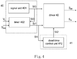
- Fig. 4 is an explanatory diagram showing a schematic of a control device in the flyback converter according to the present disclosure
- Fig. 5 is an explanatory diagram showing a schematic of a timer in Fig. 4
- Fig. 6 is an explanatory diagram showing a schematic of a dead-time control unit in Fig. 4 .
- the control device in the flyback converter includes a first operation means 40 and a second operation means 41.
- the first voltage signal represents a signal according to an input voltage of the flyback converter
- the second voltage signal represents a signal according to an output voltage of the flyback converter.
- the first operation means includes a signal unit 401 and a timer 402.
- the signal unit 401 is configured to generate the third control signal SI3, wherein the third control signal SI3 is used for turning on the auxiliary switch S2.
- the signal unit 401 can be, but not be limited to, configured to generate the third control signal SI3 at the time when the magnetizing current of the flyback converter returns to zero.
- the timer 402 receives the first voltage signal, the second voltage signal and the third control signal SI3, and outputs a first control signal SI1 to the controller 41, wherein the first control signal SI1 is used for turning off the auxiliary switch.
- the second operation means 41 includes a dead-time control unit 412.
- the dead-time control unit 412 receives the first control signal SI1 and outputs a second control signal SI2 according to the first control signal SI1 and the dead time t delay so as to turn on the main switch S1 at ZVS (zero-voltage switching) condition.
- the dead time t delay is constant.
- control device can further include a driver 42.
- the controller 42 is configured to receive the third control signal SI3 and the first control signal SI1, and to output the first drive signal Ssw.
- the first drive signal Ssw with a first level or a first edge is generated by the third control signal SI3 to turn on the auxiliary switch S2.
- the first drive signal Ssw with a second level or a second edge is generated by the first control signal SI1 to turn off the auxiliary switch S2.
- the controller 41 may also output a second drive signal Sm according to second control signal SI2, so as to turn on the main switch S1.
- the driver can be for example but not limited to a RS flip-flop.
- sampling means configured to output a third control signal SI3.
- the sampling means for obtaining a first voltage signal and a second voltage signal, the first voltage signal representing an input voltage of the flyback converter, and the second voltage signal representing an output voltage of the flyback converter.
- the sampling means can directly obtain the first voltage signal and the second voltage signal by sampling the voltage at the input terminal and output terminal of the flyback converter respectively.
- the sampling means can indirectly obtain the first voltage signal and the second voltage signal by sampling a negative voltage at an auxiliary winding T3 of the transformer T and a positive voltage at the auxiliary winding T3 respectively.
- the synchronous rectifier switch SR may act as the auxiliary switch of the flyback converter and the sampling means can directly obtain the first voltage signal by sampling the voltage across the synchronous rectifier switch under off-state condition.
- the timer 402 includes a current-signal output module 311, a first capacitor C1, a first control switch K1, and a comparison module 312.
- the first capacitor C1 has a first terminal electrically connected to the current-signal output module 311, and a second terminal being grounded.
- the first control switch K1 is connected to the first capacitor C1 in parallel, and may be turned off depending on the third control signal SI3.
- the comparison module 312 has a first input terminal electrically connected to the first terminal of the first capacitor C1 and the current-signal output module 311, and a second input terminal for receiving the reference voltage V ref , wherein the reference voltage V ref is a voltage corresponding to a voltage of the first voltage signal V bus .
- the reference voltage may be a sampling voltage of the first voltage signal V bus .
- the current-signal output module 311 outputs a current signal according to the second voltage signal (e.g., Vo in Fig. 5 ) by using a proportional coefficient.
- the first control switch K1 is turned off according to the third control signal SI3
- the first capacitor C1 enters a charging state in which the first capacitor C1 is charged with the current signal.
- the comparison module 312 compares the reference voltage V ref with the voltage at the first capacitor C1. When the voltage at the first capacitor C1 is the same as the reference voltage V ref , the comparison module 312 outputs the first control signal SI1, so as to turn off the auxiliary switch S2. And then the first capacitor ends the charging state.
- the turn-on time t on is the charging time of the first capacitor.
- the proportional coefficient used by the current-signal output module 311 may be obtained according to the above-mentioned Equation 1.
- the turn-on time t on may be obtained according to the above-mentioned Equation 2.
- Fig. 6 is an explanatory diagram showing a schematic of a dead-time control unit in Fig. 4 .
- the dead-time control unit 412 includes a dead-time obtaining module 321 and a second-control-signal output module 322.
- the dead-time obtaining module 321 obtains the dead time t delay .
- the second-control-signal output module 322 is electrically connected to the dead-time obtaining module 321.
- the second control signal SI2 is generated at a time delayed for duration of the dead time t delay after the generation of the first control signal SI1, so that the main switch S1 is turned on.
- the dead-time obtaining module 321 is a time delayer, but the present invention is not limited thereto.
- the dead time t delay may be obtained according to the above-mentioned Equation 3.
- Fig. 7 is a waveform diagram of the flyback converter according to the present disclosure.
- Figs. 8-9 are ZVS resonant state planes of the flyback converter under different load conditions by using the control method according to the present disclosure. Below, principles of a method and an apparatus for controlling the auxiliary switch of the flyback converter in the present disclosure will be described in detail with reference to Fig. 1 and Figs. 7-9 .
- the turn-on time t on of the auxiliary switch S2 in the present disclosure may be obtained according to the above-mentioned Equation 2.
- Equation 2 although the turn-on time t on of the auxiliary switch S2 is still relevant to the input voltage and the output voltage, the relationship between them becomes a simple proportional relation. Therefore, the turn-on time t on of the auxiliary switch S2 may be easily regulated according to the circuit parameters of the flyback circuit.
- t0-t1 is the duration of the turn-on time t on of the auxiliary switch S2, while t1-t2 is the duration of the dead time t delay .
- the auxiliary switch S2 is turned on, such that a voltage nV o is applied to the inductor L1 in the transformer T so as to generate the magnetizing current I m .
- the auxiliary switch S2 is turned off, such that the inductor L1 and the parasitic capacitance C2 resonate.
- the source-drain voltage V DS of the main switch S1 starts to decrease.
- the main switch S1 is turned on. In this way, ZVS may be achieved.
- Figs. 8-9 are resonant state planes of the flyback converter when V bus is greater than n ⁇ V o , and when V bus is less than or equal to n ⁇ V o , respectively.
- the horizontal axis indicates a voltage V Ceq of the parasitic capacitance C2, which is equivalent to the source-drain voltage V DS of the main switch S1.
- the vertical axis indicates a product of the magnetizing current I m and a characteristic impedance Z.
- the auxiliary switch S2 is turned on.
- the voltage at C2 is Vbus+nV o .
- the magnetizing current I m starts to negatively increase from 0.
- the product of the magnetizing current I m and the characteristic impedance Z reaches Vbus.
- the auxiliary switch S2 is turned off.
- the inductor L1 and the parasitic capacitance Ceq start to resonate.
- the voltage at C2 becomes equivalent to the source-drain voltage V DS .
- V DS is 0.
- Figs. 8 and 9 there are three dots on the horizontal axis which represent a light load, a moderate load and a heavy load, respectively, along a direction of the horizontal axis.
- the duration from t1 to t2 i.e., the dead time
- Equation 3 the duration from t1 to t2 (i.e., the dead time) is a quarter of the resonant cycle, and may be expressed by the above-mentioned Equation 3.
- the previous embodiment is described by taking an active clamp flyback converter shown in Fig. 1 as an example, in which the auxiliary switch is a clamp switch in the active clamp flyback converter.
- the present invention is not limited thereto.
- the control method and apparatus according to the present disclosure may be alternatively applied to flyback converters of other schematics.
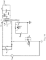
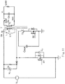
- the flyback converter may further include an auxiliary winding T3, an auxiliary switch S2 and an auxiliary capacitance Caux.
- the auxiliary switch S2, the auxiliary capacitance Caux and the auxiliary winding T3 are connected in series.
- principles and operations of the control method and the control apparatus of the flyback converter are the same as those in the previous embodiments. Accordingly, detailed description is omitted.
- the auxiliary switch may be a synchronous rectifier switch SR.
- Principles and operations of the control method and the control apparatus of the flyback converter are almost the same as those in the previous embodiments, except that the first voltage signal may be obtained by sampling a voltage at the synchronous rectifier switch SR.
- the present invention may provide a constant dead time in the flyback converter by setting the turn-on time of the auxiliary switch. Additionally, the present invention may implement zero-voltage-switching (ZVS) of the main switch within a full range of loads at different output voltages with respect to a full range of input voltage (e.g., 90 ⁇ 264Vac), and may implement optimized designs efficiently.
- ZVS zero-voltage-switching
Landscapes
- Engineering & Computer Science (AREA)
- Power Engineering (AREA)
- Dc-Dc Converters (AREA)
Abstract
Description
- The present invention relates to a method and an apparatus for controlling a flyback converter, and specifically to a method and an apparatus for controlling a flyback converter suitable for applications with variable output voltages.
- A flyback converter is a preferred topology for adapters due to its simple circuit schematic. However, its switching frequency is limited by turn-on losses of the main switch in the flyback converter. A conventional method for reducing the turn-on losses of the main switch is to achieve zero-voltage-switching (ZVS) of the main switch. The ZVS may be achieved by turning on an auxiliary switch for duration of time before the turn on of the main switch. The auxiliary switch may be an active clamp switch, or a switch connected to an auxiliary winding in series or a synchronous rectifier switch.
- In a conventional control scheme, a turn-on time of the auxiliary switch, and a dead time between the auxiliary switch and the main switch are both constant. However, such a control scheme is not suitable for applications with variable output voltages, which is the requirement of Universal Serial Bus Power Delivery (USB PD) in the future. Therefore, in order to optimize efficiency, the turn-on time of the auxiliary switch and the dead time are required to be variable in response to variations of an input voltage and an output voltage, thereby increasing the complexity of the controller. Moreover, with increasing switch frequency, the dead time becomes relatively smaller. Consequently, transmission delay and parameter tolerance of the controller become a huge obstacle for controlling variable dead time.
- Therefore, there is a requirement for providing a method and an apparatus for controlling a flyback converter in order to solve the drawbacks of the conventional technologies.
- In order to overcome the above-mentioned problems existing in the prior art, one aspect of the present disclosure is to provide a method for controlling a flyback converter, the flyback converter including a main switch, a transformer and an auxiliary switch. The method comprises: obtaining a first voltage signal and a second voltage signal, the first voltage signal representing an input voltage of the flyback converter, and the second voltage signal representing an output voltage of the flyback converter; controlling turn-on of the auxiliary switch, wherein the turn-on time period of the auxiliary switch is determined according to the first voltage signal and the second voltage signal; turning on the main switch at ZVS condition, wherein the main switch is turned on at the time delayed for a duration of a dead time after turning off of the auxiliary switch.
- Another aspect of the present disclosure is to provide an apparatus for controlling a flyback converter, the flyback converter including a main switch, a transformer and an auxiliary switch. The apparatus comprises: a sampling means for obtaining a first voltage signal and a second voltage signal, the first voltage signal representing an input voltage of the flyback converter, and the second voltage signal representing an output voltage of the flyback converter; a first operation means for controlling turn-on of the auxiliary switch, wherein a turn-on time period of the auxiliary switch is determined according to the first voltage signal and the second voltage signal; and a second operation means for turning on the main switch at ZVS condition, wherein the main switch is turned on at the time delayed for a duration of a dead time after turning off of the auxiliary switch.
-
-
Fig. 1 is an explanatory diagram showing a circuit schematic of a flyback converter according to a first embodiment of the present disclosure. -
Fig. 2 is a flow chart showing a method for controlling the flyback converter according to an embodiment of the present disclosure. -
Fig. 3a is a flow chart showing steps of the method inFig. 2 . -
Fig. 3b is a flow chart showing steps of the method inFig. 3a . -
Fig. 4 is an explanatory diagram showing a schematic of a control device in the flyback converter according to the present disclosure. -
Fig. 5 is an explanatory diagram showing a schematic of a timer inFig. 4 . -
Fig. 6 is an explanatory diagram showing a schematic of a dead-time control unit inFig. 4 . -
Fig. 7 is a waveform diagram of the flyback converter according to the present disclosure. -
Figs. 8-9 are ZVS resonant state planes of the flyback converter under different load conditions by using the control method according to the present disclosure. -
Fig. 10 is an explanatory diagram showing a circuit schematic of a flyback converter according to a second embodiment of the present disclosure. -
Fig. 11 is an explanatory diagram showing a circuit schematic of a flyback converter according to a third embodiment of the present disclosure. - The present disclosure will be further described in detail with reference to the accompanying drawings and embodiments. Those embodiments are implemented according to the technical ideas of the present disclosure. Although specific configuration and processes are described in those embodiments, the protection extent of the present disclosure is not limited thereto.
- Referring to
Figs. 1-3b ,Fig. 1 is an explanatory diagram showing a circuit schematic of a flyback converter according to a first embodiment of the present disclosure;Fig. 2 is a flow chart showing a method for controlling the flyback converter;Fig. 3a is a flow chart showing steps of the method inFig. 2 ; andFig. 3b is a flow chart showing steps of the method inFig. 3a . - As shown in
Fig. 1 , the flyback converter includes a main switch S1, a transformer T, and an auxiliary switch S2. The transformer T includes a primary winding T1 and a secondary winding T2. The main switch S1 has a first terminal electrically connected to a primary winding T1 of the transformer T, and a second terminal being grounded. The auxiliary switch S2 is a clamp switch in the active clamp flyback converter, and is connected to the primary winding T1 of the transformer T in parallel. In one embodiment, an inductor L1 may be an inductor of the primary winding T1. - As shown in
Fig. 2 , the method for controlling the flyback converter according to the present disclosure includes: - Step 201: obtaining a first voltage signal and a second voltage signal, the first voltage signal representing an input voltage Vbus of the flyback converter, and the second voltage signal representing an output voltage Vo of the flyback converter;
- Step 202: controlling turn-on of the auxiliary switch S2, wherein the turn-on time period ton of the auxiliary switch S2 is determined according to the first voltage signal and the second voltage signal;
- Step 203: turning on the main switch at ZVS condition S1, wherein the main switch S1 is turned on at the time delayed for a duration of a dead time tdelay after turning off of the auxiliary switch S2. In some embodiments, the dead time tdelay may be constant.
- In this embodiment, the first voltage signal and the second voltage signal are obtained directly by sampling voltages at an input terminal and an output terminal of the flyback converter respectively in Step 201, but the present invention is not limited thereto. In other embodiments, the first voltage signal and the second voltage signal may be obtained indirectly. For example, as shown in
Figs. 10-11 , the first voltage signal may be obtained by sampling a negative voltage at an auxiliary winding T3 of the transformer T, and the second voltage signal may be obtained by sampling a positive voltage at the auxiliary winding T3 in Step 201. In still other embodiment, the synchronous rectifier switch SR may act as the auxiliary switch of the flyback converter and the first voltage signal may be obtained by sampling the voltage across the synchronous rectifier switch under off-state condition. Specific methods for obtaining the first voltage signal and the second voltage signal are not limited in the present invention, and may be designed by those skilled in the art as necessary. - Further, as shown in
Fig.3a ,step 202 may further include: - Step 202-1: generating a third control signal and turning on the auxiliary switch according to the third control signal;
- Step 202-2: generating a first control signal according to the first voltage signal, the second voltage signal and the third control signal; and
- Step 202-3: turning off the auxiliary switch according to the first control signal.
- In one embodiment, step202 further includes: outputting a first drive signal Ssw according to the third control signal SI3 and the first control signal SI1. The first drive signal Ssw with a first level (for example but not limited to a high level) or a first edge (for example but not limited to a rising edge) is generated according to the first control signal SI1, so as to turn on the auxiliary switch S2. The first drive signal Ssw with a second level (for example but not limited to a low level) or a second edge (for example but not limited to a falling edge) is generated according to the first control signal SI1, so as to turn off the auxiliary switch S2.
- Further, as shown in
Fig.3b , Step 202-2 may further include: - Step 202-21: outputting a current signal according to the second voltage signal Vo by using a proportional coefficient;
- Step 202-22: charging the first capacitor C1 with the current signal after a first capacitor C1 enters a charging state by the third control signal SI3;
- Step 202-23: comparing a reference voltage Vref with a voltage at the first capacitor C1, wherein the reference voltage Vref is a voltage corresponding to a voltage of the first voltage signal Vbus. For example, the reference voltage may be a sampling voltage of the first voltage signal Vbus;
- Step 202-24: outputting the first control signal SI1 and ending the charging state of the first capacitor when the voltage at the first capacitor C1 is the same as the reference voltage Vref. wherein the turn-on time ton is a charging time of the first capacitor.
- Refer to
Fig.2 , Further, in Step 203, the second control signal SI2 is generated at a time delayed for duration of the dead time tdelay after the generation of the first control signal SI1. - Further, in Step 202-2, the proportional coefficient may be obtained according to the following formula:

- Here, C indicates a capacitance value of the first capacitor C1; K indicates the proportional coefficient; Ceq indicates a capacitance value of a parasitic capacitance C2 between the first terminal of the main switch S1 and ground; Lm indicates an inductance value of the inductor L1 of the primary switch; and n indicates a turn ratio of the transformer T.
- In
Step 202, the turn-on time ton may be determined according to the following formula:
- Here, ton indicates the turn-on time of the auxiliary switch, Vbus indicates the voltage of the first voltage signal; Vo indicates the voltage of the second voltage signal; Ceq indicates the capacitance value of the parasitic capacitance C2 between the first terminal of the main switch S1 and the ground; Lm indicates the inductance value of the inductor L1; and n indicates the turn ratio of the transformer T.
- In Step 203, the dead time tdelay may be obtained according to the following formula:

- Here, tdelay indicates the dead time between the turning off of the auxiliary switch S2 and the turning on of the main switch S1, Ceq indicates the capacitance value of the parasitic capacitance C2 between the first terminal of the main switch S1 and ground; and Lm indicates the inductance value of the inductor L1.
- Now referring to
Fig. 1 andFigs. 4-6 ,Fig. 4 is an explanatory diagram showing a schematic of a control device in the flyback converter according to the present disclosure;Fig. 5 is an explanatory diagram showing a schematic of a timer inFig. 4 ; andFig. 6 is an explanatory diagram showing a schematic of a dead-time control unit inFig. 4 . - As shown in
Fig.4 , the control device in the flyback converter according to the present disclosure includes a first operation means 40 and a second operation means 41. - The first operation means 40 for controlling turn-on of the auxiliary switch S2, wherein a turn-on time period ton of the auxiliary switch S2 is determined according to the first voltage signal and the second voltage signal. In one embodiment, the first voltage signal represents a signal according to an input voltage of the flyback converter, and the second voltage signal represents a signal according to an output voltage of the flyback converter.
- The second operation means 41 for turning on the main switch S1 at ZVS condition, wherein the main switch S1 is turned on at the time delayed for a duration of a dead time tdelay after turning off of the auxiliary switch S2.
- As shown in
Fig.4 , the first operation means includes asignal unit 401 and atimer 402. - The
signal unit 401 is configured to generate the third control signal SI3, wherein the third control signal SI3 is used for turning on the auxiliary switch S2. Thesignal unit 401 can be, but not be limited to, configured to generate the third control signal SI3 at the time when the magnetizing current of the flyback converter returns to zero. - The
timer 402 receives the first voltage signal, the second voltage signal and the third control signal SI3, and outputs a first control signal SI1 to thecontroller 41, wherein the first control signal SI1 is used for turning off the auxiliary switch. - Refer to
Fig.4 again, the second operation means 41 includes a dead-time control unit 412. The dead-time control unit 412 receives the first control signal SI1 and outputs a second control signal SI2 according to the first control signal SI1 and the dead time tdelay so as to turn on the main switch S1 at ZVS (zero-voltage switching) condition. Here, the dead time tdelay is constant. - In some embodiment, the control device can further include a
driver 42. Thecontroller 42 is configured to receive the third control signal SI3 and the first control signal SI1, and to output the first drive signal Ssw. The first drive signal Ssw with a first level or a first edge is generated by the third control signal SI3 to turn on the auxiliary switch S2. And the first drive signal Ssw with a second level or a second edge is generated by the first control signal SI1 to turn off the auxiliary switch S2. - In this embodiment, the
controller 41 may also output a second drive signal Sm according to second control signal SI2, so as to turn on the main switch S1. - In some embodiment, the driver can be for example but not limited to a RS flip-flop.
- In one embodiment, there is also a sampling means (not shown) configured to output a third control signal SI3. The sampling means for obtaining a first voltage signal and a second voltage signal, the first voltage signal representing an input voltage of the flyback converter, and the second voltage signal representing an output voltage of the flyback converter.
- In one embodiment, the sampling means can directly obtain the first voltage signal and the second voltage signal by sampling the voltage at the input terminal and output terminal of the flyback converter respectively. In other embodiment, the sampling means can indirectly obtain the first voltage signal and the second voltage signal by sampling a negative voltage at an auxiliary winding T3 of the transformer T and a positive voltage at the auxiliary winding T3 respectively. In still other embodiment, the synchronous rectifier switch SR may act as the auxiliary switch of the flyback converter and the sampling means can directly obtain the first voltage signal by sampling the voltage across the synchronous rectifier switch under off-state condition.
- Further, as shown in
Fig. 5 , thetimer 402 includes a current-signal output module 311, a first capacitor C1, a first control switch K1, and acomparison module 312. The first capacitor C1 has a first terminal electrically connected to the current-signal output module 311, and a second terminal being grounded. The first control switch K1 is connected to the first capacitor C1 in parallel, and may be turned off depending on the third control signal SI3. Thecomparison module 312 has a first input terminal electrically connected to the first terminal of the first capacitor C1 and the current-signal output module 311, and a second input terminal for receiving the reference voltage Vref, wherein the reference voltage Vref is a voltage corresponding to a voltage of the first voltage signal Vbus. For example, the reference voltage may be a sampling voltage of the first voltage signal Vbus. - The current-
signal output module 311 outputs a current signal according to the second voltage signal (e.g., Vo inFig. 5 ) by using a proportional coefficient. When the first control switch K1 is turned off according to the third control signal SI3, the first capacitor C1 enters a charging state in which the first capacitor C1 is charged with the current signal. - The
comparison module 312 compares the reference voltage Vref with the voltage at the first capacitor C1. When the voltage at the first capacitor C1 is the same as the reference voltage Vref, thecomparison module 312 outputs the first control signal SI1, so as to turn off the auxiliary switch S2. And then the first capacitor ends the charging state. The turn-on time ton is the charging time of the first capacitor. - In this embodiment, the proportional coefficient used by the current-
signal output module 311 may be obtained according to the above-mentionedEquation 1. - Further, in this embodiment, the turn-on time ton may be obtained according to the above-mentioned
Equation 2. -
Fig. 6 is an explanatory diagram showing a schematic of a dead-time control unit inFig. 4 . As shown inFig. 6 , the dead-time control unit 412 includes a dead-time obtaining module 321 and a second-control-signal output module 322. The dead-time obtaining module 321 obtains the dead time tdelay. The second-control-signal output module 322 is electrically connected to the dead-time obtaining module 321. The second control signal SI2 is generated at a time delayed for duration of the dead time tdelay after the generation of the first control signal SI1, so that the main switch S1 is turned on. In this embodiment, the dead-time obtaining module 321 is a time delayer, but the present invention is not limited thereto. - In this embodiment, the dead time tdelay may be obtained according to the above-mentioned Equation 3.
-
Fig. 7 is a waveform diagram of the flyback converter according to the present disclosure.Figs. 8-9 are ZVS resonant state planes of the flyback converter under different load conditions by using the control method according to the present disclosure. Below, principles of a method and an apparatus for controlling the auxiliary switch of the flyback converter in the present disclosure will be described in detail with reference toFig. 1 andFigs. 7-9 . - In order to achieve the ZVS of the main switch S1 in the flyback converter, it is necessary that the auxiliary switch S2 has been turned on for duration of time before the main switch S1 is turned on, so as to generate a negative magnetizing current. In order to allow a source-drain voltage VDS of the main switch S1 down to zero with the amplitude of the generated magnetizing current, it is required that the turn-on time ton of the auxiliary switch S2 and the corresponding dead time tdelay satisfy the following formula, respectively:


- Here, θ is a phase angle, and may satisfy the following formulas:


- From the above formulas, it may be understood that, in the prior art, the turn-on time of the auxiliary switch and the corresponding dead time need to be adjusted according to the input voltage and the output voltage. The control is complicated and is especially not suitable for the high frequency design.
- In contrast, the turn-on time ton of the auxiliary switch S2 in the present disclosure may be obtained according to the above-mentioned
Equation 2. Referring toEquation 2, although the turn-on time ton of the auxiliary switch S2 is still relevant to the input voltage and the output voltage, the relationship between them becomes a simple proportional relation. Therefore, the turn-on time ton of the auxiliary switch S2 may be easily regulated according to the circuit parameters of the flyback circuit. - Additionally, according to the above turn-on time ton of the auxiliary switch S2, the above-mentioned Equation 3 for the corresponding dead time tdelay may be obtained.
- As shown in
Fig. 7 , t0-t1 is the duration of the turn-on time ton of the auxiliary switch S2, while t1-t2 is the duration of the dead time tdelay. According to the method and the apparatus for controlling an auxiliary switch in the present disclosure, at time t0, the auxiliary switch S2 is turned on, such that a voltage nVo is applied to the inductor L1 in the transformer T so as to generate the magnetizing current Im. Then, at time t1, the auxiliary switch S2 is turned off, such that the inductor L1 and the parasitic capacitance C2 resonate. As a result, the source-drain voltage VDS of the main switch S1 starts to decrease. With the aid of the magnetizing current Im, the voltage VDS is decreased to zero at time t2. At time t2, the main switch S1 is turned on. In this way, ZVS may be achieved. -
Figs. 8-9 are resonant state planes of the flyback converter when Vbus is greater than n∗Vo, and when Vbus is less than or equal to n∗Vo, respectively. Here, the horizontal axis indicates a voltage VCeq of the parasitic capacitance C2, which is equivalent to the source-drain voltage VDS of the main switch S1. The vertical axis indicates a product of the magnetizing current Im and a characteristic impedance Z. - Referring to
Fig. 7 andFigs. 8-9 , at time t0, the auxiliary switch S2 is turned on. The voltage at C2 is Vbus+nVo. The magnetizing current Im starts to negatively increase from 0. Then, at time t1, the product of the magnetizing current Im and the characteristic impedance Z reaches Vbus. The auxiliary switch S2 is turned off. Then, starting from time t1, the inductor L1 and the parasitic capacitance Ceq start to resonate. Then, at time t2, the voltage at C2 becomes equivalent to the source-drain voltage VDS. At this time, VDS is 0. - As can be seen from the state locus diagram from t1 to t2, there is an arched trace with a radian of π/2. Further, a resonant period of the inductor L1 and the parasitic capacitance C2 may be expressed as

- Referring to
Figs. 8 and 9 again, there are three dots on the horizontal axis which represent a light load, a moderate load and a heavy load, respectively, along a direction of the horizontal axis. As can be seen, in any case of the above three loads, it is ensured that the duration from t1 to t2 (i.e., the dead time) is a quarter of the resonant cycle, and may be expressed by the above-mentioned Equation 3. - The previous embodiment is described by taking an active clamp flyback converter shown in
Fig. 1 as an example, in which the auxiliary switch is a clamp switch in the active clamp flyback converter. However, the present invention is not limited thereto. The control method and apparatus according to the present disclosure may be alternatively applied to flyback converters of other schematics. For example, as shown inFigs. 10 and11 , the flyback converter may further include an auxiliary winding T3, an auxiliary switch S2 and an auxiliary capacitance Caux. The auxiliary switch S2, the auxiliary capacitance Caux and the auxiliary winding T3 are connected in series. In this embodiment, principles and operations of the control method and the control apparatus of the flyback converter are the same as those in the previous embodiments. Accordingly, detailed description is omitted. In other application, the auxiliary switch may be a synchronous rectifier switch SR. Principles and operations of the control method and the control apparatus of the flyback converter are almost the same as those in the previous embodiments, except that the first voltage signal may be obtained by sampling a voltage at the synchronous rectifier switch SR. - The present invention may provide a constant dead time in the flyback converter by setting the turn-on time of the auxiliary switch. Additionally, the present invention may implement zero-voltage-switching (ZVS) of the main switch within a full range of loads at different output voltages with respect to a full range of input voltage (e.g., 90∼264Vac), and may implement optimized designs efficiently.
- Note that the above embodiments are only used to illustrate the present disclosure but not to limit the technical solution described in the present disclosure. Moreover, although the present disclosure is described in detail with reference to the above embodiments in this specification, the ordinary persons skilled in the art should understand that modifications or equivalent substitutions may also be made to the present disclosure. Therefore, all the technical solutions not departing from the spirit and scope of the present application and the improvements thereof should be covered by the protection scope of the appended claims in the present application.
Claims (27)
- A method for controlling a flyback converter, the flyback converter including a main switch, a transformer and an auxiliary switch, the method comprising:obtaining a first voltage signal and a second voltage signal, the first voltage signal representing an input voltage of the flyback converter, and the second voltage signal representing an output voltage of the flyback converter (S201);controlling turn-on of the auxiliary switch, wherein the turn-on time period of the auxiliary switch is determined according to the first voltage signal and the second voltage signal (S202); andturning on the main switch at ZVS condition, wherein the main switch is turned on at the time delayed for a duration of a dead time after turning off of the auxiliary switch (S203).
- The control method according to claim 1, wherein
the auxiliary switch is an active clamp switch for the flyback converter, or
the transformer further comprises an auxiliary winding connected to the auxiliary switch in series, or
the flyback converter further comprises a synchronous rectifier switch as the auxiliary switch. - The control method according to claim 2, wherein the first voltage signal is obtained by sampling a negative voltage at the auxiliary winding, and the second voltage signal is obtained by sampling a positive voltage at the auxiliary winding.
- The control method according to claim 2, wherein the first voltage signal is obtained by sampling a voltage across the synchronous rectifier switch under off-state condition.
- The control method according to claim 1, controlling turn-on of the auxiliary switch (S202) further comprising:outputting a current signal according to the second voltage signal by using a proportional coefficient (S202-21); andcharging the first capacitor with the current signal until a voltage across the first capacitor is equal to a reference voltage, wherein the reference voltage is a voltage corresponding to the first voltage signal (S202-22);wherein the turn-on time period is a charging time of the first capacitor.
- The control method according to claim 1, wherein the turn-on time period is determined according to the following formula:

- The control method according to claim 1, wherein the dead time is constant.
- The control method according to claim 7, wherein the dead time is determined according to the following formula:

- The control method according to claim 1, wherein controlling turn-on of the auxiliary switch (S202) further comprises:generating a third control signal and turning on the auxiliary switch according to the third control signal (S202-1);generating a first control signal according to the first voltage signal, the second voltage signal and the third control signal (S202-2); andturning off the auxiliary switch according to the first control signal (S202-3).
- The control method according to claim 9, wherein turning on the main switch (S203) further comprises:
outputting a second control signal according to the first control signal and the dead time and turning on the main switch at a zero-voltage switching condition according to the second control signal. - The control method according to claim 9, generating the first control signal according to the first voltage signal, the second voltage signal and the third control signal (S202-2) further comprising:outputting a current signal according to the second voltage signal by using a proportional coefficient (S202-21);charging the first capacitor with the current signal after a first capacitor enters a charging state by the third control signal (S202-22);comparing a reference voltage with a voltage at the first capacitor (S202-23); andoutputting the first control signal and ending the charging state of the first capacitor when the voltage at the first capacitor is the same as the reference voltage, wherein the reference voltage is a voltage corresponding to the first voltage signal (S202-24).
- The control method according to claim 11, wherein the main switch has a first terminal electrically connected to a primary winding of the transformer, and a second terminal being grounded, and
the proportional coefficient is obtained according to the following formula:
- The control method according to claim 9, wherein controlling turn-on of the auxiliary switch (S202) further comprising:outputting a first drive signal with a first level or a first edge according to the third control signal and turning on the auxiliary switch according to the first drive signal with the first level or a first edge; andoutputting the first drive signal with a second level or a second edge according to the first control signal and turning off the auxiliary switch according to the first drive signal with the second level or a second edge.
- An apparatus for controlling a flyback converter, the flyback converter including a main switch (S1), a transformer (T) and an auxiliary switch (S2), the apparatus comprising:a sampling means for obtaining a first voltage signal and a second voltage signal, the first voltage signal representing an input voltage of the flyback converter, and the second voltage signal representing an output voltage of the flyback converter;a first operation means (40) for controlling turn-on of the auxiliary switch (S2), wherein a turn-on time period ton of the auxiliary switch (S2) is determined according to the first voltage signal and the second voltage signal; anda second operation means (41) for turning on the main switch (S1) at ZVS condition, wherein the main switch (S1) is turned on at the time delayed for a duration of a dead time after turning off of the auxiliary switch (S2).
- The apparatus according to claim 14, wherein
the auxiliary switch (S2) is an active clamp switch in the flyback converter, or
the transformer (T) further comprises an auxiliary winding (T3) connected to the auxiliary switch (S2) in series, or
the flyback converter further comprises a synchronous rectifier switch as the auxiliary switch (S2). - The apparatus according to claim 14, wherein the sampling means obtains the first voltage signal and the second voltage signal by sampling voltages at an input terminal and an output terminal of the flyback converter respectively.
- The apparatus according to claim 15, wherein the sampling means obtains the first voltage signal by sampling a negative voltage at the auxiliary winding (T3), and obtains the second voltage signal by sampling a positive voltage at the auxiliary winding (T3).
- The apparatus according to claim 15, wherein the sampling means obtains the first voltage signal by sampling a voltage across the synchronous rectifier switch under off-state condition.
- The apparatus according to claim 14, wherein the turn-on time period is determined according to the following formula:

- The apparatus according to claim 14, wherein the dead time is constant.
- The apparatus according to claim 20, wherein the dead time is determined according to the following formula:

- The apparatus according to claim 14, wherein the first operation means (40) comprises:a signal unit (401) configured to generate a third control signal SI3, wherein the third control signal SI3 is used for turning on the auxiliary switch (S2); anda timer (402) configured to receive a first voltage signal, a second voltage signal and the third control signal SI3, and to output a first control signal SI1, wherein the first control signal SI1 is used for turning off the auxiliary switch (S2).
- The apparatus according to claim 22, wherein the timer (402) comprises:a current-signal output module (311) configured to output a current signal according to the second voltage signal by using a proportional coefficient;a first capacitor (C1) having a first terminal electrically connected to the current-signal output module (311), and a second terminal being grounded;a first control switch (K1) electrically connected to the first capacitor (C1) in parallel and configured to control the first capacitor (C1) to enter a charging state by the third control signal SI3; anda comparison module (312) having a first input terminal electrically connected to the first terminal of the first capacitor (C1), and a second input terminal for receiving a reference voltage corresponding to the first voltage signal, the comparison module (312) being configured to compare the reference voltage with a voltage at the first capacitor (C1);wherein the comparison module (312) is configured to output the first control signal and the first capacitor (C1) ends the charging state when the voltage at the first capacitor (C1) is the same as the reference voltage; andwherein the turn-on time period is a charging time of the first capacitor (C1).
- The apparatus according to claim 23, wherein the main switch (S1) has a first terminal electrically connected to a primary winding (T1) of the transformer (T), and a second terminal being grounded, and
the proportional coefficient is obtained according to the following formula:
- The apparatus according to claim 22, wherein the second operation means (41) comprises:
a dead-time control unit (412) configured to receive the first control signal SI1, and to output a second control signal SI2 according to the first control signal SI1 and the dead time, wherein the second control signal SI2 is used for turning on the main switch (S1) at a zero-voltage switching condition. - The apparatus according to claim 25, wherein the dead-time control unit (412) comprises:a dead-time obtaining module (321) configured to obtain the dead time; anda second-control-signal output module (322) electrically connected to the dead-time obtaining module (321), and configured to receive the first control signal SI1 and the dead-time and to output a second control signal SI2.
- The apparatus according to claim 22, wherein the apparatus further comprises:
a driver (42) configured to receive the third control signal SI3 and the first control signal SI1, and to output the first drive signal SSW, wherein the first drive signal SSW with a first level or a first edge is generated by the third control signal SI3 to turn on the auxiliary switch (S2) and the first drive signal SSW with a second level or a second edge is generated by the first control signal SI1 to turn off the auxiliary switch (S2).
Applications Claiming Priority (2)
| Application Number | Priority Date | Filing Date | Title |
|---|---|---|---|
| CN201810718910 | 2018-07-03 | ||
| CN201910544717.5A CN110677013B (en) | 2018-07-03 | 2019-06-21 | Control method and device of flyback converter |
Publications (2)
| Publication Number | Publication Date |
|---|---|
| EP3591826A1 true EP3591826A1 (en) | 2020-01-08 |
| EP3591826B1 EP3591826B1 (en) | 2021-02-24 |
Family
ID=67145561
Family Applications (1)
| Application Number | Title | Priority Date | Filing Date |
|---|---|---|---|
| EP19183833.3A Active EP3591826B1 (en) | 2018-07-03 | 2019-07-02 | Method and apparatus for controlling a flyback converter |
Country Status (1)
| Country | Link |
|---|---|
| EP (1) | EP3591826B1 (en) |
Cited By (1)
| Publication number | Priority date | Publication date | Assignee | Title |
|---|---|---|---|---|
| CN116207995A (en) * | 2023-03-07 | 2023-06-02 | 杭州茂力半导体技术有限公司 | Flyback circuit, auxiliary switch control circuit for flyback circuit and control method |
Citations (5)
| Publication number | Priority date | Publication date | Assignee | Title |
|---|---|---|---|---|
| US20050073861A1 (en) * | 2003-10-04 | 2005-04-07 | Delta Electronics, Inc. | Active resonant snubber for dc-dc converter |
| US20150003121A1 (en) * | 2013-06-27 | 2015-01-01 | System General Corporation | Control circuit for active-clamp flyback power converter with programmable switching period |
| EP3107199A1 (en) * | 2015-06-15 | 2016-12-21 | Apple Inc. | Systems and methods of operation for power converters having series-parallel mode active clamps |
| US20170264206A1 (en) * | 2016-03-12 | 2017-09-14 | Fairchild Korea Semiconductor Ltd. | Active clamp flyback converter |
| US20180062529A1 (en) * | 2016-08-31 | 2018-03-01 | Delta Electronics, Inc. | Converter and control method thereof |
-
2019
- 2019-07-02 EP EP19183833.3A patent/EP3591826B1/en active Active
Patent Citations (5)
| Publication number | Priority date | Publication date | Assignee | Title |
|---|---|---|---|---|
| US20050073861A1 (en) * | 2003-10-04 | 2005-04-07 | Delta Electronics, Inc. | Active resonant snubber for dc-dc converter |
| US20150003121A1 (en) * | 2013-06-27 | 2015-01-01 | System General Corporation | Control circuit for active-clamp flyback power converter with programmable switching period |
| EP3107199A1 (en) * | 2015-06-15 | 2016-12-21 | Apple Inc. | Systems and methods of operation for power converters having series-parallel mode active clamps |
| US20170264206A1 (en) * | 2016-03-12 | 2017-09-14 | Fairchild Korea Semiconductor Ltd. | Active clamp flyback converter |
| US20180062529A1 (en) * | 2016-08-31 | 2018-03-01 | Delta Electronics, Inc. | Converter and control method thereof |
Cited By (2)
| Publication number | Priority date | Publication date | Assignee | Title |
|---|---|---|---|---|
| CN116207995A (en) * | 2023-03-07 | 2023-06-02 | 杭州茂力半导体技术有限公司 | Flyback circuit, auxiliary switch control circuit for flyback circuit and control method |
| CN116207995B (en) * | 2023-03-07 | 2026-03-31 | 杭州茂力半导体技术有限公司 | Flyback circuit, auxiliary switching control circuit for flyback circuit and control method |
Also Published As
| Publication number | Publication date |
|---|---|
| EP3591826B1 (en) | 2021-02-24 |
Similar Documents
| Publication | Publication Date | Title |
|---|---|---|
| US10797603B2 (en) | Method and apparatus for controlling a flyback converter | |
| US11349397B2 (en) | Method and apparatus for controlling a flyback converter | |
| US10333417B2 (en) | Device and method for controlling flyback converter | |
| US10333418B2 (en) | Control device and control method | |
| US10291136B2 (en) | Control device and control method | |
| US8582321B2 (en) | Resonant converters and burst mode control method thereof | |
| EP0761036B1 (en) | Self-oscillating dc to dc converter | |
| EP4148954A1 (en) | Electronic device and control method therefor | |
| CN102801318B (en) | Control circuit and control method of resonant power converter | |
| US11777408B2 (en) | Converter adaptable to wide range output voltage and control method thereof | |
| US10148127B2 (en) | Wireless power transmitting apparatus and method thereof | |
| US20120320633A1 (en) | Variable frequency pwm synchronous rectifier power supply | |
| EP3591826B1 (en) | Method and apparatus for controlling a flyback converter | |
| US9473035B2 (en) | Power conversion device | |
| US11283360B2 (en) | Converter | |
| EP4064540B1 (en) | Control circuit, control method and power converter | |
| CN116742958A (en) | Primary-side control circuit and primary-side control method of flyback converter | |
| Zhou et al. | Wide ZVS operation of a semi‐dual‐bridge resonant converter under variable‐frequency phase‐shift control | |
| CN210405095U (en) | Detection circuit, switch control circuit and flyback conversion circuit | |
| US12261515B2 (en) | Circuit control method and apparatus | |
| US20240006990A1 (en) | Power supply device, resonant converter circuit and controlling method thereof | |
| CN103888011B (en) | Controller and controlling system and method for hiccup-mode driving signals | |
| CN114710044B (en) | Flyback converter and constant current control method thereof | |
| US11527963B2 (en) | Control unit for improving conversion efficiency | |
| CN113193753B (en) | Synchronous rectifying device and receiving end module of wireless charging system |
Legal Events
| Date | Code | Title | Description |
|---|---|---|---|
| PUAI | Public reference made under article 153(3) epc to a published international application that has entered the european phase |
Free format text: ORIGINAL CODE: 0009012 |
|
| STAA | Information on the status of an ep patent application or granted ep patent |
Free format text: STATUS: REQUEST FOR EXAMINATION WAS MADE |
|
| 17P | Request for examination filed |
Effective date: 20190702 |
|
| AK | Designated contracting states |
Kind code of ref document: A1 Designated state(s): AL AT BE BG CH CY CZ DE DK EE ES FI FR GB GR HR HU IE IS IT LI LT LU LV MC MK MT NL NO PL PT RO RS SE SI SK SM TR |
|
| AX | Request for extension of the european patent |
Extension state: BA ME |
|
| RBV | Designated contracting states (corrected) |
Designated state(s): AL AT BE BG CH CY CZ DE DK EE ES FI FR GB GR HR HU IE IS IT LI LT LU LV MC MK MT NL NO PL PT RO RS SE SI SK SM TR |
|
| GRAP | Despatch of communication of intention to grant a patent |
Free format text: ORIGINAL CODE: EPIDOSNIGR1 |
|
| STAA | Information on the status of an ep patent application or granted ep patent |
Free format text: STATUS: GRANT OF PATENT IS INTENDED |
|
| INTG | Intention to grant announced |
Effective date: 20201001 |
|
| GRAS | Grant fee paid |
Free format text: ORIGINAL CODE: EPIDOSNIGR3 |
|
| GRAA | (expected) grant |
Free format text: ORIGINAL CODE: 0009210 |
|
| STAA | Information on the status of an ep patent application or granted ep patent |
Free format text: STATUS: THE PATENT HAS BEEN GRANTED |
|
| AK | Designated contracting states |
Kind code of ref document: B1 Designated state(s): AL AT BE BG CH CY CZ DE DK EE ES FI FR GB GR HR HU IE IS IT LI LT LU LV MC MK MT NL NO PL PT RO RS SE SI SK SM TR |
|
| REG | Reference to a national code |
Ref country code: CH Ref legal event code: EP |
|
| REG | Reference to a national code |
Ref country code: AT Ref legal event code: REF Ref document number: 1365744 Country of ref document: AT Kind code of ref document: T Effective date: 20210315 |
|
| REG | Reference to a national code |
Ref country code: IE Ref legal event code: FG4D |
|
| REG | Reference to a national code |
Ref country code: DE Ref legal event code: R096 Ref document number: 602019002738 Country of ref document: DE |
|
| REG | Reference to a national code |
Ref country code: NL Ref legal event code: FP |
|
| REG | Reference to a national code |
Ref country code: LT Ref legal event code: MG9D |
|
| PG25 | Lapsed in a contracting state [announced via postgrant information from national office to epo] |
Ref country code: BG Free format text: LAPSE BECAUSE OF FAILURE TO SUBMIT A TRANSLATION OF THE DESCRIPTION OR TO PAY THE FEE WITHIN THE PRESCRIBED TIME-LIMIT Effective date: 20210524 Ref country code: HR Free format text: LAPSE BECAUSE OF FAILURE TO SUBMIT A TRANSLATION OF THE DESCRIPTION OR TO PAY THE FEE WITHIN THE PRESCRIBED TIME-LIMIT Effective date: 20210224 Ref country code: GR Free format text: LAPSE BECAUSE OF FAILURE TO SUBMIT A TRANSLATION OF THE DESCRIPTION OR TO PAY THE FEE WITHIN THE PRESCRIBED TIME-LIMIT Effective date: 20210525 Ref country code: FI Free format text: LAPSE BECAUSE OF FAILURE TO SUBMIT A TRANSLATION OF THE DESCRIPTION OR TO PAY THE FEE WITHIN THE PRESCRIBED TIME-LIMIT Effective date: 20210224 Ref country code: LT Free format text: LAPSE BECAUSE OF FAILURE TO SUBMIT A TRANSLATION OF THE DESCRIPTION OR TO PAY THE FEE WITHIN THE PRESCRIBED TIME-LIMIT Effective date: 20210224 Ref country code: NO Free format text: LAPSE BECAUSE OF FAILURE TO SUBMIT A TRANSLATION OF THE DESCRIPTION OR TO PAY THE FEE WITHIN THE PRESCRIBED TIME-LIMIT Effective date: 20210524 Ref country code: PT Free format text: LAPSE BECAUSE OF FAILURE TO SUBMIT A TRANSLATION OF THE DESCRIPTION OR TO PAY THE FEE WITHIN THE PRESCRIBED TIME-LIMIT Effective date: 20210624 |
|
| REG | Reference to a national code |
Ref country code: AT Ref legal event code: MK05 Ref document number: 1365744 Country of ref document: AT Kind code of ref document: T Effective date: 20210224 |
|
| PG25 | Lapsed in a contracting state [announced via postgrant information from national office to epo] |
Ref country code: RS Free format text: LAPSE BECAUSE OF FAILURE TO SUBMIT A TRANSLATION OF THE DESCRIPTION OR TO PAY THE FEE WITHIN THE PRESCRIBED TIME-LIMIT Effective date: 20210224 Ref country code: SE Free format text: LAPSE BECAUSE OF FAILURE TO SUBMIT A TRANSLATION OF THE DESCRIPTION OR TO PAY THE FEE WITHIN THE PRESCRIBED TIME-LIMIT Effective date: 20210224 Ref country code: PL Free format text: LAPSE BECAUSE OF FAILURE TO SUBMIT A TRANSLATION OF THE DESCRIPTION OR TO PAY THE FEE WITHIN THE PRESCRIBED TIME-LIMIT Effective date: 20210224 Ref country code: LV Free format text: LAPSE BECAUSE OF FAILURE TO SUBMIT A TRANSLATION OF THE DESCRIPTION OR TO PAY THE FEE WITHIN THE PRESCRIBED TIME-LIMIT Effective date: 20210224 |
|
| PG25 | Lapsed in a contracting state [announced via postgrant information from national office to epo] |
Ref country code: IS Free format text: LAPSE BECAUSE OF FAILURE TO SUBMIT A TRANSLATION OF THE DESCRIPTION OR TO PAY THE FEE WITHIN THE PRESCRIBED TIME-LIMIT Effective date: 20210624 |
|
| PG25 | Lapsed in a contracting state [announced via postgrant information from national office to epo] |
Ref country code: CZ Free format text: LAPSE BECAUSE OF FAILURE TO SUBMIT A TRANSLATION OF THE DESCRIPTION OR TO PAY THE FEE WITHIN THE PRESCRIBED TIME-LIMIT Effective date: 20210224 Ref country code: EE Free format text: LAPSE BECAUSE OF FAILURE TO SUBMIT A TRANSLATION OF THE DESCRIPTION OR TO PAY THE FEE WITHIN THE PRESCRIBED TIME-LIMIT Effective date: 20210224 Ref country code: AT Free format text: LAPSE BECAUSE OF FAILURE TO SUBMIT A TRANSLATION OF THE DESCRIPTION OR TO PAY THE FEE WITHIN THE PRESCRIBED TIME-LIMIT Effective date: 20210224 Ref country code: SM Free format text: LAPSE BECAUSE OF FAILURE TO SUBMIT A TRANSLATION OF THE DESCRIPTION OR TO PAY THE FEE WITHIN THE PRESCRIBED TIME-LIMIT Effective date: 20210224 |
|
| REG | Reference to a national code |
Ref country code: DE Ref legal event code: R097 Ref document number: 602019002738 Country of ref document: DE |
|
| PG25 | Lapsed in a contracting state [announced via postgrant information from national office to epo] |
Ref country code: DK Free format text: LAPSE BECAUSE OF FAILURE TO SUBMIT A TRANSLATION OF THE DESCRIPTION OR TO PAY THE FEE WITHIN THE PRESCRIBED TIME-LIMIT Effective date: 20210224 Ref country code: RO Free format text: LAPSE BECAUSE OF FAILURE TO SUBMIT A TRANSLATION OF THE DESCRIPTION OR TO PAY THE FEE WITHIN THE PRESCRIBED TIME-LIMIT Effective date: 20210224 Ref country code: SK Free format text: LAPSE BECAUSE OF FAILURE TO SUBMIT A TRANSLATION OF THE DESCRIPTION OR TO PAY THE FEE WITHIN THE PRESCRIBED TIME-LIMIT Effective date: 20210224 |
|
| PLBE | No opposition filed within time limit |
Free format text: ORIGINAL CODE: 0009261 |
|
| STAA | Information on the status of an ep patent application or granted ep patent |
Free format text: STATUS: NO OPPOSITION FILED WITHIN TIME LIMIT |
|
| PG25 | Lapsed in a contracting state [announced via postgrant information from national office to epo] |
Ref country code: AL Free format text: LAPSE BECAUSE OF FAILURE TO SUBMIT A TRANSLATION OF THE DESCRIPTION OR TO PAY THE FEE WITHIN THE PRESCRIBED TIME-LIMIT Effective date: 20210224 Ref country code: ES Free format text: LAPSE BECAUSE OF FAILURE TO SUBMIT A TRANSLATION OF THE DESCRIPTION OR TO PAY THE FEE WITHIN THE PRESCRIBED TIME-LIMIT Effective date: 20210224 |
|
| 26N | No opposition filed |
Effective date: 20211125 |
|
| PG25 | Lapsed in a contracting state [announced via postgrant information from national office to epo] |
Ref country code: SI Free format text: LAPSE BECAUSE OF FAILURE TO SUBMIT A TRANSLATION OF THE DESCRIPTION OR TO PAY THE FEE WITHIN THE PRESCRIBED TIME-LIMIT Effective date: 20210224 |
|
| PG25 | Lapsed in a contracting state [announced via postgrant information from national office to epo] |
Ref country code: MC Free format text: LAPSE BECAUSE OF FAILURE TO SUBMIT A TRANSLATION OF THE DESCRIPTION OR TO PAY THE FEE WITHIN THE PRESCRIBED TIME-LIMIT Effective date: 20210224 |
|
| REG | Reference to a national code |
Ref country code: BE Ref legal event code: MM Effective date: 20210731 |
|
| PG25 | Lapsed in a contracting state [announced via postgrant information from national office to epo] |
Ref country code: IT Free format text: LAPSE BECAUSE OF FAILURE TO SUBMIT A TRANSLATION OF THE DESCRIPTION OR TO PAY THE FEE WITHIN THE PRESCRIBED TIME-LIMIT Effective date: 20210224 |
|
| PG25 | Lapsed in a contracting state [announced via postgrant information from national office to epo] |
Ref country code: IS Free format text: LAPSE BECAUSE OF FAILURE TO SUBMIT A TRANSLATION OF THE DESCRIPTION OR TO PAY THE FEE WITHIN THE PRESCRIBED TIME-LIMIT Effective date: 20210624 Ref country code: LU Free format text: LAPSE BECAUSE OF NON-PAYMENT OF DUE FEES Effective date: 20210702 Ref country code: FR Free format text: LAPSE BECAUSE OF NON-PAYMENT OF DUE FEES Effective date: 20210731 |
|
| PG25 | Lapsed in a contracting state [announced via postgrant information from national office to epo] |
Ref country code: IE Free format text: LAPSE BECAUSE OF NON-PAYMENT OF DUE FEES Effective date: 20210702 Ref country code: BE Free format text: LAPSE BECAUSE OF NON-PAYMENT OF DUE FEES Effective date: 20210731 |
|
| REG | Reference to a national code |
Ref country code: CH Ref legal event code: PL |
|
| PG25 | Lapsed in a contracting state [announced via postgrant information from national office to epo] |
Ref country code: LI Free format text: LAPSE BECAUSE OF NON-PAYMENT OF DUE FEES Effective date: 20220731 Ref country code: CH Free format text: LAPSE BECAUSE OF NON-PAYMENT OF DUE FEES Effective date: 20220731 |
|
| PG25 | Lapsed in a contracting state [announced via postgrant information from national office to epo] |
Ref country code: CY Free format text: LAPSE BECAUSE OF FAILURE TO SUBMIT A TRANSLATION OF THE DESCRIPTION OR TO PAY THE FEE WITHIN THE PRESCRIBED TIME-LIMIT Effective date: 20210224 |
|
| PG25 | Lapsed in a contracting state [announced via postgrant information from national office to epo] |
Ref country code: HU Free format text: LAPSE BECAUSE OF FAILURE TO SUBMIT A TRANSLATION OF THE DESCRIPTION OR TO PAY THE FEE WITHIN THE PRESCRIBED TIME-LIMIT; INVALID AB INITIO Effective date: 20190702 |
|
| GBPC | Gb: european patent ceased through non-payment of renewal fee |
Effective date: 20230702 |
|
| PG25 | Lapsed in a contracting state [announced via postgrant information from national office to epo] |
Ref country code: MK Free format text: LAPSE BECAUSE OF FAILURE TO SUBMIT A TRANSLATION OF THE DESCRIPTION OR TO PAY THE FEE WITHIN THE PRESCRIBED TIME-LIMIT Effective date: 20210224 Ref country code: GB Free format text: LAPSE BECAUSE OF NON-PAYMENT OF DUE FEES Effective date: 20230702 |
|
| PG25 | Lapsed in a contracting state [announced via postgrant information from national office to epo] |
Ref country code: MT Free format text: LAPSE BECAUSE OF FAILURE TO SUBMIT A TRANSLATION OF THE DESCRIPTION OR TO PAY THE FEE WITHIN THE PRESCRIBED TIME-LIMIT Effective date: 20210224 |
|
| PGFP | Annual fee paid to national office [announced via postgrant information from national office to epo] |
Ref country code: NL Payment date: 20250516 Year of fee payment: 7 |
|
| PGFP | Annual fee paid to national office [announced via postgrant information from national office to epo] |
Ref country code: DE Payment date: 20250507 Year of fee payment: 7 |
|
| PG25 | Lapsed in a contracting state [announced via postgrant information from national office to epo] |
Ref country code: TR Free format text: LAPSE BECAUSE OF FAILURE TO SUBMIT A TRANSLATION OF THE DESCRIPTION OR TO PAY THE FEE WITHIN THE PRESCRIBED TIME-LIMIT Effective date: 20210224 |