EP3591388A1 - Time-resolved photoemission electron microscope device and method for acquiring carrier dynamics image using said device - Google Patents
Time-resolved photoemission electron microscope device and method for acquiring carrier dynamics image using said device Download PDFInfo
- Publication number
- EP3591388A1 EP3591388A1 EP18760545.6A EP18760545A EP3591388A1 EP 3591388 A1 EP3591388 A1 EP 3591388A1 EP 18760545 A EP18760545 A EP 18760545A EP 3591388 A1 EP3591388 A1 EP 3591388A1
- Authority
- EP
- European Patent Office
- Prior art keywords
- energy
- time
- electron microscopy
- sample
- light pulse
- Prior art date
- Legal status (The legal status is an assumption and is not a legal conclusion. Google has not performed a legal analysis and makes no representation as to the accuracy of the status listed.)
- Granted
Links
Images






Classifications
-
- H—ELECTRICITY
- H01—ELECTRIC ELEMENTS
- H01J—ELECTRIC DISCHARGE TUBES OR DISCHARGE LAMPS
- H01J37/00—Discharge tubes with provision for introducing objects or material to be exposed to the discharge, e.g. for the purpose of examination or processing thereof
- H01J37/02—Details
- H01J37/026—Means for avoiding or neutralising unwanted electrical charges on tube components
-
- G—PHYSICS
- G01—MEASURING; TESTING
- G01N—INVESTIGATING OR ANALYSING MATERIALS BY DETERMINING THEIR CHEMICAL OR PHYSICAL PROPERTIES
- G01N23/00—Investigating or analysing materials by the use of wave or particle radiation, e.g. X-rays or neutrons, not covered by groups G01N3/00 – G01N17/00, G01N21/00 or G01N22/00
- G01N23/22—Investigating or analysing materials by the use of wave or particle radiation, e.g. X-rays or neutrons, not covered by groups G01N3/00 – G01N17/00, G01N21/00 or G01N22/00 by measuring secondary emission from the material
- G01N23/227—Measuring photoelectric effect, e.g. photoelectron emission microscopy [PEEM]
-
- G—PHYSICS
- G01—MEASURING; TESTING
- G01N—INVESTIGATING OR ANALYSING MATERIALS BY DETERMINING THEIR CHEMICAL OR PHYSICAL PROPERTIES
- G01N23/00—Investigating or analysing materials by the use of wave or particle radiation, e.g. X-rays or neutrons, not covered by groups G01N3/00 – G01N17/00, G01N21/00 or G01N22/00
- G01N23/22—Investigating or analysing materials by the use of wave or particle radiation, e.g. X-rays or neutrons, not covered by groups G01N3/00 – G01N17/00, G01N21/00 or G01N22/00 by measuring secondary emission from the material
- G01N23/227—Measuring photoelectric effect, e.g. photoelectron emission microscopy [PEEM]
- G01N23/2273—Measuring photoelectron spectrum, e.g. electron spectroscopy for chemical analysis [ESCA] or X-ray photoelectron spectroscopy [XPS]
-
- G—PHYSICS
- G02—OPTICS
- G02F—OPTICAL DEVICES OR ARRANGEMENTS FOR THE CONTROL OF LIGHT BY MODIFICATION OF THE OPTICAL PROPERTIES OF THE MEDIA OF THE ELEMENTS INVOLVED THEREIN; NON-LINEAR OPTICS; FREQUENCY-CHANGING OF LIGHT; OPTICAL LOGIC ELEMENTS; OPTICAL ANALOGUE/DIGITAL CONVERTERS
- G02F1/00—Devices or arrangements for the control of the intensity, colour, phase, polarisation or direction of light arriving from an independent light source, e.g. switching, gating or modulating; Non-linear optics
- G02F1/35—Non-linear optics
- G02F1/353—Frequency conversion, i.e. wherein a light beam is generated with frequency components different from those of the incident light beams
-
- H—ELECTRICITY
- H01—ELECTRIC ELEMENTS
- H01J—ELECTRIC DISCHARGE TUBES OR DISCHARGE LAMPS
- H01J37/00—Discharge tubes with provision for introducing objects or material to be exposed to the discharge, e.g. for the purpose of examination or processing thereof
- H01J37/26—Electron or ion microscopes; Electron or ion diffraction tubes
- H01J37/285—Emission microscopes, e.g. field-emission microscopes
-
- H—ELECTRICITY
- H01—ELECTRIC ELEMENTS
- H01J—ELECTRIC DISCHARGE TUBES OR DISCHARGE LAMPS
- H01J2237/00—Discharge tubes exposing object to beam, e.g. for analysis treatment, etching, imaging
- H01J2237/26—Electron or ion microscopes
- H01J2237/285—Emission microscopes
- H01J2237/2855—Photo-emission
-
- H—ELECTRICITY
- H01—ELECTRIC ELEMENTS
- H01S—DEVICES USING THE PROCESS OF LIGHT AMPLIFICATION BY STIMULATED EMISSION OF RADIATION [LASER] TO AMPLIFY OR GENERATE LIGHT; DEVICES USING STIMULATED EMISSION OF ELECTROMAGNETIC RADIATION IN WAVE RANGES OTHER THAN OPTICAL
- H01S3/00—Lasers, i.e. devices using stimulated emission of electromagnetic radiation in the infrared, visible or ultraviolet wave range
- H01S3/005—Optical devices external to the laser cavity, specially adapted for lasers, e.g. for homogenisation of the beam or for manipulating laser pulses, e.g. pulse shaping
- H01S3/0071—Beam steering, e.g. whereby a mirror outside the cavity is present to change the beam direction
-
- H—ELECTRICITY
- H01—ELECTRIC ELEMENTS
- H01S—DEVICES USING THE PROCESS OF LIGHT AMPLIFICATION BY STIMULATED EMISSION OF RADIATION [LASER] TO AMPLIFY OR GENERATE LIGHT; DEVICES USING STIMULATED EMISSION OF ELECTROMAGNETIC RADIATION IN WAVE RANGES OTHER THAN OPTICAL
- H01S3/00—Lasers, i.e. devices using stimulated emission of electromagnetic radiation in the infrared, visible or ultraviolet wave range
- H01S3/005—Optical devices external to the laser cavity, specially adapted for lasers, e.g. for homogenisation of the beam or for manipulating laser pulses, e.g. pulse shaping
- H01S3/0092—Nonlinear frequency conversion, e.g. second harmonic generation [SHG] or sum- or difference-frequency generation outside the laser cavity
Definitions
- the present invention relates to a time-resolved photoemission electron microscopy combining a pump / probe method and photoemission electron microscopy, wherein a femtosecond pulse laser is used as a light source outputting a pulse whose pulse width is less than or equal to a femtosecond level and whose repetition frequency is variable.
- the present invention relates to a time-resolved photoemission electron microscopy configured to observe the behavior of charge carriers (hereinafter, also referred to as carrier dynamics) in a target sample with high sensitivity, and an acquisition method of imaging carrier dynamics by this technique.
- a method has already been proposed that observes the behavior of electrons in a metalic material in accordance with the pump / prove method by using a pulse laser whose repetition frequency and wavelength are fixed as an excitation light source of the photoemission electron microscopy (see Non-patent Literature 1).
- a pulse laser whose repetition frequency and wavelength are fixed as an excitation light source of the photoemission electron microscopy
- a femtosecond pulse laser having a temporal width of a femtosecond level may be used in order to implement a high time-resolved resolution i.e., femtosecond scale. Since the sample is charged due to the shortage of electrons by irradiating with a femtosecond pulse laser, it is not easy to create an image of carrier dynamics by an observation device, such as an electron microscope and photoemission electron microscopy.
- the influence of charging of a sample due to irradiation with a femtosecond pulse laser may be reduced by reducing the photon density of the pulse of the femtosecond pulse laser.
- the measurement time may be longer and, the signal-noise ratio (SN ratio) may be reduced.
- Patent Literature 1 a time-resolved photoemission electron microscopy combining the pump / probe method and the photoemission electron microscopy, using a repetition frequency variable femtosecond pulse laser as a light source. Since the photoemission electron microscopy described in Patent Literature 1 may suppress charging of a sample, the carrier dynamics in a semiconductor may be observed with a high temporal resolution and a high spatial resolution.
- An object of the present invention is to provide a technique configured to acquire a photoelectron image having a high S/N ratio by further improving a time-resolved photoemission electron microscopy combining the pump / probe method and the photoemission electron microscopy and further reducing charging of a sample.
- a time-resolved photoemission electron microscopy having a laser light source that outputs a pulse having less than or equal to a femtosecond level pulse width and variable repetition frequency, a pump light pulse generator configured to generate pump light pulse that excites the photo-carriers in a sample by converting the wavelength of light pulse output from the laser light source, and a probe light pulse generator configured to generate probe light pulse that photo-emits the photo-excited carriers by the pump light from the sample by the photoelectric effect by converting the wavelength of the light output from the laser light source, and at least the energy of one of the pump light pulse and that of the probe light pulse can be varied continuously.
- the probe light pulse generator may be configured to continuously vary the energy of the probe light pulse.
- the probe light pulse generator may have an optical parametric amplifier that converts the wavelength of light output from the laser light source.
- time-resolved photoemission electron microscopy described above may comprise one or more high-order harmonic generation device that generates the probe light pulse from the light source whose wavelength is converted by the optical parametric amplifier.
- variable range of the energy in the probe light pulse generator may be within ⁇ 3 eV with respect to the electron affinity or the work function of the target sample.
- time-resolved photoemission electron microscopy described above may further have a focusing lens stage that keeps constant the focusing position and size of the probe light pulse.
- the position of the focus lens maybe moved by drive stages.
- the laser light source may have a first laser light source that outputs light to the pump light pulse generator, a second laser light source that outputs light to the probe light pulse generator, and a timing control device that controls timing at which the first laser light source and the second laser light source output light.
- the pump light pulse generator may be configured to continuously vary the energy of the pump light pulse.
- a method of acquiring a image of photo-excited carrier dynamics by using a time-resolved photoemission electron microscopy that observes photo-carriers excited by the pump light pulse irradiation by irradiating the sample with the probe light pulse by the photoelectric effect i.e., an acquisition method of a carrier dynamics image by making continuously variable the energy of the probe light in a range within ⁇ 3 eV with respect to the electron affinity or the work function of the sample, measuring a photoelectron emission intensity, finding the work function of the observation-target area of the sample from a variation over time in the photoelectron emission intensity, determining the value in accordance with the found work function as the energy of the probe light, and acquiring the carrier dynamics image by the determined probe light energy.
- a photoelectron image having a high S/N ratio may be acquired by further improving a time-resolved photoemission electron microscopy combining a pump / probe method and photoemission electron microscopy and further reducing charging of a sample.
- a local (nanoscale) work function of a sample, the energy of a band gap, presence / absence of an impurity level, and energy of the impurity level may be estimated (first effect), by the time-resolved photoemission electron microscopy and the method according to the present invention.
- an image having a high S/N ratio by reducing the influence of charging of a sample may be acquired (second effect), by the time-resolved photoemission electron microscopy and the method according to the present invention.
- the escape depth of a carrier from a sample by selecting the kinetic energy of emitted photoelectrons may be controlled (third effect), by the time-resolved photoemission electron microscopy and the method according to the present invention.
- sample bulk information may be acquired (by the third effect).
- FIG. 1 is a diagram showing an outline configuration of the time-resolved photoemission electron microscopy proposed by the inventors, et al. of the present invention in Patent Literature 1. Although the details and the operation principles of the time-resolved photoemission electron microscopy shown in FIG. 1 are described in Patent Literature 1, an outline of the time-resolved photoemission electron microscopy shown in FIG. 1 is described briefly below in order to understand easily the present invention.
- symbol 1 indicates a repetition frequency variable femtosecond pulse laser light source whose oscillation wavelength, pulse width, and repetition frequency are 1,028 nm (1.2 eV), 180 fs, and 1 kHz to 1 MHz, respectively.
- Symbols 2, 3, and 4 indicate a first, a second, and a third nonlinear optical crystals (NL), respectively, for converting the wavelength of pulse laser light generated by the pulse laser light source 1.
- a plurality of symbols 5 each indicates an optical mirror for converting a light path and focusing light.
- symbol 6 indicates photoemission electron microscopy and symbol DS indicates an optical delay stage for delaying probe light 8 that enters the photoemission electron microscopy 6.
- the laser light generated by the femtosecond pulse laser light source 1 and having a wavelength corresponding to 1.2 eV may be converted into the pump light (excitation light) 8 having a wavelength corresponding to 1.2 eV or 2.4 eV by appropriately selecting and driving the first and second nonlinear optical crystals 2 and 3. Further, the laser light having a wavelength corresponding to 1.2 eV may be converted into a probe light pulse (detection light pulse) 7 having a wavelength corresponding to 4.8 eV, by the first and third nonlinear optical crystals 2 and 4.
- the optical delay stage DS may be inserted into the generation path of probe light 7 or may be inserted into the generation path of the pump light 8.
- a repetition frequency f of the femtosecond pulse laser light output from the femtosecond pulse laser light source 1 is set so that f ⁇ 1 / ⁇ holds, wherein the forbidden bandwidth of a sample set within the photoemission electron microscopy 6 is taken as Eg, the work function as ⁇ , and the life of the photo-excited carriers (electron) as ⁇ . Further, energy Ea of the pump light 8 whose wavelength is ⁇ a is set so that Ea > Eg holds for the forbidden bandwidth Eg of the sample.
- energy Eb of the probe light pulse 7 whose wavelength is ⁇ b is set so that Eb > ⁇ holds for the work function ⁇ of the sample.
- the sample is prevented from charging due to irradiation of the femtosecond pulse laser light, by setting the repetition frequency f of the femtosecond pulse laser light, the energy Ea of the pump light 8, and the energy Eb of the probe light pulse 7 as described above. Since the time-resolved photoemission electron microscopy 100 can suppress the charging of a sample due to irradiation of the femtosecond pulse laser light, the carrier dynamics may be observed by photoemission electron microscopy.
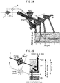
- FIG. 2A and FIG. 2B are diagrams conceptually showing a time / space-resolved measurement method of a photo-excited electron using the time-resolved photoemission electron microscopy 100
- FIG. 2A is a first diagram for explanation
- FIG. 2B is a second diagram for separation.
- a band structure of GaAs is shown and VB indicates a valence band, E F indicates a Fermi level, CB indicates a conduction band, and E VAC indicates a vacuum level.
- a sample such as a GaAs wafer (see FIG. 2A )
- the pump light pulse 8 of 2.4 eV
- an electron located in the valence band is excited to the conduction band.
- the electrons excited to the conduction band by the irradiation of the pump light pulse 8 is emitted from the sample as photoelectrons, by irradiating the sample with the probe light pulse 7.
- the photoelectrons emitted from the sample as photoelectrons are observed by the photoemission electron microscopy.
- the work function ⁇ corresponds to the energy difference between the Fermi level E F and the vacuum level E VAC .
- An electron affinity ⁇ corresponds to the energy difference between the vacuum level E VAC and the conduction band.
- the electron affinity ⁇ is ionization energy.
- symbols 12 indicates images observed at a time interval of 2 ps by the photoemission electron microscopy 6, and a small rectangle on each image corresponds to the irradiation area of the pump light 8 on the GaAs wafer.
- the graph at the bottom right in FIG. 2A is a graph representing a variation over time in the PEEM intensity (PEEM Int.) found from the observation by the photoemission electron microscopy 6.
- the vertical axis in the graph at the bottom left in FIG. 2A represents the PEEM intensity in arbitrary units and the horizontal axis represents a measurement time ⁇ t in ps.
- the inventors, et al. of the present invention have repeatedly performed the experiment to capture images showing the carrier dynamics in insulator and semiconductor materials by using the time-resolved photoemission electron microscopy 100, the influence of charging of the sample is large, and therefore it is not easy to stably capture images with a high S/N ratio.
- the inventors, et al. of the present invention have found a time-resolved photoemission electron microscopy configured to continuously vary the energy of the pump light pulse and the probe light pulse, i.e., the wavelength of the pump light pulse and the probe light pulse.
- the inventors, et al. of the present invention have performed various experiments by using the time-resolved photoemission electron microscopy configured to continuously vary the energy of the pump light pulse and the probe light pulse, and found that unexpected effects as summarized in the following are obtained.
- time-resolved photoemission electron microscopy configured to continuously vary the energy of at least one of the pump light pulse and the probe light pulse is explained in detail.
- FIG. 3 is a block diagram showing an outline configuration of a time-resolved photoemission electron microscopy according to a first embodiment.
- FIG. 3 since the components denoted by the same symbols as those in FIG. 1 indicate the same or similar components of the device in FIG. 1 , duplicated explanation is not given.
- a time-resolved photoemission electron microscopy 101 has the laser light source 1, a pump light generator, a probe light generator, and the photoemission electron microscopy 6.
- the laser light source 1 outputs a pulse having femtosecond level pulse width and variable repetition frequency.
- the pump light generator includes optical elements, such as a nonlinear optical crystal (NL) and lenses, and generates pump light pulse that excites photo-carriers of a sample by converting the wavelength of the light output from the laser light source.
- the probe light generator includes a probe light energy variable device 20 and converts the wavelength of the light output from the laser light source, and generates the probe light pulse that photo-emits photo-carriers excited by the pump light pulse from the sample by the photoelectric effect.
- symbol 20 indicates the probe light energy variable device having a function for varying the energy and wavelength of the probe light pulse 7.
- the probe light energy variable device 20 has an optical mirror 5', a wavelength converter 21, and a high-order harmonic generation device 22 and the optical mirror 5' may be arranged outside the probe light energy variable device 20.
- the wavelength converter 21 is an optical parametric amplifier (OPA) configured to vary, for example, the photon energy of the output light in a range between 0.5 eV and 2.0 eV or a range between 0.5 eV and 2.4 eV.
- OPA optical parametric amplifier
- the energy generated by the wavelength converter 21 depends on the laser light source 1. It is preferable that the probe light energy variable device 20 may continuously vary the energy in a range of ⁇ 3 eV with respect to the ionization energy, the work function, or the electron affinity of the target sample.
- the baseline and the saturation of intensity in the photoelectron emission intensity become clear, since the probe light energy variable device 20 varies the energy continuously in a range of ⁇ 3 eV with respect to the ionization energy, the work function, or the electron affinity of the observation-target sample. Since the baseline and the saturation of intensity in the photoelectron emission intensity become clear, the time-resolved photoemission electron microscope device 101 may observe and measure the energy in a wide energy range.
- the excitation light i.e., the pump light 8 may be selected at three levels of 1.2 eV, 2.4 eV, and 3.6 eV by appropriately select and drive the nonlinear optical crystal (NL) arranged in the pump light generator, in order to widen the range of the target sample.
- the pump light 8 may be selected at the three levels of 1.2 eV, 2.4 eV, and 3.6 eV
- the pump light may be selected discretely at a plurality of arbitrary energies.
- the probe light energy variable device 20 controls the energy of the probe light in a range not less than 3 eV and not more than 5 eV, and it is further preferable that the probe light energy variable device 20 controls the energy of the probe light in a range not less than 0.1 eV and not more than 8 eV. It is preferable that the probe light energy variable device 20 controls the energy of the probe light at an interval of 0.5 eV or less, and it is further preferable that the probe light energy variable device 20 controls the energy of the probe light at an interval of 0.1 eV or less. Further, it is still further preferable that the probe light energy variable device 20 controls the energy of the probe light at an interval of 0.01 eV or less.
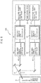
- FIG. 4 is a block diagram showing a detailed configuration of the time-resolved photoemission electron microscopy 101.
- the probe light energy variable device 20 has the wavelength converter 21, which is an OPA, a photon energy selection element stage 23, a first high-order harmonic generation nonlinear crystal stage 24, and a second high-order harmonic generation nonlinear crystal stage 25.
- the photon energy selection element stage 23, the first high-order harmonic generation nonlinear crystal stage 24, and the second high-order harmonic generation nonlinear crystal stage 25 correspond to the high-order harmonic generation device 22.
- Symbol 26 indicates a focus lens stage including a plurality of focus lenses configured to moving in the directions of three axes (X-axis, Y-axis, Z-axis) for accurately focusing the probe light energy-modulated through each of the stages 23, 24, and 24 to the sample position of the photoemission electron microscopy 6.
- the photon energy selection element stage 23 selects a pair of mirrors and a polarizer for selecting energy and polarized light, in accordance with the photon energy generated from the OPA 21.
- the position of the pair of mirrors and a polarizer for selecting energy and polarized light is adjusted by a drive element, such as a motor and a piezo element in the photon energy selection element stage 23.
- the first high-order harmonic generation nonlinear crystal stage 24 adjusts the rotation angle and the position in the vertical and horizontal directions with respect to the optical axis of the nonlinear crystal for generating a high-order harmonic.
- the nonlinear crystal is an element that doubles the energy of a pulse.
- the rotation and position of the nonlinear crystal is adjusted by a drive element, such as a motor and a piezo element for efficiently generating a high-order harmonic (second-order harmonic).
- the second high-order harmonic generation nonlinear crystal stage 25 adjusts the rotation angle and the position in the vertical and horizontal directions with respect to the optical axis of the nonlinear crystal for generating a high-order harmonic.
- the nonlinear crystal is an element that doubles the energy of a pulse.
- the rotation and position of the nonlinear crystal is adjusted by a drive element, such as a motor and a piezo element for efficiently generating a high-order harmonic (second-order harmonic).
- the linear crystal of the second high-order harmonic generation nonlinear crystal stage 25 differs from the linear crystal of the first high-order harmonic generation nonlinear crystal stage 24 in the crystal orientation of cutout.
- a pulse is generated by using both the first high-order harmonic generation nonlinear crystal stage 24 and the second high-order harmonic generation nonlinear crystal stage 25.
- a pulse of 1.5 eV input from the wavelength converter 21 is converted into 3 eV in the first high-order harmonic generation nonlinear crystal stage 24 and converted into 6 eV in the second high-order harmonic generation nonlinear crystal stage 25.
- a pulse of 4 eV is generated in the high-order harmonic generation device 22
- a pulse is generated by using only the first high-order harmonic generation nonlinear crystal stage 24.
- a pulse of 2 eV input from the wavelength converter 21 is converted into 4 eV in the first high-order harmonic generation nonlinear crystal stage 24.
- the 3-axis focus lens stage 26 moves the focus lens in the X-axis direction, the Y-axis direction, and the Z-axis direction in order to keep constant the focusing size and position of the pump light on the surface of the sample i.e., the observation target, wherein the focusing size and position vary by a variation in the energy of the probe light.
- the focus lens is moved by a drive element, such as a motor and a piezo element, by the automatically controlled by a focus lens control device, not shown schematically.
- An optical delay stage 30 corrects a deviation in time between the pump light 8 and the probe light 7.
- a deviation in time between the pump light pulse 8 and the probe light pulse 7 is corrected by a drive element, such as a motor and a piezo element, and the optical delay stage 30 corresponds to the optical delay stage DS shown in FIG. 3 .
- the optical delay stage 30 is inserted into the path in which the probe light pulse is generated, the optical delay stage 30 may be arranged in one of the path in which the pump light is generated and the path in which the probe light is generated.
- FIG. 5 is a block diagram showing an outline configuration of a time-resolved photoemission electron microscopy according to a second embodiment.
- FIG. 5 since the components denoted by the same symbols as those in FIG. 1 indicate the same or similar components as those of the device in FIG. 1 , duplicated explanation is not given.
- symbol 40 indicates a pump light energy variable device having a function for varying the energy and wavelength of the pump light 8.
- the pump light energy variable device 40 has a wavelength converter 41 and a high-order harmonic generation device 42.
- the wavelength converter 41 is the optical parametric amplifier (OPA) configured to vary the photon energy of the output light in a range between 0.5 eV and 2.4 eV, like the wavelength converter 21. It is preferable that the pump light energy variable device 40 may continuously vary the energy in a range of ⁇ 3 eV with respect to the energy of the band gap of the observation-target sample.
- the energy of the band gap, the presence / absence of the impurity level, also referred to as the defect level, and the energy of the impurity level become clear, since the pump light energy variable device 40 varies the energy in a range of ⁇ 3 eV with respect to the energy of the band gap of the target sample.
- the time-resolved photoemission electron microscopy 102 may measure the variation of the band gap in a small area of the sample and the distribution of the impurity level.
- the probe light 7 may be selected at five levels of 1.2 eV, 2.4 eV, 3.6 eV, 4.8 eV, and 6 eV by appropriately select and drive the nonlinear optical crystal (NL) arranged in the probe light generator, in order to widen the range of the target sample.
- NL nonlinear optical crystal
- the probe light 7 may be selected at the five levels of 1.2 eV, 2.4 eV, 3.6 eV, 4.8 eV, and 6 eV
- the pump light may be selected discretely at a plurality of arbitrary energies.
- the pump light energy variable device 40 may continuously vary the energy of the pump light from 0.1 eV up to about 8 eV.
- the band gap of many semiconductors is less than or equal to 5 eV, and even if the band gap is lower, the band gap is about 3 eV.
- the pump light energy variable device 40 may be applied to almost all the target. It is preferable that the pump light energy variable device 40 controls the energy of the probe light in a range not less than 3 eV and not more than 5 eV and it is further preferable that the pump light energy variable device 40 controls the energy of the probe light in a range not less than 0.1 eV and not more than 8 eV.
- the pump light energy variable device 40 controls the energy of the pump light at an interval of 0.5 eV or less, and it is further preferable that that the pump light energy variable device 40 controls the energy of the pump light at an interval of 0.1 eV or less. Further, it is preferable that the pump light energy variable device 40 controls the energy of the pump light at an interval of 0.01 eV or less.
- the high-order harmonic generation device 42 has the same configuration as that of the high-order harmonic generation device 22, detailed explanation is omitted here.
- FIG. 6 is a block diagram showing an outline configuration of a time-resolved photoemission electron microscopy according to a third embodiment.
- the components denoted by the same symbols as those in FIG. 1 indicate the same or similar components of the device in FIG. 1 , and therefore duplicated explanation is not given.
- a time-resolved photoemission electron microscopy 103 has the probe light energy variable device 20 and the pump light energy variable device 40, and both the energies of the probe light 8 and the pump light 7 can be varied continuously. Since the configurations and functions of the probe light energy variable device 20 and the pump light energy variable device 40 are already explained, detailed explanation is omitted here.
- time-resolved photoemission electron microscopy 103 may continuously vary the energy of the probe light pulse 8, the baseline and the saturation of intensity in the photoelectron emission intensity may become clear. Further, since the time-resolved photoemission electron microscopy 103 may continuously vary the energy of the pump light pulse 7, the energy of the band gap, the presence / absence of the impurity level, and the energy of the impurity level may become clear.
- FIG. 7 is a block diagram showing an outline configuration of a time-resolved photoemission electron microscopy according to a fourth embodiment.
- the components denoted by the same symbols as those in FIG. 6 indicate the same or similar components of the device in FIG. 6 , and therefore duplicated explanation is not given.
- a time-resolved photoemission electron microscopy 104 differs from the time-resolved photoemission electron microscopy 103 in having an attosecond pulse laser light source 11 in place of the femtosecond pulse laser light source 1.
- the attosecond pulse laser light source 11 is an attosecond pulse laser light source that outputs a pulse whose pulse width is the attosecond level and whose repetition frequency is variable. Since the attosecond pulse laser light source 11 has the same configuration and function as those of the femtosecond pulse laser light source 1 except in that the pulse width is the attosecond level, detailed explanation is omitted here.
- the wavelength may be easily variable.
- FIG. 8 is a block diagram showing an outline configuration of a time-resolved photoemission electron microscopy according to a fifth embodiment.
- FIG. 8 since the components denoted by the same symbols as those in FIG. 6 indicate the same or similar components of the device in FIG. 6 , duplicated explanation is not given.
- a time-resolved photoemission electron microscopy 105 differs from the time-resolved photoemission electron microscopy 103 in having a femtosecond pulse laser light source 12 and a timing control device 13. Further, the time-resolved photoemission electron microscopy 105 differs from the time-resolved photoemission electron microscopy 103 in not having the optical delay stage DS.
- the femtosecond pulse laser light source 12 has a configuration similar to that of the femtosecond pulse laser light source 1.
- the femtosecond pulse laser light source 1 outputs femtosecond pulse laser light to the pump light energy variable device 40 and the femtosecond pulse laser light source 12 outputs femtosecond pulse laser light to the probe light energy variable device 20.
- the timing control device 13 is, for example, an electronic computer and controls the timing at which each of the femtosecond pulse laser light source 1 and the femtosecond pulse laser light source 12 outputs femtosecond pulse laser light.
- the timing control device 13 controls each of the femtosecond pulse laser light source 1 and the femtosecond pulse laser light source 12 so as to output femtosecond pulse laser light at timing determined in accordance with the life of the carrier photo-excited by the pump light 8.
- the timing of irradiating a sample with the pump light 8 and the probe light 7 may be controlled with a higher accuracy.
- FIG. 9 is a diagram showing a method of estimating the work function of a minute area of a sample by the time-resolved photoemission electron microscopy 101.
- an n-type Si wafer formed by a natural oxide film (SiO 2 ) is used as a sample, and while the energy of the probe light at a step of 40 meV is increased, the pump / probe method is performed and the PEEM image at each step is acquired.
- FIG. 9A is a graph representing how the photoelectron emission intensity (PEEM int.) varies by a variation in the energy of the probe light
- FIG. 9B to FIG. 9F each show the PEEM image when the energy of the probe light is 4.20 eV, 4.90 eV, 5.07 eV, 5.17 eV, and 5.22 eV.
- the graph shown in FIG. 9A is a spectrum obtained by plotting the local intensity (for example, the portion enclosed by a rectangle in FIG. 9B to FIG. 9F ) of the obtained photoemission electron microscopic images for the energy of the probe light.
- the vertical axis in FIG. 9A represents the photoelectron emission intensity (PEEM Int.) in arbitrary units and the horizontal axis represents the energy of the probe light (Probe energy) in eV.
- the energy of the pump light is fixed to 2.4 eV.
- the photoelectron emission intensity (PEEM intensity) from the natural oxide film-attached n-type Si wafer rises suddenly from a point at which the energy of the probe light exceeds about 5 eV.
- the work function in the measurement area of the sample may be estimated from the slope in FIG. 9A .
- the work function estimated from the slope in FIG. 9A is 5.1 eV.
- the images of the PEEM images in FIG. 9B to FIG. 9F the energy of the probe light is vivid in the vicinity of the work function.
- the work function of Si is 5 eV (literature value) as a value when a material is seen macroscopically.
- the work function is different for each position on the sample surface, and the work function may be estimated with the spatial resolution of the photoemission electron microscopy.
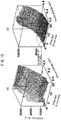
- FIG. 10A and FIG. 10B are each a diagram showing a variation in local photoelectron emission intensity of a sample measured by using an n-type GaAs wafer as a sample and varying the energy of the probe light and the measurement time (delay time, Delay) .
- the energy of the pump light is fixed to 2.4 eV and the exposure time is Is.
- the delay time is varied at a step of 0.2ps and the energy of the probe light (Probe Energy) is varied at a step of 40 meV when the photoelectron emission intensity is measured.
- FIG. 10B is a partially enlarged diagram of FIG. 10A .
- FIG. 11 is a graph representing the relationship between the energy of the probe light and the photoelectron emission intensity when the delay time is fixed to 20 ps and -4 ps, wherein the graph is extracted from the graphs in FIG. 10A and FIG. 10B .
- the vertical axis in FIG.11 represents the local photoelectron emission intensity in the photoemission electron microscopic image in arbitrary units and the horizontal axis represents the energy of the probe light.
- the detected intensity of PEEM rises suddenly after the energy of the probe light reaches 4.4 eV in the curve of -4 ps.
- the local work function of this sample may be estimated to 4.4 eV.
- the curve of 20 ps the photo-excited carrier can be detected by setting energy less than or equal to the measured work function.
- FIG. 12 is a graph extracted from the graph in FIG. 10A and FIG. 10B similar to FIG. 11 , and is a graph representing the relationship between the delay time and the PEEM intensity when the energy of the probe light is set to 4.43 eV and 4.28 eV, which are upper and lower than 4.4 eV of the work function, and 4.43 eV.
- the vertical axis in FIG. 12 represents the local photoelectron emission intensity in a photoemission electron microscopic image in arbitrary units and the horizontal axis represents the delay time in ps.
- the n-type GaAs sample is irradiated with the probe light of 4.43 eV, slightly higher than the work function, no relaxation in the PEEM intensity is observed, and it is understood that the influence of charging of the sample is dominant. Further, the background intensity with the probe light of 4.43 eV is higher than the background intensity the probe light of 4.28 eV. Thus, it is understood that the S/N ratio of the observed image becomes low.
- FIG. 13 is a diagram showing the band structure of n-type GaAs.
- VB indicates a valence band
- CB indicates a conduction band
- Eg indicates a band gap.
- the n-type GaAs has an impurity level under the conduction band.
- the energy difference between the conduction band and the vacuum level is the electron affinity (ionization energy).
- a value slightly lower than the work function for example, a value in the vicinity of the electron affinity (ionization energy) as the energy of the probe light, in order to obtain a vivid photoemission electron microscopic image with a high S/N ratio by emitting only the desired electron, for example, only the photo-excited electron as a photoelectron, and suppressing charging of the sample.
- an electronic computer measures the PEEM intensity by varying the energy of the probe light in a wide range in the time-resolved photoemission electron microscopy 101, in order to obtain a vivid image of the carrier dynamics.
- the computer gives a command to vary continuously the energy of the probe light in a range within ⁇ 3 eV with respect to the electron affinity or the work function of the sample.
- the computer finds the work function of the target area of the sample from the PEEM intensity measured by varying the energy of the probe light.
- the computer finds the local work function of the sample from the energy at which the PEEM intensity rises when the energy of the probe light is varied.
- the computer determines a value in accordance with the found work function as the energy of the probe light.
- the computer selects a plurality of values including a value lower than the found work function and a value higher than the found work function as the energies of the probe light, and observes the PEEM intensity by each energy as time elapses, and then, determines the energy whose influence of charging is estimated to be small as the energy of the probe light when acquiring the PEEM image.
- the computer acquires the PEEM image by the determined energy of the probe light as, for example, shown in FIG. 2A .
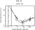
- FIG. 14 is a universal curve indicating a relationship between the photoelectron kinetic energy and the photoelectron escape depth.
- the vertical axis represents the photoelectron escape depth in nm and the horizontal axis represents the photoelectron kinetic energy in eV.
- the escape depth indicates the position in the depth direction of a sample, from which electrons emitted as photoelectrons from the sample comes out. It is known that the relationship between the kinetic energy and the escape depth of electrons emitted as photoelectrons is constant irrespective of material and what indicates this relationship is the universal curve.
- the kinetic energy of electrons emitted as photoelectrons is a value obtained by subtracting the electron affinity (ionization energy) or the work function of the target sample from the energy of the probe light.
- the kinetic energy of electrons emitted as photoelectrons may be controlled by adjusting the energy of the probe light. In other words, the depth at which electrons escapes from the sample may be controlled, by controlling the energy of the probe light.
- the carrier dynamics of electrons located at a depth down to 100 nm from the sample surface it is sufficient to adjust the energy of the probe light so that the kinetic energy of emitted photoelectrons is about 1 eV by referring to FIG. 14 .
- the dynamics of electrons located at a depth of 100 nm or deeper it is sufficient to adjust the energy of the probe light so that the kinetic energy of emitted photoelectrons is about 3.0 eV by referring to FIG. 14 .
- information on the inside (bulk) of an target sample may be selectively detected, by adjusting the energy of the probe light.
Landscapes
- Physics & Mathematics (AREA)
- Analytical Chemistry (AREA)
- Chemical & Material Sciences (AREA)
- General Physics & Mathematics (AREA)
- Biochemistry (AREA)
- Health & Medical Sciences (AREA)
- Life Sciences & Earth Sciences (AREA)
- Nonlinear Science (AREA)
- General Health & Medical Sciences (AREA)
- Immunology (AREA)
- Pathology (AREA)
- Optics & Photonics (AREA)
- Spectroscopy & Molecular Physics (AREA)
- Analysing Materials By The Use Of Radiation (AREA)
Abstract
Description
- The present invention relates to a time-resolved photoemission electron microscopy combining a pump / probe method and photoemission electron microscopy, wherein a femtosecond pulse laser is used as a light source outputting a pulse whose pulse width is less than or equal to a femtosecond level and whose repetition frequency is variable. In more detail, the present invention relates to a time-resolved photoemission electron microscopy configured to observe the behavior of charge carriers (hereinafter, also referred to as carrier dynamics) in a target sample with high sensitivity, and an acquisition method of imaging carrier dynamics by this technique.
- A method has already been proposed that observes the behavior of electrons in a metalic material in accordance with the pump / prove method by using a pulse laser whose repetition frequency and wavelength are fixed as an excitation light source of the photoemission electron microscopy (see Non-patent Literature 1). On the other hand, it is strongly desired to develop a device and method which may directly observe the behavior of electrons in a semiconductor material and an insulator having high resistivity, and not in a metalic material. A femtosecond pulse laser having a temporal width of a femtosecond level may be used in order to implement a high time-resolved resolution i.e., femtosecond scale. Since the sample is charged due to the shortage of electrons by irradiating with a femtosecond pulse laser, it is not easy to create an image of carrier dynamics by an observation device, such as an electron microscope and photoemission electron microscopy.
- The influence of charging of a sample due to irradiation with a femtosecond pulse laser may be reduced by reducing the photon density of the pulse of the femtosecond pulse laser. However, when the photon density of the pulse of the femtosecond pulse laser is reduced, the measurement time may be longer and, the signal-noise ratio (SN ratio) may be reduced.
- In order to solve the above-described problems, the inventors, et al. of the present invention have proposed a time-resolved photoemission electron microscopy combining the pump / probe method and the photoemission electron microscopy, using a repetition frequency variable femtosecond pulse laser as a light source (see Patent Literature 1). Since the photoemission electron microscopy described in
Patent Literature 1 may suppress charging of a sample, the carrier dynamics in a semiconductor may be observed with a high temporal resolution and a high spatial resolution. - [PTL 1] Japanese Unexamined Patent Publication No.
2016-138801 - [NPL 1] A. Kubo et. al., "Femtosecond imaging of surface plasmon dynamics in a nanostructured silver film", NanoLetters, 5 (6), 1123, 2005
- An object of the present invention is to provide a technique configured to acquire a photoelectron image having a high S/N ratio by further improving a time-resolved photoemission electron microscopy combining the pump / probe method and the photoemission electron microscopy and further reducing charging of a sample.
- According to a first aspect of the present invention, in order to attain the above-described object, there is provided a time-resolved photoemission electron microscopy having a laser light source that outputs a pulse having less than or equal to a femtosecond level pulse width and variable repetition frequency, a pump light pulse generator configured to generate pump light pulse that excites the photo-carriers in a sample by converting the wavelength of light pulse output from the laser light source, and a probe light pulse generator configured to generate probe light pulse that photo-emits the photo-excited carriers by the pump light from the sample by the photoelectric effect by converting the wavelength of the light output from the laser light source, and at least the energy of one of the pump light pulse and that of the probe light pulse can be varied continuously.
- In the time-resolved photoemission electron microscopy described above, the probe light pulse generator may be configured to continuously vary the energy of the probe light pulse.
- In the time-resolved photoemission electron microscopy described above, the probe light pulse generator may have an optical parametric amplifier that converts the wavelength of light output from the laser light source.
- Further, the time-resolved photoemission electron microscopy described above may comprise one or more high-order harmonic generation device that generates the probe light pulse from the light source whose wavelength is converted by the optical parametric amplifier.
- Further, in the time-resolved photoemission electron microscopy described above, the variable range of the energy in the probe light pulse generator may be within ±3 eV with respect to the electron affinity or the work function of the target sample.
- Further, the time-resolved photoemission electron microscopy described above may further have a focusing lens stage that keeps constant the focusing position and size of the probe light pulse.
- Further, in the time-resolved photoemission electron microscopy described above, the position of the focus lens maybe moved by drive stages.
- Further, in the time-resolved photoemission electron microscopy described above, the laser light source may have a first laser light source that outputs light to the pump light pulse generator, a second laser light source that outputs light to the probe light pulse generator, and a timing control device that controls timing at which the first laser light source and the second laser light source output light.
- Further, in the time-resolved photoemission electron microscopy described above, the pump light pulse generator may be configured to continuously vary the energy of the pump light pulse.
- According to a second aspect of the present invention, there is provided a method of acquiring a image of photo-excited carrier dynamics by using a time-resolved photoemission electron microscopy that observes photo-carriers excited by the pump light pulse irradiation by irradiating the sample with the probe light pulse by the photoelectric effect, i.e., an acquisition method of a carrier dynamics image by making continuously variable the energy of the probe light in a range within ±3 eV with respect to the electron affinity or the work function of the sample, measuring a photoelectron emission intensity, finding the work function of the observation-target area of the sample from a variation over time in the photoelectron emission intensity, determining the value in accordance with the found work function as the energy of the probe light, and acquiring the carrier dynamics image by the determined probe light energy.
- A photoelectron image having a high S/N ratio may be acquired by further improving a time-resolved photoemission electron microscopy combining a pump / probe method and photoemission electron microscopy and further reducing charging of a sample.
- More specifically, a local (nanoscale) work function of a sample, the energy of a band gap, presence / absence of an impurity level, and energy of the impurity level may be estimated (first effect), by the time-resolved photoemission electron microscopy and the method according to the present invention. Further, an image having a high S/N ratio by reducing the influence of charging of a sample may be acquired (second effect), by the time-resolved photoemission electron microscopy and the method according to the present invention. Furthermore, the escape depth of a carrier from a sample by selecting the kinetic energy of emitted photoelectrons may be controlled (third effect), by the time-resolved photoemission electron microscopy and the method according to the present invention. Still furthermore, sample bulk information may be acquired (by the third effect).
-
-
FIG. 1 is a diagram showing an outline configuration of a conventional time-resolved photoemission electron microscopy using a repetition frequency variable femtosecond pulse laser; -
FIG. 2A and FIG. 2B are diagrams conceptually showing time / space / -resolved measurement by the time-resolved photoemission electron microscopy shown inFIG. 1 andFIG. 2A is a first diagram for explanation andFIG. 2B is a second diagram for explanation; -
FIG. 3 is a diagram showing an outline configuration of a time-resolved photoemission electron microscope device according to a first embodiment; -
FIG. 4 is a block diagram showing a detailed configuration of the time-resolved photoemission electron microscope device shown inFIG. 3 ; -
FIG. 5 is a diagram showing an outline configuration of a time-resolved photoemission electron microscopy according to a second embodiment; -
FIG. 6 is a diagram showing an outline configuration of a time-resolved photoemission electron microscopy according to a third embodiment; -
FIG. 7 is a diagram showing an outline configuration of a time-resolved photoemission electron microscopy according to a fourth embodiment; -
FIG. 8 is a diagram showing an outline configuration of a time-resolved photoemission electron microscopy according to a fifth embodiment; -
FIG. 9A to FIG. 9F are diagrams showing a relationship between the energy of probe light pulse and photoelectron emission intensity obtained by applying the time-resolved photoemission electron microscopy to an n-type Si wafer with an oxide layer shown inFIG. 3 ; -
FIG. 10A and FIG. 10B are diagrams showing a relationship between the energy of probe light pulse, delay time, and photoelectron emission intensity obtained by applying the time-resolved photoemission electron microscopy to an n-type GaAs wafer shown inFIG. 3 ; -
FIG. 11 is a diagram showing a relationship between the energy of probe light pulse and photoelectron emission intensity extracted fromFIG. 10A and FIG. 10B when delay time is fixed; -
FIG. 12 is a diagram showing a relationship between delay time and photoelectron emission intensity extracted fromFIG. 10A and FIG. 10B when the energy of probe light pulse is fixed; -
FIG. 13 is a diagram showing a band structure of n-type GaAs; and -
FIG. 14 is a diagram showing a universal curve. -
FIG. 1 is a diagram showing an outline configuration of the time-resolved photoemission electron microscopy proposed by the inventors, et al. of the present invention inPatent Literature 1. Although the details and the operation principles of the time-resolved photoemission electron microscopy shown inFIG. 1 are described inPatent Literature 1, an outline of the time-resolved photoemission electron microscopy shown inFIG. 1 is described briefly below in order to understand easily the present invention. - In a time-resolved
photoemission electron microscopy 100,symbol 1 indicates a repetition frequency variable femtosecond pulse laser light source whose oscillation wavelength, pulse width, and repetition frequency are 1,028 nm (1.2 eV), 180 fs, and 1 kHz to 1 MHz, respectively.Symbols laser light source 1. A plurality ofsymbols 5 each indicates an optical mirror for converting a light path and focusing light.Symbol 6 indicates photoemission electron microscopy and symbol DS indicates an optical delay stage for delayingprobe light 8 that enters thephotoemission electron microscopy 6. - In the time-resolved
photoemission electron microscopy 100, the laser light generated by the femtosecond pulselaser light source 1 and having a wavelength corresponding to 1.2 eV may be converted into the pump light (excitation light) 8 having a wavelength corresponding to 1.2 eV or 2.4 eV by appropriately selecting and driving the first and second nonlinearoptical crystals optical crystals probe light 7 or may be inserted into the generation path of thepump light 8. - In the time-resolved photoemission electron microscopy shown in
FIG. 1 , a repetition frequency f of the femtosecond pulse laser light output from the femtosecond pulselaser light source 1 is set so that f < 1 / τ holds, wherein the forbidden bandwidth of a sample set within thephotoemission electron microscopy 6 is taken as Eg, the work function as ϕ, and the life of the photo-excited carriers (electron) as τ. Further, energy Ea of thepump light 8 whose wavelength is λa is set so that Ea > Eg holds for the forbidden bandwidth Eg of the sample. Furthermore, energy Eb of the probelight pulse 7 whose wavelength is λb is set so that Eb > ϕ holds for the work function ϕ of the sample. The sample is prevented from charging due to irradiation of the femtosecond pulse laser light, by setting the repetition frequency f of the femtosecond pulse laser light, the energy Ea of thepump light 8, and the energy Eb of the probelight pulse 7 as described above. Since the time-resolvedphotoemission electron microscopy 100 can suppress the charging of a sample due to irradiation of the femtosecond pulse laser light, the carrier dynamics may be observed by photoemission electron microscopy. -
FIG. 2A and FIG. 2B are diagrams conceptually showing a time / space-resolved measurement method of a photo-excited electron using the time-resolvedphotoemission electron microscopy 100,FIG. 2A is a first diagram for explanation andFIG. 2B is a second diagram for separation. InFIG. 2B , a band structure of GaAs is shown and VB indicates a valence band, EF indicates a Fermi level, CB indicates a conduction band, and EVAC indicates a vacuum level. - When a sample, such as a GaAs wafer (see
FIG. 2A ), is irradiated with, for example, the pumplight pulse 8 of 2.4 eV, an electron located in the valence band is excited to the conduction band. Next, the electrons excited to the conduction band by the irradiation of the pumplight pulse 8 is emitted from the sample as photoelectrons, by irradiating the sample with the probelight pulse 7. The photoelectrons emitted from the sample as photoelectrons are observed by the photoemission electron microscopy. - In
FIG. 2B , the work function ϕ corresponds to the energy difference between the Fermi level EF and the vacuum level EVAC. An electron affinity χ corresponds to the energy difference between the vacuum level EVAC and the conduction band. The electron affinity χ is ionization energy. - In
FIG. 2A ,symbols 12 indicates images observed at a time interval of 2 ps by thephotoemission electron microscopy 6, and a small rectangle on each image corresponds to the irradiation area of thepump light 8 on the GaAs wafer. The graph at the bottom right inFIG. 2A is a graph representing a variation over time in the PEEM intensity (PEEM Int.) found from the observation by thephotoemission electron microscopy 6. The vertical axis in the graph at the bottom left inFIG. 2A represents the PEEM intensity in arbitrary units and the horizontal axis represents a measurement time Δt in ps. - The
photoemission electron microscopy 6 may observe the carrier dynamics, when Δt = 0 the intensity of the photoelectron emission shows the peak and the PEEM intensity decreases gradually by energy relaxation and recombination of the carriers, diffusion into the inside of the sample, and the like. On the other hand, when the influence of charging of the sample is large, thephotoemission electron microscopy 6 does not create images of the carrier dynamics, since the decrease in the PEEM intensity does not occur as shown in the graph at the bottom right inFIG. 2A . - Although the inventors, et al. of the present invention have repeatedly performed the experiment to capture images showing the carrier dynamics in insulator and semiconductor materials by using the time-resolved
photoemission electron microscopy 100, the influence of charging of the sample is large, and therefore it is not easy to stably capture images with a high S/N ratio. The inventors, et al. of the present invention have found a time-resolved photoemission electron microscopy configured to continuously vary the energy of the pump light pulse and the probe light pulse, i.e., the wavelength of the pump light pulse and the probe light pulse. The inventors, et al. of the present invention have performed various experiments by using the time-resolved photoemission electron microscopy configured to continuously vary the energy of the pump light pulse and the probe light pulse, and found that unexpected effects as summarized in the following are obtained. -
- (1) Obsevation of workfunction, band gap energy, presence / absence of an impurity level, and impurity level energy of a sample can be estimated in a small area, such as a nanoscale area. Conventionally it was not possible.
- (2) The S/N ratio of a captured image may be significantly improved by reducing charging of a sample due to irradiation of a femtosecond pulse laser.
- (3) Bulk information on a material by sample depth direction-resolved measurement may be obtained by controlling the kinetic energy of emitted photoelectrons.
- In the following, the time-resolved photoemission electron microscopy configured to continuously vary the energy of at least one of the pump light pulse and the probe light pulse is explained in detail.
-
FIG. 3 is a block diagram showing an outline configuration of a time-resolved photoemission electron microscopy according to a first embodiment. InFIG. 3 , since the components denoted by the same symbols as those inFIG. 1 indicate the same or similar components of the device inFIG. 1 , duplicated explanation is not given. - A time-resolved
photoemission electron microscopy 101 has thelaser light source 1, a pump light generator, a probe light generator, and thephotoemission electron microscopy 6. Thelaser light source 1 outputs a pulse having femtosecond level pulse width and variable repetition frequency. The pump light generator includes optical elements, such as a nonlinear optical crystal (NL) and lenses, and generates pump light pulse that excites photo-carriers of a sample by converting the wavelength of the light output from the laser light source. The probe light generator includes a probe lightenergy variable device 20 and converts the wavelength of the light output from the laser light source, and generates the probe light pulse that photo-emits photo-carriers excited by the pump light pulse from the sample by the photoelectric effect. - In the time-resolved
photoemission electron microscopy 101,symbol 20 indicates the probe light energy variable device having a function for varying the energy and wavelength of the probelight pulse 7. The probe lightenergy variable device 20 has an optical mirror 5', awavelength converter 21, and a high-orderharmonic generation device 22 and the optical mirror 5' may be arranged outside the probe lightenergy variable device 20. - The
wavelength converter 21 is an optical parametric amplifier (OPA) configured to vary, for example, the photon energy of the output light in a range between 0.5 eV and 2.0 eV or a range between 0.5 eV and 2.4 eV. The energy generated by thewavelength converter 21 depends on thelaser light source 1. It is preferable that the probe lightenergy variable device 20 may continuously vary the energy in a range of ±3 eV with respect to the ionization energy, the work function, or the electron affinity of the target sample. The baseline and the saturation of intensity in the photoelectron emission intensity become clear, since the probe lightenergy variable device 20 varies the energy continuously in a range of ±3 eV with respect to the ionization energy, the work function, or the electron affinity of the observation-target sample. Since the baseline and the saturation of intensity in the photoelectron emission intensity become clear, the time-resolved photoemissionelectron microscope device 101 may observe and measure the energy in a wide energy range. - Further, in the time-resolved
photoemission electron microscopy 101, the excitation light, i.e., thepump light 8 may be selected at three levels of 1.2 eV, 2.4 eV, and 3.6 eV by appropriately select and drive the nonlinear optical crystal (NL) arranged in the pump light generator, in order to widen the range of the target sample. In the time-resolvedphotoemission electron microscopy 101, although thepump light 8 may be selected at the three levels of 1.2 eV, 2.4 eV, and 3.6 eV, in the time-resolved photoemission electron microscopy according to the embodiment, the pump light may be selected discretely at a plurality of arbitrary energies. - It is preferable that the probe light
energy variable device 20 controls the energy of the probe light in a range not less than 3 eV and not more than 5 eV, and it is further preferable that the probe lightenergy variable device 20 controls the energy of the probe light in a range not less than 0.1 eV and not more than 8 eV. It is preferable that the probe lightenergy variable device 20 controls the energy of the probe light at an interval of 0.5 eV or less, and it is further preferable that the probe lightenergy variable device 20 controls the energy of the probe light at an interval of 0.1 eV or less. Further, it is still further preferable that the probe lightenergy variable device 20 controls the energy of the probe light at an interval of 0.01 eV or less. -
FIG. 4 is a block diagram showing a detailed configuration of the time-resolvedphotoemission electron microscopy 101. In the time-resolvedphotoemission electron microscopy 101, the probe lightenergy variable device 20 has thewavelength converter 21, which is an OPA, a photon energyselection element stage 23, a first high-order harmonic generationnonlinear crystal stage 24, and a second high-order harmonic generationnonlinear crystal stage 25. The photon energyselection element stage 23, the first high-order harmonic generationnonlinear crystal stage 24, and the second high-order harmonic generationnonlinear crystal stage 25 correspond to the high-orderharmonic generation device 22.Symbol 26 indicates a focus lens stage including a plurality of focus lenses configured to moving in the directions of three axes (X-axis, Y-axis, Z-axis) for accurately focusing the probe light energy-modulated through each of thestages photoemission electron microscopy 6. - The photon energy
selection element stage 23 selects a pair of mirrors and a polarizer for selecting energy and polarized light, in accordance with the photon energy generated from theOPA 21. The position of the pair of mirrors and a polarizer for selecting energy and polarized light is adjusted by a drive element, such as a motor and a piezo element in the photon energyselection element stage 23. - The first high-order harmonic generation
nonlinear crystal stage 24 adjusts the rotation angle and the position in the vertical and horizontal directions with respect to the optical axis of the nonlinear crystal for generating a high-order harmonic. The nonlinear crystal is an element that doubles the energy of a pulse. The rotation and position of the nonlinear crystal is adjusted by a drive element, such as a motor and a piezo element for efficiently generating a high-order harmonic (second-order harmonic). - The second high-order harmonic generation
nonlinear crystal stage 25 adjusts the rotation angle and the position in the vertical and horizontal directions with respect to the optical axis of the nonlinear crystal for generating a high-order harmonic. The nonlinear crystal is an element that doubles the energy of a pulse. The rotation and position of the nonlinear crystal is adjusted by a drive element, such as a motor and a piezo element for efficiently generating a high-order harmonic (second-order harmonic). The linear crystal of the second high-order harmonic generationnonlinear crystal stage 25 differs from the linear crystal of the first high-order harmonic generationnonlinear crystal stage 24 in the crystal orientation of cutout. - For example, when a pulse of 6 eV is generated in the high-order
harmonic generation device 22, a pulse is generated by using both the first high-order harmonic generationnonlinear crystal stage 24 and the second high-order harmonic generationnonlinear crystal stage 25. Specifically, a pulse of 1.5 eV input from thewavelength converter 21 is converted into 3 eV in the first high-order harmonic generationnonlinear crystal stage 24 and converted into 6 eV in the second high-order harmonic generationnonlinear crystal stage 25. Further, when a pulse of 4 eV is generated in the high-orderharmonic generation device 22, a pulse is generated by using only the first high-order harmonic generationnonlinear crystal stage 24. Specifically, a pulse of 2 eV input from thewavelength converter 21 is converted into 4 eV in the first high-order harmonic generationnonlinear crystal stage 24. - Further, the 3-axis
focus lens stage 26 moves the focus lens in the X-axis direction, the Y-axis direction, and the Z-axis direction in order to keep constant the focusing size and position of the pump light on the surface of the sample i.e., the observation target, wherein the focusing size and position vary by a variation in the energy of the probe light. The focus lens is moved by a drive element, such as a motor and a piezo element, by the automatically controlled by a focus lens control device, not shown schematically. - An
optical delay stage 30 corrects a deviation in time between thepump light 8 and theprobe light 7. A deviation in time between the pumplight pulse 8 and the probelight pulse 7 is corrected by a drive element, such as a motor and a piezo element, and theoptical delay stage 30 corresponds to the optical delay stage DS shown inFIG. 3 . Although theoptical delay stage 30 is inserted into the path in which the probe light pulse is generated, theoptical delay stage 30 may be arranged in one of the path in which the pump light is generated and the path in which the probe light is generated. -
FIG. 5 is a block diagram showing an outline configuration of a time-resolved photoemission electron microscopy according to a second embodiment. InFIG. 5 , since the components denoted by the same symbols as those inFIG. 1 indicate the same or similar components as those of the device inFIG. 1 , duplicated explanation is not given. - In a time-resolved
photoemission electron microscopy 102,symbol 40 indicates a pump light energy variable device having a function for varying the energy and wavelength of thepump light 8. The pump lightenergy variable device 40 has awavelength converter 41 and a high-orderharmonic generation device 42. - The
wavelength converter 41 is the optical parametric amplifier (OPA) configured to vary the photon energy of the output light in a range between 0.5 eV and 2.4 eV, like thewavelength converter 21. It is preferable that the pump lightenergy variable device 40 may continuously vary the energy in a range of ±3 eV with respect to the energy of the band gap of the observation-target sample. The energy of the band gap, the presence / absence of the impurity level, also referred to as the defect level, and the energy of the impurity level become clear, since the pump lightenergy variable device 40 varies the energy in a range of ±3 eV with respect to the energy of the band gap of the target sample. Since the energy of the band gap, the presence / absence of the impurity level, and the energy of the impurity level become clear, the time-resolvedphotoemission electron microscopy 102 may measure the variation of the band gap in a small area of the sample and the distribution of the impurity level. - Further, in the time-resolved photoemission
electron microscope device 102, theprobe light 7 may be selected at five levels of 1.2 eV, 2.4 eV, 3.6 eV, 4.8 eV, and 6 eV by appropriately select and drive the nonlinear optical crystal (NL) arranged in the probe light generator, in order to widen the range of the target sample. In the time-resolvedphotoemission electron microscopy 102, although theprobe light 7 may be selected at the five levels of 1.2 eV, 2.4 eV, 3.6 eV, 4.8 eV, and 6 eV, in the time-resolved photoemission electron microscopy according to the present embodiment, the pump light may be selected discretely at a plurality of arbitrary energies. - The pump light
energy variable device 40 may continuously vary the energy of the pump light from 0.1 eV up to about 8 eV. The band gap of many semiconductors is less than or equal to 5 eV, and even if the band gap is lower, the band gap is about 3 eV. Thus, the pump lightenergy variable device 40 may be applied to almost all the target. It is preferable that the pump lightenergy variable device 40 controls the energy of the probe light in a range not less than 3 eV and not more than 5 eV and it is further preferable that the pump lightenergy variable device 40 controls the energy of the probe light in a range not less than 0.1 eV and not more than 8 eV. It is preferable that the pump lightenergy variable device 40 controls the energy of the pump light at an interval of 0.5 eV or less, and it is further preferable that that the pump lightenergy variable device 40 controls the energy of the pump light at an interval of 0.1 eV or less. Further, it is preferable that the pump lightenergy variable device 40 controls the energy of the pump light at an interval of 0.01 eV or less. - Since the high-order
harmonic generation device 42 has the same configuration as that of the high-orderharmonic generation device 22, detailed explanation is omitted here. -
FIG. 6 is a block diagram showing an outline configuration of a time-resolved photoemission electron microscopy according to a third embodiment. InFIG. 6 , the components denoted by the same symbols as those inFIG. 1 indicate the same or similar components of the device inFIG. 1 , and therefore duplicated explanation is not given. - A time-resolved
photoemission electron microscopy 103 has the probe lightenergy variable device 20 and the pump lightenergy variable device 40, and both the energies of theprobe light 8 and thepump light 7 can be varied continuously. Since the configurations and functions of the probe lightenergy variable device 20 and the pump lightenergy variable device 40 are already explained, detailed explanation is omitted here. - Since the time-resolved
photoemission electron microscopy 103 may continuously vary the energy of the probelight pulse 8, the baseline and the saturation of intensity in the photoelectron emission intensity may become clear. Further, since the time-resolvedphotoemission electron microscopy 103 may continuously vary the energy of the pumplight pulse 7, the energy of the band gap, the presence / absence of the impurity level, and the energy of the impurity level may become clear. -
FIG. 7 is a block diagram showing an outline configuration of a time-resolved photoemission electron microscopy according to a fourth embodiment. InFIG. 7 , the components denoted by the same symbols as those inFIG. 6 indicate the same or similar components of the device inFIG. 6 , and therefore duplicated explanation is not given. - A time-resolved
photoemission electron microscopy 104 differs from the time-resolvedphotoemission electron microscopy 103 in having an attosecond pulse laser light source 11 in place of the femtosecond pulselaser light source 1. The attosecond pulse laser light source 11 is an attosecond pulse laser light source that outputs a pulse whose pulse width is the attosecond level and whose repetition frequency is variable. Since the attosecond pulse laser light source 11 has the same configuration and function as those of the femtosecond pulselaser light source 1 except in that the pulse width is the attosecond level, detailed explanation is omitted here. - Since the time-resolved
photoemission electron microscopy 103 has the attosecond pulse laser light source 11 in place of the femtosecond pulselaser light source 1, the wavelength may be easily variable. -
FIG. 8 is a block diagram showing an outline configuration of a time-resolved photoemission electron microscopy according to a fifth embodiment. InFIG. 8 , since the components denoted by the same symbols as those inFIG. 6 indicate the same or similar components of the device inFIG. 6 , duplicated explanation is not given. - A time-resolved
photoemission electron microscopy 105 differs from the time-resolvedphotoemission electron microscopy 103 in having a femtosecond pulselaser light source 12 and atiming control device 13. Further, the time-resolvedphotoemission electron microscopy 105 differs from the time-resolvedphotoemission electron microscopy 103 in not having the optical delay stage DS. - The femtosecond pulse
laser light source 12 has a configuration similar to that of the femtosecond pulselaser light source 1. The femtosecond pulselaser light source 1 outputs femtosecond pulse laser light to the pump lightenergy variable device 40 and the femtosecond pulselaser light source 12 outputs femtosecond pulse laser light to the probe lightenergy variable device 20. - The
timing control device 13 is, for example, an electronic computer and controls the timing at which each of the femtosecond pulselaser light source 1 and the femtosecond pulselaser light source 12 outputs femtosecond pulse laser light. Thetiming control device 13 controls each of the femtosecond pulselaser light source 1 and the femtosecond pulselaser light source 12 so as to output femtosecond pulse laser light at timing determined in accordance with the life of the carrier photo-excited by thepump light 8. - Since the time-resolved
photoemission electron microscopy 105 generates thepump light 8 and the provelight 7, respectively, from laser light output from the separate femtosecond pulse laser light sources, the timing of irradiating a sample with thepump light 8 and theprobe light 7 may be controlled with a higher accuracy. - Unexpected effects as described above in the photoelectron emission observation of a sample may be obtained by developing the time-resolved photoemission electron microscopy according to the embodiment.
FIG. 9 is a diagram showing a method of estimating the work function of a minute area of a sample by the time-resolvedphotoemission electron microscopy 101. In the first embodiment, an n-type Si wafer formed by a natural oxide film (SiO2) is used as a sample, and while the energy of the probe light at a step of 40 meV is increased, the pump / probe method is performed and the PEEM image at each step is acquired. -
FIG. 9A is a graph representing how the photoelectron emission intensity (PEEM int.) varies by a variation in the energy of the probe light, andFIG. 9B to FIG. 9F each show the PEEM image when the energy of the probe light is 4.20 eV, 4.90 eV, 5.07 eV, 5.17 eV, and 5.22 eV. The graph shown inFIG. 9A is a spectrum obtained by plotting the local intensity (for example, the portion enclosed by a rectangle inFIG. 9B to FIG. 9F ) of the obtained photoemission electron microscopic images for the energy of the probe light. - The vertical axis in
FIG. 9A represents the photoelectron emission intensity (PEEM Int.) in arbitrary units and the horizontal axis represents the energy of the probe light (Probe energy) in eV. The energy of the pump light is fixed to 2.4 eV. This experiment differs from the measurement method shown inFIG. 2 in that a temporal variation in the photoelectron emission intensity is not detected, i.e., the time-resolved measurement is not performed. - As shown in
FIG. 9A , the photoelectron emission intensity (PEEM intensity) from the natural oxide film-attached n-type Si wafer rises suddenly from a point at which the energy of the probe light exceeds about 5 eV. The work function in the measurement area of the sample may be estimated from the slope inFIG. 9A . The work function estimated from the slope inFIG. 9A is 5.1 eV. As shown the images of the PEEM images inFIG. 9B to FIG. 9F , the energy of the probe light is vivid in the vicinity of the work function. - In general, the work function of Si is 5 eV (literature value) as a value when a material is seen macroscopically. However, according to the device of the present invention, the work function is different for each position on the sample surface, and the work function may be estimated with the spatial resolution of the photoemission electron microscopy.
-
FIG. 10A and FIG. 10B are each a diagram showing a variation in local photoelectron emission intensity of a sample measured by using an n-type GaAs wafer as a sample and varying the energy of the probe light and the measurement time (delay time, Delay) . The energy of the pump light is fixed to 2.4 eV and the exposure time is Is. The delay time is varied at a step of 0.2ps and the energy of the probe light (Probe Energy) is varied at a step of 40 meV when the photoelectron emission intensity is measured.FIG. 10B is a partially enlarged diagram ofFIG. 10A . - When the energy of the probe light exceeds 4.4 eV, a gradual reduction in photoelectron emission intensity is not observed regardless of time passage. It is understood based on the observation that photoelectron emission except for the photoelectron emission of the photo-excited electron by the pump light occurs. Further, since the photoelectron emission continues regardless of time passage, the influence of charging of the sample becomes dominant.
-
FIG. 11 is a graph representing the relationship between the energy of the probe light and the photoelectron emission intensity when the delay time is fixed to 20 ps and -4 ps, wherein the graph is extracted from the graphs inFIG. 10A and FIG. 10B . The vertical axis inFIG.11 represents the local photoelectron emission intensity in the photoemission electron microscopic image in arbitrary units and the horizontal axis represents the energy of the probe light. As shown in the graph, the detected intensity of PEEM rises suddenly after the energy of the probe light reaches 4.4 eV in the curve of -4 ps. Thus, the local work function of this sample may be estimated to 4.4 eV. Further, as shown the curve of 20 ps, the photo-excited carrier can be detected by setting energy less than or equal to the measured work function. -
FIG. 12 is a graph extracted from the graph inFIG. 10A and FIG. 10B similar toFIG. 11 , and is a graph representing the relationship between the delay time and the PEEM intensity when the energy of the probe light is set to 4.43 eV and 4.28 eV, which are upper and lower than 4.4 eV of the work function, and 4.43 eV. The vertical axis inFIG. 12 represents the local photoelectron emission intensity in a photoemission electron microscopic image in arbitrary units and the horizontal axis represents the delay time in ps. - As seen in the graph in
FIG. 12 , when the n-type GaAs sample is irradiated with the probe light having an energy of 4.28 eV, slightly lower than 4.4 eV of the work function, the photoelectron emission intensity decreases gradually from the peak value in accordance with time passage. Thus, it is understood that an image having high S/N ratio is obtained in the observation of the photoelectron emission intensity when the energy of the probe light is set to 4.28 eV. - On the other hand, when the n-type GaAs sample is irradiated with the probe light of 4.43 eV, slightly higher than the work function, no relaxation in the PEEM intensity is observed, and it is understood that the influence of charging of the sample is dominant. Further, the background intensity with the probe light of 4.43 eV is higher than the background intensity the probe light of 4.28 eV. Thus, it is understood that the S/N ratio of the observed image becomes low.
- As above, although the difference is as low as 150 meV with the work function being sandwiched in between, the difference between 4.28 eV and 4.43 eV of the energy of the probe light is large in the observation, and therefore 4.28 eV, which is a value slightly lower than the work function, should be selected as the energy of the probe light in order to obtain a vivid photoemission electron microscopic image for observation of carrier dynamics. The reason is understood as follows.
-
FIG. 13 is a diagram showing the band structure of n-type GaAs. InFIG. 13 , VB indicates a valence band, CB indicates a conduction band, and Eg indicates a band gap. The n-type GaAs has an impurity level under the conduction band. When a sample is irradiated with the probe light of, for example, 4.43 eV, which is an energy slightly higher than the work function of the n-type GaAs, by the irradiation of the pump light, carriers that is located at the impurity level and does not contribute to the dynamic characteristic is emitted as a photoelectron in addition to carriers excited from the valence band to the conduction band, and it is understood that carriers located at the impurity level increase the background in the photoelectron emission intensity and reduce the S/N ratio by inducing charging of the sample. - On the other hand, when the sample is irradiated with the probe light whose energy is an energy slightly lower than the work function of the n-type GaAs, for example, 4.28 eV, carriers at the impurity level is not emitted as a photoelectron and only carriers excited from the valence band to the conduction band by the pump light is emitted as a photoelectron. Thus, charging of the sample is reduced and the photoelectron emission intensity in accordance with time passage is observed with a high S/N ratio.
- The energy difference between the conduction band and the vacuum level is the electron affinity (ionization energy). Thus, it is preferable to select a value slightly lower than the work function, for example, a value in the vicinity of the electron affinity (ionization energy) as the energy of the probe light, in order to obtain a vivid photoemission electron microscopic image with a high S/N ratio by emitting only the desired electron, for example, only the photo-excited electron as a photoelectron, and suppressing charging of the sample.
- Based on the results of the third embodiment, an electronic computer, not shown schematically, measures the PEEM intensity by varying the energy of the probe light in a wide range in the time-resolved
photoemission electron microscopy 101, in order to obtain a vivid image of the carrier dynamics. For example, the computer gives a command to vary continuously the energy of the probe light in a range within ±3 eV with respect to the electron affinity or the work function of the sample. Next, the computer finds the work function of the target area of the sample from the PEEM intensity measured by varying the energy of the probe light. The computer finds the local work function of the sample from the energy at which the PEEM intensity rises when the energy of the probe light is varied. Next, the computer determines a value in accordance with the found work function as the energy of the probe light. The computer selects a plurality of values including a value lower than the found work function and a value higher than the found work function as the energies of the probe light, and observes the PEEM intensity by each energy as time elapses, and then, determines the energy whose influence of charging is estimated to be small as the energy of the probe light when acquiring the PEEM image. Then, the computer acquires the PEEM image by the determined energy of the probe light as, for example, shown inFIG. 2A . -
FIG. 14 is a universal curve indicating a relationship between the photoelectron kinetic energy and the photoelectron escape depth. InFIG. 14 , the vertical axis represents the photoelectron escape depth in nm and the horizontal axis represents the photoelectron kinetic energy in eV. The escape depth indicates the position in the depth direction of a sample, from which electrons emitted as photoelectrons from the sample comes out. It is known that the relationship between the kinetic energy and the escape depth of electrons emitted as photoelectrons is constant irrespective of material and what indicates this relationship is the universal curve. - The kinetic energy of electrons emitted as photoelectrons is a value obtained by subtracting the electron affinity (ionization energy) or the work function of the target sample from the energy of the probe light. Thus, the kinetic energy of electrons emitted as photoelectrons may be controlled by adjusting the energy of the probe light. In other words, the depth at which electrons escapes from the sample may be controlled, by controlling the energy of the probe light.
- For example, when the carrier dynamics of electrons located at a depth down to 100 nm from the sample surface is measured, it is sufficient to adjust the energy of the probe light so that the kinetic energy of emitted photoelectrons is about 1 eV by referring to
FIG. 14 . Further, when the dynamics of electrons located at a depth of 100 nm or deeper is measured, it is sufficient to adjust the energy of the probe light so that the kinetic energy of emitted photoelectrons is about 3.0 eV by referring toFIG. 14 . - As above, information on the inside (bulk) of an target sample may be selectively detected, by adjusting the energy of the probe light.
Claims (10)
- A time-resolved photoemission electron microscopy comprising:a laser light source that outputs a pulse having less than or equal to a femtosecond level pulse width and variable repetition frequency;a pump light pulse generator configured to generate pump light pulse that excites photo-carriers of a sample by converting wavelength of light output from the laser light source; anda probe light pulse generator configured to generate probe light pulse that photo-emits photo-carriers excited by the pump light pulse from the sample by photoelectric effect by converting wavelength of light output from the laser light source, whereinenergy of at least one of the pump light pulse and the probe light pulse is configured to continuously vary.
- The time-resolved photoemission electron microscopy according to claim 1, wherein
the probe light pulse generator is configured to continuously vary energy of the probe light pulse. - The time-resolved photoemission electron microscopy according to claim 2, wherein
the probe light pulse generator has an optical parametric amplifier that converts wavelength of light output from the laser light source. - The time-resolved photoemission electron microscopy according to claim 2, wherein
the probe light pulse generator further has a high-order harmonic generation device that generates the probe light pulse from light whose wavelength is converted by an optical parametric amplifier. - The time-resolved photoemission electron microscopy according to any one of claims 2 to 4, wherein
a range in which the probe light pulse generator is configured to vary energy is within ±3 eV with respect to an electron affinity, ionization energy, or work function of an target sample. - The time-resolved photoemission electron microscopy according to any one of claims 2 to 5, further comprising:
a focus lens stage that keeps constant a focus position and a size of the probe light. - The time-resolved photoemission electron microscopy according to claim 6, wherein
the focus lens stage has a focus lens and a drive element that moves a position of the focus lens. - The time-resolved photoemission electron microscopy according to any one of claims 1 to 7, wherein
the pump light pulse generator is configured to continuously vary energy of the pump light pulse. - The time-resolved photoemission electron microscopy according to any one of claims 2 to 8, wherein
the laser light source has a first laser light source that outputs light to the pump light pulse generator, a second laser light source that outputs light to the probe light pulse generator, and a timing control device that controls timing at which the first laser light source and the second laser light source output light. - A method of acquiring a photo-excited carrier dynamics image by using a time-resolved photoemission electron microscopy that observes photo-carriers emitted from a sample by irradiating the sample with pump light pulse to excite the photo-carriers of the sample and irradiating the sample with probe light pulse to photo-emit the photo-carriers excited by the pump light pulse from the sample by photoelectric effect, comprising steps of:varying continuously energy of the probe light pulse in a range within ±3 eV with respect to an electron affinity or work function of the sample;measuring photoelectron emission intensity;finding the work function of a target area of the sample from a variation over time in the photoelectron emission intensity;determining a value in accordance with the found work function as the energy of the probe light; andacquiring the carrier dynamics image by the determined probe light energy.
Applications Claiming Priority (2)
| Application Number | Priority Date | Filing Date | Title |
|---|---|---|---|
| JP2017037139 | 2017-02-28 | ||
| PCT/JP2018/004734 WO2018159272A1 (en) | 2017-02-28 | 2018-02-09 | Time-resolved photoemission electron microscope device and method for acquiring carrier dynamics image using said device |
Publications (3)
| Publication Number | Publication Date |
|---|---|
| EP3591388A1 true EP3591388A1 (en) | 2020-01-08 |
| EP3591388A4 EP3591388A4 (en) | 2021-03-31 |
| EP3591388B1 EP3591388B1 (en) | 2022-05-11 |
Family
ID=63370073
Family Applications (1)
| Application Number | Title | Priority Date | Filing Date |
|---|---|---|---|
| EP18760545.6A Active EP3591388B1 (en) | 2017-02-28 | 2018-02-09 | Time-resolved photoemission electron microscope device and method for acquiring carrier dynamics image using said device |
Country Status (4)
| Country | Link |
|---|---|
| US (1) | US10989679B2 (en) |
| EP (1) | EP3591388B1 (en) |
| JP (1) | JP7072805B2 (en) |
| WO (1) | WO2018159272A1 (en) |
Cited By (1)
| Publication number | Priority date | Publication date | Assignee | Title |
|---|---|---|---|---|
| CN113008840A (en) * | 2021-02-22 | 2021-06-22 | 西北核技术研究所 | Laser pumping detection-based scintillation material transient process characterization system and method |
Families Citing this family (8)
| Publication number | Priority date | Publication date | Assignee | Title |
|---|---|---|---|---|
| JP7354669B2 (en) * | 2018-08-31 | 2023-10-03 | Dic株式会社 | display device |
| WO2020246438A1 (en) * | 2019-06-03 | 2020-12-10 | 国立大学法人東京大学 | Laser light source and photoelectron microscope |
| JP6832592B1 (en) * | 2019-10-21 | 2021-02-24 | 大学共同利用機関法人 高エネルギー加速器研究機構 | Time-resolved photoemission electron microscope device, hole space distribution detection method, hole lifetime estimation method and hole mobility calculation method |
| KR102402681B1 (en) | 2020-04-17 | 2022-05-26 | 한국과학기술원 | Multi photon microscopy, imaging method using time-gated detection thereof |
| CN114544688B (en) * | 2020-11-25 | 2024-07-23 | 中国科学院大连化学物理研究所 | Time resolution angle resolution ultraviolet light electron energy spectrum device based on higher harmonic generation |
| DE102021117409A1 (en) * | 2021-07-06 | 2023-01-12 | Sri Ranjini Arumugam | Method and device for the spatially resolved localization of defects in materials |
| CN115112578B (en) * | 2022-07-19 | 2025-08-12 | 国家纳米科学中心 | Imaging spectrum system based on pump detection, detection imaging method and application |
| CN116642882B (en) * | 2023-04-20 | 2024-02-20 | 之江实验室 | An interference scattering pump detection imaging method and system based on pulse modulation |
Family Cites Families (13)
| Publication number | Priority date | Publication date | Assignee | Title |
|---|---|---|---|---|
| CH493934A (en) * | 1969-04-28 | 1970-07-15 | Balzers Patent Beteilig Ag | Electron emission microscope |
| JP2002168814A (en) * | 2000-11-29 | 2002-06-14 | Hitachi Ltd | Detection device and device evaluation device |
| JP2003066338A (en) * | 2001-08-28 | 2003-03-05 | Olympus Optical Co Ltd | microscope |
| WO2005098895A2 (en) * | 2004-04-02 | 2005-10-20 | California Institute Of Technology | Method and system for ultrafast photoelectron microscope |
| JP2007193230A (en) * | 2006-01-20 | 2007-08-02 | Sumitomo Electric Ind Ltd | Light source device |
| JP4839481B2 (en) * | 2006-11-29 | 2011-12-21 | 独立行政法人科学技術振興機構 | Pump probe measuring apparatus and scanning probe microscope apparatus using the same |
| US8085406B2 (en) * | 2007-08-31 | 2011-12-27 | University Of Pittsburgh Of The Commonwealth System Of Higher Education | Ultrafast microscopy of surface electromagnetic fields |
| US20120293791A1 (en) * | 2008-10-20 | 2012-11-22 | Brookhaven Science Associates, Llc | Sample Holder with Optical Features for Holding a Sample in an Analytical Device for Research Purposes |
| JP5339364B2 (en) * | 2009-07-27 | 2013-11-13 | 独立行政法人理化学研究所 | Laser synchronization method, laser system and pump / probe measurement system |
| KR102609862B1 (en) * | 2014-04-17 | 2023-12-04 | 펨토매트릭스, 인코포레이티드. | Wafer metrology technologies |
| JP2016138801A (en) * | 2015-01-27 | 2016-08-04 | 国立大学法人東京工業大学 | Time-resolved photoemission electron microscope device |
| CN113056814B (en) * | 2018-04-27 | 2025-05-27 | 菲拓梅里克斯公司 | System and method for determining semiconductor device characteristics |
| EP3794335B1 (en) * | 2018-05-15 | 2025-02-19 | Femtometrix, Inc. | Second harmonic generation (shg) optical inspection system designs |
-
2018
- 2018-02-09 JP JP2019502851A patent/JP7072805B2/en active Active
- 2018-02-09 EP EP18760545.6A patent/EP3591388B1/en active Active
- 2018-02-09 US US16/489,522 patent/US10989679B2/en active Active
- 2018-02-09 WO PCT/JP2018/004734 patent/WO2018159272A1/en not_active Ceased
Cited By (2)
| Publication number | Priority date | Publication date | Assignee | Title |
|---|---|---|---|---|
| CN113008840A (en) * | 2021-02-22 | 2021-06-22 | 西北核技术研究所 | Laser pumping detection-based scintillation material transient process characterization system and method |
| CN113008840B (en) * | 2021-02-22 | 2023-01-17 | 西北核技术研究所 | System and method for characterization of transient process of scintillation materials based on laser pump detection |
Also Published As
| Publication number | Publication date |
|---|---|
| US10989679B2 (en) | 2021-04-27 |
| US20200072771A1 (en) | 2020-03-05 |
| EP3591388A4 (en) | 2021-03-31 |
| EP3591388B1 (en) | 2022-05-11 |
| JP7072805B2 (en) | 2022-05-23 |
| WO2018159272A1 (en) | 2018-09-07 |
| JPWO2018159272A1 (en) | 2020-02-06 |
Similar Documents
| Publication | Publication Date | Title |
|---|---|---|
| EP3591388B1 (en) | Time-resolved photoemission electron microscope device and method for acquiring carrier dynamics image using said device | |
| US8669512B2 (en) | System and method for analyzing light by three-photon counting | |
| JP6998469B2 (en) | Electron beam device | |
| US8429761B2 (en) | Photon induced near field electron microscope and biological imaging system | |
| US9978559B2 (en) | Method and device for time-resolved pump-probe electron microscopy | |
| JP6527872B2 (en) | Non-invasive charged particle beam monitor | |
| CN114678244B (en) | Ultrafast scanning electron microscope system and application method thereof | |
| US20240363306A1 (en) | Charged particle beam device | |
| KR20210027064A (en) | Charged particle beam apparatus | |
| JP2016138801A (en) | Time-resolved photoemission electron microscope device | |
| Chew et al. | Imaging Localized Surface Plasmons by Femtosecond to Attosecond Time‐Resolved Photoelectron Emission Microscopy–“ATTO‐PEEM” | |
| US20190348255A1 (en) | Scanning electron microscope and sample observation method using scanning electron microscope | |
| CN114252653B (en) | Ultrafast imaging device and method thereof | |
| Winchester et al. | Methodology and implementation of a tunable deep-ultraviolet laser source for photoemission electron microscopy | |
| TW201946083A (en) | System and method for photocathode illumination inspection | |
| WO2022091234A1 (en) | Charged particle beam device and sample observation method | |
| EP0506397A2 (en) | Optical waveform measuring device | |
| JP6637306B2 (en) | Analysis method and spectrometer | |
| Alvelid | Investigation of the photophysical properties of quantum dots for super-resolution imaging | |
| JP2017091616A (en) | Apparatus and method for measuring energy electron has | |
| TWI888844B (en) | Sample measuring device | |
| KR102965114B1 (en) | Charged particle beam device and sample observation method | |
| Staněk et al. | Photoelectric charge from metallic filters: An online XUV pulse energy diagnostics | |
| Anchugov et al. | Calibration of an image-tube picosecond dissector | |
| Allison | Ultrafast Dynamics of Molecules on Surfaces Studied with Time-Resolved XUV Photoelectron Spectroscopy |
Legal Events
| Date | Code | Title | Description |
|---|---|---|---|
| STAA | Information on the status of an ep patent application or granted ep patent |
Free format text: STATUS: THE INTERNATIONAL PUBLICATION HAS BEEN MADE |
|
| PUAI | Public reference made under article 153(3) epc to a published international application that has entered the european phase |
Free format text: ORIGINAL CODE: 0009012 |
|
| STAA | Information on the status of an ep patent application or granted ep patent |
Free format text: STATUS: REQUEST FOR EXAMINATION WAS MADE |
|
| 17P | Request for examination filed |
Effective date: 20190912 |
|
| AK | Designated contracting states |
Kind code of ref document: A1 Designated state(s): AL AT BE BG CH CY CZ DE DK EE ES FI FR GB GR HR HU IE IS IT LI LT LU LV MC MK MT NL NO PL PT RO RS SE SI SK SM TR |
|
| AX | Request for extension of the european patent |
Extension state: BA ME |
|
| DAV | Request for validation of the european patent (deleted) | ||
| DAX | Request for extension of the european patent (deleted) | ||
| A4 | Supplementary search report drawn up and despatched |
Effective date: 20210226 |
|
| RIC1 | Information provided on ipc code assigned before grant |
Ipc: G01N 23/227 20180101AFI20210222BHEP Ipc: H01J 37/26 20060101ALI20210222BHEP |
|
| GRAP | Despatch of communication of intention to grant a patent |
Free format text: ORIGINAL CODE: EPIDOSNIGR1 |
|
| STAA | Information on the status of an ep patent application or granted ep patent |
Free format text: STATUS: GRANT OF PATENT IS INTENDED |
|
| INTG | Intention to grant announced |
Effective date: 20211208 |
|
| GRAS | Grant fee paid |
Free format text: ORIGINAL CODE: EPIDOSNIGR3 |
|
| GRAA | (expected) grant |
Free format text: ORIGINAL CODE: 0009210 |
|
| STAA | Information on the status of an ep patent application or granted ep patent |
Free format text: STATUS: THE PATENT HAS BEEN GRANTED |
|
| AK | Designated contracting states |
Kind code of ref document: B1 Designated state(s): AL AT BE BG CH CY CZ DE DK EE ES FI FR GB GR HR HU IE IS IT LI LT LU LV MC MK MT NL NO PL PT RO RS SE SI SK SM TR |
|
| REG | Reference to a national code |
Ref country code: GB Ref legal event code: FG4D |
|
| REG | Reference to a national code |
Ref country code: CH Ref legal event code: EP |
|
| REG | Reference to a national code |
Ref country code: AT Ref legal event code: REF Ref document number: 1491832 Country of ref document: AT Kind code of ref document: T Effective date: 20220515 |
|
| REG | Reference to a national code |
Ref country code: DE Ref legal event code: R096 Ref document number: 602018035473 Country of ref document: DE |
|
| REG | Reference to a national code |
Ref country code: IE Ref legal event code: FG4D |
|
| REG | Reference to a national code |
Ref country code: LT Ref legal event code: MG9D |
|
| REG | Reference to a national code |
Ref country code: NL Ref legal event code: MP Effective date: 20220511 |
|
| REG | Reference to a national code |
Ref country code: AT Ref legal event code: MK05 Ref document number: 1491832 Country of ref document: AT Kind code of ref document: T Effective date: 20220511 |
|
| PG25 | Lapsed in a contracting state [announced via postgrant information from national office to epo] |
Ref country code: SE Free format text: LAPSE BECAUSE OF FAILURE TO SUBMIT A TRANSLATION OF THE DESCRIPTION OR TO PAY THE FEE WITHIN THE PRESCRIBED TIME-LIMIT Effective date: 20220511 Ref country code: PT Free format text: LAPSE BECAUSE OF FAILURE TO SUBMIT A TRANSLATION OF THE DESCRIPTION OR TO PAY THE FEE WITHIN THE PRESCRIBED TIME-LIMIT Effective date: 20220912 Ref country code: NO Free format text: LAPSE BECAUSE OF FAILURE TO SUBMIT A TRANSLATION OF THE DESCRIPTION OR TO PAY THE FEE WITHIN THE PRESCRIBED TIME-LIMIT Effective date: 20220811 Ref country code: NL Free format text: LAPSE BECAUSE OF FAILURE TO SUBMIT A TRANSLATION OF THE DESCRIPTION OR TO PAY THE FEE WITHIN THE PRESCRIBED TIME-LIMIT Effective date: 20220511 Ref country code: LT Free format text: LAPSE BECAUSE OF FAILURE TO SUBMIT A TRANSLATION OF THE DESCRIPTION OR TO PAY THE FEE WITHIN THE PRESCRIBED TIME-LIMIT Effective date: 20220511 Ref country code: HR Free format text: LAPSE BECAUSE OF FAILURE TO SUBMIT A TRANSLATION OF THE DESCRIPTION OR TO PAY THE FEE WITHIN THE PRESCRIBED TIME-LIMIT Effective date: 20220511 Ref country code: GR Free format text: LAPSE BECAUSE OF FAILURE TO SUBMIT A TRANSLATION OF THE DESCRIPTION OR TO PAY THE FEE WITHIN THE PRESCRIBED TIME-LIMIT Effective date: 20220812 Ref country code: FI Free format text: LAPSE BECAUSE OF FAILURE TO SUBMIT A TRANSLATION OF THE DESCRIPTION OR TO PAY THE FEE WITHIN THE PRESCRIBED TIME-LIMIT Effective date: 20220511 Ref country code: ES Free format text: LAPSE BECAUSE OF FAILURE TO SUBMIT A TRANSLATION OF THE DESCRIPTION OR TO PAY THE FEE WITHIN THE PRESCRIBED TIME-LIMIT Effective date: 20220511 Ref country code: BG Free format text: LAPSE BECAUSE OF FAILURE TO SUBMIT A TRANSLATION OF THE DESCRIPTION OR TO PAY THE FEE WITHIN THE PRESCRIBED TIME-LIMIT Effective date: 20220811 Ref country code: AT Free format text: LAPSE BECAUSE OF FAILURE TO SUBMIT A TRANSLATION OF THE DESCRIPTION OR TO PAY THE FEE WITHIN THE PRESCRIBED TIME-LIMIT Effective date: 20220511 |
|
| PG25 | Lapsed in a contracting state [announced via postgrant information from national office to epo] |
Ref country code: RS Free format text: LAPSE BECAUSE OF FAILURE TO SUBMIT A TRANSLATION OF THE DESCRIPTION OR TO PAY THE FEE WITHIN THE PRESCRIBED TIME-LIMIT Effective date: 20220511 Ref country code: PL Free format text: LAPSE BECAUSE OF FAILURE TO SUBMIT A TRANSLATION OF THE DESCRIPTION OR TO PAY THE FEE WITHIN THE PRESCRIBED TIME-LIMIT Effective date: 20220511 Ref country code: LV Free format text: LAPSE BECAUSE OF FAILURE TO SUBMIT A TRANSLATION OF THE DESCRIPTION OR TO PAY THE FEE WITHIN THE PRESCRIBED TIME-LIMIT Effective date: 20220511 Ref country code: IS Free format text: LAPSE BECAUSE OF FAILURE TO SUBMIT A TRANSLATION OF THE DESCRIPTION OR TO PAY THE FEE WITHIN THE PRESCRIBED TIME-LIMIT Effective date: 20220911 |
|
| PG25 | Lapsed in a contracting state [announced via postgrant information from national office to epo] |
Ref country code: SM Free format text: LAPSE BECAUSE OF FAILURE TO SUBMIT A TRANSLATION OF THE DESCRIPTION OR TO PAY THE FEE WITHIN THE PRESCRIBED TIME-LIMIT Effective date: 20220511 Ref country code: SK Free format text: LAPSE BECAUSE OF FAILURE TO SUBMIT A TRANSLATION OF THE DESCRIPTION OR TO PAY THE FEE WITHIN THE PRESCRIBED TIME-LIMIT Effective date: 20220511 Ref country code: RO Free format text: LAPSE BECAUSE OF FAILURE TO SUBMIT A TRANSLATION OF THE DESCRIPTION OR TO PAY THE FEE WITHIN THE PRESCRIBED TIME-LIMIT Effective date: 20220511 Ref country code: EE Free format text: LAPSE BECAUSE OF FAILURE TO SUBMIT A TRANSLATION OF THE DESCRIPTION OR TO PAY THE FEE WITHIN THE PRESCRIBED TIME-LIMIT Effective date: 20220511 Ref country code: DK Free format text: LAPSE BECAUSE OF FAILURE TO SUBMIT A TRANSLATION OF THE DESCRIPTION OR TO PAY THE FEE WITHIN THE PRESCRIBED TIME-LIMIT Effective date: 20220511 Ref country code: CZ Free format text: LAPSE BECAUSE OF FAILURE TO SUBMIT A TRANSLATION OF THE DESCRIPTION OR TO PAY THE FEE WITHIN THE PRESCRIBED TIME-LIMIT Effective date: 20220511 |
|
| REG | Reference to a national code |
Ref country code: DE Ref legal event code: R097 Ref document number: 602018035473 Country of ref document: DE |
|
| PLBE | No opposition filed within time limit |
Free format text: ORIGINAL CODE: 0009261 |
|
| STAA | Information on the status of an ep patent application or granted ep patent |
Free format text: STATUS: NO OPPOSITION FILED WITHIN TIME LIMIT |
|
| PG25 | Lapsed in a contracting state [announced via postgrant information from national office to epo] |
Ref country code: AL Free format text: LAPSE BECAUSE OF FAILURE TO SUBMIT A TRANSLATION OF THE DESCRIPTION OR TO PAY THE FEE WITHIN THE PRESCRIBED TIME-LIMIT Effective date: 20220511 |
|
| 26N | No opposition filed |
Effective date: 20230214 |
|
| PG25 | Lapsed in a contracting state [announced via postgrant information from national office to epo] |
Ref country code: SI Free format text: LAPSE BECAUSE OF FAILURE TO SUBMIT A TRANSLATION OF THE DESCRIPTION OR TO PAY THE FEE WITHIN THE PRESCRIBED TIME-LIMIT Effective date: 20220511 |
|
| PG25 | Lapsed in a contracting state [announced via postgrant information from national office to epo] |
Ref country code: MC Free format text: LAPSE BECAUSE OF FAILURE TO SUBMIT A TRANSLATION OF THE DESCRIPTION OR TO PAY THE FEE WITHIN THE PRESCRIBED TIME-LIMIT Effective date: 20220511 |
|
| REG | Reference to a national code |
Ref country code: CH Ref legal event code: PL |
|
| REG | Reference to a national code |
Ref country code: BE Ref legal event code: MM Effective date: 20230228 |
|
| GBPC | Gb: european patent ceased through non-payment of renewal fee |
Effective date: 20230209 |
|
| PG25 | Lapsed in a contracting state [announced via postgrant information from national office to epo] |
Ref country code: LU Free format text: LAPSE BECAUSE OF NON-PAYMENT OF DUE FEES Effective date: 20230209 Ref country code: LI Free format text: LAPSE BECAUSE OF NON-PAYMENT OF DUE FEES Effective date: 20230228 Ref country code: CH Free format text: LAPSE BECAUSE OF NON-PAYMENT OF DUE FEES Effective date: 20230228 |
|
| REG | Reference to a national code |
Ref country code: IE Ref legal event code: MM4A |
|
| PG25 | Lapsed in a contracting state [announced via postgrant information from national office to epo] |
Ref country code: GB Free format text: LAPSE BECAUSE OF NON-PAYMENT OF DUE FEES Effective date: 20230209 |
|
| PG25 | Lapsed in a contracting state [announced via postgrant information from national office to epo] |
Ref country code: IT Free format text: LAPSE BECAUSE OF FAILURE TO SUBMIT A TRANSLATION OF THE DESCRIPTION OR TO PAY THE FEE WITHIN THE PRESCRIBED TIME-LIMIT Effective date: 20220511 Ref country code: IE Free format text: LAPSE BECAUSE OF NON-PAYMENT OF DUE FEES Effective date: 20230209 Ref country code: GB Free format text: LAPSE BECAUSE OF NON-PAYMENT OF DUE FEES Effective date: 20230209 Ref country code: FR Free format text: LAPSE BECAUSE OF NON-PAYMENT OF DUE FEES Effective date: 20230228 |
|
| PG25 | Lapsed in a contracting state [announced via postgrant information from national office to epo] |
Ref country code: BE Free format text: LAPSE BECAUSE OF NON-PAYMENT OF DUE FEES Effective date: 20230228 |
|
| PG25 | Lapsed in a contracting state [announced via postgrant information from national office to epo] |
Ref country code: BG Free format text: LAPSE BECAUSE OF FAILURE TO SUBMIT A TRANSLATION OF THE DESCRIPTION OR TO PAY THE FEE WITHIN THE PRESCRIBED TIME-LIMIT Effective date: 20220511 |
|
| PG25 | Lapsed in a contracting state [announced via postgrant information from national office to epo] |
Ref country code: BG Free format text: LAPSE BECAUSE OF FAILURE TO SUBMIT A TRANSLATION OF THE DESCRIPTION OR TO PAY THE FEE WITHIN THE PRESCRIBED TIME-LIMIT Effective date: 20220511 |
|
| PG25 | Lapsed in a contracting state [announced via postgrant information from national office to epo] |
Ref country code: CY Free format text: LAPSE BECAUSE OF FAILURE TO SUBMIT A TRANSLATION OF THE DESCRIPTION OR TO PAY THE FEE WITHIN THE PRESCRIBED TIME-LIMIT; INVALID AB INITIO Effective date: 20180209 |
|
| PG25 | Lapsed in a contracting state [announced via postgrant information from national office to epo] |
Ref country code: HU Free format text: LAPSE BECAUSE OF FAILURE TO SUBMIT A TRANSLATION OF THE DESCRIPTION OR TO PAY THE FEE WITHIN THE PRESCRIBED TIME-LIMIT; INVALID AB INITIO Effective date: 20180209 |
|
| PG25 | Lapsed in a contracting state [announced via postgrant information from national office to epo] |
Ref country code: TR Free format text: LAPSE BECAUSE OF FAILURE TO SUBMIT A TRANSLATION OF THE DESCRIPTION OR TO PAY THE FEE WITHIN THE PRESCRIBED TIME-LIMIT Effective date: 20220511 |
|
| PGFP | Annual fee paid to national office [announced via postgrant information from national office to epo] |
Ref country code: DE Payment date: 20260217 Year of fee payment: 9 |