EP3591356A1 - Light detector - Google Patents
Light detector Download PDFInfo
- Publication number
- EP3591356A1 EP3591356A1 EP18761748.5A EP18761748A EP3591356A1 EP 3591356 A1 EP3591356 A1 EP 3591356A1 EP 18761748 A EP18761748 A EP 18761748A EP 3591356 A1 EP3591356 A1 EP 3591356A1
- Authority
- EP
- European Patent Office
- Prior art keywords
- support substrate
- light
- viewed
- thickness direction
- layer
- Prior art date
- Legal status (The legal status is an assumption and is not a legal conclusion. Google has not performed a legal analysis and makes no representation as to the accuracy of the status listed.)
- Withdrawn
Links
- 239000000758 substrate Substances 0.000 claims abstract description 272
- 230000005540 biological transmission Effects 0.000 claims abstract description 108
- 230000002787 reinforcement Effects 0.000 claims abstract description 95
- 229910000679 solder Inorganic materials 0.000 claims abstract description 56
- 238000001514 detection method Methods 0.000 claims abstract description 46
- 230000004308 accommodation Effects 0.000 claims abstract description 45
- 239000000463 material Substances 0.000 claims abstract description 27
- 239000011159 matrix material Substances 0.000 claims description 5
- 230000031070 response to heat Effects 0.000 claims description 3
- 239000010410 layer Substances 0.000 description 259
- 230000031700 light absorption Effects 0.000 description 34
- 229910052718 tin Inorganic materials 0.000 description 19
- 238000000926 separation method Methods 0.000 description 10
- 230000007423 decrease Effects 0.000 description 9
- 230000000694 effects Effects 0.000 description 9
- 230000035945 sensitivity Effects 0.000 description 9
- 230000035882 stress Effects 0.000 description 8
- 229910052802 copper Inorganic materials 0.000 description 7
- 230000003287 optical effect Effects 0.000 description 7
- 229910052737 gold Inorganic materials 0.000 description 6
- 229910052797 bismuth Inorganic materials 0.000 description 5
- 229910052738 indium Inorganic materials 0.000 description 5
- 229910052709 silver Inorganic materials 0.000 description 5
- 229910008814 WSi2 Inorganic materials 0.000 description 4
- 238000010521 absorption reaction Methods 0.000 description 4
- 229910052710 silicon Inorganic materials 0.000 description 4
- 238000002834 transmittance Methods 0.000 description 4
- 229910052782 aluminium Inorganic materials 0.000 description 3
- 230000008602 contraction Effects 0.000 description 3
- 239000007769 metal material Substances 0.000 description 3
- 229910052759 nickel Inorganic materials 0.000 description 3
- 229910016570 AlCu Inorganic materials 0.000 description 2
- 229910000789 Aluminium-silicon alloy Inorganic materials 0.000 description 2
- ATJFFYVFTNAWJD-UHFFFAOYSA-N Tin Chemical compound [Sn] ATJFFYVFTNAWJD-UHFFFAOYSA-N 0.000 description 2
- 229910021417 amorphous silicon Inorganic materials 0.000 description 2
- 229910052804 chromium Inorganic materials 0.000 description 2
- 238000003475 lamination Methods 0.000 description 2
- 229910052745 lead Inorganic materials 0.000 description 2
- 229910052763 palladium Inorganic materials 0.000 description 2
- 229910052697 platinum Inorganic materials 0.000 description 2
- 239000002356 single layer Substances 0.000 description 2
- 229910052721 tungsten Inorganic materials 0.000 description 2
- 229910052725 zinc Inorganic materials 0.000 description 2
- 229910052581 Si3N4 Inorganic materials 0.000 description 1
- QCWXUUIWCKQGHC-UHFFFAOYSA-N Zirconium Chemical compound [Zr] QCWXUUIWCKQGHC-UHFFFAOYSA-N 0.000 description 1
- 229910045601 alloy Inorganic materials 0.000 description 1
- 239000000956 alloy Substances 0.000 description 1
- 238000011109 contamination Methods 0.000 description 1
- 238000001312 dry etching Methods 0.000 description 1
- 238000005530 etching Methods 0.000 description 1
- 230000005496 eutectics Effects 0.000 description 1
- 230000006355 external stress Effects 0.000 description 1
- 238000010438 heat treatment Methods 0.000 description 1
- 238000004519 manufacturing process Methods 0.000 description 1
- 238000000034 method Methods 0.000 description 1
- 238000000059 patterning Methods 0.000 description 1
- HQVNEWCFYHHQES-UHFFFAOYSA-N silicon nitride Chemical compound N12[Si]34N5[Si]62N3[Si]51N64 HQVNEWCFYHHQES-UHFFFAOYSA-N 0.000 description 1
- 238000009751 slip forming Methods 0.000 description 1
- 230000001629 suppression Effects 0.000 description 1
- 238000001931 thermography Methods 0.000 description 1
- 238000001039 wet etching Methods 0.000 description 1
- 229910052726 zirconium Inorganic materials 0.000 description 1
Images







Classifications
-
- G—PHYSICS
- G01—MEASURING; TESTING
- G01J—MEASUREMENT OF INTENSITY, VELOCITY, SPECTRAL CONTENT, POLARISATION, PHASE OR PULSE CHARACTERISTICS OF INFRARED, VISIBLE OR ULTRAVIOLET LIGHT; COLORIMETRY; RADIATION PYROMETRY
- G01J5/00—Radiation pyrometry, e.g. infrared or optical thermometry
- G01J5/02—Constructional details
- G01J5/0225—Shape of the cavity itself or of elements contained in or suspended over the cavity
- G01J5/023—Particular leg structure or construction or shape; Nanotubes
-
- G—PHYSICS
- G01—MEASURING; TESTING
- G01J—MEASUREMENT OF INTENSITY, VELOCITY, SPECTRAL CONTENT, POLARISATION, PHASE OR PULSE CHARACTERISTICS OF INFRARED, VISIBLE OR ULTRAVIOLET LIGHT; COLORIMETRY; RADIATION PYROMETRY
- G01J5/00—Radiation pyrometry, e.g. infrared or optical thermometry
- G01J5/10—Radiation pyrometry, e.g. infrared or optical thermometry using electric radiation detectors
- G01J5/20—Radiation pyrometry, e.g. infrared or optical thermometry using electric radiation detectors using resistors, thermistors or semiconductors sensitive to radiation, e.g. photoconductive devices
- G01J5/22—Electrical features thereof
-
- G—PHYSICS
- G01—MEASURING; TESTING
- G01J—MEASUREMENT OF INTENSITY, VELOCITY, SPECTRAL CONTENT, POLARISATION, PHASE OR PULSE CHARACTERISTICS OF INFRARED, VISIBLE OR ULTRAVIOLET LIGHT; COLORIMETRY; RADIATION PYROMETRY
- G01J5/00—Radiation pyrometry, e.g. infrared or optical thermometry
- G01J5/02—Constructional details
- G01J5/0225—Shape of the cavity itself or of elements contained in or suspended over the cavity
- G01J5/0235—Spacers, e.g. for avoidance of stiction
-
- G—PHYSICS
- G01—MEASURING; TESTING
- G01J—MEASUREMENT OF INTENSITY, VELOCITY, SPECTRAL CONTENT, POLARISATION, PHASE OR PULSE CHARACTERISTICS OF INFRARED, VISIBLE OR ULTRAVIOLET LIGHT; COLORIMETRY; RADIATION PYROMETRY
- G01J5/00—Radiation pyrometry, e.g. infrared or optical thermometry
- G01J5/02—Constructional details
- G01J5/04—Casings
- G01J5/041—Mountings in enclosures or in a particular environment
- G01J5/045—Sealings; Vacuum enclosures; Encapsulated packages; Wafer bonding structures; Getter arrangements
-
- G—PHYSICS
- G01—MEASURING; TESTING
- G01J—MEASUREMENT OF INTENSITY, VELOCITY, SPECTRAL CONTENT, POLARISATION, PHASE OR PULSE CHARACTERISTICS OF INFRARED, VISIBLE OR ULTRAVIOLET LIGHT; COLORIMETRY; RADIATION PYROMETRY
- G01J5/00—Radiation pyrometry, e.g. infrared or optical thermometry
- G01J5/10—Radiation pyrometry, e.g. infrared or optical thermometry using electric radiation detectors
- G01J5/20—Radiation pyrometry, e.g. infrared or optical thermometry using electric radiation detectors using resistors, thermistors or semiconductors sensitive to radiation, e.g. photoconductive devices
-
- G—PHYSICS
- G01—MEASURING; TESTING
- G01J—MEASUREMENT OF INTENSITY, VELOCITY, SPECTRAL CONTENT, POLARISATION, PHASE OR PULSE CHARACTERISTICS OF INFRARED, VISIBLE OR ULTRAVIOLET LIGHT; COLORIMETRY; RADIATION PYROMETRY
- G01J5/00—Radiation pyrometry, e.g. infrared or optical thermometry
- G01J5/10—Radiation pyrometry, e.g. infrared or optical thermometry using electric radiation detectors
- G01J5/20—Radiation pyrometry, e.g. infrared or optical thermometry using electric radiation detectors using resistors, thermistors or semiconductors sensitive to radiation, e.g. photoconductive devices
- G01J2005/202—Arrays
Definitions
- An aspect of the invention relates to a light detector which includes a light detection element such as a microbolometer.
- a light detector including a support substrate and a light transmission substrate which form an accommodation space, a light detection element which is a microbolometer or the like provided on the support substrate so as to be located in the accommodation space, and a solder layer which fixes the support substrate and the light transmission substrate to each other and air-tightly seals the accommodation space (for example, see Patent Literature 1).
- Patent Literature 1 Japanese Unexamined Patent Publication No. 2013-543268
- a method of increasing light transmittance by thinning the light transmission substrate or thermally isolating the light detection element from the outside by increasing a vacuum degree of the accommodation space is considered in order to improve light detection sensitivity.
- the light transmission substrate is thinned, the light transmission substrate is easily deformed. For that reason, since a load is applied to the light transmission substrate or a joint portion between the solder layer and the light transmission substrate to be broken due to external stress or a pressure difference between the inside and the outside of the accommodation space when the vacuum degree of the accommodation space is increased, there is concern that the air-tightness of the accommodation space may be damaged.
- an aspect of the invention is to provide a light detector capable of improving light detection sensitivity and suppressing package breakage.
- a light detector includes: a support substrate; a light transmission substrate which is disposed on the support substrate and forms an accommodation space along with the support substrate; a light detection element which is provided on the support substrate so as to be located in the accommodation space and includes a bolometer layer whose electrical resistance changes in response to heat generated when light is incident through the light transmission substrate; a first base layer which is provided on a first surface on the side of the light transmission substrate in the support substrate so as to surround the light detection element when viewed from a thickness direction of the support substrate; a second base layer which is provided on a second surface on the side of the support substrate in the light transmission substrate so as to surround the light detection element and overlap the first base layer when viewed from the thickness direction of the support substrate; a solder layer which is disposed between the first base layer and the second base layer, fixes the support substrate and the light transmission substrate to each other, and air-tightly seals the accommodation space; and a reinforcement portion which is integrally formed with the solder layer by the same material as that of the
- the reinforcement portion which is integrally formed with the solder layer reaches at least one of the first surface side of the support substrate and the second surface side of the light transmission substrate inside the first corner portion of the first base layer and the second corner portion of the second base layer. Accordingly, it is possible to suppress the package breakage due to a load applied to the light transmission substrate or the joint portion between the solder layer and the light transmission substrate even when the vacuum degree of the accommodation space is increased while thinning the light transmission substrate in order to improve the light detection sensitivity. Thus, according to the light detector, it is possible to improve the light detection sensitivity and to suppress the package breakage.
- the light detector according to an aspect of the invention may include a plurality of the light detection elements and the plurality of light detection elements may be arranged in a two-dimensional matrix shape.
- the support substrate and the light transmission substrate increase in size and the light transmission substrate is easily deformed due to a pressure difference between the inside and the outside of the accommodation space. For that reason, it is particularly important that the reinforcement portion integrally formed with the solder layer reaches at least one of the first surface side of the support substrate and the second surface side of the light transmission substrate inside the first corner portion of the first base layer and the second corner portion of the second base layer.
- the reinforcement portion may reach at least the second surface side. According to this configuration, since the joint portion between the solder layer and the light transmission substrate is reinforced by the reinforcement portion, it is possible to more reliably suppress the package breakage.
- the first base layer may include a pair of the first corner portions which face each other with the accommodation space interposed therebetween when viewed from the thickness direction of the support substrate
- the second base layer may include a pair of the second corner portions which respectively overlap the pair of first corner portions when viewed from the thickness direction of the support substrate
- the reinforcement portion may be disposed at each of a position inside one first corner portion and one second corner portion overlapping each other when viewed from the thickness direction of the support substrate and a position inside the other first corner portion and the other second corner portion overlapping each other when viewed from the thickness direction of the support substrate.
- an inner edge of the reinforcement portion may be curved in a concave shape when viewed from the thickness direction of the support substrate. According to this configuration, since a range of forming the reinforcement portion is controlled, it is possible to suppress a decrease in opening ratio (a ratio which is occupied by a light transmission region in the light transmission substrate when viewed from the thickness direction of the support substrate) of the light transmission substrate and to suppress an individual difference in the vacuum degree of the accommodation space and the reinforcement degree of the light transmission substrate.
- the light detector according to an aspect of the invention may further include: a guide portion which is provided in at least one of the first surface and the second surface so as to be located between the light detection element and the first and second corner portions overlapping each other when viewed from the thickness direction of the support substrate, wettability of the guide portion with respect to a material forming the reinforcement portion may be higher than wettability of the support substrate and the light transmission substrate with respect to the material forming the reinforcement portion, and the reinforcement portion may reach the guide portion. According to this configuration, since a range of forming the reinforcement portion is controlled, it is possible to suppress a decrease in opening ratio of the light transmission substrate and to suppress an individual difference in the vacuum degree of the accommodation space and the reinforcement degree of the light transmission substrate.
- a groove may be formed on at least one of the first surface and the second surface so as to pass between the light detection element and the first and second corner portions overlapping each other when viewed from the thickness direction of the support substrate.
- the light transmission substrate may be provided with a concave portion which forms a part of the accommodation space and the reinforcement portion may reach the inside of the concave portion. According to this configuration, it is possible to increase the light transmittance of the light transmission substrate by thinning a region through which light is transmitted in the light transmission substrate. Further, it is possible to reinforce a region through which light is transmitted in the light transmission substrate.
- a light detector capable of improving light detection sensitivity and suppressing package breakage.
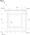
- a light detector 1A illustrated in FIGS. 1 and 2 is a thermal type light detector that detects light (for example, infrared light) by the function as a bolometer and is used for an infrared imager, a thermography, and the like.
- the light detector 1A includes a support substrate 2, a light transmission substrate 3, a pixel portion 4, a first base layer 5, a second base layer 6, a solder layer 7, a reinforcement portion 8, a guide portion 9, and a getter 11.
- the support substrate 2 is, for example, a rectangular plate-shaped Si substrate having an outer shape of about (several mm to dozens of mm) ⁇ (several mm to dozens of mm) and a thickness of about several hundreds of ⁇ m.
- a signal processing circuit unit (not illustrated) is formed within the support substrate 2. The signal processing circuit unit is electrically connected to the pixel portion 4. Furthermore, the signal processing circuit unit may be formed on the support substrate 2.
- the light transmission substrate 3 is disposed on the support substrate 2 so as to overlap the support substrate 2 when viewed from the thickness direction of the support substrate 2 (that is, a direction perpendicular to a first surface 2a of the support substrate 2).
- the light transmission substrate 3 is, for example, a rectangular plate-shaped Si substrate having an outer shape of about (several mm to dozens of mm) ⁇ (several mm to dozens of mm) and a thickness of about several hundreds of ⁇ m.
- the light transmission substrate 3 allows light (for example, infrared light) to be transmitted therethrough.
- the light transmission substrate 3 forms an accommodation space S1 along with the support substrate 2. That is, the light transmission substrate 3 and the support substrate 2 constitute a package having the accommodation space S 1 formed therein.
- a second surface 3a on the side of the support substrate 2 in the light transmission substrate 3 is provided with a concave portion 3b.
- the concave portion 3b is formed in a truncated quadrangular pyramid shape, for example, by dry etching or wet etching.
- the depth of the concave portion 3b is, for example, about a dozen of ⁇ m to several hundreds of ⁇ m.
- the concave portion 3b constitutes a part of the accommodation space S1.
- the pixel portion 4 is provided on the first surface 2a on the side of the light transmission substrate 3 in the support substrate 2 so as to be located in the accommodation space S1.
- the pixel portion 4 is included in the concave portion 3b when viewed from the thickness direction of the support substrate 2.
- the pixel portion 4 has, for example, an outer shape of about (dozens of ⁇ m to dozens of mm) ⁇ (dozens of ⁇ m to dozens of mm).
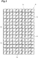
- the pixel portion 4 includes a plurality of light detection elements 10 (see FIG. 3 ) which are arranged in a two-dimensional matrix shape along the first surface 2a.
- Each light detection element 10 includes a bolometer layer whose electrical resistance changes in response to heat generated when light is incident through the light transmission substrate 3.
- the first base layer 5 is provided on the first surface 2a of the support substrate 2 so as to surround the pixel portion 4 when viewed from the thickness direction of the support substrate 2.
- the first base layer 5 is formed in, for example, a rectangular ring shape and includes four first corner portions 5a. An inner edge of the first base layer 5 of each first corner portion 5a becomes a corner when viewed from the thickness direction of the support substrate 2.
- the second base layer 6 is provided on the second surface 3a of the light transmission substrate 3 so as to surround the pixel portion 4 and to overlap the first base layer 5 when viewed from the thickness direction of the support substrate 2.
- the second base layer 6 is formed in, for example, a rectangular ring shape and includes four second corner portions 6a. Four second corner portions 6a respectively overlap four first corner portions 5a when viewed from the thickness direction of the support substrate 2. An inner edge of the second base layer 6 of each second corner portion 6a becomes a corner when viewed from the thickness direction of the support substrate 2.
- each of the first base layer 5 and the second base layer 6 is, for example, about dozens of ⁇ m to several hundreds of ⁇ m.
- the thickness of each of the first base layer 5 and the second base layer 6 is, for example, about dozens of nm to several ⁇ m.
- Each of the first base layer 5 and the second base layer 6 is a lamination film including at least one of, for example, Al, AlCu, AlSi, AlSiCu, AlSiTi, Ti, TiN, Cr, Ni, W, WSi 2 , Pt, Pd, Au and Cu.
- Each of the first base layer 5 and the second base layer 6 may be a single layer film including at least one of, for example, the above-described materials.
- the solder layer 7 is disposed between the first base layer 5 and the second base layer 6.
- the solder layer 7 fixes the support substrate 2 and the light transmission substrate 3 to each other and air-tightly seals the accommodation space S1 by eutectic bonding.
- the solder layer 7 is formed in a rectangular ring shape and includes four corner portions 7a. Four corner portions 7a respectively overlap four first corner portions 5a when viewed from the thickness direction of the support substrate 2.
- the width of the solder layer 7 is, for example, about dozens of ⁇ m to several hundreds of ⁇ m.
- the thickness of the solder layer 7 is, for example, about several ⁇ m.
- the material of the solder layer 7 is, for example, Sn/Pb, Sn/Pb/Ag, Sn/Bi/Pb, Sn/Ag/Cu, Sn/Zn/Bi, Sn/Cu, Sn/Ag/Tn/Bi, Sn/Zn/Al, Ni/Sn, Au/Sn, Ag/Sn, Cu/Sn, Au/In, Cu/In, Ag/In, In, Al/Ge, Al/Zn, Bi/Ag, Sn/Sb, Sn/Ag, Sn/Zn, Sn/Bi, Sn/In, Au/Ga, Au/Si, Au/Ge, Au/Si, Al/Si, or Al/Cu/Ge. Furthermore, when the material of the solder layer 7 is
- the reinforcement portion 8 is disposed on the inside of the first corner portion 5a and the second corner portion 6a which overlap each other when viewed from the thickness direction of the support substrate 2.
- the guide portion 9 is disposed between the pixel portion 4 and the first and second corner portions 5a and 6a overlapping each other when viewed from the thickness direction of the support substrate 2. More specifically, the guide portion 9 is provided on the second surface 3a of the light transmission substrate 3 so as to located between the concave portion 3b and the first and second corner portions 5a and 6a overlapping each other when viewed from the thickness direction of the support substrate 2.
- the detail of the reinforcement portion 8 and the guide portion 9 will be described later.
- the getter 11 is disposed in the accommodation space S1. More specifically, the getter 11 is provided on the bottom surface of the concave portion 3b so as to surround the pixel portion 4 when viewed from the thickness direction of the support substrate 2.
- the getter 11 is formed in, for example, a rectangular ring shape.
- the width of the getter 11 is, for example, about dozens of ⁇ m to several mm.
- the thickness of the getter 11 is, for example, about several ⁇ m.
- the getter 11 maintains the vacuum degree of the accommodation space S1 by absorbing a gas in the accommodation space S1.
- the getter 11 maintains, for example, a state in which the accommodation space S1 is depressurized to about several hundreds of mPa.
- the material of the getter 11 is, for example, an alloy including Zr (zirconium) as a main component.
- the pixel portion 4 includes the plurality of light detection elements 10 which are arranged in a two-dimensional matrix shape.
- each light detection element 10 includes the support substrate 2 (precisely, a part of the support substrate 2), a light reflection layer 12, a pair of electrode plugs 13 and 14, and a film body 20.
- the light reflection layer 12 is formed on the first surface 2a of the support substrate 2.
- the light reflection layer 12 faces a light absorption layer 34 to be described later and constitutes an optical resonant structure along with the light absorption layer 34.
- the thickness of the light reflection layer 12 is, for example, about several hundreds of nm.
- the material of the light reflection layer 12 is, for example, a metal material having a high reflectance to light (for example, infrared light) such as Al.
- the pair of electrode plugs 13 and 14 are formed on the first surface 2a of the support substrate 2.
- Each of the electrode plugs 13 and 14 is formed in, for example, a columnar shape.
- the height of each of the electrode plugs 13 and 14 is, for example, about several ⁇ m.
- the material of each of the electrode plugs 13 and 14 is, for example, a metal material such as Ti.
- the pair of electrode plugs 13 and 14 support the film body 20 on the first surface 2a of the support substrate 2 so that a gap S2 is formed between the first surface 2a of the support substrate 2 and the film body 20.
- the film body 20 is disposed so as to be substantially parallel to the first surface 2a of the support substrate 2.
- the distance between the film body 20 and the first surface 2a of the support substrate 2 is, for example, about several ⁇ m.
- the film body 20 includes a light receiving portion 21, a pair of electrode portions 22 and 23, and a pair of beam portions 24 and 25.
- the light receiving portion 21 spreads so as to avoid each of the electrode plugs 13 and 14 when viewed from the thickness direction of the support substrate 2.
- the electrode portion 22 is disposed on the electrode plug 13.
- the electrode portion 23 is disposed on the electrode plug 14.
- the beam portion 24 is provided on one side of the light receiving portion 21 so as to extend along the outer edge of the light receiving portion 21.
- the beam portion 25 is provided on the other side of the light receiving portion 21 so as to extend along the outer edge of the light receiving portion 21.
- the film body 20 has, for example, a rectangular shape when viewed from the thickness direction of the support substrate 2.
- the pair of electrode portions 22 and 23 are respectively provided at diagonal sides of the film body 20.
- the light receiving portion 21, the pair of electrode portions 22 and 23, and the pair of beam portions 24 and 25 are integrally formed.
- a slit 20a is formed to be a series between the light receiving portion 21 and the electrode portion 22 and between the light receiving portion 21 and the beam portion 24.
- a slit 20b is formed to be a series between the light receiving portion 21 and the electrode portion 23 and between the light receiving portion 21 and the beam portion 25.
- the width of each of the beam portions 24 and 25 is, for example, about several ⁇ m and the length of each of the beam portions 24 and 25 is, for example, about dozens to several hundreds of ⁇ m.
- the width of each of the slits 20a and 20b is, for example, about several ⁇ m.
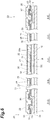
- FIG. 6 is a cross-sectional view of the light detection element 10.
- A-A, B-B, C-C, D-D, and E-E of FIG. 6 are respectively cross-sectional views taken along lines A-A, B-B, C-C, D-D, and E-E of FIG. 5 .
- the film body 20 includes first and second wiring layers 31 and 32, a bolometer layer 33 corresponding to a resistance layer, the light absorption layer 34, and a separation layer 35.
- the first wiring layer 31 and the second wiring layer 32 face each other with a gap G interposed therebetween in the light receiving portion 21 when viewed from the thickness direction of the support substrate 2.
- the gap G extends along a line L.
- the line L extends in a meandering manner so as to connect, for example, the electrode portion 22 and the electrode portion 23 when viewed from the thickness direction of the support substrate 2.
- the line L includes a meandering portion L1.
- the meandering portion L1 includes a plurality of curved portions L2.
- the meandering portion L1 is formed in the light receiving portion 21 by repeating an operation of extending to one side of the light receiving portion 21, turning by, for example, 180° in the curved portion L2, extending to the other side of the light receiving portion 21, turning by, for example, 180° in the curved portion L2, and again extending to one side of the light receiving portion 21.
- one side means one side (for example, a side where the beam portion 24 exists) in a line connecting the electrode portion 22 and the electrode portion 23 when viewed from the thickness direction of the support substrate 2 and the other side means a side (for example, a side where the beam portion 25 exists) opposite to one side in a line connecting the electrode portion 22 and the electrode portion 23 when viewed from the thickness direction of the support substrate 2.
- one side may be one side (for example, a side where the beam portion 24 exists) in a line passing through the center of the film body 20 when viewed from the thickness direction of the support substrate 2 and the other side may be a side (a side where the beam portion 25 exists) opposite to one side in a line passing through the center of the film body 20 when viewed from the thickness direction of the support substrate 2. That is, one side means the side of a first region 34a in the light absorption layer 34 and the other side means the side of a second region 34b in the light absorption layer 34.
- the meandering portion L1 includes a first section L3, a second section L4, a third section L5, and a fourth section L6 when viewed from the thickness direction of the support substrate 2.
- the first section L3 swings to one side by a first swing amount.
- the second section L4 swings to one side by a second swing amount.
- the second section L4 is interposed between two first sections L3 in a direction along a line connecting the electrode portion 22 and the electrode portion 23 when viewed from the thickness direction of the support substrate 2.
- the third section L5 swings to the other side by the first swing amount.
- the fourth section L6 swings to the other side by the second swing amount.
- the fourth section L6 is interposed between two third sections L5 in a direction along a line connecting the electrode portion 22 and the electrode portion 23 when viewed from the thickness direction of the support substrate 2.
- the first swing amount is larger than a predetermined amount.
- the second swing amount is smaller than a predetermined amount.
- the first swing amount is, for example, about a dozen of ⁇ m.
- the second swing amount is, for example, about several ⁇ m.
- the first section L3 extends to one side of the light receiving portion 21 by the first swing amount, turns by, for example, 180° in the curved portion L2, and extends to the other side of the light receiving portion 21 by the first swing amount.
- the fourth section L6 extends to the other side of the light receiving portion 21 by the second swing amount, turns by, for example, 180° in the curved portion L2, and extends to one side of the light receiving portion 21 by the second swing amount.
- the second section L4 extends to one side of the light receiving portion 21 by the second swing amount, turns by, for example, 180° in the curved portion L2, and extends to the other side of the light receiving portion 21 by the second swing amount.
- the third section L5 extends to the other side of the light receiving portion 21 by the first swing amount, turns by, for example, 180° in the curved portion L2, and extends to one side of the light receiving portion 21 by the first swing amount.
- the meandering portion L1 is formed by repeating these operations.
- each of the first section L3, the second section L4, the third section L5, and the fourth section L6 includes the curved portion L2.
- the first wiring layer 31 and the second wiring layer 32 are formed in an elongated shape in a direction along the line L in the light receiving portion 21. That is, the lengths of the first wiring layer 31 and the second wiring layer 32 in a direction along the line L in the light receiving portion 21 are larger than the widths of the first wiring layer 31 and the second wiring layer 32 in a direction perpendicular to the line L when viewed from the thickness direction of the support substrate 2.
- the direction perpendicular to the line L means a direction perpendicular to a tangent line of each position of the line L when viewed from the thickness direction of the support substrate 2.
- the directions perpendicular to the line L at respective positions of the curved portion are different.
- the first wiring layer 31 includes a first edge portion 31a and a third edge portion 31b in the light receiving portion 21.
- Each of the first edge portion 31a and the third edge portion 31b extends along the line L when viewed from the thickness direction of the support substrate 2.
- the first edge portion 31a extends at a position on the side of the line L.
- the third edge portion 31b extends at a position on the side opposite to the line L.
- the second wiring layer 32 includes a second edge portion 32a and a fourth edge portion 32b in the light receiving portion 21.
- Each of the second edge portion 32a and the fourth edge portion 32b extends along the line L when viewed from the thickness direction of the support substrate 2.
- the second edge portion 32a extends at a position on the side of the line L.
- the fourth edge portion 32b extends at a position on the side opposite to the line L.
- the first edge portion 31a and the second edge portion 32a face each other with the line L interposed therebetween when viewed from the thickness direction of the support substrate 2. That is, the gap G is defined by the first edge portion 31a and the second edge portion 32a when viewed from the thickness direction of the support substrate 2.
- the first edge portion 31a on the side of the line L in the first wiring layer 31, the third edge portion 31b on the side opposite to the line L, the second edge portion 32a on the side of the line L in the second wiring layer 32, and the fourth edge portion 32b on the side opposite to the line L respectively continuously extend when viewed from the thickness direction of the support substrate 2.
- a case in which the edge portion continuously extends means that the edge portion is smoothly formed without the corner portion. That is, the continuously extending edge portion does not include a portion with an infinitesimal curvature radius.
- the minimum value of the curvature radius of each of the first edge portion 31a, the second edge portion 32a, the third edge portion 31b, and the fourth edge portion 32b is larger than 0.01 ⁇ m.
- the length of each of the first wiring layer 31 and the second wiring layer 32 in a direction along the line L in the light receiving portion 21 is, for example, about dozens to several hundreds of ⁇ m when viewed from the thickness direction of the support substrate 2.
- the width of each of the first wiring layer 31 and the second wiring layer 32 in a direction perpendicular to the line L is, for example, about several ⁇ m when viewed from the thickness direction of the support substrate 2.
- the width of the gap G in a direction perpendicular to the line L when viewed from the thickness direction of the support substrate 2 is, for example, about several ⁇ m.
- the thickness of each of the first wiring layer 31 and the second wiring layer 32 is, for example, about dozens to several hundreds of nm.
- the first wiring layer 31 extends from the light receiving portion 21 to the electrode portion 22 through the beam portion 24.
- the first wiring layer 31 is formed on the electrode plug 13 in the electrode portion 22.
- the first wiring layer 31 is electrically connected to the electrode plug 13.
- the second wiring layer 32 extends from the light receiving portion 21 to the electrode portion 23 through the beam portion 25.
- the second wiring layer 32 is formed on the electrode plug 14 in the electrode portion 23.
- the second wiring layer 32 is electrically connected to the electrode plug 14.
- the material of each of the first wiring layer 31 and the second wiring layer 32 is, for example, a metal material such as Ti.
- the bolometer layer 33 is formed in the light receiving portion 21 so as to cover the first wiring layer 31 and the second wiring layer 32 from the side opposite to the support substrate 2.
- the bolometer layer 33 is formed in the light receiving portion 21 so as to cover the surfaces opposite to the support substrate 2 in the first wiring layer 31 and the second wiring layer 32 and the side surfaces of the first wiring layer 31 and the second wiring layer 32. That is, the bolometer layer 33 is disposed in the gap G.
- the bolometer layer 33 is formed on the surfaces opposite to the support substrate 2 in the first wiring layer 31 and the second wiring layer 32 in the electrode portions 22 and 23 and the beam portions 24 and 25.
- the bolometer layer 33 is electrically connected to each of the first wiring layer 31 and the second wiring layer 32.
- the thickness of the bolometer layer 33 is, for example, about dozens to several hundreds of nm.
- the bolometer layer 33 has an electrical resistance depending on a temperature.
- the material of the bolometer layer 33 is, for example, a material such as amorphous silicon (a-Si) which has a large change in electrical resistivity due to a change in temperature.
- the light absorption layer 34 faces the first surface 2a of the support substrate 2 in the light receiving portion 21.
- the light absorption layer 34 is disposed on the side opposite to the support substrate 2 with respect to the bolometer layer 33.
- the light absorption layer 34 spreads to the substantially entire region of the light receiving portion 21 when viewed from the thickness direction of the support substrate 2.
- the thickness of the light absorption layer 34 is, for example, about a dozen of nm.
- the material of the light absorption layer 34 is, for example, WSi 2 or Ti.
- the separation layer 35 is disposed between each of the first wiring layer 31 and the light absorption layer 34, and the second wiring layer 32 and the absorption layer 34. Specifically, the separation layer 35 is formed on the surface opposite to the support substrate 2 in the bolometer layer 33 in the light receiving portion 21, the beam portions 24 and 25, and the electrode portions 22 and 23. Then, the light absorption layer 34 is formed on the surface opposite to the support substrate 2 of the separation layer 35 in the light receiving portion 21.
- the thickness of the separation layer 35 is, for example, about several hundreds of nm. The thickness of the separation layer 35 is larger than the thickness of each of the first wiring layer 31, the second wiring layer 32, the bolometer layer 33, and the light absorption layer 34.
- the material of the separation layer 35 is, for example, a silicon nitride film (SiN) or the like.
- the light absorption layer 34 includes the first region 34a and the second region 34b when viewed from the thickness direction of the support substrate 2.
- the first region 34a spreads to the opposite side of the second wiring layer 32 with respect to the first wiring layer 31 when viewed from the thickness direction of the support substrate 2.
- the second region 34b spreads to the opposite side of the first wiring layer 31 with respect to the second wiring layer 32 when viewed from the thickness direction of the support substrate 2.
- the total area of the first wiring layer 31 and the second wiring layer 32 is smaller than the area of each of the first region 34a and the second region 34b when viewed from the thickness direction of the support substrate 2.
- first region 34a and the second region 34b of the light absorption layer 34 are formed on the bolometer layer 33 with the separation layer 35 interposed therebetween. Further, the bolometer layer 33 and the separation layer 35 are continuously formed throughout the first region 34a and the second region 34b.
- the film body 20 is provided with through-holes 20c and 20d.
- the through-holes 20c and 20d are holes through which an etching gas for removing a sacrificial layer (not illustrated) passes.
- the through-holes 20c and 20d are formed on one side of the second section L4 when viewed from the thickness direction of the support substrate 2. Specifically, the through-hole 20c is located between two first sections L3 in the first region 34a.
- the through-hole 20d is located between two third sections L5 in the second region 34b.
- each of the through-holes 20c and 20d has a circular shape and the diameter is, for example, about several ⁇ m.
- the light detector 1A With the above-described configuration, light is detected as below.
- the light receiving portion 21 and the support substrate 2 are thermally separated from each other by the gap S2. Further, the light receiving portion 21 is thermally separated from the electrode portion 22 and the beam portion 24 by the slit 20a. Further, the light receiving portion 21 is thermally separated from the electrode portion 23 and the beam portion 25 by the slit 20b. For this reason, it is possible to prevent heat generated in the light absorption layer 34 from escaping to the support substrate 2 through the beam portions 24 and 25 and the electrode portions 22 and 23.
- Heat generated in the light absorption layer 34 is transmitted to the bolometer layer 33 through the separation layer 35. Then, the bolometer layer 33 increases in temperature and decreases in electrical resistance due to this heat. Such a change in electrical resistance is transmitted as a signal to the signal processing circuit unit through the first and second wiring layers 31 and 32 and the electrode plugs 13 and 14 electrically connected to the bolometer layer 33. Then, in the signal processing circuit unit, a change in electrical resistance of the bolometer layer 33 is converted into a change in voltage or current and light is detected on the basis of a change in voltage or current.
- the optical resonant structure will be described in detail.
- the incident light A (having a wavelength ⁇ ) which is incident to the light absorption layer 34
- a part is reflected as the reflected light B1 by the light absorption layer 34 and the other part is transmitted through the light absorption layer 34.
- the other part of the incident light A transmitted through the light absorption layer 34 is reflected as the reflected light B2 by the light reflection layer 12.
- the reflected light B1 and the reflected light B2 interfere with each other on the reflection surface of the light absorption layer 34 to be canceled.
- the incident light A is absorbed by the reflection surface of the light absorption layer 34. Heat is generated in the light absorption layer 34 by the energy of the absorbed incident light A.
- the absorption rate of the incident light A is determined by the sheet resistance of the light absorption layer 34 and the optical distance t between the light absorption layer 34 and the light reflection layer 12.
- the thickness of the light absorption layer 34 is set to about 16 nm (when the material of the light absorption layer 34 is WSi 2 ) so that the sheet resistance becomes a vacuum impedance (377 ⁇ /sq). Accordingly, the amplitude of the reflected light B1 reflected by the light absorption layer 34 matches the amplitude of the reflected light B2 reflected by the light reflection layer 12. For this reason, the reflected light B1 and the reflected light B2 efficiently interfere with each other to be cancelled in the reflection surface of the light absorption layer 34. Thus, the absorption rate of the incident light A is improved.
- the reinforcement portion 8 is integrally formed with the solder layer 7 by the same material as that of the solder layer 7.
- the wettability of the guide portion 9 with respect to the material forming the reinforcement portion 8 is higher than the wettability of the support substrate 2 and the light transmission substrate 3 with respect to the material forming the reinforcement portion 8.
- the guide portion 9 is, for example, a lamination film including at least one of Al, AlCu, AlSi, AlSiCu, AlSiTi, Ti, TiN, Cr, Ni, W, WSi 2 , Pt, Pd, Au, and Cu.
- the guide portion 9 may be, for example, a single layer film including any one of the above-described materials.
- the thickness of the guide portion 9 is, for example, about dozens of nm to several ⁇ m.
- the guide portion 9 is formed on the second surface 3a of the light transmission substrate 3 so as to fill the inner corner of the second corner portion 6a of the second base layer 6.
- the guide portion 9 moves away from the second base layer 6 in the second surface 3a of the light transmission substrate 3.
- An inner edge 9a of the guide portion 9 is curved (smoothly curved) in a concave shape when viewed from the thickness direction of the support substrate 2.
- the reinforcement portion 8 extends from the corner portion 7a of the solder layer 7 to the guide portion 9 and reaches the guide portion 9. That is, the reinforcement portion 8 reaches the second surface 3a of the light transmission substrate 3 inside the first corner portion 5a and the second corner portion 6a overlapping each other when viewed from the thickness direction of the support substrate 2.
- the reinforcement portion 8 engages with the inside of the second base layer 6.
- An inner edge 8a of the reinforcement portion 8 overlaps the inner edge 9a of the guide portion 9 when viewed from the thickness direction of the support substrate 2 and is curved (smoothly curved) in a concave shape.
- a case in which the reinforcement portion 8 reaches the second surface 3a of the light transmission substrate 3 includes a "case in which the reinforcement portion 8 reaches a film, a layer, or the like (for example, the guide portion 9) formed on the second surface 3a inside the second corner portion 6a of the second base layer 6", a "case in which the reinforcement portion 8 reaches the second surface 3a (contacts the second surface 3a), for example, in a state where the second surface 3 a is not provided with a film, a layer, or the like inside the second corner portion 6a of the second base layer 6", and a "case in which the reinforcement portion 8 extends to the second surface 3a inside the second corner portion 6a of the second base layer 6".
- the reinforcement portion 8 is disposed between the second corner portion 6a and the pixel portion 4 when viewed from the thickness direction of the support substrate 2.
- the reinforcement portion 8 is disposed between the second corner portion 6a and the getter 11 when viewed from the thickness direction of the support substrate 2.
- the reinforcement portion 8 is disposed between the second corner portion 6a and the concave portion 3b when viewed from the thickness direction of the support substrate 2.
- the thickness of the reinforcement portion 8 gradually decreases from the solder layer 7 toward the pixel portion 4.
- the reinforcement portion 8 is disposed at each of a position inside one first corner portion 5a and one second corner portion 6a overlapping each other when viewed from the thickness direction of the support substrate 2 and a position inside the other first corner portion 5a and the other second corner portion 6a overlapping each other when viewed from the thickness direction of the support substrate 2.
- the reinforcement portion 8 is integrally formed with the solder layer 7 and reaches the second surface 3a inside the first corner portion 5a and the second corner portion 6a. Accordingly, the joint portion between the solder layer 7 and the light transmission substrate 3 is reinforced by the reinforcement portion 8. Thus, the joint portion between the solder layer 7 and the light transmission substrate 3 is not easily broken even when the vacuum degree of the accommodation space S1 is increased while thinning the light transmission substrate 3 in order to improve the light detection sensitivity. Thus, according to the light detector 1A, it is possible to improve the light detection sensitivity and to suppress the package breakage.
- the solder layer 7 is, for example, heated and melted so as to fix the support substrate 2 and the light transmission substrate 3 to each other and to air-tightly seal the accommodation space S1.
- each member constituting the light detector 1A expands and contracts and hence stress is generated in each member.
- the solder layer 7 reacts eutectically, the solder layer 7 also expands and contracts and hence stress is generated in the solder layer 7.
- the width of the solder layer 7, the width of the first base layer 5, the width of the second base layer 6, and the like are widened, stress generated during the expansion and contraction thereof increases.
- the solder layer 7 is swollen from the first corner portion 5a and the second corner portion 6a so as to form the reinforcement portion 8, stress generated in the solder layer 7 can be reduced. Furthermore, when stress generated in the solder layer 7 increases, a solder material may be blown into the accommodation space S1 so that the light detection element 10 may be contaminated. In the light detector 1A, such an accident can be also prevented.
- the width of each of the second base layer 6 and the guide portion 9 is narrowed and hence stress generated in each of the second base layer 6 and the guide portion 9 during the expansion and contraction can be reduced. Furthermore, when the guide portion 9 is provided in the first surface 2a, the width of each of the first base layer 5 and the guide portion 9 is narrowed and hence stress generated in each of the first base layer 5 and the guide portion 9 during the expansion and contraction can be reduced.
- the reinforcement portion 8 integrally formed with the solder layer 7 engages with the inside of the second base layer 6, it is possible to increase the package strength by an anchor effect. Furthermore, even when the reinforcement portion 8 integrally formed with the solder layer 7 engages with the inside of the first base layer 5, it is possible to increase the package strength by the anchor effect.
- the light detector 1A since it is possible to increase the package strength while suppressing stress generated in each member when forming the package, it is possible to suppress the package breakage.
- the reinforcement portion 8 integrally formed with the solder layer 7 is disposed inside the first corner portion 5a and the second corner portion 6a. For that reason, as compared with a case in which the reinforcement portion 8 is disposed in a region other than the inside of the first corner portion 5a and the second corner portion 6a in the region along the inner edges of the first base layer 5 and the second base layer 6, it is possible to suppress a decrease in opening ratio of the light transmission substrate 3 due to the reinforcement portion 8 (a ratio occupied by the region through which light is transmitted in the light transmission substrate 3 when viewed from the thickness direction of the support substrate 2) and to secure the arrangement region of the getter 11.
- the plurality of light detection elements 10 are arranged in a two-dimensional matrix shape.
- the support substrate 2 and the light transmission substrate 3 increase in size and the light transmission substrate 3 is easily deformed due to a pressure difference between the inside and the outside of the accommodation space S1.
- the reinforcement portion 8 integrally formed with the solder layer 7 reaches the second surface 3a of the light transmission substrate 3 inside the first corner portion 5a of the first base layer 5 and the second corner portion 6a of the second base layer 6.
- the reinforcement portion 8 reaches the second surface 3a of the light transmission substrate 3. According to this configuration, since the joint portion between the solder layer 7 and the light transmission substrate 3 is reinforced by the reinforcement portion 8, it is possible to more reliably suppress the package breakage. Further, since the reinforcement portion 8 contacts the light detection element 10 provided on the first surface 2a, it is possible to more reliably suppress the contamination or breakage of the light detection element 10.
- the first base layer 5 includes the pair of first corner portions 5a which face each other with the accommodation space S1 interposed therebetween when viewed from the thickness direction of the support substrate 2 and the second base layer 6 includes the pair of second corner portions 6a which respectively overlap the pair of first corner portions 5a when viewed from the thickness direction of the support substrate 2.
- the reinforcement portion 8 is disposed at each of a position inside one first corner portion 5a and one second corner portion 6a overlapping each other when viewed from the thickness direction of the support substrate 2 and a position inside the other first corner portion 5a and the other second corner portion 6a overlapping each other when viewed from the thickness direction of the support substrate 2. According to this configuration, it is possible to reinforce the light transmission substrate 3 with a good balance while suppressing an increase in the number of the reinforcement portions 8.
- the inner edge 8a of the reinforcement portion 8 is curved in a concave shape when viewed from the thickness direction of the support substrate 2. According to this configuration, since a range of forming the reinforcement portion 8 is controlled, it is possible to suppress a decrease in opening ratio of the light transmission substrate 3 and to suppress an individual difference in the vacuum degree of the accommodation space S1 and the reinforcement degree of the light transmission substrate 3.
- the guide portion 9 is provided in the second surface 3a of the light transmission substrate 3 so as to be located between the pixel portion 4 and the first and second corner portions 5a and 6a overlapping each other when viewed from the thickness direction of the support substrate 2. Then, the wettability of the guide portion 9 with respect to the material forming the reinforcement portion 8 is higher than the wettability of the support substrate 2 and the light transmission substrate 3 with respect to the material forming the reinforcement portion 8 and the reinforcement portion 8 reaches the guide portion 9. According to this configuration, since a range of forming the reinforcement portion 8 is controlled, it is possible to suppress a decrease in opening ratio of the light transmission substrate 3 and to suppress an individual difference in the vacuum degree of the accommodation space S1 and the reinforcement degree of the light transmission substrate 3.
- the light transmission substrate 3 is provided with the concave portion 3b forming a part of the accommodation space S1. According to this configuration, it is possible to increase the light transmittance of the light transmission substrate 3 by thinning a region through which light is transmitted in the light transmission substrate 3.
- the first base layer 5, the second base layer 6, and the solder layer 7 overlap one another when viewed from the thickness direction of the support substrate 2. According to this configuration, it is possible to simplify a manufacturing process by patterning the first base layer 5, the second base layer 6, and the solder layer 7 in the same step.
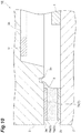
- a light detector 1B is mainly different from the above-described light detector 1A in that the second surface 3a of the light transmission substrate 3 is not provided with the guide portion 9 and the second surface 3a of the light transmission substrate 3 is provided with a groove 3c.
- the second surface 3a of the light transmission substrate 3 is provided with the groove 3c.
- the groove 3c is formed in a rectangular ring shape so as to pass between the pixel portion 4 and the first and second corner portions 5a and 6a overlapping each other when viewed from the thickness direction of the support substrate 2 and to pass between the pixel portion 4 and a group of the first base layer 5, the second base layer 6, and the solder layer 7.
- the groove 3c surrounds the concave portion 3b when viewed from the thickness direction of the support substrate 2.
- the width of the groove 3c is, for example, about several ⁇ m to several hundreds of ⁇ m.
- the depth of the groove 3c is, for example, about dozens of ⁇ m to several hundreds of ⁇ m.
- the reinforcement portion 8 reaches the second surface 3a (contacts the second surface 3a) inside each second corner portion 6a of the second base layer 6 and stays inside the groove 3c.
- the reinforcement portion 8 integrally formed with the solder layer 7 reaches the second surface 3a of the light transmission substrate 3 inside the first corner portion 5a of the first base layer 5 and the second corner portion 6a of the second base layer 6.
- the reinforcement portion 8 reaches the second surface 3a of the light transmission substrate 3 even when the reinforcement portion 8 does not reach the inside of the groove 3c and the second surface 3a of the light transmission substrate 3 is not provided with the groove 3c.
- the groove 3c is formed in the second surface 3a of the light transmission substrate 3 so as to pass between the pixel portion 4 and the first and second corner portions 5a and 6a overlapping each other when viewed from the thickness direction of the support substrate 2. According to this configuration, since a range of forming the reinforcement portion 8 is controlled, it is possible to suppress a decrease in opening ratio of the light transmission substrate 3 and to suppress an individual difference in the vacuum degree of the accommodation space S1 and the reinforcement degree of the light transmission substrate 3.
- a light detector 1C is mainly different from the above-described light detector 1A in that the second surface 3a of the light transmission substrate 3 is not provided with the guide portion 9 and the reinforcement portion 8 reaches the concave portion 3b.
- the reinforcement portion 8 reaches the second surface 3a (contacts the second surface 3a) inside each second corner portion 6a of the second base layer 6 and stays in the corner of the concave portion 3b inside the concave portion 3b.
- the reinforcement portion 8 integrally formed with the solder layer 7 reaches the second surface 3a of the light transmission substrate 3 inside the first corner portion 5a of the first base layer 5 and the second corner portion 6a of the second base layer 6.
- the reinforcement portion 8 reaches the second surface 3a of the light transmission substrate 3 even when the reinforcement portion 8 does not reach the inside of the concave portion 3b and the second surface 3a of the light transmission substrate 3 is not provided with the concave portion 3b.
- the reinforcement portion 8 reaches the inside of the concave portion 3b. According to this configuration, it is possible to increase the light transmittance of the light transmission substrate 3 by thinning a region through which light is transmitted in the light transmission substrate 3. Further, it is possible to reinforce a region through which light is transmitted in the light transmission substrate 3.
- the pixel portion 4 may include one light detection element 10.
- the first base layer 5 may include one or three or more first corner portions 5a.
- the second base layer 6 may include one or three or more second corner portions 6a.
- the reinforcement portion 8 may reach both of the first surface 2a of the support substrate 2 and the second surface 3a of the light transmission substrate 3. According to this configuration, since the joint portion between the solder layer 7 and the light transmission substrate 3 is reinforced by the reinforcement portion 8, the package breakage can be more reliably suppressed. Further, the strength of the package including the support substrate 2 and the light transmission substrate 3 is improved by the anchor effect. For example, when a load is applied to the support substrate 2 and the light transmission substrate 3 in a direction where both substrates are separated from each other in the thickness direction of the support substrate 2, the support substrate 2 and the light transmission substrate 3 are not easily separated from each other by the anchor effect. Further, for example, when a load is applied to the support substrate 2 and the light transmission substrate 3 in a direction along the first surface 2a of the support substrate 2, the positional deviation of the support substrate 2 and the light transmission substrate 3 hardly occurs due to the anchor effect.
- a case in which the reinforcement portion 8 reaches the first surface 2a of the support substrate 2 includes a "case in which the reinforcement portion 8 reaches a film, a layer, or the like (for example, the guide portion 9) formed on the first surface 2a inside the first corner portion 5a of the first base layer 5", a "case in which the reinforcement portion 8 reaches the first surface 2a (contacts the first surface 2a), for example, without forming a film, a layer, or the like on the first surface 2a inside the first corner portion 5a of the first base layer 5", and a "case in which the reinforcement portion 8 extends to the first surface 2a inside the first corner portion 5a of the first base layer 5".
- the reinforcement portion 8 may reach only the first surface 2a of the support substrate 2. According to this configuration, since a force generated when expanding the solder layer 7 is released in the corner portion 7a of the solder layer 7, a load is not easily applied to the light transmission substrate 3 of the corner portion 7a of the solder layer 7.
- the guide portion 9 may be provided on the first surface 2a. Specifically, the guide portion 9 is provided on the surface where at least the reinforcement portion 8 reaches in the first surface 2a and the second surface 3a.
- the guide portion 9 provided in the first surface 2a of the support substrate 2 may be integrally formed with the first base layer 5. At this time, the guide portion 9 may be formed as a part of the first base layer 5. Further, the guide portion 9 provided in the second surface 3a of the light transmission substrate 3 may be integrally formed with the second base layer 6. At this time, the guide portion 9 may be formed as a part of the second base layer 6. Further, the guide portion 9 may be formed so as to surround the light detection element 10 (the pixel portion 4) when viewed from the thickness direction of the support substrate 2.
- the guide portion 9 may be formed in a ring shape so as to pass between the pixel portion 4 and the first and second corner portions 5a and 6a overlapping each other when viewed from the thickness direction of the support substrate 2 and to pass between the pixel portion 4 and a group of the first base layer 5, the second base layer 6, and the solder layer 7.
- the groove 3c may be formed on the first surface 2a. Specifically, the groove 3c is formed on the surface where at least the reinforcement portion 8 reaches in the first surface 2a and the second surface 3a.
- the groove 3c may not surround the pixel portion 4 when viewed from the thickness direction of the support substrate 2 as long as the groove is formed between the pixel portion 4 and the first and second corner portions 5a and 6a overlapping each other when viewed from the thickness direction of the support substrate 2.
- the light detector 1B may not be provided with the groove 3c.
- the reinforcement portion 8 may not reach the inside of the groove 3c.
- first base layer 5 of each first corner portion 5a may be curved (smoothly curved) in a concave shape when viewed from the thickness direction of the support substrate 2.
- first base layer 5 of each first corner portion 5a may be curved (smoothly curved) in a concave shape when viewed from the thickness direction of the support substrate 2.
- second base layer 6 of each second corner portion 6a may be curved (smoothly curved) in a concave shape when viewed from the thickness direction of the support substrate 2.
- 1A, 1B, 1C light detector
- 2 support substrate
- 2a first surface
- 3 light transmission substrate
- 3a second surface
- 3b concave portion
- 3c groove
- 5 first base layer
- 5a first corner portion
- 6 second base layer
- 6a second corner portion
- 7 solder layer
- 8 reinforcement portion
- 8a inner edge
- 9 guide portion
- 10 light detection element
- 33 bolometer layer
- S1 accommodation space.
Landscapes
- Physics & Mathematics (AREA)
- General Physics & Mathematics (AREA)
- Spectroscopy & Molecular Physics (AREA)
- Chemical & Material Sciences (AREA)
- Engineering & Computer Science (AREA)
- Nanotechnology (AREA)
- Photometry And Measurement Of Optical Pulse Characteristics (AREA)
Abstract
A light detector includes: a support substrate; a light transmission substrate which forms an accommodation space along with the support substrate; a light detection element which is located in the accommodation space and includes a bolometer layer; a first base layer which includes a first corner portion; a second base layer which includes a second corner portion; a solder layer which is disposed between the first base layer and the second base layer, fixes the support substrate and the light transmission substrate to each other, and air-tightly seals the accommodation space; and a reinforcement portion which is integrally formed with the solder layer by the same material as that of the solder layer, in which the reinforcement portion reaches at least one of the first surface side and the second surface side inside the first corner portion and the second corner portion.
Description
- An aspect of the invention relates to a light detector which includes a light detection element such as a microbolometer.
- There is known a light detector including a support substrate and a light transmission substrate which form an accommodation space, a light detection element which is a microbolometer or the like provided on the support substrate so as to be located in the accommodation space, and a solder layer which fixes the support substrate and the light transmission substrate to each other and air-tightly seals the accommodation space (for example, see Patent Literature 1).
- Patent Literature 1: Japanese Unexamined Patent Publication No.
2013-543268 - In the above-described light detector, a method of increasing light transmittance by thinning the light transmission substrate or thermally isolating the light detection element from the outside by increasing a vacuum degree of the accommodation space is considered in order to improve light detection sensitivity. However, when the light transmission substrate is thinned, the light transmission substrate is easily deformed. For that reason, since a load is applied to the light transmission substrate or a joint portion between the solder layer and the light transmission substrate to be broken due to external stress or a pressure difference between the inside and the outside of the accommodation space when the vacuum degree of the accommodation space is increased, there is concern that the air-tightness of the accommodation space may be damaged.
- Therefore, an aspect of the invention is to provide a light detector capable of improving light detection sensitivity and suppressing package breakage.
- A light detector according to an aspect of the invention includes: a support substrate; a light transmission substrate which is disposed on the support substrate and forms an accommodation space along with the support substrate; a light detection element which is provided on the support substrate so as to be located in the accommodation space and includes a bolometer layer whose electrical resistance changes in response to heat generated when light is incident through the light transmission substrate; a first base layer which is provided on a first surface on the side of the light transmission substrate in the support substrate so as to surround the light detection element when viewed from a thickness direction of the support substrate; a second base layer which is provided on a second surface on the side of the support substrate in the light transmission substrate so as to surround the light detection element and overlap the first base layer when viewed from the thickness direction of the support substrate; a solder layer which is disposed between the first base layer and the second base layer, fixes the support substrate and the light transmission substrate to each other, and air-tightly seals the accommodation space; and a reinforcement portion which is integrally formed with the solder layer by the same material as that of the solder layer, in which the first base layer includes a first corner portion, in which the second base layer includes a second corner portion which overlaps the first corner portion when viewed from the thickness direction of the support substrate, and in which the reinforcement portion reaches at least one of the first surface side and the second surface side inside the first corner portion and the second corner portion overlapping each other when viewed from the thickness direction of the support substrate.
- In the light detector, the reinforcement portion which is integrally formed with the solder layer reaches at least one of the first surface side of the support substrate and the second surface side of the light transmission substrate inside the first corner portion of the first base layer and the second corner portion of the second base layer. Accordingly, it is possible to suppress the package breakage due to a load applied to the light transmission substrate or the joint portion between the solder layer and the light transmission substrate even when the vacuum degree of the accommodation space is increased while thinning the light transmission substrate in order to improve the light detection sensitivity. Thus, according to the light detector, it is possible to improve the light detection sensitivity and to suppress the package breakage.
- The light detector according to an aspect of the invention may include a plurality of the light detection elements and the plurality of light detection elements may be arranged in a two-dimensional matrix shape. In this configuration, as compared with a case in which one light detection element is provided, the support substrate and the light transmission substrate increase in size and the light transmission substrate is easily deformed due to a pressure difference between the inside and the outside of the accommodation space. For that reason, it is particularly important that the reinforcement portion integrally formed with the solder layer reaches at least one of the first surface side of the support substrate and the second surface side of the light transmission substrate inside the first corner portion of the first base layer and the second corner portion of the second base layer.
- In the light detector according to an aspect of the invention, the reinforcement portion may reach at least the second surface side. According to this configuration, since the joint portion between the solder layer and the light transmission substrate is reinforced by the reinforcement portion, it is possible to more reliably suppress the package breakage.
- In the light detector according to an aspect of the invention, the first base layer may include a pair of the first corner portions which face each other with the accommodation space interposed therebetween when viewed from the thickness direction of the support substrate, the second base layer may include a pair of the second corner portions which respectively overlap the pair of first corner portions when viewed from the thickness direction of the support substrate, and the reinforcement portion may be disposed at each of a position inside one first corner portion and one second corner portion overlapping each other when viewed from the thickness direction of the support substrate and a position inside the other first corner portion and the other second corner portion overlapping each other when viewed from the thickness direction of the support substrate. According to this configuration, it is possible to reinforce the light transmission substrate with a good balance while suppressing an increase in the number of the reinforcement portions.
- In the light detector according to an aspect of the invention, an inner edge of the reinforcement portion may be curved in a concave shape when viewed from the thickness direction of the support substrate. According to this configuration, since a range of forming the reinforcement portion is controlled, it is possible to suppress a decrease in opening ratio (a ratio which is occupied by a light transmission region in the light transmission substrate when viewed from the thickness direction of the support substrate) of the light transmission substrate and to suppress an individual difference in the vacuum degree of the accommodation space and the reinforcement degree of the light transmission substrate.
- The light detector according to an aspect of the invention may further include: a guide portion which is provided in at least one of the first surface and the second surface so as to be located between the light detection element and the first and second corner portions overlapping each other when viewed from the thickness direction of the support substrate, wettability of the guide portion with respect to a material forming the reinforcement portion may be higher than wettability of the support substrate and the light transmission substrate with respect to the material forming the reinforcement portion, and the reinforcement portion may reach the guide portion. According to this configuration, since a range of forming the reinforcement portion is controlled, it is possible to suppress a decrease in opening ratio of the light transmission substrate and to suppress an individual difference in the vacuum degree of the accommodation space and the reinforcement degree of the light transmission substrate.
- In the light detector according to an aspect of the invention, a groove may be formed on at least one of the first surface and the second surface so as to pass between the light detection element and the first and second corner portions overlapping each other when viewed from the thickness direction of the support substrate. According to this configuration, since a range of forming the reinforcement portion is controlled, it is possible to suppress a decrease in opening ratio of the light transmission substrate and to suppress an individual difference in the vacuum degree of the accommodation space and the reinforcement degree of the light transmission substrate.
- In the light detector according to an aspect of the invention, the light transmission substrate may be provided with a concave portion which forms a part of the accommodation space and the reinforcement portion may reach the inside of the concave portion. According to this configuration, it is possible to increase the light transmittance of the light transmission substrate by thinning a region through which light is transmitted in the light transmission substrate. Further, it is possible to reinforce a region through which light is transmitted in the light transmission substrate.
- According to an aspect of the invention, it is possible to provide a light detector capable of improving light detection sensitivity and suppressing package breakage.
-
-
FIG. 1 is a plan view of a light detector of a first embodiment. -
FIG. 2 is a cross-sectional view taken along line II-II illustrated inFIG. 1 . -
FIG. 3 is a plan view of a pixel portion of the light detector illustrated inFIG. 1 . -
FIG. 4 is a perspective view of a light detection element of the pixel portion illustrated inFIG. 3 . -
FIG. 5 is a plan view of the light detection element illustrated inFIG. 4 . -
FIG. 6 is a cross-sectional view of the light detection element illustrated inFIG. 4 . -
FIG. 7 is a view illustrating a principle of an optical resonant structure of the light detection element illustrated inFIG. 4 . -
FIG. 8 is a cross-sectional view taken along line VIII-VIII illustrated inFIG. 1 . -
FIG. 9 is a bottom view of a part of the light detector illustrated inFIG. 1 . -
FIG. 10 is a cross-sectional view of a part of a light detector of a second embodiment. -
FIG. 11 is a bottom view of a part of the light detector illustrated inFIG. 10 . -
FIG. 12 is a bottom view of a part of a light detector of a third embodiment. - Hereinafter, embodiments of the invention will be described in detail with reference to the drawings. Furthermore, in the drawings, the same or equivalent parts will be denoted by the same reference numerals and a redundant description thereof will be omitted.
- A
light detector 1A illustrated inFIGS. 1 and2 is a thermal type light detector that detects light (for example, infrared light) by the function as a bolometer and is used for an infrared imager, a thermography, and the like. As illustrated inFIGS. 1 and2 , thelight detector 1A includes asupport substrate 2, alight transmission substrate 3, apixel portion 4, afirst base layer 5, asecond base layer 6, asolder layer 7, areinforcement portion 8, aguide portion 9, and agetter 11. - The
support substrate 2 is, for example, a rectangular plate-shaped Si substrate having an outer shape of about (several mm to dozens of mm) × (several mm to dozens of mm) and a thickness of about several hundreds of µm. A signal processing circuit unit (not illustrated) is formed within thesupport substrate 2. The signal processing circuit unit is electrically connected to thepixel portion 4. Furthermore, the signal processing circuit unit may be formed on thesupport substrate 2. - The
light transmission substrate 3 is disposed on thesupport substrate 2 so as to overlap thesupport substrate 2 when viewed from the thickness direction of the support substrate 2 (that is, a direction perpendicular to afirst surface 2a of the support substrate 2). Thelight transmission substrate 3 is, for example, a rectangular plate-shaped Si substrate having an outer shape of about (several mm to dozens of mm) × (several mm to dozens of mm) and a thickness of about several hundreds of µm. Thelight transmission substrate 3 allows light (for example, infrared light) to be transmitted therethrough. Thelight transmission substrate 3 forms an accommodation space S1 along with thesupport substrate 2. That is, thelight transmission substrate 3 and thesupport substrate 2 constitute a package having theaccommodation space S 1 formed therein. - A
second surface 3a on the side of thesupport substrate 2 in thelight transmission substrate 3 is provided with aconcave portion 3b. Theconcave portion 3b is formed in a truncated quadrangular pyramid shape, for example, by dry etching or wet etching. The depth of theconcave portion 3b is, for example, about a dozen of µm to several hundreds of µm. Theconcave portion 3b constitutes a part of the accommodation space S1. - The
pixel portion 4 is provided on thefirst surface 2a on the side of thelight transmission substrate 3 in thesupport substrate 2 so as to be located in the accommodation space S1. Thepixel portion 4 is included in theconcave portion 3b when viewed from the thickness direction of thesupport substrate 2. Thepixel portion 4 has, for example, an outer shape of about (dozens of µm to dozens of mm) × (dozens of µm to dozens of mm). Thepixel portion 4 includes a plurality of light detection elements 10 (seeFIG. 3 ) which are arranged in a two-dimensional matrix shape along thefirst surface 2a. Eachlight detection element 10 includes a bolometer layer whose electrical resistance changes in response to heat generated when light is incident through thelight transmission substrate 3. - The
first base layer 5 is provided on thefirst surface 2a of thesupport substrate 2 so as to surround thepixel portion 4 when viewed from the thickness direction of thesupport substrate 2. Thefirst base layer 5 is formed in, for example, a rectangular ring shape and includes fourfirst corner portions 5a. An inner edge of thefirst base layer 5 of eachfirst corner portion 5a becomes a corner when viewed from the thickness direction of thesupport substrate 2. - The
second base layer 6 is provided on thesecond surface 3a of thelight transmission substrate 3 so as to surround thepixel portion 4 and to overlap thefirst base layer 5 when viewed from the thickness direction of thesupport substrate 2. Thesecond base layer 6 is formed in, for example, a rectangular ring shape and includes foursecond corner portions 6a. Foursecond corner portions 6a respectively overlap fourfirst corner portions 5a when viewed from the thickness direction of thesupport substrate 2. An inner edge of thesecond base layer 6 of eachsecond corner portion 6a becomes a corner when viewed from the thickness direction of thesupport substrate 2. - The width of each of the
first base layer 5 and thesecond base layer 6 is, for example, about dozens of µm to several hundreds of µm. The thickness of each of thefirst base layer 5 and thesecond base layer 6 is, for example, about dozens of nm to several µm. Each of thefirst base layer 5 and thesecond base layer 6 is a lamination film including at least one of, for example, Al, AlCu, AlSi, AlSiCu, AlSiTi, Ti, TiN, Cr, Ni, W, WSi2, Pt, Pd, Au and Cu. Each of thefirst base layer 5 and thesecond base layer 6 may be a single layer film including at least one of, for example, the above-described materials. - The
solder layer 7 is disposed between thefirst base layer 5 and thesecond base layer 6. Thesolder layer 7 fixes thesupport substrate 2 and thelight transmission substrate 3 to each other and air-tightly seals the accommodation space S1 by eutectic bonding. Thesolder layer 7 is formed in a rectangular ring shape and includes fourcorner portions 7a. Fourcorner portions 7a respectively overlap fourfirst corner portions 5a when viewed from the thickness direction of thesupport substrate 2. - The width of the
solder layer 7 is, for example, about dozens of µm to several hundreds of µm. The thickness of thesolder layer 7 is, for example, about several µm. The material of thesolder layer 7 is, for example, Sn/Pb, Sn/Pb/Ag, Sn/Bi/Pb, Sn/Ag/Cu, Sn/Zn/Bi, Sn/Cu, Sn/Ag/Tn/Bi, Sn/Zn/Al, Ni/Sn, Au/Sn, Ag/Sn, Cu/Sn, Au/In, Cu/In, Ag/In, In, Al/Ge, Al/Zn, Bi/Ag, Sn/Sb, Sn/Ag, Sn/Zn, Sn/Bi, Sn/In, Au/Ga, Au/Si, Au/Ge, Au/Si, Al/Si, or Al/Cu/Ge. Furthermore, when the material of thesolder layer 7 is Sn/Ag/Cu, Sn/Zn/Bi, or Sn/Cu, for example, Ni, Ge, Co, and Si may be added to the material. - The
reinforcement portion 8 is disposed on the inside of thefirst corner portion 5a and thesecond corner portion 6a which overlap each other when viewed from the thickness direction of thesupport substrate 2. Theguide portion 9 is disposed between thepixel portion 4 and the first andsecond corner portions support substrate 2. More specifically, theguide portion 9 is provided on thesecond surface 3a of thelight transmission substrate 3 so as to located between theconcave portion 3b and the first andsecond corner portions support substrate 2. The detail of thereinforcement portion 8 and theguide portion 9 will be described later. - The
getter 11 is disposed in the accommodation space S1. More specifically, thegetter 11 is provided on the bottom surface of theconcave portion 3b so as to surround thepixel portion 4 when viewed from the thickness direction of thesupport substrate 2. Thegetter 11 is formed in, for example, a rectangular ring shape. The width of thegetter 11 is, for example, about dozens of µm to several mm. The thickness of thegetter 11 is, for example, about several µm. Thegetter 11 maintains the vacuum degree of the accommodation space S1 by absorbing a gas in the accommodation space S1. Thegetter 11 maintains, for example, a state in which the accommodation space S1 is depressurized to about several hundreds of mPa. The material of thegetter 11 is, for example, an alloy including Zr (zirconium) as a main component. - As illustrated in
FIG. 3 , thepixel portion 4 includes the plurality oflight detection elements 10 which are arranged in a two-dimensional matrix shape. As illustrated inFIG. 4 , eachlight detection element 10 includes the support substrate 2 (precisely, a part of the support substrate 2), alight reflection layer 12, a pair of electrode plugs 13 and 14, and afilm body 20. - The
light reflection layer 12 is formed on thefirst surface 2a of thesupport substrate 2. Thelight reflection layer 12 faces alight absorption layer 34 to be described later and constitutes an optical resonant structure along with thelight absorption layer 34. The thickness of thelight reflection layer 12 is, for example, about several hundreds of nm. The material of thelight reflection layer 12 is, for example, a metal material having a high reflectance to light (for example, infrared light) such as Al. - The pair of electrode plugs 13 and 14 are formed on the
first surface 2a of thesupport substrate 2. Each of the electrode plugs 13 and 14 is formed in, for example, a columnar shape. The height of each of the electrode plugs 13 and 14 is, for example, about several µm. The material of each of the electrode plugs 13 and 14 is, for example, a metal material such as Ti. The pair of electrode plugs 13 and 14 support thefilm body 20 on thefirst surface 2a of thesupport substrate 2 so that a gap S2 is formed between thefirst surface 2a of thesupport substrate 2 and thefilm body 20. Thefilm body 20 is disposed so as to be substantially parallel to thefirst surface 2a of thesupport substrate 2. The distance between thefilm body 20 and thefirst surface 2a of thesupport substrate 2 is, for example, about several µm. - As illustrated in
FIGS. 4 and5 , thefilm body 20 includes alight receiving portion 21, a pair ofelectrode portions beam portions light receiving portion 21 spreads so as to avoid each of the electrode plugs 13 and 14 when viewed from the thickness direction of thesupport substrate 2. Theelectrode portion 22 is disposed on theelectrode plug 13. Theelectrode portion 23 is disposed on theelectrode plug 14. Thebeam portion 24 is provided on one side of thelight receiving portion 21 so as to extend along the outer edge of thelight receiving portion 21. Thebeam portion 25 is provided on the other side of thelight receiving portion 21 so as to extend along the outer edge of thelight receiving portion 21. One end of thebeam portion 24 is connected to theelectrode portion 22 and the other end of thebeam portion 24 is connected to thelight receiving portion 21 at a position in the vicinity of theelectrode portion 23. One end of thebeam portion 25 is connected to theelectrode portion 23 and the other end of thebeam portion 25 is connected to thelight receiving portion 21 at a position in the vicinity of theelectrode portion 22. Thefilm body 20 has, for example, a rectangular shape when viewed from the thickness direction of thesupport substrate 2. The pair ofelectrode portions film body 20. - The
light receiving portion 21, the pair ofelectrode portions beam portions slit 20a is formed to be a series between the light receivingportion 21 and theelectrode portion 22 and between the light receivingportion 21 and thebeam portion 24. Aslit 20b is formed to be a series between the light receivingportion 21 and theelectrode portion 23 and between the light receivingportion 21 and thebeam portion 25. The width of each of thebeam portions beam portions slits -
FIG. 6 is a cross-sectional view of thelight detection element 10. A-A, B-B, C-C, D-D, and E-E ofFIG. 6 are respectively cross-sectional views taken along lines A-A, B-B, C-C, D-D, and E-E ofFIG. 5 . As illustrated inFIG. 6 , thefilm body 20 includes first and second wiring layers 31 and 32, abolometer layer 33 corresponding to a resistance layer, thelight absorption layer 34, and aseparation layer 35. - As illustrated in
FIGS. 5 and6 , thefirst wiring layer 31 and thesecond wiring layer 32 face each other with a gap G interposed therebetween in thelight receiving portion 21 when viewed from the thickness direction of thesupport substrate 2. The gap G extends along a line L. The line L extends in a meandering manner so as to connect, for example, theelectrode portion 22 and theelectrode portion 23 when viewed from the thickness direction of thesupport substrate 2. Specifically, the line L includes a meandering portion L1. The meandering portion L1 includes a plurality of curved portions L2. The meandering portion L1 is formed in thelight receiving portion 21 by repeating an operation of extending to one side of thelight receiving portion 21, turning by, for example, 180° in the curved portion L2, extending to the other side of thelight receiving portion 21, turning by, for example, 180° in the curved portion L2, and again extending to one side of thelight receiving portion 21. - In the embodiment, one side means one side (for example, a side where the
beam portion 24 exists) in a line connecting theelectrode portion 22 and theelectrode portion 23 when viewed from the thickness direction of thesupport substrate 2 and the other side means a side (for example, a side where thebeam portion 25 exists) opposite to one side in a line connecting theelectrode portion 22 and theelectrode portion 23 when viewed from the thickness direction of thesupport substrate 2. Further, one side may be one side (for example, a side where thebeam portion 24 exists) in a line passing through the center of thefilm body 20 when viewed from the thickness direction of thesupport substrate 2 and the other side may be a side (a side where thebeam portion 25 exists) opposite to one side in a line passing through the center of thefilm body 20 when viewed from the thickness direction of thesupport substrate 2. That is, one side means the side of afirst region 34a in thelight absorption layer 34 and the other side means the side of asecond region 34b in thelight absorption layer 34. - The meandering portion L1 includes a first section L3, a second section L4, a third section L5, and a fourth section L6 when viewed from the thickness direction of the
support substrate 2. The first section L3 swings to one side by a first swing amount. The second section L4 swings to one side by a second swing amount. The second section L4 is interposed between two first sections L3 in a direction along a line connecting theelectrode portion 22 and theelectrode portion 23 when viewed from the thickness direction of thesupport substrate 2. The third section L5 swings to the other side by the first swing amount. The fourth section L6 swings to the other side by the second swing amount. The fourth section L6 is interposed between two third sections L5 in a direction along a line connecting theelectrode portion 22 and theelectrode portion 23 when viewed from the thickness direction of thesupport substrate 2. The first swing amount is larger than a predetermined amount. The second swing amount is smaller than a predetermined amount. The first swing amount is, for example, about a dozen of µm. The second swing amount is, for example, about several µm. - Specifically, in the
light receiving portion 21, the first section L3 extends to one side of thelight receiving portion 21 by the first swing amount, turns by, for example, 180° in the curved portion L2, and extends to the other side of thelight receiving portion 21 by the first swing amount. Subsequently, the fourth section L6 extends to the other side of thelight receiving portion 21 by the second swing amount, turns by, for example, 180° in the curved portion L2, and extends to one side of thelight receiving portion 21 by the second swing amount. Subsequently, the second section L4 extends to one side of thelight receiving portion 21 by the second swing amount, turns by, for example, 180° in the curved portion L2, and extends to the other side of thelight receiving portion 21 by the second swing amount. Subsequently, the third section L5 extends to the other side of thelight receiving portion 21 by the first swing amount, turns by, for example, 180° in the curved portion L2, and extends to one side of thelight receiving portion 21 by the first swing amount. The meandering portion L1 is formed by repeating these operations. Furthermore, each of the first section L3, the second section L4, the third section L5, and the fourth section L6 includes the curved portion L2. - The
first wiring layer 31 and thesecond wiring layer 32 are formed in an elongated shape in a direction along the line L in thelight receiving portion 21. That is, the lengths of thefirst wiring layer 31 and thesecond wiring layer 32 in a direction along the line L in thelight receiving portion 21 are larger than the widths of thefirst wiring layer 31 and thesecond wiring layer 32 in a direction perpendicular to the line L when viewed from the thickness direction of thesupport substrate 2. The direction perpendicular to the line L means a direction perpendicular to a tangent line of each position of the line L when viewed from the thickness direction of thesupport substrate 2. The directions perpendicular to the line L at respective positions of the curved portion are different. - Specifically, the
first wiring layer 31 includes afirst edge portion 31a and athird edge portion 31b in thelight receiving portion 21. Each of thefirst edge portion 31a and thethird edge portion 31b extends along the line L when viewed from the thickness direction of thesupport substrate 2. Thefirst edge portion 31a extends at a position on the side of the line L. Thethird edge portion 31b extends at a position on the side opposite to the line L. Thesecond wiring layer 32 includes asecond edge portion 32a and afourth edge portion 32b in thelight receiving portion 21. Each of thesecond edge portion 32a and thefourth edge portion 32b extends along the line L when viewed from the thickness direction of thesupport substrate 2. Thesecond edge portion 32a extends at a position on the side of the line L. Thefourth edge portion 32b extends at a position on the side opposite to the line L. - The
first edge portion 31a and thesecond edge portion 32a face each other with the line L interposed therebetween when viewed from the thickness direction of thesupport substrate 2. That is, the gap G is defined by thefirst edge portion 31a and thesecond edge portion 32a when viewed from the thickness direction of thesupport substrate 2. - The
first edge portion 31a on the side of the line L in thefirst wiring layer 31, thethird edge portion 31b on the side opposite to the line L, thesecond edge portion 32a on the side of the line L in thesecond wiring layer 32, and thefourth edge portion 32b on the side opposite to the line L respectively continuously extend when viewed from the thickness direction of thesupport substrate 2. A case in which the edge portion continuously extends means that the edge portion is smoothly formed without the corner portion. That is, the continuously extending edge portion does not include a portion with an infinitesimal curvature radius. For example, the minimum value of the curvature radius of each of thefirst edge portion 31a, thesecond edge portion 32a, thethird edge portion 31b, and thefourth edge portion 32b is larger than 0.01 µm. - The length of each of the
first wiring layer 31 and thesecond wiring layer 32 in a direction along the line L in thelight receiving portion 21 is, for example, about dozens to several hundreds of µm when viewed from the thickness direction of thesupport substrate 2. The width of each of thefirst wiring layer 31 and thesecond wiring layer 32 in a direction perpendicular to the line L is, for example, about several µm when viewed from the thickness direction of thesupport substrate 2. The width of the gap G in a direction perpendicular to the line L when viewed from the thickness direction of thesupport substrate 2 is, for example, about several µm. The thickness of each of thefirst wiring layer 31 and thesecond wiring layer 32 is, for example, about dozens to several hundreds of nm. - The
first wiring layer 31 extends from thelight receiving portion 21 to theelectrode portion 22 through thebeam portion 24. Thefirst wiring layer 31 is formed on theelectrode plug 13 in theelectrode portion 22. Thefirst wiring layer 31 is electrically connected to theelectrode plug 13. Thesecond wiring layer 32 extends from thelight receiving portion 21 to theelectrode portion 23 through thebeam portion 25. Thesecond wiring layer 32 is formed on theelectrode plug 14 in theelectrode portion 23. Thesecond wiring layer 32 is electrically connected to theelectrode plug 14. The material of each of thefirst wiring layer 31 and thesecond wiring layer 32 is, for example, a metal material such as Ti. - The
bolometer layer 33 is formed in thelight receiving portion 21 so as to cover thefirst wiring layer 31 and thesecond wiring layer 32 from the side opposite to thesupport substrate 2. Thebolometer layer 33 is formed in thelight receiving portion 21 so as to cover the surfaces opposite to thesupport substrate 2 in thefirst wiring layer 31 and thesecond wiring layer 32 and the side surfaces of thefirst wiring layer 31 and thesecond wiring layer 32. That is, thebolometer layer 33 is disposed in the gap G. Thebolometer layer 33 is formed on the surfaces opposite to thesupport substrate 2 in thefirst wiring layer 31 and thesecond wiring layer 32 in theelectrode portions beam portions bolometer layer 33 is electrically connected to each of thefirst wiring layer 31 and thesecond wiring layer 32. The thickness of thebolometer layer 33 is, for example, about dozens to several hundreds of nm. Thebolometer layer 33 has an electrical resistance depending on a temperature. The material of thebolometer layer 33 is, for example, a material such as amorphous silicon (a-Si) which has a large change in electrical resistivity due to a change in temperature. - The
light absorption layer 34 faces thefirst surface 2a of thesupport substrate 2 in thelight receiving portion 21. Thelight absorption layer 34 is disposed on the side opposite to thesupport substrate 2 with respect to thebolometer layer 33. Thelight absorption layer 34 spreads to the substantially entire region of thelight receiving portion 21 when viewed from the thickness direction of thesupport substrate 2. The thickness of thelight absorption layer 34 is, for example, about a dozen of nm. The material of thelight absorption layer 34 is, for example, WSi2 or Ti. - The
separation layer 35 is disposed between each of thefirst wiring layer 31 and thelight absorption layer 34, and thesecond wiring layer 32 and theabsorption layer 34. Specifically, theseparation layer 35 is formed on the surface opposite to thesupport substrate 2 in thebolometer layer 33 in thelight receiving portion 21, thebeam portions electrode portions light absorption layer 34 is formed on the surface opposite to thesupport substrate 2 of theseparation layer 35 in thelight receiving portion 21. The thickness of theseparation layer 35 is, for example, about several hundreds of nm. The thickness of theseparation layer 35 is larger than the thickness of each of thefirst wiring layer 31, thesecond wiring layer 32, thebolometer layer 33, and thelight absorption layer 34. The material of theseparation layer 35 is, for example, a silicon nitride film (SiN) or the like. - The
light absorption layer 34 includes thefirst region 34a and thesecond region 34b when viewed from the thickness direction of thesupport substrate 2. Thefirst region 34a spreads to the opposite side of thesecond wiring layer 32 with respect to thefirst wiring layer 31 when viewed from the thickness direction of thesupport substrate 2. Thesecond region 34b spreads to the opposite side of thefirst wiring layer 31 with respect to thesecond wiring layer 32 when viewed from the thickness direction of thesupport substrate 2. The total area of thefirst wiring layer 31 and thesecond wiring layer 32 is smaller than the area of each of thefirst region 34a and thesecond region 34b when viewed from the thickness direction of thesupport substrate 2. - Furthermore, the
first region 34a and thesecond region 34b of thelight absorption layer 34 are formed on thebolometer layer 33 with theseparation layer 35 interposed therebetween. Further, thebolometer layer 33 and theseparation layer 35 are continuously formed throughout thefirst region 34a and thesecond region 34b. - The
film body 20 is provided with through-holes holes holes support substrate 2. Specifically, the through-hole 20c is located between two first sections L3 in thefirst region 34a. The through-hole 20d is located between two third sections L5 in thesecond region 34b. When viewed from the thickness direction of thesupport substrate 2, each of the through-holes - In the
light detector 1A with the above-described configuration, light is detected as below. First, when light is transmitted through thelight transmission substrate 3 and is incident to thelight receiving portion 21, heat is generated in thelight absorption layer 34 constituting the optical resonant structure to be described later. At this time, thelight receiving portion 21 and thesupport substrate 2 are thermally separated from each other by the gap S2. Further, thelight receiving portion 21 is thermally separated from theelectrode portion 22 and thebeam portion 24 by theslit 20a. Further, thelight receiving portion 21 is thermally separated from theelectrode portion 23 and thebeam portion 25 by theslit 20b. For this reason, it is possible to prevent heat generated in thelight absorption layer 34 from escaping to thesupport substrate 2 through thebeam portions electrode portions - Heat generated in the
light absorption layer 34 is transmitted to thebolometer layer 33 through theseparation layer 35. Then, thebolometer layer 33 increases in temperature and decreases in electrical resistance due to this heat. Such a change in electrical resistance is transmitted as a signal to the signal processing circuit unit through the first and second wiring layers 31 and 32 and the electrode plugs 13 and 14 electrically connected to thebolometer layer 33. Then, in the signal processing circuit unit, a change in electrical resistance of thebolometer layer 33 is converted into a change in voltage or current and light is detected on the basis of a change in voltage or current. - Next, the optical resonant structure will be described in detail. As illustrated in
FIG. 7 , in the incident light A (having a wavelength λ) which is incident to thelight absorption layer 34, a part is reflected as the reflected light B1 by thelight absorption layer 34 and the other part is transmitted through thelight absorption layer 34. The other part of the incident light A transmitted through thelight absorption layer 34 is reflected as the reflected light B2 by thelight reflection layer 12. Then, the reflected light B1 and the reflected light B2 interfere with each other on the reflection surface of thelight absorption layer 34 to be canceled. Accordingly, the incident light A is absorbed by the reflection surface of thelight absorption layer 34. Heat is generated in thelight absorption layer 34 by the energy of the absorbed incident light A. - The absorption rate of the incident light A is determined by the sheet resistance of the
light absorption layer 34 and the optical distance t between thelight absorption layer 34 and thelight reflection layer 12. The thickness of thelight absorption layer 34 is set to about 16 nm (when the material of thelight absorption layer 34 is WSi2) so that the sheet resistance becomes a vacuum impedance (377 Ω/sq). Accordingly, the amplitude of the reflected light B1 reflected by thelight absorption layer 34 matches the amplitude of the reflected light B2 reflected by thelight reflection layer 12. For this reason, the reflected light B1 and the reflected light B2 efficiently interfere with each other to be cancelled in the reflection surface of thelight absorption layer 34. Thus, the absorption rate of the incident light A is improved. - Further, the optical distance t is set to be t = (2m - 1)λ/4 (m = 1, 2, 3, ...). Accordingly, the phases of the reflected light B1 and the reflected light B2 deviate from each other by 180°. For this reason, the reflected light B1 and the reflected light B2 efficiently interfere with each other to be cancelled in the reflection surface of the
light absorption layer 34. Thus, the absorption rate of the incident light A is improved. In this way, thelight reflection layer 12 constitutes the optical resonant structure with thelight absorption layer 34. The incident light A is efficiently absorbed as an area of an overlapping portion between thelight reflection layer 12 and thelight absorption layer 34 when viewed from the thickness direction of thesupport substrate 2 becomes wider. - As illustrated in
FIGS. 8 and9 , thereinforcement portion 8 is integrally formed with thesolder layer 7 by the same material as that of thesolder layer 7. The wettability of theguide portion 9 with respect to the material forming thereinforcement portion 8 is higher than the wettability of thesupport substrate 2 and thelight transmission substrate 3 with respect to the material forming thereinforcement portion 8. Theguide portion 9 is, for example, a lamination film including at least one of Al, AlCu, AlSi, AlSiCu, AlSiTi, Ti, TiN, Cr, Ni, W, WSi2, Pt, Pd, Au, and Cu. Theguide portion 9 may be, for example, a single layer film including any one of the above-described materials. The thickness of theguide portion 9 is, for example, about dozens of nm to several µm. - The
guide portion 9 is formed on thesecond surface 3a of thelight transmission substrate 3 so as to fill the inner corner of thesecond corner portion 6a of thesecond base layer 6. Theguide portion 9 moves away from thesecond base layer 6 in thesecond surface 3a of thelight transmission substrate 3. Aninner edge 9a of theguide portion 9 is curved (smoothly curved) in a concave shape when viewed from the thickness direction of thesupport substrate 2. - The
reinforcement portion 8 extends from thecorner portion 7a of thesolder layer 7 to theguide portion 9 and reaches theguide portion 9. That is, thereinforcement portion 8 reaches thesecond surface 3a of thelight transmission substrate 3 inside thefirst corner portion 5a and thesecond corner portion 6a overlapping each other when viewed from the thickness direction of thesupport substrate 2. Thereinforcement portion 8 engages with the inside of thesecond base layer 6. Aninner edge 8a of thereinforcement portion 8 overlaps theinner edge 9a of theguide portion 9 when viewed from the thickness direction of thesupport substrate 2 and is curved (smoothly curved) in a concave shape. - Furthermore, a case in which the
reinforcement portion 8 reaches thesecond surface 3a of thelight transmission substrate 3 includes a "case in which thereinforcement portion 8 reaches a film, a layer, or the like (for example, the guide portion 9) formed on thesecond surface 3a inside thesecond corner portion 6a of thesecond base layer 6", a "case in which thereinforcement portion 8 reaches thesecond surface 3a (contacts thesecond surface 3a), for example, in a state where thesecond surface 3 a is not provided with a film, a layer, or the like inside thesecond corner portion 6a of thesecond base layer 6", and a "case in which thereinforcement portion 8 extends to thesecond surface 3a inside thesecond corner portion 6a of thesecond base layer 6". - The
reinforcement portion 8 is disposed between thesecond corner portion 6a and thepixel portion 4 when viewed from the thickness direction of thesupport substrate 2. Thereinforcement portion 8 is disposed between thesecond corner portion 6a and thegetter 11 when viewed from the thickness direction of thesupport substrate 2. Thereinforcement portion 8 is disposed between thesecond corner portion 6a and theconcave portion 3b when viewed from the thickness direction of thesupport substrate 2. The thickness of thereinforcement portion 8 gradually decreases from thesolder layer 7 toward thepixel portion 4. - When focusing on a pair of
first corner portions 5a facing each other with the accommodation space S1 interposed therebetween when viewed from the thickness direction of thesupport substrate 2 and a pair ofsecond corner portions 6a respectively overlapping the pair offirst corner portions 5a when viewed from the thickness direction of thesupport substrate 2, thereinforcement portion 8 is disposed at each of a position inside onefirst corner portion 5a and onesecond corner portion 6a overlapping each other when viewed from the thickness direction of thesupport substrate 2 and a position inside the otherfirst corner portion 5a and the othersecond corner portion 6a overlapping each other when viewed from the thickness direction of thesupport substrate 2. - As described above, in the
light detector 1A, thereinforcement portion 8 is integrally formed with thesolder layer 7 and reaches thesecond surface 3a inside thefirst corner portion 5a and thesecond corner portion 6a. Accordingly, the joint portion between thesolder layer 7 and thelight transmission substrate 3 is reinforced by thereinforcement portion 8. Thus, the joint portion between thesolder layer 7 and thelight transmission substrate 3 is not easily broken even when the vacuum degree of the accommodation space S1 is increased while thinning thelight transmission substrate 3 in order to improve the light detection sensitivity. Thus, according to thelight detector 1A, it is possible to improve the light detection sensitivity and to suppress the package breakage. - Hereinafter, the suppression of the package breakage will be described in more detail. The
solder layer 7 is, for example, heated and melted so as to fix thesupport substrate 2 and thelight transmission substrate 3 to each other and to air-tightly seal the accommodation space S1. When heating thesolder layer 7, each member constituting thelight detector 1A expands and contracts and hence stress is generated in each member. Further, when thesolder layer 7 reacts eutectically, thesolder layer 7 also expands and contracts and hence stress is generated in thesolder layer 7. When the width of thesolder layer 7, the width of thefirst base layer 5, the width of thesecond base layer 6, and the like are widened, stress generated during the expansion and contraction thereof increases. - In the
light detector 1A, since thesolder layer 7 is swollen from thefirst corner portion 5a and thesecond corner portion 6a so as to form thereinforcement portion 8, stress generated in thesolder layer 7 can be reduced. Furthermore, when stress generated in thesolder layer 7 increases, a solder material may be blown into the accommodation space S1 so that thelight detection element 10 may be contaminated. In thelight detector 1A, such an accident can be also prevented. - Similarly, since the
guide portion 9 is separated from thesecond base layer 6, the width of each of thesecond base layer 6 and theguide portion 9 is narrowed and hence stress generated in each of thesecond base layer 6 and theguide portion 9 during the expansion and contraction can be reduced. Furthermore, when theguide portion 9 is provided in thefirst surface 2a, the width of each of thefirst base layer 5 and theguide portion 9 is narrowed and hence stress generated in each of thefirst base layer 5 and theguide portion 9 during the expansion and contraction can be reduced. - Further, since the
reinforcement portion 8 integrally formed with thesolder layer 7 engages with the inside of thesecond base layer 6, it is possible to increase the package strength by an anchor effect. Furthermore, even when thereinforcement portion 8 integrally formed with thesolder layer 7 engages with the inside of thefirst base layer 5, it is possible to increase the package strength by the anchor effect. - As described above, according to the
light detector 1A, since it is possible to increase the package strength while suppressing stress generated in each member when forming the package, it is possible to suppress the package breakage. - Further, the
reinforcement portion 8 integrally formed with thesolder layer 7 is disposed inside thefirst corner portion 5a and thesecond corner portion 6a. For that reason, as compared with a case in which thereinforcement portion 8 is disposed in a region other than the inside of thefirst corner portion 5a and thesecond corner portion 6a in the region along the inner edges of thefirst base layer 5 and thesecond base layer 6, it is possible to suppress a decrease in opening ratio of thelight transmission substrate 3 due to the reinforcement portion 8 (a ratio occupied by the region through which light is transmitted in thelight transmission substrate 3 when viewed from the thickness direction of the support substrate 2) and to secure the arrangement region of thegetter 11. - Further, in the
light detector 1A, the plurality oflight detection elements 10 are arranged in a two-dimensional matrix shape. In this configuration, as compared with a case in which onelight detection element 10 is provided, thesupport substrate 2 and thelight transmission substrate 3 increase in size and thelight transmission substrate 3 is easily deformed due to a pressure difference between the inside and the outside of the accommodation space S1. For that reason, it is particularly important that thereinforcement portion 8 integrally formed with thesolder layer 7 reaches thesecond surface 3a of thelight transmission substrate 3 inside thefirst corner portion 5a of thefirst base layer 5 and thesecond corner portion 6a of thesecond base layer 6. - Further, in the
light detector 1, thereinforcement portion 8 reaches thesecond surface 3a of thelight transmission substrate 3. According to this configuration, since the joint portion between thesolder layer 7 and thelight transmission substrate 3 is reinforced by thereinforcement portion 8, it is possible to more reliably suppress the package breakage. Further, since thereinforcement portion 8 contacts thelight detection element 10 provided on thefirst surface 2a, it is possible to more reliably suppress the contamination or breakage of thelight detection element 10. - Further, in the
light detector 1A, thefirst base layer 5 includes the pair offirst corner portions 5a which face each other with the accommodation space S1 interposed therebetween when viewed from the thickness direction of thesupport substrate 2 and thesecond base layer 6 includes the pair ofsecond corner portions 6a which respectively overlap the pair offirst corner portions 5a when viewed from the thickness direction of thesupport substrate 2. Then, thereinforcement portion 8 is disposed at each of a position inside onefirst corner portion 5a and onesecond corner portion 6a overlapping each other when viewed from the thickness direction of thesupport substrate 2 and a position inside the otherfirst corner portion 5a and the othersecond corner portion 6a overlapping each other when viewed from the thickness direction of thesupport substrate 2. According to this configuration, it is possible to reinforce thelight transmission substrate 3 with a good balance while suppressing an increase in the number of thereinforcement portions 8. - Further, in the
light detector 1A, theinner edge 8a of thereinforcement portion 8 is curved in a concave shape when viewed from the thickness direction of thesupport substrate 2. According to this configuration, since a range of forming thereinforcement portion 8 is controlled, it is possible to suppress a decrease in opening ratio of thelight transmission substrate 3 and to suppress an individual difference in the vacuum degree of the accommodation space S1 and the reinforcement degree of thelight transmission substrate 3. - Further, in the
light detector 1A, theguide portion 9 is provided in thesecond surface 3a of thelight transmission substrate 3 so as to be located between thepixel portion 4 and the first andsecond corner portions support substrate 2. Then, the wettability of theguide portion 9 with respect to the material forming thereinforcement portion 8 is higher than the wettability of thesupport substrate 2 and thelight transmission substrate 3 with respect to the material forming thereinforcement portion 8 and thereinforcement portion 8 reaches theguide portion 9. According to this configuration, since a range of forming thereinforcement portion 8 is controlled, it is possible to suppress a decrease in opening ratio of thelight transmission substrate 3 and to suppress an individual difference in the vacuum degree of the accommodation space S1 and the reinforcement degree of thelight transmission substrate 3. - Further, in the
light detector 1A, thelight transmission substrate 3 is provided with theconcave portion 3b forming a part of the accommodation space S1. According to this configuration, it is possible to increase the light transmittance of thelight transmission substrate 3 by thinning a region through which light is transmitted in thelight transmission substrate 3. - Further, in the
light detector 1A, thefirst base layer 5, thesecond base layer 6, and thesolder layer 7 overlap one another when viewed from the thickness direction of thesupport substrate 2. According to this configuration, it is possible to simplify a manufacturing process by patterning thefirst base layer 5, thesecond base layer 6, and thesolder layer 7 in the same step. - As illustrated in
FIGS. 10 and11 , alight detector 1B is mainly different from the above-describedlight detector 1A in that thesecond surface 3a of thelight transmission substrate 3 is not provided with theguide portion 9 and thesecond surface 3a of thelight transmission substrate 3 is provided with agroove 3c. In thelight detector 1B, thesecond surface 3a of thelight transmission substrate 3 is provided with thegroove 3c. Thegroove 3c is formed in a rectangular ring shape so as to pass between thepixel portion 4 and the first andsecond corner portions support substrate 2 and to pass between thepixel portion 4 and a group of thefirst base layer 5, thesecond base layer 6, and thesolder layer 7. Thegroove 3c surrounds theconcave portion 3b when viewed from the thickness direction of thesupport substrate 2. The width of thegroove 3c is, for example, about several µm to several hundreds of µm. The depth of thegroove 3c is, for example, about dozens of µm to several hundreds of µm. Further, thereinforcement portion 8 reaches thesecond surface 3a (contacts thesecond surface 3a) inside eachsecond corner portion 6a of thesecond base layer 6 and stays inside thegroove 3c. - In the
light detector 1B with the above-described configuration, similarly to the above-describedlight detector 1A, thereinforcement portion 8 integrally formed with thesolder layer 7 reaches thesecond surface 3a of thelight transmission substrate 3 inside thefirst corner portion 5a of thefirst base layer 5 and thesecond corner portion 6a of thesecond base layer 6. Thus, according to thelight detector 1B, it is possible to improve the light detection sensitivity and to suppress the package breakage. Furthermore, this effect is obtained when thereinforcement portion 8 reaches thesecond surface 3a of thelight transmission substrate 3 even when thereinforcement portion 8 does not reach the inside of thegroove 3c and thesecond surface 3a of thelight transmission substrate 3 is not provided with thegroove 3c. - Further, in the
light detector 1B, thegroove 3c is formed in thesecond surface 3a of thelight transmission substrate 3 so as to pass between thepixel portion 4 and the first andsecond corner portions support substrate 2. According to this configuration, since a range of forming thereinforcement portion 8 is controlled, it is possible to suppress a decrease in opening ratio of thelight transmission substrate 3 and to suppress an individual difference in the vacuum degree of the accommodation space S1 and the reinforcement degree of thelight transmission substrate 3. - As illustrated in
FIG. 12 , alight detector 1C is mainly different from the above-describedlight detector 1A in that thesecond surface 3a of thelight transmission substrate 3 is not provided with theguide portion 9 and thereinforcement portion 8 reaches theconcave portion 3b. In thelight detector 1C, thereinforcement portion 8 reaches thesecond surface 3a (contacts thesecond surface 3a) inside eachsecond corner portion 6a of thesecond base layer 6 and stays in the corner of theconcave portion 3b inside theconcave portion 3b. - In the
light detector 1C with the above-described configuration, similarly to the above-describedlight detector 1A, thereinforcement portion 8 integrally formed with thesolder layer 7 reaches thesecond surface 3a of thelight transmission substrate 3 inside thefirst corner portion 5a of thefirst base layer 5 and thesecond corner portion 6a of thesecond base layer 6. Thus, according to thelight detector 1C, it is possible to improve the light detection sensitivity and to suppress the package breakage. Furthermore, this effect is obtained when thereinforcement portion 8 reaches thesecond surface 3a of thelight transmission substrate 3 even when thereinforcement portion 8 does not reach the inside of theconcave portion 3b and thesecond surface 3a of thelight transmission substrate 3 is not provided with theconcave portion 3b. - Further, in the
light detector 1B, thereinforcement portion 8 reaches the inside of theconcave portion 3b. According to this configuration, it is possible to increase the light transmittance of thelight transmission substrate 3 by thinning a region through which light is transmitted in thelight transmission substrate 3. Further, it is possible to reinforce a region through which light is transmitted in thelight transmission substrate 3. - Although the first, second, and third embodiments of the invention have been described above, an aspect of the invention is not limited to the above-described first, second, and third embodiments. For example, the
pixel portion 4 may include onelight detection element 10. Further, thefirst base layer 5 may include one or three or morefirst corner portions 5a. Similarly, thesecond base layer 6 may include one or three or moresecond corner portions 6a. - Further, the
reinforcement portion 8 may reach both of thefirst surface 2a of thesupport substrate 2 and thesecond surface 3a of thelight transmission substrate 3. According to this configuration, since the joint portion between thesolder layer 7 and thelight transmission substrate 3 is reinforced by thereinforcement portion 8, the package breakage can be more reliably suppressed. Further, the strength of the package including thesupport substrate 2 and thelight transmission substrate 3 is improved by the anchor effect. For example, when a load is applied to thesupport substrate 2 and thelight transmission substrate 3 in a direction where both substrates are separated from each other in the thickness direction of thesupport substrate 2, thesupport substrate 2 and thelight transmission substrate 3 are not easily separated from each other by the anchor effect. Further, for example, when a load is applied to thesupport substrate 2 and thelight transmission substrate 3 in a direction along thefirst surface 2a of thesupport substrate 2, the positional deviation of thesupport substrate 2 and thelight transmission substrate 3 hardly occurs due to the anchor effect. - Furthermore, a case in which the
reinforcement portion 8 reaches thefirst surface 2a of thesupport substrate 2 includes a "case in which thereinforcement portion 8 reaches a film, a layer, or the like (for example, the guide portion 9) formed on thefirst surface 2a inside thefirst corner portion 5a of thefirst base layer 5", a "case in which thereinforcement portion 8 reaches thefirst surface 2a (contacts thefirst surface 2a), for example, without forming a film, a layer, or the like on thefirst surface 2a inside thefirst corner portion 5a of thefirst base layer 5", and a "case in which thereinforcement portion 8 extends to thefirst surface 2a inside thefirst corner portion 5a of thefirst base layer 5". - Further, the
reinforcement portion 8 may reach only thefirst surface 2a of thesupport substrate 2. According to this configuration, since a force generated when expanding thesolder layer 7 is released in thecorner portion 7a of thesolder layer 7, a load is not easily applied to thelight transmission substrate 3 of thecorner portion 7a of thesolder layer 7. - Further, the
guide portion 9 may be provided on thefirst surface 2a. Specifically, theguide portion 9 is provided on the surface where at least thereinforcement portion 8 reaches in thefirst surface 2a and thesecond surface 3a. - Further, the
guide portion 9 provided in thefirst surface 2a of thesupport substrate 2 may be integrally formed with thefirst base layer 5. At this time, theguide portion 9 may be formed as a part of thefirst base layer 5. Further, theguide portion 9 provided in thesecond surface 3a of thelight transmission substrate 3 may be integrally formed with thesecond base layer 6. At this time, theguide portion 9 may be formed as a part of thesecond base layer 6. Further, theguide portion 9 may be formed so as to surround the light detection element 10 (the pixel portion 4) when viewed from the thickness direction of thesupport substrate 2. For example, theguide portion 9 may be formed in a ring shape so as to pass between thepixel portion 4 and the first andsecond corner portions support substrate 2 and to pass between thepixel portion 4 and a group of thefirst base layer 5, thesecond base layer 6, and thesolder layer 7. - Further, the
groove 3c may be formed on thefirst surface 2a. Specifically, thegroove 3c is formed on the surface where at least thereinforcement portion 8 reaches in thefirst surface 2a and thesecond surface 3a. - Further, the
groove 3c may not surround thepixel portion 4 when viewed from the thickness direction of thesupport substrate 2 as long as the groove is formed between thepixel portion 4 and the first andsecond corner portions support substrate 2. Further, thelight detector 1B may not be provided with thegroove 3c. Further, thereinforcement portion 8 may not reach the inside of thegroove 3c. - Further, the inner edge of the
first base layer 5 of eachfirst corner portion 5a may be curved (smoothly curved) in a concave shape when viewed from the thickness direction of thesupport substrate 2. Further, the inner edge of thesecond base layer 6 of eachsecond corner portion 6a may be curved (smoothly curved) in a concave shape when viewed from the thickness direction of thesupport substrate 2. - 1A, 1B, 1C: light detector, 2: support substrate, 2a: first surface, 3: light transmission substrate, 3a: second surface, 3b: concave portion, 3c: groove, 5: first base layer, 5a: first corner portion, 6: second base layer, 6a: second corner portion, 7: solder layer, 8: reinforcement portion, 8a: inner edge, 9: guide portion, 10: light detection element, 33: bolometer layer, S1: accommodation space.
Claims (8)
- A light detector comprising:a support substrate;a light transmission substrate which is disposed on the support substrate and forms an accommodation space along with the support substrate;a light detection element which is provided on the support substrate so as to be located in the accommodation space and includes a bolometer layer whose electrical resistance changes in response to heat generated when light is incident through the light transmission substrate;a first base layer which is provided on a first surface on the side of the light transmission substrate in the support substrate so as to surround the light detection element when viewed from a thickness direction of the support substrate;a second base layer which is provided on a second surface on the side of the support substrate in the light transmission substrate so as to surround the light detection element and overlap the first base layer when viewed from the thickness direction of the support substrate;a solder layer which is disposed between the first base layer and the second base layer, fixes the support substrate and the light transmission substrate to each other, and air-tightly seals the accommodation space; anda reinforcement portion which is integrally formed with the solder layer by the same material as that of the solder layer,wherein the first base layer includes a first corner portion,wherein the second base layer includes a second corner portion which overlaps the first corner portion when viewed from the thickness direction of the support substrate, andwherein the reinforcement portion reaches at least one of the first surface side and the second surface side inside the first corner portion and the second corner portion overlapping each other when viewed from the thickness direction of the support substrate.
- The light detector according to claim 1, comprising:a plurality of the light detection elements,wherein the plurality of light detection elements are arranged in a two-dimensional matrix shape.
- The light detector according to claim 1 or 2,
wherein the reinforcement portion reaches at least the second surface side. - The light detector according to any one of claims 1 to 3,
wherein the first base layer includes a pair of the first corner portions which face each other with the accommodation space interposed therebetween when viewed from the thickness direction of the support substrate,
wherein the second base layer includes a pair of the second corner portions which respectively overlap the pair of first corner portions when viewed from the thickness direction of the support substrate, and
wherein the reinforcement portion is disposed at each of a position inside one first corner portion and one second corner portion overlapping each other when viewed from the thickness direction of the support substrate and a position inside the other first corner portion and the other second corner portion overlapping each other when viewed from the thickness direction of the support substrate. - The light detector according to any one of claims 1 to 4,
wherein an inner edge of the reinforcement portion is curved in a concave shape when viewed from the thickness direction of the support substrate. - The light detector according to any one of claims 1 to 5, further comprising:a guide portion which is provided in at least one of the first surface and the second surface so as to be located between the light detection element and the first and second corner portions overlapping each other when viewed from the thickness direction of the support substrate,wherein wettability of the guide portion with respect to a material forming the reinforcement portion is higher than wettability of the support substrate and the light transmission substrate with respect to the material forming the reinforcement portion, andwherein the reinforcement portion reaches the guide portion.
- The light detector according to any one of claims 1 to 6,
wherein a groove is formed on at least one of the first surface and the second surface so as to pass between the light detection element and the first and second corner portions overlapping each other when viewed from the thickness direction of the support substrate. - The light detector according to any one of claims 1 to 7,
wherein the light transmission substrate is provided with a concave portion which forms a part of the accommodation space, and
wherein the reinforcement portion reaches the inside of the concave portion.
Applications Claiming Priority (2)
| Application Number | Priority Date | Filing Date | Title |
|---|---|---|---|
| JP2017038605A JP2018146263A (en) | 2017-03-01 | 2017-03-01 | Photodetector |
| PCT/JP2018/003833 WO2018159227A1 (en) | 2017-03-01 | 2018-02-05 | Light detector |
Publications (1)
| Publication Number | Publication Date |
|---|---|
| EP3591356A1 true EP3591356A1 (en) | 2020-01-08 |
Family
ID=63370891
Family Applications (1)
| Application Number | Title | Priority Date | Filing Date |
|---|---|---|---|
| EP18761748.5A Withdrawn EP3591356A1 (en) | 2017-03-01 | 2018-02-05 | Light detector |
Country Status (5)
| Country | Link |
|---|---|
| US (1) | US20200116571A1 (en) |
| EP (1) | EP3591356A1 (en) |
| JP (1) | JP2018146263A (en) |
| CN (1) | CN110352335A (en) |
| WO (1) | WO2018159227A1 (en) |
Families Citing this family (3)
| Publication number | Priority date | Publication date | Assignee | Title |
|---|---|---|---|---|
| US11624495B2 (en) | 2019-05-20 | 2023-04-11 | Abl Ip Holding Llc | Systems and methods for stabilizing optical sheets in luminaires |
| JP7596130B2 (en) * | 2020-12-04 | 2024-12-09 | Tdk株式会社 | Electromagnetic Wave Sensor |
| USD982224S1 (en) * | 2021-03-25 | 2023-03-28 | Abl Ip Holding Llc | Planar optical panel for a light fixture |
Family Cites Families (8)
| Publication number | Priority date | Publication date | Assignee | Title |
|---|---|---|---|---|
| US20040232535A1 (en) * | 2003-05-22 | 2004-11-25 | Terry Tarn | Microelectromechanical device packages with integral heaters |
| US7262412B2 (en) * | 2004-12-10 | 2007-08-28 | L-3 Communications Corporation | Optically blocked reference pixels for focal plane arrays |
| CN101175978B (en) * | 2005-05-11 | 2011-01-26 | 株式会社村田制作所 | Infrared sensor and manufacturing method thereof |
| CN102625907B (en) * | 2009-08-17 | 2014-09-03 | 松下电器产业株式会社 | Infrared sensor |
| US8809784B2 (en) * | 2010-10-21 | 2014-08-19 | Raytheon Company | Incident radiation detector packaging |
| JP6236929B2 (en) * | 2012-09-26 | 2017-11-29 | 日本電気株式会社 | Hermetic sealing package and manufacturing method thereof |
| US9227839B2 (en) * | 2014-05-06 | 2016-01-05 | Raytheon Company | Wafer level packaged infrared (IR) focal plane array (FPA) with evanescent wave coupling |
| GB2532733A (en) * | 2014-11-25 | 2016-06-01 | Melexis Technologies Nv | Radiation detector comprising a compensating sensor |
-
2017
- 2017-03-01 JP JP2017038605A patent/JP2018146263A/en active Pending
-
2018
- 2018-02-05 CN CN201880014772.7A patent/CN110352335A/en not_active Withdrawn
- 2018-02-05 WO PCT/JP2018/003833 patent/WO2018159227A1/en not_active Ceased
- 2018-02-05 EP EP18761748.5A patent/EP3591356A1/en not_active Withdrawn
- 2018-02-05 US US16/489,394 patent/US20200116571A1/en not_active Abandoned
Also Published As
| Publication number | Publication date |
|---|---|
| CN110352335A (en) | 2019-10-18 |
| JP2018146263A (en) | 2018-09-20 |
| WO2018159227A1 (en) | 2018-09-07 |
| US20200116571A1 (en) | 2020-04-16 |
Similar Documents
| Publication | Publication Date | Title |
|---|---|---|
| CA2946526C (en) | Hermetically sealed package having stress reducing layer | |
| KR102708442B1 (en) | Light detection device | |
| US10591715B2 (en) | Fabry-Perot interference filter | |
| EP3064914B1 (en) | Light-detecting device | |
| US9708181B2 (en) | Hermetically sealed package having stress reducing layer | |
| US7566874B2 (en) | Infrared sensor and its manufacturing method | |
| US20200116571A1 (en) | Light detector | |
| US8525277B2 (en) | MEMS device | |
| EP3313778B1 (en) | Wafer level mems package including dual seal ring | |
| CN111465884B (en) | wafer | |
| JP6770840B2 (en) | Fabry-Perot Interference Filter and Photodetector | |
| TWI470670B (en) | Infrared source | |
| CN107608017B (en) | Fabry-Perot interference filter and light detection device | |
| EP3557202A1 (en) | Light detector | |
| TWI780265B (en) | Handling method | |
| US20200249084A1 (en) | Light detector | |
| EP3667269B1 (en) | Light detector | |
| JP6891202B2 (en) | Sealed package with stress reduction layer | |
| JP6891203B2 (en) | Sealed package with stress reduction layer | |
| JP6770356B2 (en) | Fabry-Perot Interference Filter and Photodetector | |
| JP6576906B2 (en) | Infrared sensor and manufacturing method thereof | |
| JP2008107215A (en) | Image sensor and manufacturing method thereof |
Legal Events
| Date | Code | Title | Description |
|---|---|---|---|
| PUAI | Public reference made under article 153(3) epc to a published international application that has entered the european phase |
Free format text: ORIGINAL CODE: 0009012 |
|
| 17P | Request for examination filed |
Effective date: 20190827 |
|
| AK | Designated contracting states |
Kind code of ref document: A1 Designated state(s): AL AT BE BG CH CY CZ DE DK EE ES FI FR GB GR HR HU IE IS IT LI LT LU LV MC MK MT NL NO PL PT RO RS SE SI SK SM TR |
|
| AX | Request for extension of the european patent |
Extension state: BA ME |
|
| DAV | Request for validation of the european patent (deleted) | ||
| DAX | Request for extension of the european patent (deleted) | ||
| STAA | Information on the status of an ep patent application or granted ep patent |
Free format text: STATUS: THE APPLICATION HAS BEEN WITHDRAWN |
|
| 18W | Application withdrawn |
Effective date: 20200713 |