EP3588787A1 - Method and apparatus for calculating a radio frequency delay caused by front-end components in a transmitter - Google Patents
Method and apparatus for calculating a radio frequency delay caused by front-end components in a transmitter Download PDFInfo
- Publication number
- EP3588787A1 EP3588787A1 EP18180995.5A EP18180995A EP3588787A1 EP 3588787 A1 EP3588787 A1 EP 3588787A1 EP 18180995 A EP18180995 A EP 18180995A EP 3588787 A1 EP3588787 A1 EP 3588787A1
- Authority
- EP
- European Patent Office
- Prior art keywords
- signal
- phase
- transmitter
- delay
- custom
- Prior art date
- Legal status (The legal status is an assumption and is not a legal conclusion. Google has not performed a legal analysis and makes no representation as to the accuracy of the status listed.)
- Granted
Links
Images




Classifications
-
- H—ELECTRICITY
- H04—ELECTRIC COMMUNICATION TECHNIQUE
- H04B—TRANSMISSION
- H04B17/00—Monitoring; Testing
- H04B17/10—Monitoring; Testing of transmitters
- H04B17/101—Monitoring; Testing of transmitters for measurement of specific parameters of the transmitter or components thereof
- H04B17/104—Monitoring; Testing of transmitters for measurement of specific parameters of the transmitter or components thereof of other parameters, e.g. DC offset, delay or propagation times
-
- H—ELECTRICITY
- H04—ELECTRIC COMMUNICATION TECHNIQUE
- H04B—TRANSMISSION
- H04B1/00—Details of transmission systems, not covered by a single one of groups H04B3/00 - H04B13/00; Details of transmission systems not characterised by the medium used for transmission
- H04B1/02—Transmitters
- H04B1/04—Circuits
- H04B1/0483—Transmitters with multiple parallel paths
-
- H—ELECTRICITY
- H04—ELECTRIC COMMUNICATION TECHNIQUE
- H04B—TRANSMISSION
- H04B1/00—Details of transmission systems, not covered by a single one of groups H04B3/00 - H04B13/00; Details of transmission systems not characterised by the medium used for transmission
- H04B1/02—Transmitters
- H04B1/04—Circuits
- H04B2001/0408—Circuits with power amplifiers
Definitions
- Examples relate to estimation of front-end delay in a transmitter, more particularly, to a method and apparatus for calculating a radio frequency delay caused by front-end components based on measurements of a figure of merit in a transmitter system.
- Linearization techniques such as envelope tracking (ET) and digital pre-distortion (DPD) are nowadays widely used to improve the transmitter performance.
- a proper implementation of the linearization techniques requires a precise knowledge of the front-end distortions which cause degradation of the transmitted signal linearity.
- the front-end distortions (usually expressed in terms of amplitude vs amplitude (AM/AM) and amplitude vs difference between input and output phases - (AM/PM) characteristics) are usually calculated by aligning the baseband amplitude (AM) and phase (PM) signals before and after the front-end components of a transmitter. This operation assumes a higher degree of complexity on transmitter systems, due to the high precision required.
- Fig. 1 shows a conventional polar transmitter with a feedback loop.
- the phase component 104 of a transmit signal is modulated with a local oscillator (LO) signal and an amplitude component 102 of the transmit signal is modulated with the phase-modulated LO signal 106.
- the modulated transmit signal 108 is then amplified by a power amplifier (PA) 110 and processed through front-end components 112, and then transmitted via an antenna 116.
- the transmit signal is tapped off by a coupler 114 and fed back to a receiver 120 (referred to hereinafter as a feedback receiver (FBR)).
- the phase-modulated LO signal 106 is also forwarded to the FBR 120 and mixed with the feedback signal 118 at the FBR 120.
- the FBR 120 recovers the amplitude component and the phase component from the feedback signal after mixing.
- the total time delay 130 to align the signal at the transmitter (TX) input with the demodulated transmitted signal is given by the sum of a baseband delay (BB Dly ) 132 and an analog radio frequency (RF) delay (RF Dly ) 134.
- the baseband delay 132 may be constant and is dependent on the digital components.
- the RF delay 134 may be variable and may be caused by the power amplifier 110 and other RF front-end components 112. The characterization of the two delay components is needed while aligning the transmitted and received phase signals (the PM_TX signal and the PM_FBR signal) since an advanced polar transmitter utilizes the same phase locked loop (PLL) for both modulation and demodulation of the PM signals.
- PLL phase locked loop
- the PM_FBR signal 122 that is output from the FBR 120 includes two main components. One component is given by the signal path flowing through all the front-end which presents the front-end distortions, and the other component is the modulated PM_TX signal 106 by the PLL. A signal alignment requires the knowledge of both baseband and RF delays to correctly reconstruct the two components using the PM TX signal.
- Fig. 2 shows a conventional system for RF delay measurements.
- Conventional systems use a complex delay alignment block 200 to calculate the two delay components.
- the first step is to create a PM FBR-like signal 216 by adding the phase component of the transmit signal (PM_TX) 104 with a delayed version 212 (RF delay) of itself and adding a baseband delay 214. This may be done in the delay block 210.
- the resulting signal 216 may then be compared to the output 122 of the FBR (PM_FBR) to calculate the baseband and RF delays.
- the delay alignment block 200 performs an estimation of the RF delay by implementing a hardware optimization algorithm based on minimizing the variance between the modified PM_TX signal 216 and the PM_FBR signal 122. This may be done during calibration since the RF delay needs to be calculated for each frequency point. To calculate it, a sweep between different RF delay values is done in the delay block 210 until the difference between the two input signals is minimized.
- the hardware calculation result is a figure of merit (FOM) which describes the remaining variance between the two signals once alignment is performed. A low value of the FOM indicates a good correlation between the signals, and therefore a good time alignment.
- FOM figure of merit
- a proper time alignment is based on two variables: the baseband delay and the RF delay.
- a pre-simulation needs to be done to find the optimum baseband delay values for each radio access technology (RAT) and consequently reduce the degree of freedom of the minimization algorithm.
- the delay estimation is done using noise-like signals. Therefore, the results of the FOM are strongly dependent on the signal itself and cannot be directly compared from iteration to iteration. An average value over 8 iterations is estimated to have a comparable FOM result, requiring around 0.5 ms with the current hardware implementation.
- Examples are disclosed for simplified methods and apparatus to estimate the RF delay caused by front-end components in a transmitter based on measurements of particular phase characteristics of a customized signal.
- the examples are applicable to both a polar transmitter and an in-phase/quadrature (I/Q) transmitter.
- Fig. 3 shows a structure of an example transmitter 300 including an RF delay measurement capability in accordance with one example.
- the transmitter 300 includes a transmit circuitry, a coupler, a receive circuitry, and a delay measurement unit.
- the transmit circuitry including a modulator 306, a power amplifier 312, and other front-end components 314 is configured to modulate a local oscillator signal with a custom phase signal and transmit the modulated signal (i.e. the custom signal is upconverted using the LO signal).
- the coupler 316 is configured to couple the transmitted signal as a feedback signal.
- the receive circuitry including a feedback receiver 320 is configured to mix the feedback signal with the local oscillator signal modulated with a phase component of the custom phase signal and demodulate the mixed signal to extract a phase component of the feedback signal.
- the delay measurement unit 330 is configured to calculate a figure of merit using the phase component of the mixed signal 326 and calculate an RF delay based on the figure of merit.
- the transmitter 300 may receive a transmit signal in the form of in-phase (I) and quadrature (Q) components 302/304 or alternatively in the form of polar symbols.
- the transmit signal is modulated by a modulator 306 with a local oscillator signal 308.
- the modulator 306 may be a polar modulator or an I/Q modulator.
- the modulated transmit signal 310 is then processed by RF front-end components including a PA 312 and other front-end components 314, (e.g. filters, etc.).
- the transmit signal is then transmitted via an antenna 318.
- the transmitted signal is tapped off by a coupler 316 and fed back to a receiver (i.e. an FBR) 320 as a feedback signal.
- the architecture of the transmitters 300, 400, 450 in Figs. 3 , 4A and 4B are just an example, and the position of the elements of the transmitter 300, 400, 450 may be arranged differently.
- the position of the power amplifier 312, the front-end components 314, and the coupler 316 may be arranged differently (e.g. the front-end component 314 and the coupler 316 may be switched). In this case the delay calculated is the delay inserted by the PA 312.
- the FBR 320 also receives a phase-modulated RF signal 322 (a modulated LO signal by a phase component of the transmit signal (i.e. the custom phase signal)) from the modulator 306.
- the FBR 320 mixes the phase-modulated LO signal with the feedback signal 324 to demodulate the feedback signal 324 and recovers a phase component after mixing.
- the LO signal modulated with the phase component of the custom phase signal is used to demodulate the feedback signal.
- the RF delay measurement block 330 calculates a figure of merit which is directly related to the RF delay from the phase component 326 and calculates an RF delay based on the figure of merit.
- Fig. 4A shows a structure of an example I/Q transmitter 400 including an RF delay measurement capability in accordance with one example.
- the I and Q components 402/404 of the transmit signal are modulated by an I/Q modulator 406 with a local oscillator signal 408.
- the modulated transmit signal 410 is then processed by RF front-end components including a PA 412 and other front-end components 414, (e.g. filters, etc.) and transmitted via an antenna 418.
- the transmitted signal is tapped off by a coupler 416 and fed back to an FBR 420 as a feedback signal.
- the I/Q components 402/404 of the transmit signal may be converted to an amplitude component 424 and a phase component 426 by a coordinate rotation digital computer (CORDIC) 422 (or any coordinate conversion device).
- CORDIC coordinate rotation digital computer
- the LO signal is modulated with the phase component 426 of the transmit signal and the phase-modulated RF signal 428 (a modulated LO signal by a phase component of the transmit signal) is sent to the FBR 420.
- the FBR 420 mixes the phase-modulated RF signal 428 and the feedback signal 429 to demodulate the feedback signal 429 and recovers a phase component after mixing.
- the RF delay measurement block 430 calculates a figure of merit which is directly related to the RF delay from the recovered phase component and calculates an RF delay based on the figure of merit.
- Fig. 4B shows a structure of an example polar transmitter 450 including an RF delay measurement capability in accordance with one example.
- the I/Q components 452/454 of the transmit signal may be converted to an amplitude component 458 and a phase component 460 by a CORDIC 456 (or any coordinate conversion device).
- the LO signal 462 is modulated with the phase component 460 of the transmit signal and the amplitude component 458 of the transmit signal is then modulated with the phase-modulated LO signal 464 by the polar modulator 466.
- the modulated transmit signal 468 is then processed by RF front-end components including a PA 470 and other front-end components 472, (e.g. filters, etc.) and transmitted via an antenna 476.
- the transmitted signal is tapped off by a coupler 474 and fed back to an FBR 480 as a feedback signal 479.
- the phase-modulated RF signal 464 (a modulated LO signal by a phase component of the transmit signal) is sent to the FBR 480.
- the FBR 480 mixes the phase-modulated RF signal 464 and the feedback signal 479 to demodulate the feedback signal 479 and recovers a phase component after mixing.
- the RF delay measurement block 490 calculates a figure of merit which is directly related to the RF delay from the recovered phase component and calculates an RF delay based on the figure of merit.
- a custom phase signal which shows particular phase characteristics is used to measure the RF delay.
- the LO signal is modulated with the custom phase signal and the modulated LO signal is transmitted through the transmit chain.
- the phase-modulated LO signal (the LO signal modulated with the phase component of the custom phase signal) is also fed into the FBR 320, 420, 480.
- the FBR 320, 420, 480 receives the phase-modulated LO signal and a feedback signal from the coupler 316, 416, 476, mixes them to demodulate the feedback signal, and recovers a phase component after mixing.
- the delay measurement block 330, 430, 490 estimates an FOM which is directly related to the RF delay itself from the recovered phase component.
- the RF delay estimation is based on the use of the customized signals and not using noise-like signals as in the conventional implementations. This has an impact on the calculation time, since in this way a precise RF delay value can be estimated on a single memory reading (e.g. reading of 128 samples from the receiver random access memory (RAM)).
- the delay FOM may be calculated online based on the measured RF delay variable. In the disclosed examples, the baseband delay does not need to be calculated.
- the custom phase signal may have a constant envelope and a trapezoidal periodic phase.
- Fig. 5A shows a periodic trapezoidal phase signal as an example of the custom phase signal.
- Fig. 5B shows the received phase signals (PM_FBR) of the periodic trapezoidal phase signal of Fig. 5A with different delays (delays 1 - 5 in this example), which are obtained by demodulation of the feedback signal in the FBR 320, 420, 480.
- the sampling rate of the demodulated signal may be taken into account to correctly scale the delay obtained.
- the demodulated PM signal by the FBR 320, 420, 480 is a signal which contains the two phase components of the transmitted custom phase signal delayed by different times.
- the resulting phase signals for different time delays are plotted (expressed as sample delay in Fig. 5B , therefore independent from the sampling rate of the signal itself).
- the delta phase e.g. defined as the maximum phase minus the minimum phase
- Fig. 5C shows the relation between the delay (in samples) and the delta phase of the received PM signal (PM_FBR).
- a direct and precise relation between the delta phase and the delay mismatch i.e. the RF delay
- the delta phase may be measured as an FOM and the RF delay may be estimated from the measured delta phase.
- Figs. 6A and 6B show another example of figure of merit that may be used in calculating the RF delay and the relation between the FOM and the delay, respectively.
- the figure of merit may be built taking into account the time that the received phase signal is zero or negative during one period. In this case, it may be directly related to the delay samples as shown in Fig. 6B .
- a custom periodic phase signal may be used.
- the custom phase signal may present a constant envelope and a custom phase.
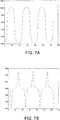
- Fig. 7A shows an example custom periodic phase signal.
- Fig. 7B shows the demodulated phase signal at the FBR output after delay through the power amplifier and other front-end components (e.g. duplexer filters, etc.).
- the recorded signal in Fig. 7B is the baseband phase signal result of the sum of the signal in Fig. 7A with a delayed version of itself.
- Fig. 8 shows an example of RF delay FOM measured based on the custom signal shown in Fig. 7A .
- the distance between points A and B may be used as an FOM to define the time mismatch (i.e. the RF delay) between the two signals.
- Points A and B may be defined as the intersection of the phase signal with a horizontal asymptote 802/804 at a fixed distance C from the average phase 806.
- This FOM offers advantages. It is easy to calculate. For example, 128 samples would be enough to record 3 to 6 values of FOM and obtain an average delay out of them.
- the FBR noise has a low impact and the calculated delay may be averaged in one FBR RAM reading operation.
- the transmitter e.g. a processor
- the transmitter may determine control parameters for DPD, adaptive ET, iterative transmit feedback loop (ITFL), or the like based on the comparison between time aligned signals of the transmitted signal and the feedback signal.
- IFL iterative transmit feedback loop
- Fig. 9 shows the relationship between the RF delay and the FOM calculated in accordance with the example shown in Fig. 8 . As shown in Fig. 9 , there is a good correlation between the FOM calculated in accordance with this example and the RF delay.
- Figs. 10A and 10B show comparison of the RF delay results obtained with the conventional method and the example method disclosed herein for the Bands 1 and 39 (as an example of the Long Term Evolution (LTE) bands), respectively. As shown in Figs. 10A and 10B , with the example methods disclosed herein it is possible to obtain a precise estimation of the RF delay in all the duplexer band.
- LTE Long Term Evolution
- Fig. 11 illustrates a user device 1100 (e.g. a UE) in accordance with an aspect.
- the user device 1100 may be a mobile device in some aspects and includes an application processor 1105, baseband processor 1110 (also referred to as a baseband module), radio front end module (RFEM) 1115, memory 1120, connectivity module 1125, near field communication (NFC) controller 1130, audio driver 1135, camera driver 1140, touch screen 1145, display driver 1150, sensors 1155, removable memory 1160, power management integrated circuit (PMIC) 1165 and smart battery 1170.
- application processor 1105 includes an application processor 1105, baseband processor 1110 (also referred to as a baseband module), radio front end module (RFEM) 1115, memory 1120, connectivity module 1125, near field communication (NFC) controller 1130, audio driver 1135, camera driver 1140, touch screen 1145, display driver 1150, sensors 1155, removable memory 1160, power management integrated circuit (PMIC) 1165 and smart battery 1170.
- application processor 1105 may include, for example, one or more CPU cores and one or more of cache memory, low drop-out voltage regulators (LDOs), interrupt controllers, serial interfaces such as serial peripheral interface (SPI), inter-integrated circuit (I 2 C) or universal programmable serial interface module, real time clock (RTC), timer-counters including interval and watchdog timers, general purpose input-output (IO), memory card controllers such as secure digital / multi-media card (SD/MMC) or similar, universal serial bus (USB) interfaces, mobile industry processor interface (MIPI) interfaces and Joint Test Access Group (JTAG) test access ports.
- LDOs low drop-out voltage regulators
- interrupt controllers serial interfaces such as serial peripheral interface (SPI), inter-integrated circuit (I 2 C) or universal programmable serial interface module, real time clock (RTC), timer-counters including interval and watchdog timers, general purpose input-output (IO), memory card controllers such as secure digital / multi-media card (SD/M
- baseband module 1110 may be implemented, for example, as a solder-down substrate including one or more integrated circuits, a single packaged integrated circuit soldered to a main circuit board, and/or a multi-chip module containing two or more integrated circuits.
- a computer program having a program code for performing at least one of the methods described herein, when the computer program is executed on a computer, a processor, or a programmable hardware component.
- a machine-readable storage including machine readable instructions, when executed, to implement a method or realize an apparatus as described herein.
- a further example is a machine-readable medium including code, when executed, to cause a machine to perform any of the methods described herein.
- Examples may further be or relate to a computer program having a program code for performing one or more of the above methods, when the computer program is executed on a computer or processor. Steps, operations or processes of various above-described methods may be performed by programmed computers or processors. Examples may also cover program storage devices such as digital data storage media, which are machine, processor or computer readable and encode machine-executable, processor-executable or computer-executable programs of instructions. The instructions perform or cause performing some or all of the acts of the above-described methods.
- the program storage devices may comprise or be, for instance, digital memories, magnetic storage media such as magnetic disks and magnetic tapes, hard drives, or optically readable digital data storage media.
- FIG. 1 may also cover computers, processors or control units programmed to perform the acts of the above-described methods or (field) programmable logic arrays ((F)PLAs) or (field) programmable gate arrays ((F)PGAs), programmed to perform the acts of the above-described methods.
- a functional block denoted as "means for " performing a certain function may refer to a circuit that is configured to perform a certain function.
- a "means for s.th.” may be implemented as a "means configured to or suited for s.th.”, such as a device or a circuit configured to or suited for the respective task.
- Functions of various elements shown in the figures may be implemented in the form of dedicated hardware, such as “a signal provider”, “a signal processing unit”, “a processor”, “a controller”, etc. as well as hardware capable of executing software in association with appropriate software.
- a processor the functions may be provided by a single dedicated processor, by a single shared processor, or by a plurality of individual processors, some of which or all of which may be shared.
- processor or “controller” is by far not limited to hardware exclusively capable of executing software but may include digital signal processor (DSP) hardware, network processor, application specific integrated circuit (ASIC), field programmable gate array (FPGA), read only memory (ROM) for storing software, random access memory (RAM), and non-volatile storage.
- DSP digital signal processor
- ASIC application specific integrated circuit
- FPGA field programmable gate array
- ROM read only memory
- RAM random access memory
- non-volatile storage Other hardware, conventional and/or custom, may also be included.
- a block diagram may, for instance, illustrate a high-level circuit diagram implementing the principles of the disclosure.
- a flow chart, a flow diagram, a state transition diagram, a pseudo code, and the like may represent various processes, operations or steps, which may, for instance, be substantially represented in computer readable medium and so executed by a computer or processor, whether or not such computer or processor is explicitly shown.
- Methods disclosed in the specification or in the claims may be implemented by a device having means for performing each of the respective acts of these methods.
- each claim may stand on its own as a separate example. While each claim may stand on its own as a separate example, it is to be noted that - although a dependent claim may refer in the claims to a specific combination with one or more other claims - other examples may also include a combination of the dependent claim with the subject matter of each other dependent or independent claim. Such combinations are explicitly proposed herein unless it is stated that a specific combination is not intended. Furthermore, it is intended to include also features of a claim to any other independent claim even if this claim is not directly made dependent to the independent claim.
Landscapes
- Engineering & Computer Science (AREA)
- Computer Networks & Wireless Communication (AREA)
- Signal Processing (AREA)
- Physics & Mathematics (AREA)
- Electromagnetism (AREA)
- Transmitters (AREA)
Abstract
Description
- Examples relate to estimation of front-end delay in a transmitter, more particularly, to a method and apparatus for calculating a radio frequency delay caused by front-end components based on measurements of a figure of merit in a transmitter system.
- Linearization techniques such as envelope tracking (ET) and digital pre-distortion (DPD) are nowadays widely used to improve the transmitter performance. A proper implementation of the linearization techniques requires a precise knowledge of the front-end distortions which cause degradation of the transmitted signal linearity. The front-end distortions (usually expressed in terms of amplitude vs amplitude (AM/AM) and amplitude vs difference between input and output phases - (AM/PM) characteristics) are usually calculated by aligning the baseband amplitude (AM) and phase (PM) signals before and after the front-end components of a transmitter. This operation assumes a higher degree of complexity on transmitter systems, due to the high precision required.
-
Fig. 1 shows a conventional polar transmitter with a feedback loop. Thephase component 104 of a transmit signal is modulated with a local oscillator (LO) signal and anamplitude component 102 of the transmit signal is modulated with the phase-modulatedLO signal 106. The modulatedtransmit signal 108 is then amplified by a power amplifier (PA) 110 and processed through front-end components 112, and then transmitted via anantenna 116. The transmit signal is tapped off by acoupler 114 and fed back to a receiver 120 (referred to hereinafter as a feedback receiver (FBR)). The phase-modulatedLO signal 106 is also forwarded to theFBR 120 and mixed with thefeedback signal 118 at the FBR 120. The FBR 120 recovers the amplitude component and the phase component from the feedback signal after mixing. - The
total time delay 130 to align the signal at the transmitter (TX) input with the demodulated transmitted signal is given by the sum of a baseband delay (BBDly) 132 and an analog radio frequency (RF) delay (RFDly) 134. Thebaseband delay 132 may be constant and is dependent on the digital components. TheRF delay 134 may be variable and may be caused by thepower amplifier 110 and other RF front-end components 112. The characterization of the two delay components is needed while aligning the transmitted and received phase signals (the PM_TX signal and the PM_FBR signal) since an advanced polar transmitter utilizes the same phase locked loop (PLL) for both modulation and demodulation of the PM signals. - The
PM_FBR signal 122 that is output from the FBR 120 includes two main components. One component is given by the signal path flowing through all the front-end which presents the front-end distortions, and the other component is the modulatedPM_TX signal 106 by the PLL. A signal alignment requires the knowledge of both baseband and RF delays to correctly reconstruct the two components using the PM TX signal. -
Fig. 2 shows a conventional system for RF delay measurements. Conventional systems use a complexdelay alignment block 200 to calculate the two delay components. In the conventional solution, the first step is to create a PM FBR-like signal 216 by adding the phase component of the transmit signal (PM_TX) 104 with a delayed version 212 (RF delay) of itself and adding abaseband delay 214. This may be done in the delay block 210. Theresulting signal 216 may then be compared to theoutput 122 of the FBR (PM_FBR) to calculate the baseband and RF delays. While the baseband delay is calculated offline by using time-consuming register-transfer level (RTL) hardware simulations, thedelay alignment block 200 performs an estimation of the RF delay by implementing a hardware optimization algorithm based on minimizing the variance between the modifiedPM_TX signal 216 and thePM_FBR signal 122. This may be done during calibration since the RF delay needs to be calculated for each frequency point. To calculate it, a sweep between different RF delay values is done in the delay block 210 until the difference between the two input signals is minimized. The hardware calculation result is a figure of merit (FOM) which describes the remaining variance between the two signals once alignment is performed. A low value of the FOM indicates a good correlation between the signals, and therefore a good time alignment. - This conventional solution presents the following disadvantages. A proper time alignment is based on two variables: the baseband delay and the RF delay. A pre-simulation needs to be done to find the optimum baseband delay values for each radio access technology (RAT) and consequently reduce the degree of freedom of the minimization algorithm. In addition, the delay estimation is done using noise-like signals. Therefore, the results of the FOM are strongly dependent on the signal itself and cannot be directly compared from iteration to iteration. An average value over 8 iterations is estimated to have a comparable FOM result, requiring around 0.5 ms with the current hardware implementation.
- Some examples of apparatuses and/or methods will be described in the following by way of example only, and with reference to the accompanying figures, in which
-
Fig. 1 shows a conventional polar transmitter with a feedback loop; -
Fig. 2 shows a conventional polar system for RF delay measurements; -
Fig. 3 shows a structure of an example transmitter including an RF delay measurement capability in accordance with one example; -
Fig. 4A shows a structure of an example I/Q transmitter including an RF delay measurement capability in accordance with one example; -
Fig. 4B shows a structure of an example polar transmitter including an RF delay measurement capability in accordance with one example; -
Fig. 5A shows a periodic trapezoidal phase signal as an example of the custom phase signal; -
Fig. 5B shows the received phase signals of the periodic trapezoidal phase signal ofFig. 5A with different delays; -
Fig. 5C shows the relation between the delay and the delta phase of the received PM signal; -
Figs. 6A and 6B show another example of figure of merit that may be used in calculating the RF delay and the relation between the FOM and the delay, respectively. -
Fig. 7A shows an example custom periodic phase signal; -
Fig. 7B shows the demodulated phase signal at the FBR output after delay through the power amplifier and other front-end components; -
Fig. 8 shows an example of RF delay FOM measured based on the custom signal shown inFig. 7A ; -
Fig. 9 shows the relationship between the RF delay and the FOM calculated in accordance with the example shown inFig. 8 ; -
Figs. 10A and 10B show comparison of the RF delay results obtained with the conventional method and the example method disclosed herein for theBands 1 and 39, respectively; and -
Fig. 11 illustrates a user device in accordance with an aspect. - Various examples will now be described more fully with reference to the accompanying drawings in which some examples are illustrated. In the figures, the thicknesses of lines, layers and/or regions may be exaggerated for clarity.
- Accordingly, while further examples are capable of various modifications and alternative forms, some particular examples thereof are shown in the figures and will subsequently be described in detail. However, this detailed description does not limit further examples to the particular forms described. Further examples may cover all modifications, equivalents, and alternatives falling within the scope of the disclosure. Like numbers refer to like or similar elements throughout the description of the figures, which may be implemented identically or in modified form when compared to one another while providing for the same or a similar functionality.
- It will be understood that when an element is referred to as being "connected" or "coupled" to another element, the elements may be directly connected or coupled or via one or more intervening elements. If two elements A and B are combined using an "or", this is to be understood to disclose all possible combinations, i.e. only A, only B as well as A and B. An alternative wording for the same combinations is "at least one of A and B". The same applies for combinations of more than 2 elements.
- The terminology used herein for the purpose of describing particular examples is not intended to be limiting for further examples. Whenever a singular form such as "a," "an" and "the" is used and using only a single element is neither explicitly or implicitly defined as being mandatory, further examples may also use plural elements to implement the same functionality. Likewise, when a functionality is subsequently described as being implemented using multiple elements, further examples may implement the same functionality using a single element or processing entity. It will be further understood that the terms "comprises," "comprising," "includes" and/or "including," when used, specify the presence of the stated features, integers, steps, operations, processes, acts, elements and/or components, but do not preclude the presence or addition of one or more other features, integers, steps, operations, processes, acts, elements, components and/or any group thereof.
- Unless otherwise defined, all terms (including technical and scientific terms) are used herein in their ordinary meaning of the art to which the examples belong.
- Examples are disclosed for simplified methods and apparatus to estimate the RF delay caused by front-end components in a transmitter based on measurements of particular phase characteristics of a customized signal. The examples are applicable to both a polar transmitter and an in-phase/quadrature (I/Q) transmitter.
-
Fig. 3 shows a structure of anexample transmitter 300 including an RF delay measurement capability in accordance with one example. Thetransmitter 300 includes a transmit circuitry, a coupler, a receive circuitry, and a delay measurement unit. The transmit circuitry including amodulator 306, apower amplifier 312, and other front-end components 314 is configured to modulate a local oscillator signal with a custom phase signal and transmit the modulated signal (i.e. the custom signal is upconverted using the LO signal). Thecoupler 316 is configured to couple the transmitted signal as a feedback signal. The receive circuitry including afeedback receiver 320 is configured to mix the feedback signal with the local oscillator signal modulated with a phase component of the custom phase signal and demodulate the mixed signal to extract a phase component of the feedback signal. Thedelay measurement unit 330 is configured to calculate a figure of merit using the phase component of themixed signal 326 and calculate an RF delay based on the figure of merit. - The
transmitter 300 may receive a transmit signal in the form of in-phase (I) and quadrature (Q)components 302/304 or alternatively in the form of polar symbols. The transmit signal is modulated by amodulator 306 with alocal oscillator signal 308. Themodulator 306 may be a polar modulator or an I/Q modulator. The modulated transmitsignal 310 may be represented as follows: INRF=AM(t)×sin(ωt+PM(t)). The modulated transmitsignal 310 is then processed by RF front-end components including aPA 312 and other front-end components 314, (e.g. filters, etc.). The transmit signal is then transmitted via anantenna 318. The transmitted signal is tapped off by acoupler 316 and fed back to a receiver (i.e. an FBR) 320 as a feedback signal. The tapped signal may be represented as follows: OUTRF=AM(t+TRF)×sin(ωt+PM(t+TRF)), where TRF is the RF front-end delay. It should be noted that the architecture of thetransmitters Figs. 3 ,4A and4B are just an example, and the position of the elements of thetransmitter power amplifier 312, the front-end components 314, and thecoupler 316 may be arranged differently (e.g. the front-end component 314 and thecoupler 316 may be switched). In this case the delay calculated is the delay inserted by thePA 312. - The
FBR 320 also receives a phase-modulated RF signal 322 (a modulated LO signal by a phase component of the transmit signal (i.e. the custom phase signal)) from themodulator 306. The phase-modulated RF signal may be represented as follows: PM_RF=sin(ωt+PM(t)). TheFBR 320 mixes the phase-modulated LO signal with thefeedback signal 324 to demodulate thefeedback signal 324 and recovers a phase component after mixing. The LO signal modulated with the phase component of the custom phase signal is used to demodulate the feedback signal. The recoveredphase component 326 from the mixed signal may be represented as follows: PM_FBR=PM(t) + PM(t+TRF)). The RFdelay measurement block 330 calculates a figure of merit which is directly related to the RF delay from thephase component 326 and calculates an RF delay based on the figure of merit. -
Fig. 4A shows a structure of an example I/Q transmitter 400 including an RF delay measurement capability in accordance with one example. The I andQ components 402/404 of the transmit signal are modulated by an I/Q modulator 406 with alocal oscillator signal 408. The modulated transmitsignal 410 is then processed by RF front-end components including a PA 412 and other front-end components 414, (e.g. filters, etc.) and transmitted via anantenna 418. The transmitted signal is tapped off by acoupler 416 and fed back to anFBR 420 as a feedback signal. - The I/
Q components 402/404 of the transmit signal may be converted to anamplitude component 424 and aphase component 426 by a coordinate rotation digital computer (CORDIC) 422 (or any coordinate conversion device). The LO signal is modulated with thephase component 426 of the transmit signal and the phase-modulated RF signal 428 (a modulated LO signal by a phase component of the transmit signal) is sent to theFBR 420. - The
FBR 420 mixes the phase-modulatedRF signal 428 and thefeedback signal 429 to demodulate thefeedback signal 429 and recovers a phase component after mixing. The RFdelay measurement block 430 calculates a figure of merit which is directly related to the RF delay from the recovered phase component and calculates an RF delay based on the figure of merit. -
Fig. 4B shows a structure of an examplepolar transmitter 450 including an RF delay measurement capability in accordance with one example. The I/Q components 452/454 of the transmit signal may be converted to anamplitude component 458 and aphase component 460 by a CORDIC 456 (or any coordinate conversion device). TheLO signal 462 is modulated with thephase component 460 of the transmit signal and theamplitude component 458 of the transmit signal is then modulated with the phase-modulatedLO signal 464 by thepolar modulator 466. The modulated transmitsignal 468 is then processed by RF front-end components including aPA 470 and other front-end components 472, (e.g. filters, etc.) and transmitted via anantenna 476. The transmitted signal is tapped off by acoupler 474 and fed back to anFBR 480 as afeedback signal 479. The phase-modulated RF signal 464 (a modulated LO signal by a phase component of the transmit signal) is sent to theFBR 480. - The
FBR 480 mixes the phase-modulatedRF signal 464 and thefeedback signal 479 to demodulate thefeedback signal 479 and recovers a phase component after mixing. The RF delay measurement block 490 calculates a figure of merit which is directly related to the RF delay from the recovered phase component and calculates an RF delay based on the figure of merit. - In examples, a custom phase signal which shows particular phase characteristics is used to measure the RF delay. The LO signal is modulated with the custom phase signal and the modulated LO signal is transmitted through the transmit chain. The phase-modulated LO signal (the LO signal modulated with the phase component of the custom phase signal) is also fed into the
FBR FBR coupler delay measurement block - In the examples, as shown in
Figs. 3 ,4A , and4B , no signal path is required from the phase component of the transmit signal (PM_TX) to thedelay measurement block - In one example, the custom phase signal may have a constant envelope and a trapezoidal periodic phase.
Fig. 5A shows a periodic trapezoidal phase signal as an example of the custom phase signal.Fig. 5B shows the received phase signals (PM_FBR) of the periodic trapezoidal phase signal ofFig. 5A with different delays (delays 1 - 5 in this example), which are obtained by demodulation of the feedback signal in theFBR - The demodulated PM signal by the
FBR Fig. 5B , the resulting phase signals for different time delays are plotted (expressed as sample delay inFig. 5B , therefore independent from the sampling rate of the signal itself). As shown inFig. 5B , the delta phase (e.g. defined as the maximum phase minus the minimum phase) increases as the RF delay increases fromdelay 1 to delay 5.Fig. 5C shows the relation between the delay (in samples) and the delta phase of the received PM signal (PM_FBR). A direct and precise relation between the delta phase and the delay mismatch (i.e. the RF delay) may be constructed, and the delta phase may be measured as an FOM and the RF delay may be estimated from the measured delta phase. -
Figs. 6A and 6B show another example of figure of merit that may be used in calculating the RF delay and the relation between the FOM and the delay, respectively. In this example, the figure of merit may be built taking into account the time that the received phase signal is zero or negative during one period. In this case, it may be directly related to the delay samples as shown inFig. 6B . - The figure of merits disclosed above and below are merely provided as examples, and any other forms of figure of merits may be used.
- In another example, a custom periodic phase signal may be used. The custom phase signal may present a constant envelope and a custom phase.
Fig. 7A shows an example custom periodic phase signal.Fig. 7B shows the demodulated phase signal at the FBR output after delay through the power amplifier and other front-end components (e.g. duplexer filters, etc.). The recorded signal inFig. 7B is the baseband phase signal result of the sum of the signal inFig. 7A with a delayed version of itself. -
Fig. 8 shows an example of RF delay FOM measured based on the custom signal shown inFig. 7A . For example, the distance between points A and B may be used as an FOM to define the time mismatch (i.e. the RF delay) between the two signals. Points A and B may be defined as the intersection of the phase signal with ahorizontal asymptote 802/804 at a fixed distance C from theaverage phase 806. - This FOM offers advantages. It is easy to calculate. For example, 128 samples would be enough to record 3 to 6 values of FOM and obtain an average delay out of them. The FBR noise has a low impact and the calculated delay may be averaged in one FBR RAM reading operation.
- After calculation of the RF delay, the transmitter (e.g. a processor) may determine control parameters for DPD, adaptive ET, iterative transmit feedback loop (ITFL), or the like based on the comparison between time aligned signals of the transmitted signal and the feedback signal. It should be noted that the custom phase signals and the FOMs shown in
Figs. 5A-8 are merely examples and any other custom phase signals and FOMs may be defined. -
Fig. 9 shows the relationship between the RF delay and the FOM calculated in accordance with the example shown inFig. 8 . As shown inFig. 9 , there is a good correlation between the FOM calculated in accordance with this example and the RF delay. -
Figs. 10A and 10B show comparison of the RF delay results obtained with the conventional method and the example method disclosed herein for theBands 1 and 39 (as an example of the Long Term Evolution (LTE) bands), respectively. As shown inFigs. 10A and 10B , with the example methods disclosed herein it is possible to obtain a precise estimation of the RF delay in all the duplexer band. -
Fig. 11 illustrates a user device 1100 (e.g. a UE) in accordance with an aspect. Theuser device 1100 may be a mobile device in some aspects and includes anapplication processor 1105, baseband processor 1110 (also referred to as a baseband module), radio front end module (RFEM) 1115,memory 1120,connectivity module 1125, near field communication (NFC)controller 1130,audio driver 1135,camera driver 1140,touch screen 1145,display driver 1150,sensors 1155,removable memory 1160, power management integrated circuit (PMIC) 1165 andsmart battery 1170. - In some aspects,
application processor 1105 may include, for example, one or more CPU cores and one or more of cache memory, low drop-out voltage regulators (LDOs), interrupt controllers, serial interfaces such as serial peripheral interface (SPI), inter-integrated circuit (I2C) or universal programmable serial interface module, real time clock (RTC), timer-counters including interval and watchdog timers, general purpose input-output (IO), memory card controllers such as secure digital / multi-media card (SD/MMC) or similar, universal serial bus (USB) interfaces, mobile industry processor interface (MIPI) interfaces and Joint Test Access Group (JTAG) test access ports. - In some aspects,
baseband module 1110 may be implemented, for example, as a solder-down substrate including one or more integrated circuits, a single packaged integrated circuit soldered to a main circuit board, and/or a multi-chip module containing two or more integrated circuits. Another example is a computer program having a program code for performing at least one of the methods described herein, when the computer program is executed on a computer, a processor, or a programmable hardware component. Another example is a machine-readable storage including machine readable instructions, when executed, to implement a method or realize an apparatus as described herein. A further example is a machine-readable medium including code, when executed, to cause a machine to perform any of the methods described herein. - The examples as described herein may be summarized as follows:
- Example 1 is a transmitter for calculating a radio frequency delay caused by front-end components in a transmitter. The transmitter comprises a transmit circuitry configured to modulate a local oscillator signal with a custom phase signal and transmit the modulated signal, a coupler configured to couple the transmitted signal as a feedback signal, a receive circuitry configured to mix the feedback signal with the local oscillator signal modulated with a phase of the custom phase signal and demodulate the mixed signal to extract a phase component from the mixed signal, and a delay measurement unit configured to calculate a figure of merit using the phase component of the mixed signal and calculate an RF delay based on the figure of merit.
- Example 2 is the transmitter of example 1, wherein the custom phase signal is a trapezoidal phase signal.
- Example 3 is the transmitter of example 2, wherein the figure of merit is a delta phase defined as a maximum phase minus a minimum phase.
- Example 4 is the transmitter of example 1, wherein the custom phase signal is a periodic phase signal.
- Example 5 is the transmitter of example 4, wherein the figure of merit is a distance between points of intersection of a phase signal with a horizontal asymptote at a fixed distance from an average phase.
- Example 6 is the transmitter as in any one of examples 1-5, wherein the transmitter is either a polar transmitter or an in-phase/quadrature transmitter.
- Example 7 is the transmitter as in any one of examples 1-6, further comprising a processor configured to determine control parameters for DPD, ET, and/or ITFL based on the RF delay.
- Example 8 is a method for calculating a radio frequency delay caused by front-end components in a transmitter. The method comprises generating a custom phase signal, modulating a local oscillator signal with the custom phase signal, transmitting the modulated signal via a transmit chain including the front-end components, coupling the transmitted signal to a receiver as a feedback signal, mixing the feedback signal with the local oscillator signal modulated with a phase of the custom phase signal; demodulating the mixed signal to extract a phase component from the mixed signal, calculating a figure of merit using the phase component of the mixed signal, and calculating an RF delay from the figure of merit.
- Example 9 is the method of example 8, wherein the custom phase signal is a trapezoidal phase signal.
- Example 10 is the method of example 9, wherein the figure of merit is a delta phase defined as a maximum phase minus a minimum phase.
- Example 11 is the method of example 8, wherein the custom phase signal is a periodic phase signal.
- Example 12 is the method of example 11, wherein the figure of merit is a distance between points of intersection of a phase signal with a horizontal asymptote at a fixed distance from an average phase.
- Example 13 is the method as in any one of examples 8-12, wherein the transmitter is either a polar transmitter or an in-phase/quadrature transmitter.
- Example 14 is the method as in any one of examples 8-13, further comprising determining control parameters for DPD, ET, and/or ITFL based on the RF delay.
- Example 15 is a machine-readable medium including code, when executed, to cause a machine to perform a method as in any one of examples 8-14.
- Example 16 is a transmitter for calculating a radio frequency delay caused by front-end components in a transmitter. The transmitter comprises a means for modulating a local oscillator signal with a custom phase signal and transmit the modulated signal, a means for coupling the transmitted signal as a feedback signal, a means for mixing the feedback signal with the local oscillator signal modulated with a phase of the custom phase signal and demodulating the mixed signal to extract a phase component from the mixed signal, and a means for calculating a figure of merit using the phase component of the mixed signal and calculating an RF delay based on the figure of merit.
- Example 17 is the transmitter of example 16, wherein the custom phase signal is a trapezoidal phase signal.
- Example 18 is the transmitter of example 17, wherein the figure of merit is a delta phase defined as a maximum phase minus a minimum phase.
- Example 19 is the transmitter of example 16, wherein the custom phase signal is a periodic phase signal.
- Example 20 is the transmitter of example 19, wherein the figure of merit is a distance between points of intersection of a phase signal with a horizontal asymptote at a fixed distance from an average phase.
- Example 21 is the transmitter as in any one of examples 16-20, wherein the transmitter is either a polar transmitter or an in-phase/quadrature transmitter.
- Example 22 is the transmitter as in any one of examples 16-21, further comprising a means for determining control parameters for DPD, ET, and/or ITFL based on the RF delay.
- Example 23 is a machine-readable storage including machine readable instructions, when executed, to implement a method or realize an apparatus as in any of examples 1-23.
- The aspects and features mentioned and described together with one or more of the previously detailed examples and figures, may as well be combined with one or more of the other examples in order to replace a like feature of the other example or in order to additionally introduce the feature to the other example.
- Examples may further be or relate to a computer program having a program code for performing one or more of the above methods, when the computer program is executed on a computer or processor. Steps, operations or processes of various above-described methods may be performed by programmed computers or processors. Examples may also cover program storage devices such as digital data storage media, which are machine, processor or computer readable and encode machine-executable, processor-executable or computer-executable programs of instructions. The instructions perform or cause performing some or all of the acts of the above-described methods. The program storage devices may comprise or be, for instance, digital memories, magnetic storage media such as magnetic disks and magnetic tapes, hard drives, or optically readable digital data storage media. Further examples may also cover computers, processors or control units programmed to perform the acts of the above-described methods or (field) programmable logic arrays ((F)PLAs) or (field) programmable gate arrays ((F)PGAs), programmed to perform the acts of the above-described methods.
- The description and drawings merely illustrate the principles of the disclosure. Furthermore, all examples recited herein are principally intended expressly to be only for pedagogical purposes to aid the reader in understanding the principles of the disclosure and the concepts contributed by the inventor(s) to furthering the art. All statements herein reciting principles, aspects, and examples of the disclosure, as well as specific examples thereof, are intended to encompass equivalents thereof.
- A functional block denoted as "means for ..." performing a certain function may refer to a circuit that is configured to perform a certain function. Hence, a "means for s.th." may be implemented as a "means configured to or suited for s.th.", such as a device or a circuit configured to or suited for the respective task.
- Functions of various elements shown in the figures, including any functional blocks labeled as "means", "means for providing a sensor signal", "means for generating a transmit signal.", etc., may be implemented in the form of dedicated hardware, such as "a signal provider", "a signal processing unit", "a processor", "a controller", etc. as well as hardware capable of executing software in association with appropriate software. When provided by a processor, the functions may be provided by a single dedicated processor, by a single shared processor, or by a plurality of individual processors, some of which or all of which may be shared. However, the term "processor" or "controller" is by far not limited to hardware exclusively capable of executing software but may include digital signal processor (DSP) hardware, network processor, application specific integrated circuit (ASIC), field programmable gate array (FPGA), read only memory (ROM) for storing software, random access memory (RAM), and non-volatile storage. Other hardware, conventional and/or custom, may also be included.
- A block diagram may, for instance, illustrate a high-level circuit diagram implementing the principles of the disclosure. Similarly, a flow chart, a flow diagram, a state transition diagram, a pseudo code, and the like may represent various processes, operations or steps, which may, for instance, be substantially represented in computer readable medium and so executed by a computer or processor, whether or not such computer or processor is explicitly shown. Methods disclosed in the specification or in the claims may be implemented by a device having means for performing each of the respective acts of these methods.
- It is to be understood that the disclosure of multiple acts, processes, operations, steps or functions disclosed in the specification or claims may not be construed as to be within the specific order, unless explicitly or implicitly stated otherwise, for instance for technical reasons. Therefore, the disclosure of multiple acts or functions will not limit these to a particular order unless such acts or functions are not interchangeable for technical reasons. Furthermore, in some examples a single act, function, process, operation or step may include or may be broken into multiple sub-acts, -functions, -processes, -operations or -steps, respectively. Such sub acts may be included and part of the disclosure of this single act unless explicitly excluded.
- Furthermore, the following claims are hereby incorporated into the detailed description, where each claim may stand on its own as a separate example. While each claim may stand on its own as a separate example, it is to be noted that - although a dependent claim may refer in the claims to a specific combination with one or more other claims - other examples may also include a combination of the dependent claim with the subject matter of each other dependent or independent claim. Such combinations are explicitly proposed herein unless it is stated that a specific combination is not intended. Furthermore, it is intended to include also features of a claim to any other independent claim even if this claim is not directly made dependent to the independent claim.
Claims (15)
- A transmitter for calculating a radio frequency, RF, delay caused by front-end components (312, 314) in a transmitter, the transmitter comprising:a transmit circuitry (306, 406, 466) configured to modulate a local oscillator signal with a custom phase signal and transmit the modulated signal;a coupler (316, 416, 476) configured to couple the transmitted signal as a feedback signal;a receive circuitry (320, 420, 480) configured to mix the feedback signal with the local oscillator signal modulated with a phase of the custom phase signal and demodulate the mixed signal to extract a phase component from the mixed signal; anda delay measurement unit (330, 430, 490) configured to calculate a figure of merit using the phase component of the mixed signal and calculate an RF delay based on the figure of merit.
- The transmitter of claim 1, wherein the custom phase signal is a trapezoidal phase signal.
- The transmitter of claim 2, wherein the figure of merit is a delta phase defined as a maximum phase minus a minimum phase.
- The transmitter of claim 1, wherein the custom phase signal is a periodic phase signal.
- The transmitter of claim 4, wherein the figure of merit is a distance between points of intersection of a phase signal with a horizontal asymptote at a fixed distance from an average phase.
- The transmitter as in any one of claims 1-5, wherein the transmitter is either a polar transmitter or an in-phase/quadrature transmitter.
- The transmitter as in any one of claims 1-6, further comprising:
a processor configured to determine control parameters for digital pre-distortion, DPD, envelop tracking, ET, and/or iterative transmit feedback loop, ITFL, based on the RF delay. - A method for calculating a radio frequency, RF, delay caused by front-end components in a transmitter, the method comprising:generating a custom phase signal;modulating a local oscillator signal with the custom phase signal;transmitting the modulated signal via a transmit chain including the front-end components;coupling the transmitted signal to a receiver as a feedback signal;mixing the feedback signal with the local oscillator signal modulated with a phase of the custom phase signal;demodulating the mixed signal to extract a phase component from the mixed signal;calculating a figure of merit using the phase component of the mixed signal; andcalculating an RF delay from the figure of merit.
- The method of claim 8, wherein the custom phase signal is a trapezoidal phase signal.
- The method of claim 9, wherein the figure of merit is a delta phase defined as a maximum phase minus a minimum phase.
- The method of claim 8, wherein the custom phase signal is a periodic phase signal.
- The method of claim 11, wherein the figure of merit is a distance between points of intersection of a phase signal with a horizontal asymptote at a fixed distance from an average phase.
- The method as in any one of claims 8-12, wherein the transmitter is either a polar transmitter or an in-phase/quadrature transmitter.
- The method as in any one of claims 8-13, further comprising:
determining control parameters for digital pre-distortion, DPD, envelop tracking, ET, and/or iterative transmit feedback loop, ITFL, based on the RF delay. - A machine-readable medium including code, when executed, to cause a machine to perform a method as in any one of claims 8-14.
Priority Applications (1)
| Application Number | Priority Date | Filing Date | Title |
|---|---|---|---|
| EP18180995.5A EP3588787B1 (en) | 2018-06-29 | 2018-06-29 | Method and apparatus for calculating a radio frequency delay caused by front-end components in a transmitter |
Applications Claiming Priority (1)
| Application Number | Priority Date | Filing Date | Title |
|---|---|---|---|
| EP18180995.5A EP3588787B1 (en) | 2018-06-29 | 2018-06-29 | Method and apparatus for calculating a radio frequency delay caused by front-end components in a transmitter |
Publications (2)
| Publication Number | Publication Date |
|---|---|
| EP3588787A1 true EP3588787A1 (en) | 2020-01-01 |
| EP3588787B1 EP3588787B1 (en) | 2021-04-28 |
Family
ID=62837823
Family Applications (1)
| Application Number | Title | Priority Date | Filing Date |
|---|---|---|---|
| EP18180995.5A Active EP3588787B1 (en) | 2018-06-29 | 2018-06-29 | Method and apparatus for calculating a radio frequency delay caused by front-end components in a transmitter |
Country Status (1)
| Country | Link |
|---|---|
| EP (1) | EP3588787B1 (en) |
Citations (4)
| Publication number | Priority date | Publication date | Assignee | Title |
|---|---|---|---|---|
| US20070009062A1 (en) * | 2004-11-17 | 2007-01-11 | Toru Matsuura | Transmitter circuit, transmission method, and communications device using the transmitter circuit |
| US20090096499A1 (en) * | 2007-10-10 | 2009-04-16 | Samsung Electronics Co., Ltd. | Apparatus and method for power amplification with delay control in wireless communication system |
| US20100105341A1 (en) * | 2008-10-27 | 2010-04-29 | Mediatek Inc. | Transmitter and control method for transmitting and calibrating a phase signal and an amplitude signal |
| US9867155B1 (en) * | 2016-09-19 | 2018-01-09 | Intel IP Corporation | Amplitude-modulation signal and phase-modulation signal delay adjustment for polar transmitter |
-
2018
- 2018-06-29 EP EP18180995.5A patent/EP3588787B1/en active Active
Patent Citations (4)
| Publication number | Priority date | Publication date | Assignee | Title |
|---|---|---|---|---|
| US20070009062A1 (en) * | 2004-11-17 | 2007-01-11 | Toru Matsuura | Transmitter circuit, transmission method, and communications device using the transmitter circuit |
| US20090096499A1 (en) * | 2007-10-10 | 2009-04-16 | Samsung Electronics Co., Ltd. | Apparatus and method for power amplification with delay control in wireless communication system |
| US20100105341A1 (en) * | 2008-10-27 | 2010-04-29 | Mediatek Inc. | Transmitter and control method for transmitting and calibrating a phase signal and an amplitude signal |
| US9867155B1 (en) * | 2016-09-19 | 2018-01-09 | Intel IP Corporation | Amplitude-modulation signal and phase-modulation signal delay adjustment for polar transmitter |
Also Published As
| Publication number | Publication date |
|---|---|
| EP3588787B1 (en) | 2021-04-28 |
Similar Documents
| Publication | Publication Date | Title |
|---|---|---|
| CN109428631B (en) | System for calibrating phase using system information | |
| US11223376B2 (en) | Frequency dependent envelope tracking | |
| EP2779472B1 (en) | A transmitter lo leakage calibration scheme using loopback circuitry | |
| TWI551038B (en) | Apparatus and method for amplitude modulation to phase modulation (ampm) distortion compensation | |
| CN103905128B (en) | There is signal delay estimator and the method for absolute delay amount and direction estimation | |
| TWI530134B (en) | Communication device for generating in-phase/orthogonal imbalance correction data and related non-transitory computer readable storage medium | |
| CN103748794A (en) | Rugged IQ receiver based RF gain measurements | |
| CN112213745A (en) | GPU-Based Satellite Slotting Receiver Processor Simulator | |
| CN103650604A (en) | Time delay estimation | |
| CN112291173A (en) | IQ imbalance coefficient acquisition method and device and readable storage medium | |
| CN101170537B (en) | Method and apparatus for compensating mismatch of radio frequency orthogonal receiver-transmitter | |
| CN108156103B (en) | IQ signal calibration method and device | |
| CN107547458B (en) | Method, device and remote radio unit for setting image suppression parameters in IQ modulation | |
| US9634694B2 (en) | Transmitter with a reduced complexity digital up-converter | |
| CN108449742A (en) | An auxiliary demodulation system and method for near field communication | |
| EP3588787A1 (en) | Method and apparatus for calculating a radio frequency delay caused by front-end components in a transmitter | |
| CN104483682B (en) | S-band unified TT&C system and its sidetone extraction module and range tone retransmission method | |
| CN102986140A (en) | Clocking scheme for a wireless communication device | |
| CN108649993A (en) | Whether there is or not communication signal transmissions delay measurement systems when plasma for one kind | |
| CN113973035A (en) | Transmitter and method for generating radio frequency transmission signal, mobile device and base station | |
| US8867399B2 (en) | Signal measurement | |
| WO2017210846A1 (en) | Method for suppressing local oscillator leakage in microwave chip and device thereof | |
| CN115902960A (en) | Receiving frequency calibration method, device, equipment, medium and product | |
| US20250112649A1 (en) | Transmitter and method to generate a transmit signal | |
| US20250105999A1 (en) | Contactless communication device by active load modulation |
Legal Events
| Date | Code | Title | Description |
|---|---|---|---|
| PUAI | Public reference made under article 153(3) epc to a published international application that has entered the european phase |
Free format text: ORIGINAL CODE: 0009012 |
|
| STAA | Information on the status of an ep patent application or granted ep patent |
Free format text: STATUS: THE APPLICATION HAS BEEN PUBLISHED |
|
| AK | Designated contracting states |
Kind code of ref document: A1 Designated state(s): AL AT BE BG CH CY CZ DE DK EE ES FI FR GB GR HR HU IE IS IT LI LT LU LV MC MK MT NL NO PL PT RO RS SE SI SK SM TR |
|
| AX | Request for extension of the european patent |
Extension state: BA ME |
|
| STAA | Information on the status of an ep patent application or granted ep patent |
Free format text: STATUS: REQUEST FOR EXAMINATION WAS MADE |
|
| 17P | Request for examination filed |
Effective date: 20200701 |
|
| RBV | Designated contracting states (corrected) |
Designated state(s): AL AT BE BG CH CY CZ DE DK EE ES FI FR GB GR HR HU IE IS IT LI LT LU LV MC MK MT NL NO PL PT RO RS SE SI SK SM TR |
|
| GRAP | Despatch of communication of intention to grant a patent |
Free format text: ORIGINAL CODE: EPIDOSNIGR1 |
|
| STAA | Information on the status of an ep patent application or granted ep patent |
Free format text: STATUS: GRANT OF PATENT IS INTENDED |
|
| RAP1 | Party data changed (applicant data changed or rights of an application transferred) |
Owner name: APPLE INC. |
|
| INTG | Intention to grant announced |
Effective date: 20201202 |
|
| GRAS | Grant fee paid |
Free format text: ORIGINAL CODE: EPIDOSNIGR3 |
|
| GRAA | (expected) grant |
Free format text: ORIGINAL CODE: 0009210 |
|
| STAA | Information on the status of an ep patent application or granted ep patent |
Free format text: STATUS: THE PATENT HAS BEEN GRANTED |
|
| AK | Designated contracting states |
Kind code of ref document: B1 Designated state(s): AL AT BE BG CH CY CZ DE DK EE ES FI FR GB GR HR HU IE IS IT LI LT LU LV MC MK MT NL NO PL PT RO RS SE SI SK SM TR |
|
| REG | Reference to a national code |
Ref country code: GB Ref legal event code: FG4D |
|
| REG | Reference to a national code |
Ref country code: CH Ref legal event code: EP |
|
| REG | Reference to a national code |
Ref country code: AT Ref legal event code: REF Ref document number: 1388313 Country of ref document: AT Kind code of ref document: T Effective date: 20210515 |
|
| REG | Reference to a national code |
Ref country code: DE Ref legal event code: R096 Ref document number: 602018016084 Country of ref document: DE |
|
| REG | Reference to a national code |
Ref country code: IE Ref legal event code: FG4D |
|
| REG | Reference to a national code |
Ref country code: LT Ref legal event code: MG9D |
|
| REG | Reference to a national code |
Ref country code: AT Ref legal event code: MK05 Ref document number: 1388313 Country of ref document: AT Kind code of ref document: T Effective date: 20210428 |
|
| PG25 | Lapsed in a contracting state [announced via postgrant information from national office to epo] |
Ref country code: HR Free format text: LAPSE BECAUSE OF FAILURE TO SUBMIT A TRANSLATION OF THE DESCRIPTION OR TO PAY THE FEE WITHIN THE PRESCRIBED TIME-LIMIT Effective date: 20210428 Ref country code: LT Free format text: LAPSE BECAUSE OF FAILURE TO SUBMIT A TRANSLATION OF THE DESCRIPTION OR TO PAY THE FEE WITHIN THE PRESCRIBED TIME-LIMIT Effective date: 20210428 Ref country code: FI Free format text: LAPSE BECAUSE OF FAILURE TO SUBMIT A TRANSLATION OF THE DESCRIPTION OR TO PAY THE FEE WITHIN THE PRESCRIBED TIME-LIMIT Effective date: 20210428 Ref country code: NL Free format text: LAPSE BECAUSE OF FAILURE TO SUBMIT A TRANSLATION OF THE DESCRIPTION OR TO PAY THE FEE WITHIN THE PRESCRIBED TIME-LIMIT Effective date: 20210428 Ref country code: AT Free format text: LAPSE BECAUSE OF FAILURE TO SUBMIT A TRANSLATION OF THE DESCRIPTION OR TO PAY THE FEE WITHIN THE PRESCRIBED TIME-LIMIT Effective date: 20210428 Ref country code: BG Free format text: LAPSE BECAUSE OF FAILURE TO SUBMIT A TRANSLATION OF THE DESCRIPTION OR TO PAY THE FEE WITHIN THE PRESCRIBED TIME-LIMIT Effective date: 20210728 |
|
| PG25 | Lapsed in a contracting state [announced via postgrant information from national office to epo] |
Ref country code: PT Free format text: LAPSE BECAUSE OF FAILURE TO SUBMIT A TRANSLATION OF THE DESCRIPTION OR TO PAY THE FEE WITHIN THE PRESCRIBED TIME-LIMIT Effective date: 20210830 Ref country code: PL Free format text: LAPSE BECAUSE OF FAILURE TO SUBMIT A TRANSLATION OF THE DESCRIPTION OR TO PAY THE FEE WITHIN THE PRESCRIBED TIME-LIMIT Effective date: 20210428 Ref country code: NO Free format text: LAPSE BECAUSE OF FAILURE TO SUBMIT A TRANSLATION OF THE DESCRIPTION OR TO PAY THE FEE WITHIN THE PRESCRIBED TIME-LIMIT Effective date: 20210728 Ref country code: LV Free format text: LAPSE BECAUSE OF FAILURE TO SUBMIT A TRANSLATION OF THE DESCRIPTION OR TO PAY THE FEE WITHIN THE PRESCRIBED TIME-LIMIT Effective date: 20210428 Ref country code: SE Free format text: LAPSE BECAUSE OF FAILURE TO SUBMIT A TRANSLATION OF THE DESCRIPTION OR TO PAY THE FEE WITHIN THE PRESCRIBED TIME-LIMIT Effective date: 20210428 Ref country code: RS Free format text: LAPSE BECAUSE OF FAILURE TO SUBMIT A TRANSLATION OF THE DESCRIPTION OR TO PAY THE FEE WITHIN THE PRESCRIBED TIME-LIMIT Effective date: 20210428 Ref country code: GR Free format text: LAPSE BECAUSE OF FAILURE TO SUBMIT A TRANSLATION OF THE DESCRIPTION OR TO PAY THE FEE WITHIN THE PRESCRIBED TIME-LIMIT Effective date: 20210729 Ref country code: IS Free format text: LAPSE BECAUSE OF FAILURE TO SUBMIT A TRANSLATION OF THE DESCRIPTION OR TO PAY THE FEE WITHIN THE PRESCRIBED TIME-LIMIT Effective date: 20210828 |
|
| REG | Reference to a national code |
Ref country code: NL Ref legal event code: MP Effective date: 20210428 |
|
| PG25 | Lapsed in a contracting state [announced via postgrant information from national office to epo] |
Ref country code: SM Free format text: LAPSE BECAUSE OF FAILURE TO SUBMIT A TRANSLATION OF THE DESCRIPTION OR TO PAY THE FEE WITHIN THE PRESCRIBED TIME-LIMIT Effective date: 20210428 Ref country code: SK Free format text: LAPSE BECAUSE OF FAILURE TO SUBMIT A TRANSLATION OF THE DESCRIPTION OR TO PAY THE FEE WITHIN THE PRESCRIBED TIME-LIMIT Effective date: 20210428 Ref country code: ES Free format text: LAPSE BECAUSE OF FAILURE TO SUBMIT A TRANSLATION OF THE DESCRIPTION OR TO PAY THE FEE WITHIN THE PRESCRIBED TIME-LIMIT Effective date: 20210428 Ref country code: EE Free format text: LAPSE BECAUSE OF FAILURE TO SUBMIT A TRANSLATION OF THE DESCRIPTION OR TO PAY THE FEE WITHIN THE PRESCRIBED TIME-LIMIT Effective date: 20210428 Ref country code: RO Free format text: LAPSE BECAUSE OF FAILURE TO SUBMIT A TRANSLATION OF THE DESCRIPTION OR TO PAY THE FEE WITHIN THE PRESCRIBED TIME-LIMIT Effective date: 20210428 Ref country code: DK Free format text: LAPSE BECAUSE OF FAILURE TO SUBMIT A TRANSLATION OF THE DESCRIPTION OR TO PAY THE FEE WITHIN THE PRESCRIBED TIME-LIMIT Effective date: 20210428 Ref country code: CZ Free format text: LAPSE BECAUSE OF FAILURE TO SUBMIT A TRANSLATION OF THE DESCRIPTION OR TO PAY THE FEE WITHIN THE PRESCRIBED TIME-LIMIT Effective date: 20210428 Ref country code: MC Free format text: LAPSE BECAUSE OF FAILURE TO SUBMIT A TRANSLATION OF THE DESCRIPTION OR TO PAY THE FEE WITHIN THE PRESCRIBED TIME-LIMIT Effective date: 20210428 |
|
| REG | Reference to a national code |
Ref country code: DE Ref legal event code: R097 Ref document number: 602018016084 Country of ref document: DE Ref country code: CH Ref legal event code: PL |
|
| PLBE | No opposition filed within time limit |
Free format text: ORIGINAL CODE: 0009261 |
|
| STAA | Information on the status of an ep patent application or granted ep patent |
Free format text: STATUS: NO OPPOSITION FILED WITHIN TIME LIMIT |
|
| REG | Reference to a national code |
Ref country code: BE Ref legal event code: MM Effective date: 20210630 |
|
| PG25 | Lapsed in a contracting state [announced via postgrant information from national office to epo] |
Ref country code: LU Free format text: LAPSE BECAUSE OF NON-PAYMENT OF DUE FEES Effective date: 20210629 |
|
| 26N | No opposition filed |
Effective date: 20220131 |
|
| PG25 | Lapsed in a contracting state [announced via postgrant information from national office to epo] |
Ref country code: LI Free format text: LAPSE BECAUSE OF NON-PAYMENT OF DUE FEES Effective date: 20210630 Ref country code: IE Free format text: LAPSE BECAUSE OF NON-PAYMENT OF DUE FEES Effective date: 20210629 Ref country code: CH Free format text: LAPSE BECAUSE OF NON-PAYMENT OF DUE FEES Effective date: 20210630 |
|
| PG25 | Lapsed in a contracting state [announced via postgrant information from national office to epo] |
Ref country code: IS Free format text: LAPSE BECAUSE OF FAILURE TO SUBMIT A TRANSLATION OF THE DESCRIPTION OR TO PAY THE FEE WITHIN THE PRESCRIBED TIME-LIMIT Effective date: 20210828 Ref country code: FR Free format text: LAPSE BECAUSE OF NON-PAYMENT OF DUE FEES Effective date: 20210630 Ref country code: AL Free format text: LAPSE BECAUSE OF FAILURE TO SUBMIT A TRANSLATION OF THE DESCRIPTION OR TO PAY THE FEE WITHIN THE PRESCRIBED TIME-LIMIT Effective date: 20210428 |
|
| PG25 | Lapsed in a contracting state [announced via postgrant information from national office to epo] |
Ref country code: IT Free format text: LAPSE BECAUSE OF FAILURE TO SUBMIT A TRANSLATION OF THE DESCRIPTION OR TO PAY THE FEE WITHIN THE PRESCRIBED TIME-LIMIT Effective date: 20210428 Ref country code: BE Free format text: LAPSE BECAUSE OF NON-PAYMENT OF DUE FEES Effective date: 20210630 |
|
| GBPC | Gb: european patent ceased through non-payment of renewal fee |
Effective date: 20220629 |
|
| PG25 | Lapsed in a contracting state [announced via postgrant information from national office to epo] |
Ref country code: GB Free format text: LAPSE BECAUSE OF NON-PAYMENT OF DUE FEES Effective date: 20220629 |
|
| PG25 | Lapsed in a contracting state [announced via postgrant information from national office to epo] |
Ref country code: CY Free format text: LAPSE BECAUSE OF FAILURE TO SUBMIT A TRANSLATION OF THE DESCRIPTION OR TO PAY THE FEE WITHIN THE PRESCRIBED TIME-LIMIT Effective date: 20210428 |
|
| PG25 | Lapsed in a contracting state [announced via postgrant information from national office to epo] |
Ref country code: HU Free format text: LAPSE BECAUSE OF FAILURE TO SUBMIT A TRANSLATION OF THE DESCRIPTION OR TO PAY THE FEE WITHIN THE PRESCRIBED TIME-LIMIT; INVALID AB INITIO Effective date: 20180629 |
|
| PG25 | Lapsed in a contracting state [announced via postgrant information from national office to epo] |
Ref country code: MK Free format text: LAPSE BECAUSE OF FAILURE TO SUBMIT A TRANSLATION OF THE DESCRIPTION OR TO PAY THE FEE WITHIN THE PRESCRIBED TIME-LIMIT Effective date: 20210428 |
|
| PG25 | Lapsed in a contracting state [announced via postgrant information from national office to epo] |
Ref country code: TR Free format text: LAPSE BECAUSE OF FAILURE TO SUBMIT A TRANSLATION OF THE DESCRIPTION OR TO PAY THE FEE WITHIN THE PRESCRIBED TIME-LIMIT Effective date: 20210428 |
|
| PG25 | Lapsed in a contracting state [announced via postgrant information from national office to epo] |
Ref country code: MT Free format text: LAPSE BECAUSE OF FAILURE TO SUBMIT A TRANSLATION OF THE DESCRIPTION OR TO PAY THE FEE WITHIN THE PRESCRIBED TIME-LIMIT Effective date: 20210428 |
|
| PGFP | Annual fee paid to national office [announced via postgrant information from national office to epo] |
Ref country code: DE Payment date: 20250402 Year of fee payment: 8 |