EP3586399B1 - Device for electromagnetically probing a sample - Google Patents
Device for electromagnetically probing a sample Download PDFInfo
- Publication number
- EP3586399B1 EP3586399B1 EP17713144.8A EP17713144A EP3586399B1 EP 3586399 B1 EP3586399 B1 EP 3586399B1 EP 17713144 A EP17713144 A EP 17713144A EP 3586399 B1 EP3586399 B1 EP 3586399B1
- Authority
- EP
- European Patent Office
- Prior art keywords
- circuit board
- metal body
- antenna
- antenna structure
- receiver
- Prior art date
- Legal status (The legal status is an assumption and is not a legal conclusion. Google has not performed a legal analysis and makes no representation as to the accuracy of the status listed.)
- Active
Links
Images


Classifications
-
- G—PHYSICS
- G01—MEASURING; TESTING
- G01S—RADIO DIRECTION-FINDING; RADIO NAVIGATION; DETERMINING DISTANCE OR VELOCITY BY USE OF RADIO WAVES; LOCATING OR PRESENCE-DETECTING BY USE OF THE REFLECTION OR RERADIATION OF RADIO WAVES; ANALOGOUS ARRANGEMENTS USING OTHER WAVES
- G01S7/00—Details of systems according to groups G01S13/00, G01S15/00, G01S17/00
- G01S7/02—Details of systems according to groups G01S13/00, G01S15/00, G01S17/00 of systems according to group G01S13/00
- G01S7/03—Details of HF subsystems specially adapted therefor, e.g. common to transmitter and receiver
-
- G—PHYSICS
- G01—MEASURING; TESTING
- G01S—RADIO DIRECTION-FINDING; RADIO NAVIGATION; DETERMINING DISTANCE OR VELOCITY BY USE OF RADIO WAVES; LOCATING OR PRESENCE-DETECTING BY USE OF THE REFLECTION OR RERADIATION OF RADIO WAVES; ANALOGOUS ARRANGEMENTS USING OTHER WAVES
- G01S13/00—Systems using the reflection or reradiation of radio waves, e.g. radar systems; Analogous systems using reflection or reradiation of waves whose nature or wavelength is irrelevant or unspecified
- G01S13/88—Radar or analogous systems specially adapted for specific applications
- G01S13/887—Radar or analogous systems specially adapted for specific applications for detection of concealed objects, e.g. contraband or weapons
-
- H—ELECTRICITY
- H01—ELECTRIC ELEMENTS
- H01Q—ANTENNAS, i.e. RADIO AERIALS
- H01Q1/00—Details of, or arrangements associated with, antennas
- H01Q1/52—Means for reducing coupling between antennas; Means for reducing coupling between an antenna and another structure
-
- G—PHYSICS
- G01—MEASURING; TESTING
- G01S—RADIO DIRECTION-FINDING; RADIO NAVIGATION; DETERMINING DISTANCE OR VELOCITY BY USE OF RADIO WAVES; LOCATING OR PRESENCE-DETECTING BY USE OF THE REFLECTION OR RERADIATION OF RADIO WAVES; ANALOGOUS ARRANGEMENTS USING OTHER WAVES
- G01S13/00—Systems using the reflection or reradiation of radio waves, e.g. radar systems; Analogous systems using reflection or reradiation of waves whose nature or wavelength is irrelevant or unspecified
- G01S13/88—Radar or analogous systems specially adapted for specific applications
-
- G—PHYSICS
- G01—MEASURING; TESTING
- G01S—RADIO DIRECTION-FINDING; RADIO NAVIGATION; DETERMINING DISTANCE OR VELOCITY BY USE OF RADIO WAVES; LOCATING OR PRESENCE-DETECTING BY USE OF THE REFLECTION OR RERADIATION OF RADIO WAVES; ANALOGOUS ARRANGEMENTS USING OTHER WAVES
- G01S7/00—Details of systems according to groups G01S13/00, G01S15/00, G01S17/00
- G01S7/02—Details of systems according to groups G01S13/00, G01S15/00, G01S17/00 of systems according to group G01S13/00
-
- H—ELECTRICITY
- H01—ELECTRIC ELEMENTS
- H01Q—ANTENNAS, i.e. RADIO AERIALS
- H01Q1/00—Details of, or arrangements associated with, antennas
- H01Q1/42—Housings not intimately mechanically associated with radiating elements, e.g. radome
-
- H—ELECTRICITY
- H01—ELECTRIC ELEMENTS
- H01Q—ANTENNAS, i.e. RADIO AERIALS
- H01Q1/00—Details of, or arrangements associated with, antennas
- H01Q1/52—Means for reducing coupling between antennas; Means for reducing coupling between an antenna and another structure
- H01Q1/521—Means for reducing coupling between antennas; Means for reducing coupling between an antenna and another structure reducing the coupling between adjacent antennas
- H01Q1/525—Means for reducing coupling between antennas; Means for reducing coupling between an antenna and another structure reducing the coupling between adjacent antennas between emitting and receiving antennas
-
- H—ELECTRICITY
- H01—ELECTRIC ELEMENTS
- H01Q—ANTENNAS, i.e. RADIO AERIALS
- H01Q1/00—Details of, or arrangements associated with, antennas
- H01Q1/52—Means for reducing coupling between antennas; Means for reducing coupling between an antenna and another structure
- H01Q1/526—Electromagnetic shields
-
- H—ELECTRICITY
- H01—ELECTRIC ELEMENTS
- H01Q—ANTENNAS, i.e. RADIO AERIALS
- H01Q17/00—Devices for absorbing waves radiated from an antenna; Combinations of such devices with active antenna elements or systems
- H01Q17/007—Devices for absorbing waves radiated from an antenna; Combinations of such devices with active antenna elements or systems with means for controlling the absorption
-
- G—PHYSICS
- G01—MEASURING; TESTING
- G01S—RADIO DIRECTION-FINDING; RADIO NAVIGATION; DETERMINING DISTANCE OR VELOCITY BY USE OF RADIO WAVES; LOCATING OR PRESENCE-DETECTING BY USE OF THE REFLECTION OR RERADIATION OF RADIO WAVES; ANALOGOUS ARRANGEMENTS USING OTHER WAVES
- G01S7/00—Details of systems according to groups G01S13/00, G01S15/00, G01S17/00
- G01S7/02—Details of systems according to groups G01S13/00, G01S15/00, G01S17/00 of systems according to group G01S13/00
- G01S7/027—Constructional details of housings, e.g. form, type, material or ruggedness
Definitions
- the invention relates to a device for the non-destructive probing of a sample, in particular a structure of concrete, by means of electromagnetic wave reflection.
- EP 2720065 describes a device of this type. It comprises a housing-like frame with four wheels. Electromagnetic waves are sent into the sample by means of an antenna structure. Echo signals reflected back from the sample are received by the antenna structure and analyzed.
- DE 10 2014 218 364 shows a mobile measuring apparatus for nondestructively determining a material measurement value that relates to a material property of a workpiece.
- the apparatus comprises a housing in which at least a first sensor device and a second sensor device are located, a control device, an evaluating device, and a device for the supply of energy to the measuring apparatus.
- the first sensor device has a nuclear magnetic resonance sensor and the second sensor device has a sensor based on dielectric and/or resistive methods.
- Information about the material property of the workpiece, in particular moisture present in the workpiece is obtained by evaluating a measurement signal provided by the first sensor device, which information is intended for the optimized control of the second sensor device and/or optimized evaluation of measurement signals provided by the second sensor device.
- the problem to be solved by the present invention is to provide a device of this type that is easy to construct.
- the device comprises:
- first circuit board is mounted to the first side of the metal body and the second circuit board is mounted to the second side of said circuit body.
- this design allows a simple mounting of both circuit boards to opposite sides of the metal body as a common carrier.
- the metal body forms a mount as well as a spacer between the two boards.
- the metal body comprises a lateral wall that circumferentially encloses an interior space, i.e. that surrounds the interior space on all sides with the possible exception of the sides of the first and second sides.
- the interior space is adjacent to the second side of the metal body, and the antenna structure is adjacent to the interior space.
- This design electrically shields the interior space and therefore the side of the antenna structure that faces away from the sample.
- the lateral wall extends laterally outside the antenna structure such that all of the antenna structure borders the interior space.
- the metal body can further comprise a separating wall closing the interior space towards the first side. This separating wall shields the antenna structure from the circuit board carrying the driver and receiver.
- the device can further comprise a damping structure, advantageously separate from the metal body, arranged in the interior space in order to absorb and thereby damp the waves emitted by the antenna structure into the metal body and to suppress reflections originating from that side.
- the damping structure can comprise a conductive foam.
- the metal body can further comprise a shielding structure that extends between the separating wall and the first circuit board. It forms several mutually shielded chambers between the separating wall and the first circuit board. This allows to shield different parts of the circuitry on the first circuit board from each other.
- circuitry of the driver and circuitry of the receiver are backed by different shielded chambers, i.e. separate shielded chambers are located between the driver and the receiver circuitry and the separating wall.
- the antenna structure comprises a sender antenna for sending the probe signal into the sample and a receiver antenna for receiving an echo of the probe signal reflected from the sample.
- the metal body advantageously comprises a shield wall that shields the receiver antenna from the sender antenna in order to reduce direct cross-talk between these antennas.
- the shield wall ends at the second circuit board, i.e. at the circuit board carrying the antenna structure.
- the shield wall extends between the second circuit board and the separating wall and divides said interior space into a first chamber backing the sender antenna and a second chamber backing the receiver antenna.
- backing is to be understood such that the respective chambers are located between the respective antennas and the separating wall.
- the connector can be plugged into the first and/or the second circuit board, thereby forming a releasable connection for easier assembly and disassembly.
- the present device can be used for probing the structure of any kind of sample, but it is advantageously used for probing the structure of concrete, e.g. of a building, tunnel or bridge.
- Fig. 1 shows a device for determining the structure of a sample by means of electromagnetic reflection measurements.
- It comprises a frame 2 forming a housing enclosing the electronic components of the device.
- the device comprises a set of wheels 4, in particular four wheels, by means of which the device can be guided along the sample at a defined distance therefrom.
- the device can e.g. also have only two or three wheels, or wheel-like components, such as rollers or sliders.
- the housing comprises, at a side opposite to the wheels 4, a handle 6 to be gripped by the user.
- the device also comprises input and output devices, such as a touchscreen 8.
- Fig. 2 shows some of the electronic components within the device. These include, by way of example, the following parts:
- control unit 24 In operation, the user typically moves the device along the sample while control unit 24 performs a stream of measurements.
- Control unit 24, or circuitry external to the device can use the recorded data in order to determine the sample's internal structure, e.g. using SAFT (Synthetic Aperture Focusing Technique) technology as it is known to the skilled person.
- SAFT Synthetic Aperture Focusing Technique
- a core of the device of Fig. 1 is formed by a metal body 30.
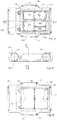
- This metal body can e.g. form the bottom side of frame 2. It is shown in Figs. 2 - 8 .
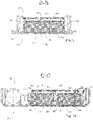
- Metal body 30 is advantageously a single piece of cast and/or worked metal, in particular aluminum. It comprises a first side 32 and a second side 34 ( Figs. 5 , 7, 8 ). In operation, first side 32 is facing away from the sample, while second side 34 is located on the side of frame 2 where the wheels 4 are mounted, i.e. second side 34 faces the sample to be measured.
- Metal body 30 comprises a base plate 36 ( Figs. 7, 8 ) at its second side 34. It forms a wall of frame 2 towards the sample.
- An opening 38 is arranged in base plate 36.
- metal body 30 On the side of base plate 36 that faces away from second side 34, metal body 30 forms a lateral wall 40 that extends around opening 38. Lateral wall 40 is advantageously aligned perpendicularly to base plate 36.
- Lateral wall 40 encloses, i.e. runs around, an interior space 42, 43.
- Metal body 30 further forms a separating wall 44. It extends parallel to, and at a distance from, base plate 36 and borders interior space 42, 43.
- Metal body 30 further forms a shield wall 45. It is perpendicular to base plate 36 and extends between two opposite sides of lateral wall 40, thereby dividing interior space 42, 43 into a first chamber 42 and a second chamber 43. Shield wall 45 extends between second side 34 (namely opening 38) and separating wall 44.
- metal body 30 forms a shielding structure 46a - 46e (see Figs. 3 , 4 , generally denoted by reference number 46 in the following) formed by a plurality of raised structures on the side of separating wall 44.
- Shielding structure 46 faces first side 32. It extends between separating wall 44 and first side 32 (i.e. between separating wall 44 and the first circuit board 54 mentioned below) and forms several, mutually shielded chambers 48a - 48e (which are, in the following generally denoted by reference number 48 and shown in Fig. 4 ).
- Metal body 30 further forms wheel holders 50 for holding bearings for the wheels 4 and therefore for holding the wheels 4.
- Base plate 36 extends between lateral wall 40 and the wheel holders 50, thereby connecting these parts.
- frame 2 of the device further comprises a cover 52 mounted to the second side of metal body 30 and forming an upper side of the device's housing.
- Handle 6 is mounted to cover 52 or forms a part thereof.
- metal body 30 is used for mounting two circuit boards 54, 56.
- a first circuit board 54 is attached to first side 32 of metal body 30, namely to shielding structure 46, e.g. by means of screws (sitting in screw openings some of which are denoted with reference number 58 in Fig. 4 ). Shielding structure 46 extends along the edge of first circuit board 54 thereby shielding it.
- a second circuit board 56 is attached to second side 34 of metal body 30, again e.g. by means of screws (sitting in screw openings, some of which are denoted with reference number 50 in Fig. 6 ). Second circuit board 56 is mounted over opening 38 ( Fig. 7, 8 ). Lateral wall 40 extends along the edge of second circuit board 56 thereby shielding it.
- First circuit board 54 holds at least part of the electronics of driver 10, 12 and/or of receiver 14, 16. Advantageously, it holds at least the analog parts 12 and 14 thereof.
- First circuit board 54 can be a multi-layer PCB comprising a shield layer 62 that provides radio frequency shielding to the components above it.
- a shield layer 62 that provides radio frequency shielding to the components above it.
- at least some of the electronic components of the sender 10, 12 and/or the receiver 14, 16 are on the side of shield layer 62 that faces second side 34 of metal body 30 in order to be shielded.
- Second circuit board 56 holds the two antennas 20, 22, which can e.g. be implemented as circular conductive regions or in a bow-tie arrangement structured in a conductive layer of second circuit board 56.
- Sender antenna 20 and receiver antenna 22 are on opposite sides of shield wall 45 in order to reduce cross-talk between them.
- the device further comprises a damping structure 58 arranged in interior space 42, 43, namely in first chamber 42 and second chamber 43.
- Damping structure 58 is an extended structure, advantageously separate from metal body 30. It is designed to absorb electromagnetic radiation (of the frequencies used by the device) without reflecting it.
- damping structure 58 can be a conductive foam, e.g. a foam comprising graphite.
- separating wall 44 is advantageously closer to first circuit board 54 than to second circuit board 56.
- antenna structure 18 i.e. both antennas 20, 22, is backed by interior space 42, 43 such that all the backside of antenna structure 18 is damped.
- first chamber 42 is arranged at the backside of antenna 20 and second chamber 43 is arranged at the backside of antenna 22.
- the antennas 20, 22 on second circuit board 56 have to be electrically connected to first circuit board 54.
- the present device is provided with at least one electrical connector 60 extending between first and second circuit boards 54, 56.
- this electrical connector is plugged into one or both of the circuit boards 54, 56.
- Each connector 60 is a rigid rod having a first plug 62 plugged into first circuit board 54 and/or a second plug 64 plugged into second circuit board 56.
- each connector extends perpendicularly to the circuit boards 54, 56.
- separating wall 44 For each connector 60, separating wall 44 comprises an opening 66 ( Figs. 4 and 6 ) with the connector 60 extending through it.
- each of the first and second circuit boards 54, 56 is formed by a single board, it is possible to assemble each of them from two or more boards, each such board only holding part of the circuitry and antenna structure, respectively.
- using single boards is advantageous because it makes it easier to assemble the device.
Landscapes
- Engineering & Computer Science (AREA)
- Radar, Positioning & Navigation (AREA)
- Remote Sensing (AREA)
- Physics & Mathematics (AREA)
- Computer Networks & Wireless Communication (AREA)
- General Physics & Mathematics (AREA)
- Electromagnetism (AREA)
- Shielding Devices Or Components To Electric Or Magnetic Fields (AREA)
- Emergency Protection Circuit Devices (AREA)
- Thermistors And Varistors (AREA)
Description
- The invention relates to a device for the non-destructive probing of a sample, in particular a structure of concrete, by means of electromagnetic wave reflection.
-
EP 2720065 describes a device of this type. It comprises a housing-like frame with four wheels. Electromagnetic waves are sent into the sample by means of an antenna structure. Echo signals reflected back from the sample are received by the antenna structure and analyzed. -
DE 10 2014 218 364 shows a mobile measuring apparatus for nondestructively determining a material measurement value that relates to a material property of a workpiece. The apparatus comprises a housing in which at least a first sensor device and a second sensor device are located, a control device, an evaluating device, and a device for the supply of energy to the measuring apparatus. The first sensor device has a nuclear magnetic resonance sensor and the second sensor device has a sensor based on dielectric and/or resistive methods. Information about the material property of the workpiece, in particular moisture present in the workpiece, is obtained by evaluating a measurement signal provided by the first sensor device, which information is intended for the optimized control of the second sensor device and/or optimized evaluation of measurement signals provided by the second sensor device. - The problem to be solved by the present invention is to provide a device of this type that is easy to construct.
- This problem is solved by the device of claim 1. Accordingly, the device comprises:
- A frame: This is the mechanical framework of the device.
- An antenna structure: This may be a single antenna acting as a sender and a receiver, or it may comprise two separate antennas for sending and receiving the signals, respectively.
- A driver: The driver comprises at least the output stage of the electronics generating the probe signal. It is electrically connected to the antenna structure for sending the probe signal through the same.
- A receiver: The receiver comprises at least the input stage of the electronics for receiving the echo signal. It is electrically connected to the antenna structure for receiving the echo signal through the same.
- At least a first circuit board: At least part of the driver and/or the receiver is arranged on this first circuit board.
- At least a second circuit board: The antenna structure is arranged on this second circuit board.
- A metal body: This metal body is arranged in the frame (by forming part of the frame or by being mounted to the frame). The metal body has first and second opposite sides.
- At least one electrical connector: This connects the two circuit boards.
- Further, the first circuit board is mounted to the first side of the metal body and the second circuit board is mounted to the second side of said circuit body.
- Hence, this design allows a simple mounting of both circuit boards to opposite sides of the metal body as a common carrier. The metal body forms a mount as well as a spacer between the two boards.
- The metal body comprises a lateral wall that circumferentially encloses an interior space, i.e. that surrounds the interior space on all sides with the possible exception of the sides of the first and second sides. The interior space is adjacent to the second side of the metal body, and the antenna structure is adjacent to the interior space. This design electrically shields the interior space and therefore the side of the antenna structure that faces away from the sample. Advantageously, the lateral wall extends laterally outside the antenna structure such that all of the antenna structure borders the interior space.
- The metal body can further comprise a separating wall closing the interior space towards the first side. This separating wall shields the antenna structure from the circuit board carrying the driver and receiver.
- The device can further comprise a damping structure, advantageously separate from the metal body, arranged in the interior space in order to absorb and thereby damp the waves emitted by the antenna structure into the metal body and to suppress reflections originating from that side. Advantageously, the damping structure can comprise a conductive foam.
- The metal body can further comprise a shielding structure that extends between the separating wall and the first circuit board. It forms several mutually shielded chambers between the separating wall and the first circuit board. This allows to shield different parts of the circuitry on the first circuit board from each other. In particular, circuitry of the driver and circuitry of the receiver are backed by different shielded chambers, i.e. separate shielded chambers are located between the driver and the receiver circuitry and the separating wall.
- In a further embodiment, the antenna structure comprises a sender antenna for sending the probe signal into the sample and a receiver antenna for receiving an echo of the probe signal reflected from the sample. In this case, the metal body advantageously comprises a shield wall that shields the receiver antenna from the sender antenna in order to reduce direct cross-talk between these antennas. The shield wall ends at the second circuit board, i.e. at the circuit board carrying the antenna structure.
- Advantageously, the shield wall extends between the second circuit board and the separating wall and divides said interior space into a first chamber backing the sender antenna and a second chamber backing the receiver antenna. In this context, "backing" is to be understood such that the respective chambers are located between the respective antennas and the separating wall.
- The connector can be plugged into the first and/or the second circuit board, thereby forming a releasable connection for easier assembly and disassembly.
- The present device can be used for probing the structure of any kind of sample, but it is advantageously used for probing the structure of concrete, e.g. of a building, tunnel or bridge.
- The invention will be better understood and objects other than those set forth above will become apparent when consideration is given to the following detailed description thereof. This description makes reference to the annexed drawings, wherein:
-
Fig. 1 shows a view of a device, -
Fig. 2 shows a block circuit diagram of the device, -
Fig. 3 shows a metal body to be used in the device, -
Fig. 4 is a view of the metal body from its first side, -
Fig. 5 is a side view of the metal body, -
Fig. 6 is a view of the metal body from its second side, -
Fig. 7 is a sectional view along line B-B ofFig. 5 , -
Fig. 8 is a sectional view along line C-C ofFig. 4 , -
Fig. 9 is the sectional view ofFig. 7 including some parts of the electronics and the damping structure, and -
Fig. 10 is the sectional view ofFig. 8 including some parts of the electronics and the damping structure. -
Fig. 1 shows a device for determining the structure of a sample by means of electromagnetic reflection measurements. - It comprises a
frame 2 forming a housing enclosing the electronic components of the device. - In the embodiment shown here, the device comprises a set of
wheels 4, in particular four wheels, by means of which the device can be guided along the sample at a defined distance therefrom. Instead of four wheels, the device can e.g. also have only two or three wheels, or wheel-like components, such as rollers or sliders. - Further, the housing comprises, at a side opposite to the
wheels 4, ahandle 6 to be gripped by the user. - The device also comprises input and output devices, such as a
touchscreen 8. -
Fig. 2 shows some of the electronic components within the device. These include, by way of example, the following parts: - A
driver Driver digital section 10 as well as ananalog section 12.Digital section 10 can e.g. be used to generate a pulse or a CW signal, andanalog section 12 can be used to amplify and/or modulate and/or filter this signal. - A
receiver analogue section 14 for filtering and/or demodulating and/or amplifying the received signal as well as adigital section 16 for further signal processing. - An
antenna structure 18 for sending the probe signal into the sample and for receiving the echo signal reflected therefrom. In the present embodiment,antenna structure 18 comprises asender antenna 20 and, separate from thesender antenna 20, areceiver antenna 22.Driver sender antenna 20 andreceiver receiver antenna 22. - A
control unit 24 for controlling the components in the device, for operatingscreen 8 and for communication with external circuitry. - In operation, the user typically moves the device along the sample while
control unit 24 performs a stream of measurements.Control unit 24, or circuitry external to the device, can use the recorded data in order to determine the sample's internal structure, e.g. using SAFT (Synthetic Aperture Focusing Technique) technology as it is known to the skilled person. - A core of the device of
Fig. 1 is formed by ametal body 30. This metal body can e.g. form the bottom side offrame 2. It is shown inFigs. 2 - 8 . -
Metal body 30 is advantageously a single piece of cast and/or worked metal, in particular aluminum. It comprises afirst side 32 and a second side 34 (Figs. 5 ,7, 8 ). In operation,first side 32 is facing away from the sample, whilesecond side 34 is located on the side offrame 2 where thewheels 4 are mounted, i.e.second side 34 faces the sample to be measured. -
Metal body 30 comprises a base plate 36 (Figs. 7, 8 ) at itssecond side 34. It forms a wall offrame 2 towards the sample. - An
opening 38 is arranged inbase plate 36. - On the side of
base plate 36 that faces away fromsecond side 34,metal body 30 forms alateral wall 40 that extends around opening 38.Lateral wall 40 is advantageously aligned perpendicularly tobase plate 36. -
Lateral wall 40 encloses, i.e. runs around, aninterior space -
Metal body 30 further forms a separatingwall 44. It extends parallel to, and at a distance from,base plate 36 and bordersinterior space -
Metal body 30 further forms ashield wall 45. It is perpendicular tobase plate 36 and extends between two opposite sides oflateral wall 40, thereby dividinginterior space first chamber 42 and asecond chamber 43.Shield wall 45 extends between second side 34 (namely opening 38) and separatingwall 44. - Further,
metal body 30 forms a shieldingstructure 46a - 46e (seeFigs. 3 ,4 , generally denoted by reference number 46 in the following) formed by a plurality of raised structures on the side of separatingwall 44. Shielding structure 46 facesfirst side 32. It extends between separatingwall 44 and first side 32 (i.e. between separatingwall 44 and thefirst circuit board 54 mentioned below) and forms several, mutually shieldedchambers 48a - 48e (which are, in the following generally denoted by reference number 48 and shown inFig. 4 ). -
Metal body 30 further forms wheelholders 50 for holding bearings for thewheels 4 and therefore for holding thewheels 4. -
Base plate 36 extends betweenlateral wall 40 and thewheel holders 50, thereby connecting these parts. - As shown in
Fig. 1 ,frame 2 of the device further comprises acover 52 mounted to the second side ofmetal body 30 and forming an upper side of the device's housing.Handle 6 is mounted to cover 52 or forms a part thereof. - As shown in
Figs. 9 and 10 ,metal body 30 is used for mounting twocircuit boards - A
first circuit board 54 is attached tofirst side 32 ofmetal body 30, namely to shielding structure 46, e.g. by means of screws (sitting in screw openings some of which are denoted withreference number 58 inFig. 4 ). Shielding structure 46 extends along the edge offirst circuit board 54 thereby shielding it. - A
second circuit board 56 is attached tosecond side 34 ofmetal body 30, again e.g. by means of screws (sitting in screw openings, some of which are denoted withreference number 50 inFig. 6 ).Second circuit board 56 is mounted over opening 38 (Fig. 7, 8 ).Lateral wall 40 extends along the edge ofsecond circuit board 56 thereby shielding it. -
First circuit board 54 holds at least part of the electronics ofdriver receiver analog parts -
First circuit board 54 can be a multi-layer PCB comprising ashield layer 62 that provides radio frequency shielding to the components above it. In this case, at least some of the electronic components of thesender receiver shield layer 62 that facessecond side 34 ofmetal body 30 in order to be shielded. - In order to avoid crosstalk, different parts of the circuitry on
first circuit board 54 are located in different ones of the shielded chambers 48. In particular, the circuitry of the driver and the circuitry of the receiver are backed by different ones of the shielded chambers 48. -
Second circuit board 56 holds the twoantennas second circuit board 56. -
Sender antenna 20 andreceiver antenna 22 are on opposite sides ofshield wall 45 in order to reduce cross-talk between them. - Further, and as shown in
Figs. 9 and 10 , the device further comprises a dampingstructure 58 arranged ininterior space first chamber 42 andsecond chamber 43. Dampingstructure 58 is an extended structure, advantageously separate frommetal body 30. It is designed to absorb electromagnetic radiation (of the frequencies used by the device) without reflecting it. For example, dampingstructure 58 can be a conductive foam, e.g. a foam comprising graphite. - In order to have a large volume available for damping
structure 58, separatingwall 44 is advantageously closer tofirst circuit board 54 than tosecond circuit board 56. - As mentioned, all of
antenna structure 18, i.e. bothantennas interior space antenna structure 18 is damped. - In the present case,
first chamber 42 is arranged at the backside ofantenna 20 andsecond chamber 43 is arranged at the backside ofantenna 22. - The
antennas second circuit board 56 have to be electrically connected tofirst circuit board 54. For this purpose, the present device is provided with at least oneelectrical connector 60 extending between first andsecond circuit boards circuit boards - In the embodiment of
Figs. 9 and 10 , there are twosuch connectors 60. Eachconnector 60 is a rigid rod having afirst plug 62 plugged intofirst circuit board 54 and/or asecond plug 64 plugged intosecond circuit board 56. - Advantageously, each connector extends perpendicularly to the
circuit boards - For each
connector 60, separatingwall 44 comprises an opening 66 (Figs. 4 and 6 ) with theconnector 60 extending through it. - Even though, in the present embodiment, each of the first and
second circuit boards - While there are shown and described presently preferred embodiments of the invention, it is to be distinctly understood that the invention is not limited thereto but may be otherwise variously embodied and practiced within the scope of the following claims.
Claims (16)
- A device for the non-destructive probing of a sample by means of electromagnetic wave reflection, said device comprising
a frame (2),
an antenna structure (20, 22),
a driver (10, 12) electrically connected to said antenna structure (20, 22) for sending a probe signal through said antenna structure (20, 22),
a receiver (14, 16) electrically connected to said antenna structure (20, 22) for receiving an echo signal through said antenna structure (20, 22),
at least a first circuit board (54), wherein at least part of said driver (10, 12) and/or said receiver (14, 16) is arranged on said first circuit board (54),
at least a second circuit board (56), wherein said antenna structure (20, 22) is arranged on said second circuit board (56),
a metal body (30) arranged in said frame (2) having first and second opposite sides,
at least one electrical connector (60) for electrically connecting said first and second circuit boards (54, 56),
wherein said first circuit board (54) is mounted to the first side of said metal body (30) and said second circuit board (56) is mounted to the second side of said circuit body,
wherein said metal body (30) comprises a lateral wall (40) circumferentially enclosing an interior space (42, 43) adjacent to said second side, wherein said antenna structure (18) is adjacent to said interior space (42, 43),
wherein said device further comprises a set of wheels (4) for rolling it along said sample, wherein said wheels (4) are mounted to said metal body (30),
wherein said metal body (30) comprises wheel holders (50) for holding said wheels (4) and
a base plate (36) at its second side and extending between said lateral wall (40) and said wheel holders (50),
and wherein said second circuit board (56) is arranged in an opening (38) of said base plate (36). - The device of claim 1 wherein the lateral wall (40) extends laterally outside the antenna structure (18) .
- The device of any of the preceding claims further comprising a damping structure (58) arranged in said interior space (42, 43), and in particular wherein said damping structure (58) is separate from said metal body (30).
- The device of claim 3 wherein said damping structure (58) comprises a conductive foam.
- The device of any of the preceding claims wherein said metal body (30) comprises a separating wall (44) closing said interior space (42, 43) towards said first side, and in particular wherein said separating wall (44) is closer to said first circuit board (54) than to said second circuit board (56).
- The device of claim 5 wherein said metal body (30) comprises a shielding structure (46) extending between said separating wall (44) and said first circuit board (54) and forming several mutually shielded chambers (48) between said separating wall (44) and said first circuit board (54).
- The device of claim 6 wherein circuitry of the driver (10, 12) and circuitry of the receiver (14, 16) are backed by different ones of said shielded chambers (48).
- The device of any of the preceding claims wherein said antenna structure (20, 22) comprises a sender antenna and a receiver antenna.
- The device of claim 8 wherein said metal body (30) comprises a shield wall (45) shielding said receiver antenna from said sender antenna, wherein said shield wall (45) ends at said second circuit board (56).
- The device of the claims 7 and 9 wherein said shield wall extends between said second circuit board (56) and said separating wall (44) dividing said interior space (42, 43) into a first chamber (42) backing said sender antenna (20) and a second chamber (43) backing said receiver antenna (22).
- The device of any of the preceding claims wherein said electrical connector (60) is a rigid rod having a first plug (62) plugged into said first circuit board (54) and/or a second plug (64) plugged into said second circuit board (56), and in particular wherein said device comprises at least two such electrical connectors (60) .
- The device of the claims 5 and 11 wherein said separating wall (44) comprises an opening (66) and wherein said connector (60) extends through said opening (66) .
- The device of any of the preceding claims wherein said connector (60) is plugged into said first and/or said second circuit board (54, 56).
- The device of any of the preceding claims wherein said first and/or said second circuit board (54, 56) is/are attached to said metal body (30).
- The device of any of the preceding claims wherein said metal body (30) is a single metal piece, in particular of aluminum.
- Use of the device of any of the preceding claims for probing the structure of concrete.
Priority Applications (1)
| Application Number | Priority Date | Filing Date | Title |
|---|---|---|---|
| PL17713144T PL3586399T3 (en) | 2017-03-10 | 2017-03-10 | Device for electromagnetically probing a sample |
Applications Claiming Priority (1)
| Application Number | Priority Date | Filing Date | Title |
|---|---|---|---|
| PCT/CH2017/000027 WO2018161182A1 (en) | 2017-03-10 | 2017-03-10 | Device for electromagnetically probing a sample |
Publications (2)
| Publication Number | Publication Date |
|---|---|
| EP3586399A1 EP3586399A1 (en) | 2020-01-01 |
| EP3586399B1 true EP3586399B1 (en) | 2021-03-31 |
Family
ID=58410052
Family Applications (1)
| Application Number | Title | Priority Date | Filing Date |
|---|---|---|---|
| EP17713144.8A Active EP3586399B1 (en) | 2017-03-10 | 2017-03-10 | Device for electromagnetically probing a sample |
Country Status (8)
| Country | Link |
|---|---|
| US (1) | US11543515B2 (en) |
| EP (1) | EP3586399B1 (en) |
| JP (1) | JP7021244B2 (en) |
| CA (1) | CA3055443C (en) |
| ES (1) | ES2865510T3 (en) |
| PL (1) | PL3586399T3 (en) |
| RU (1) | RU2725700C1 (en) |
| WO (1) | WO2018161182A1 (en) |
Families Citing this family (1)
| Publication number | Priority date | Publication date | Assignee | Title |
|---|---|---|---|---|
| CN110715706B (en) * | 2019-11-25 | 2021-08-13 | 重庆宇虹自动化仪表系统有限公司 | Portable sauce-flavored pottery altar nondestructive parameter detector |
Family Cites Families (12)
| Publication number | Priority date | Publication date | Assignee | Title |
|---|---|---|---|---|
| EP0349110B1 (en) * | 1988-05-27 | 1992-03-11 | British Gas plc | Ground probing radar method and apparatus |
| EP0995128A1 (en) * | 1997-07-02 | 2000-04-26 | Ekko Dane Production A/S | Radar plant and measurement technique for determination of the orientation and the depth of buried objects |
| WO2002063334A2 (en) * | 2001-02-03 | 2002-08-15 | Robert Bosch Gmbh | Integrated circuit for a radar device in a hermetically sealed housing comprising a patch antenna formed from a bent component from sheet metal |
| US7196655B1 (en) * | 2003-10-27 | 2007-03-27 | Atr Electronics, Inc. | System and method for highly directional electronic identification and communication and combat identification system employing the same |
| RU2282875C1 (en) * | 2005-03-03 | 2006-08-27 | Вячеслав Адамович Заренков | Building structure exploration device |
| US7518880B1 (en) * | 2006-02-08 | 2009-04-14 | Bi-Link | Shielding arrangement for electronic device |
| USD630268S1 (en) * | 2009-11-25 | 2011-01-04 | John Cunningham | Remote controlled vehicle |
| US9194950B2 (en) | 2012-01-19 | 2015-11-24 | Black & Decker Inc. | Handheld locating device |
| US9073347B2 (en) | 2012-10-11 | 2015-07-07 | Geophysical Survey Systems, Inc. | Hand-held radar device with direct printing based on radar input |
| DE102012111183A1 (en) * | 2012-11-20 | 2014-05-22 | Conti Temic Microelectronic Gmbh | Radar device for a vehicle |
| DE102014218364A1 (en) * | 2014-09-12 | 2016-03-17 | Robert Bosch Gmbh | Hand-held measuring device and method for its operation |
| US10074907B2 (en) | 2015-03-12 | 2018-09-11 | Veoneer Us, Inc. | Apparatus and method for mitigating multipath effects and improving absorption of an automotive radar module |
-
2017
- 2017-03-10 PL PL17713144T patent/PL3586399T3/en unknown
- 2017-03-10 ES ES17713144T patent/ES2865510T3/en active Active
- 2017-03-10 RU RU2019128236A patent/RU2725700C1/en active
- 2017-03-10 WO PCT/CH2017/000027 patent/WO2018161182A1/en not_active Ceased
- 2017-03-10 US US16/491,923 patent/US11543515B2/en active Active
- 2017-03-10 JP JP2019548896A patent/JP7021244B2/en active Active
- 2017-03-10 CA CA3055443A patent/CA3055443C/en active Active
- 2017-03-10 EP EP17713144.8A patent/EP3586399B1/en active Active
Non-Patent Citations (1)
| Title |
|---|
| None * |
Also Published As
| Publication number | Publication date |
|---|---|
| US11543515B2 (en) | 2023-01-03 |
| WO2018161182A1 (en) | 2018-09-13 |
| JP2020512687A (en) | 2020-04-23 |
| CA3055443C (en) | 2024-06-25 |
| US20210141081A1 (en) | 2021-05-13 |
| ES2865510T3 (en) | 2021-10-15 |
| JP7021244B2 (en) | 2022-02-16 |
| EP3586399A1 (en) | 2020-01-01 |
| PL3586399T3 (en) | 2021-09-06 |
| CA3055443A1 (en) | 2018-09-13 |
| RU2725700C1 (en) | 2020-07-03 |
Similar Documents
| Publication | Publication Date | Title |
|---|---|---|
| EP2002270B1 (en) | High performance miniature rf sensor for use in microelectronics plasma processing tools | |
| US6590391B1 (en) | Mri diagnosis apparatus with an intergrated cabinet that is mechanically and electrically connected to the electrically conductive shield of the shield room in which the mr measurement system is arranged | |
| US20110032162A1 (en) | Antenna testing device and antenna testing method using the same | |
| KR20160107222A (en) | Radiating structure with integrated proximity sensing | |
| CN110693497B (en) | Hybrid imaging device | |
| CN102175696A (en) | Method and device for measuring moisture of material | |
| JP4358512B2 (en) | Position measuring device | |
| US11543515B2 (en) | Device for electromagnetically probing a sample | |
| CN109782195B (en) | An Induction Coil Magnetic Field Measurement System Against Noise Interference | |
| CN210534025U (en) | Wave-absorbing material test fixture | |
| CN115128362B (en) | In-situ test device and test method for electromagnetic shielding effectiveness of optical window | |
| JP6379752B2 (en) | Quartz crystal resonator and crystal resonator characteristic measuring method | |
| CN206060773U (en) | A kind of shielded box with USB interface | |
| CN211880889U (en) | Electromagnetic shielding and seam angle measuring device of waveguide tube | |
| SE500305C2 (en) | Method and apparatus for measuring electromagnetic radiation from or reception of external electromagnetic radiation in a circuit board | |
| JP2008082945A (en) | Near electromagnetic field distribution measurement apparatus | |
| Van Helvoort et al. | Frequency-dependent shielding of electronics inside an MRI system | |
| Tong et al. | A novel strategy for high-performance underwater acoustic transducer design: acoustic impedance matching, shielding and on-chip amplification | |
| JPH0449586Y2 (en) | ||
| US5392256A (en) | Magneto-acoustic signal conditioner | |
| RU2256904C1 (en) | Radio introscopy device | |
| US20120050117A1 (en) | Electromagnetic interference test device | |
| JPS61126456A (en) | Detector for high-frequency magnetic field generation | |
| KR20240157364A (en) | Electromagnetic wave shielding performance evaluation device and evaluation method of electronic devices | |
| US7564399B2 (en) | Shielded compartment for mounting a high frequency radar component on a printed circuit board |
Legal Events
| Date | Code | Title | Description |
|---|---|---|---|
| STAA | Information on the status of an ep patent application or granted ep patent |
Free format text: STATUS: UNKNOWN |
|
| STAA | Information on the status of an ep patent application or granted ep patent |
Free format text: STATUS: THE INTERNATIONAL PUBLICATION HAS BEEN MADE |
|
| PUAI | Public reference made under article 153(3) epc to a published international application that has entered the european phase |
Free format text: ORIGINAL CODE: 0009012 |
|
| STAA | Information on the status of an ep patent application or granted ep patent |
Free format text: STATUS: REQUEST FOR EXAMINATION WAS MADE |
|
| 17P | Request for examination filed |
Effective date: 20190924 |
|
| AK | Designated contracting states |
Kind code of ref document: A1 Designated state(s): AL AT BE BG CH CY CZ DE DK EE ES FI FR GB GR HR HU IE IS IT LI LT LU LV MC MK MT NL NO PL PT RO RS SE SI SK SM TR |
|
| AX | Request for extension of the european patent |
Extension state: BA ME |
|
| DAV | Request for validation of the european patent (deleted) | ||
| DAX | Request for extension of the european patent (deleted) | ||
| GRAP | Despatch of communication of intention to grant a patent |
Free format text: ORIGINAL CODE: EPIDOSNIGR1 |
|
| STAA | Information on the status of an ep patent application or granted ep patent |
Free format text: STATUS: GRANT OF PATENT IS INTENDED |
|
| INTG | Intention to grant announced |
Effective date: 20201103 |
|
| GRAS | Grant fee paid |
Free format text: ORIGINAL CODE: EPIDOSNIGR3 |
|
| GRAA | (expected) grant |
Free format text: ORIGINAL CODE: 0009210 |
|
| STAA | Information on the status of an ep patent application or granted ep patent |
Free format text: STATUS: THE PATENT HAS BEEN GRANTED |
|
| AK | Designated contracting states |
Kind code of ref document: B1 Designated state(s): AL AT BE BG CH CY CZ DE DK EE ES FI FR GB GR HR HU IE IS IT LI LT LU LV MC MK MT NL NO PL PT RO RS SE SI SK SM TR |
|
| REG | Reference to a national code |
Ref country code: GB Ref legal event code: FG4D Ref country code: CH Ref legal event code: EP |
|
| REG | Reference to a national code |
Ref country code: DE Ref legal event code: R096 Ref document number: 602017035636 Country of ref document: DE Ref country code: CH Ref legal event code: NV Representative=s name: E. BLUM AND CO. AG PATENT- UND MARKENANWAELTE V, CH Ref country code: AT Ref legal event code: REF Ref document number: 1377978 Country of ref document: AT Kind code of ref document: T Effective date: 20210415 |
|
| REG | Reference to a national code |
Ref country code: NL Ref legal event code: FP |
|
| REG | Reference to a national code |
Ref country code: IE Ref legal event code: FG4D |
|
| REG | Reference to a national code |
Ref country code: LT Ref legal event code: MG9D |
|
| PG25 | Lapsed in a contracting state [announced via postgrant information from national office to epo] |
Ref country code: NO Free format text: LAPSE BECAUSE OF FAILURE TO SUBMIT A TRANSLATION OF THE DESCRIPTION OR TO PAY THE FEE WITHIN THE PRESCRIBED TIME-LIMIT Effective date: 20210630 Ref country code: HR Free format text: LAPSE BECAUSE OF FAILURE TO SUBMIT A TRANSLATION OF THE DESCRIPTION OR TO PAY THE FEE WITHIN THE PRESCRIBED TIME-LIMIT Effective date: 20210331 Ref country code: FI Free format text: LAPSE BECAUSE OF FAILURE TO SUBMIT A TRANSLATION OF THE DESCRIPTION OR TO PAY THE FEE WITHIN THE PRESCRIBED TIME-LIMIT Effective date: 20210331 Ref country code: BG Free format text: LAPSE BECAUSE OF FAILURE TO SUBMIT A TRANSLATION OF THE DESCRIPTION OR TO PAY THE FEE WITHIN THE PRESCRIBED TIME-LIMIT Effective date: 20210630 |
|
| PG25 | Lapsed in a contracting state [announced via postgrant information from national office to epo] |
Ref country code: RS Free format text: LAPSE BECAUSE OF FAILURE TO SUBMIT A TRANSLATION OF THE DESCRIPTION OR TO PAY THE FEE WITHIN THE PRESCRIBED TIME-LIMIT Effective date: 20210331 Ref country code: LV Free format text: LAPSE BECAUSE OF FAILURE TO SUBMIT A TRANSLATION OF THE DESCRIPTION OR TO PAY THE FEE WITHIN THE PRESCRIBED TIME-LIMIT Effective date: 20210331 Ref country code: SE Free format text: LAPSE BECAUSE OF FAILURE TO SUBMIT A TRANSLATION OF THE DESCRIPTION OR TO PAY THE FEE WITHIN THE PRESCRIBED TIME-LIMIT Effective date: 20210331 |
|
| REG | Reference to a national code |
Ref country code: AT Ref legal event code: MK05 Ref document number: 1377978 Country of ref document: AT Kind code of ref document: T Effective date: 20210331 |
|
| REG | Reference to a national code |
Ref country code: ES Ref legal event code: FG2A Ref document number: 2865510 Country of ref document: ES Kind code of ref document: T3 Effective date: 20211015 |
|
| PG25 | Lapsed in a contracting state [announced via postgrant information from national office to epo] |
Ref country code: LT Free format text: LAPSE BECAUSE OF FAILURE TO SUBMIT A TRANSLATION OF THE DESCRIPTION OR TO PAY THE FEE WITHIN THE PRESCRIBED TIME-LIMIT Effective date: 20210331 Ref country code: EE Free format text: LAPSE BECAUSE OF FAILURE TO SUBMIT A TRANSLATION OF THE DESCRIPTION OR TO PAY THE FEE WITHIN THE PRESCRIBED TIME-LIMIT Effective date: 20210331 Ref country code: CZ Free format text: LAPSE BECAUSE OF FAILURE TO SUBMIT A TRANSLATION OF THE DESCRIPTION OR TO PAY THE FEE WITHIN THE PRESCRIBED TIME-LIMIT Effective date: 20210331 Ref country code: SM Free format text: LAPSE BECAUSE OF FAILURE TO SUBMIT A TRANSLATION OF THE DESCRIPTION OR TO PAY THE FEE WITHIN THE PRESCRIBED TIME-LIMIT Effective date: 20210331 Ref country code: AT Free format text: LAPSE BECAUSE OF FAILURE TO SUBMIT A TRANSLATION OF THE DESCRIPTION OR TO PAY THE FEE WITHIN THE PRESCRIBED TIME-LIMIT Effective date: 20210331 |
|
| PG25 | Lapsed in a contracting state [announced via postgrant information from national office to epo] |
Ref country code: SK Free format text: LAPSE BECAUSE OF FAILURE TO SUBMIT A TRANSLATION OF THE DESCRIPTION OR TO PAY THE FEE WITHIN THE PRESCRIBED TIME-LIMIT Effective date: 20210331 Ref country code: RO Free format text: LAPSE BECAUSE OF FAILURE TO SUBMIT A TRANSLATION OF THE DESCRIPTION OR TO PAY THE FEE WITHIN THE PRESCRIBED TIME-LIMIT Effective date: 20210331 Ref country code: PT Free format text: LAPSE BECAUSE OF FAILURE TO SUBMIT A TRANSLATION OF THE DESCRIPTION OR TO PAY THE FEE WITHIN THE PRESCRIBED TIME-LIMIT Effective date: 20210802 Ref country code: IS Free format text: LAPSE BECAUSE OF FAILURE TO SUBMIT A TRANSLATION OF THE DESCRIPTION OR TO PAY THE FEE WITHIN THE PRESCRIBED TIME-LIMIT Effective date: 20210731 |
|
| REG | Reference to a national code |
Ref country code: DE Ref legal event code: R097 Ref document number: 602017035636 Country of ref document: DE |
|
| PG25 | Lapsed in a contracting state [announced via postgrant information from national office to epo] |
Ref country code: AL Free format text: LAPSE BECAUSE OF FAILURE TO SUBMIT A TRANSLATION OF THE DESCRIPTION OR TO PAY THE FEE WITHIN THE PRESCRIBED TIME-LIMIT Effective date: 20210331 Ref country code: DK Free format text: LAPSE BECAUSE OF FAILURE TO SUBMIT A TRANSLATION OF THE DESCRIPTION OR TO PAY THE FEE WITHIN THE PRESCRIBED TIME-LIMIT Effective date: 20210331 |
|
| PLBE | No opposition filed within time limit |
Free format text: ORIGINAL CODE: 0009261 |
|
| STAA | Information on the status of an ep patent application or granted ep patent |
Free format text: STATUS: NO OPPOSITION FILED WITHIN TIME LIMIT |
|
| 26N | No opposition filed |
Effective date: 20220104 |
|
| PG25 | Lapsed in a contracting state [announced via postgrant information from national office to epo] |
Ref country code: IS Free format text: LAPSE BECAUSE OF FAILURE TO SUBMIT A TRANSLATION OF THE DESCRIPTION OR TO PAY THE FEE WITHIN THE PRESCRIBED TIME-LIMIT Effective date: 20210731 |
|
| PG25 | Lapsed in a contracting state [announced via postgrant information from national office to epo] |
Ref country code: MC Free format text: LAPSE BECAUSE OF FAILURE TO SUBMIT A TRANSLATION OF THE DESCRIPTION OR TO PAY THE FEE WITHIN THE PRESCRIBED TIME-LIMIT Effective date: 20210331 |
|
| REG | Reference to a national code |
Ref country code: BE Ref legal event code: MM Effective date: 20220331 |
|
| PG25 | Lapsed in a contracting state [announced via postgrant information from national office to epo] |
Ref country code: LU Free format text: LAPSE BECAUSE OF NON-PAYMENT OF DUE FEES Effective date: 20220310 Ref country code: IE Free format text: LAPSE BECAUSE OF NON-PAYMENT OF DUE FEES Effective date: 20220310 |
|
| PG25 | Lapsed in a contracting state [announced via postgrant information from national office to epo] |
Ref country code: BE Free format text: LAPSE BECAUSE OF NON-PAYMENT OF DUE FEES Effective date: 20220331 |
|
| P01 | Opt-out of the competence of the unified patent court (upc) registered |
Effective date: 20230523 |
|
| PGFP | Annual fee paid to national office [announced via postgrant information from national office to epo] |
Ref country code: NL Payment date: 20240320 Year of fee payment: 8 |
|
| PG25 | Lapsed in a contracting state [announced via postgrant information from national office to epo] |
Ref country code: MK Free format text: LAPSE BECAUSE OF FAILURE TO SUBMIT A TRANSLATION OF THE DESCRIPTION OR TO PAY THE FEE WITHIN THE PRESCRIBED TIME-LIMIT Effective date: 20210331 Ref country code: CY Free format text: LAPSE BECAUSE OF FAILURE TO SUBMIT A TRANSLATION OF THE DESCRIPTION OR TO PAY THE FEE WITHIN THE PRESCRIBED TIME-LIMIT Effective date: 20210331 |
|
| PG25 | Lapsed in a contracting state [announced via postgrant information from national office to epo] |
Ref country code: HU Free format text: LAPSE BECAUSE OF FAILURE TO SUBMIT A TRANSLATION OF THE DESCRIPTION OR TO PAY THE FEE WITHIN THE PRESCRIBED TIME-LIMIT; INVALID AB INITIO Effective date: 20170310 |
|
| PGFP | Annual fee paid to national office [announced via postgrant information from national office to epo] |
Ref country code: PL Payment date: 20240229 Year of fee payment: 8 |
|
| PG25 | Lapsed in a contracting state [announced via postgrant information from national office to epo] |
Ref country code: TR Free format text: LAPSE BECAUSE OF FAILURE TO SUBMIT A TRANSLATION OF THE DESCRIPTION OR TO PAY THE FEE WITHIN THE PRESCRIBED TIME-LIMIT Effective date: 20210331 |
|
| PGFP | Annual fee paid to national office [announced via postgrant information from national office to epo] |
Ref country code: ES Payment date: 20240429 Year of fee payment: 8 |
|
| PG25 | Lapsed in a contracting state [announced via postgrant information from national office to epo] |
Ref country code: MT Free format text: LAPSE BECAUSE OF FAILURE TO SUBMIT A TRANSLATION OF THE DESCRIPTION OR TO PAY THE FEE WITHIN THE PRESCRIBED TIME-LIMIT Effective date: 20210331 |
|
| PG25 | Lapsed in a contracting state [announced via postgrant information from national office to epo] |
Ref country code: GR Free format text: LAPSE BECAUSE OF NON-PAYMENT OF DUE FEES Effective date: 20210331 |
|
| PG25 | Lapsed in a contracting state [announced via postgrant information from national office to epo] |
Ref country code: GR Free format text: LAPSE BECAUSE OF NON-PAYMENT OF DUE FEES Effective date: 20210331 |
|
| REG | Reference to a national code |
Ref country code: NL Ref legal event code: MM Effective date: 20250401 |
|
| PG25 | Lapsed in a contracting state [announced via postgrant information from national office to epo] |
Ref country code: NL Free format text: LAPSE BECAUSE OF NON-PAYMENT OF DUE FEES Effective date: 20250401 |
|
| REG | Reference to a national code |
Ref country code: CH Ref legal event code: U11 Free format text: ST27 STATUS EVENT CODE: U-0-0-U10-U11 (AS PROVIDED BY THE NATIONAL OFFICE) Effective date: 20260401 |
|
| PGFP | Annual fee paid to national office [announced via postgrant information from national office to epo] |
Ref country code: GB Payment date: 20260324 Year of fee payment: 10 |
|
| PGFP | Annual fee paid to national office [announced via postgrant information from national office to epo] |
Ref country code: DE Payment date: 20260319 Year of fee payment: 10 |
|
| PGFP | Annual fee paid to national office [announced via postgrant information from national office to epo] |
Ref country code: IT Payment date: 20260324 Year of fee payment: 10 |
|
| PGFP | Annual fee paid to national office [announced via postgrant information from national office to epo] |
Ref country code: FR Payment date: 20260320 Year of fee payment: 10 |
|
| PG25 | Lapsed in a contracting state [announced via postgrant information from national office to epo] |
Ref country code: PL Free format text: LAPSE BECAUSE OF NON-PAYMENT OF DUE FEES Effective date: 20250310 |
|
| REG | Reference to a national code |
Ref country code: ES Ref legal event code: FD2A Effective date: 20260429 |
|
| PG25 | Lapsed in a contracting state [announced via postgrant information from national office to epo] |
Ref country code: ES Free format text: LAPSE BECAUSE OF NON-PAYMENT OF DUE FEES Effective date: 20250311 |
|
| PGFP | Annual fee paid to national office [announced via postgrant information from national office to epo] |
Ref country code: CH Payment date: 20260401 Year of fee payment: 10 |