EP3586115B1 - Analyte detector for detecting at least one analyte in at least one fluid sample - Google Patents
Analyte detector for detecting at least one analyte in at least one fluid sample Download PDFInfo
- Publication number
- EP3586115B1 EP3586115B1 EP18707675.7A EP18707675A EP3586115B1 EP 3586115 B1 EP3586115 B1 EP 3586115B1 EP 18707675 A EP18707675 A EP 18707675A EP 3586115 B1 EP3586115 B1 EP 3586115B1
- Authority
- EP
- European Patent Office
- Prior art keywords
- electrode
- analyte
- measurement
- effect transistor
- field
- Prior art date
- Legal status (The legal status is an assumption and is not a legal conclusion. Google has not performed a legal analysis and makes no representation as to the accuracy of the status listed.)
- Active
Links
Images









Classifications
-
- G—PHYSICS
- G01—MEASURING; TESTING
- G01N—INVESTIGATING OR ANALYSING MATERIALS BY DETERMINING THEIR CHEMICAL OR PHYSICAL PROPERTIES
- G01N27/00—Investigating or analysing materials by the use of electric, electrochemical, or magnetic means
- G01N27/26—Investigating or analysing materials by the use of electric, electrochemical, or magnetic means by investigating electrochemical variables; by using electrolysis or electrophoresis
- G01N27/403—Cells and electrode assemblies
- G01N27/414—Ion-sensitive or chemical field-effect transistors, i.e. ISFETS or CHEMFETS
- G01N27/4145—Ion-sensitive or chemical field-effect transistors, i.e. ISFETS or CHEMFETS specially adapted for biomolecules, e.g. gate electrode with immobilised receptors
-
- G—PHYSICS
- G01—MEASURING; TESTING
- G01N—INVESTIGATING OR ANALYSING MATERIALS BY DETERMINING THEIR CHEMICAL OR PHYSICAL PROPERTIES
- G01N27/00—Investigating or analysing materials by the use of electric, electrochemical, or magnetic means
- G01N27/26—Investigating or analysing materials by the use of electric, electrochemical, or magnetic means by investigating electrochemical variables; by using electrolysis or electrophoresis
- G01N27/403—Cells and electrode assemblies
- G01N27/414—Ion-sensitive or chemical field-effect transistors, i.e. ISFETS or CHEMFETS
- G01N27/4141—Ion-sensitive or chemical field-effect transistors, i.e. ISFETS or CHEMFETS specially adapted for gases
-
- G—PHYSICS
- G01—MEASURING; TESTING
- G01N—INVESTIGATING OR ANALYSING MATERIALS BY DETERMINING THEIR CHEMICAL OR PHYSICAL PROPERTIES
- G01N27/00—Investigating or analysing materials by the use of electric, electrochemical, or magnetic means
- G01N27/26—Investigating or analysing materials by the use of electric, electrochemical, or magnetic means by investigating electrochemical variables; by using electrolysis or electrophoresis
- G01N27/403—Cells and electrode assemblies
- G01N27/414—Ion-sensitive or chemical field-effect transistors, i.e. ISFETS or CHEMFETS
- G01N27/4146—Ion-sensitive or chemical field-effect transistors, i.e. ISFETS or CHEMFETS involving nanosized elements, e.g. nanotubes, nanowires
Definitions
- the invention relates to an analyte detector as defined in claim 1 and a method for detecting at least one analyte in at least one fluid sample according to claim 15.
- the invention further relates to the use of the analyte detector for the qualitative and/or quantitative determination of the at least one analyte in a fluid as defined in claim 16.
- the devices and methods of the present invention may be used for diagnostic purposes, e.g. in clinical or laboratory analytics or for home monitoring purposes.
- the devices and methods of the present invention specifically may be used for detecting one or more analytes in body fluids or other liquids.
- DNA detection may be named.
- Analyte detectors for detecting at least one analyte in at least one fluid sample have been described.
- Analyte detectors configured for reliably detecting chemical and/or biological species in a qualitative and/or quantitative manner can be used for various purposes such as, but not limited to, diagnostic purposes, monitoring of environmental contamination, food safety evaluation, quality control or manufacturing processes.
- Such analyte detectors may for instance rely on transistor-based measurements for identification the at least one analyte.
- Transistor-based analyte detectors have been adapted to allow the detection of a wide range of analytes including biomolecules such as proteins, antibodies, antigens, DNA, and chemical species such as ionic species and electrolytes.
- the polymer layer increases the effective screening length in the region immediately adjacent to the FET-based sensor surface and thereby enables the detection of biomolecules in high ionic strength solutions in real-time.
- silicon nanowire field-effect transistors with additional polyethylene glycol (PEG) modification can readily detect prostate specific antigen (PSA) in solutions with phosphate buffer concentrations as high as 150 mM.
- PEG polyethylene glycol
- Kim et al. Kim et al., Biosens Bioelectron. 2009 Jul15;24(11):3372-8
- CNT-FET carbon nanotube field-effect transistor
- Tarasov et al. ( Tarasov et al., 2D Mater. 2 (2015) 044008 ) use gold-coated graphene FETs to measure the binding affinity of a specific protein-antibody interaction.
- Tarasov et al. ( Tarasov et al., Biosens Bioelectron. 2016 May 15;79:669-78 ) employ an extended-gate field-effect transistor for direct potentiometric serological diagnosis using the model pathogen Bovine Herpes Virus-1 (BHV-1).
- BHV-1 Bovine Herpes Virus-1
- BHV-1 viral protein gE is expressed and immobilized on the sensor surface to serve as a capture antigen for BHV-1-specific antibody (ant-gE).
- antigen for BHV-1-specific antibody antigen for BHV-1-specific antibody
- the gE-coated immunosensor was shown to be highly sensitive and selective to anti-gE and significantly faster than Enzyme-Linked ImmunoSorbent Assay (ELISA) that is typically performed by centralized laboratories.
- ELISA Enzyme-Linked ImmunoSorbent Assay
- a biosensor that can convert biological interactions into electrical and optical signals to sense a material to be analyzed.
- the biosensor includes a substrate, a source electrode and a drain electrode formed on one surface of the substrate, a carbon nanotube connecting the source and the drain electrodes, a metal gate covering the carbon nanotube, a recognition component immobilized on the metal gate, and a passivation layer covering the source and drain electrodes.
- the recognition component may be a single-stranded oligonucleotide such as DNA or RNA.
- the biosensor has a recognition DNA immobilized on the surface of the metal gate. Electrical and/or optical signals are generated as a result of hybridization between the recognition DNA and a target DNA.
- Zayats et al. Zayats et al., J Am Chem Soc. 2006 Oct 25;128(42):13666-7 ) present research applying aptamers for the label-free reagent-less analysis of small molecules.
- a duplex nucleic acid that includes the aptamer strand on an ion-sensitive field-effect transistor (ISFET) or on an electrode, forms a substrate-aptamer complex that can be electrically characterized.
- ISFET ion-sensitive field-effect transistor
- an amine-functionalized nucleic acid that acts as aptamer was immobilized on the gate surface and further hybridized with a short nucleic acid.
- the addition of adenosine displaces the short nucleic acid and assembles the aptamer into the hairpin configuration that binds adenosine mono-phosphate (AMP).
- AMP adenosine mono-phosphate
- Transistor-based analyte detectors can also respond to chemicals species such as ionic species and electrolytes.
- Tarasov et al. Tarasov et al. ACS Nano. 2012 Oct 23;6(10):9291-8 ) use silicon nanowires coated with highly pH-sensitive hafnium oxide (HfO 2 ) and aluminum oxide (Al 2 O 3 ) in silicon nanowire field-effect transistor to determine their response to changes in the supporting electrolyte concentration. Wipf et al.
- transistor-based analyte detectors have been adapted in numerous ways to detect a multitude of analytes.
- the advances established in the field of transistor-based analyte detectors are in part due to advances in surface functionalization techniques, in particular those applicable to nano-devices.
- Shim et al. ( Shim et al., Nano Letters 2002 Vol.2, No.4, 285-8 ) study the adsorption behavior of proteins on the side of single-walled carbon nanotubes. They report that the functionalization of single-walled carbon nanotubes by co-adsorption of a surfactant and polyethylene glycol is found to be effective in resisting non-specific adsorption of streptavidin.
- a nucleic acid immobilization method to immobilize a nucleic acid onto a solid support includes: preparing a solution containing a probe molecule which includes a nucleic acid, a spacer molecule, and at least one kind of a divalent cation; and contacting the solution with the solid support for incubation.
- analyte detectors able to detect at least one analyte in at least one fluid sample may also be based on electrochemical measurements.
- electrochemical test elements and potential test chemicals useful in such test elements which may also be used within the present invention, reference may be made to J. Hoenes et al.: The Technology Behind Glucose Meters: Test Strips, Diabetes Technology & Therapeutics, Vol. 10, Supplement 1, 2008, S-10 to S-26 .
- impedance biosensors are a class of electrical biosensors able to detect unlabeled DNA and protein targets by monitoring changes in surface impedance when a target molecule binds to an immobilized probe.
- analyte detectors may also combine functional elements as reported by Zhu et al. ( Zhu et al., Nano Lett. 2014 Oct 8;14(10):5641-9 ), who present a graphene enabled, integrated optoelectromechanical device and demonstrate its utility for biomolecular sensing. They demonstrate a novel nanoscale sensing device with optical, electronic and mechanical functional elements integrated on the same chip. By having each element target a different concentration regime, the sensitivity-dynamic range trade-off of traditional single-mode sensors can be significantly mitigated.
- WO 2016/173542 A1 discloses a system for detecting a target and a method for detecting a target.
- the system includes a field effect transistor, having a gate, a source, and a drain; a potentiostat, having a working electrode, a counter electrode, and a reference electrode; wherein the working electrode is coupled with a detection region, and the counter electrode is coupled with the gate; wherein the detection region, the gate, and the reference electrode are arranged in an ion fluid; wherein the potentiostat is configured to generate redox in the ion fluid by an electrochemical method to detect the target.
- BIOSENSORS AND BIOELECTRONICS, ELSEVIER BV, NL, vol. 85, 21 April 2016 (2016-04-21), pages 103-109, ISSN: 0956-5663, DOI: 10.1016/J.BIOS.2016.04.063 describes a label-free sensor for fast bacterial detection based on metal-oxide-semiconductor field-effect transistors (MOSFETs).
- MOSFETs metal-oxide-semiconductor field-effect transistors
- the electrical charge of bacteria binding to the glycosylated gates of a MOSFET enables quantification in a straightforward manner and at a higher sensitivity than is achieved with electrochemical impedance spectroscopy (EIS) and matrix-assisted laser desorption ionization time-of-flight mass spectroscopy (MALDI-ToF) on the same modified surfaces.
- EIS electrochemical impedance spectroscopy
- MALDI-ToF matrix-assisted laser desorption ionization time-of-flight mass spectroscopy
- US 2016/131613 A1 discloses a floating gate based sensor apparatus including at least two separate electrical bias components with respect to a floating gate based sensor surface within the floating gate based sensor apparatus. By including the at least two electrical bias components, the floating gate based sensor apparatus provides enhanced capabilities for biomaterial and non-biomaterial detection and manipulation while using the floating gate based sensor apparatus.
- US2012/019315 A1 discloses a bio material receiving device including a thin film transistor (TFT) including a drain electrode, and a nano well accommodating a bio material.
- the drain electrode includes the nano well.
- the TFT may be a bottom gate TFT or a top gate TFT.
- a nano well array may include a plurality of bio material receiving devices. In a method of operating the bio material receiving device, each of the bio material receiving devices may be individually selected in the nano well array. When the bio material is accommodated in the selected bio material receiving device, a voltage is applied so that another bio material is not accommodated.
- Nanobodies are stable, easy-to-produce biological receptors that are very small ( ⁇ 2-4 nm), thus enabling analyte binding closer to the sensor surface.
- PEG protein
- PEG protein
- GFP green fluorescent protein
- one major technical challenge typically resides in the selection of appropriate methods and devices for the specific analyte to be detected. Even more, in some cases, several types of analytes in one and the same sample may have to be detected.
- detectors having differing sensitivities and measurement principles is available.
- Transistor-based detectors as an example, are highly sensitive to the analyte charge.
- Analyte detectors based on electrochemical measurements are usually sensitive to the current, impedance or potential changes resulting from electrochemical reactions involving the analyte.
- a specific detector typically, for each analyte to be detected, a specific detector has to be selected, having properties suited for the analyte.
- the measurement setup consequently, typically is highly specific for the analyte to be tested for, and the setup, in total, typically lacks versatility. Further, each measurement principle typically has its own drawbacks, technical limitations and inaccuracies. Consequently, the choice of a measurement principle also implies the choice of the technical drawbacks involved with this measurement principle.
- a combination of measurement principles typically leads to a complex setup and evaluation. There is, consequently, a general need for electronic sensors in physiological liquids which generally provide a high versatility and selectivity and which provide a more universal sensor layout as compared to the methods, measurement principles and devices known in the art.
- an analyte detector and a method for detecting at least one analyte in at least one fluid sample which at least partially avoid the drawbacks and disadvantages of known measurement principles.
- an analyte detector for detecting at least one analyte in at least one fluid sample and a method for detecting at least one analyte in at least one fluid sample with the features of the independent claims.
- Preferred embodiments, which might be realized in an isolated fashion or in any arbitrary combination, are listed in the dependent claims.
- the terms “have”, “comprise” or “include” or any arbitrary grammatical variations thereof are used in a non-exclusive way. Thus, these terms may both refer to a situation in which, besides the feature introduced by these terms, no further features are present in the entity described in this context and to a situation in which one or more further features are present.
- the expressions “A has B”, “A comprises B” and “A includes B” may both refer to a situation in which, besides B, no other element is present in A (i.e. a situation in which A solely and exclusively consists of B) and to a situation in which, besides B, one or more further elements are present in entity A, such as element C, elements C and D or even further elements.
- the terms "at least one”, “one or more” or similar expressions indicating that a feature or element may be present once or more than once typically will be used only once when introducing the respective feature or element.
- the expressions “at least one” or “one or more” will not be repeated, non-withstanding the fact that the respective feature or element may be present once or more than once.
- an analyte detector for detecting at least one analyte in at least one fluid sample.
- the analyte detector is defined in claim 1.
- the term "analyte detector” may generally refer to an arbitrary device configured for an analytical examination of the sample.
- the analyte detector may be configured for conducting at least one analysis, such as a medical analysis, of the sample.
- analysis analytical examination
- determination of one or more analytes are used synonymously and are understood to describe a qualitative and/or a quantitative detection of the at least one analyte.
- said terms may be understood as a determination of the concentration or amount of the respective analyte, where the sole determination of the absence or presence of the analyte may also be regarded as an analytical examination.
- the analyte detector may be configured for qualitatively and/or quantitatively detecting one or more analytes, specifically in one or more samples. The detection of the at least one analyte may take place at a high degree of sensitivity.
- analyte generally may refer to an arbitrary chemical or biological substance or species, such as an ion, an atom, a molecule or a chemical compound.
- the analyte specifically may be an analyte which may be present in a bodily fluid or a body tissue.
- the term analyte specifically may encompass atoms, ions, molecules and macromolecules, in particular biological macromolecules such as nucleic acids, peptides and proteins, lipids, sugars, such as glucose, and metabolites. Further examples of potential analytes to be detected will be given in further detail below.
- fluid sample generally may refer to a liquid or gas.
- the fluid sample may have a defined or definable volume. Further, the fluid sample may be comprised in a defined or definable space or may also be present in an open space such as in an open surrounding.
- the fluid sample may be present in a static state or may flow continuously or discontinuously.
- the fluid sample may, as an example, be a pure liquid or a homogeneous or heterogeneous mixture, such as a dispersion, an emulsion or a suspension. Similarly, for gases, mixtures of gases or even mixtures of gases with liquids or solids may be used.
- the fluid sample can contain atoms, ions, molecules and macromolecules, in particular biological macromolecules such as nucleic acids, peptides and proteins, lipids and metabolites, and also biological cells and cell fragments.
- Typical fluid samples to be examined are bodily fluids such as blood, plasma, serum, urine, cerebrospinal fluid, lachrymal fluid, cell suspensions, cell supernatants, cell extracts, tissue lysates or such likes.
- Fluid samples can, however, also be calibration solutions, reference solutions, reagent solutions or solutions containing standardized analyte concentrations, so-called standards.
- the term "electrode” may generally refer to a functional element configured to perform a current measurement and/or a voltage measurement and/or configured to apply a current and/or an electrical potential and/or a voltage to an element in electrical contact with the electrode.
- the electrode may comprise a conducting and/or a semiconducting material.
- the electrode may comprise at least one metallic material and/or at least one organic or inorganic semiconducting material, having at least one conducting or semiconducting surface. The surface itself may form the electrode or a part of the electrode.
- the electrode may comprise at least one material, specifically at least one surface material, having an electrical conductivity of at least 1000 S/m, e.g. at least 1000000 S/m, either isotropically or anisotropically in at least one direction.
- the term "in electrical contact” may generally refer to the arrangement or configuration of at least two components, wherein at least one of the components is able to electrically influence the at least one other component and/or to at least partially control an electrical quality of the other component such as, but not limited to, its conductivity and electrical current flow, for instance via field effects.
- an electrode may be in electrical contact with an element without being in direct physical contact with said element.
- an electrode may control the electrical current flow within an element by application of a voltage despite being insulated from said element.
- Insulation may, for instance, be constituted by an oxide layer as is typically the case for a gate electrode of a metal oxide semiconductor field-effect transistor (MOSFET) a subgroup of insulated-gate field-effect transistors (IGFET), which is described in more detail below.
- MOSFET metal oxide semiconductor field-effect transistor
- IGFET insulated-gate field-effect transistors
- the at least two components may be located in close proximity, without being in direct physical contact with one another, such that, however, the components may influence one another electrically. Additionally or alternatively, however, the at least two components may also be physically connected via at least one connecting element having at least semiconducting properties or electrically conductive properties, such as by at least one electrical conductor.
- the at least two components are separate components or are fully or partially integrated into one another.
- the at least one multipurpose electrode may either be connected to the field-effect transistor via at least one connecting element, such as via at least one electrically conductive lead, or may even fully or partially be integrated into the field-effect transistor.
- the term "multipurpose electrode” may generally refer to an arbitrary electrode configured to be able to form part of at least two different measurement devices.
- the multipurpose electrode may take part in analytical examinations based on at least two different methods, wherein each of the methods requires the use of at least one measurement device.
- the multipurpose electrode may, for instance, be configured to form part of at least both the field-effect transistor and the electrochemical measurement device.
- the multipurpose electrode may take part in analytical examinations based on at least one of the methods comprising the use of the field-effect transistor and the at least one other method comprising the use of the electrochemical measurement device.
- the term “exposable” generally refers to the property of an element of providing at least one surface which may be brought into contact with the at least one substance to which the element is to be exposed.
- the at least one multipurpose electrode may provide at least one electrode surface accessible to the fluid sample.
- the analyte detector may comprise at least one fluid channel, such as a fluid channel having an inlet port and an outlet port, through which the fluid sample may flow, wherein the at least one multipurpose electrode comprises at least one electrode surface accessible from the fluid channel, such that liquid flowing through or present in the fluid channel contacts the at least one electrode surface.
- the term “field-effect transistor” may generally refer to a functional element comprising at least one source electrode, at least one drain electrode and at least one gate electrode.
- the field-effect transistor further comprises at least one channel.
- the term “channel” of the field-effect transistor may generally refer to a component able to conduct a current between the source electrode and the drain electrode.
- the channel may have at least one semiconducting material and/or at least one doped semiconducting material.
- the semiconducting material may be or may comprise at least one of an inorganic semiconducting material and an organic semiconducting material. Typically, a semiconducting material exhibits an electrical conductivity ⁇ of 10 -8 S/cm ⁇ ⁇ ⁇ 10 4 S/cm.
- organic conductive materials are often denoted as organic semiconductors, even though their conductivity may be higher than 10 4 S/cm, such as graphene.
- the semiconducting material may comprise one, two or more regions, preferably two to ten regions, more preferably three regions, wherein each region may be n-type doped or p-type doped.
- the semiconducting material may comprise an inorganic and/or organic semiconducting material.
- the channel may be able to conduct a current between the source electrode and the drain electrode only under specific external conditions. The conditions may include a temperature of the channel and/or the voltage or electrical potential applied to the channel either directly or via the gate electrode or via an external electrode.
- the channel may be constituted by at least one semiconducting material, such as by at least one semiconducting layer.
- inorganic and/or organic semiconducting materials may be used.
- the gate electrode may be in direct physical contact with the channel.
- the field-effect transistor may generally be referred to as "non-insulated-gate field-effect transistor” (NIGFET).
- NIGFET non-insulated-gate field-effect transistor
- the gate electrode may be at least partially identical with the channel.
- the gate electrode may be in indirect physical contact with the channel, e.g. by using one or more electrically insulating materials interposed in between the gate electrode and the channel.
- the transistor may generally be referred to as "insulated-gate field-effect transistor” (IGFET).
- the insulated-gate field-effect transistor may be implemented as a "metal-insulator-semiconductor field-effect transistor" (MISFET).
- MISFET metal-insulator-semiconductor field-effect transistor
- the gate electrode which may comprise at least one metal may be insulated from the channel which may comprise at least one semiconducting material.
- the insulation of the gate electrode from the channel may be constituted by an oxide.
- the field-effect transistor may generally be referred to as "metal-oxide-semiconductor field-effect transistor” (MOSFET).
- MOSFET metal-oxide-semiconductor field-effect transistor
- the channel of the field-effect transistor may be in physical contact with an electrolyte solution, which may constitute or form part of the gate electrode.
- an ionic double layer may form, that may serve as insulation of the gate electrode from the channel.
- the field-effect transistor may be referred to as a "solution-gated or liquid-gated FET".
- the electrolyte solution may comprise substances that may influence the potential applied to the channel upon close proximity or adsorption to the channel and/or the insulation of the channel, thus allowing the detection of chemical species.
- the field-effect transistor may be referred to as a "chemical field-effect transistor” or ChemFET.
- a ChemFET may be configured for the detection of ionic species forming an "ion-sensitive field-effect transistor” (ISFET) that may be sensitive to H + and/or other ionic species.
- ISFET ion-sensitive field-effect transistor
- a layer sensitive to ionic species such as Al 2 O 3 , Si 3 N 4 or Ta 2 O 5 , may be in contact with the channel or may form part of the gate electrode of the ISFET and/or may form part of the channel and the gate electrode.
- the ChemFET may comprise a layer of immobilized enzymes as part of the gate electrode and/or the channel of the field-effect transistor.
- the field-effect transistor may be referred to as an "enzyme field-effect transistor" (ENFET). Binding of the enzyme to the analyte may affect the potential applied to the channel and allow detection of the analyte.
- the ENFET is an example of a field-effect transistor-based biosensor (BioFET).
- the field-effect transistor may comprise a layer of immobilized biomolecules as biorecognition elements able to bind one or more species of molecules, specifically biomolecules, where the binding reaction may either directly or indirectly affect the potential applied to the channel.
- the field-effect transistor may further be implemented as an "extended-gate field-effect transistor".
- extended-gate field-effect transistor may generally refer to a field-effect transistor comprising a gate electrode configured to allow a spatial separation of the channel of the field-effect transistor from a process or reaction that sets or affects the potential of the gate electrode.
- Such an electrode may generally be referred to as an "extended gate electrode”.
- the extended gate electrode of an extended-gate field-effect transistor may allow to physically separate the process of applying a potential to the channel and the process of applying a potential to the gate electrode.
- the at least one field-effect transistor may comprise at least one substrate.
- the substrate may have purely mechanical properties and function, such as for carrying the above-mentioned components of the field-effect transistor.
- the substrate may also be fully or partially identical with one or more of the above-mentioned components.
- the at least one channel may fully or partially be embodied within the substrate.
- the at least one field-effect transistor may further have at least one sensing surface.
- the at least one sensing surface may be a surface of the field-effect transistor which may be exposed to the fluid sample.
- the sensing surface as an example, may be a surface of the multipurpose electrode, e.g. the above-mentioned electrode surface.
- the sensing surface may also be or comprise another surface, such as a surface of the channel of the field-effect transistor.
- Various embodiments are feasible and will be described in an exemplary fashion in further detail below.
- the term “electrochemical measurement” may generally refer to the measurement of at least one measureable characteristic of a redox reaction.
- the electrochemical measurement and/or the measurable characteristic of the redox reaction may imply an electrical current, a voltage, an electrical potential, a mass, for instance a mass deposited on an electrode, an impedance, particularly the real part and/or the imaginary part of the impedance, a capacitance, a resistance or a phase shift.
- the electrochemical measurement may be performed in the presence of an electroactive species.
- the term “electroactive species” may generally refer to a compound that facilitates or enhances or catalyzes the redox reaction, for instance by facilitating an electron transfer.
- the electroactive species may be dissolved in the fluid sample and/or may be immobilized on a surface of the analyte detector, wherein the surface may be exposable to the fluid sample.
- the surface may be the above-mentioned sensing surface and/or the above-mentioned surface of the multipurpose electrode.
- electroactive species are redox mediators, specifically redox couples, such as but not limited to: potassium ferricyanid/ potassium ferrocyanide; hexaammineruthenium (II) chloride/ hexaammineruthenium (III) chloride; ferrocene methanol.
- electroactive species are reducing agents such as but not limited to ascorbic acid, glutathione, lipoic acid, uric acid, oxalic acid, tannins and phytic acid.
- the electroactive species may facilitate or enhance the measurement of the at least one measurable characteristic of the redox reaction.
- the term electrochemical measurement device may generally refer to an arbitrary device configured to perform at least one electrochemical measurement.
- the term "electrochemical measurement device” may generally refer to an arbitrary device configured for performing at least one electrochemical measurement.
- the at least one electrochemical measurement device may comprise one or more electrical devices configured for performing the at least one electrochemical measurement.
- the electrochemical measurement device may comprise at least one electrical source, such as at least one electrical source selected from the group consisting of: a constant voltage source, a variable voltage source, a constant electrical current source, a variable electrical current source, a frequency generator for generating periodic electrical signals.
- the electrochemical measurement device may comprise at least one electrical measurement device configured for measuring at least one electrical signal or electrical measurement variable, such as at least one electrical measurement device selected from the group consisting of: a voltage measurement device, a current measurement device, a potentiostat. Other measurement devices are feasible.
- the field-effect transistor specifically may not be part of the electrochemical measurement device.
- the analyte detector may comprise the field-effect transistor and the electrochemical measurement device as separate devices, consisting of separate components, except for the multipurpose electrode, which may be part of both the field-effect transistor and of the electrochemical measurement device.
- the field-effect transistor and the electrochemical measurement device may form separate components of the analyte detector, except for the multipurpose electrode, which may form part of both the field-effect transistor and the electrochemical measurement device.
- the transistor measurement by using the field-effect transistor and the electrochemical measurement by using the electrochemical measurement device may be distinct and separate measurements.
- the electrochemical measurement may be made without making use of the field-effect transistor.
- the electrochemical measurement and/or the field-effect transistor-based measurement may take place in the presence of at least two different species of biorecognition molecules, for instance at least two different species of receptor molecules, namely at least one first receptor molecule and at least one secondary receptor molecule.
- the first receptor molecule and the secondary receptor molecule may be able to bind the analyte directly or indirectly.
- the first receptor molecule and the secondary receptor molecule may bind the analyte simultaneously.
- the secondary receptor molecule may enhance the electrochemical measurement and/or the field-effect transistor-based measurement, for instance by enhancing a signal and/or a selectivity of the electrochemical measurement and/or of the field-effect transistor-based measurement.
- the secondary receptor may enhance the signal and/or the selectivity on its own.
- the secondary receptor may be labelled with at least one additional molecule, such as but not limited to an enzyme.
- the secondary receptor may affect or enhance the detection of the analyte by the analyte detector through an interaction with the analyte, e.g. through binding the analyte.
- the direct or indirect interaction of the secondary receptor with the analyte may affect or enhance the electrochemical measurement and/or the field-effect transistor-based measurement for instance by affecting or enhancing or producing a change in a concentration of a chemical species, such as but not limited to protons and/or electrons.
- the change in a concentration of a chemical species may correspond to a concentration of the analyte in the fluid sample.
- the secondary receptor may contribute to a signal enhancement of the analyte detector.
- the electrochemical measurement device is configured for performing the at least one electrochemical measurement by using the at least one multipurpose electrode.
- the multipurpose electrode takes part in the electrochemical measurement.
- the at least one multipurpose electrode may be in electrical contact with the electrochemical measurement device, such as with the at least one electrical source and/or the at least one electrical measurement device discussed above.
- the at least one multipurpose electrode may be part of the at least one electrochemical measurement device and/or may be connected to the electrochemical measurement device, such as via at least one electrical connecting element, e.g. via at least one lead.
- the multipurpose electrode may be in electrical contact with a gate electrode of the field-effect transistor.
- the gate electrode may be in direct or indirect physical contact with at least one channel of the field-effect transistor, specifically with at least one semiconducting layer.
- There may, for example, be a dielectric layer between the gate electrode and the channel, for instance to avoid leak current.
- an ionic double layer may constitute the dielectric layer.
- the gate electrode is typically in indirect physical contact with the channel of the field-effect transistor, specifically with the at least one semiconducting layer.
- the multipurpose electrode may be at least partially identical with at least one element selected from the group of the gate electrode of the field-effect transistor and the channel of the field-effect transistor.
- the field-effect transistor may comprise at least one channel. Specifically, the at least one channel may be fully or partially made of at least one semiconducting material.
- a complete field-effect transistor typically comprises a semiconducting channel, metal source, drain and gate electrodes.
- the gate electrode may be replaced by a reference electrode in solution or by a pseudoreference electrode, such as a metal electrode in solution.
- the semiconducting layer may comprise at least one material selected from the group consisting of: inorganic elemental semiconductors, inorganic compound semiconductors, and organic semiconductors.
- the semiconducting layer may comprise at least one material selected from the group consisting of: graphene, a layered semiconductor, carbon nanotubes, and semiconducting nanowires. Further, the semiconducting layer may comprise at least one surface accessible to the analyte. In particular, the at least one surface accessible to the analyte may be functionalized by metal particles, specifically be metal particles comprising one or more metals selected from the group consisting of: gold and platinum. However, the use of other metals or alloys is also feasible.
- the analyte detector may comprise at least one graphene layer interconnecting at least two electrically conductive electrodes, wherein the graphene layer may be accessible to the analyte, wherein the multipurpose electrode may comprise at least one element of the group consisting of: at least one of the at least two electrically conductive electrodes, the graphene layer.
- the semiconducting layer comprising, for instance, graphene may be the multipurpose electrode or may be part of the multipurpose electrode.
- the graphene layer may be the multipurpose electrode or may be part of the multipurpose electrode.
- at least one other electrode, specifically the source and/or the drain electrode may serve to make contact to the semiconducting layer comprising, for instance to the graphene layer.
- the graphene layer may be at least partially covered by metal particles, specifically by gold particles.
- the at least one multipurpose electrode may be in electrical contact with one or both of a source electrode or a drain electrode of the field-effect transistor.
- the multipurpose electrode may, for example, comprise the channel of the field-effect transistor.
- the source electrode and the drain electrode may serve to make contact to the multipurpose electrode.
- the multipurpose electrode may be fully of partially identical to one or more of: the source electrode; the drain electrode; the gate electrode.
- the analyte detector comprises at least one further electrode exposable to the fluid sample.
- the at least one further electrode may comprise at least one electrode selected from the group consisting of a counter electrode and a reference electrode, wherein the electrochemical measurement device is configured for performing the at least one electrochemical measurement using the multipurpose electrode and the further electrode.
- the analyte detector may comprise at least three electrodes exposable to the fluid sample, wherein at least one of the at least three electrodes may be the multipurpose electrode.
- the multipurpose electrode may comprise gold.
- the analyte detector may comprise at least three electrodes, wherein all three electrodes may be gold electrodes.
- the multipurpose electrode may comprise at least one functional component exposed to its surface, wherein the at least one functional component may be configured for directly or indirectly interacting with the analyte.
- the functional component may comprise at least one receptor compound, the receptor compound being capable of binding the at least one analyte.
- the receptor compound being capable of binding the at least one analyte may be selected from the group consisting of: antibodies and fragments thereof, aptamers, peptides, enzymes, nucleic acids, receptor proteins or binding domains thereof and hydrophilic polymers capable of mediating a salting-out effect.
- the at least one electrochemical measurement may comprise at least one measurement selected from the group consisting of: a cyclic voltammetry measurement; an impedance measurement; a potentiostatic measurement; an amperometric measurement; an electrochemical impedance spectroscopy; voltammetry; amperometry; potentiometry; coulometry.
- the term “electrochemical impedance spectroscopy” may generally refer to the measurement of an impedance between the working electrode and the counter electrode as a function of a frequency of an electrical signal applied, such as a voltage and/or current.
- the term “voltammetry” may generally refer to the measurement of the current between the working electrode and the counter electrode as a function of the voltage applied.
- the term “amperometry” may generally refer to the measurement of the current between working electrode and reference electrode, e.g. as a function of voltage.
- the term “potentiometry” may generally refer to the measurement of the potential difference between the working electrode and the reference electrode.
- the term “coulometry” may generally refer to the determination of the amount of charge produced or consumed during electrolysis. This may, for instance, be done by the measurement of a current between two electrodes, e.g. as a function of time.
- the at least one electrochemical measurement device may comprise at least one device selected from the group consisting of: a voltage source, a current source, a voltage meter, a current meter, an impedance meter, an impedance spectrometer, a frequency analyzer, a potentiostat, a frequency generator.
- the electrochemical measurement device may be configured for measuring one or more of the following: an absolute value of an impedance between at least two electrodes of the analyte detector as a function of frequency and voltage applied, at least one of the electrodes being the multipurpose electrode; a real part of an impedance between at least two electrodes of the analyte detector as a function of frequency and voltage applied, at least one of the electrodes being the multipurpose electrode; an imaginary part of an impedance between at least two electrodes of the analyte detector as a function of frequency and voltage applied, at least one of the electrodes being the multipurpose electrode; a phase shift between a signal applied to at least one first electrode of the analyte detector and a signal response of at least one second electrode of the analyte detector, at least one of the first and second electrodes being the multipurpose electrode; an electrical current through the multipurpose electrode as a function of a periodic voltage applied to the multipurpose electrode; an electrostatic potential of the multipurpose electrode; an electrical current through the multipurpose electrode
- the analyte detector further comprises at least one controller, wherein the controller may be connected to the field-effect transistor and to the electrochemical measurement device and wherein the controller is configured for controlling at least one transistor measurement by using the field-effect transistor and for controlling the at least one electrochemical measurement by using the electrochemical measurement device.
- the controller may be configured for controlling the at least one transistor measurement by measuring a drain current of the transistor.
- the controller may be configured for sequentially triggering at least one measurement using the field-effect transistor and the at least one electrochemical measurement.
- the controller may also be configured for repeatedly performing a sequence of the at least one measurement using the field-effect transistor and the at least one electrochemical measurement.
- the analyte detector may further comprise at least one fluid channel, wherein the at least one multipurpose electrode may be disposed to be in contact with the fluid sample within the fluid channel.
- the fluid channel may comprise at least one fluid inlet for providing the at least one fluid sample to the fluid channel and at least one fluid outlet for disposal of the fluid sample from the fluid channel.
- the analyte detector further may comprise at least one external reference electrode being in fluid contact with the fluid channel, specifically at least one Ag/AgCl reference electrode.
- the at least one multipurpose electrode may be at least partially covered by a membrane which may be permeable by the analyte.
- the membrane may be a polymer membrane.
- a space in between the membrane and the at least one multipurpose electrode may be at least partially filled by an electrolyte, for example a hydrogel electrolyte.
- the at least one transistor may be selected from the group consisting of: an ion-sensitive field-effect transistor (ISFET); a chemically sensitive field-effect transistor (ChemFET); a biological field-effect transistor (BioFET); an enzyme field-effect transistor (ENFET); an extended-gate field-effect transistor (EGFET); a solution-, electrolyte-, water-, or liquid-gated FET.
- ISFET ion-sensitive field-effect transistor
- ChemFET chemically sensitive field-effect transistor
- BioFET biological field-effect transistor
- ENFET enzyme field-effect transistor
- EGFET extended-gate field-effect transistor
- a method for detecting at least one analyte in a fluid sample is disclosed.
- the method reference can be made to definitions and embodiments of the analyte detector described above. The method is defined in claim 15.
- the method comprises using an analyte detector as described above or as will be further described below.
- an analyte detector as described above or as will be further described below.
- the electrochemical measurement may be made without making use of the field-effect transistor.
- the transistor measurement using the field-effect transistor and the electrochemical measurement e.g. using the electrochemical measurement device, may be triggered sequentially, e.g. by using the controller.
- a sequence of the at least one transistor measurement using the field-effect transistor and the at least one electrochemical measurement may be repeatedly performed, e.g. by the controller.
- method step c) at least one transistor measurement value may be generated.
- method step d) at least one electrochemical measurement value may be generated.
- the transistor measurement value and electrochemical measurement value may be combined for one or both of quantitatively or qualitatively detecting the at least one analyte in the fluid sample.
- method step d) may comprise at least one measurement selected from the group consisting of: a voltammetry measurement; an impedance measurement; a potentiostatic measurement; an amperometric measurement; a coulometric measurement.
- a use of the analyte detector as described above or as will be further described below for the qualitative and/or quantitative determination of the at least one analyte in a fluid is disclosed.
- the use is defined in claim 16.
- said fluid may be selected from the group of fluids consisting of: body fluids, liquid or dissolved environmental samples and solutions of mixtures of chemical compounds.
- said qualitative and/or quantitative determination of the at least one analyte in a fluid may be involved in diagnostic purposes, environmental control, food safety, quality control or manufacturing processes.
- the invention further discloses and proposes (not part of the claimed subject-matter) a computer program including computer-executable instructions for performing the method according to the present invention in one or more of the embodiments enclosed herein when the program is executed on a computer or computer network.
- the computer program may be stored on a computer-readable data carrier.
- one, more than one or even all of method steps c) and d) as indicated above may be performed and/or controlled and/or evaluated by using a computer or a computer network, preferably by using a computer program.
- the invention further discloses and proposes (not part of the claimed subject-matter) a computer program product having program code means, in order to perform the method according to the present invention in one or more of the embodiments enclosed herein when the program is executed on a computer or computer network.
- the program code means may be stored on a computer-readable data carrier.
- the invention discloses and proposes (not part of the claimed subject-matter) a data carrier having a data structure stored thereon, which, after loading into a computer or computer network, such as into a working memory or main memory of the computer or computer network, may execute the method according to one or more of the embodiments disclosed herein.
- the invention further proposes and discloses (not part of the claimed subject-matter) a computer program product with program code means stored on a machine-readable carrier, in order to perform the method according to one or more of the embodiments disclosed herein, when the program is executed on a computer or computer network.
- a computer program product refers to the program as a tradable product.
- the product may generally exist in an arbitrary format, such as in a paper format, or on a computer-readable data carrier.
- the computer program product may be distributed over a data network.
- the invention proposes and discloses (not part of the claimed subject-matter) a modulated data signal which contains instructions readable by a computer system or computer network, for performing the method according to one or more of the embodiments disclosed herein.
- one or more of the method steps or even all of the method steps of the method according to one or more of the embodiments disclosed herein may be performed by using a computer or computer network.
- any of the method steps including provision and/or manipulation of data may be performed by using a computer or computer network.
- these method steps may include any of the method steps, typically except for method steps requiring manual work, such as providing the samples and/or certain aspects of performing the actual measurements.
- the present invention further discloses (not part of the claimed subject-matter):
- the analyte detector, the use of the analyte detector and the method for detecting at least one analyte in at least one fluid sample according to the present invention presents a variety of advantages over prior art analyte detectors, their use and methods for detecting at least one analyte in at least one fluid sample.
- the analyte detector employs the multipurpose electrode for detecting one and the same analyte via both the transistor-based measurement using the FET and the electrochemical measurement using the electrochemical measurement device.
- a measurement range and/or a range of detection may vary between the transistor-based measurement and the electrochemical measurement.
- the ability to detect the analyte via the multipurpose electrode with one transistor-based and one electrochemical method may enhance the measurement range of the analyte detector.
- the measurement range of the analyte detector may thus be enhanced by one or even several orders of magnitude.
- the present invention thus may allow for providing a single device or analyte detector which combines at least two principles of measurement in one and the same device and which may have an extended measurement range over conventional devices providing only one of these principles of measurement.
- the ability to detect the analyte via the multipurpose electrode with one transistor-based and one electrochemical method may increase a measurement accuracy of the analyte detector.
- a measurement range and/or a range of detection of the transistor-based and the electrochemical method may at least partially overlap.
- an averaging of detection results of the analyte by the analyte detector in at least parts of the overlapping detection ranges may increase a measurement accuracy of the analyte detector.
- the provision of at least two different measurement methods with at least partially overlapping measuring ranges in one and the same device, i.e. the analyte detector may serve as a fail-safe and/or back-up mechanism and thus increase reliability of the analyte detector.
- Figures 1, 2 , 3A and 12A show each an exemplary schematic layout of an analyte detector 110 for detecting at least one analyte in at least one fluid sample 111.
- the analyte detector 110 comprises at least one multipurpose electrode 112 exposable to the fluid sample 111, at least one field-effect transistor 114 in electrical contact with the at least one multipurpose electrode 112, and at least one electrochemical measurement device 116 configured for performing at least one electrochemical measurement using the multipurpose electrode 112.
- the analyte detector 110 further comprises at least one controller 117.
- the controller 117 is connected to the field-effect transistor 114 and to the electrochemical measurement device 116 and is configured for controlling at least one transistor measurement by using the field-effect transistor 114 and for controlling at least one electrochemical measurement by using the electrochemical measurement device 116.
- the controller 117 may be or may comprise at least one computer or processor, e.g. for timing and/or triggering the measurements and/or for reading out and/or evaluating measurement results.
- the controller may further comprise additional elements, such as one or more of a voltage source, a current source, a voltage measurement device, a current measurement device, a frequency generator or the like, as the skilled person will know when designing electrochemical measurements or transistor measurements.
- the analyte detector 110 is configured for performing at least one electrochemical measurement and at least one field-effect transistor-based measurement.
- the multipurpose electrode 112 may be in electrical contact with a gate electrode 120 of the field-effect transistor 114 as shown in Figures 3A .
- the field-effect transistor 114 may further comprise at least one source electrode 122, at least one drain electrode 124 and at least one channel 126.
- the field-effect transistor 114 may be selected from the group consisting of an ion-sensitive field-effect transistor (ISFET); a chemically sensitive field-effect transistor (ChemFET); a biological field-effect transistor (BioFET); an enzyme field-effect transistor (EN-FET); an extended-gate field-effect transistor (EGFET) 144 as shown in Figure 3A and a solution-, electrolyte-, water- or liquid-gated FET as shown in Figures 2 and 12A .
- the gate electrode 120 and the drain electrode 124 may comprise gold.
- the analyte detector 110 may further comprise a substrate 128 as shown in Figures 1, 2 , 3A, 3C , 12A and 12B .
- the substrate 128 may comprise at least one element of the group consisting of glass, plastic, paper and silicon.
- the substrate 128 may comprise at least two layers as shown in Figure 3A .
- the channel 126 may be fully or partially made of at least one semiconducting material.
- the channel 126 may comprise at least one semiconducting layer 148, as shown in the liquid-gated FET depicted in Figure 12A .
- the semiconducting material, specifically the semiconducting layer 148 may comprise at least one material selected from the group consisting of: inorganic elemental semiconductors, inorganic compound semiconductors and organic semiconductors, specifically at least one material selected from the group consisting of graphene, a layered semiconductor, carbon nanotubes and semiconducting nanowires.
- the semiconducting layer 148 may comprise at least one surface 130 accessible to the analyte.
- the at least one surface 130 may be functionalized by metal particles, specifically by metal particles comprising one or more metals selected from the group consisting of gold and platinum, as shown in Figures 15A, 15B and 15C . Other metals or alloys are possible.
- the gate electrode 120 may be in direct or indirect physical contact with the at least one channel 126 of the field-effect transistor 114, as shown in Figure 3A .
- the multipurpose electrode 112 may be at least partially identical with the extended gate electrode 146 of the field-effect transistor 114, as depicted in Figure 3A . Additionally or alternatively, the multipurpose electrode 112 may be at least partially identical with the channel 126 and/or the gate electrode 120 of the field-effect transistor 114, as e.g. shown in Figs. 2 and 12A .
- an exemplary embodiment of the analyte detector 110 is shown in a partial view.
- the electrochemical measurement device 116 and the optional controller 117 are not shown in this Figure.
- the analyte detector 110 may further comprise a chamber 134.
- the chamber 134 may comprise or consist of polydimethylsiloxane (PDMS).
- PDMS polydimethylsiloxane
- the analyte detector 110 may further comprise a passivation layer 136.
- the passivation layer 136 may comprise SU-8.
- SU-8 is a negative, epoxy-type, near-UV photoresist based on EPON SU-8 epoxy resin (from Shell Chemical) that has been originally developed, and patented ( US Patent No.
- the analyte detector 110 may comprise at least one fluid channel 138.
- the multipurpose electrode 112 may be disposed to be in contact with the fluid sample 111 within the fluid channel 138.
- the fluid channel 138 may further comprise at least one fluid inlet 140 for providing the at least one fluid sample 111 to the fluid channel 138 and at least one fluid outlet 142 for disposal of fluid sample 111 as shown in Figures 1 and 2 .
- the analyte detector 110 may further comprise at least one external reference electrode 132, specifically at least one Ag/AgCl reference electrode, which may be in fluid contact with the fluid channel 138 as depicted in Figures 2 and 12A .
- the fluid channel 138 and/or the fluid inlet 140 and/or the fluid outlet 142 may be at least partially confined by a plastic material, specifically polytetrafluoreth-ylene (PTFE). Other materials are feasible, specifically other plastic materials.
- PTFE polytetrafluoreth-ylene
- FIG 3A shows an analyte detector 110 with the field-effect transistor 114 implemented as an extended-gate field-effect transistor 144.
- the extended-gate field-effect transistor 144 may comprise an extended gate electrode 146.
- the extended gate electrode 146 may comprise a substrate 128.
- the substrate 128 may comprise at least one material selected from the group consisting of glass, plastic, paper and silicon.
- the extended-gate field-effect transistor 144 may be integrated together with the extended gate electrode 146 on the same substrate 128.
- the extended gate electrode 146 may comprise gold, in particular a gold layer 150.
- the gold layer 150 may be exposable to the fluid sample 111.
- the extended gate electrode may also comprise other metals and/or semiconducting materials including graphene, which may have a surface 130 exposable to the fluid sample 111.
- the multipurpose electrode 112 may comprise gold, as shown in Figure 3A .
- the analyte detector 110 comprises at least one further electrode which may comprise at least one electrode selected from the group consisting of a counter electrode 168 and a reference electrode 132, wherein the electrochemical measurement device 116 may be configured for performing the at least one electrochemical measurement using the multipurpose electrode 112 and the further electrode.
- the analyte detector 110 may comprise at least three electrodes exposable to the fluid sample 111, wherein at least one of the at least three electrodes is the multipurpose electrode 112. All three electrodes may be gold electrodes.
- the analyte detector 110 may further comprise a reference electrode 132, in particular an Ag/AgCl electrode. Other combinations are feasible.
- Figure 3B shows a measurement diagram 152 recorded with the analyte detector 110 of the type schematically depicted in Figure 3A plotting a current I d as a function of a voltage V ref .
- the voltage V ref may also be denoted by V g .
- V ref and V g are used synonymously throughout the Figures and the description of the embodiments.
- the current I d is plotted once using a y-axis with a linear scale (y-axis on the left-hand side of diagram 152 in Figure 3B ) and once using a y-axis with a logarithmic scale (y-axis on the right-hand side).
- the graph relating to the y-axis on the left-hand side is denoted by 186.
- FIG. 3C shows a partial view of the analyte detector 110 of the type schematically depicted in Figure 3A comprising an extended gate electrode 146 as part of an extended-gate field-effect transistor 144.
- the extended gate electrode 146 shown in Figure 3C comprises gold, in particular a gold layer 150.
- the gold layer 150 is exposable to the fluid sample 111.
- the extended gate electrode 146 as shown in Figure 3C further comprises a substrate 128 carrying the gold layer 150.
- the substrate 128 has three further gold layers 150 that may serve as further electrodes.
- the further electrodes may serve as control electrodes.
- the further electrodes may be used as additional multipurpose electrodes 112.
- the multipurpose electrodes 112 and the at least one additional multipurpose electrode 112 may all be functionalized in the same way.
- the at least two multipurpose electrodes 112 functionalized in the same way may be used to enhance a precision of the field-effect transistor-based measurement.
- the at least two multipurpose electrodes 112 may be functionalized in the different ways, for example to allow a reference measurement.
- the extended gate electrode 146 shown in Figure 3C is in electrical contact with the channel 126 of the field-effect transistor 114.
- the extended-gate electrode FET 144 partially shown in Figure 3C further comprises a source electrode 122 (not shown) and a drain electrode 124 (not shown).
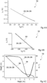
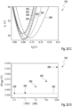
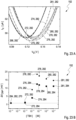
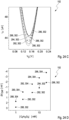
- Figures 4A, 4B and 4C show measurement diagrams 152 recorded with the analyte detector 110 of the type depicted in Figures 3A and 3C .
- Figures 4A and 4B show measurement diagrams 152 recorded in a field-effect transistor-based measurement plotting the drain current I d as a function of the gate voltage V g for three different measurements corresponding to 0 minutes (232), 5 minutes (234) and 10 minutes (236) of incubation in MES (2-(N-morpholino)ethanesulfonic acid) buffer.
- MES 2-(N-morpholino)ethanesulfonic acid
- Figures 4A and 4B each show a stable and reproducible baseline in buffer for the field-effect transistor-based measurement.
- Figure 4C is a measurement diagram 152 of an electrochemical measurement plotting a magnitude of an impedance Z (y-axis on the left-hand side 186) and a phase shift angle ⁇ (y-axis on the right-hand side 184) as a function of frequency f of an alternating voltage for three different measurements corresponding to 0 minutes (232), 5 minutes (234) and 10 minutes (236) of incubation in buffer.
- the measurement diagram 152 shows three impedance measurements and three phase shift angle ⁇ measurements. Again, both for the impedance and for the phase shift measurement, for the most part the three graphs of the three different measurements overlap, being indistinguishable or hardly distinguishable from one another.
- the multipurpose electrode 112 may comprise at least one functional component 153 exposed to its surface 155, as shown in Figures 7B and 9C , wherein the at least one functional component 153 may be configured for interacting with the analyte.
- the functional component 153 may comprise at least one receptor compound being capable of binding the at least one analyte.
- the receptor compound being able of detecting the at least one analyte may be selected from the group consisting of: antibodies and fragments thereof, aptamers, peptides, enzymes, nucleic acids, receptor proteins or binding domains thereof and hydrophilic polymers capable of mediating a salting out effect.
- Figure 5 shows a measurement diagram 152 displaying data recorded with an analyte detector 110 comprising an extended-gate field-effect transistor 144 comprising an extended gate electrode 146 that has a gold layer 150 exposable to the fluid sample 111.
- the multipurpose electrode 112 may comprise the extended gate electrode 146 comprising the gold layer 150.
- Figure 5 shows a field-effect transistor-based measurement plotting the drain current I d versus the gate voltage V g for three different measurement situations, namely using an extended gate electrode 146 with gold layer 150 of bare gold 154, using an extended gate electrode 146 with a gold layer 150 after immobilization of double stranded DNA 156 on the gold layer 150 and using an extended gate electrode 146 with a gold layer 150 after dehybridization of the double stranded DNA 158 on the gold layer 150.
- the field-effect transistor-based measurement can clearly distinguish between the presence of double stranded DNA molecules on the extended gate electrode 146 (graph 156) and single stranded DNA molecules on the extended gate electrode 146 after dehybridization (graph 158).
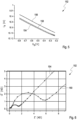
- the analyte detector 110 may also be used for an electrochemical measurement, for example for an impedance measurement that may be able to distinguish between the presence of single stranded DNA (graph 160) and absence of single stranded DNA (graph 154) on the gold layer 150 of the multipurpose electrode 112 as can be seen in the measurement diagram 152 in Figure 6 .
- the measurement diagram 152 in Figure 6 plots the negative imaginary part of the impedance Z'' versus the real part of the impedance Z' for the two different measuring situations just described.
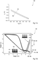
- Figures 7A and 7B illustrate again the ability of the analyte detector 110 to distinguish between the presence of single stranded DNA 160 and the presence of double stranded DNA 161 both in a field-effect transistor-based measurement ( Figure 7A ) and in an electrochemical measurement ( Figure 7B).
- Figure 7A shows a measurement diagram 152 plotting the drain current I d versus the gate voltage V g for two different measuring situations, namely the presence of single stranded DNA 160 as probe DNA on the gold layer 150 of the extended gate electrode 146 of the extended-gate field-effect transistor 144 and the presence of double stranded DNA 161 as a result of hybridization of single stranded probe DNA with single stranded target DNA after the addition of 1 ⁇ M of single stranded target DNA.
- the single stranded probe DNA serves as the functional component 153.
- Figure 7B plots the magnitude of the impedance Z and the phase shift angle ⁇ as a function of the frequency f of the alternating voltage for the same two measuring situations as just described. The two graphs corresponding to the phase shift angle ⁇ in the presence of single stranded DNA 160 and in the presence of double stranded DNA 161 are clearly distinguishable from one another.
- Figures 8A and 8B show measuring diagrams 152 based on field-effect transistor-based measurements using an extended-gate field-effect transistor 144 with an extended gate electrode 146 comprising a gold layer 150 with single stranded probe DNA immobilized on the gold layer 150.
- Figure 8A plots the drain current I d as a function of the potential V ref of the reference electrode 132 in the presence of 1 nM target DNA 163 and in the absence of target DNA 162.
- the field-effect transistor-based measurement is clearly able to detect a potential shift ⁇ V in the presence of target DNA 160 as indicated by the arrow.
- Figure 8B plots a potential shift ⁇ V as a function of target DNA concentration for two different ionic strengths of buffer solution (10 mM and 100 mM). The size of the potential shift ⁇ V increases with increasing target DNA concentration and with increasing Debye length in lower ionic strength buffer.
- Figure 9A and Figure 9B show measurement diagrams 152 based on electrochemical measurements carried out using the electrochemical measurement device 116 of the analyte detector 110 comprising a multipurpose electrode 112 with a gold layer 150 modified with an aminothiophenol monolayer 164 carrying an anti-TSH antibody, where TSH stands for thyroid stimulating hormone.
- Figure 9B plots the reactance X, i.e. the imaginary part of the impedance Z, versus the resistance R, i.e.
- FIG. 9A shows that the analyte detector 110 may be able to detect as little as 1 pM of TSH, demonstrating a potential high sensitivity of the analyte detector 110 and its potential use in medical applications.
- Figure 9C shows a schematic view of the layered modifications of the multipurpose electrode 112 as used in the electrochemical measurements of Figures 9A and 9B , comprising the anti-TSH antibody 166 as the functional component 153.
- the anti-TSH antibodies that are used and/or described in this experiment or other experiments or in this embodiment or in other embodiments, specifically in Figures 11 , 19 and 20 may be anti-TSH F(ab')2-fragments of an anti-TSH antibody that may also be denoted as anti-TSH F(ab')2 fragments.
- Figures 10A and 10B show measurement diagrams 152 plotting the reactance X, i.e. the imaginary part of the impedance Z, versus the resistance R, i.e. the real part of the impedance Z.
- the multipurpose electrode 112 has a gold layer 150 modified with a monolayer 164 and anti-TSH antibodies 166 as shown in Figure 9C .
- the impedance measurement carried out between the multipurpose electrode 112 and the counter electrode 168 can distinguish clearly between five different concentrations of TSH.
- the impedance measurement is carried out between the multipurpose electrode 112 having a gold layer 150 carrying an aminothiophenol monolayer 164 (self-assembled SAM) and the counter electrode 168 in the absence of further modifications of the gold layer 150 of the multipurpose electrode 112, thus in the absence of anti-TSH antibodies, and in the absence of TSH.
- the aminothiophenol monolayer 164 may be a self-assembled monolayer (SAM).
- a drift of the six impedance measurements may be due to the time elapsed during a measurement process.
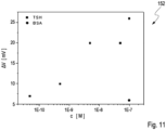
- Figure 11 shows a measurement diagram 152 based on field-effect transistor-based measurements using a field-effect transistor 114 with an extended gate electrode 146 that has a gold layer 150 modified with anti-TSH F(ab')2 antibody fragments 170 as functional components 153.
- the fragments 170 are immobilized on the extended gate electrode 146 via short (0.5 kDa) bifunctional PEG linker molecules (thiol and carboxyl groups to attach PEG to the gold layer 150 and to the anti-TSH F(ab') antibody fragments 170, respectively).
- a long (10 kDa) monofunctional (thiolated) PEG is added to the gold layer 150 as a desalting agent.
- a voltage shift ⁇ V is depicted, given in millivolts (mV), as a function of the concentration c of the compound (analyte TSH or control sample BSA), given in mol/l, BSA standing for bovine serum albumin.
- mV millivolts
- FIG 11 clearly show that the analyte detector 110 is able to distinguish between the presence of TSH and BSA and between different concentrations of TSH when the extended gate electrode 146 is modified with anti-TSH F(ab')2 antibody fragments (170).
- the analyte detector 110 comprises a field-effect transistor 114.
- the multipurpose electrode 112 may be at least partially identical with at least one element selected from the group consisting of the gate electrode 120 of the field-effect transistor 114 and the channel 126 of the field-effect transistor 114.
- Figure 12A shows a field-effect transistor 114 implemented as a liquid-gated FET, comprising a source electrode 122 and a drain electrode 124, a channel 126 and a gate electrode 120.
- the gate electrode 120 in Figure 12A comprises the reference electrode 132 and the conductive electrolyte solution 238.
- the multipurpose electrode 112 in Figure 12A is at least partially identical with the channel 126.
- the channel 126 in Figure 12A comprises a graphene layer 172.
- the semiconducting layer 148 is identical to the graphene layer 172.
- the graphene layer 172 comprises a surface 130 accessible to the analyte.
- a field-effect transistor 114 depicted in Figure 12A further comprises a reference electrode 132.
- Figure 12B shows a partial view of a field-effect transistor 114 of the type schematically depicted in Figure 12A.
- Figure 12C shows a measurement diagram 152 recorded with a field-effect transistor 114 of the type schematically depicted in Figure 12A plotting the current I d as a function of the voltage V ref for different pH values.
- the analyte detector 110 comprises at least one electrochemical measurement device 116 configured for performing at least one electrochemical measurement using the multipurpose electrode 112.
- the electrochemical measurement device 116 is not depicted in this Figure and may be added in electrical connection to the multipurpose electrode 112.
- the electrochemical measurement may comprise at least one measurement selected from the group consisting of: a cyclic voltammetry measurement; an impedance measurement; a potentiostatic measurement; an amperometric measurement; an electrochemical impedance spectroscopy; voltammetry; amperometry; potentiometry; coulometry.
- Figures 13A and 13B show measurement diagrams 152 based on electrochemical measurements, namely the cyclic voltammetry measurement ( Figure 13A ) and an impedance measurement ( Figure 13B ), where the graphene layer 172 described in Figure 12A and 12B served as multipurpose electrode 112 in the electrochemical measurement.
- the measurement diagram 152 shown in Figure 13A plots a current I CV measured between the multipurpose electrode 112 and the counter electrode 168 as a function of a voltage V applied.
- the measurement diagram 152 shown in Figure 13B plots the negative imaginary part of the impedance Z" (the imaginary part also often being referred to as the "reactance" X) versus the real part of the impedance Z' (also often referred to as the "resistance" R).
- Figures 13C and 13D show measurement diagrams 152 based on field-effect transistor-based measurements, carried out using the same multipurpose electrode 112 comprising the graphene layer 172 that served a multipurpose electrode 112 in the electrochemical measurement depicted in the measurement diagrams 152 in Figures 13A and 13B .
- the data depicted in the measurement diagram 152 in Figure 13C were recorded with a field-effect transistor 114 implemented as an ion-sensitive field-effect transistor 114.
- the data depicted in the measurement diagram 152 in Figure 13D were recorded using a field-effect transistor 114 implemented as an extended-gate field-effect transistor 144.
- Both Figure 13C and Figure 13D show the drain current I d plotted as a function of the gate voltage V G .
- the graphene layer 172 may be at least partially covered by metal particles 174, specifically by gold particles 176 as can be seen in Figure 15A .
- Figure 14A to Figure 14D show measurement diagrams 152 corresponding to the measurement diagrams shown in Figures 13A to 13D with the graphene layer 172 of the multipurpose electrode 112 being partially covered by gold particles 174.
- Figures 15B and 15C show the graphene layer 172 with gold particles 176 deposited by physical adsorption overnight ( Figure 15B ) and by 5 minutes of electrodeposition ( Figure 15C ).
- Figures 16A, 16B and 16C show measurement diagrams 152 recorded with the analyte detector 110 using a multipurpose electrode 112 comprising a graphene layer 172 partially covered by gold particles 176.
- gold particles 176 may be deposited on the graphene layer 172 by electrodeposition. The duration of the electrodeposition may be varied.
- Figure 16A shows several field-effect transistor-based measurements carried out using a gate electrode 120 comprising a graphene layer 172 partially covered by gold particles 176, where the duration of deposition of gold particles 176 on the graphene layer 172 varied between 0 and 80 minutes.
- Figure 16B shows several impedance measurements carried out using the multipurpose electrode 112 comprising a graphene layer 172 partially covered by gold particles 176, where the duration of deposition of gold particles 176 on the graphene layer 172 varied between 0 and 30 minutes.
- Figure 16C shows the corresponding measurement carried out after a deposition duration of 80 minutes.
- Figure 17 shows a measurement diagram 152 depicting an amperometric measurement.
- a current I between the multipurpose electrode 112 and the counter electrode 168 is plotted as a function of time t for three different measurements, where each measurement uses a multipurpose electrode 112 comprising a graphene layer 172, where the graphene layer 172 either has no metal particles 174 deposited onto it (0') or the graphene layer 172 has gold particles 176 deposited onto it by electrodeposition for 40 minutes (40') or for 60 minutes (60').
- the three amperometric measurements displayed in Figure 17 were carried out in the presence of 3 different concentrations of an electroactive species [Fe(CN) 6 ] 4- : 2.5, 12.5 and 25 mM.
- the current increases with increasing [Fe(CN) 6 ] 4- concentration.
- the observed current changes are more pronounced for the graphene layer 172 having gold particles 176 deposited onto it, with a deposition time of 60 minutes resulting in a higher sensitivity than a deposition time of 40 minutes.
- Both field-effect transistor-based measurements and electrochemical measurements may be carried out in the presence of polyethylene glycol (PEG), specifically in the presence of pyrene PEG (P-PEG) and/or thiolated PEG (S-PEG) as shown in the measurement diagrams 152 in Figures 18A and 18B.
- Figure 18A shows a measurement diagram 152 of a field-effect transistor-based measurement plotting the drain current I d as a function of the gate voltage V g .
- the measurement was carried out using a field-effect transistor 114 comprising a graphene layer 172 partially covered by the gold particles 176 deposited onto the graphene layer 172 by electrodeposition for 40 minutes.
- Figure 18B shows a measurement diagram 152 of an impedance measurement carried out either in the absence of PEG 178 or in the presence of pyrene PEG 180 or in the presence of thiolated PEG 182.
- the analyte detector 110 may be able to detect TSH and/or distinguish between different concentrations of TSH via the field-effect transistor-based measurement, as shown in Figures 10 A , 19B and 19C and/or via the electrochemical measurement, specifically via the impedance measurement as shown in Figure 20 .
- the multipurpose electrode 112 may comprise a graphene layer 172 as shown in Figure 19A .
- the graphene layer 172 may be prepared by a graphene transfer onto the multipurpose electrode 112.
- the graphene layer 172 may be modified by the addition of PEG, in particular by the addition of thiolated PEG (S-PEG), specifically by the addition of short (0.5 kDa) bifunctional carboxylated thiol PEG (SH-PEG-COOH) 240 , which may at least partially serve as binding sites for the functional component 153, which may comprise anti-TSH antibodies 170, in particular F(ab)'2 TSH-antibody fragments, as shown in Figure 19A .
- the graphene layer 172 may also be modified by co-immobilization of a long (10 kDa) monofunctional methoxy-terminated thiol PEG (SH-PEG-OCH 3 ) 242 which may increase the effective Debye length.
- FIGS 19B and 19C show measurement diagrams 152 that are recorded using the multipurpose electrode 112 of the type depicted in Figure 19A .
- the current I d is plotted as a function of the voltage V ref of the reference electrode 132.
- Figure 19C plots the voltage shift ⁇ V CNP as a function of the concentration c of TSH, which serves as the analyte in this experiment, or the concentration of BSA, which serves as a control sample in this experiment.
- CNP stands for charge neutrality point.
- the shift ⁇ V CNP depicted in Figure 19C may be calculated from the measurement diagram 152 in Figure 19B as the difference between the x-coordinate of the minimum of a graph corresponding to a sample containing TSA (190, 192, 200, 202, 204, 206, 208) and the x-coordinate of graph 188 corresponding to a sample without TSH.
- the x-axis in Figure 19C displays the concentration c on a logarithmic scale.
- Figures 19B and 19C show that the analyte detector 110 may be able to distinguish clearly between at least six different concentrations of TSH using the field-effect transistor 114.
- the multipurpose electrode 112 of the type depicted in Figure 19A may also be used for the impedance measurement depicted in Figure 20.
- Figure 20 shows a measurement diagram 152 plotting the reactance X versus the impedance R.
- Figure 20 shows that the analyte detector 110 may be able to reproducibly detect 1 nM of TSH 194 using the electrochemical measurement device 116, in particular the impedance measurement.
- the analyte detector 110 may also be configured for the analysis of a gaseous analyte.
- the analyte detector 110 may be configured for the analysis of at least one blood gas, specifically of CO 2 .
- Figure 21A shows a partial view of an analyte detector 110, whose multipurpose electrode 112 is at least partially covered by a membrane 214.
- the membrane 214 may comprise or consist of PDMS.
- the membrane 214 may be at least partially permeable by the analyte.
- the analyte detector 110 as shown in the sectional view in Figure 21A may further comprise a space 216 between the membrane 216 and the multipurpose electrode 112.
- the space 216 may be partially filled with an electrolyte 218 as also shown in Figure 21A , specifically with a hydrogel electrolyte, more specifically with a bicarbonate buffer dissolved in an agarose hydrogel.
- the multipurpose electrode 112 shown in Figure 21A may have a surface 130 that may be sensitive to a pH.
- Figure 21B shows a measurement diagram 152 plotting the current I d on a logarithmic scale as a function of the voltage V ref for five different CO 2 partial pressures that are given in the unit of mm Hg.
- the measurement shown in Figure 21B is recorded in an extended-gate field-effect transistor-based measurement with the analyte detector 110 of the type depicted in 21A.
- Figure 21C shows a measurement diagram 152 plotting the voltage shift ⁇ V as a function of the CO 2 partial pressure with the CO 2 partial pressure given on a logarithmic scale on the x-axis.
- the data points displayed in the measurement diagram 152 are derived from the data displayed in Figure 21B.
- Figures 21B and 21C show that the analyte detector 110 may be able to distinguish between deionized water 220 and at least five different CO 2 partial pressures 222, 224, 226 and 228.
- FIGs 22A to 22D show measurement diagrams 152 of an electrochemical measurement in form of a capacitance measurement ( Figures 22A and B ) and of a transistor-based measurement ( Figures 22C and D ) of TSH molecules 199 both measurements using the same multipurpose electrode 112.
- the multipurpose electrode 112 is used to detect the analyte TSH 199 using two different measurement techniques, one transistor-based method and one electrochemical method, that make use of one and the same multipurpose electrode 112.
- the employed multipurpose electrode 112 is of the type illustrated in Figure 19A and described in the corresponding text passage.
- the multipurpose electrode 112 used for TSH molecule 199 detection as shown in the measurement diagrams 152 of Figures 22A to 22D comprises the graphene layer 172 modified by short (approx. 0.5 kDa) bifunctional carboxylated PEG 240, which may at least partially serve as binding sites for the functional component 153, which in this case comprise anti-TSH antibodies 170, in particular F(ab') 2 TSH-antibody fragments.
- the graphene layer 172 is further modified by co-immobilization of a long (10 kDa) monofunctional methoxy-terminated thiol PEG (SH-PEG-OCH 3 ) 242 which may increase the effective Debye length.
- Figure 22A shows the capacitance C in ⁇ F as a function of a frequency f in Hz of an alternating voltage applied for five different situations, in which the fluid sample is either buffer without TSH molecules 199 or the fluid sample is buffer comprising one of the following TSH concentrations: 0.1 nM TSH, 1 nM TSH, 10 nM TSH or 100 nM TSH.
- the different TSH concentrations are marked by reference numbers 244, 246, 248, 250 and 252, respectively.
- Figure 22B shows the capacitance C in ⁇ F as a function of the concentration of TSH molecules 199 in nm for a voltage alternating at 10 -1 Hz, wherein the concentration of TSH molecules 199 is plotted in a logarithmic scale.
- the capacitance C of the buffer without TSH molecules 199 is indicated in Figure 22B by a straight line marked with the corresponding reference number 244.
- the current I d is plotted as a function of the gate voltage Vg of the gate electrode 120 of the FET 114 for seven different situations, in which the fluid sample is either buffer without TSH molecules 199 and without BSA or the fluid sample is buffer comprising 100 nM BSA and no TSH molecules 199 or the fluid sample is buffer comprising one of the following TSH concentrations and no BSA: 100 fM TSH, 1 pM TSH, 50 pM TSH, 100 pM TSH or 1 nM TSH.
- the different concentrations of TSH 199 and BSA are marked by reference numbers 254, 256, 258, 260, 262, 264 and 266, respectively.
- the measurement setup as shown in Figure 2 was used.
- Figure 22D plots the voltage shift ⁇ V CNP as a function of the concentration of TSH 199.
- CNP stands for charge neutrality point.
- the shift ⁇ V CNP may be calculated from the measurement diagram 152 in Figure 22C as the difference between the x-coordinate of the minimum of a graph corresponding to a sample containing TSH (258, 260, 262, 264 and 266) or BSA (256) and the x-coordinate of the graph corresponding to the sample 254 without TSH and BSA.
- the x-axis in Figure 22D displays the concentration of TSH on a logarithmic scale.
- the shift ⁇ V CNP of sample 256 containing buffer comprising 100 nM BSA and no TSH molecules 199 is indicated in Figure 22D by a straight dashed line marked with the corresponding reference number 256.
- Figures 22B and 22D show that by making use of both an electrochemical measurement and a transistor-based measurement a measuring range of the analyte detector 110 may be enhanced significantly as compared to analyte detectors making use of just one measurement method.
- the measurement range of the electrochemical measurement performed as capacitance measurement covers mainly the nanomolar (nM) range while the measurement range of the transistor-based measurement covers mainly the picomolar (pM) range.
- the use of the transistor-based measurement in addition to the electrochemical measurement may enlarge the measurement range of the analyte detector 110 substantially, for example by one or even several orders of magnitude.
- Figure 23A shows a further example of a transistor-based measurement of TSH 199 carried out with a field-effect transistor 114 of the same type as used for acquiring the data displayed in Figures 22C and 22D .
- the current I d is plotted as a function of the gate voltage V g of the gate electrode 120 of the FET 114 for eight different situations, in which the fluid sample is either buffer without TSH molecules 199 or the fluid sample is buffer comprising one of the following TSH concentrations: 10 fM TSH, 1 pM TSH, 10 pM TSH, 50 pM TSH, 100 pM TSH, 1 nM TSH or 10 nM TSH.
- FIG. 23B plots the voltage shift ⁇ V CNP as a function of the concentration of TSH 199 for the data displayed in Figure 23A , which constitutes a first set of measurements.
- the ⁇ V CNP values calculated from the data in Figure 23A are marked with reference sign 282.
- the shift ⁇ V CNP may be calculated from the measurement diagram 152 in Figure 23A as described above for Figures 22C and 22D .
- Figure 23B further plots ⁇ V CNP values originating from a separate FET measurement, which constitutes a second set of measurements. The first set and the second set of measurements were carried out with a separate FET 114.
- ⁇ V CNP values are plotted. These ⁇ V CNP values are marked with reference sign 284.
- TSH concentration of 10 fM which is marked by reference number 270, the measurements of the first set of measurements 282 and the second set of measurements 284 overlap.
- the reference point for the formation of ⁇ V CNP was determined using a real-time measurement in this case and is not shown here.
- Figures 23A and 23B illustrate again that the FET-based measurement of the analyte detector 110 covers a measurement range comprising the picomolar range.
- Figures 24A to 24D show measurement diagrams 152 of an electrochemical measurement in form of a cyclic voltammetry measurement ( Figures 24A and 24B ) and of a transistor-based measurement ( Figures 24C and 24D ) of glucose. Again, both measurements employ the same multipurpose electrode 112.
- the multipurpose electrode 112 is used to detect the analyte glucose using two different measurement techniques, one transistor-based method and one electrochemical method, which make use of one and the same multipurpose electrode 112.
- a multipurpose electrode 112 comprising a graphene layer 172 is employed, wherein the graphene layer 172 is modified such that glucose dehydrogenase (GDH) is immobilized on the graphene layer 172.
- GDH glucose dehydrogenase
- PBA-NHS 1-pyrenebutyric acid N-hydroxysuccinimide ester
- Immobilization of PBA-NHS preferably occurs by applying PBA-NHS, e.g. in a concentration of 1 mM, in a solvent, preferably ethanol, to the graphene layer 172.
- GDH may be added preferably in a concentration of 1 mg/mL.
- a redox mediator such as ferrocenemethanol (FcMeOH) may be added.
- FcMeOH ferrocenemethanol
- the multipurpose electrode 112 may be employed as the gate electrode 120 of the FET 114 and allow glucose detection via the FET-based measurement of the analyte detector 110 as shown in Figures 24C and 24D .
- the multipurpose electrode 112 may further be employed as working electrode e.g.
- Figure 24A plots the current density j in ⁇ A/cm 2 against the applied potential E vs. the reference electrode (Ag/AgCl) for six different situations, in which the fluid sample is either buffer without glucose or the fluid sample is buffer comprising one of the following glucose concentrations: 1 mM, 2 mM, 5 mM, 10 mM or 20 mM.
- the different glucose concentrations are marked by reference numbers 286, 288, 290, 292, 294 and 296, respectively.
- the data displayed in Figure 24A constitute a first set of measurements 298 of the electrochemical glucose detection.
- Figure 24B plots ⁇ I / I blank as a function of the concentration of glucose for the data displayed in Figure 24A , which constitutes the first set of measurements 298 of the electrochemical glucose detection.
- concentration of a molecule may throughout this document be denoted by the molecule in squared brackets.
- Figure 24B further plots ⁇ I / I blank values originating from a separate cyclic voltammetry measurement, which constitutes a second set of measurements 300.
- the first set of measurements 298 and the second set of measurements 300 were carried out with separate electrochemical measurement devices 116.
- For the second set of measurements 300 solely the calculated ⁇ I / I blank values are plotted.
- I is a current value corresponding to a current density j
- I blank denotes the current value produced by the sample 286 containing buffer without glucose
- ⁇ I is the difference between the current value of a sample containing glucose and the current value of the sample 286 containing buffer without glucose when both current values are taken at the peak value ( ⁇ 0.3 V).
- Glucose concentration may further be determined with a transistor-based measurement by using a multipurpose electrode 112 as described above, wherein the multipurpose electrode 112 may serve as gate electrode 120
- the current I d is plotted as a function of the gate voltage V g for the six different situations already described for the cyclic voltammetry measurement shown in Figures 24A and 24B , by using the setup as shown in Figure 2 .
- Figure 24D plots the voltage shift ⁇ V CNP as a function of the concentration of glucose.
- the shift ⁇ V CNP may be calculated from the measurement diagram 152 in Figure 24C as the difference between the x-coordinate of the minimum of a graph corresponding to a sample containing glucose (288, 290, 292, 294 and 296) and the x-coordinate of the graph corresponding to the sample 286 without glucose.
- the x-axis in Figure 24D displays the concentration of glucose on a logarithmic scale.
- Figure 24D plots the voltage shift ⁇ V CNP as a function of the concentration of glucose for the data displayed in Figure 24C , which constitute a first set of transistor-based glucose measurements which is denoted by the reference number 302.
- the ⁇ V CNP values in Figure 24D which are calculated from the data in Figure 24C are also marked with reference sign 302.
- Figure 24D further plots ⁇ V CNP values originating from a separate transistor-based measurement, which constitutes a second set of measurements 304.
- the first set of measurements 302 and the second set of measurements 304 were carried out with separate FETs 114.
- the second set of measurements 304 solely the calculated ⁇ V CNP values are plotted.
Landscapes
- Health & Medical Sciences (AREA)
- Life Sciences & Earth Sciences (AREA)
- Chemical & Material Sciences (AREA)
- Molecular Biology (AREA)
- Physics & Mathematics (AREA)
- Engineering & Computer Science (AREA)
- General Health & Medical Sciences (AREA)
- Microelectronics & Electronic Packaging (AREA)
- Chemical Kinetics & Catalysis (AREA)
- Electrochemistry (AREA)
- Analytical Chemistry (AREA)
- Biochemistry (AREA)
- General Physics & Mathematics (AREA)
- Immunology (AREA)
- Pathology (AREA)
- Spectroscopy & Molecular Physics (AREA)
- Nanotechnology (AREA)
- Investigating Or Analyzing Materials By The Use Of Electric Means (AREA)
- Apparatus Associated With Microorganisms And Enzymes (AREA)
Description
- The invention relates to an analyte detector as defined in
claim 1 and a method for detecting at least one analyte in at least one fluid sample according toclaim 15. The invention further relates to the use of the analyte detector for the qualitative and/or quantitative determination of the at least one analyte in a fluid as defined inclaim 16. - The devices and methods of the present invention, as an example, may be used for diagnostic purposes, e.g. in clinical or laboratory analytics or for home monitoring purposes. The devices and methods of the present invention specifically may be used for detecting one or more analytes in body fluids or other liquids. As an example, DNA detection may be named. Other applications and uses, however, are feasible.
- A wide variety of analyte detectors for detecting at least one analyte in at least one fluid sample have been described. Analyte detectors configured for reliably detecting chemical and/or biological species in a qualitative and/or quantitative manner can be used for various purposes such as, but not limited to, diagnostic purposes, monitoring of environmental contamination, food safety evaluation, quality control or manufacturing processes. Such analyte detectors may for instance rely on transistor-based measurements for identification the at least one analyte. Transistor-based analyte detectors have been adapted to allow the detection of a wide range of analytes including biomolecules such as proteins, antibodies, antigens, DNA, and chemical species such as ionic species and electrolytes.
- A number of studies describe the use of transistor-based analyte detectors in the identification of antigens, antibodies or other proteins: Elnathan et al. (Elnathan et al., Nano Lett. 2012, 12, 5245-5254) describe the detection of proteins in untreated serum and blood samples in the sub-pM concentration range using a nanowire-based field-effect transistor (FET) device combined with size-reduced antibody fragments. The use of size-reduced antibody fragments permits the biorecognition event to occur in closer proximity to the nanowire surface, falling within the charge-sensitive Debye screening length. In a study published by Gao et al. (Gao et al., Nano Lett. 2015, 15, 2143-2148) incorporation of a porous and biomolecule permeable layer on a FET-based nanoelectric sensor is described.
- The polymer layer increases the effective screening length in the region immediately adjacent to the FET-based sensor surface and thereby enables the detection of biomolecules in high ionic strength solutions in real-time. The same study also reports that silicon nanowire field-effect transistors with additional polyethylene glycol (PEG) modification can readily detect prostate specific antigen (PSA) in solutions with phosphate buffer concentrations as high as 150 mM. Kim et al. (Kim et al., Biosens Bioelectron. 2009 Jul15;24(11):3372-8) present a simple and sensitive method for real-time detection of a prostate cancer marker (PSA-ACT complex) through label-free protein biosensors based on a carbon nanotube field-effect transistor (CNT-FET). Tarasov et al. (Tarasov et al., 2D Mater. 2 (2015) 044008) use gold-coated graphene FETs to measure the binding affinity of a specific protein-antibody interaction. In a different study, Tarasov et al. (Tarasov et al., Biosens Bioelectron. 2016 May 15;79:669-78) employ an extended-gate field-effect transistor for direct potentiometric serological diagnosis using the model pathogen Bovine Herpes Virus-1 (BHV-1). To demonstrate the sensor capabilities as a diagnostic tool, BHV-1 viral protein gE is expressed and immobilized on the sensor surface to serve as a capture antigen for BHV-1-specific antibody (ant-gE). The gE-coated immunosensor was shown to be highly sensitive and selective to anti-gE and significantly faster than Enzyme-Linked ImmunoSorbent Assay (ELISA) that is typically performed by centralized laboratories.
- Other studies explore the potential of transistor-based analyte detectors for the identification of nucleic acids, such as DNA or RNA, or possible components thereof, such as aden-osinmonophosphate (AMP). In
US20100053624 a biosensor is disclosed that can convert biological interactions into electrical and optical signals to sense a material to be analyzed. The biosensor includes a substrate, a source electrode and a drain electrode formed on one surface of the substrate, a carbon nanotube connecting the source and the drain electrodes, a metal gate covering the carbon nanotube, a recognition component immobilized on the metal gate, and a passivation layer covering the source and drain electrodes. In one embodiment, the recognition component may be a single-stranded oligonucleotide such as DNA or RNA. In the case of DNA, the biosensor has a recognition DNA immobilized on the surface of the metal gate. Electrical and/or optical signals are generated as a result of hybridization between the recognition DNA and a target DNA. Zayats et al. (Zayats et al., J Am Chem Soc. 2006 Oct 25;128(42):13666-7) present research applying aptamers for the label-free reagent-less analysis of small molecules. They demonstrate that the small substrate-induced separation of a duplex nucleic acid that includes the aptamer strand, on an ion-sensitive field-effect transistor (ISFET) or on an electrode, forms a substrate-aptamer complex that can be electrically characterized. In particular, an amine-functionalized nucleic acid that acts as aptamer was immobilized on the gate surface and further hybridized with a short nucleic acid. The addition of adenosine displaces the short nucleic acid and assembles the aptamer into the hairpin configuration that binds adenosine mono-phosphate (AMP). - Understanding and controlling the behavior of the analyte detector is crucial for its targeted use. Transistor-based analyte detectors can also respond to chemicals species such as ionic species and electrolytes. Tarasov et al. (Tarasov et al. ACS Nano. 2012 Oct 23;6(10):9291-8) use silicon nanowires coated with highly pH-sensitive hafnium oxide (HfO2) and aluminum oxide (Al2O3) in silicon nanowire field-effect transistor to determine their response to changes in the supporting electrolyte concentration. Wipf et al. (Wipf et al., ACS Nano 2013 Jul 23;7(7):5978-83) modify individual nanowires with thin gold films as a novel approach to surface functionalization for the specific detection of electrolyte ions by ion-sensitive field-effect transistors in a differential setup. They find that a functional self-assembled monolayer does not affect the unspecific response of gold to pH and background ionic species, which represents a clear advantage of gold compared to oxide surfaces.
- Thus, transistor-based analyte detectors have been adapted in numerous ways to detect a multitude of analytes. The advances established in the field of transistor-based analyte detectors are in part due to advances in surface functionalization techniques, in particular those applicable to nano-devices. Shim et al. (Shim et al., Nano Letters 2002 Vol.2, No.4, 285-8) study the adsorption behavior of proteins on the side of single-walled carbon nanotubes. They report that the functionalization of single-walled carbon nanotubes by co-adsorption of a surfactant and polyethylene glycol is found to be effective in resisting non-specific adsorption of streptavidin. In
US7491496B2 a method is disclosed for immobilizing nucleic acid and a method for manufacturing a biosensor using the same method. The method provided enables high-density absorption when immobilizing nucleic acid probes onto a solid support by suppressing electrostatic repulsion among the nucleic acids. A nucleic acid immobilization method to immobilize a nucleic acid onto a solid support, includes: preparing a solution containing a probe molecule which includes a nucleic acid, a spacer molecule, and at least one kind of a divalent cation; and contacting the solution with the solid support for incubation. Yoshimoto et al. (Yoshimoto et al., J Am Chem Soc. 2010 Jun 16; 132(23):7982-9) examine the adsorption behavior of antibody fragments directly immobilized on a gold surface through S-Au linkage. They report that the conformational and/or orientation change of antibody fragments was suppressed by a coimmobilized mixed polyethylene glycol layer. Yoshimoto et al. expect their findings to be useful for the improvement of the antibody fragment method and, thus, for the construction of high-performance immunosensor surfaces. - However, analyte detectors able to detect at least one analyte in at least one fluid sample may also be based on electrochemical measurements. For details of electrochemical test elements and potential test chemicals useful in such test elements, which may also be used within the present invention, reference may be made to J. Hoenes et al.: The Technology Behind Glucose Meters: Test Strips, Diabetes Technology & Therapeutics, Vol. 10, . Further, impedance biosensors are a class of electrical biosensors able to detect unlabeled DNA and protein targets by monitoring changes in surface impedance when a target molecule binds to an immobilized probe. The challenges caused by the affinity capture step and other challenges unique to impedance readout are discussed in Daniels and Pourmand, Electroanalysis, 2007 May 16, 19(12): 1239-1257. Furthermore, in their fundamental study from 1958, Severinghaus and Bradley (Severinghaus and Bradley, J Appl Physiol. 1958 Nov:13(3):515-20) describe an apparatus to permit rapid and accurate analysis of oxygen and carbon dioxide tensions in gas, blood or any liquid mixture using an oxygen electrode and a carbon dioxide electrode. Wu et al. (Wu et al., Sensors and Actuators B 110 (2005) 342-9) report on a miniature Clark-type oxygen sensor that has been integrated with a microstructure using a novel fabrication technique. Moreover, analyte detectors may also combine functional elements as reported by Zhu et al. (Zhu et al., Nano Lett. 2014 Oct 8;14(10):5641-9), who present a graphene enabled, integrated optoelectromechanical device and demonstrate its utility for biomolecular sensing. They demonstrate a novel nanoscale sensing device with optical, electronic and mechanical functional elements integrated on the same chip. By having each element target a different concentration regime, the sensitivity-dynamic range trade-off of traditional single-mode sensors can be significantly mitigated.
-
WO 2016/173542 A1 discloses a system for detecting a target and a method for detecting a target. The system includes a field effect transistor, having a gate, a source, and a drain; a potentiostat, having a working electrode, a counter electrode, and a reference electrode; wherein the working electrode is coupled with a detection region, and the counter electrode is coupled with the gate; wherein the detection region, the gate, and the reference electrode are arranged in an ion fluid; wherein the potentiostat is configured to generate redox in the ion fluid by an electrochemical method to detect the target. - Formisano et al.: "Inexpensive and fast pathogenic bacteria screening using field-effect transistors". BIOSENSORS AND BIOELECTRONICS, ELSEVIER BV, NL, vol. 85, 21 April 2016 (2016-04-21), pages 103-109, ISSN: 0956-5663, DOI: 10.1016/J.BIOS.2016.04.063, describes a label-free sensor for fast bacterial detection based on metal-oxide-semiconductor field-effect transistors (MOSFETs). The electrical charge of bacteria binding to the glycosylated gates of a MOSFET enables quantification in a straightforward manner and at a higher sensitivity than is achieved with electrochemical impedance spectroscopy (EIS) and matrix-assisted laser desorption ionization time-of-flight mass spectroscopy (MALDI-ToF) on the same modified surfaces.
- Vieira et al.: "Label-free electrical recognition of a dengue virus protein using the SEGFET simplified measurement system". Analytical Methods, , describes the use of a separative extended gate field-effect transistor (SEGFET) as an immunosensor for the label-free recognition of dengue virus nonstruc-tural protein 1 (NS1). NS1 is detected in a concentration range of 0.25 to 5.0 µg mL-1, indicating that the system is promising for the early and simple diagnosis of dengue.
-
US 2016/131613 A1 discloses a floating gate based sensor apparatus including at least two separate electrical bias components with respect to a floating gate based sensor surface within the floating gate based sensor apparatus. By including the at least two electrical bias components, the floating gate based sensor apparatus provides enhanced capabilities for biomaterial and non-biomaterial detection and manipulation while using the floating gate based sensor apparatus. - Lin et al.: "Non-Faradaic electrical impedimetric investigation of the interfacial effects of neuronal cell growth and differentiation on silicon nanowire transistors". ACS APPLIED MATERIALS AND INTERFACES, vol. 7, no.18, 13 May 2015 (2015-05-13), pages 9866-9878, US ISSN: 1944-8244, DOI: 10.1021/acsami.5b01878, describes the application of silicon nanowire field-effect transistors (SiNWFET) devices for noninvasive, real-time monitoring of interfacial effects during cell growth and differentiation using cultured rat adrenal pheochromocytoma (PC12) cells. Monitoring of cell adhesion during growth and morphological changes during neuronal differentiation was performed by measuring the non-Faradaic electrical impedance of the cell-SiNW FET system using a precision LCR meter.
- Zhan et al.: "Graphene field-effect transistor and its application for electric sensing". SMALL, 7 July 2014 (2014-07-07), ISSN: 1613-6810, DOI: 10.1002/smll.201400463, describes the fabrication and characterization of graphene based field-effect transistors (GFETs) and introduces the new developments in physical, chemical, and biological electronic detection using GFETs. Further, several perspectives and current challenges of GFETs development are presented, and some proposals are suggested for further development and exploration.
-
US2012/019315 A1 discloses a bio material receiving device including a thin film transistor (TFT) including a drain electrode, and a nano well accommodating a bio material. The drain electrode includes the nano well. The TFT may be a bottom gate TFT or a top gate TFT. A nano well array may include a plurality of bio material receiving devices. In a method of operating the bio material receiving device, each of the bio material receiving devices may be individually selected in the nano well array. When the bio material is accommodated in the selected bio material receiving device, a voltage is applied so that another bio material is not accommodated. - Arquint et al.: "Integrated blood-gas sensor for pO2, pCO2 and pH" SENSORS AND ACTUATORS B: CHEMICAL: INTERNATIONAL JOURNAL DEVOTED TO RESEARCH AND DEVELOPMENT OF PHYSICAL AND CHEMICAL TRANSDUCERS, ELSEVIER BV, NL, vol. 13, no. 1-3, 1 May 1993 (1993-05-01), pages 340-344, ISSN: 0925-4005, DOI: 10.1016/0925-4005(93)85396-R [retrieved on 1993-05-01], describes the fabrication and characterization of a combined pO2, pCO2 and pH chemical sensor, designed for blood gas monitoring. Classical electrochemical principles are used in a miniaturized planar-type structure. Both amperometric (pO2) and potentiometric devices (pCO2, pH) are integrated on a 10 mm x 10 mm chip. The transducer part of the chip is realized using standard silicon technology. Polyacrylamide and polysiloxane layers, which are used as hydrogel and gas-permeable membrane, respectively, are deposited and patterned by photopolymerization. Thus, the whole sensor is fabricated on wafer level using IC-compatible processes. The characterization has been performed in aqueous solutions and in blood used for transfusion. For this purpose, the chip is mounted into a flow-through cell.
- Gutiérrez-Sanz et al.: "Direct, label-free, and rapid transistor-based immunodetection in whole serum" ACS SENSORS 2017 Sep 22;2(9), pages 1278-1286, DOI: 10.1021/acssensors.7b00187, Epub 2017 , describes how tailoring the sensing surface of a transistor-based biosensor with short specific biological receptors and a polymer polyethylene glycol (PEG) can strongly enhance the sensor response. In addition, the sensor performance can be dramatically improved if the measurements are performed at elevated temperatures (37 °C instead of 21 °C). With this novel approach, highly sensitive and selective detection of a representative immunosensing parameter-human thyroid-stimulating hormone-is shown over a wide measuring range with subpicomolar detection limits in whole serum. This allows direct immunodetection in whole serum using transistor-based biosensors, without the need for sample pretreatment, labeling, or washing steps. The presented sensor is low-cost, can be easily integrated into portable diagnostics devices, and offers a competitive performance compared to state-of-the-art central laboratory analyzers.
- Filipiak et al.: "Highly sensitive, selective and label-free protein detection in physiological solutions using carbon nanotube transistors with nanobody receptors" Sensors and Actuators B: Chemical, Volume 255, , describes combining highly stable FETs based on single-walled semiconducting carbon nanotube (SWCNTs) networks with a novel surface functionalization comprising: 1) short nanobody (VHH) receptors, and 2) a polyethylene glycol (PEG) layer. These measures overcome the two major challenges that have limited the use of nanomaterial-based field-effect transistors (FETs) in physiological samples: screening of the analyte charge by electrolyte ions (Debye screening) and non-specific adsorption. Nanobodies are stable, easy-to-produce biological receptors that are very small (~2-4 nm), thus enabling analyte binding closer to the sensor surface. Despite their unique properties, nanobodies have not been used yet as receptors in FET based biosensors. The addition of PEG strongly enhances the signal in high ionic strength environment. Using green fluorescent protein (GFP) as a model antigen, high selectivity and sub-picomolar detection limit with a dynamic range exceeding 5 orders of magnitude is demonstrated in physiological solutions. In addition, long-term stability measurements reveal a low drift of SWCNTs of 0.05 mV/h. The presented immunoassay is fast, label-free, does not require any sample pretreatment or washing steps.
- In the field of analytics, generally, one major technical challenge typically resides in the selection of appropriate methods and devices for the specific analyte to be detected. Even more, in some cases, several types of analytes in one and the same sample may have to be detected. As discussed above, a wide variety of detectors having differing sensitivities and measurement principles is available. Transistor-based detectors, as an example, are highly sensitive to the analyte charge. Analyte detectors based on electrochemical measurements are usually sensitive to the current, impedance or potential changes resulting from electrochemical reactions involving the analyte. Thus, typically, for each analyte to be detected, a specific detector has to be selected, having properties suited for the analyte. The measurement setup, consequently, typically is highly specific for the analyte to be tested for, and the setup, in total, typically lacks versatility. Further, each measurement principle typically has its own drawbacks, technical limitations and inaccuracies. Consequently, the choice of a measurement principle also implies the choice of the technical drawbacks involved with this measurement principle. A combination of measurement principles, however, typically leads to a complex setup and evaluation. There is, consequently, a general need for electronic sensors in physiological liquids which generally provide a high versatility and selectivity and which provide a more universal sensor layout as compared to the methods, measurement principles and devices known in the art.
- It is therefore an objective of the present invention to provide an analyte detector and a method for detecting at least one analyte in at least one fluid sample which at least partially avoid the drawbacks and disadvantages of known measurement principles. Specifically, it is desirable to provide an analyte detector and a method which allow for a high versatility, selectivity and sensitivity and, still, which provide a more universal sensor layout as compared to known means and methods.
- This problem is solved by an analyte detector for detecting at least one analyte in at least one fluid sample and a method for detecting at least one analyte in at least one fluid sample with the features of the independent claims. Preferred embodiments, which might be realized in an isolated fashion or in any arbitrary combination, are listed in the dependent claims.
- As used in the following, the terms "have", "comprise" or "include" or any arbitrary grammatical variations thereof are used in a non-exclusive way. Thus, these terms may both refer to a situation in which, besides the feature introduced by these terms, no further features are present in the entity described in this context and to a situation in which one or more further features are present. As an example, the expressions "A has B", "A comprises B" and "A includes B" may both refer to a situation in which, besides B, no other element is present in A (i.e. a situation in which A solely and exclusively consists of B) and to a situation in which, besides B, one or more further elements are present in entity A, such as element C, elements C and D or even further elements.
- Further, it shall be noted that the terms "at least one", "one or more" or similar expressions indicating that a feature or element may be present once or more than once typically will be used only once when introducing the respective feature or element. In the following, in most cases, when referring to the respective feature or element, the expressions "at least one" or "one or more" will not be repeated, non-withstanding the fact that the respective feature or element may be present once or more than once.
- Further, as used in the following, the terms "preferably", "more preferably", "particularly", "more particularly", "specifically", "more specifically" or similar terms are used in conjunction with optional features, without restricting alternative possibilities. Thus, features introduced by these terms are optional features and are not intended to restrict the scope of the claims in any way. The invention may, as the skilled person will recognize, be performed by using alternative features. Similarly, features introduced by "in an embodiment of the invention" or similar expressions are intended to be optional features, without any restriction regarding alternative embodiments of the invention, without any restrictions regarding the scope of the invention and without any restriction regarding the possibility of combining the features introduced in such way with other optional or non-optional features of the invention.
- In a first aspect of the present invention, an analyte detector for detecting at least one analyte in at least one fluid sample is disclosed. The analyte detector is defined in
claim 1. - As used herein, the term "analyte detector" may generally refer to an arbitrary device configured for an analytical examination of the sample. The analyte detector may be configured for conducting at least one analysis, such as a medical analysis, of the sample. As generally used within the present invention, the terms "analysis", "analytical examination" and "determination of one or more analytes" are used synonymously and are understood to describe a qualitative and/or a quantitative detection of the at least one analyte. In particular, said terms may be understood as a determination of the concentration or amount of the respective analyte, where the sole determination of the absence or presence of the analyte may also be regarded as an analytical examination. Thus, specifically, the analyte detector may be configured for qualitatively and/or quantitatively detecting one or more analytes, specifically in one or more samples. The detection of the at least one analyte may take place at a high degree of sensitivity.
- As further used herein, the term "analyte" generally may refer to an arbitrary chemical or biological substance or species, such as an ion, an atom, a molecule or a chemical compound. The analyte specifically may be an analyte which may be present in a bodily fluid or a body tissue. The term analyte specifically may encompass atoms, ions, molecules and macromolecules, in particular biological macromolecules such as nucleic acids, peptides and proteins, lipids, sugars, such as glucose, and metabolites. Further examples of potential analytes to be detected will be given in further detail below.
- As used herein, the term "fluid sample" generally may refer to a liquid or gas. The fluid sample may have a defined or definable volume. Further, the fluid sample may be comprised in a defined or definable space or may also be present in an open space such as in an open surrounding. The fluid sample may be present in a static state or may flow continuously or discontinuously. The fluid sample may, as an example, be a pure liquid or a homogeneous or heterogeneous mixture, such as a dispersion, an emulsion or a suspension. Similarly, for gases, mixtures of gases or even mixtures of gases with liquids or solids may be used.
- In particular, the fluid sample can contain atoms, ions, molecules and macromolecules, in particular biological macromolecules such as nucleic acids, peptides and proteins, lipids and metabolites, and also biological cells and cell fragments. Typical fluid samples to be examined are bodily fluids such as blood, plasma, serum, urine, cerebrospinal fluid, lachrymal fluid, cell suspensions, cell supernatants, cell extracts, tissue lysates or such likes. Fluid samples can, however, also be calibration solutions, reference solutions, reagent solutions or solutions containing standardized analyte concentrations, so-called standards.
- As used herein, the term "electrode" may generally refer to a functional element configured to perform a current measurement and/or a voltage measurement and/or configured to apply a current and/or an electrical potential and/or a voltage to an element in electrical contact with the electrode. In particular, the electrode may comprise a conducting and/or a semiconducting material. As an example, the electrode may comprise at least one metallic material and/or at least one organic or inorganic semiconducting material, having at least one conducting or semiconducting surface. The surface itself may form the electrode or a part of the electrode. As an example, the electrode may comprise at least one material, specifically at least one surface material, having an electrical conductivity of at least 1000 S/m, e.g. at least 1000000 S/m, either isotropically or anisotropically in at least one direction.
- As used herein the term "in electrical contact" may generally refer to the arrangement or configuration of at least two components, wherein at least one of the components is able to electrically influence the at least one other component and/or to at least partially control an electrical quality of the other component such as, but not limited to, its conductivity and electrical current flow, for instance via field effects. In particular, an electrode may be in electrical contact with an element without being in direct physical contact with said element. Thus, an electrode may control the electrical current flow within an element by application of a voltage despite being insulated from said element. Insulation may, for instance, be constituted by an oxide layer as is typically the case for a gate electrode of a metal oxide semiconductor field-effect transistor (MOSFET) a subgroup of insulated-gate field-effect transistors (IGFET), which is described in more detail below. Thus, generally, for being in electrical contact with each other, the at least two components may be located in close proximity, without being in direct physical contact with one another, such that, however, the components may influence one another electrically. Additionally or alternatively, however, the at least two components may also be physically connected via at least one connecting element having at least semiconducting properties or electrically conductive properties, such as by at least one electrical conductor. Again, the at least two components are separate components or are fully or partially integrated into one another. As an example, the at least one multipurpose electrode may either be connected to the field-effect transistor via at least one connecting element, such as via at least one electrically conductive lead, or may even fully or partially be integrated into the field-effect transistor. Various possibilities are given.
- As used herein, the term "multipurpose electrode" may generally refer to an arbitrary electrode configured to be able to form part of at least two different measurement devices. Thus, the multipurpose electrode may take part in analytical examinations based on at least two different methods, wherein each of the methods requires the use of at least one measurement device. The multipurpose electrode may, for instance, be configured to form part of at least both the field-effect transistor and the electrochemical measurement device. Thus, the multipurpose electrode may take part in analytical examinations based on at least one of the methods comprising the use of the field-effect transistor and the at least one other method comprising the use of the electrochemical measurement device.
- As further used herein, the term "exposable" generally refers to the property of an element of providing at least one surface which may be brought into contact with the at least one substance to which the element is to be exposed. Thus, as an example, the at least one multipurpose electrode may provide at least one electrode surface accessible to the fluid sample. Specifically, as will be explained by exemplary embodiments below, the analyte detector may comprise at least one fluid channel, such as a fluid channel having an inlet port and an outlet port, through which the fluid sample may flow, wherein the at least one multipurpose electrode comprises at least one electrode surface accessible from the fluid channel, such that liquid flowing through or present in the fluid channel contacts the at least one electrode surface. Other options, however, are feasible.
- As further used herein, the term "field-effect transistor" may generally refer to a functional element comprising at least one source electrode, at least one drain electrode and at least one gate electrode. The field-effect transistor further comprises at least one channel. As used herein, the term "channel" of the field-effect transistor may generally refer to a component able to conduct a current between the source electrode and the drain electrode. The channel may have at least one semiconducting material and/or at least one doped semiconducting material. The semiconducting material may be or may comprise at least one of an inorganic semiconducting material and an organic semiconducting material. Typically, a semiconducting material exhibits an electrical conductivity σ of 10-8 S/cm < σ < 104 S/cm.
- In the field of organic semiconductors, however, due to the impact of the low charge carrier mobilities, due to the molecular orbitals and/or due to the low charge carrier densities, however, this description is often not fully applicable. Thus, organic conductive materials are often denoted as organic semiconductors, even though their conductivity may be higher than 104 S/cm, such as graphene.
- In particular, the semiconducting material may comprise one, two or more regions, preferably two to ten regions, more preferably three regions, wherein each region may be n-type doped or p-type doped. Specifically the semiconducting material may comprise an inorganic and/or organic semiconducting material. The channel may be able to conduct a current between the source electrode and the drain electrode only under specific external conditions. The conditions may include a temperature of the channel and/or the voltage or electrical potential applied to the channel either directly or via the gate electrode or via an external electrode. In particular, the channel may be constituted by at least one semiconducting material, such as by at least one semiconducting layer. As an example, inorganic and/or organic semiconducting materials may be used. In the following, as a specific example, graphene is used as a semiconducting material, such as by using one or more graphene layers. The gate electrode may be in direct physical contact with the channel. In this configuration the field-effect transistor may generally be referred to as "non-insulated-gate field-effect transistor" (NIGFET). In particular, the gate electrode may be at least partially identical with the channel. Alternatively, the gate electrode may be in indirect physical contact with the channel, e.g. by using one or more electrically insulating materials interposed in between the gate electrode and the channel. In this configuration the transistor may generally be referred to as "insulated-gate field-effect transistor" (IGFET).
- The insulated-gate field-effect transistor may be implemented as a "metal-insulator-semiconductor field-effect transistor" (MISFET). In this case, the gate electrode which may comprise at least one metal may be insulated from the channel which may comprise at least one semiconducting material. Specifically, the insulation of the gate electrode from the channel may be constituted by an oxide. In this configuration the field-effect transistor may generally be referred to as "metal-oxide-semiconductor field-effect transistor" (MOSFET). However, other materials for insulation of the gate electrode are feasible. The channel of the field-effect transistor may be in physical contact with an electrolyte solution, which may constitute or form part of the gate electrode. In this configuration an ionic double layer may form, that may serve as insulation of the gate electrode from the channel. In this configuration the field-effect transistor may be referred to as a "solution-gated or liquid-gated FET". The electrolyte solution may comprise substances that may influence the potential applied to the channel upon close proximity or adsorption to the channel and/or the insulation of the channel, thus allowing the detection of chemical species. In this configuration the field-effect transistor may be referred to as a "chemical field-effect transistor" or ChemFET. In particular a ChemFET may be configured for the detection of ionic species forming an "ion-sensitive field-effect transistor" (ISFET) that may be sensitive to H+ and/or other ionic species. A layer sensitive to ionic species, such as Al2O3, Si3N4 or Ta2O5, may be in contact with the channel or may form part of the gate electrode of the ISFET and/or may form part of the channel and the gate electrode. In another configuration, the ChemFET may comprise a layer of immobilized enzymes as part of the gate electrode and/or the channel of the field-effect transistor. In this configuration the field-effect transistor may be referred to as an "enzyme field-effect transistor" (ENFET). Binding of the enzyme to the analyte may affect the potential applied to the channel and allow detection of the analyte. Thus, the ENFET is an example of a field-effect transistor-based biosensor (BioFET). As a BioFET the field-effect transistor may comprise a layer of immobilized biomolecules as biorecognition elements able to bind one or more species of molecules, specifically biomolecules, where the binding reaction may either directly or indirectly affect the potential applied to the channel.
- The field-effect transistor may further be implemented as an "extended-gate field-effect transistor". As used herein, the term "extended-gate field-effect transistor" may generally refer to a field-effect transistor comprising a gate electrode configured to allow a spatial separation of the channel of the field-effect transistor from a process or reaction that sets or affects the potential of the gate electrode. Such an electrode may generally be referred to as an "extended gate electrode". Thus, the extended gate electrode of an extended-gate field-effect transistor may allow to physically separate the process of applying a potential to the channel and the process of applying a potential to the gate electrode.
- The at least one field-effect transistor may comprise at least one substrate. The substrate may have purely mechanical properties and function, such as for carrying the above-mentioned components of the field-effect transistor. Alternatively, however, the substrate may also be fully or partially identical with one or more of the above-mentioned components. Thus, as an example, the at least one channel may fully or partially be embodied within the substrate.
- The at least one field-effect transistor may further have at least one sensing surface. The at least one sensing surface, as an example, may be a surface of the field-effect transistor which may be exposed to the fluid sample. The sensing surface, as an example, may be a surface of the multipurpose electrode, e.g. the above-mentioned electrode surface. The sensing surface, however, may also be or comprise another surface, such as a surface of the channel of the field-effect transistor. Various embodiments are feasible and will be described in an exemplary fashion in further detail below.
- As used herein, the term "electrochemical measurement" may generally refer to the measurement of at least one measureable characteristic of a redox reaction. The electrochemical measurement and/or the measurable characteristic of the redox reaction, as an example, may imply an electrical current, a voltage, an electrical potential, a mass, for instance a mass deposited on an electrode, an impedance, particularly the real part and/or the imaginary part of the impedance, a capacitance, a resistance or a phase shift. Specifically, the electrochemical measurement may be performed in the presence of an electroactive species. As used herein, the term "electroactive species" may generally refer to a compound that facilitates or enhances or catalyzes the redox reaction, for instance by facilitating an electron transfer. The electroactive species may be dissolved in the fluid sample and/or may be immobilized on a surface of the analyte detector, wherein the surface may be exposable to the fluid sample. In particular, the surface may be the above-mentioned sensing surface and/or the above-mentioned surface of the multipurpose electrode. Preferred examples of electroactive species are redox mediators, specifically redox couples, such as but not limited to: potassium ferricyanid/ potassium ferrocyanide; hexaammineruthenium (II) chloride/ hexaammineruthenium (III) chloride; ferrocene methanol. Further preferred examples of electroactive species are reducing agents such as but not limited to ascorbic acid, glutathione, lipoic acid, uric acid, oxalic acid, tannins and phytic acid. The electroactive species may facilitate or enhance the measurement of the at least one measurable characteristic of the redox reaction. As used herein, the term electrochemical measurement device may generally refer to an arbitrary device configured to perform at least one electrochemical measurement.
- The term "electrochemical measurement device" may generally refer to an arbitrary device configured for performing at least one electrochemical measurement. For this purpose, as will be outlined in further detail and in an exemplary fashion below, the at least one electrochemical measurement device may comprise one or more electrical devices configured for performing the at least one electrochemical measurement. As an example, the electrochemical measurement device may comprise at least one electrical source, such as at least one electrical source selected from the group consisting of: a constant voltage source, a variable voltage source, a constant electrical current source, a variable electrical current source, a frequency generator for generating periodic electrical signals. Further, the electrochemical measurement device may comprise at least one electrical measurement device configured for measuring at least one electrical signal or electrical measurement variable, such as at least one electrical measurement device selected from the group consisting of: a voltage measurement device, a current measurement device, a potentiostat. Other measurement devices are feasible. The field-effect transistor specifically may not be part of the electrochemical measurement device. Thus, in other words, the analyte detector may comprise the field-effect transistor and the electrochemical measurement device as separate devices, consisting of separate components, except for the multipurpose electrode, which may be part of both the field-effect transistor and of the electrochemical measurement device. Thus, generally, the field-effect transistor and the electrochemical measurement device may form separate components of the analyte detector, except for the multipurpose electrode, which may form part of both the field-effect transistor and the electrochemical measurement device. Specifically, the transistor measurement by using the field-effect transistor and the electrochemical measurement by using the electrochemical measurement device may be distinct and separate measurements. The electrochemical measurement may be made without making use of the field-effect transistor.
- The electrochemical measurement and/or the field-effect transistor-based measurement may take place in the presence of at least two different species of biorecognition molecules, for instance at least two different species of receptor molecules, namely at least one first receptor molecule and at least one secondary receptor molecule. The first receptor molecule and the secondary receptor molecule may be able to bind the analyte directly or indirectly. The first receptor molecule and the secondary receptor molecule may bind the analyte simultaneously. The secondary receptor molecule may enhance the electrochemical measurement and/or the field-effect transistor-based measurement, for instance by enhancing a signal and/or a selectivity of the electrochemical measurement and/or of the field-effect transistor-based measurement. The secondary receptor may enhance the signal and/or the selectivity on its own. Additionally or alternatively the secondary receptor may be labelled with at least one additional molecule, such as but not limited to an enzyme. The secondary receptor may affect or enhance the detection of the analyte by the analyte detector through an interaction with the analyte, e.g. through binding the analyte. The direct or indirect interaction of the secondary receptor with the analyte may affect or enhance the electrochemical measurement and/or the field-effect transistor-based measurement for instance by affecting or enhancing or producing a change in a concentration of a chemical species, such as but not limited to protons and/or electrons. The change in a concentration of a chemical species may correspond to a concentration of the analyte in the fluid sample. Thus, the secondary receptor may contribute to a signal enhancement of the analyte detector.
- As outlined above, the electrochemical measurement device is configured for performing the at least one electrochemical measurement by using the at least one multipurpose electrode. Thus, the multipurpose electrode takes part in the electrochemical measurement. As an example, the at least one multipurpose electrode may be in electrical contact with the electrochemical measurement device, such as with the at least one electrical source and/or the at least one electrical measurement device discussed above. The at least one multipurpose electrode may be part of the at least one electrochemical measurement device and/or may be connected to the electrochemical measurement device, such as via at least one electrical connecting element, e.g. via at least one lead.
- The multipurpose electrode may be in electrical contact with a gate electrode of the field-effect transistor. In particular, the gate electrode may be in direct or indirect physical contact with at least one channel of the field-effect transistor, specifically with at least one semiconducting layer. There may, for example, be a dielectric layer between the gate electrode and the channel, for instance to avoid leak current. In the case of a liquid-gated field-effect transistor, an ionic double layer may constitute the dielectric layer. In the embodiments just described, the gate electrode is typically in indirect physical contact with the channel of the field-effect transistor, specifically with the at least one semiconducting layer.
- The multipurpose electrode may be at least partially identical with at least one element selected from the group of the gate electrode of the field-effect transistor and the channel of the field-effect transistor. The field-effect transistor may comprise at least one channel. Specifically, the at least one channel may be fully or partially made of at least one semiconducting material. A complete field-effect transistor typically comprises a semiconducting channel, metal source, drain and gate electrodes. Specifically, the gate electrode may be replaced by a reference electrode in solution or by a pseudoreference electrode, such as a metal electrode in solution. The semiconducting layer may comprise at least one material selected from the group consisting of: inorganic elemental semiconductors, inorganic compound semiconductors, and organic semiconductors. Specifically, the semiconducting layer may comprise at least one material selected from the group consisting of: graphene, a layered semiconductor, carbon nanotubes, and semiconducting nanowires. Further, the semiconducting layer may comprise at least one surface accessible to the analyte. In particular, the at least one surface accessible to the analyte may be functionalized by metal particles, specifically be metal particles comprising one or more metals selected from the group consisting of: gold and platinum. However, the use of other metals or alloys is also feasible.
- The analyte detector may comprise at least one graphene layer interconnecting at least two electrically conductive electrodes, wherein the graphene layer may be accessible to the analyte, wherein the multipurpose electrode may comprise at least one element of the group consisting of: at least one of the at least two electrically conductive electrodes, the graphene layer. As an example, the semiconducting layer comprising, for instance, graphene may be the multipurpose electrode or may be part of the multipurpose electrode. In particular the graphene layer may be the multipurpose electrode or may be part of the multipurpose electrode. In such an embodiment at least one other electrode, specifically the source and/or the drain electrode, may serve to make contact to the semiconducting layer comprising, for instance to the graphene layer. The graphene layer may be at least partially covered by metal particles, specifically by gold particles.
- The at least one multipurpose electrode may be in electrical contact with one or both of a source electrode or a drain electrode of the field-effect transistor. The multipurpose electrode may, for example, comprise the channel of the field-effect transistor. In this embodiment the source electrode and the drain electrode may serve to make contact to the multipurpose electrode. Alternatively, the multipurpose electrode may be fully of partially identical to one or more of: the source electrode; the drain electrode; the gate electrode.
- The analyte detector comprises at least one further electrode exposable to the fluid sample. The at least one further electrode may comprise at least one electrode selected from the group consisting of a counter electrode and a reference electrode, wherein the electrochemical measurement device is configured for performing the at least one electrochemical measurement using the multipurpose electrode and the further electrode. The analyte detector may comprise at least three electrodes exposable to the fluid sample, wherein at least one of the at least three electrodes may be the multipurpose electrode. The multipurpose electrode may comprise gold. In particular, the analyte detector may comprise at least three electrodes, wherein all three electrodes may be gold electrodes. The multipurpose electrode may comprise at least one functional component exposed to its surface, wherein the at least one functional component may be configured for directly or indirectly interacting with the analyte. Further, the functional component may comprise at least one receptor compound, the receptor compound being capable of binding the at least one analyte. Specifically, the receptor compound being capable of binding the at least one analyte may be selected from the group consisting of: antibodies and fragments thereof, aptamers, peptides, enzymes, nucleic acids, receptor proteins or binding domains thereof and hydrophilic polymers capable of mediating a salting-out effect.
- In particular, the at least one electrochemical measurement may comprise at least one measurement selected from the group consisting of: a cyclic voltammetry measurement; an impedance measurement; a potentiostatic measurement; an amperometric measurement; an electrochemical impedance spectroscopy; voltammetry; amperometry; potentiometry; coulometry. As used herein, the term "electrochemical impedance spectroscopy" may generally refer to the measurement of an impedance between the working electrode and the counter electrode as a function of a frequency of an electrical signal applied, such as a voltage and/or current. As further used herein, the term "voltammetry" may generally refer to the measurement of the current between the working electrode and the counter electrode as a function of the voltage applied. As used herein, the term "amperometry" may generally refer to the measurement of the current between working electrode and reference electrode, e.g. as a function of voltage. As used herein, the term "potentiometry" may generally refer to the measurement of the potential difference between the working electrode and the reference electrode. As used herein, the term "coulometry" may generally refer to the determination of the amount of charge produced or consumed during electrolysis. This may, for instance, be done by the measurement of a current between two electrodes, e.g. as a function of time.
- Further, the at least one electrochemical measurement device may comprise at least one device selected from the group consisting of: a voltage source, a current source, a voltage meter, a current meter, an impedance meter, an impedance spectrometer, a frequency analyzer, a potentiostat, a frequency generator.
- Furthermore, the electrochemical measurement device may be configured for measuring one or more of the following: an absolute value of an impedance between at least two electrodes of the analyte detector as a function of frequency and voltage applied, at least one of the electrodes being the multipurpose electrode; a real part of an impedance between at least two electrodes of the analyte detector as a function of frequency and voltage applied, at least one of the electrodes being the multipurpose electrode; an imaginary part of an impedance between at least two electrodes of the analyte detector as a function of frequency and voltage applied, at least one of the electrodes being the multipurpose electrode; a phase shift between a signal applied to at least one first electrode of the analyte detector and a signal response of at least one second electrode of the analyte detector, at least one of the first and second electrodes being the multipurpose electrode; an electrical current through the multipurpose electrode as a function of a periodic voltage applied to the multipurpose electrode; an electrostatic potential of the multipurpose electrode; an electrical current through the multipurpose electrode; and a voltage between the multipurpose electrode and at least one further electrode, specifically at least one counter electrode and/or at least one reference electrode.
- The analyte detector further comprises at least one controller, wherein the controller may be connected to the field-effect transistor and to the electrochemical measurement device and wherein the controller is configured for controlling at least one transistor measurement by using the field-effect transistor and for controlling the at least one electrochemical measurement by using the electrochemical measurement device. In particular, the controller may be configured for controlling the at least one transistor measurement by measuring a drain current of the transistor. Furthermore, the controller may be configured for sequentially triggering at least one measurement using the field-effect transistor and the at least one electrochemical measurement. The controller may also be configured for repeatedly performing a sequence of the at least one measurement using the field-effect transistor and the at least one electrochemical measurement.
- The analyte detector may further comprise at least one fluid channel, wherein the at least one multipurpose electrode may be disposed to be in contact with the fluid sample within the fluid channel. The fluid channel may comprise at least one fluid inlet for providing the at least one fluid sample to the fluid channel and at least one fluid outlet for disposal of the fluid sample from the fluid channel. In particular, the analyte detector further may comprise at least one external reference electrode being in fluid contact with the fluid channel, specifically at least one Ag/AgCl reference electrode.
- The at least one multipurpose electrode may be at least partially covered by a membrane which may be permeable by the analyte. In particular the membrane may be a polymer membrane. Further, a space in between the membrane and the at least one multipurpose electrode may be at least partially filled by an electrolyte, for example a hydrogel electrolyte.
- The at least one transistor may be selected from the group consisting of: an ion-sensitive field-effect transistor (ISFET); a chemically sensitive field-effect transistor (ChemFET); a biological field-effect transistor (BioFET); an enzyme field-effect transistor (ENFET); an extended-gate field-effect transistor (EGFET); a solution-, electrolyte-, water-, or liquid-gated FET.
- In a second aspect, a method for detecting at least one analyte in a fluid sample is disclosed. With respect to definitions and embodiments of the method, reference can be made to definitions and embodiments of the analyte detector described above. The method is defined in
claim 15. - In particular, the method comprises using an analyte detector as described above or as will be further described below. Thus, as outlined above, specifically, the transistor measurement and the electrochemical measurement are distinct and separate measurements.
- Specifically, the electrochemical measurement may be made without making use of the field-effect transistor. Specifically, the transistor measurement using the field-effect transistor and the electrochemical measurement, e.g. using the electrochemical measurement device, may be triggered sequentially, e.g. by using the controller. A sequence of the at least one transistor measurement using the field-effect transistor and the at least one electrochemical measurement may be repeatedly performed, e.g. by the controller.
- In method step c) at least one transistor measurement value may be generated. Further, in method step d) at least one electrochemical measurement value may be generated. Specifically, the transistor measurement value and electrochemical measurement value may be combined for one or both of quantitatively or qualitatively detecting the at least one analyte in the fluid sample. Furthermore, method step d) may comprise at least one measurement selected from the group consisting of: a voltammetry measurement; an impedance measurement; a potentiostatic measurement; an amperometric measurement; a coulometric measurement.
- In a third aspect, a use of the analyte detector as described above or as will be further described below for the qualitative and/or quantitative determination of the at least one analyte in a fluid is disclosed. The use is defined in
claim 16. In particular, said fluid may be selected from the group of fluids consisting of: body fluids, liquid or dissolved environmental samples and solutions of mixtures of chemical compounds. Specifically, said qualitative and/or quantitative determination of the at least one analyte in a fluid may be involved in diagnostic purposes, environmental control, food safety, quality control or manufacturing processes. - The invention further discloses and proposes (not part of the claimed subject-matter) a computer program including computer-executable instructions for performing the method according to the present invention in one or more of the embodiments enclosed herein when the program is executed on a computer or computer network. Specifically, the computer program may be stored on a computer-readable data carrier. Thus, specifically, one, more than one or even all of method steps c) and d) as indicated above may be performed and/or controlled and/or evaluated by using a computer or a computer network, preferably by using a computer program.
- The invention further discloses and proposes (not part of the claimed subject-matter) a computer program product having program code means, in order to perform the method according to the present invention in one or more of the embodiments enclosed herein when the program is executed on a computer or computer network. Specifically, the program code means may be stored on a computer-readable data carrier.
- Further, the invention discloses and proposes (not part of the claimed subject-matter) a data carrier having a data structure stored thereon, which, after loading into a computer or computer network, such as into a working memory or main memory of the computer or computer network, may execute the method according to one or more of the embodiments disclosed herein.
- The invention further proposes and discloses (not part of the claimed subject-matter) a computer program product with program code means stored on a machine-readable carrier, in order to perform the method according to one or more of the embodiments disclosed herein, when the program is executed on a computer or computer network. As used herein, a computer program product refers to the program as a tradable product. The product may generally exist in an arbitrary format, such as in a paper format, or on a computer-readable data carrier. Specifically, the computer program product may be distributed over a data network.
- Finally, the invention proposes and discloses (not part of the claimed subject-matter) a modulated data signal which contains instructions readable by a computer system or computer network, for performing the method according to one or more of the embodiments disclosed herein.
- Preferably, referring to the computer-implemented examples, one or more of the method steps or even all of the method steps of the method according to one or more of the embodiments disclosed herein may be performed by using a computer or computer network. Thus, generally, any of the method steps including provision and/or manipulation of data may be performed by using a computer or computer network. Generally, these method steps may include any of the method steps, typically except for method steps requiring manual work, such as providing the samples and/or certain aspects of performing the actual measurements.
- Specifically, the present invention further discloses (not part of the claimed subject-matter):
- A computer or computer network comprising at least one processor, wherein the processor is adapted to perform the method according to one of the embodiments described in this description,
- a computer loadable data structure that is adapted to perform the method according to one of the embodiments described in this description while the data structure is being executed on a computer,
- a computer program, wherein the computer program is adapted to perform the method according to one of the embodiments described in this description while the program is being executed on a computer,
- a computer program comprising program means for performing the method according to one of the embodiments described in this description while the computer program is being executed on a computer or on a computer network,
- a computer program comprising program means according to the preceding embodiment, wherein the program means are stored on a storage medium readable to a computer,
- a storage medium, wherein a data structure is stored on the storage medium and wherein the data structure is adapted to perform the method according to one of the embodiments described in this description after having been loaded into a main and/or working storage of a computer or of a computer network, and
- a computer program product having program code means, wherein the program code means can be stored or are stored on a storage medium, for performing the method according to one of the embodiments described in this description, if the program code means are executed on a computer or on a computer network.
- The analyte detector, the use of the analyte detector and the method for detecting at least one analyte in at least one fluid sample according to the present invention presents a variety of advantages over prior art analyte detectors, their use and methods for detecting at least one analyte in at least one fluid sample. Thus, the analyte detector employs the multipurpose electrode for detecting one and the same analyte via both the transistor-based measurement using the FET and the electrochemical measurement using the electrochemical measurement device. Herein, a measurement range and/or a range of detection may vary between the transistor-based measurement and the electrochemical measurement. Thus, the ability to detect the analyte via the multipurpose electrode with one transistor-based and one electrochemical method may enhance the measurement range of the analyte detector. Specifically, the measurement range of the analyte detector may thus be enhanced by one or even several orders of magnitude. Generally, the present invention thus may allow for providing a single device or analyte detector which combines at least two principles of measurement in one and the same device and which may have an extended measurement range over conventional devices providing only one of these principles of measurement.
- Furthermore, the ability to detect the analyte via the multipurpose electrode with one transistor-based and one electrochemical method may increase a measurement accuracy of the analyte detector. Specifically, a measurement range and/or a range of detection of the transistor-based and the electrochemical method may at least partially overlap. Thus, an averaging of detection results of the analyte by the analyte detector in at least parts of the overlapping detection ranges may increase a measurement accuracy of the analyte detector. Further, the provision of at least two different measurement methods with at least partially overlapping measuring ranges in one and the same device, i.e. the analyte detector, may serve as a fail-safe and/or back-up mechanism and thus increase reliability of the analyte detector.
- Further optional features and embodiments of the invention will be disclosed in more detail in the subsequent description of preferred embodiments, preferably in conjunction with the dependent claims. Therein, the respective optional features may be realized in an isolated fashion as well as in any arbitrary feasible combination, as the skilled person will realize. The scope of the invention is not restricted by the preferred embodiments. The embodiments are schematically depicted in the Figures. Therein, identical reference numbers in these Figures refer to identical or functionally comparable elements.
- In the Figures:
- Figures 1, 2, 3A and 12A
- each show an exemplary schematic layout of an analyte detector;
- Figures 3B and 3C
- show a measurement diagram (
Figure 3B ) recorded with the analyte detector of the type schematically depicted inFigure 3A plotting a current Id as a function of a voltage Vref and a partial view (Figure 3C ) of the analyte detector of the type schematically depicted inFigure 3A ; - Figures 4A to 4C
- show measurement diagrams plotting the current Id as a function a voltage Vg (
Figures 4A and B ) and plotting a magnitude of an impedance Z on a logarithmic scale and a phase shift angle θ as a function of a frequency of an alternating voltage (Figure 4C ); - Figure 5
- shows a measurement diagram plotting the current Id as a function of the voltage Vg for three different measuring situations;
- Figure 6
- shows a measurement diagram plotting the negative imaginary part of the impedance Z'' versus the real part of the impedance Z' for two different measuring situations;
- Figures 7A and 7B
- show measurement diagrams plotting the current Id as a function of the voltage Vg (
Figure 7A ) and plotting the magnitude of the impedance Z and the phase shift angle as a function of the frequency of the alternating current (Figure 7B ) for two different measuring situations each; - Figures 8A and 8B
- show measurement diagrams plotting the current Id as a function of the voltage Vref (
Figure 8A ) in the absence and presence of a target DNA and plotting a potential shift as a function of a target DNA concentration in two different buffer concentrations (10 mM and 100 mM,Figure 8B ); - Figures 9A to 9C
- show measurement diagrams plotting a current as a function of a potential (
Figure 9A ) and a reactance versus a resistance (Figure 9B ) for four different measuring situations including the presence of TSH-specific antibodies and a schematic view of a surface modified with TSH-specific antibody binding TSH (Figure 9C ); - Figures 10A and 10B
- show measurement diagrams plotting a reactance X as a function of a resistance R for different measurement situations;
- Figure 11
- shows a measurement diagram of a FET measurement plotting a voltage shift ΔV as a function of a concentration of TSH and BSA on a logarithmic scale;
- Figures 12A to 12C
- show an exemplary schematic layout of an analyte detector (
Figure 12A ), a partial view (Figure 12B ) of an analyte detector of the type schematically depicted inFigure 12A and a diagram of a measurement recorded with the analyte detector of the type schematically depicted inFigure 12A plotting the drain current Id as a function of the voltage Vref for different pH values (Figure 12C ); - Figures 13A to 13D
- show four diagrams of measurements plotting a current ICV as a function of a potential V applied (
Figure 13A ), plotting the negative imaginary part of the impedance Z'' versus the real part of the impedance Z' (Figure 13B ), plotting the drain current Id versus a potential Vg (Figures 13C and 13D ); - Figures 14A to 14D
- show four diagrams of measurements plotting a current ICV as a function of a potential V applied (
Figure 14A ), plotting the negative imaginary part of the impedance Z'' versus the real part of the impedance Z' (Figure 14B ), plotting a current Id versus a potential Vg (Figures 14C and 14D ); - Figures 15A to 15C
- show a schematic view of a graphene surface functionalized with metal particles (
Figure 15A ), a scanning electron microscopy (SEM) image of a graphene surface functionalized with metal particles by physical adsorption over night (Figure 15B ) and functionalized with metal particles by electrodeposition for five minutes; - Figures 16A to 16C
- show diagrams plotting the current Id as a function of the voltage Vg (
Figure 16A ), plotting the reactance X versus the resistance R (Figure 16B and 16C ) each for different graphene surfaces; - Figure 17
- shows a diagram of an amperometric measurement plotting a current as a function of time for three different graphene surfaces;
- Figures 18A and 18B
- show diagrams plotting the current Id as a function of Vg (
Figure 18A ) and plotting the reactance versus the resistance (Figure 18B ) for three different graphene surfaces each; - Figures 19A to 19C
- show an embodiment of the
multipurpose electrode 112 that may be used for field-effect transistor-based measurements shown inFigures 19B and19C ; - Figure 20
- shows a measurement diagram 152 of an impedance measurement using the
multipurpose electrode 112 of the type depicted inFigure 19A ; - Figure 21A to 21C
- show a partial view of an analyte detector 110 (
Figure 21A ) and measurement diagrams 152 (Figures 21B and21C ) that are recorded with theanalyte detector 110 of the type depicted inFigure 21A ; - Figures 22A to 22D
- show measurement diagrams 152 of a capacitance measurement (
Figures 22A and B ) and a transistor-based measurement (Figures 22C and D ) of TSH using the samemultipurpose electrode 112; - Figures 23A and 23B
- show further measurement diagrams 152 of a transistor-based measurement of TSH; and
- Figures 24A to 24D
- show measurement diagrams 152 of an amperometric measurement (
Figures 24A and B ) and a transistor-based measurement (Figures 24C and D ) of glucose using the samemultipurpose electrode 112. -
Figures 1, 2 ,3A and12A show each an exemplary schematic layout of ananalyte detector 110 for detecting at least one analyte in at least onefluid sample 111. Theanalyte detector 110 comprises at least onemultipurpose electrode 112 exposable to thefluid sample 111, at least one field-effect transistor 114 in electrical contact with the at least onemultipurpose electrode 112, and at least oneelectrochemical measurement device 116 configured for performing at least one electrochemical measurement using themultipurpose electrode 112. - The
analyte detector 110 further comprises at least onecontroller 117. Thecontroller 117 is connected to the field-effect transistor 114 and to theelectrochemical measurement device 116 and is configured for controlling at least one transistor measurement by using the field-effect transistor 114 and for controlling at least one electrochemical measurement by using theelectrochemical measurement device 116. Thecontroller 117, as an example, may be or may comprise at least one computer or processor, e.g. for timing and/or triggering the measurements and/or for reading out and/or evaluating measurement results. The controller may further comprise additional elements, such as one or more of a voltage source, a current source, a voltage measurement device, a current measurement device, a frequency generator or the like, as the skilled person will know when designing electrochemical measurements or transistor measurements. - As shown in
Figure 1 , theanalyte detector 110 is configured for performing at least one electrochemical measurement and at least one field-effect transistor-based measurement. Themultipurpose electrode 112 may be in electrical contact with agate electrode 120 of the field-effect transistor 114 as shown inFigures 3A . As shown inFigures 2 ,3A and12A , the field-effect transistor 114 may further comprise at least onesource electrode 122, at least onedrain electrode 124 and at least onechannel 126. - The field-
effect transistor 114 may be selected from the group consisting of an ion-sensitive field-effect transistor (ISFET); a chemically sensitive field-effect transistor (ChemFET); a biological field-effect transistor (BioFET); an enzyme field-effect transistor (EN-FET); an extended-gate field-effect transistor (EGFET) 144 as shown inFigure 3A and a solution-, electrolyte-, water- or liquid-gated FET as shown inFigures 2 and12A . Thegate electrode 120 and thedrain electrode 124 may comprise gold. Theanalyte detector 110 may further comprise asubstrate 128 as shown inFigures 1, 2 ,3A, 3C ,12A and 12B . Thesubstrate 128 may comprise at least one element of the group consisting of glass, plastic, paper and silicon. Thesubstrate 128 may comprise at least two layers as shown inFigure 3A . - The
channel 126 may be fully or partially made of at least one semiconducting material. Specifically thechannel 126 may comprise at least one semiconducting layer 148, as shown in the liquid-gated FET depicted inFigure 12A . The semiconducting material, specifically the semiconducting layer 148, may comprise at least one material selected from the group consisting of: inorganic elemental semiconductors, inorganic compound semiconductors and organic semiconductors, specifically at least one material selected from the group consisting of graphene, a layered semiconductor, carbon nanotubes and semiconducting nanowires. The semiconducting layer 148 may comprise at least onesurface 130 accessible to the analyte. The at least onesurface 130 may be functionalized by metal particles, specifically by metal particles comprising one or more metals selected from the group consisting of gold and platinum, as shown inFigures 15A, 15B and 15C . Other metals or alloys are possible. - The
gate electrode 120 may be in direct or indirect physical contact with the at least onechannel 126 of the field-effect transistor 114, as shown inFigure 3A . Themultipurpose electrode 112 may be at least partially identical with the extended gate electrode 146 of the field-effect transistor 114, as depicted inFigure 3A . Additionally or alternatively, themultipurpose electrode 112 may be at least partially identical with thechannel 126 and/or thegate electrode 120 of the field-effect transistor 114, as e.g. shown inFigs. 2 and12A . - In
Figure 2 , an exemplary embodiment of theanalyte detector 110 is shown in a partial view. Theelectrochemical measurement device 116 and theoptional controller 117 are not shown in this Figure. As shown inFigure 2 , theanalyte detector 110 may further comprise achamber 134. Thechamber 134 may comprise or consist of polydimethylsiloxane (PDMS). Other materials, specifically other plastic materials, are feasible. As also shown inFigure 2 , theanalyte detector 110 may further comprise apassivation layer 136. Thepassivation layer 136 may comprise SU-8. SU-8 is a negative, epoxy-type, near-UV photoresist based on EPON SU-8 epoxy resin (from Shell Chemical) that has been originally developed, and patented (US Patent No. 4882245 ) by IBM. Other materials, specifically other photoresists, are feasible. As depicted inFigures 1, 2 ,3A and12A , theanalyte detector 110 may comprise at least onefluid channel 138. Themultipurpose electrode 112 may be disposed to be in contact with thefluid sample 111 within thefluid channel 138. Thefluid channel 138 may further comprise at least onefluid inlet 140 for providing the at least onefluid sample 111 to thefluid channel 138 and at least onefluid outlet 142 for disposal offluid sample 111 as shown inFigures 1 and 2 . Theanalyte detector 110 may further comprise at least oneexternal reference electrode 132, specifically at least one Ag/AgCl reference electrode, which may be in fluid contact with thefluid channel 138 as depicted inFigures 2 and12A . Thefluid channel 138 and/or thefluid inlet 140 and/or thefluid outlet 142 may be at least partially confined by a plastic material, specifically polytetrafluoreth-ylene (PTFE). Other materials are feasible, specifically other plastic materials. -
Figure 3A shows ananalyte detector 110 with the field-effect transistor 114 implemented as an extended-gate field-effect transistor 144. Again, theelectrochemical measurement device 116 and theoptional controller 117 are not shown in this Figure. The extended-gate field-effect transistor 144 may comprise an extended gate electrode 146. The extended gate electrode 146 may comprise asubstrate 128. Thesubstrate 128 may comprise at least one material selected from the group consisting of glass, plastic, paper and silicon. The extended-gate field-effect transistor 144 may be integrated together with the extended gate electrode 146 on thesame substrate 128. As depicted inFigure 3A the extended gate electrode 146 may comprise gold, in particular agold layer 150. Thegold layer 150 may be exposable to thefluid sample 111. Additionally or alternatively the extended gate electrode may also comprise other metals and/or semiconducting materials including graphene, which may have asurface 130 exposable to thefluid sample 111. - The
multipurpose electrode 112 may comprise gold, as shown inFigure 3A . Theanalyte detector 110 comprises at least one further electrode which may comprise at least one electrode selected from the group consisting of acounter electrode 168 and areference electrode 132, wherein theelectrochemical measurement device 116 may be configured for performing the at least one electrochemical measurement using themultipurpose electrode 112 and the further electrode. Theanalyte detector 110 may comprise at least three electrodes exposable to thefluid sample 111, wherein at least one of the at least three electrodes is themultipurpose electrode 112. All three electrodes may be gold electrodes. - The
analyte detector 110 may further comprise areference electrode 132, in particular an Ag/AgCl electrode. Other combinations are feasible. -
Figure 3B shows a measurement diagram 152 recorded with theanalyte detector 110 of the type schematically depicted inFigure 3A plotting a current Id as a function of a voltage Vref. The voltage Vref may also be denoted by Vg. Thus, Vref and Vg are used synonymously throughout the Figures and the description of the embodiments. The current Id is plotted once using a y-axis with a linear scale (y-axis on the left-hand side of diagram 152 inFigure 3B ) and once using a y-axis with a logarithmic scale (y-axis on the right-hand side). The graph relating to the y-axis on the left-hand side is denoted by 186. The graph relating to the y-axis on the right-hand side is denoted by 184. As can be seen fromFigure 3B , the drain current Id varies as a function of the potential Vref of thereference electrode 132 in a non-linear fashion.Figure 3C shows a partial view of theanalyte detector 110 of the type schematically depicted inFigure 3A comprising an extended gate electrode 146 as part of an extended-gate field-effect transistor 144. The extended gate electrode 146 shown inFigure 3C comprises gold, in particular agold layer 150. Thegold layer 150 is exposable to thefluid sample 111. The extended gate electrode 146 as shown inFigure 3C further comprises asubstrate 128 carrying thegold layer 150. Thesubstrate 128 has threefurther gold layers 150 that may serve as further electrodes. The further electrodes may serve as control electrodes. The further electrodes may be used as additionalmultipurpose electrodes 112. Themultipurpose electrodes 112 and the at least one additionalmultipurpose electrode 112 may all be functionalized in the same way. The at least twomultipurpose electrodes 112 functionalized in the same way may be used to enhance a precision of the field-effect transistor-based measurement. Alternatively, the at least twomultipurpose electrodes 112 may be functionalized in the different ways, for example to allow a reference measurement. The extended gate electrode 146 shown inFigure 3C is in electrical contact with thechannel 126 of the field-effect transistor 114. The extended-gate electrode FET 144 partially shown inFigure 3C further comprises a source electrode 122 (not shown) and a drain electrode 124 (not shown). -
Figures 4A, 4B and 4C show measurement diagrams 152 recorded with theanalyte detector 110 of the type depicted inFigures 3A and 3C .Figures 4A and 4B show measurement diagrams 152 recorded in a field-effect transistor-based measurement plotting the drain current Id as a function of the gate voltage Vg for three different measurements corresponding to 0 minutes (232), 5 minutes (234) and 10 minutes (236) of incubation in MES (2-(N-morpholino)ethanesulfonic acid) buffer. InFigures 4A and 4B , for the most part the three graphs of the three different measurements overlap, being indistinguishable or hardly distinguishable from one another.Figures 4A and 4B each show a stable and reproducible baseline in buffer for the field-effect transistor-based measurement.Figure 4C is a measurement diagram 152 of an electrochemical measurement plotting a magnitude of an impedance Z (y-axis on the left-hand side 186) and a phase shift angle θ (y-axis on the right-hand side 184) as a function of frequency f of an alternating voltage for three different measurements corresponding to 0 minutes (232), 5 minutes (234) and 10 minutes (236) of incubation in buffer. The measurement diagram 152 shows three impedance measurements and three phase shift angle θ measurements. Again, both for the impedance and for the phase shift measurement, for the most part the three graphs of the three different measurements overlap, being indistinguishable or hardly distinguishable from one another. - The
multipurpose electrode 112 may comprise at least onefunctional component 153 exposed to its surface 155, as shown inFigures 7B and9C , wherein the at least onefunctional component 153 may be configured for interacting with the analyte. Thefunctional component 153 may comprise at least one receptor compound being capable of binding the at least one analyte. The receptor compound being able of detecting the at least one analyte may be selected from the group consisting of: antibodies and fragments thereof, aptamers, peptides, enzymes, nucleic acids, receptor proteins or binding domains thereof and hydrophilic polymers capable of mediating a salting out effect.Figure 5 shows a measurement diagram 152 displaying data recorded with ananalyte detector 110 comprising an extended-gate field-effect transistor 144 comprising an extended gate electrode 146 that has agold layer 150 exposable to thefluid sample 111. In this case themultipurpose electrode 112 may comprise the extended gate electrode 146 comprising thegold layer 150.Figure 5 shows a field-effect transistor-based measurement plotting the drain current Id versus the gate voltage Vg for three different measurement situations, namely using an extended gate electrode 146 withgold layer 150 ofbare gold 154, using an extended gate electrode 146 with agold layer 150 after immobilization of double strandedDNA 156 on thegold layer 150 and using an extended gate electrode 146 with agold layer 150 after dehybridization of the double strandedDNA 158 on thegold layer 150. As can be seen inFigure 5 , the field-effect transistor-based measurement can clearly distinguish between the presence of double stranded DNA molecules on the extended gate electrode 146 (graph 156) and single stranded DNA molecules on the extended gate electrode 146 after dehybridization (graph 158). - The
analyte detector 110 may also be used for an electrochemical measurement, for example for an impedance measurement that may be able to distinguish between the presence of single stranded DNA (graph 160) and absence of single stranded DNA (graph 154) on thegold layer 150 of themultipurpose electrode 112 as can be seen in the measurement diagram 152 inFigure 6 . The measurement diagram 152 inFigure 6 plots the negative imaginary part of the impedance Z'' versus the real part of the impedance Z' for the two different measuring situations just described. -
Figures 7A and 7B illustrate again the ability of theanalyte detector 110 to distinguish between the presence of single strandedDNA 160 and the presence of double strandedDNA 161 both in a field-effect transistor-based measurement (Figure 7A ) and in an electrochemical measurement (Figure 7B). Figure 7A shows a measurement diagram 152 plotting the drain current Id versus the gate voltage Vg for two different measuring situations, namely the presence of single strandedDNA 160 as probe DNA on thegold layer 150 of the extended gate electrode 146 of the extended-gate field-effect transistor 144 and the presence of double strandedDNA 161 as a result of hybridization of single stranded probe DNA with single stranded target DNA after the addition of 1 µM of single stranded target DNA. Thus, in this example, the single stranded probe DNA serves as thefunctional component 153.Figure 7B plots the magnitude of the impedance Z and the phase shift angle θ as a function of the frequency f of the alternating voltage for the same two measuring situations as just described. The two graphs corresponding to the phase shift angle θ in the presence of single strandedDNA 160 and in the presence of double strandedDNA 161 are clearly distinguishable from one another. -
Figures 8A and 8B show measuring diagrams 152 based on field-effect transistor-based measurements using an extended-gate field-effect transistor 144 with an extended gate electrode 146 comprising agold layer 150 with single stranded probe DNA immobilized on thegold layer 150.Figure 8A plots the drain current Id as a function of the potential Vref of thereference electrode 132 in the presence of 1 nM target DNA 163 and in the absence of target DNA 162. The field-effect transistor-based measurement is clearly able to detect a potential shift ΔV in the presence oftarget DNA 160 as indicated by the arrow.Figure 8B plots a potential shift ΔV as a function of target DNA concentration for two different ionic strengths of buffer solution (10 mM and 100 mM). The size of the potential shift ΔV increases with increasing target DNA concentration and with increasing Debye length in lower ionic strength buffer. -
Figure 9A and Figure 9B show measurement diagrams 152 based on electrochemical measurements carried out using theelectrochemical measurement device 116 of theanalyte detector 110 comprising amultipurpose electrode 112 with agold layer 150 modified with anaminothiophenol monolayer 164 carrying an anti-TSH antibody, where TSH stands for thyroid stimulating hormone.Figure 9A shows a cyclic voltammetry measurement plotting a current Icv between themultipurpose electrode 112 and thecounter electrode 168 as a function of the voltage V applied for four different measuring situations, namely with thegold layer 150 of themultipurpose electrode 112 being eitherbare gold 154 or gold covered with anaminothiophenol monolayer 164, or gold covered with anaminothiophenol monolayer 164 being additionally modified withanti TSH antibodies 166 or in the additional presence of 1 pM ofTSH 167 in 50 mM MES buffer (pH = 7).Figure 9B plots the reactance X, i.e. the imaginary part of the impedance Z, versus the resistance R, i.e. the real part of the impedance Z, for the same four measuring situations as just described forFigure 9A . Both the cyclic voltammetry measurement shown inFigure 9A and the impedance measurement shown inFigure 9B show that theanalyte detector 110 may be able to detect as little as 1 pM of TSH, demonstrating a potential high sensitivity of theanalyte detector 110 and its potential use in medical applications.Figure 9C shows a schematic view of the layered modifications of themultipurpose electrode 112 as used in the electrochemical measurements ofFigures 9A and 9B , comprising theanti-TSH antibody 166 as thefunctional component 153. Specifically, the anti-TSH antibodies that are used and/or described in this experiment or other experiments or in this embodiment or in other embodiments, specifically inFigures 11 ,19 and20 , may be anti-TSH F(ab')2-fragments of an anti-TSH antibody that may also be denoted as anti-TSH F(ab')2 fragments. -
Figures 10A and 10B show measurement diagrams 152 plotting the reactance X, i.e. the imaginary part of the impedance Z, versus the resistance R, i.e. the real part of the impedance Z. In the case ofFigure 10A , themultipurpose electrode 112 has agold layer 150 modified with amonolayer 164 andanti-TSH antibodies 166 as shown inFigure 9C . The impedance measurement carried out between themultipurpose electrode 112 and thecounter electrode 168 can distinguish clearly between five different concentrations of TSH. In the case ofFigure 10B , the impedance measurement is carried out between themultipurpose electrode 112 having agold layer 150 carrying an aminothiophenol monolayer 164 (self-assembled SAM) and thecounter electrode 168 in the absence of further modifications of thegold layer 150 of themultipurpose electrode 112, thus in the absence of anti-TSH antibodies, and in the absence of TSH. Theaminothiophenol monolayer 164 may be a self-assembled monolayer (SAM). A drift of the six impedance measurements may be due to the time elapsed during a measurement process. -
Figure 11 shows a measurement diagram 152 based on field-effect transistor-based measurements using a field-effect transistor 114 with an extended gate electrode 146 that has agold layer 150 modified with anti-TSH F(ab')2 antibody fragments 170 asfunctional components 153. The fragments 170 are immobilized on the extended gate electrode 146 via short (0.5 kDa) bifunctional PEG linker molecules (thiol and carboxyl groups to attach PEG to thegold layer 150 and to the anti-TSH F(ab') antibody fragments 170, respectively). Additionally, a long (10 kDa) monofunctional (thiolated) PEG is added to thegold layer 150 as a desalting agent. On the vertical axis, a voltage shift ΔV is depicted, given in millivolts (mV), as a function of the concentration c of the compound (analyte TSH or control sample BSA), given in mol/l, BSA standing for bovine serum albumin. The results depicted inFigure 11 clearly show that theanalyte detector 110 is able to distinguish between the presence of TSH and BSA and between different concentrations of TSH when the extended gate electrode 146 is modified with anti-TSH F(ab')2 antibody fragments (170). - The
analyte detector 110 comprises a field-effect transistor 114. Themultipurpose electrode 112 may be at least partially identical with at least one element selected from the group consisting of thegate electrode 120 of the field-effect transistor 114 and thechannel 126 of the field-effect transistor 114.Figure 12A shows a field-effect transistor 114 implemented as a liquid-gated FET, comprising asource electrode 122 and adrain electrode 124, achannel 126 and agate electrode 120. In this case, thegate electrode 120 inFigure 12A comprises thereference electrode 132 and the conductive electrolyte solution 238. Themultipurpose electrode 112 inFigure 12A is at least partially identical with thechannel 126. Thechannel 126 inFigure 12A comprises a graphene layer 172. Thus, in this case, the semiconducting layer 148 is identical to the graphene layer 172. The graphene layer 172 comprises asurface 130 accessible to the analyte. A field-effect transistor 114 depicted inFigure 12A further comprises areference electrode 132.Figure 12B shows a partial view of a field-effect transistor 114 of the type schematically depicted inFigure 12A. Figure 12C shows a measurement diagram 152 recorded with a field-effect transistor 114 of the type schematically depicted inFigure 12A plotting the current Id as a function of the voltage Vref for different pH values. - The
analyte detector 110 comprises at least oneelectrochemical measurement device 116 configured for performing at least one electrochemical measurement using themultipurpose electrode 112. Theelectrochemical measurement device 116 is not depicted in this Figure and may be added in electrical connection to themultipurpose electrode 112. The electrochemical measurement may comprise at least one measurement selected from the group consisting of: a cyclic voltammetry measurement; an impedance measurement; a potentiostatic measurement; an amperometric measurement; an electrochemical impedance spectroscopy; voltammetry; amperometry; potentiometry; coulometry.Figures 13A and 13B show measurement diagrams 152 based on electrochemical measurements, namely the cyclic voltammetry measurement (Figure 13A ) and an impedance measurement (Figure 13B ), where the graphene layer 172 described inFigure 12A and 12B served asmultipurpose electrode 112 in the electrochemical measurement. The measurement diagram 152 shown inFigure 13A plots a current ICV measured between themultipurpose electrode 112 and thecounter electrode 168 as a function of a voltage V applied. The measurement diagram 152 shown inFigure 13B plots the negative imaginary part of the impedance Z" (the imaginary part also often being referred to as the "reactance" X) versus the real part of the impedance Z' (also often referred to as the "resistance" R).Figures 13C and 13D show measurement diagrams 152 based on field-effect transistor-based measurements, carried out using the samemultipurpose electrode 112 comprising the graphene layer 172 that served amultipurpose electrode 112 in the electrochemical measurement depicted in the measurement diagrams 152 inFigures 13A and 13B . The data depicted in the measurement diagram 152 inFigure 13C were recorded with a field-effect transistor 114 implemented as an ion-sensitive field-effect transistor 114. The data depicted in the measurement diagram 152 inFigure 13D were recorded using a field-effect transistor 114 implemented as an extended-gate field-effect transistor 144. BothFigure 13C and Figure 13D show the drain current Id plotted as a function of the gate voltage VG. - The graphene layer 172 may be at least partially covered by metal particles 174, specifically by
gold particles 176 as can be seen inFigure 15A .Figure 14A to Figure 14D show measurement diagrams 152 corresponding to the measurement diagrams shown inFigures 13A to 13D with the graphene layer 172 of themultipurpose electrode 112 being partially covered by gold particles 174.Figures 15B and 15C show the graphene layer 172 withgold particles 176 deposited by physical adsorption overnight (Figure 15B ) and by 5 minutes of electrodeposition (Figure 15C ). -
Figures 16A, 16B and 16C show measurement diagrams 152 recorded with theanalyte detector 110 using amultipurpose electrode 112 comprising a graphene layer 172 partially covered bygold particles 176. As shown inFigure 15C ,gold particles 176 may be deposited on the graphene layer 172 by electrodeposition. The duration of the electrodeposition may be varied.Figure 16A shows several field-effect transistor-based measurements carried out using agate electrode 120 comprising a graphene layer 172 partially covered bygold particles 176, where the duration of deposition ofgold particles 176 on the graphene layer 172 varied between 0 and 80 minutes. Similarly,Figure 16B shows several impedance measurements carried out using themultipurpose electrode 112 comprising a graphene layer 172 partially covered bygold particles 176, where the duration of deposition ofgold particles 176 on the graphene layer 172 varied between 0 and 30 minutes.Figure 16C shows the corresponding measurement carried out after a deposition duration of 80 minutes. -
Figure 17 shows a measurement diagram 152 depicting an amperometric measurement. A current I between themultipurpose electrode 112 and thecounter electrode 168 is plotted as a function of time t for three different measurements, where each measurement uses amultipurpose electrode 112 comprising a graphene layer 172, where the graphene layer 172 either has no metal particles 174 deposited onto it (0') or the graphene layer 172 hasgold particles 176 deposited onto it by electrodeposition for 40 minutes (40') or for 60 minutes (60'). The three amperometric measurements displayed inFigure 17 were carried out in the presence of 3 different concentrations of an electroactive species [Fe(CN)6]4- : 2.5, 12.5 and 25 mM. The current increases with increasing [Fe(CN)6]4- concentration. The observed current changes are more pronounced for the graphene layer 172 havinggold particles 176 deposited onto it, with a deposition time of 60 minutes resulting in a higher sensitivity than a deposition time of 40 minutes. - Both field-effect transistor-based measurements and electrochemical measurements may be carried out in the presence of polyethylene glycol (PEG), specifically in the presence of pyrene PEG (P-PEG) and/or thiolated PEG (S-PEG) as shown in the measurement diagrams 152 in
Figures 18A and 18B. Figure 18A shows a measurement diagram 152 of a field-effect transistor-based measurement plotting the drain current Id as a function of the gate voltage Vg. The measurement was carried out using a field-effect transistor 114 comprising a graphene layer 172 partially covered by thegold particles 176 deposited onto the graphene layer 172 by electrodeposition for 40 minutes. The field-effect transistor-based measurement was carried out either in the absence ofPEG 178 or in the presence ofpyrene PEG 180 or in the presence ofthiolated PEG 182. Similarly,Figure 18B shows a measurement diagram 152 of an impedance measurement carried out either in the absence ofPEG 178 or in the presence ofpyrene PEG 180 or in the presence ofthiolated PEG 182. - The
analyte detector 110 may be able to detect TSH and/or distinguish between different concentrations of TSH via the field-effect transistor-based measurement, as shown inFigures 10 A ,19B and19C and/or via the electrochemical measurement, specifically via the impedance measurement as shown inFigure 20 . Themultipurpose electrode 112 may comprise a graphene layer 172 as shown inFigure 19A . The graphene layer 172 may be prepared by a graphene transfer onto themultipurpose electrode 112. The graphene layer 172 may be modified by the addition of PEG, in particular by the addition of thiolated PEG (S-PEG), specifically by the addition of short (0.5 kDa) bifunctional carboxylated thiol PEG (SH-PEG-COOH) 240 , which may at least partially serve as binding sites for thefunctional component 153, which may comprise anti-TSH antibodies 170, in particular F(ab)'2 TSH-antibody fragments, as shown inFigure 19A . The graphene layer 172 may also be modified by co-immobilization of a long (10 kDa) monofunctional methoxy-terminated thiol PEG (SH-PEG-OCH3) 242 which may increase the effective Debye length. The thiol groups of the PEGs may be attached to the pyrene linkers on the graphene layer 172 via maleimide chemistry.Figures 19B and19C show measurement diagrams 152 that are recorded using themultipurpose electrode 112 of the type depicted inFigure 19A . InFigure 19B the current Id is plotted as a function of the voltage Vref of thereference electrode 132.Figure 19C plots the voltage shift ΔVCNP as a function of the concentration c of TSH, which serves as the analyte in this experiment, or the concentration of BSA, which serves as a control sample in this experiment. Herein, CNP stands for charge neutrality point. The shift ΔVCNP depicted inFigure 19C may be calculated from the measurement diagram 152 inFigure 19B as the difference between the x-coordinate of the minimum of a graph corresponding to a sample containing TSA (190, 192, 200, 202, 204, 206, 208) and the x-coordinate ofgraph 188 corresponding to a sample without TSH. The x-axis inFigure 19C displays the concentration c on a logarithmic scale.Figures 19B and19C show that theanalyte detector 110 may be able to distinguish clearly between at least six different concentrations of TSH using the field-effect transistor 114. Themultipurpose electrode 112 of the type depicted inFigure 19A may also be used for the impedance measurement depicted inFigure 20. Figure 20 shows a measurement diagram 152 plotting the reactance X versus the impedance R.Figure 20 shows that theanalyte detector 110 may be able to reproducibly detect 1 nM ofTSH 194 using theelectrochemical measurement device 116, in particular the impedance measurement. - The
analyte detector 110 may also be configured for the analysis of a gaseous analyte. In particular theanalyte detector 110 may be configured for the analysis of at least one blood gas, specifically of CO2.Figure 21A shows a partial view of ananalyte detector 110, whosemultipurpose electrode 112 is at least partially covered by amembrane 214. Themembrane 214 may comprise or consist of PDMS. Themembrane 214 may be at least partially permeable by the analyte. Theanalyte detector 110 as shown in the sectional view inFigure 21A may further comprise a space 216 between the membrane 216 and themultipurpose electrode 112. The space 216 may be partially filled with an electrolyte 218 as also shown inFigure 21A , specifically with a hydrogel electrolyte, more specifically with a bicarbonate buffer dissolved in an agarose hydrogel. Themultipurpose electrode 112 shown inFigure 21A may have asurface 130 that may be sensitive to a pH.Figure 21B shows a measurement diagram 152 plotting the current Id on a logarithmic scale as a function of the voltage Vref for five different CO2 partial pressures that are given in the unit of mm Hg. The measurement shown inFigure 21B is recorded in an extended-gate field-effect transistor-based measurement with theanalyte detector 110 of the type depicted in 21A.Figure 21C shows a measurement diagram 152 plotting the voltage shift ΔV as a function of the CO2 partial pressure with the CO2 partial pressure given on a logarithmic scale on the x-axis. The data points displayed in the measurement diagram 152 are derived from the data displayed inFigure 21B. Figures 21B and21C show that theanalyte detector 110 may be able to distinguish betweendeionized water 220 and at least five different CO2partial pressures -
Figures 22A to 22D show measurement diagrams 152 of an electrochemical measurement in form of a capacitance measurement (Figures 22A and B ) and of a transistor-based measurement (Figures 22C and D ) ofTSH molecules 199 both measurements using the samemultipurpose electrode 112. Thus, in this specific example, themultipurpose electrode 112 is used to detect theanalyte TSH 199 using two different measurement techniques, one transistor-based method and one electrochemical method, that make use of one and the samemultipurpose electrode 112. The employedmultipurpose electrode 112 is of the type illustrated inFigure 19A and described in the corresponding text passage. In particular, themultipurpose electrode 112 used forTSH molecule 199 detection as shown in the measurement diagrams 152 ofFigures 22A to 22D comprises the graphene layer 172 modified by short (approx. 0.5 kDa) bifunctional carboxylatedPEG 240, which may at least partially serve as binding sites for thefunctional component 153, which in this case comprise anti-TSH antibodies 170, in particular F(ab') 2 TSH-antibody fragments. The graphene layer 172 is further modified by co-immobilization of a long (10 kDa) monofunctional methoxy-terminated thiol PEG (SH-PEG-OCH3) 242 which may increase the effective Debye length.Figure 22A shows the capacitance C in µF as a function of a frequency f in Hz of an alternating voltage applied for five different situations, in which the fluid sample is either buffer withoutTSH molecules 199 or the fluid sample is buffer comprising one of the following TSH concentrations: 0.1 nM TSH, 1 nM TSH, 10 nM TSH or 100 nM TSH. The different TSH concentrations are marked byreference numbers Figure 22B shows the capacitance C in µF as a function of the concentration ofTSH molecules 199 in nm for a voltage alternating at 10-1 Hz, wherein the concentration ofTSH molecules 199 is plotted in a logarithmic scale. The capacitance C of the buffer withoutTSH molecules 199 is indicated inFigure 22B by a straight line marked with thecorresponding reference number 244. InFigure 22C the current Id is plotted as a function of the gate voltage Vg of thegate electrode 120 of theFET 114 for seven different situations, in which the fluid sample is either buffer withoutTSH molecules 199 and without BSA or the fluid sample is buffer comprising 100 nM BSA and noTSH molecules 199 or the fluid sample is buffer comprising one of the following TSH concentrations and no BSA: 100 fM TSH, 1 pM TSH, 50 pM TSH, 100 pM TSH or 1 nM TSH. The different concentrations ofTSH 199 and BSA are marked byreference numbers Figure 2 was used. -
Figure 22D plots the voltage shift ΔVCNP as a function of the concentration ofTSH 199. Herein, CNP stands for charge neutrality point. The shift ΔVCNP may be calculated from the measurement diagram 152 inFigure 22C as the difference between the x-coordinate of the minimum of a graph corresponding to a sample containing TSH (258, 260, 262, 264 and 266) or BSA (256) and the x-coordinate of the graph corresponding to thesample 254 without TSH and BSA. The x-axis inFigure 22D displays the concentration of TSH on a logarithmic scale. The shift ΔVCNP ofsample 256 containing buffer comprising 100 nM BSA and noTSH molecules 199 is indicated inFigure 22D by a straight dashed line marked with thecorresponding reference number 256. -
Figures 22B and22D show that by making use of both an electrochemical measurement and a transistor-based measurement a measuring range of theanalyte detector 110 may be enhanced significantly as compared to analyte detectors making use of just one measurement method. In this particular example, the measurement range of the electrochemical measurement performed as capacitance measurement covers mainly the nanomolar (nM) range while the measurement range of the transistor-based measurement covers mainly the picomolar (pM) range. Thus, the use of the transistor-based measurement in addition to the electrochemical measurement may enlarge the measurement range of theanalyte detector 110 substantially, for example by one or even several orders of magnitude. -
Figure 23A shows a further example of a transistor-based measurement ofTSH 199 carried out with a field-effect transistor 114 of the same type as used for acquiring the data displayed inFigures 22C and 22D . InFigure 23A the current Id is plotted as a function of the gate voltage Vg of thegate electrode 120 of theFET 114 for eight different situations, in which the fluid sample is either buffer withoutTSH molecules 199 or the fluid sample is buffer comprising one of the following TSH concentrations: 10 fM TSH, 1 pM TSH, 10 pM TSH, 50 pM TSH, 100 pM TSH, 1 nM TSH or 10 nM TSH. The different TSH concentrations are marked by reference numbers 268, 270, 272, 274, 276, 278, 280 and 281, respectively.Figure 23B plots the voltage shift ΔVCNP as a function of the concentration ofTSH 199 for the data displayed inFigure 23A , which constitutes a first set of measurements. The ΔVCNP values calculated from the data inFigure 23A are marked with reference sign 282. The shift ΔVCNP may be calculated from the measurement diagram 152 inFigure 23A as described above forFigures 22C and 22D .Figure 23B further plots ΔVCNP values originating from a separate FET measurement, which constitutes a second set of measurements. The first set and the second set of measurements were carried out with aseparate FET 114. For the second set of measurements solely the calculated ΔVCNP values are plotted. These ΔVCNP values are marked with reference sign 284. For the TSH concentration of 10 fM, which is marked by reference number 270, the measurements of the first set of measurements 282 and the second set of measurements 284 overlap. The reference point for the formation of ΔVCNP was determined using a real-time measurement in this case and is not shown here. -
Figures 23A and 23B illustrate again that the FET-based measurement of theanalyte detector 110 covers a measurement range comprising the picomolar range. -
Figures 24A to 24D show measurement diagrams 152 of an electrochemical measurement in form of a cyclic voltammetry measurement (Figures 24A and 24B ) and of a transistor-based measurement (Figures 24C and 24D ) of glucose. Again, both measurements employ the samemultipurpose electrode 112. Thus, in this specific example, themultipurpose electrode 112 is used to detect the analyte glucose using two different measurement techniques, one transistor-based method and one electrochemical method, which make use of one and the samemultipurpose electrode 112. For glucose detection amultipurpose electrode 112 comprising a graphene layer 172 is employed, wherein the graphene layer 172 is modified such that glucose dehydrogenase (GDH) is immobilized on the graphene layer 172. preferably via 1-pyrenebutyric acid N-hydroxysuccinimide ester (PBA-NHS) as linker. Immobilization of PBA-NHS preferably occurs by applying PBA-NHS, e.g. in a concentration of 1 mM, in a solvent, preferably ethanol, to the graphene layer 172. In a further step GDH may be added preferably in a concentration of 1 mg/mL. Furthermore, a redox mediator such as ferrocenemethanol (FcMeOH) may be added. The PBA-NHS molecules immobilized on the graphene layer 172 may bind the GDH molecules thus immobilizing them on the graphene layer 172. In the presence of GDH, glucose may be oxidized to glucolactone while flavin adenine dinucleotide (FAD) may be reduced to FADH2. In the presence of a redox mediator such as FcMeOH, FADH2 may be oxidized to FAD while reducing the redox mediator such as FcMeOH, which may deliver electrons to themultipurpose electrode 112. For glucose detection themultipurpose electrode 112 may be employed as thegate electrode 120 of theFET 114 and allow glucose detection via the FET-based measurement of theanalyte detector 110 as shown inFigures 24C and 24D . For the detection of glucose using the electrochemical measurement, themultipurpose electrode 112 may further be employed as working electrode e.g. for a cyclic voltammetry measurement as shown inFigures 24A and 24B . The above-described redox chain reaction may allow to detect, for example, a current and/or a current density as a function of glucose concentration and the potential applied.Figure 24A plots the current density j in µA/cm2 against the applied potential E vs. the reference electrode (Ag/AgCl) for six different situations, in which the fluid sample is either buffer without glucose or the fluid sample is buffer comprising one of the following glucose concentrations: 1 mM, 2 mM, 5 mM, 10 mM or 20 mM. The different glucose concentrations are marked by reference numbers 286, 288, 290, 292, 294 and 296, respectively. The data displayed inFigure 24A constitute a first set of measurements 298 of the electrochemical glucose detection.Figure 24B plots ΔI / Iblank as a function of the concentration of glucose for the data displayed inFigure 24A , which constitutes the first set of measurements 298 of the electrochemical glucose detection. The concentration of a molecule may throughout this document be denoted by the molecule in squared brackets.Figure 24B further plots ΔI / Iblank values originating from a separate cyclic voltammetry measurement, which constitutes a second set ofmeasurements 300. The first set of measurements 298 and the second set ofmeasurements 300 were carried out with separateelectrochemical measurement devices 116. For the second set ofmeasurements 300 solely the calculated ΔI / Iblank values are plotted. Herein, I is a current value corresponding to a current density j, Iblank denotes the current value produced by the sample 286 containing buffer without glucose and ΔI is the difference between the current value of a sample containing glucose and the current value of the sample 286 containing buffer without glucose when both current values are taken at the peak value (~0.3 V). - Glucose concentration may further be determined with a transistor-based measurement by using a
multipurpose electrode 112 as described above, wherein themultipurpose electrode 112 may serve asgate electrode 120 InFigure 24C the current Id is plotted as a function of the gate voltage Vg for the six different situations already described for the cyclic voltammetry measurement shown inFigures 24A and 24B , by using the setup as shown inFigure 2 .Figure 24D plots the voltage shift ΔVCNP as a function of the concentration of glucose. The shift ΔVCNP may be calculated from the measurement diagram 152 inFigure 24C as the difference between the x-coordinate of the minimum of a graph corresponding to a sample containing glucose (288, 290, 292, 294 and 296) and the x-coordinate of the graph corresponding to the sample 286 without glucose. The x-axis inFigure 24D displays the concentration of glucose on a logarithmic scale.Figure 24D plots the voltage shift ΔVCNP as a function of the concentration of glucose for the data displayed inFigure 24C , which constitute a first set of transistor-based glucose measurements which is denoted by the reference number 302. The ΔVCNP values inFigure 24D which are calculated from the data inFigure 24C are also marked with reference sign 302.Figure 24D further plots ΔVCNP values originating from a separate transistor-based measurement, which constitutes a second set of measurements 304. The first set of measurements 302 and the second set of measurements 304 were carried out withseparate FETs 114. For the second set of measurements 304 solely the calculated ΔVCNP values are plotted. -
- 110
- analyte detector
- 111
- fluid sample
- 112
- multipurpose electrode
- 114
- field-effect transistor
- 116
- electrochemical measurement device
- 117
- Controller
- 120
- gate electrode
- 122
- source electrode
- 124
- drain electrode
- 126
- Channel
- 128
- Substrate
- 130
- Surface
- 132
- reference electrode
- 134
- Chamber
- 136
- passivation layer
- 138
- fluid channel
- 140
- fluid inlet
- 142
- fluid outlet
- 144
- extended-gate field-effect transistor
- 146
- extended gate electrode
- 148
- semiconducting layer
- 150
- gold layer
- 152
- measurement diagram
- 153
- functional component
- 154
- bare gold
- 155
- multipurpose electrode surface
- 156
- immobilization of double stranded DNA
- 158
- dehybridization of double stranded DNA
- 160
- presence of single stranded DNA
- 161
- presence of double stranded DNA
- 162
- absence of target DNA
- 163
- presence of target DNA
- 164
- aminothiophenol monolayer
- 166
- anti-TSH antibody
- 167
- thyroid-stimulating hormone (TSH)
- 168
- counter electrode
- 170
- anti-TSH antibody fragments
- 172
- graphene layer
- 174
- metal particles
- 176
- gold particles
- 178
- absence of PEG
- 180
- presence of pyrene PEG
- 182
- presence of thiolated PEG
- 184
- graph relating to the y-axis on the right-hand side
- 186
- graph relating to the y-axis on the left-hand side
- 188
- no TSH
- 190
- 10 pM TSH
- 192
- 100 pM TSH
- 194
- 1 nM TSH
- 196
- 10 nM TSH
- 198
- 100 nM TSH
- 199
- TSH molecule
- 200
- 100 nM BSA
- 202
- 100 fM TSH
- 204
- 1 pM TSH
- 206
- 50 pM TSH
- 208
- 1000 pM TSH
- 210
- TSH
- 212
- BSA
- 214
- Membrane
- 216
- Space
- 218
- Electrolyte
- 220
- deionized water
- 222
- 8.36 mm Hg
- 224
- 20.9 mm Hg
- 226
- 41.8 mm Hg
- 228
- 83.6 mm Hg
- 230
- 209 mm Hg
- 232
- 0 minutes of incubation in buffer
- 234
- 5 minutes of incubation in buffer
- 236
- 10 minutes of incubation in buffer
- 238
- conductive electrolyte solution
- 240
- short bifunctional carboxylated PEG
- 242
- long monofunctional methoxy-terminated PEG
- 244
- buffer without TSH
- 246
- buffer with 0.1 nM
- 248
- buffer with 1 nM TSH
- 250
- buffer with 10 nM TSH
- 252
- buffer with 100 nM TSH
- 254
- buffer without BSH and TSH
- 256
- buffer with 100 nM BSA and without TSH
- 258
- buffer with 100 fM TSH
- 260
- buffer with 1 pM TSH
- 262
- buffer with 50 pM TSH
- 264
- buffer with 100 pM TSH
- 266
- buffer with 1 nM TSH
- 268
- buffer with 100 nM BSA and without TSH
- 270
- buffer with 10 fM TSH
- 272
- buffer with 1 pM TSH
- 274
- buffer with 10 pM TSH
- 276
- buffer with 50 pM TSH
- 278
- buffer with 100 pM TSH
- 280
- buffer with 1 nM TSH
- 281
- buffer with 10 nM TSH
- 282
- first set of transistor-based TSH measurements
- 284
- second set of transistor-based TSH measurements
- 286
- buffer without glucose
- 288
- buffer with 1 mM glucose
- 290
- buffer with 2 mM glucose
- 292
- buffer with 5 mM glucose
- 294
- buffer with 10 mM glucose
- 296
- buffer with 20 mM glucose
- 298
- first set of electrochemical glucose measurements
- 300
- second set of electrochemical glucose measurements
- 302
- first set of transistor-based glucose measurements
- 304
- second set of transistor-based glucose measurement
Claims (16)
- An analyte detector (110) for detecting at least one analyte in at least one fluid sample (111), the analyte detector (110) comprising at least one multipurposeelectrode (112) exposable to the fluid sample (111), wherein the multipurpose electrode (112) is configured to take part in analytical examinations based on at least one of method comprising the use of a field-effect transistor (114) and the at least one other method comprising the use of an electrochemical measurement device (112), wherein the term analytical examination is understood to describe a qualitative and/or a quantitative detection of the at least one analyte, the analyte detector (110) further comprising at least one field-effect transistor (114) in electrical contact with the at least one multipurpose electrode (112), wherein for being in electrical contact with each other the at least one field-effect transistor (114) and the at least one multipurpose electrode (112) are separate components or are fully or partially integrated into one another, the analyte detector (110) further comprising at least one electrochemical measurement device (116) configured for performing at least one electrochemical measurement using the multipurpose electrode (112), wherein the analyte detector (110) comprises at least one further electrode exposable to the fluid sample (111), wherein the analyte detector further (110) comprises at least one controller (117), wherein the controller (117) is connected to the field-effect transistor (114) and to the electrochemical measurement device (116) and wherein the controller (117) is configured for controlling at least one transistor measurement by using the field-effect transistor (114) and wherein the controller (117) additionally is configured for controlling the at least one electrochemical measurement by using the electrochemical measurement device (116), wherein the controller (117) is further configured to combine the transistor measurement value and the electrochemical measurement value for one or both of quantitatively or qualitatively detecting the at least one analyte in the fluid sample.
- The analyte detector (110) according to the preceding claim, wherein the controller (117) is configured for controlling the at least one transistor measurement by measuring a drain current of the field-effect transistor (114).
- The analyte detector (110) according to any one of the preceding claims, wherein the controller (117) is configured for sequentially triggering at least one measurement using the field-effect transistor (114) and the at least one electrochemical measurement.
- The analyte detector (110) according to the preceding claim, wherein the controller (117) is configured for repeatedly performing a sequence of the at least one measurement using the field-effect transistor (114) and the at least one electrochemical measurement.
- The analyte detector (110) according to any one of the preceding claims, wherein the multipurpose electrode (112) is in electrical contact with a gate electrode (120) of the field-effect transistor (114).
- The analyte detector (110) according to any one of the preceding claims, wherein the multipurpose electrode (112) is at least partially identical with at least one element selected from the group consisting of the gate electrode (120) of the field-effect transistor (114) and a channel (126) of the field-effect transistor (114).
- The analyte detector (110) according to any one of the preceding claims, wherein the analyte detector (110) comprises at least one graphene layer interconnecting at least two electrically conductive electrodes, wherein the graphene layer is accessible to the analyte, wherein the multipurpose electrode (112) comprises at least one element of the group consisting of: at least one of the at least two electrically conductive electrodes, the graphene layer.
- The analyte detector (110) according to any one of the preceding claims, wherein the at least one multipurpose electrode (112) is in electrical contact with one or both of a source electrode (122) or a drain electrode (124) of the field-effect transistor (114).
- The analyte detector (110) according to any one of the preceding claims, wherein the at least one further electrode comprises at least one electrode selected from the group consisting of a counter electrode (168) and a reference electrode (132), wherein the electrochemical measurement device (116) is configured for performing the at least one electrochemical measurement using the multipurpose electrode (112) and the further electrode.
- The analyte detector (110) according to any one of the preceding claims, wherein the multipurpose electrode (112) comprises at least one functional component (153) exposed to its surface, wherein the at least one functional component (153) is configured for interacting with the analyte, wherein the functional component (153) preferably comprises at least one receptor compound, the receptor compound being capable of binding the at least one analyte, wherein, further preferably, the receptor compound is capable of binding the at least one analyte is selected from the group consisting of: antibodies and fragments thereof, aptamers, peptides, enzymes, nucleic acids, receptor proteins or binding domains thereof and hydrophilic polymers capable of mediating a salting-out effect.
- The analyte detector (110) according to any one of the preceding claims, wherein the electrochemical measurement device (116) is configured for performing at least one electrochemical measurement selected from the group consisting of: a cyclic voltammetry measurement; an impedance measurement; a potentiostatic measurement; an amperometric measurement; electrochemical impedance spectroscopy; voltammetry; amperometry; potentiometry; coulometry.
- The analyte detector (110) according to any one of the preceding claims, wherein the analyte detector (110) further comprises at least one fluid channel (138), wherein the at least one multipurpose electrode (112) is disposed to be in contact with the fluid sample (111) within the fluid channel (138).
- The analyte detector (110) according to any one of the preceding claims, wherein the at least one multipurpose electrode (112) is at least partially covered by a membrane which is permeable by the analyte.
- The analyte detector (110) according to any one of the preceding claims, wherein the at least one field-effect transistor (114) is selected from the group consisting of: an ion-sensitive field-effect transistor (ISFET); a chemically sensitive field-effect transistor (ChemFET); a biological field-effect transistor (BioFET), an enzyme field-effect transistor (ENFET); an extended-gate field-effect transistor (EGFET); a solution- or liquid-gated FET.
- A method for detecting at least one analyte in at least one fluid sample (111), the method using the analyte detector (110) according to any one of the preceding claims, the method comprising the following steps:b) providing the at least one fluid sample (111) in contact with the multipurpose electrode (112);c) performing at least one transistor measurement by using at least one field-effect transistor (114) in electrical contact with the at least one multipurpose electrode (112);d) performing at least one electrochemical measurement by using the multipurpose electrode (112); ande) combining the transistor measurement value and the electrochemical measurement value for one or both of quantitatively or qualitatively detecting the at least one analyte in the fluid sample (111).
- Use of the analyte detector (110) as defined in any one of claims 1-14 for the qualitative and/or quantitative determination of the at least one analyte in a fluid.
Applications Claiming Priority (2)
| Application Number | Priority Date | Filing Date | Title |
|---|---|---|---|
| EP17157374 | 2017-02-22 | ||
| PCT/EP2018/054282 WO2018153919A1 (en) | 2017-02-22 | 2018-02-21 | Analyte detector for detecting at least one analyte in at least one fluid sample |
Publications (2)
| Publication Number | Publication Date |
|---|---|
| EP3586115A1 EP3586115A1 (en) | 2020-01-01 |
| EP3586115B1 true EP3586115B1 (en) | 2025-03-26 |
Family
ID=58108518
Family Applications (1)
| Application Number | Title | Priority Date | Filing Date |
|---|---|---|---|
| EP18707675.7A Active EP3586115B1 (en) | 2017-02-22 | 2018-02-21 | Analyte detector for detecting at least one analyte in at least one fluid sample |
Country Status (7)
| Country | Link |
|---|---|
| US (1) | US11531003B2 (en) |
| EP (1) | EP3586115B1 (en) |
| JP (1) | JP6928103B2 (en) |
| KR (1) | KR102602821B1 (en) |
| CN (1) | CN110337586B (en) |
| BR (1) | BR112019016912A2 (en) |
| WO (1) | WO2018153919A1 (en) |
Families Citing this family (21)
| Publication number | Priority date | Publication date | Assignee | Title |
|---|---|---|---|---|
| US20190204293A1 (en) * | 2017-12-28 | 2019-07-04 | Life Technologies Corporation | Sensor for chemical analysis and methods for manufacturing the same |
| EP3851843A4 (en) * | 2018-09-13 | 2022-04-27 | Chun-Lung Lien | Nucleotide sequencing element and chip, and sequencing analysis method |
| CN119125285A (en) | 2018-11-02 | 2024-12-13 | 卡迪埃技术有限公司 | Portable electrochemical sensor system and method for analyzing user health status |
| KR102315828B1 (en) * | 2019-09-05 | 2021-10-22 | 국방과학연구소 | A nano chemical sensor for detecting electrostatic capacity change using nano materials having metal or semiconductor property as an active material |
| KR102345693B1 (en) * | 2019-11-19 | 2021-12-31 | 한국전자기술연구원 | Bio sensor using fet element and extend gate, and operating method thereof |
| US11913897B2 (en) | 2020-01-24 | 2024-02-27 | FluidInsight Ltd. | Fluid property sensor and fluid particle sensor |
| KR102325436B1 (en) * | 2020-02-18 | 2021-11-12 | 한국전자기술연구원 | Gas Sensor |
| KR102928834B1 (en) | 2020-03-25 | 2026-02-20 | 삼성전자주식회사 | Apparatus and method for analyzing composition in body, and impedance measuring apparatus |
| KR102345695B1 (en) * | 2020-04-13 | 2021-12-31 | 한국전자기술연구원 | Bio sensor using fet element and extend gate, and operating method thereof |
| EP4009045B1 (en) | 2020-12-02 | 2024-11-13 | Ecole Polytechnique Federale De Lausanne (Epfl) | Extended-gate field-effect transistor with aptamer functionalisation layer for measuring hormone concentration in biofluids and corresponding fabrication method |
| US11946931B2 (en) | 2021-02-01 | 2024-04-02 | The Regents Of The University Of California | Methods and devices for detecting a pathogen and its molecular components |
| CO2021005504A1 (en) * | 2021-04-27 | 2022-10-31 | Pontificia Univ Javeriana | Device for electronic and electrochemical measurement of analyte concentrations in biological samples |
| WO2022229585A1 (en) * | 2021-04-29 | 2022-11-03 | Prognomics Ltd | Biosensors |
| US11525799B1 (en) | 2021-05-21 | 2022-12-13 | PERSOWN, Inc. | Electrochemical diagnostic system |
| CN114113244B (en) * | 2021-11-10 | 2024-09-03 | 清华大学 | A biochemical sensor with dual-channel detection |
| CN114624302B (en) * | 2022-03-28 | 2024-01-26 | 湘潭大学 | PH sensor with high sensitivity on-chip integrated pseudo-reference grid and preparation method thereof |
| WO2023242297A1 (en) * | 2022-06-15 | 2023-12-21 | Zhen Zhang | Fet gas sensor device |
| CN116297762A (en) * | 2023-03-07 | 2023-06-23 | 复旦大学 | A photoelectric combined pathogen detection device and method based on a microfluidic platform |
| WO2024247911A1 (en) * | 2023-05-29 | 2024-12-05 | 国立大学法人大阪大学 | Graphene biosensor and method for using the same |
| WO2025244866A1 (en) * | 2024-05-20 | 2025-11-27 | Lyten, Inc. | Portable biosensor system with vertical graphene array |
| CN120028406B (en) * | 2025-01-13 | 2026-04-21 | 中国人民解放军南部战区总医院 | MOSFET biosensor based on extended gate, detection workstation and detection method |
Citations (1)
| Publication number | Priority date | Publication date | Assignee | Title |
|---|---|---|---|---|
| US20070000778A1 (en) * | 2005-06-30 | 2007-01-04 | Chung Yuan Christian University | Multi-parameter sensor with readout circuit |
Family Cites Families (16)
| Publication number | Priority date | Publication date | Assignee | Title |
|---|---|---|---|---|
| US4882245A (en) | 1985-10-28 | 1989-11-21 | International Business Machines Corporation | Photoresist composition and printed circuit boards and packages made therewith |
| AU1495299A (en) * | 1997-12-11 | 1999-06-28 | Victoria University Of Manchester, The | Sensor devices and analytical method |
| JP2005292007A (en) | 2004-04-01 | 2005-10-20 | Seiko Epson Corp | Nucleic acid immobilization method and biosensor manufacturing method using the same |
| JP4018672B2 (en) | 2004-07-06 | 2007-12-05 | 株式会社東芝 | Nucleic acid detection apparatus and nucleic acid detection method |
| TW200712484A (en) * | 2005-09-27 | 2007-04-01 | Univ Chang Gung | Biochemical ion sensor |
| JP4945279B2 (en) | 2007-03-23 | 2012-06-06 | 株式会社日立製作所 | DNA analysis method and analyzer |
| JP4922816B2 (en) | 2007-04-27 | 2012-04-25 | 株式会社日立ハイテクノロジーズ | Ion concentration measuring device |
| US20100053624A1 (en) | 2008-08-29 | 2010-03-04 | Kyung-Hwa Yoo | Biosensor |
| KR101287162B1 (en) * | 2010-03-31 | 2013-07-17 | 서울대학교산학협력단 | Reference potential controlling equipment and measuring device including the same |
| KR20120010513A (en) | 2010-07-26 | 2012-02-03 | 삼성전자주식회사 | Biomaterial receiving device and its manufacturing and operation method |
| TWI432724B (en) * | 2010-10-18 | 2014-04-01 | Ind Tech Res Inst | Microsystem for analyzing blood |
| RU2014125242A (en) | 2011-11-23 | 2015-12-27 | Дзе Гавернинг Каунсил Оф Дзе Юниверсити Оф Торонто | UNIVERSAL AND SENSITIVE Biosensor |
| ES2750635T3 (en) * | 2012-10-16 | 2020-03-26 | Abbott Lab | Method of increasing the length of Debye on the surface of a sensor in a sample solution and the corresponding computer-readable storage medium |
| AU2014234958B2 (en) * | 2013-03-21 | 2018-03-15 | Commonwealth Scientific And Industrial Research Organisation | An improved chemiresistor sensor |
| US10309924B2 (en) * | 2013-06-07 | 2019-06-04 | Cornell University | Floating gate based sensor apparatus and related floating gate based sensor applications |
| JP2018515792A (en) * | 2015-04-30 | 2018-06-14 | 伊勒伯科技股▲分▼有限公司Winnoz Technology, Inc | System and method for inspection in ionic fluids |
-
2018
- 2018-02-21 EP EP18707675.7A patent/EP3586115B1/en active Active
- 2018-02-21 CN CN201880012897.6A patent/CN110337586B/en active Active
- 2018-02-21 WO PCT/EP2018/054282 patent/WO2018153919A1/en not_active Ceased
- 2018-02-21 BR BR112019016912A patent/BR112019016912A2/en not_active Application Discontinuation
- 2018-02-21 JP JP2019546003A patent/JP6928103B2/en active Active
- 2018-02-21 KR KR1020197027021A patent/KR102602821B1/en active Active
-
2019
- 2019-08-21 US US16/546,536 patent/US11531003B2/en active Active
Patent Citations (1)
| Publication number | Priority date | Publication date | Assignee | Title |
|---|---|---|---|---|
| US20070000778A1 (en) * | 2005-06-30 | 2007-01-04 | Chung Yuan Christian University | Multi-parameter sensor with readout circuit |
Also Published As
| Publication number | Publication date |
|---|---|
| JP6928103B2 (en) | 2021-09-01 |
| CN110337586B (en) | 2023-03-10 |
| JP2020508458A (en) | 2020-03-19 |
| US20190376926A1 (en) | 2019-12-12 |
| CN110337586A (en) | 2019-10-15 |
| US11531003B2 (en) | 2022-12-20 |
| WO2018153919A1 (en) | 2018-08-30 |
| KR102602821B1 (en) | 2023-11-15 |
| KR20190119617A (en) | 2019-10-22 |
| EP3586115A1 (en) | 2020-01-01 |
| BR112019016912A2 (en) | 2020-04-14 |
Similar Documents
| Publication | Publication Date | Title |
|---|---|---|
| US11531003B2 (en) | Analyte detector for detecting at least one analyte in at least one fluid sample | |
| Saraf et al. | Highly selective aptamer based organic electrochemical biosensor with pico-level detection | |
| JP3874772B2 (en) | Biologically related substance measuring apparatus and measuring method | |
| Hasanzadeh et al. | Mesoporous silica materials for use in electrochemical immunosensing | |
| Sharma et al. | Analytical techniques for the detection of glycated haemoglobin underlining the sensors | |
| US20090242429A1 (en) | Electrochemical Biosensor | |
| Song et al. | Boronic acid-modified thin film interface for specific binding of glycated hemoglobin (HbA1c) and electrochemical biosensing | |
| US11307162B2 (en) | Highly sensitive biomarker biosensors based on organic electrochemical transistors | |
| Carneiro et al. | Nanostructured label–free electrochemical immunosensor for detection of a Parkinson's disease biomarker | |
| de la Escosura-Muñiz et al. | Nanoparticle based enhancement of electrochemical DNA hybridization signal using nanoporous electrodes | |
| De et al. | Integrated label-free silicon nanowire sensor arrays for (bio) chemical analysis | |
| KR102290258B1 (en) | Flexible biosensor and method for manufacturing thereof | |
| EP4453552B1 (en) | Method for determining the concentration of an analyte in a sample | |
| Wu et al. | Demonstration of the enhancement of gate bias and ionic strength in electric-double-layer field-effect-transistor biosensors | |
| Abarintos et al. | Electrochemical lateral flow assays: A new frontier for rapid and quantitative biosensing | |
| Kamel et al. | Screen‐printed electrochemical sensors for label‐free potentiometric and impedimetric detection of human serum albumin | |
| Duan et al. | Complementary metal oxide semiconductor-compatible silicon nanowire biofield-effect transistors as affinity biosensors | |
| Bian et al. | A field effect transistor (FET)-based immunosensor for detection of HbA1c and Hb | |
| Honda et al. | Toward a Practical Impedimetric Biosensor: A Micro-Gap Parallel Plate Electrode Structure That Suppresses Unexpected Device-to-Device Variations | |
| Chuang et al. | Label-free impedance biosensors for Point-of-Care diagnostics | |
| Lee et al. | Nonmediated, Label‐Free Based Detection of Cardiovascular Biomarker in a Biological Sample | |
| Dhull et al. | Microfluidics integrated NiO based electrolyte-gated FETs for the detection of cortisol | |
| Chaniotakis et al. | Bio-chem-FETs: field effect transistors for biological sensing | |
| Tabata et al. | Field-effect transistors for detection of biomolecular recognition | |
| KR20230061973A (en) | Colorimetric and electrochemical biosensor based on Prussian blue nanoparticles |
Legal Events
| Date | Code | Title | Description |
|---|---|---|---|
| STAA | Information on the status of an ep patent application or granted ep patent |
Free format text: STATUS: UNKNOWN |
|
| STAA | Information on the status of an ep patent application or granted ep patent |
Free format text: STATUS: THE INTERNATIONAL PUBLICATION HAS BEEN MADE |
|
| PUAI | Public reference made under article 153(3) epc to a published international application that has entered the european phase |
Free format text: ORIGINAL CODE: 0009012 |
|
| STAA | Information on the status of an ep patent application or granted ep patent |
Free format text: STATUS: REQUEST FOR EXAMINATION WAS MADE |
|
| 17P | Request for examination filed |
Effective date: 20190827 |
|
| AK | Designated contracting states |
Kind code of ref document: A1 Designated state(s): AL AT BE BG CH CY CZ DE DK EE ES FI FR GB GR HR HU IE IS IT LI LT LU LV MC MK MT NL NO PL PT RO RS SE SI SK SM TR |
|
| AX | Request for extension of the european patent |
Extension state: BA ME |
|
| DAV | Request for validation of the european patent (deleted) | ||
| DAX | Request for extension of the european patent (deleted) | ||
| STAA | Information on the status of an ep patent application or granted ep patent |
Free format text: STATUS: EXAMINATION IS IN PROGRESS |
|
| 17Q | First examination report despatched |
Effective date: 20211213 |
|
| GRAP | Despatch of communication of intention to grant a patent |
Free format text: ORIGINAL CODE: EPIDOSNIGR1 |
|
| STAA | Information on the status of an ep patent application or granted ep patent |
Free format text: STATUS: GRANT OF PATENT IS INTENDED |
|
| INTG | Intention to grant announced |
Effective date: 20240730 |
|
| GRAJ | Information related to disapproval of communication of intention to grant by the applicant or resumption of examination proceedings by the epo deleted |
Free format text: ORIGINAL CODE: EPIDOSDIGR1 |
|
| STAA | Information on the status of an ep patent application or granted ep patent |
Free format text: STATUS: EXAMINATION IS IN PROGRESS |
|
| GRAP | Despatch of communication of intention to grant a patent |
Free format text: ORIGINAL CODE: EPIDOSNIGR1 |
|
| STAA | Information on the status of an ep patent application or granted ep patent |
Free format text: STATUS: GRANT OF PATENT IS INTENDED |
|
| INTC | Intention to grant announced (deleted) | ||
| INTG | Intention to grant announced |
Effective date: 20241004 |
|
| GRAS | Grant fee paid |
Free format text: ORIGINAL CODE: EPIDOSNIGR3 |
|
| GRAA | (expected) grant |
Free format text: ORIGINAL CODE: 0009210 |
|
| STAA | Information on the status of an ep patent application or granted ep patent |
Free format text: STATUS: THE PATENT HAS BEEN GRANTED |
|
| AK | Designated contracting states |
Kind code of ref document: B1 Designated state(s): AL AT BE BG CH CY CZ DE DK EE ES FI FR GB GR HR HU IE IS IT LI LT LU LV MC MK MT NL NO PL PT RO RS SE SI SK SM TR |
|
| REG | Reference to a national code |
Ref country code: GB Ref legal event code: FG4D |
|
| REG | Reference to a national code |
Ref country code: CH Ref legal event code: EP |
|
| REG | Reference to a national code |
Ref country code: DE Ref legal event code: R096 Ref document number: 602018080430 Country of ref document: DE |
|
| REG | Reference to a national code |
Ref country code: IE Ref legal event code: FG4D |
|
| PG25 | Lapsed in a contracting state [announced via postgrant information from national office to epo] |
Ref country code: RS Free format text: LAPSE BECAUSE OF FAILURE TO SUBMIT A TRANSLATION OF THE DESCRIPTION OR TO PAY THE FEE WITHIN THE PRESCRIBED TIME-LIMIT Effective date: 20250626 |
|
| PG25 | Lapsed in a contracting state [announced via postgrant information from national office to epo] |
Ref country code: FI Free format text: LAPSE BECAUSE OF FAILURE TO SUBMIT A TRANSLATION OF THE DESCRIPTION OR TO PAY THE FEE WITHIN THE PRESCRIBED TIME-LIMIT Effective date: 20250326 |
|
| REG | Reference to a national code |
Ref country code: LT Ref legal event code: MG9D |
|
| PG25 | Lapsed in a contracting state [announced via postgrant information from national office to epo] |
Ref country code: NO Free format text: LAPSE BECAUSE OF FAILURE TO SUBMIT A TRANSLATION OF THE DESCRIPTION OR TO PAY THE FEE WITHIN THE PRESCRIBED TIME-LIMIT Effective date: 20250626 |
|
| PG25 | Lapsed in a contracting state [announced via postgrant information from national office to epo] |
Ref country code: HR Free format text: LAPSE BECAUSE OF FAILURE TO SUBMIT A TRANSLATION OF THE DESCRIPTION OR TO PAY THE FEE WITHIN THE PRESCRIBED TIME-LIMIT Effective date: 20250326 |
|
| PG25 | Lapsed in a contracting state [announced via postgrant information from national office to epo] |
Ref country code: LV Free format text: LAPSE BECAUSE OF FAILURE TO SUBMIT A TRANSLATION OF THE DESCRIPTION OR TO PAY THE FEE WITHIN THE PRESCRIBED TIME-LIMIT Effective date: 20250326 |
|
| PG25 | Lapsed in a contracting state [announced via postgrant information from national office to epo] |
Ref country code: GR Free format text: LAPSE BECAUSE OF FAILURE TO SUBMIT A TRANSLATION OF THE DESCRIPTION OR TO PAY THE FEE WITHIN THE PRESCRIBED TIME-LIMIT Effective date: 20250627 Ref country code: BG Free format text: LAPSE BECAUSE OF FAILURE TO SUBMIT A TRANSLATION OF THE DESCRIPTION OR TO PAY THE FEE WITHIN THE PRESCRIBED TIME-LIMIT Effective date: 20250326 |
|
| REG | Reference to a national code |
Ref country code: NL Ref legal event code: MP Effective date: 20250326 |
|
| PG25 | Lapsed in a contracting state [announced via postgrant information from national office to epo] |
Ref country code: NL Free format text: LAPSE BECAUSE OF FAILURE TO SUBMIT A TRANSLATION OF THE DESCRIPTION OR TO PAY THE FEE WITHIN THE PRESCRIBED TIME-LIMIT Effective date: 20250326 |
|
| PG25 | Lapsed in a contracting state [announced via postgrant information from national office to epo] |
Ref country code: SE Free format text: LAPSE BECAUSE OF FAILURE TO SUBMIT A TRANSLATION OF THE DESCRIPTION OR TO PAY THE FEE WITHIN THE PRESCRIBED TIME-LIMIT Effective date: 20250326 |
|
| REG | Reference to a national code |
Ref country code: AT Ref legal event code: MK05 Ref document number: 1779408 Country of ref document: AT Kind code of ref document: T Effective date: 20250326 |
|
| PG25 | Lapsed in a contracting state [announced via postgrant information from national office to epo] |
Ref country code: SM Free format text: LAPSE BECAUSE OF FAILURE TO SUBMIT A TRANSLATION OF THE DESCRIPTION OR TO PAY THE FEE WITHIN THE PRESCRIBED TIME-LIMIT Effective date: 20250326 |
|
| PG25 | Lapsed in a contracting state [announced via postgrant information from national office to epo] |
Ref country code: ES Free format text: LAPSE BECAUSE OF FAILURE TO SUBMIT A TRANSLATION OF THE DESCRIPTION OR TO PAY THE FEE WITHIN THE PRESCRIBED TIME-LIMIT Effective date: 20250326 Ref country code: PT Free format text: LAPSE BECAUSE OF FAILURE TO SUBMIT A TRANSLATION OF THE DESCRIPTION OR TO PAY THE FEE WITHIN THE PRESCRIBED TIME-LIMIT Effective date: 20250728 |
|
| PG25 | Lapsed in a contracting state [announced via postgrant information from national office to epo] |
Ref country code: PL Free format text: LAPSE BECAUSE OF FAILURE TO SUBMIT A TRANSLATION OF THE DESCRIPTION OR TO PAY THE FEE WITHIN THE PRESCRIBED TIME-LIMIT Effective date: 20250326 Ref country code: IT Free format text: LAPSE BECAUSE OF FAILURE TO SUBMIT A TRANSLATION OF THE DESCRIPTION OR TO PAY THE FEE WITHIN THE PRESCRIBED TIME-LIMIT Effective date: 20250326 |
|
| PG25 | Lapsed in a contracting state [announced via postgrant information from national office to epo] |
Ref country code: AT Free format text: LAPSE BECAUSE OF FAILURE TO SUBMIT A TRANSLATION OF THE DESCRIPTION OR TO PAY THE FEE WITHIN THE PRESCRIBED TIME-LIMIT Effective date: 20250326 |
|
| PG25 | Lapsed in a contracting state [announced via postgrant information from national office to epo] |
Ref country code: EE Free format text: LAPSE BECAUSE OF FAILURE TO SUBMIT A TRANSLATION OF THE DESCRIPTION OR TO PAY THE FEE WITHIN THE PRESCRIBED TIME-LIMIT Effective date: 20250326 |
|
| PG25 | Lapsed in a contracting state [announced via postgrant information from national office to epo] |
Ref country code: RO Free format text: LAPSE BECAUSE OF FAILURE TO SUBMIT A TRANSLATION OF THE DESCRIPTION OR TO PAY THE FEE WITHIN THE PRESCRIBED TIME-LIMIT Effective date: 20250326 |
|
| PG25 | Lapsed in a contracting state [announced via postgrant information from national office to epo] |
Ref country code: SK Free format text: LAPSE BECAUSE OF FAILURE TO SUBMIT A TRANSLATION OF THE DESCRIPTION OR TO PAY THE FEE WITHIN THE PRESCRIBED TIME-LIMIT Effective date: 20250326 |
|
| PG25 | Lapsed in a contracting state [announced via postgrant information from national office to epo] |
Ref country code: IS Free format text: LAPSE BECAUSE OF FAILURE TO SUBMIT A TRANSLATION OF THE DESCRIPTION OR TO PAY THE FEE WITHIN THE PRESCRIBED TIME-LIMIT Effective date: 20250726 |
|
| REG | Reference to a national code |
Ref country code: DE Ref legal event code: R097 Ref document number: 602018080430 Country of ref document: DE |
|
| PG25 | Lapsed in a contracting state [announced via postgrant information from national office to epo] |
Ref country code: DK Free format text: LAPSE BECAUSE OF FAILURE TO SUBMIT A TRANSLATION OF THE DESCRIPTION OR TO PAY THE FEE WITHIN THE PRESCRIBED TIME-LIMIT Effective date: 20250326 |
|
| PG25 | Lapsed in a contracting state [announced via postgrant information from national office to epo] |
Ref country code: CZ Free format text: LAPSE BECAUSE OF FAILURE TO SUBMIT A TRANSLATION OF THE DESCRIPTION OR TO PAY THE FEE WITHIN THE PRESCRIBED TIME-LIMIT Effective date: 20250326 |
|
| PLBE | No opposition filed within time limit |
Free format text: ORIGINAL CODE: 0009261 |
|
| STAA | Information on the status of an ep patent application or granted ep patent |
Free format text: STATUS: NO OPPOSITION FILED WITHIN TIME LIMIT |
|
| REG | Reference to a national code |
Ref country code: CH Ref legal event code: L10 Free format text: ST27 STATUS EVENT CODE: U-0-0-L10-L00 (AS PROVIDED BY THE NATIONAL OFFICE) Effective date: 20260211 |
|
| 26N | No opposition filed |
Effective date: 20260105 |
|
| PGFP | Annual fee paid to national office [announced via postgrant information from national office to epo] |
Ref country code: GB Payment date: 20260121 Year of fee payment: 9 |
|
| PGFP | Annual fee paid to national office [announced via postgrant information from national office to epo] |
Ref country code: DE Payment date: 20260121 Year of fee payment: 9 |
|
| PGFP | Annual fee paid to national office [announced via postgrant information from national office to epo] |
Ref country code: FR Payment date: 20260121 Year of fee payment: 9 |
|
| PG25 | Lapsed in a contracting state [announced via postgrant information from national office to epo] |
Ref country code: LT Free format text: LAPSE BECAUSE OF FAILURE TO SUBMIT A TRANSLATION OF THE DESCRIPTION OR TO PAY THE FEE WITHIN THE PRESCRIBED TIME-LIMIT Effective date: 20250326 |