EP3584950B1 - Communication system for implant device - Google Patents
Communication system for implant device Download PDFInfo
- Publication number
- EP3584950B1 EP3584950B1 EP18906705.1A EP18906705A EP3584950B1 EP 3584950 B1 EP3584950 B1 EP 3584950B1 EP 18906705 A EP18906705 A EP 18906705A EP 3584950 B1 EP3584950 B1 EP 3584950B1
- Authority
- EP
- European Patent Office
- Prior art keywords
- coupling coil
- unit
- signal
- coil
- coupling
- Prior art date
- Legal status (The legal status is an assumption and is not a legal conclusion. Google has not performed a legal analysis and makes no representation as to the accuracy of the status listed.)
- Active
Links
Images



Classifications
-
- A—HUMAN NECESSITIES
- A61—MEDICAL OR VETERINARY SCIENCE; HYGIENE
- A61N—ELECTROTHERAPY; MAGNETOTHERAPY; RADIATION THERAPY; ULTRASOUND THERAPY
- A61N1/00—Electrotherapy; Circuits therefor
- A61N1/18—Applying electric currents by contact electrodes
- A61N1/32—Applying electric currents by contact electrodes alternating or intermittent currents
- A61N1/36—Applying electric currents by contact electrodes alternating or intermittent currents for stimulation
- A61N1/372—Arrangements in connection with the implantation of stimulators
- A61N1/37211—Means for communicating with stimulators
- A61N1/37252—Details of algorithms or data aspects of communication system, e.g. handshaking, transmitting specific data or segmenting data
-
- H—ELECTRICITY
- H04—ELECTRIC COMMUNICATION TECHNIQUE
- H04B—TRANSMISSION
- H04B5/00—Near-field transmission systems, e.g. inductive or capacitive transmission systems
- H04B5/70—Near-field transmission systems, e.g. inductive or capacitive transmission systems specially adapted for specific purposes
- H04B5/72—Near-field transmission systems, e.g. inductive or capacitive transmission systems specially adapted for specific purposes for local intradevice communication
-
- A—HUMAN NECESSITIES
- A61—MEDICAL OR VETERINARY SCIENCE; HYGIENE
- A61N—ELECTROTHERAPY; MAGNETOTHERAPY; RADIATION THERAPY; ULTRASOUND THERAPY
- A61N1/00—Electrotherapy; Circuits therefor
- A61N1/18—Applying electric currents by contact electrodes
- A61N1/32—Applying electric currents by contact electrodes alternating or intermittent currents
- A61N1/36—Applying electric currents by contact electrodes alternating or intermittent currents for stimulation
- A61N1/372—Arrangements in connection with the implantation of stimulators
- A61N1/378—Electrical supply
- A61N1/3787—Electrical supply from an external energy source
-
- H—ELECTRICITY
- H04—ELECTRIC COMMUNICATION TECHNIQUE
- H04B—TRANSMISSION
- H04B5/00—Near-field transmission systems, e.g. inductive or capacitive transmission systems
- H04B5/20—Near-field transmission systems, e.g. inductive or capacitive transmission systems characterised by the transmission technique; characterised by the transmission medium
- H04B5/24—Inductive coupling
- H04B5/26—Inductive coupling using coils
-
- H—ELECTRICITY
- H04—ELECTRIC COMMUNICATION TECHNIQUE
- H04B—TRANSMISSION
- H04B5/00—Near-field transmission systems, e.g. inductive or capacitive transmission systems
- H04B5/20—Near-field transmission systems, e.g. inductive or capacitive transmission systems characterised by the transmission technique; characterised by the transmission medium
- H04B5/24—Inductive coupling
- H04B5/26—Inductive coupling using coils
- H04B5/263—Multiple coils at either side
-
- H—ELECTRICITY
- H04—ELECTRIC COMMUNICATION TECHNIQUE
- H04B—TRANSMISSION
- H04B5/00—Near-field transmission systems, e.g. inductive or capacitive transmission systems
- H04B5/40—Near-field transmission systems, e.g. inductive or capacitive transmission systems characterised by components specially adapted for near-field transmission
- H04B5/43—Antennas
-
- H—ELECTRICITY
- H04—ELECTRIC COMMUNICATION TECHNIQUE
- H04B—TRANSMISSION
- H04B5/00—Near-field transmission systems, e.g. inductive or capacitive transmission systems
- H04B5/70—Near-field transmission systems, e.g. inductive or capacitive transmission systems specially adapted for specific purposes
- H04B5/79—Near-field transmission systems, e.g. inductive or capacitive transmission systems specially adapted for specific purposes for data transfer in combination with power transfer
-
- A—HUMAN NECESSITIES
- A61—MEDICAL OR VETERINARY SCIENCE; HYGIENE
- A61N—ELECTROTHERAPY; MAGNETOTHERAPY; RADIATION THERAPY; ULTRASOUND THERAPY
- A61N1/00—Electrotherapy; Circuits therefor
- A61N1/02—Details
- A61N1/04—Electrodes
- A61N1/05—Electrodes for implantation or insertion into the body, e.g. heart electrode
Definitions
- the present invention relates to the field of medical appliances, more particularly to a communication system of an implantable device and a communication method thereof.
- An implant device generally uses coil coupling to transmit energy and signals, and traditional solutions generally use a structure of two coils, wherein one coil is disposed outside the body to transmit the signal, the other coil is disposed inside the body to receive the signal, and to archive charging of external to inside the body.
- US 2008/082147 A1 discloses a communication system of an implantable device, comprising an external unit and an implantable unit, and wherein the external unit and the implantable unit realize charging and bidirectional signal transmission of the external unit to the implantable unit by a wireless signal
- the external unit comprises a digital signal processing unit, a power transmission unit and a receiver and demodulation unit
- the internal unit comprises a stimulation module and a signal receiver and transmission unit
- the power transmission unit comprises a first coupling coil L1
- the first coupling coil L1 is configured to transmit a signal to the internal unit
- the signal receiver unit comprises a second coupling coil L2
- the second coupling coil L2 is configured to receive the signal from the external unit and transmit a signal to the external unit
- the receiver and modulation unit comprises a third coupling coil L3.
- Each of US 2012/244802 A1 and EP 0 766 200 A2 discloses that the coils on the two symmetrical parts are arranged to cross each other through a symmetric center, a cross point thereof overlaps with a center of the first coupling coil L1.
- the present invention comprises two external coupling coils, wherein one is for transmitting the forward signal, and the other one is for receiving the reverse signal, and at the same time the shape and position setting of the two external coupling coils allows the reverse signal not to be interfered, thereby realizing the effective transmission of the bidirectional signal.
- a communication system of an implantable device is defined by claim 1. Preferred embodiments of the invention are stipulated in the dependent claims.
- two coupling coils are disposed outside the body, wherein one is for transmitting the forward signal, and the other one is for receiving the reverse signal, while the setting of the shape and position of the two coupling coils outside the body, are such that the reverse signal is not disturbed, thereby achieving effective transmission of the bidirectional signal.
- the problem that the signal has weak signal strength and tends to be interfered when the traditional implantable device transmits the signal in a reverse direction is overcome.
- the present invention firstly discloses a communication system of an implantable device, comprising: an external unit and an implantable unit, wherein the external unit and the implantable unit realize charging and bidirectional signal transmitting of the external unit to the implantable unit by a wireless signal.
- the external unit comprises a digital signal processing unit, a power transmission unit and a receiver and demodulation unit
- the internal unit comprises a stimulation module and a signal receiver and transmission unit.
- the power transmission unit comprises a first coupling coil L1, the first coupling coil is configured to transmit a signal to the internal unit, the signal receiver unit comprises a second coupling coil L2, and the second coupling coil L2 is configured to receive the signal transmitted from the external unit and transmit a signal to the external unit, the receiver and modulation unit comprises a third coupling coil L3, and the third coupling coil is configured to receive the signal transmitted from the implantable unit.
- the third coupling coil L3 is disposed between the first coupling coil L1 and the second coupling coil L2.
- the external unit transmits a signal to the internal unit via coupling between the first coupling coil and the second coupling coil in the internal unit, and the internal unit receives the signal and achieves charging.
- the size of the second coupling coil L2 in the internal unit is generally small, in order for the internal unit to obtain more energy, it is necessary to increase the transmission power of the external unit, and it is necessary to increase the size of the first coupling coil in the external unit, and increase the coupling coefficient k12.
- the reverse coupling coefficient k21 will be small, when the reverse data transmission is transmitted, there is a signal with an amplitude modulation on the second coupling coil, and a corresponding signal envelope (amplitude VPP_backward) appears on the L1 coil by load reflection, however, since coupling coefficient k21 is very small, the envelop amplitude of useful signal seen on the L1 will be very small, and in some severe environments, the signal will be completely submerged by the signal and the noise from L1, causing the receiver and demodulation unit in the external unit to fail to receive the useful signal, resulting in failure of the reverse data work of the entire system.
- the present invention uses the third coupling coil L3 to receive the reverse signal, during the signal transmission, the center position of the first coupling coil L1 is aligned with the center position of the third coupling coil L3, and the third coupling coil L3 has a symmetrical shape, so that magnetic induction currents of the first coupling coil L1 coupled through the third coupling coil L3 are canceled each other out.
- the size of the first coupling coil L1 is larger than the size of the second coupling coil L2, and the projection of the second coupling coil L2 and the projection of the first coupling coil L1 overlap, ensuring the signal forwardly transmitted by the first coupling coil L1 will be effectively received by the second coupling coil L2 disposed in the body.
- the second coupling coil L2 is in the projection of the first coupling coil L1 and the third coupling coil L3, the coupling effect of the first coupling coil L1 and the second coupling coil L2 is better.
- a signal shielding device for preventing interference with communications among the first coupling coil L1, the second coupling coil L2 and the third coupling coil L3 is further disposed outside the first coupling coil L1, and such signal shielding device can make the communications among the coupling coils more stable.
- the position and shape setting of the third coupling coil can be implemented in various embodiments, and several are listed below.
- the third coupling coil L3 comprises two symmetrical parts, the coils on the two symmetrical parts are arranged to cross each other through a symmetric center, its cross point overlaps with the center of the first coupling coil, there is an offset between the center cross point position of the second coupling coil L2 and the third coupling coil L3, and positive and negative currents generated on the third coupling coil are canceled each other out, when the first coupling coil is coupled, and when the second coupling coil is coupled, the third coupling coil can fully receive the signal.
- the first coupling coil is a toroidal coil
- the two symmetrical parts of the third coupling coil are both loop coils with a curvature.
- the third coupling coil L3 comprises two symmetrical parts, the coils on the two symmetrical parts are arranged to cross each other through a symmetric center, its cross point overlaps with the center of the first coupling coil, there is an offset between the center cross point position of the second coupling coil L2 and the third coupling coil L3, and positive and negative currents generated on the third coupling coil are canceled each other out, when the first coupling coil is coupled, and when the second coupling coil is coupled, the third coupling coil can fully receive the signal.
- the first coupling coil is a square loop coil, and the two symmetrical parts of the third coupling coil are both square loop coils.
- the third coupling coil L3 comprises a region S 1 overlapping with the projection of the first coupling coil L1 and a region S2 not overlapping with the projection of the first coupling coil L1; through detecting and testing, a position of the third coupling coil relative to the first coupling coil is properly placed, so that the positive and negative magnetic fluxes passing through two regions of the third coupling coil L3 are canceled each other out, when the first coupling coil L1 is coupled.
- the third coupling coil L3 comprises an intermediate portion coil having a straight shape and end coils connected to the two ends of the intermediate portion, wherein the intermediate portion coil overlaps with the first coupling coil, and the two end coils does not overlap with the first coupling coil.
- the positive and negative magnetic fluxes passing through the overlap region S 1 and the non-overlap region S2 of the third coupling coil are equal, therefore when the signal is reversely transmitted, the coupling of the second coupling coil and the first coupling coil does not cause interference to the signal received by the third coupling coil.
Landscapes
- Engineering & Computer Science (AREA)
- Health & Medical Sciences (AREA)
- Signal Processing (AREA)
- Computer Networks & Wireless Communication (AREA)
- Animal Behavior & Ethology (AREA)
- Life Sciences & Earth Sciences (AREA)
- Radiology & Medical Imaging (AREA)
- General Health & Medical Sciences (AREA)
- Public Health (AREA)
- Veterinary Medicine (AREA)
- Nuclear Medicine, Radiotherapy & Molecular Imaging (AREA)
- Biomedical Technology (AREA)
- Near-Field Transmission Systems (AREA)
- Electrotherapy Devices (AREA)
- Prostheses (AREA)
Description
- The present invention relates to the field of medical appliances, more particularly to a communication system of an implantable device and a communication method thereof.
- An implant device generally uses coil coupling to transmit energy and signals, and traditional solutions generally use a structure of two coils, wherein one coil is disposed outside the body to transmit the signal, the other coil is disposed inside the body to receive the signal, and to archive charging of external to inside the body.
- Since internal coupling coil L2 is restricted by size requirements, it is small in area and volume, while the size of the external coil L1 is not restricted by the installation, as a whole the coupling coefficient k12 is small, only by increasing the transmit power of L1, L2 can obtain more energy, so the voltage amplitude of the L2 coil is very large. After a forward signal is transmitted through L1 modulation, a signal with a certain envelop modulation depth (VPP_foward) is easily obtained on L2, this envelop depth fully satisfies demodulation requirements of the signal, thus forward communications can operate properly. Meanwhile, when sending reverse data transmission, there is a signal with amplitude modulation generates on the L2 coil, and a corresponding signal envelope (amplitude VPP_backward) appears on the L1 coil by load reflection, however, since k12 is very small, the amplitude of the useful signal envelope seen on L1 will be small. In some severe environments, the signal will be completely submerged by the signal and noise from L1, causing the receiver and demodulation unit in the external unit to fail to obtain the useful signal. Resulting in the reverse data work of the entire system failed.
- Therefore, by simply using two coils is difficult to achieve effective transmission of forward and reverse data, and if the coupling coil of the reverse reception is further added in the external unit, it will be interfered by the coupling coil of the forward transmission signal, and effective transmission of the reverse signal is also difficult to achieve.
US 2008/082147 A1 discloses a communication system of an implantable device, comprising an external unit and an implantable unit, and wherein the external unit and the implantable unit realize charging and bidirectional signal transmission of the external unit to the implantable unit by a wireless signal,wherein the external unit comprises a digital signal processing unit, a power transmission unit and a receiver and demodulation unit, the internal unit comprises a stimulation module and a signal receiver and transmission unit, the power transmission unit comprises a first coupling coil L1, the first coupling coil L1 is configured to transmit a signal to the internal unit, the signal receiver unit comprises a second coupling coil L2, the second coupling coil L2 is configured to receive the signal from the external unit and transmit a signal to the external unit, the receiver and modulation unit comprises a third coupling coil L3. Each ofUS 2012/244802 A1 andEP 0 766 200 A2 discloses that the coils on the two symmetrical parts are arranged to cross each other through a symmetric center, a cross point thereof overlaps with a center of the first coupling coil L1. - In order to solve the problem that reverse signal transmission work of traditional implanted devices is unfavorable, the present invention comprises two external coupling coils, wherein one is for transmitting the forward signal, and the other one is for receiving the reverse signal, and at the same time the shape and position setting of the two external coupling coils allows the reverse signal not to be interfered, thereby realizing the effective transmission of the bidirectional signal. The specific solutions are as follows:
- A communication system of an implantable device is defined by claim 1. Preferred embodiments of the invention are stipulated in the dependent claims.
- Beneficial effects of the present invention: two coupling coils are disposed outside the body, wherein one is for transmitting the forward signal, and the other one is for receiving the reverse signal, while the setting of the shape and position of the two coupling coils outside the body, are such that the reverse signal is not disturbed, thereby achieving effective transmission of the bidirectional signal. The problem that the signal has weak signal strength and tends to be interfered when the traditional implantable device transmits the signal in a reverse direction is overcome.
-
-
FIG. 1 is a communication schematic view of a traditional communication system; -
FIG. 2 is a communication waveform diagram of a traditional communication system; -
FIG. 3 is a communication schematic view of a communication system of the present intention; -
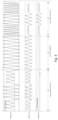
FIG. 4 is a communication waveform diagram of a communication system of the present invention; -
FIG. 5 is a schematic view showing the position and shape of a coil according to Example One of the present invention; -
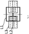
FIG. 6 is a schematic view showing the position and shape of a coil according to Example Two of the present invention; -
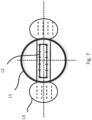
FIG. 7 is a schematic view showing the position and shape of a coil according to Example Three, not encompassed by the claimed invention. - In order to facilitate a further understanding of the present invention, it will be further illustrated below with reference to the accompanying drawings.
- As shown in the drawings, the present invention firstly discloses a communication system of an implantable device, comprising: an external unit and an implantable unit, wherein the external unit and the implantable unit realize charging and bidirectional signal transmitting of the external unit to the implantable unit by a wireless signal. In which, the external unit comprises a digital signal processing unit, a power transmission unit and a receiver and demodulation unit, and the internal unit comprises a stimulation module and a signal receiver and transmission unit. The power transmission unit comprises a first coupling coil L1, the first coupling coil is configured to transmit a signal to the internal unit, the signal receiver unit comprises a second coupling coil L2, and the second coupling coil L2 is configured to receive the signal transmitted from the external unit and transmit a signal to the external unit, the receiver and modulation unit comprises a third coupling coil L3, and the third coupling coil is configured to receive the signal transmitted from the implantable unit. The third coupling coil L3 is disposed between the first coupling coil L1 and the second coupling coil L2.
- During the signal transmission, the external unit transmits a signal to the internal unit via coupling between the first coupling coil and the second coupling coil in the internal unit, and the internal unit receives the signal and achieves charging.
- Since the size of the second coupling coil L2 in the internal unit is generally small, in order for the internal unit to obtain more energy, it is necessary to increase the transmission power of the external unit, and it is necessary to increase the size of the first coupling coil in the external unit, and increase the coupling coefficient k12. If the first coupling coil is continuously used to receive the reverse signal transmitted from the internal unit, the reverse coupling coefficient k21 will be small, when the reverse data transmission is transmitted, there is a signal with an amplitude modulation on the second coupling coil, and a corresponding signal envelope (amplitude VPP_backward) appears on the L1 coil by load reflection, however, since coupling coefficient k21 is very small, the envelop amplitude of useful signal seen on the L1 will be very small, and in some severe environments, the signal will be completely submerged by the signal and the noise from L1, causing the receiver and demodulation unit in the external unit to fail to receive the useful signal, resulting in failure of the reverse data work of the entire system.
- The present invention uses the third coupling coil L3 to receive the reverse signal, during the signal transmission, the center position of the first coupling coil L1 is aligned with the center position of the third coupling coil L3, and the third coupling coil L3 has a symmetrical shape, so that magnetic induction currents of the first coupling coil L1 coupled through the third coupling coil L3 are canceled each other out.
- In general, the size of the first coupling coil L1 is larger than the size of the second coupling coil L2, and the projection of the second coupling coil L2 and the projection of the first coupling coil L1 overlap, ensuring the signal forwardly transmitted by the first coupling coil L1 will be effectively received by the second coupling coil L2 disposed in the body. Furthermore, the second coupling coil L2 is in the projection of the first coupling coil L1 and the third coupling coil L3, the coupling effect of the first coupling coil L1 and the second coupling coil L2 is better.
- In addition, a signal shielding device for preventing interference with communications among the first coupling coil L1, the second coupling coil L2 and the third coupling coil L3 is further disposed outside the first coupling coil L1, and such signal shielding device can make the communications among the coupling coils more stable.
- In order to prevent the reverse signal transmission from being affected by the first coupling coil and the second coupling coil, the position and shape setting of the third coupling coil can be implemented in various embodiments, and several are listed below.
- The third coupling coil L3 comprises two symmetrical parts, the coils on the two symmetrical parts are arranged to cross each other through a symmetric center, its cross point overlaps with the center of the first coupling coil, there is an offset between the center cross point position of the second coupling coil L2 and the third coupling coil L3, and positive and negative currents generated on the third coupling coil are canceled each other out, when the first coupling coil is coupled, and when the second coupling coil is coupled, the third coupling coil can fully receive the signal. In this Example, the first coupling coil is a toroidal coil, and the two symmetrical parts of the third coupling coil are both loop coils with a curvature.
- The third coupling coil L3 comprises two symmetrical parts, the coils on the two symmetrical parts are arranged to cross each other through a symmetric center, its cross point overlaps with the center of the first coupling coil, there is an offset between the center cross point position of the second coupling coil L2 and the third coupling coil L3, and positive and negative currents generated on the third coupling coil are canceled each other out, when the first coupling coil is coupled, and when the second coupling coil is coupled, the third coupling coil can fully receive the signal. The first coupling coil is a square loop coil, and the two symmetrical parts of the third coupling coil are both square loop coils.
- The third coupling coil L3 comprises a region S 1 overlapping with the projection of the first coupling coil L1 and a region S2 not overlapping with the projection of the first coupling coil L1; through detecting and testing, a position of the third coupling coil relative to the first coupling coil is properly placed, so that the positive and negative magnetic fluxes passing through two regions of the third coupling coil L3 are canceled each other out, when the first coupling coil L1 is coupled. The third coupling coil L3 comprises an intermediate portion coil having a straight shape and end coils connected to the two ends of the intermediate portion, wherein the intermediate portion coil overlaps with the first coupling coil, and the two end coils does not overlap with the first coupling coil. When the signal is transmitted in a direction from the second coupling coil L2, the positive and negative magnetic fluxes passing through the overlap region S 1 and the non-overlap region S2 of the third coupling coil are equal, therefore when the signal is reversely transmitted, the coupling of the second coupling coil and the first coupling coil does not cause interference to the signal received by the third coupling coil.
- The aforementioned examples are merely preferred examples of the present invention, which are not intended to limit the present invention.
Claims (5)
- A communication system of an implantable device, comprising an external unit and an implantable unit, and wherein the external unit and the implantable unit realize charging and bidirectional signal transmission of the external unit to the implantable unit by a wireless signal,wherein the external unit comprises a digital signal processing unit, a power transmission unit and a receiver and demodulation unit, the implantable unit comprises a stimulation module and a signal receiver and transmission unit, the power transmission unit of the external unit comprises a first coupling coil L1, the first coupling coil L1 is configured to transmit a signal to the implantable unit, the signal receiver unit of the implantable unit comprises a second coupling coil L2, the second coupling coil L2 is configured to receive the signal from the external unit and transmit a signal to the external unit, the receiver and modulation unit of the external device comprises a third coupling coil L3, and the third coupling coil L3 is configured to receive the signal from the implantable unit,characterized in that,the third coupling coil L3 comprises two symmetrical parts, the coils on the two symmetrical parts are arranged to cross each other through a symmetric center, a cross point thereof overlaps with a center of the first coupling coil L1, there is an offset between a center of the second coupling coil L2 and a center cross point position of the third coupling coil L3, and a positive and negative current generated by coupling the first coupling coil L1 through the third coupling coil L3 cancel each other out, and a size of the first coupling coil L1 is larger than a size of the second coupling coil L2, the second coupling coil L2 is in the projections of the first coupling coil L1 and the third coupling coil L3.
- The communication system of the implantable device according to claim 1, characterized in that, the third coupling coil L3 is disposed between the first coupling coil L1 and the second coupling coil L2.
- The communication system of the implantable device according to claim 1, characterized in that, a center position of the first coupling coil L1 is aligned with a center position of the third coupling coil L3, and the third coupling coil L3 has a symmetrical shape, the magnetic induction current of the first coupling coil L1 coupled through the third coupling coil L3 are canceled each other out.
- The communication system of the implantable device according to claim 1, characterized in that, the first coupling coil L1 is a toroidal coil, and the two symmetrical parts of the third coupling coil L3 are both loop coils with a curvature.
- The communication system of the implantable device according to claim 1, characterized in that, the first coupling coil L1 is a square loop coil, and the two symmetrical parts of the third coupling coil L3 are both square loop coils.
Applications Claiming Priority (2)
| Application Number | Priority Date | Filing Date | Title |
|---|---|---|---|
| CN201810357705.7A CN108390701A (en) | 2018-04-20 | 2018-04-20 | A kind of implantation device talk system |
| PCT/CN2018/123078 WO2019200960A1 (en) | 2018-04-20 | 2018-12-24 | Communication system for implant device |
Publications (3)
| Publication Number | Publication Date |
|---|---|
| EP3584950A1 EP3584950A1 (en) | 2019-12-25 |
| EP3584950A4 EP3584950A4 (en) | 2020-04-15 |
| EP3584950B1 true EP3584950B1 (en) | 2023-08-02 |
Family
ID=63065610
Family Applications (1)
| Application Number | Title | Priority Date | Filing Date |
|---|---|---|---|
| EP18906705.1A Active EP3584950B1 (en) | 2018-04-20 | 2018-12-24 | Communication system for implant device |
Country Status (8)
| Country | Link |
|---|---|
| US (1) | US20200353270A1 (en) |
| EP (1) | EP3584950B1 (en) |
| JP (1) | JP6854023B2 (en) |
| CN (1) | CN108390701A (en) |
| AU (1) | AU2018393125B2 (en) |
| ES (1) | ES2962990T3 (en) |
| HU (1) | HUE063606T2 (en) |
| WO (1) | WO2019200960A1 (en) |
Families Citing this family (4)
| Publication number | Priority date | Publication date | Assignee | Title |
|---|---|---|---|---|
| CN108390701A (en) * | 2018-04-20 | 2018-08-10 | 杭州暖芯迦电子科技有限公司 | A kind of implantation device talk system |
| CN110557127B (en) * | 2019-09-27 | 2021-09-07 | 中国科学院深圳先进技术研究院 | Multi-coil antenna systems and implantable medical devices |
| CN113964957B (en) * | 2021-11-18 | 2023-12-05 | 重庆前卫无线电能传输研究院有限公司 | A sleeve-type wireless energy signal transmission coupling mechanism and system |
| CN116780787B (en) * | 2023-08-18 | 2023-10-27 | 航天泰心科技有限公司 | Wireless energy supply receiving device implanted in body and wireless power transmission system |
Family Cites Families (11)
| Publication number | Priority date | Publication date | Assignee | Title |
|---|---|---|---|---|
| US5630835A (en) * | 1995-07-24 | 1997-05-20 | Cardiac Control Systems, Inc. | Method and apparatus for the suppression of far-field interference signals for implantable device data transmission systems |
| JP3528367B2 (en) * | 1995-09-30 | 2004-05-17 | ソニーケミカル株式会社 | Antenna for reader / writer |
| US8548597B2 (en) * | 2006-09-29 | 2013-10-01 | Second Sight Medical Products, Inc. | External coil assembly for implantable medical prostheses |
| CN101856540A (en) * | 2009-04-10 | 2010-10-13 | 张希华 | Implanted telemetering stimulating system based on wireless power transmission and two-way communication |
| US20120244802A1 (en) * | 2011-03-24 | 2012-09-27 | Lei Feng | On chip inductor |
| CN102157989A (en) * | 2011-03-28 | 2011-08-17 | 东南大学 | Closed loop wireless energy supply system for implantable medical electronic device |
| US10603501B2 (en) * | 2016-06-15 | 2020-03-31 | Boston Scientific Neuromodulation Corporation | External charger for an implantable medical device having at least one sense coil concentric with a charging coil for determining position |
| CN107482790B (en) * | 2017-08-04 | 2019-07-02 | 河南师范大学 | Design method of high-efficiency forward parallel wireless power supply system |
| CN107769812B (en) * | 2017-10-31 | 2019-10-15 | 乐普医学电子仪器股份有限公司 | A kind of wireless telecommunication system for implantable medical devices |
| CN208386541U (en) * | 2018-04-20 | 2019-01-15 | 杭州暖芯迦电子科技有限公司 | A kind of implantation device talk system |
| CN108390701A (en) * | 2018-04-20 | 2018-08-10 | 杭州暖芯迦电子科技有限公司 | A kind of implantation device talk system |
-
2018
- 2018-04-20 CN CN201810357705.7A patent/CN108390701A/en active Pending
- 2018-12-24 ES ES18906705T patent/ES2962990T3/en active Active
- 2018-12-24 US US16/640,718 patent/US20200353270A1/en not_active Abandoned
- 2018-12-24 AU AU2018393125A patent/AU2018393125B2/en active Active
- 2018-12-24 WO PCT/CN2018/123078 patent/WO2019200960A1/en not_active Ceased
- 2018-12-24 HU HUE18906705A patent/HUE063606T2/en unknown
- 2018-12-24 JP JP2019518266A patent/JP6854023B2/en active Active
- 2018-12-24 EP EP18906705.1A patent/EP3584950B1/en active Active
Also Published As
| Publication number | Publication date |
|---|---|
| CN108390701A (en) | 2018-08-10 |
| JP6854023B2 (en) | 2021-04-07 |
| AU2018393125B2 (en) | 2021-08-12 |
| HUE063606T2 (en) | 2024-01-28 |
| EP3584950A1 (en) | 2019-12-25 |
| AU2018393125A1 (en) | 2019-11-07 |
| EP3584950A4 (en) | 2020-04-15 |
| ES2962990T3 (en) | 2024-03-22 |
| US20200353270A1 (en) | 2020-11-12 |
| JP2020520130A (en) | 2020-07-02 |
| WO2019200960A1 (en) | 2019-10-24 |
Similar Documents
| Publication | Publication Date | Title |
|---|---|---|
| AU2018393125B2 (en) | Communication system of implantable device | |
| US4542532A (en) | Dual-antenna transceiver | |
| US9634439B2 (en) | Contactless plug connector and contactless plug connector system | |
| US5548815A (en) | Inductive radio communication system | |
| EP3136614B1 (en) | Near-field antenna system | |
| EP2347522B1 (en) | Electronic devices and methods that communicate via transferjet and nfc transmitter and receiver pairing | |
| WO2020040905A3 (en) | Wireless charging system with multiple communications modes | |
| US20230369916A1 (en) | Wireless power transmission apparatus, wireless power reception apparatus, and wireless charging system | |
| US5630835A (en) | Method and apparatus for the suppression of far-field interference signals for implantable device data transmission systems | |
| US10790083B2 (en) | Wireless charger having electromagnetic shielding function | |
| EP1202775A1 (en) | A medical system having improved telemetry | |
| JP5558895B2 (en) | Hearing aid device for wireless data transmission with neck strap with integrated antenna and method for wireless data transmission | |
| WO2016147695A1 (en) | Connector device and communication system | |
| US4148036A (en) | Magnetic quadrapole antenna | |
| CN208386541U (en) | A kind of implantation device talk system | |
| CN112731540A (en) | Single-transmitting and double-receiving zero-magnetic-flux detection coil | |
| EP3204986B1 (en) | Device for providing wireless energy transfer | |
| GB2317993A (en) | Antenna switching means for portable radio apparatus | |
| CN111448630A (en) | Coil design for wireless power transfer | |
| US20220416845A1 (en) | Nfc antenna | |
| JP6760326B2 (en) | Communication assistance unit | |
| US20170149268A1 (en) | Communication device | |
| JP2000050511A (en) | Connector device for electric vehicle charging | |
| WO2026087149A1 (en) | Communication method and medical communication system | |
| JP2006157230A (en) | Data carrier circuit |
Legal Events
| Date | Code | Title | Description |
|---|---|---|---|
| STAA | Information on the status of an ep patent application or granted ep patent |
Free format text: STATUS: UNKNOWN |
|
| STAA | Information on the status of an ep patent application or granted ep patent |
Free format text: STATUS: THE INTERNATIONAL PUBLICATION HAS BEEN MADE |
|
| PUAI | Public reference made under article 153(3) epc to a published international application that has entered the european phase |
Free format text: ORIGINAL CODE: 0009012 |
|
| STAA | Information on the status of an ep patent application or granted ep patent |
Free format text: STATUS: REQUEST FOR EXAMINATION WAS MADE |
|
| 17P | Request for examination filed |
Effective date: 20190826 |
|
| AK | Designated contracting states |
Kind code of ref document: A1 Designated state(s): AL AT BE BG CH CY CZ DE DK EE ES FI FR GB GR HR HU IE IS IT LI LT LU LV MC MK MT NL NO PL PT RO RS SE SI SK SM TR |
|
| AX | Request for extension of the european patent |
Extension state: BA ME |
|
| R17P | Request for examination filed (corrected) |
Effective date: 20190826 |
|
| A4 | Supplementary search report drawn up and despatched |
Effective date: 20200313 |
|
| RIC1 | Information provided on ipc code assigned before grant |
Ipc: H04B 5/00 20060101AFI20200309BHEP Ipc: H02J 50/12 20160101ALI20200309BHEP Ipc: A61N 1/00 20060101ALI20200309BHEP Ipc: A61N 1/36 20060101ALI20200309BHEP |
|
| STAA | Information on the status of an ep patent application or granted ep patent |
Free format text: STATUS: EXAMINATION IS IN PROGRESS |
|
| 17Q | First examination report despatched |
Effective date: 20210120 |
|
| DAV | Request for validation of the european patent (deleted) | ||
| DAX | Request for extension of the european patent (deleted) | ||
| GRAP | Despatch of communication of intention to grant a patent |
Free format text: ORIGINAL CODE: EPIDOSNIGR1 |
|
| STAA | Information on the status of an ep patent application or granted ep patent |
Free format text: STATUS: GRANT OF PATENT IS INTENDED |
|
| INTG | Intention to grant announced |
Effective date: 20230323 |
|
| GRAS | Grant fee paid |
Free format text: ORIGINAL CODE: EPIDOSNIGR3 |
|
| GRAA | (expected) grant |
Free format text: ORIGINAL CODE: 0009210 |
|
| STAA | Information on the status of an ep patent application or granted ep patent |
Free format text: STATUS: THE PATENT HAS BEEN GRANTED |
|
| AK | Designated contracting states |
Kind code of ref document: B1 Designated state(s): AL AT BE BG CH CY CZ DE DK EE ES FI FR GB GR HR HU IE IS IT LI LT LU LV MC MK MT NL NO PL PT RO RS SE SI SK SM TR |
|
| REG | Reference to a national code |
Ref country code: GB Ref legal event code: FG4D |
|
| REG | Reference to a national code |
Ref country code: CH Ref legal event code: EP |
|
| REG | Reference to a national code |
Ref country code: DE Ref legal event code: R096 Ref document number: 602018054810 Country of ref document: DE |
|
| REG | Reference to a national code |
Ref country code: IE Ref legal event code: FG4D |
|
| REG | Reference to a national code |
Ref country code: SE Ref legal event code: TRGR |
|
| REG | Reference to a national code |
Ref country code: LT Ref legal event code: MG9D |
|
| REG | Reference to a national code |
Ref country code: NL Ref legal event code: MP Effective date: 20230802 |
|
| REG | Reference to a national code |
Ref country code: AT Ref legal event code: MK05 Ref document number: 1595981 Country of ref document: AT Kind code of ref document: T Effective date: 20230802 |
|
| PG25 | Lapsed in a contracting state [announced via postgrant information from national office to epo] |
Ref country code: GR Free format text: LAPSE BECAUSE OF FAILURE TO SUBMIT A TRANSLATION OF THE DESCRIPTION OR TO PAY THE FEE WITHIN THE PRESCRIBED TIME-LIMIT Effective date: 20231103 |
|
| PG25 | Lapsed in a contracting state [announced via postgrant information from national office to epo] |
Ref country code: IS Free format text: LAPSE BECAUSE OF FAILURE TO SUBMIT A TRANSLATION OF THE DESCRIPTION OR TO PAY THE FEE WITHIN THE PRESCRIBED TIME-LIMIT Effective date: 20231202 |
|
| REG | Reference to a national code |
Ref country code: HU Ref legal event code: AG4A Ref document number: E063606 Country of ref document: HU |
|
| PG25 | Lapsed in a contracting state [announced via postgrant information from national office to epo] |
Ref country code: RS Free format text: LAPSE BECAUSE OF FAILURE TO SUBMIT A TRANSLATION OF THE DESCRIPTION OR TO PAY THE FEE WITHIN THE PRESCRIBED TIME-LIMIT Effective date: 20230802 Ref country code: PT Free format text: LAPSE BECAUSE OF FAILURE TO SUBMIT A TRANSLATION OF THE DESCRIPTION OR TO PAY THE FEE WITHIN THE PRESCRIBED TIME-LIMIT Effective date: 20231204 Ref country code: NO Free format text: LAPSE BECAUSE OF FAILURE TO SUBMIT A TRANSLATION OF THE DESCRIPTION OR TO PAY THE FEE WITHIN THE PRESCRIBED TIME-LIMIT Effective date: 20231102 Ref country code: NL Free format text: LAPSE BECAUSE OF FAILURE TO SUBMIT A TRANSLATION OF THE DESCRIPTION OR TO PAY THE FEE WITHIN THE PRESCRIBED TIME-LIMIT Effective date: 20230802 Ref country code: LV Free format text: LAPSE BECAUSE OF FAILURE TO SUBMIT A TRANSLATION OF THE DESCRIPTION OR TO PAY THE FEE WITHIN THE PRESCRIBED TIME-LIMIT Effective date: 20230802 Ref country code: LT Free format text: LAPSE BECAUSE OF FAILURE TO SUBMIT A TRANSLATION OF THE DESCRIPTION OR TO PAY THE FEE WITHIN THE PRESCRIBED TIME-LIMIT Effective date: 20230802 Ref country code: IS Free format text: LAPSE BECAUSE OF FAILURE TO SUBMIT A TRANSLATION OF THE DESCRIPTION OR TO PAY THE FEE WITHIN THE PRESCRIBED TIME-LIMIT Effective date: 20231202 Ref country code: HR Free format text: LAPSE BECAUSE OF FAILURE TO SUBMIT A TRANSLATION OF THE DESCRIPTION OR TO PAY THE FEE WITHIN THE PRESCRIBED TIME-LIMIT Effective date: 20230802 Ref country code: GR Free format text: LAPSE BECAUSE OF FAILURE TO SUBMIT A TRANSLATION OF THE DESCRIPTION OR TO PAY THE FEE WITHIN THE PRESCRIBED TIME-LIMIT Effective date: 20231103 Ref country code: FI Free format text: LAPSE BECAUSE OF FAILURE TO SUBMIT A TRANSLATION OF THE DESCRIPTION OR TO PAY THE FEE WITHIN THE PRESCRIBED TIME-LIMIT Effective date: 20230802 Ref country code: AT Free format text: LAPSE BECAUSE OF FAILURE TO SUBMIT A TRANSLATION OF THE DESCRIPTION OR TO PAY THE FEE WITHIN THE PRESCRIBED TIME-LIMIT Effective date: 20230802 |
|
| PG25 | Lapsed in a contracting state [announced via postgrant information from national office to epo] |
Ref country code: PL Free format text: LAPSE BECAUSE OF FAILURE TO SUBMIT A TRANSLATION OF THE DESCRIPTION OR TO PAY THE FEE WITHIN THE PRESCRIBED TIME-LIMIT Effective date: 20230802 |
|
| REG | Reference to a national code |
Ref country code: ES Ref legal event code: FG2A Ref document number: 2962990 Country of ref document: ES Kind code of ref document: T3 Effective date: 20240322 |
|
| PG25 | Lapsed in a contracting state [announced via postgrant information from national office to epo] |
Ref country code: SM Free format text: LAPSE BECAUSE OF FAILURE TO SUBMIT A TRANSLATION OF THE DESCRIPTION OR TO PAY THE FEE WITHIN THE PRESCRIBED TIME-LIMIT Effective date: 20230802 Ref country code: RO Free format text: LAPSE BECAUSE OF FAILURE TO SUBMIT A TRANSLATION OF THE DESCRIPTION OR TO PAY THE FEE WITHIN THE PRESCRIBED TIME-LIMIT Effective date: 20230802 Ref country code: EE Free format text: LAPSE BECAUSE OF FAILURE TO SUBMIT A TRANSLATION OF THE DESCRIPTION OR TO PAY THE FEE WITHIN THE PRESCRIBED TIME-LIMIT Effective date: 20230802 Ref country code: DK Free format text: LAPSE BECAUSE OF FAILURE TO SUBMIT A TRANSLATION OF THE DESCRIPTION OR TO PAY THE FEE WITHIN THE PRESCRIBED TIME-LIMIT Effective date: 20230802 Ref country code: CZ Free format text: LAPSE BECAUSE OF FAILURE TO SUBMIT A TRANSLATION OF THE DESCRIPTION OR TO PAY THE FEE WITHIN THE PRESCRIBED TIME-LIMIT Effective date: 20230802 Ref country code: SK Free format text: LAPSE BECAUSE OF FAILURE TO SUBMIT A TRANSLATION OF THE DESCRIPTION OR TO PAY THE FEE WITHIN THE PRESCRIBED TIME-LIMIT Effective date: 20230802 |
|
| REG | Reference to a national code |
Ref country code: DE Ref legal event code: R097 Ref document number: 602018054810 Country of ref document: DE |
|
| PLBE | No opposition filed within time limit |
Free format text: ORIGINAL CODE: 0009261 |
|
| STAA | Information on the status of an ep patent application or granted ep patent |
Free format text: STATUS: NO OPPOSITION FILED WITHIN TIME LIMIT |
|
| 26N | No opposition filed |
Effective date: 20240503 |
|
| PG25 | Lapsed in a contracting state [announced via postgrant information from national office to epo] |
Ref country code: SI Free format text: LAPSE BECAUSE OF FAILURE TO SUBMIT A TRANSLATION OF THE DESCRIPTION OR TO PAY THE FEE WITHIN THE PRESCRIBED TIME-LIMIT Effective date: 20230802 |
|
| PG25 | Lapsed in a contracting state [announced via postgrant information from national office to epo] |
Ref country code: BG Free format text: LAPSE BECAUSE OF FAILURE TO SUBMIT A TRANSLATION OF THE DESCRIPTION OR TO PAY THE FEE WITHIN THE PRESCRIBED TIME-LIMIT Effective date: 20230802 |
|
| PG25 | Lapsed in a contracting state [announced via postgrant information from national office to epo] |
Ref country code: BG Free format text: LAPSE BECAUSE OF FAILURE TO SUBMIT A TRANSLATION OF THE DESCRIPTION OR TO PAY THE FEE WITHIN THE PRESCRIBED TIME-LIMIT Effective date: 20230802 |
|
| PG25 | Lapsed in a contracting state [announced via postgrant information from national office to epo] |
Ref country code: CY Free format text: LAPSE BECAUSE OF FAILURE TO SUBMIT A TRANSLATION OF THE DESCRIPTION OR TO PAY THE FEE WITHIN THE PRESCRIBED TIME-LIMIT; INVALID AB INITIO Effective date: 20181224 |
|
| PG25 | Lapsed in a contracting state [announced via postgrant information from national office to epo] |
Ref country code: TR Free format text: LAPSE BECAUSE OF FAILURE TO SUBMIT A TRANSLATION OF THE DESCRIPTION OR TO PAY THE FEE WITHIN THE PRESCRIBED TIME-LIMIT Effective date: 20230802 |
|
| PGFP | Annual fee paid to national office [announced via postgrant information from national office to epo] |
Ref country code: LU Payment date: 20251127 Year of fee payment: 8 |
|
| REG | Reference to a national code |
Ref country code: CH Ref legal event code: U11 Free format text: ST27 STATUS EVENT CODE: U-0-0-U10-U11 (AS PROVIDED BY THE NATIONAL OFFICE) Effective date: 20260101 |
|
| PGFP | Annual fee paid to national office [announced via postgrant information from national office to epo] |
Ref country code: GB Payment date: 20251229 Year of fee payment: 8 |
|
| PGFP | Annual fee paid to national office [announced via postgrant information from national office to epo] |
Ref country code: MC Payment date: 20251126 Year of fee payment: 8 |
|
| PGFP | Annual fee paid to national office [announced via postgrant information from national office to epo] |
Ref country code: IT Payment date: 20251210 Year of fee payment: 8 |
|
| PGFP | Annual fee paid to national office [announced via postgrant information from national office to epo] |
Ref country code: HU Payment date: 20251124 Year of fee payment: 8 Ref country code: FR Payment date: 20251230 Year of fee payment: 8 |
|
| PGFP | Annual fee paid to national office [announced via postgrant information from national office to epo] |
Ref country code: BE Payment date: 20251226 Year of fee payment: 8 |
|
| PGFP | Annual fee paid to national office [announced via postgrant information from national office to epo] |
Ref country code: SE Payment date: 20251218 Year of fee payment: 8 |
|
| PGFP | Annual fee paid to national office [announced via postgrant information from national office to epo] |
Ref country code: IE Payment date: 20251126 Year of fee payment: 8 |
|
| PGFP | Annual fee paid to national office [announced via postgrant information from national office to epo] |
Ref country code: ES Payment date: 20260112 Year of fee payment: 8 |
|
| PGFP | Annual fee paid to national office [announced via postgrant information from national office to epo] |
Ref country code: DE Payment date: 20251231 Year of fee payment: 8 |
|
| PGFP | Annual fee paid to national office [announced via postgrant information from national office to epo] |
Ref country code: CH Payment date: 20260101 Year of fee payment: 8 |