EP3584917A1 - Two-stage switch power supply - Google Patents
Two-stage switch power supply Download PDFInfo
- Publication number
- EP3584917A1 EP3584917A1 EP18771684.0A EP18771684A EP3584917A1 EP 3584917 A1 EP3584917 A1 EP 3584917A1 EP 18771684 A EP18771684 A EP 18771684A EP 3584917 A1 EP3584917 A1 EP 3584917A1
- Authority
- EP
- European Patent Office
- Prior art keywords
- voltage
- module
- resistor
- control
- power supply
- Prior art date
- Legal status (The legal status is an assumption and is not a legal conclusion. Google has not performed a legal analysis and makes no representation as to the accuracy of the status listed.)
- Granted
Links
Images

Classifications
-
- H—ELECTRICITY
- H02—GENERATION; CONVERSION OR DISTRIBUTION OF ELECTRIC POWER
- H02M—APPARATUS FOR CONVERSION BETWEEN AC AND AC, BETWEEN AC AND DC, OR BETWEEN DC AND DC, AND FOR USE WITH MAINS OR SIMILAR POWER SUPPLY SYSTEMS; CONVERSION OF DC OR AC INPUT POWER INTO SURGE OUTPUT POWER; CONTROL OR REGULATION THEREOF
- H02M1/00—Details of apparatus for conversion
- H02M1/32—Means for protecting converters other than automatic disconnection
-
- H—ELECTRICITY
- H02—GENERATION; CONVERSION OR DISTRIBUTION OF ELECTRIC POWER
- H02M—APPARATUS FOR CONVERSION BETWEEN AC AND AC, BETWEEN AC AND DC, OR BETWEEN DC AND DC, AND FOR USE WITH MAINS OR SIMILAR POWER SUPPLY SYSTEMS; CONVERSION OF DC OR AC INPUT POWER INTO SURGE OUTPUT POWER; CONTROL OR REGULATION THEREOF
- H02M1/00—Details of apparatus for conversion
- H02M1/36—Means for starting or stopping converters
-
- H—ELECTRICITY
- H02—GENERATION; CONVERSION OR DISTRIBUTION OF ELECTRIC POWER
- H02M—APPARATUS FOR CONVERSION BETWEEN AC AND AC, BETWEEN AC AND DC, OR BETWEEN DC AND DC, AND FOR USE WITH MAINS OR SIMILAR POWER SUPPLY SYSTEMS; CONVERSION OF DC OR AC INPUT POWER INTO SURGE OUTPUT POWER; CONTROL OR REGULATION THEREOF
- H02M1/00—Details of apparatus for conversion
- H02M1/0003—Details of control, feedback or regulation circuits
- H02M1/0006—Arrangements for supplying an adequate voltage to the control circuit of converters
-
- H—ELECTRICITY
- H02—GENERATION; CONVERSION OR DISTRIBUTION OF ELECTRIC POWER
- H02M—APPARATUS FOR CONVERSION BETWEEN AC AND AC, BETWEEN AC AND DC, OR BETWEEN DC AND DC, AND FOR USE WITH MAINS OR SIMILAR POWER SUPPLY SYSTEMS; CONVERSION OF DC OR AC INPUT POWER INTO SURGE OUTPUT POWER; CONTROL OR REGULATION THEREOF
- H02M1/00—Details of apparatus for conversion
- H02M1/0067—Converter structures employing plural converter units, other than for parallel operation of the units on a single load
- H02M1/007—Plural converter units in cascade
-
- H—ELECTRICITY
- H02—GENERATION; CONVERSION OR DISTRIBUTION OF ELECTRIC POWER
- H02M—APPARATUS FOR CONVERSION BETWEEN AC AND AC, BETWEEN AC AND DC, OR BETWEEN DC AND DC, AND FOR USE WITH MAINS OR SIMILAR POWER SUPPLY SYSTEMS; CONVERSION OF DC OR AC INPUT POWER INTO SURGE OUTPUT POWER; CONTROL OR REGULATION THEREOF
- H02M1/00—Details of apparatus for conversion
- H02M1/32—Means for protecting converters other than automatic disconnection
- H02M1/325—Means for protecting converters other than automatic disconnection with means for allowing continuous operation despite a fault, i.e. fault tolerant converters
Definitions
- the present invention relates to a technical field of switch power supply, and in particular, to a two stage switch power supply.
- the two-stage switch power supply in prior art includes a first control module, a second control module, a first conversion module, and a second conversion module, wherein the first control module and the second control module respectively control the first conversion module and the second conversion module.
- the first conversion module outputs a voltage to the second conversion module.
- the second conversion module When the second conversion module outputs to bring in a load, the output voltage of the first conversion module is rapidly decreased, causing the entire switch to be in an intermittent working state.
- increasing the output voltage of the first conversion module will increase the consumption of the switch power supply.
- increasing the output voltage of the first conversion module in order to prevent the switch power supply from being in an intermittent working state causes an increase in the consumption of the switch power supply.
- the object of the present invention is to provide a two-stage switch power supply capable of solving the problem existing in prior art, that is, increasing the output voltage of the first conversion module in order to prevent the switch power supply from being in an intermittent working state causes an increase in the consumption of the switch power supply.
- a first aspect of the present invention provides a two-stage switch power supply which includes an input rectification module, a first control module, a first conversion module, a second control module, a second conversion module, and a voltage limiting switch module; an output end of the input rectification module is connected to a voltage input end of the first control module and a voltage input end of the first conversion module, a signal output end of the first control module is connected to a control end of the first conversion module, a voltage output end of the first conversion module is connected to a first voltage input end of the second conversion module, a first voltage input end of the voltage limiting switch module, and a voltage input end of the second control module, a second voltage input end of the voltage limiting switch module is connected to a control end of the second control module, an output end of the second control module is connected to a second voltage input end and a third voltage input end of the second conversion module; the input rectification module performs rectification and filtering on an input voltage and then outputs a
- the present invention provides a two-stage switch power supply which, by providing a voltage limiting delay start module to perform a delay control on the start of a second-stage control module during the starting process, avoids the problem that the switch power supply is in an intermittent working state due to a low voltage output by the first conversion module, and achieves a rapid start with high efficiency and low loss. Moreover, the structure is simple, and the overall cost is low.
- the two-stage switch power supply 10 includes an input rectification module 101, a first control module 102, a first conversion module 103, a second control module 106, a second conversion module 104, and a voltage limiting switch module 105; an output end of the input rectification module 101 is connected to a voltage input end of the first control module 102 and a voltage input end of the first conversion module 103, a signal output end of the first control module 102 is connected to a control end of the first conversion module 103, a voltage output end of the first conversion module 103 is connected to a voltage input end of the second conversion module 104, a first voltage input end of the voltage limiting switch module 105, and a voltage input end of the second control module 106, a second voltage input end of the voltage limiting switch module 105 is connected to a control end of the second control module 106, an output end of the second control module 106 is connected to a
- the input rectification module 101 is configured to perform rectification and filtering on an input alternating current and then to supply power to the first control module 102 and the first conversion module 103.
- the first control module 102 starts and controls the first conversion module 103 to work.
- the first conversion module 103 outputs a voltage to supply power to the first control module 102 on the one hand, and to supply power to the second conversion module 104, the voltage limiting switch module 105, and the second control module 106 on the other hand.
- the voltage limiting switch module 105 does not immediately control the second control module 106 to work until the voltage output by the first conversion module 103 reaches a preset voltage, and then the second control module 106 controls the second conversion module 104 to start working.
- the output end of the second conversion module 104 is connected to the load, since the output voltage of the first conversion module 103 is high, it does not cause too much power supplied to the load to make the first control module 102 be in an intermittent working state.
- the voltage limiting switch module 105 may be a delay module consisting of discrete components, or may be a delay voltage limiting chip.
- the voltage limiting switch module 105 is in an on state connected to the ground when the bus voltage has not reached the preset voltage, and the control end of the second control module 106 is connected to the ground; the voltage limiting switch module 105 is disconnected from the ground when the bus voltage reaches the preset voltage, and the second control module 106 charges the voltage limiting switch module 105 through its control end so as to make the second control module 106 reach a working state.
- the second control module 106 may be a control chip.
- the working principle of the control chip is that a voltage is output to the voltage limiting switch module 105 through a soft start function pin, and when the voltage value stored on the voltage limiting switch module 105 reaches a preset value, the control chip is made to work.
- the control chip In order to prevent the control chip from working when the output voltage of the first conversion module 103 is small, it is in an on state connected to the ground when the bus voltage has not reached the preset voltage, and the soft start function pin of the control chip is connected to the ground. At this time, the voltage value stored on the voltage limiting switch module 105 is 0, and the control chip does not work.
- the control chip charges the voltage limiting switch module 105 through the soft start function pin so as to make the second control module 106 reach a working state.
- the voltage limiting switch module 105 includes a voltage limiting device 501, a first voltage dividing device 1502, a second voltage dividing device 1503, a switch tube 1504, and an energy storage device 1505, wherein a first end of the voltage limiting device 1501 is the voltage input end of the voltage limiting switch module 105, a second end of the voltage limiting device 1501 is connected to a first end of the first voltage dividing device 1502, a second end of the first voltage dividing device 1502 is connected to a control end of the switch tube 1504 and a first end of the second voltage dividing device 1503, an input end of the switch tube 1504 is connected to the control end of the second control module 106 and a first end of the energy storage device 1505, an output end of the switch tube 1504, a second end of the second voltage dividing device 1503, and a second end of the energy storage device 1505 are connected to the ground together; the voltage limiting device 1501 is in an off state when the bus voltage has not reached the prese
- the voltage limiting device 1504 may be a voltage stabilizing tube, and a cathode and an anode of the voltage stabilizing tube are the first end and the second end of the voltage limiting device.
- the voltage limiting device 1504 may also be a chip with a voltage limiting function, and it is not limited herein.
- the switch tube 1504 is a PNP type triode, and a collector, an emitter, and a base of the PNP type triode are respectively the output end, the input end, and the control end of the switch tube.
- the switch tube 1504 is a P type MOS transistor, and a drain, a source, and a gate of the P type MOS transistor are respectively the output end, the input end, and the control end of the switch tube.
- the first conversion module 103 stops working, the voltage limiting device 1501 is in an off state, and the switch tube 1504 is in an on state to discharge the energy storage device to the ground.
- a rapid reset of the soft start function pin of the control chip is achieved by discharging the energy storage device to the ground, so that the soft start function pin has a soft start function in the next start process.
- the first control module 102 includes a power supply module 1201 and a first control chip 1202, a voltage input end of the power supply module 1201 is a voltage input end of the first control module 102, a voltage output end of the power supply module 1201 is connected to the voltage input end of the first control chip 1202, and a voltage output end of the first control chip 1202 is a voltage output end of the first control module 102; the power supply module 1201 starts the first control chip 1202 according to the rectification filtering voltage signal; the first control chip 1202 controls the first conversion module 103 to perform voltage conversion on the rectification filtering voltage signal so as to supply power to the power supply module; the power supply module 1201 outputs a power supply voltage to the first control chip 1202.
- the first control module 102 is continuously powered according to the voltage output by the first conversion module 103, and a power supply can be achieved between the first conversion module 103 and the power supply module through an energy conversion device.
- the first conversion module 103 includes a resistor R1, a resistor R2, a resistor R5, a resistor R11, a resistor R69, a capacitor C4, a capacitor C63, a diode D2, a diode D61, a field effect transistor M1, and a transformer; a first end of the resistor R1 is connected to a first end of the resistor C4 and a different terminal of a primary winding L1 of the transformer and constitutes the voltage input end of the first conversion module 103, a second end of the resistor R1 is connected to a first end of the resistor R2, a second end of the resistor R2 is connected to a second end of the capacitor C4 and a cathode of the diode D2, an anode of the diode D2 is connected to a dotted terminal of the primary winding L1 of
- the power supply module includes a resistor R21, a resistor R22, a resistor R23, a resistor R24, a resistor R25, a capacitor C21, a capacitor C22, a triode Q21, a voltage stabilizing tube ZD22 and a diode D22; a first end of the resistor R21 is the voltage input end of the power supply module, a second end of the resistor R21 is connected to a first end of the resistor R22, a second end of the resistor R22 is connected to a first end of the resistor R23, a second end of the resistor R23 is connected to an emitter of the triode Q21 and a first end of the capacitor C21 and constitutes the voltage output end of the power supply module, a base of the triode Q21 is connected to a first end of the resistor R24 and a cathode of the voltage stabilizing tube ZD22, a second end of the resistor R24 is connected to a collector of
- the voltage limiting delay module includes a voltage stabilizing tube ZD71, a resistor R71, a resistor R72, a triode Q71, and a capacitor C70
- a cathode of the voltage stabilizing tube ZD71 is a voltage input end of the voltage limiting delay module
- an anode of the voltage stabilizing tube ZD71 is connected to a first end of the resistor R71
- a second end of the resistor R71 is connected to a first end of the resistor R72 and a base of the triode Q71
- a collector of the triode Q71 is connected to a first end of the capacitor C70
- a second end of the resistor R72 an emitter of the triode Q71
- a second end of the capacitor C70 are connected to the ground.
- the second conversion module 104 includes a resistor R65, a diode D62, a power inductor L61, and a capacitor C62, a first end of the resistor R65 is connected to a cathode of the diode D62 and constitutes a first voltage input end of the second conversion module, a second end of the resistor R65 is connected to a first end of the capacitor C62 and constitutes a first voltage output end of the second conversion module 104, an anode of the diode D62 is connected to a first end of the power inductor L61, a second end of the power inductor L61 is connected to a second end of the capacitor C62 and constitutes a second voltage output end of the second conversion module 104.
- a voltage drop is formed on the capacitor C2, and this voltage charges the capacitor C21 via the resistor R21, the resistor R22, and the resistor R23.
- a first-stage control circuit starts to work
- an OUT pin of the first control chip U10 outputs a PWM type to modulate a first-stage conversion module
- a control switch tube M1 performs a high-frequency switching operation
- the first primary winding L1 of the transformer L20 obtains an induced voltage
- the first secondary winding L2 outputs a PWM voltage, which is rectified by the diode D61 and filtered by the capacitor C63 to obtain a bus voltage Vbus
- the output of the second secondary winding L3 is rectified by the diode D22 and filtered by the capacitor C22 to obtain a direct current voltage to be supplied to the first control chip.
- the voltage stabilizing tube ZD71 When the bus voltage Vbus has not risen to a value greater than a voltage stabilizing value of the voltage stabilizing tube ZD71, the voltage stabilizing tube ZD71 is in an off state. At this time, the dividing voltage passing through the resistor R71 and the resistor R72 makes the base voltage of the triode Q71 close to 0V, the triode Q71 is forward-biased on, shorting the soft start PWM pin to ground and preventing its voltage from rising, and the second-stage conversion module has no output.
- the voltage stabilizing tube ZD71 is reversely broken down.
- the dividing voltage of the resistor R71 and the resistor R72 causes the base voltage of the triode Q71 to rise.
- this voltage is greater than a voltage obtained by subtracting a triode E-B saturation voltage (about 0.7V in the case of a triode) from the voltage of the capacitor C70, the triode Q71 starts to be reverse-biased off, a second control chip IC starts to charge the capacitor C70 via the PWM pin (the soft start function pin).
- the PWM pin the soft start function pin
- the second-stage conversion module starts to work and achieves a soft start when the output voltage Vbus of the first-stage conversion module reaches a high value. Therefore, after the second-stage conversion module outputs to bring a load, the decrease in the bus voltage Vbus does not become too low to cause the voltage of a VCC winding, i.e., the second secondary winding L3, to be too low, which will cause an intermittent working state of the first control chip IC U10. As a result, an overall smooth start is achieved.
- the first conversion module 103 quickly stops working and stops supplying energy to the second conversion module 104. Therefore, the bus voltage Vbus also rapidly decreases.
- the voltage stabilizing tube ZD71 is off, the triode Q71 is forward-biased on, and the charge stored on the capacitor C70 is rapidly discharged through the triode Q71, achieving a rapid reset of the soft start PWM pin so that a soft start function is provided in the next start process.
- a delay control is performed on the start of a second-stage control module during the starting process, and a rapid start with high efficiency and low loss is achieved; meanwhile, a rapid reset is performed on the soft start of a second-stage control circuit when the input voltage is powered off, so that the soft start function is still provided when the input is being rapidly switched on and off.
Landscapes
- Engineering & Computer Science (AREA)
- Power Engineering (AREA)
- Dc-Dc Converters (AREA)
Abstract
Description
- The present invention relates to a technical field of switch power supply, and in particular, to a two stage switch power supply.
- The two-stage switch power supply in prior art includes a first control module, a second control module, a first conversion module, and a second conversion module, wherein the first control module and the second control module respectively control the first conversion module and the second conversion module. The first conversion module outputs a voltage to the second conversion module. When the second conversion module outputs to bring in a load, the output voltage of the first conversion module is rapidly decreased, causing the entire switch to be in an intermittent working state. However, increasing the output voltage of the first conversion module will increase the consumption of the switch power supply. In summary, there has been a problem in prior art that increasing the output voltage of the first conversion module in order to prevent the switch power supply from being in an intermittent working state causes an increase in the consumption of the switch power supply.
- The object of the present invention is to provide a two-stage switch power supply capable of solving the problem existing in prior art, that is, increasing the output voltage of the first conversion module in order to prevent the switch power supply from being in an intermittent working state causes an increase in the consumption of the switch power supply.
- The present invention is implemented as follows. A first aspect of the present invention provides a two-stage switch power supply which includes an input rectification module, a first control module, a first conversion module, a second control module, a second conversion module, and a voltage limiting switch module;
an output end of the input rectification module is connected to a voltage input end of the first control module and a voltage input end of the first conversion module, a signal output end of the first control module is connected to a control end of the first conversion module, a voltage output end of the first conversion module is connected to a first voltage input end of the second conversion module, a first voltage input end of the voltage limiting switch module, and a voltage input end of the second control module, a second voltage input end of the voltage limiting switch module is connected to a control end of the second control module, an output end of the second control module is connected to a second voltage input end and a third voltage input end of the second conversion module;
the input rectification module performs rectification and filtering on an input voltage and then outputs a rectification filtering voltage signal to the first control module and the first conversion module;
the first control module starts according to the rectification filtering voltage signal, and controls the first conversion module to perform voltage conversion on the rectification filtering voltage signal so as to acquire a power supply voltage and a bus voltage;
the first conversion module outputs the power supply voltage to the first control module and outputs the bus voltage to the second conversion module, the voltage limiting switch module, and the second control module;
the voltage limiting switch module controls, when the bus voltage reaches a preset voltage, the second control module to output a voltage signal to the second conversion module so as to control the second conversion module to convert the bus voltage and then output the voltage to a load. - The present invention provides a two-stage switch power supply which, by providing a voltage limiting delay start module to perform a delay control on the start of a second-stage control module during the starting process, avoids the problem that the switch power supply is in an intermittent working state due to a low voltage output by the first conversion module, and achieves a rapid start with high efficiency and low loss. Moreover, the structure is simple, and the overall cost is low.
- In order to more clearly illustrate the technical solutions in the embodiments of the present invention, attached drawings that are necessary for the illustration of the embodiments or prior art will be briefly described below. It is obvious that the attached drawings in the following descriptions are merely some of the embodiments of the present invention, and those of ordinary skill in the art can obtain other drawings based on these attached drawings without any creative work.
-
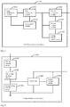
Fig. 1 is a schematic structural diagram of a two-stage switch power supply according to an embodiment of the present invention; -
Fig. 2 is a schematic structural diagram of a voltage limiting switch module in a two-stage switch power supply according to an embodiment of the present invention; -
Fig. 3 is a schematic structural diagram of a first control module in a two-stage switch power supply according to an embodiment of the present invention; -
Fig. 4 is a circuit diagram of a two-stage switch power supply according to another embodiment of the present invention. - The present invention will be further described in detail below with reference to the attached drawings and embodiments in order to make the objects, technical solutions, and advantages of the present invention clearer. It is to be understood that the specific embodiments described herein are merely illustrative of the present invention and are not intended to limit the present invention.
- The following specific embodiments will be described to explain the technical solutions of the present invention.
- An embodiment of the present invention provides a two-stage
switch power supply 10. As shown inFig. 1 , the two-stageswitch power supply 10 includes aninput rectification module 101, afirst control module 102, afirst conversion module 103, asecond control module 106, asecond conversion module 104, and a voltagelimiting switch module 105;
an output end of theinput rectification module 101 is connected to a voltage input end of thefirst control module 102 and a voltage input end of thefirst conversion module 103, a signal output end of thefirst control module 102 is connected to a control end of thefirst conversion module 103, a voltage output end of thefirst conversion module 103 is connected to a voltage input end of thesecond conversion module 104, a first voltage input end of the voltagelimiting switch module 105, and a voltage input end of thesecond control module 106, a second voltage input end of the voltagelimiting switch module 105 is connected to a control end of thesecond control module 106, an output end of thesecond control module 106 is connected to a second voltage input end and a third voltage input end of thesecond conversion module 104;
theinput rectification module 101 performs rectification and filtering on an input voltage and then outputs a rectification filtering voltage signal to thefirst control module 102 and thefirst conversion module 103;
thefirst control module 102 starts according to the rectification filtering voltage signal, and controls thefirst conversion module 103 to perform voltage conversion on the rectification filtering voltage signal so as to acquire a power supply voltage and a bus voltage;
thefirst conversion module 103 outputs the power supply voltage to thefirst control module 102 and outputs the bus voltage to thesecond conversion module 104, the voltagelimiting switch module 105, and thesecond control module 106;
the voltagelimiting switch module 105 controls, when the bus voltage reaches a preset voltage, thesecond control module 106 to output a voltage signal to thesecond conversion module 104 so as to control thesecond conversion module 104 to convert the bus voltage and then output the voltage to a load. - In the present embodiment of the present invention, the
input rectification module 101 is configured to perform rectification and filtering on an input alternating current and then to supply power to thefirst control module 102 and thefirst conversion module 103. Thefirst control module 102 starts and controls thefirst conversion module 103 to work. Thefirst conversion module 103 outputs a voltage to supply power to thefirst control module 102 on the one hand, and to supply power to thesecond conversion module 104, the voltagelimiting switch module 105, and thesecond control module 106 on the other hand. In this case, after receiving the voltage output by thefirst conversion module 103, the voltagelimiting switch module 105 does not immediately control thesecond control module 106 to work until the voltage output by thefirst conversion module 103 reaches a preset voltage, and then thesecond control module 106 controls thesecond conversion module 104 to start working. Although the output end of thesecond conversion module 104 is connected to the load, since the output voltage of thefirst conversion module 103 is high, it does not cause too much power supplied to the load to make thefirst control module 102 be in an intermittent working state. Here, the voltage limitingswitch module 105 may be a delay module consisting of discrete components, or may be a delay voltage limiting chip. - Further, the voltage limiting
switch module 105 is in an on state connected to the ground when the bus voltage has not reached the preset voltage, and the control end of thesecond control module 106 is connected to the ground;
the voltage limitingswitch module 105 is disconnected from the ground when the bus voltage reaches the preset voltage, and thesecond control module 106 charges the voltagelimiting switch module 105 through its control end so as to make thesecond control module 106 reach a working state. - Specifically, the
second control module 106 may be a control chip. The working principle of the control chip is that a voltage is output to the voltage limitingswitch module 105 through a soft start function pin, and when the voltage value stored on the voltage limitingswitch module 105 reaches a preset value, the control chip is made to work. In order to prevent the control chip from working when the output voltage of thefirst conversion module 103 is small, it is in an on state connected to the ground when the bus voltage has not reached the preset voltage, and the soft start function pin of the control chip is connected to the ground. At this time, the voltage value stored on the voltage limitingswitch module 105 is 0, and the control chip does not work. When the bus voltage reaches the preset voltage, it is disconnected from the ground, and the control chip charges the voltage limitingswitch module 105 through the soft start function pin so as to make thesecond control module 106 reach a working state. - As an embodiment, as shown in
Fig. 2 , the voltagelimiting switch module 105 includes a voltage limiting device 501, a firstvoltage dividing device 1502, a secondvoltage dividing device 1503, a switch tube 1504, and anenergy storage device 1505, wherein a first end of thevoltage limiting device 1501 is the voltage input end of the voltagelimiting switch module 105, a second end of thevoltage limiting device 1501 is connected to a first end of the firstvoltage dividing device 1502, a second end of the firstvoltage dividing device 1502 is connected to a control end of the switch tube 1504 and a first end of the secondvoltage dividing device 1503, an input end of the switch tube 1504 is connected to the control end of thesecond control module 106 and a first end of theenergy storage device 1505, an output end of the switch tube 1504, a second end of the secondvoltage dividing device 1503, and a second end of theenergy storage device 1505 are connected to the ground together;
thevoltage limiting device 1501 is in an off state when the bus voltage has not reached the preset voltage, and the switch tube 1504 is in an on state to connect the control end of thesecond control module 106 to the ground;
the voltage limiting device 1504 is in an on state when the bus voltage reaches the preset voltage, and the switch tube 1504 is in an off state so that thesecond control module 106 charges theenergy storage device 1505 through its control end so as to make thesecond control module 106 reach a working state. - Here, the voltage limiting device 1504 may be a voltage stabilizing tube, and a cathode and an anode of the voltage stabilizing tube are the first end and the second end of the voltage limiting device. The voltage limiting device 1504 may also be a chip with a voltage limiting function, and it is not limited herein.
- Here, as an embodiment, the switch tube 1504 is a PNP type triode, and a collector, an emitter, and a base of the PNP type triode are respectively the output end, the input end, and the control end of the switch tube.
- Here, as another embodiment, the switch tube 1504 is a P type MOS transistor, and a drain, a source, and a gate of the P type MOS transistor are respectively the output end, the input end, and the control end of the switch tube.
- Further, when the input voltage is powered off, the
first conversion module 103 stops working, thevoltage limiting device 1501 is in an off state, and the switch tube 1504 is in an on state to discharge the energy storage device to the ground. A rapid reset of the soft start function pin of the control chip is achieved by discharging the energy storage device to the ground, so that the soft start function pin has a soft start function in the next start process. - For the
first control module 102, as an embodiment, as shown inFig. 3 , thefirst control module 102 includes apower supply module 1201 and afirst control chip 1202, a voltage input end of thepower supply module 1201 is a voltage input end of thefirst control module 102, a voltage output end of thepower supply module 1201 is connected to the voltage input end of thefirst control chip 1202, and a voltage output end of thefirst control chip 1202 is a voltage output end of thefirst control module 102;
thepower supply module 1201 starts thefirst control chip 1202 according to the rectification filtering voltage signal;
thefirst control chip 1202 controls thefirst conversion module 103 to perform voltage conversion on the rectification filtering voltage signal so as to supply power to the power supply module;
thepower supply module 1201 outputs a power supply voltage to thefirst control chip 1202. - Specifically, after the
power supply module 1201 is started according to the output voltage of theinput rectification module 101, thefirst control module 102 is continuously powered according to the voltage output by thefirst conversion module 103, and a power supply can be achieved between thefirst conversion module 103 and the power supply module through an energy conversion device. - The embodiment of the present invention will be described in detail below through a specific circuit structure. As shown in
Fig. 4 :
For thefirst conversion module 103, specifically, thefirst conversion module 103 includes a resistor R1, a resistor R2, a resistor R5, a resistor R11, a resistor R69, a capacitor C4, a capacitor C63, a diode D2, a diode D61, a field effect transistor M1, and a transformer;
a first end of the resistor R1 is connected to a first end of the resistor C4 and a different terminal of a primary winding L1 of the transformer and constitutes the voltage input end of the first conversion module 103, a second end of the resistor R1 is connected to a first end of the resistor R2, a second end of the resistor R2 is connected to a second end of the capacitor C4 and a cathode of the diode D2, an anode of the diode D2 is connected to a dotted terminal of the primary winding L1 of the transformer and a drain of the field effect transistor M1, a gate of the field effect transistor M1 is connected to a first end of the resistor R5, a second end of the resistor R5 is the control end of the first conversion module 103, a source of the field effect transistor M1 is connected to a first end of the resistor R11, a second end of the resistor R11 is connected to the ground, a dotted terminal of a first secondary winding L2 of the transformer is connected to an anode of the diode D61, a cathode of the diode D61 is connected to a first end of the capacitor C63 and a first end of the resistor R69, a different terminal of the first secondary winding L2 of the transformer, a second end of the capacitor C63, and a second end of the resistor R69 are connected to the ground together. - For the power supply module, specifically, the power supply module includes a resistor R21, a resistor R22, a resistor R23, a resistor R24, a resistor R25, a capacitor C21, a capacitor C22, a triode Q21, a voltage stabilizing tube ZD22 and a diode D22;
a first end of the resistor R21 is the voltage input end of the power supply module, a second end of the resistor R21 is connected to a first end of the resistor R22, a second end of the resistor R22 is connected to a first end of the resistor R23, a second end of the resistor R23 is connected to an emitter of the triode Q21 and a first end of the capacitor C21 and constitutes the voltage output end of the power supply module, a base of the triode Q21 is connected to a first end of the resistor R24 and a cathode of the voltage stabilizing tube ZD22, a second end of the resistor R24 is connected to a collector of the triode Q21, a first end of the capacitor C22, and a cathode of the diode D22, an anode of the diode D22 is connected to a first end of the resistor R25, a second end of the resistor R25 is connected to a dotted terminal of a second secondary winding L3 of the transformer, a different terminal of the second secondary winding L3 of the transformer, a second end of the capacitor C22, an anode of the voltage stabilizing tube ZD22, and a second end of the capacitor C21 are connected to the ground together. - For a voltage limiting delay module, specifically, the voltage limiting delay module includes a voltage stabilizing tube ZD71, a resistor R71, a resistor R72, a triode Q71, and a capacitor C70, a cathode of the voltage stabilizing tube ZD71 is a voltage input end of the voltage limiting delay module, an anode of the voltage stabilizing tube ZD71 is connected to a first end of the resistor R71, a second end of the resistor R71 is connected to a first end of the resistor R72 and a base of the triode Q71, a collector of the triode Q71 is connected to a first end of the capacitor C70, a second end of the resistor R72, an emitter of the triode Q71, and a second end of the capacitor C70 are connected to the ground.
- For the
second conversion module 104, specifically, thesecond conversion module 104 includes a resistor R65, a diode D62, a power inductor L61, and a capacitor C62, a first end of the resistor R65 is connected to a cathode of the diode D62 and constitutes a first voltage input end of the second conversion module, a second end of the resistor R65 is connected to a first end of the capacitor C62 and constitutes a first voltage output end of thesecond conversion module 104, an anode of the diode D62 is connected to a first end of the power inductor L61, a second end of the power inductor L61 is connected to a second end of the capacitor C62 and constitutes a second voltage output end of thesecond conversion module 104. - After the input voltage is rectified and filtered by the
input rectification module 101, a voltage drop is formed on the capacitor C2, and this voltage charges the capacitor C21 via the resistor R21, the resistor R22, and the resistor R23. When the voltage of the capacitor C21 rises to a turn-on voltage of a first control chip U10, a first-stage control circuit starts to work, an OUT pin of the first control chip U10 outputs a PWM type to modulate a first-stage conversion module, a control switch tube M1 performs a high-frequency switching operation, the first primary winding L1 of the transformer L20 obtains an induced voltage, the first secondary winding L2 outputs a PWM voltage, which is rectified by the diode D61 and filtered by the capacitor C63 to obtain a bus voltage Vbus, and the output of the second secondary winding L3 is rectified by the diode D22 and filtered by the capacitor C22 to obtain a direct current voltage to be supplied to the first control chip. - When the bus voltage Vbus has not risen to a value greater than a voltage stabilizing value of the voltage stabilizing tube ZD71, the voltage stabilizing tube ZD71 is in an off state. At this time, the dividing voltage passing through the resistor R71 and the resistor R72 makes the base voltage of the triode Q71 close to 0V, the triode Q71 is forward-biased on, shorting the soft start PWM pin to ground and preventing its voltage from rising, and the second-stage conversion module has no output.
- When the bus voltage Vbus rises to a value greater than the voltage stabilizing value of the voltage stabilizing tube ZD71, the voltage stabilizing tube ZD71 is reversely broken down. At this time, the dividing voltage of the resistor R71 and the resistor R72 causes the base voltage of the triode Q71 to rise. When this voltage is greater than a voltage obtained by subtracting a triode E-B saturation voltage (about 0.7V in the case of a triode) from the voltage of the capacitor C70, the triode Q71 starts to be reverse-biased off, a second control chip IC starts to charge the capacitor C70 via the PWM pin (the soft start function pin). As the voltage of the capacitor C70 increases, the second-stage conversion module starts to work and the output voltage/current also increases. The second-stage conversion module starts to work and achieves a soft start when the output voltage Vbus of the first-stage conversion module reaches a high value. Therefore, after the second-stage conversion module outputs to bring a load, the decrease in the bus voltage Vbus does not become too low to cause the voltage of a VCC winding, i.e., the second secondary winding L3, to be too low, which will cause an intermittent working state of the first control chip IC U10. As a result, an overall smooth start is achieved.
- In another corresponding case, when the input voltage of the
input rectification module 101 is powered off, thefirst conversion module 103 quickly stops working and stops supplying energy to thesecond conversion module 104. Therefore, the bus voltage Vbus also rapidly decreases. As a result, the voltage stabilizing tube ZD71 is off, the triode Q71 is forward-biased on, and the charge stored on the capacitor C70 is rapidly discharged through the triode Q71, achieving a rapid reset of the soft start PWM pin so that a soft start function is provided in the next start process. - In the embodiment of the present invention, a delay control is performed on the start of a second-stage control module during the starting process, and a rapid start with high efficiency and low loss is achieved; meanwhile, a rapid reset is performed on the soft start of a second-stage control circuit when the input voltage is powered off, so that the soft start function is still provided when the input is being rapidly switched on and off. The present technical solution is achieved with a simple structure and a low overall cost.
- The above content is a further detailed description of the present invention in combination with specific preferred embodiments, and specific embodiments of the present invention are not limited to the description. For those of ordinary skill in the art, equivalent substitutions or obvious variations made without departing from the inventive concept of the present invention and having the same performance or use shall be considered to be within the patent protection scope of the present invention as defined by the submitted claims.
Claims (10)
- A two-stage switch power supply which is characterized in that the two-stage switch power supply comprises an input rectification module, a first control module, a first conversion module, a second control module, a second conversion module, and a voltage limiting switch module;
an output end of the input rectification module is connected to a voltage input end of the first control module and a voltage input end of the first conversion module, a signal output end of the first control module is connected to a control end of the first conversion module, a voltage output end of the first conversion module is connected to a voltage input end of the second conversion module, a first voltage input end of the voltage limiting switch module, and a voltage input end of the second control module, a second voltage input end of the voltage limiting switch module is connected to a control end of the second control module, an output end of the second control module is connected to a second voltage input end and a third voltage input end of the second conversion module;
the input rectification module performs rectification and filtering on an input voltage and then outputs a rectification filtering voltage signal to the first control module and the first conversion module;
the first control module starts according to the rectification filtering voltage signal, and controls the first conversion module to perform voltage conversion on the rectification filtering voltage signal so as to acquire a power supply voltage and a bus voltage;
the first conversion module outputs the power supply voltage to the first control module and outputs the bus voltage to the second conversion module, the voltage limiting switch module, and the second control module;
the voltage limiting switch module controls, when the bus voltage reaches a preset voltage, the second control module to output a voltage signal to the second conversion module so as to control the second conversion module to convert the bus voltage and then output the voltage to a load. - The two-stage switch power supply according to claim 1, characterized in that the voltage limiting switch module is in an on state connected to the ground when the bus voltage has not reached the preset voltage, and the control end of the second control module is connected to the ground;
for the voltage limiting switch module when the bus voltage reaches the preset voltage, the second control module charges the voltage limiting switch module through its control end so as to make the second control module reach a working state. - The two-stage switch power supply according to claim 2, characterized in that the voltage limiting switch module includes a voltage limiting device, a first voltage dividing device, a second voltage dividing device, a switch tube, and an energy storage device, wherein a first end of the voltage limiting device is the voltage input end of the voltage limiting switch module, a second end of the voltage limiting device is connected to a first end of the first voltage dividing device, a second end of the first voltage dividing device is connected to a control end of the switch tube and a first end of the second voltage dividing device, an input end of the switch tube is connected to the control end of the second control module and a first end of the energy storage device, an output end of the switch tube, a second end of the second voltage dividing device, and a second end of the energy storage device are connected to the ground together;
the voltage limiting device is in an off state when the bus voltage has not reached the preset voltage, and the switch tube is in an on state to connect the control end of the second control module to the ground;
the voltage limiting device is in an on state when the bus voltage reaches the preset voltage, and the switch tube is in an off state so that the second control module charges the energy storage device through its control end so as to make the second control module reach a working state. - The two-stage switch power supply according to claim 3, characterized in that when the first conversion module stops working, the voltage limiting device is in an off state, and the switch tube is in an on state to discharge the energy storage device to the ground.
- The two-stage switch power supply according to claim 3, characterized in that the voltage limiting device is a voltage stabilizing tube, and a cathode and an anode of the voltage stabilizing tube are the first end and the second end of the voltage limiting device.
- The two-stage switch power supply according to claim 3, characterized in that the switch tube is a PNP type triode, and a collector, an emitter, and a base of the PNP type triode are respectively the output end, the input end, and the control end of the switch tube.
- The two-stage switch power supply according to claim 3, characterized in that the switch tube is a P type MOS transistor, and a drain, a source, and a gate of the P type MOS transistor are respectively the output end, the input end, and the control end of the switch tube.
- The two-stage switch power supply according to claim 1, characterized in that the first control circuit includes a power supply module and a first control chip, a voltage input end of the power supply module is a voltage input end of the first control circuit, a voltage output end of the power supply module is connected to the voltage input end of the first control chip, and a voltage output end of the first control chip is a voltage output end of the first control circuit;
the power supply module starts the first control chip according to the rectification filtering voltage signal;
the first control chip controls the first conversion module to perform voltage conversion on the rectification filtering voltage signal;
the power supply module outputs a power supply voltage to the first control chip. - The two-stage switch power supply according to claim 8, characterized in that the first conversion module includes a resistor R1, a resistor R2, a resistor R5, a resistor R11, a resistor R69, a capacitor C4, a capacitor C63, a diode D2, a diode D61, a field effect transistor M1, and a transformer;
a first end of the resistor R1 is connected to a first end of the resistor C4 and a different terminal of a primary winding L1 of the transformer and constitutes the voltage input end of the first conversion module, a second end of the resistor R1 is connected to a first end of the resistor R2, a second end of the resistor R2 is connected to a second end of the capacitor C4 and a cathode of the diode D2, an anode of the diode D2 is connected to a dotted terminal of the primary winding L1 of the transformer and a drain of the field effect transistor M1, a gate of the field effect transistor M1 is connected to a first end of the resistor R5, a second end of the resistor R5 is the control end of the first conversion module, a source of the field effect transistor M1 is connected to a first end of the resistor R11, a second end of the resistor R11 is connected to the ground, a dotted terminal of a first secondary winding L2 of the transformer is connected to an anode of the diode D61, a cathode of the diode D61 is connected to a first end of the capacitor C63 and a first end of the resistor R69, a different terminal of the first secondary winding L2 of the transformer, a second end of the capacitor C63, and a second end of the resistor R69 are connected to the ground together. - The two-stage switch power supply according to claim 9, characterized in that the power supply module includes a resistor R21, a resistor R22, a resistor R23, a resistor R24, a resistor R25, a capacitor C21, a capacitor C22, a triode Q21, a voltage stabilizing tube ZD22 and a diode D22;
a first end of the resistor R21 is the voltage input end of the power supply module, a second end of the resistor R21 is connected to a first end of the resistor R22, a second end of the resistor R22 is connected to a first end of the resistor R23, a second end of the resistor R23 is connected to an emitter of the triode Q21 and a first end of the capacitor C21 and constitutes the voltage output end of the power supply module, a base of the triode Q21 is connected to a first end of the resistor R24 and a cathode of the voltage stabilizing tube ZD22, a second end of the resistor R24 is connected to a collector of the triode Q21, a first end of the capacitor C22, and a cathode of the diode D22, an anode of the diode D22 is connected to a first end of the resistor R25, a second end of the resistor R25 is connected to a dotted terminal of a second secondary winding L3 of the transformer, a different terminal of the second secondary winding L3 of the transformer, a second end of the capacitor C22, an anode of the voltage stabilizing tube ZD22, and a second end of the capacitor C21 are connected to the ground together.
Applications Claiming Priority (2)
| Application Number | Priority Date | Filing Date | Title |
|---|---|---|---|
| CN201710169436.7A CN108631565B (en) | 2017-03-21 | 2017-03-21 | Two-stage switch power supply |
| PCT/CN2018/079740 WO2018171613A1 (en) | 2017-03-21 | 2018-03-21 | Two-stage switch power supply |
Publications (3)
| Publication Number | Publication Date |
|---|---|
| EP3584917A1 true EP3584917A1 (en) | 2019-12-25 |
| EP3584917A4 EP3584917A4 (en) | 2020-05-20 |
| EP3584917B1 EP3584917B1 (en) | 2022-01-26 |
Family
ID=63584164
Family Applications (1)
| Application Number | Title | Priority Date | Filing Date |
|---|---|---|---|
| EP18771684.0A Active EP3584917B1 (en) | 2017-03-21 | 2018-03-21 | Two-stage switch power supply |
Country Status (3)
| Country | Link |
|---|---|
| EP (1) | EP3584917B1 (en) |
| CN (1) | CN108631565B (en) |
| WO (1) | WO2018171613A1 (en) |
Families Citing this family (4)
| Publication number | Priority date | Publication date | Assignee | Title |
|---|---|---|---|---|
| CN109941124A (en) * | 2019-02-14 | 2019-06-28 | 深圳市永联科技股份有限公司 | Charging pile and its charging module and charging and voltage stabilizing control method |
| CN112631357B (en) * | 2020-12-22 | 2022-10-21 | 博科能源系统(深圳)有限公司 | DC voltage-stabilized power supply circuit |
| CN116545245A (en) * | 2022-01-26 | 2023-08-04 | 维谛公司 | A Soft Start Circuit and Flyback Converter |
| CN115102561A (en) * | 2022-07-04 | 2022-09-23 | 禹创半导体(深圳)有限公司 | Device for reducing differential transmission electromagnetic interference by regulating and controlling conversion efficiency |
Family Cites Families (16)
| Publication number | Priority date | Publication date | Assignee | Title |
|---|---|---|---|---|
| JP3236587B2 (en) * | 1999-09-30 | 2001-12-10 | 長野日本無線株式会社 | Switching power supply |
| JP3553042B2 (en) * | 2001-12-03 | 2004-08-11 | サンケン電気株式会社 | Switching power supply device and driving method thereof |
| KR100597379B1 (en) * | 2002-02-08 | 2006-07-10 | 산켄덴키 가부시키가이샤 | Starting method of power supply, starting circuit of power supply and power supply |
| CN2653774Y (en) * | 2003-10-22 | 2004-11-03 | 广州珠江电信设备制造有限公司 | High frequency switch power commutating module for communication equipment |
| JP4793226B2 (en) * | 2006-11-09 | 2011-10-12 | 株式会社デンソー | Switching boost power supply circuit |
| CN101378230B (en) * | 2007-08-31 | 2011-06-15 | 群康科技(深圳)有限公司 | Switch power supply circuit |
| JP2012152066A (en) * | 2011-01-20 | 2012-08-09 | Olympus Corp | Power supply device |
| CN202268808U (en) * | 2011-09-15 | 2012-06-06 | 北京国网普瑞特高压输电技术有限公司 | Current control single channel output fly-back converter |
| CN103227560B (en) * | 2013-03-28 | 2015-08-19 | 华为技术有限公司 | Start the method and apparatus of inverter |
| CN103929055A (en) * | 2014-04-30 | 2014-07-16 | 矽力杰半导体技术(杭州)有限公司 | Power supply circuit and switching power supply |
| TWI548186B (en) * | 2014-08-15 | 2016-09-01 | Richtek Technology Corp | Quick Start Circuit and Method of Chi - back Power Supply |
| JP6266171B2 (en) * | 2014-09-12 | 2018-01-24 | フィリップス ライティング ホールディング ビー ヴィ | Power circuit |
| CN104377950B (en) * | 2014-11-05 | 2017-02-15 | 深圳市汇川技术股份有限公司 | Starting circuit of power supply control chip |
| CN104734516B (en) * | 2015-02-11 | 2017-12-15 | 深圳市航嘉驰源电气股份有限公司 | Switching power circuit and computer power supply |
| CN204424869U (en) * | 2015-02-12 | 2015-06-24 | 东莞理工学院 | A Hiccup Protection Circuit and a Photovoltaic Power Generation System Using the Circuit |
| CN205160363U (en) * | 2015-11-27 | 2016-04-13 | 英飞特电子(杭州)股份有限公司 | Auxiliary power supply circuit and switching power supply |
-
2017
- 2017-03-21 CN CN201710169436.7A patent/CN108631565B/en active Active
-
2018
- 2018-03-21 EP EP18771684.0A patent/EP3584917B1/en active Active
- 2018-03-21 WO PCT/CN2018/079740 patent/WO2018171613A1/en not_active Ceased
Also Published As
| Publication number | Publication date |
|---|---|
| CN108631565B (en) | 2020-04-28 |
| WO2018171613A1 (en) | 2018-09-27 |
| CN108631565A (en) | 2018-10-09 |
| EP3584917B1 (en) | 2022-01-26 |
| EP3584917A4 (en) | 2020-05-20 |
Similar Documents
| Publication | Publication Date | Title |
|---|---|---|
| US8669748B2 (en) | Device for synchronous DC-DC conversion and synchronous DC-DC converter | |
| US9182629B2 (en) | LED backlight source drive circuit, LED backlight source and liquid crystal display device | |
| US20100013548A1 (en) | Power efficient charge pump with controlled peak currents | |
| WO2022027264A1 (en) | Drive circuit for channel switch, charging control method and charger | |
| US10236879B2 (en) | Thyristor driving apparatus | |
| US9231415B2 (en) | Stored electric power discharging circuit for inverter | |
| US10622879B2 (en) | Control module with active snubber and related flyback power converting device | |
| US9590503B2 (en) | Switching converter and associated discharge method | |
| EP3584917B1 (en) | Two-stage switch power supply | |
| CN105162313B (en) | A kind of inverse-excitation type switch power-supply | |
| US20180069428A1 (en) | Charging-discharging module of energy storage unit and charging-discharging method thereof | |
| CN110994774A (en) | Power supply switching circuit | |
| JP2015192597A (en) | Switch circuit for controlling power supply to load | |
| US8619439B2 (en) | Flyback boost circuit with current supplied to secondary side of transformer circuit prior to boost operation and strobe device using the same | |
| CN110855170A (en) | Photovoltaic inverter and capacitor discharge circuit | |
| CN106655749B (en) | A power control circuit and a switching power supply using the same | |
| US20220124888A1 (en) | Buck topological circuit for power supply | |
| US8213196B2 (en) | Power supply circuit with protecting circuit having switch element for protecting pulse width modulation circuit | |
| TWI538333B (en) | Soft-start switch circuit and electronic apparatus | |
| CN113037070B (en) | Fast starting circuit of switching power supply | |
| US20160135260A1 (en) | Switching circuit for light-emitting diode | |
| CN107332435B (en) | Power supply circuit of pulse width modulation chip and switching power supply | |
| CN111048055A (en) | Display and display standby power consumption control method | |
| US11128292B2 (en) | Soft-start control circuit | |
| US20130272034A1 (en) | Method of forming a low power dissipation regulator and structure therefor |
Legal Events
| Date | Code | Title | Description |
|---|---|---|---|
| STAA | Information on the status of an ep patent application or granted ep patent |
Free format text: STATUS: THE INTERNATIONAL PUBLICATION HAS BEEN MADE |
|
| PUAI | Public reference made under article 153(3) epc to a published international application that has entered the european phase |
Free format text: ORIGINAL CODE: 0009012 |
|
| STAA | Information on the status of an ep patent application or granted ep patent |
Free format text: STATUS: REQUEST FOR EXAMINATION WAS MADE |
|
| 17P | Request for examination filed |
Effective date: 20190920 |
|
| AK | Designated contracting states |
Kind code of ref document: A1 Designated state(s): AL AT BE BG CH CY CZ DE DK EE ES FI FR GB GR HR HU IE IS IT LI LT LU LV MC MK MT NL NO PL PT RO RS SE SI SK SM TR |
|
| AX | Request for extension of the european patent |
Extension state: BA ME |
|
| A4 | Supplementary search report drawn up and despatched |
Effective date: 20200421 |
|
| RIC1 | Information provided on ipc code assigned before grant |
Ipc: H02M 1/36 20070101AFI20200415BHEP Ipc: H02M 1/00 20060101ALI20200415BHEP Ipc: H02M 1/32 20070101ALI20200415BHEP |
|
| DAV | Request for validation of the european patent (deleted) | ||
| DAX | Request for extension of the european patent (deleted) | ||
| STAA | Information on the status of an ep patent application or granted ep patent |
Free format text: STATUS: EXAMINATION IS IN PROGRESS |
|
| 17Q | First examination report despatched |
Effective date: 20201221 |
|
| GRAP | Despatch of communication of intention to grant a patent |
Free format text: ORIGINAL CODE: EPIDOSNIGR1 |
|
| STAA | Information on the status of an ep patent application or granted ep patent |
Free format text: STATUS: GRANT OF PATENT IS INTENDED |
|
| INTG | Intention to grant announced |
Effective date: 20211103 |
|
| GRAS | Grant fee paid |
Free format text: ORIGINAL CODE: EPIDOSNIGR3 |
|
| GRAA | (expected) grant |
Free format text: ORIGINAL CODE: 0009210 |
|
| STAA | Information on the status of an ep patent application or granted ep patent |
Free format text: STATUS: THE PATENT HAS BEEN GRANTED |
|
| AK | Designated contracting states |
Kind code of ref document: B1 Designated state(s): AL AT BE BG CH CY CZ DE DK EE ES FI FR GB GR HR HU IE IS IT LI LT LU LV MC MK MT NL NO PL PT RO RS SE SI SK SM TR |
|
| REG | Reference to a national code |
Ref country code: GB Ref legal event code: FG4D |
|
| REG | Reference to a national code |
Ref country code: CH Ref legal event code: EP |
|
| REG | Reference to a national code |
Ref country code: AT Ref legal event code: REF Ref document number: 1466050 Country of ref document: AT Kind code of ref document: T Effective date: 20220215 |
|
| REG | Reference to a national code |
Ref country code: IE Ref legal event code: FG4D |
|
| REG | Reference to a national code |
Ref country code: DE Ref legal event code: R096 Ref document number: 602018030125 Country of ref document: DE |
|
| REG | Reference to a national code |
Ref country code: LT Ref legal event code: MG9D |
|
| REG | Reference to a national code |
Ref country code: NL Ref legal event code: MP Effective date: 20220126 |
|
| PG25 | Lapsed in a contracting state [announced via postgrant information from national office to epo] |
Ref country code: NL Free format text: LAPSE BECAUSE OF FAILURE TO SUBMIT A TRANSLATION OF THE DESCRIPTION OR TO PAY THE FEE WITHIN THE PRESCRIBED TIME-LIMIT Effective date: 20220126 |
|
| PG25 | Lapsed in a contracting state [announced via postgrant information from national office to epo] |
Ref country code: SE Free format text: LAPSE BECAUSE OF FAILURE TO SUBMIT A TRANSLATION OF THE DESCRIPTION OR TO PAY THE FEE WITHIN THE PRESCRIBED TIME-LIMIT Effective date: 20220126 Ref country code: RS Free format text: LAPSE BECAUSE OF FAILURE TO SUBMIT A TRANSLATION OF THE DESCRIPTION OR TO PAY THE FEE WITHIN THE PRESCRIBED TIME-LIMIT Effective date: 20220126 Ref country code: PT Free format text: LAPSE BECAUSE OF FAILURE TO SUBMIT A TRANSLATION OF THE DESCRIPTION OR TO PAY THE FEE WITHIN THE PRESCRIBED TIME-LIMIT Effective date: 20220526 Ref country code: NO Free format text: LAPSE BECAUSE OF FAILURE TO SUBMIT A TRANSLATION OF THE DESCRIPTION OR TO PAY THE FEE WITHIN THE PRESCRIBED TIME-LIMIT Effective date: 20220426 Ref country code: LT Free format text: LAPSE BECAUSE OF FAILURE TO SUBMIT A TRANSLATION OF THE DESCRIPTION OR TO PAY THE FEE WITHIN THE PRESCRIBED TIME-LIMIT Effective date: 20220126 Ref country code: HR Free format text: LAPSE BECAUSE OF FAILURE TO SUBMIT A TRANSLATION OF THE DESCRIPTION OR TO PAY THE FEE WITHIN THE PRESCRIBED TIME-LIMIT Effective date: 20220126 Ref country code: ES Free format text: LAPSE BECAUSE OF FAILURE TO SUBMIT A TRANSLATION OF THE DESCRIPTION OR TO PAY THE FEE WITHIN THE PRESCRIBED TIME-LIMIT Effective date: 20220126 Ref country code: BG Free format text: LAPSE BECAUSE OF FAILURE TO SUBMIT A TRANSLATION OF THE DESCRIPTION OR TO PAY THE FEE WITHIN THE PRESCRIBED TIME-LIMIT Effective date: 20220426 |
|
| PG25 | Lapsed in a contracting state [announced via postgrant information from national office to epo] |
Ref country code: PL Free format text: LAPSE BECAUSE OF FAILURE TO SUBMIT A TRANSLATION OF THE DESCRIPTION OR TO PAY THE FEE WITHIN THE PRESCRIBED TIME-LIMIT Effective date: 20220126 Ref country code: LV Free format text: LAPSE BECAUSE OF FAILURE TO SUBMIT A TRANSLATION OF THE DESCRIPTION OR TO PAY THE FEE WITHIN THE PRESCRIBED TIME-LIMIT Effective date: 20220126 Ref country code: GR Free format text: LAPSE BECAUSE OF FAILURE TO SUBMIT A TRANSLATION OF THE DESCRIPTION OR TO PAY THE FEE WITHIN THE PRESCRIBED TIME-LIMIT Effective date: 20220427 Ref country code: FI Free format text: LAPSE BECAUSE OF FAILURE TO SUBMIT A TRANSLATION OF THE DESCRIPTION OR TO PAY THE FEE WITHIN THE PRESCRIBED TIME-LIMIT Effective date: 20220126 |
|
| PG25 | Lapsed in a contracting state [announced via postgrant information from national office to epo] |
Ref country code: IS Free format text: LAPSE BECAUSE OF FAILURE TO SUBMIT A TRANSLATION OF THE DESCRIPTION OR TO PAY THE FEE WITHIN THE PRESCRIBED TIME-LIMIT Effective date: 20220526 |
|
| REG | Reference to a national code |
Ref country code: DE Ref legal event code: R097 Ref document number: 602018030125 Country of ref document: DE |
|
| PG25 | Lapsed in a contracting state [announced via postgrant information from national office to epo] |
Ref country code: SM Free format text: LAPSE BECAUSE OF FAILURE TO SUBMIT A TRANSLATION OF THE DESCRIPTION OR TO PAY THE FEE WITHIN THE PRESCRIBED TIME-LIMIT Effective date: 20220126 Ref country code: SK Free format text: LAPSE BECAUSE OF FAILURE TO SUBMIT A TRANSLATION OF THE DESCRIPTION OR TO PAY THE FEE WITHIN THE PRESCRIBED TIME-LIMIT Effective date: 20220126 Ref country code: RO Free format text: LAPSE BECAUSE OF FAILURE TO SUBMIT A TRANSLATION OF THE DESCRIPTION OR TO PAY THE FEE WITHIN THE PRESCRIBED TIME-LIMIT Effective date: 20220126 Ref country code: MC Free format text: LAPSE BECAUSE OF FAILURE TO SUBMIT A TRANSLATION OF THE DESCRIPTION OR TO PAY THE FEE WITHIN THE PRESCRIBED TIME-LIMIT Effective date: 20220126 Ref country code: EE Free format text: LAPSE BECAUSE OF FAILURE TO SUBMIT A TRANSLATION OF THE DESCRIPTION OR TO PAY THE FEE WITHIN THE PRESCRIBED TIME-LIMIT Effective date: 20220126 Ref country code: DK Free format text: LAPSE BECAUSE OF FAILURE TO SUBMIT A TRANSLATION OF THE DESCRIPTION OR TO PAY THE FEE WITHIN THE PRESCRIBED TIME-LIMIT Effective date: 20220126 Ref country code: CZ Free format text: LAPSE BECAUSE OF FAILURE TO SUBMIT A TRANSLATION OF THE DESCRIPTION OR TO PAY THE FEE WITHIN THE PRESCRIBED TIME-LIMIT Effective date: 20220126 |
|
| REG | Reference to a national code |
Ref country code: CH Ref legal event code: PL |
|
| PG25 | Lapsed in a contracting state [announced via postgrant information from national office to epo] |
Ref country code: AL Free format text: LAPSE BECAUSE OF FAILURE TO SUBMIT A TRANSLATION OF THE DESCRIPTION OR TO PAY THE FEE WITHIN THE PRESCRIBED TIME-LIMIT Effective date: 20220126 |
|
| PLBE | No opposition filed within time limit |
Free format text: ORIGINAL CODE: 0009261 |
|
| STAA | Information on the status of an ep patent application or granted ep patent |
Free format text: STATUS: NO OPPOSITION FILED WITHIN TIME LIMIT |
|
| REG | Reference to a national code |
Ref country code: BE Ref legal event code: MM Effective date: 20220331 |
|
| 26N | No opposition filed |
Effective date: 20221027 |
|
| PG25 | Lapsed in a contracting state [announced via postgrant information from national office to epo] |
Ref country code: LU Free format text: LAPSE BECAUSE OF NON-PAYMENT OF DUE FEES Effective date: 20220321 Ref country code: LI Free format text: LAPSE BECAUSE OF NON-PAYMENT OF DUE FEES Effective date: 20220331 Ref country code: IE Free format text: LAPSE BECAUSE OF NON-PAYMENT OF DUE FEES Effective date: 20220321 Ref country code: CH Free format text: LAPSE BECAUSE OF NON-PAYMENT OF DUE FEES Effective date: 20220331 |
|
| PG25 | Lapsed in a contracting state [announced via postgrant information from national office to epo] |
Ref country code: SI Free format text: LAPSE BECAUSE OF FAILURE TO SUBMIT A TRANSLATION OF THE DESCRIPTION OR TO PAY THE FEE WITHIN THE PRESCRIBED TIME-LIMIT Effective date: 20220126 Ref country code: BE Free format text: LAPSE BECAUSE OF NON-PAYMENT OF DUE FEES Effective date: 20220331 |
|
| P01 | Opt-out of the competence of the unified patent court (upc) registered |
Effective date: 20230530 |
|
| PG25 | Lapsed in a contracting state [announced via postgrant information from national office to epo] |
Ref country code: IT Free format text: LAPSE BECAUSE OF FAILURE TO SUBMIT A TRANSLATION OF THE DESCRIPTION OR TO PAY THE FEE WITHIN THE PRESCRIBED TIME-LIMIT Effective date: 20220126 |
|
| PG25 | Lapsed in a contracting state [announced via postgrant information from national office to epo] |
Ref country code: MK Free format text: LAPSE BECAUSE OF FAILURE TO SUBMIT A TRANSLATION OF THE DESCRIPTION OR TO PAY THE FEE WITHIN THE PRESCRIBED TIME-LIMIT Effective date: 20220126 Ref country code: CY Free format text: LAPSE BECAUSE OF FAILURE TO SUBMIT A TRANSLATION OF THE DESCRIPTION OR TO PAY THE FEE WITHIN THE PRESCRIBED TIME-LIMIT Effective date: 20220126 |
|
| REG | Reference to a national code |
Ref country code: AT Ref legal event code: MM01 Ref document number: 1466050 Country of ref document: AT Kind code of ref document: T Effective date: 20230321 |
|
| PG25 | Lapsed in a contracting state [announced via postgrant information from national office to epo] |
Ref country code: HU Free format text: LAPSE BECAUSE OF FAILURE TO SUBMIT A TRANSLATION OF THE DESCRIPTION OR TO PAY THE FEE WITHIN THE PRESCRIBED TIME-LIMIT; INVALID AB INITIO Effective date: 20180321 |
|
| PG25 | Lapsed in a contracting state [announced via postgrant information from national office to epo] |
Ref country code: AT Free format text: LAPSE BECAUSE OF NON-PAYMENT OF DUE FEES Effective date: 20230321 |
|
| PG25 | Lapsed in a contracting state [announced via postgrant information from national office to epo] |
Ref country code: AT Free format text: LAPSE BECAUSE OF NON-PAYMENT OF DUE FEES Effective date: 20230321 |
|
| PG25 | Lapsed in a contracting state [announced via postgrant information from national office to epo] |
Ref country code: MT Free format text: LAPSE BECAUSE OF FAILURE TO SUBMIT A TRANSLATION OF THE DESCRIPTION OR TO PAY THE FEE WITHIN THE PRESCRIBED TIME-LIMIT Effective date: 20220126 |
|
| REG | Reference to a national code |
Ref country code: DE Ref legal event code: R084 Ref document number: 602018030125 Country of ref document: DE |
|
| PGFP | Annual fee paid to national office [announced via postgrant information from national office to epo] |
Ref country code: FR Payment date: 20250324 Year of fee payment: 8 |
|
| PGFP | Annual fee paid to national office [announced via postgrant information from national office to epo] |
Ref country code: GB Payment date: 20250326 Year of fee payment: 8 |
|
| REG | Reference to a national code |
Ref country code: AT Ref legal event code: UEP Ref document number: 1466050 Country of ref document: AT Kind code of ref document: T Effective date: 20220126 |
|
| PG25 | Lapsed in a contracting state [announced via postgrant information from national office to epo] |
Ref country code: TR Free format text: LAPSE BECAUSE OF FAILURE TO SUBMIT A TRANSLATION OF THE DESCRIPTION OR TO PAY THE FEE WITHIN THE PRESCRIBED TIME-LIMIT Effective date: 20220126 |
|
| PGFP | Annual fee paid to national office [announced via postgrant information from national office to epo] |
Ref country code: DE Payment date: 20260320 Year of fee payment: 9 |
|
| PGFP | Annual fee paid to national office [announced via postgrant information from national office to epo] |
Ref country code: AT Payment date: 20260410 Year of fee payment: 5 |