EP3583980A1 - Feedthroughs - Google Patents
Feedthroughs Download PDFInfo
- Publication number
- EP3583980A1 EP3583980A1 EP18178542.9A EP18178542A EP3583980A1 EP 3583980 A1 EP3583980 A1 EP 3583980A1 EP 18178542 A EP18178542 A EP 18178542A EP 3583980 A1 EP3583980 A1 EP 3583980A1
- Authority
- EP
- European Patent Office
- Prior art keywords
- conductors
- electrical conductors
- ceramic
- feedthrough
- conductor
- Prior art date
- Legal status (The legal status is an assumption and is not a legal conclusion. Google has not performed a legal analysis and makes no representation as to the accuracy of the status listed.)
- Withdrawn
Links
- 239000004020 conductor Substances 0.000 claims abstract description 500
- 239000000919 ceramic Substances 0.000 claims abstract description 212
- 238000000034 method Methods 0.000 claims description 118
- 239000012530 fluid Substances 0.000 claims description 23
- 239000011159 matrix material Substances 0.000 claims description 22
- 239000012700 ceramic precursor Substances 0.000 claims description 20
- 238000004519 manufacturing process Methods 0.000 claims description 16
- 238000010344 co-firing Methods 0.000 claims description 7
- 238000003466 welding Methods 0.000 claims description 3
- BASFCYQUMIYNBI-UHFFFAOYSA-N platinum Chemical compound [Pt] BASFCYQUMIYNBI-UHFFFAOYSA-N 0.000 description 60
- 230000008569 process Effects 0.000 description 42
- 230000037361 pathway Effects 0.000 description 29
- 229910052697 platinum Inorganic materials 0.000 description 26
- 229910052751 metal Inorganic materials 0.000 description 24
- 239000002184 metal Substances 0.000 description 24
- 239000010410 layer Substances 0.000 description 20
- 229910045601 alloy Inorganic materials 0.000 description 16
- 239000000956 alloy Substances 0.000 description 16
- 238000005245 sintering Methods 0.000 description 16
- PXHVJJICTQNCMI-UHFFFAOYSA-N Nickel Chemical compound [Ni] PXHVJJICTQNCMI-UHFFFAOYSA-N 0.000 description 15
- PNEYBMLMFCGWSK-UHFFFAOYSA-N Alumina Chemical compound [O-2].[O-2].[O-2].[Al+3].[Al+3] PNEYBMLMFCGWSK-UHFFFAOYSA-N 0.000 description 14
- PCHJSUWPFVWCPO-UHFFFAOYSA-N gold Chemical compound [Au] PCHJSUWPFVWCPO-UHFFFAOYSA-N 0.000 description 12
- 229910052737 gold Inorganic materials 0.000 description 12
- 239000010931 gold Substances 0.000 description 12
- 238000005266 casting Methods 0.000 description 11
- 239000007787 solid Substances 0.000 description 11
- MCMNRKCIXSYSNV-UHFFFAOYSA-N Zirconium dioxide Chemical compound O=[Zr]=O MCMNRKCIXSYSNV-UHFFFAOYSA-N 0.000 description 10
- 238000013461 design Methods 0.000 description 10
- 239000000463 material Substances 0.000 description 10
- 229910052759 nickel Inorganic materials 0.000 description 10
- 239000011888 foil Substances 0.000 description 9
- 239000012212 insulator Substances 0.000 description 9
- 238000001878 scanning electron micrograph Methods 0.000 description 9
- 238000012360 testing method Methods 0.000 description 9
- 229910052741 iridium Inorganic materials 0.000 description 8
- XEEYBQQBJWHFJM-UHFFFAOYSA-N iron Substances [Fe] XEEYBQQBJWHFJM-UHFFFAOYSA-N 0.000 description 8
- 238000012545 processing Methods 0.000 description 8
- 229910001030 Iron–nickel alloy Inorganic materials 0.000 description 7
- 238000000227 grinding Methods 0.000 description 7
- 238000000926 separation method Methods 0.000 description 7
- 229910052721 tungsten Inorganic materials 0.000 description 7
- 230000001419 dependent effect Effects 0.000 description 6
- 239000011521 glass Substances 0.000 description 6
- 229910052742 iron Inorganic materials 0.000 description 6
- 229910052750 molybdenum Inorganic materials 0.000 description 6
- 229910052715 tantalum Inorganic materials 0.000 description 6
- 229910001069 Ti alloy Inorganic materials 0.000 description 5
- 230000000712 assembly Effects 0.000 description 5
- 238000000429 assembly Methods 0.000 description 5
- 238000005516 engineering process Methods 0.000 description 5
- 239000007943 implant Substances 0.000 description 5
- 239000000976 ink Substances 0.000 description 5
- 238000000465 moulding Methods 0.000 description 5
- 229910052763 palladium Inorganic materials 0.000 description 5
- KDLHZDBZIXYQEI-UHFFFAOYSA-N palladium Substances [Pd] KDLHZDBZIXYQEI-UHFFFAOYSA-N 0.000 description 5
- 238000005498 polishing Methods 0.000 description 5
- 229910001374 Invar Inorganic materials 0.000 description 4
- 241001465754 Metazoa Species 0.000 description 4
- 238000013459 approach Methods 0.000 description 4
- 210000001124 body fluid Anatomy 0.000 description 4
- 229910052804 chromium Inorganic materials 0.000 description 4
- 239000002131 composite material Substances 0.000 description 4
- 238000001746 injection moulding Methods 0.000 description 4
- 238000003780 insertion Methods 0.000 description 4
- 230000037431 insertion Effects 0.000 description 4
- 238000005259 measurement Methods 0.000 description 4
- 229910052758 niobium Inorganic materials 0.000 description 4
- 239000010955 niobium Substances 0.000 description 4
- 239000000126 substance Substances 0.000 description 4
- 229910052782 aluminium Inorganic materials 0.000 description 3
- 230000015572 biosynthetic process Effects 0.000 description 3
- 239000011195 cermet Substances 0.000 description 3
- 238000006243 chemical reaction Methods 0.000 description 3
- 239000011248 coating agent Substances 0.000 description 3
- 238000000576 coating method Methods 0.000 description 3
- 229910052802 copper Inorganic materials 0.000 description 3
- 239000010949 copper Substances 0.000 description 3
- 238000011068 loading method Methods 0.000 description 3
- 150000002739 metals Chemical class 0.000 description 3
- 239000003870 refractory metal Substances 0.000 description 3
- -1 slips Substances 0.000 description 3
- WFKWXMTUELFFGS-UHFFFAOYSA-N tungsten Chemical compound [W] WFKWXMTUELFFGS-UHFFFAOYSA-N 0.000 description 3
- 239000010937 tungsten Substances 0.000 description 3
- ZOKXTWBITQBERF-UHFFFAOYSA-N Molybdenum Chemical compound [Mo] ZOKXTWBITQBERF-UHFFFAOYSA-N 0.000 description 2
- VYPSYNLAJGMNEJ-UHFFFAOYSA-N Silicium dioxide Chemical compound O=[Si]=O VYPSYNLAJGMNEJ-UHFFFAOYSA-N 0.000 description 2
- RTAQQCXQSZGOHL-UHFFFAOYSA-N Titanium Chemical compound [Ti] RTAQQCXQSZGOHL-UHFFFAOYSA-N 0.000 description 2
- 230000008901 benefit Effects 0.000 description 2
- 239000011230 binding agent Substances 0.000 description 2
- 239000000560 biocompatible material Substances 0.000 description 2
- 238000005219 brazing Methods 0.000 description 2
- 238000007906 compression Methods 0.000 description 2
- 230000006835 compression Effects 0.000 description 2
- 238000010276 construction Methods 0.000 description 2
- 230000006866 deterioration Effects 0.000 description 2
- 238000010586 diagram Methods 0.000 description 2
- QDOXWKRWXJOMAK-UHFFFAOYSA-N dichromium trioxide Chemical compound O=[Cr]O[Cr]=O QDOXWKRWXJOMAK-UHFFFAOYSA-N 0.000 description 2
- 238000005530 etching Methods 0.000 description 2
- 239000002241 glass-ceramic Substances 0.000 description 2
- 239000011810 insulating material Substances 0.000 description 2
- NUJOXMJBOLGQSY-UHFFFAOYSA-N manganese dioxide Chemical compound O=[Mn]=O NUJOXMJBOLGQSY-UHFFFAOYSA-N 0.000 description 2
- 238000012067 mathematical method Methods 0.000 description 2
- 229910001092 metal group alloy Inorganic materials 0.000 description 2
- 239000000203 mixture Substances 0.000 description 2
- 239000011733 molybdenum Substances 0.000 description 2
- GUCVJGMIXFAOAE-UHFFFAOYSA-N niobium atom Chemical compound [Nb] GUCVJGMIXFAOAE-UHFFFAOYSA-N 0.000 description 2
- ZKATWMILCYLAPD-UHFFFAOYSA-N niobium pentoxide Chemical compound O=[Nb](=O)O[Nb](=O)=O ZKATWMILCYLAPD-UHFFFAOYSA-N 0.000 description 2
- 229910052575 non-oxide ceramic Inorganic materials 0.000 description 2
- 239000011225 non-oxide ceramic Substances 0.000 description 2
- 229910052574 oxide ceramic Inorganic materials 0.000 description 2
- 239000011224 oxide ceramic Substances 0.000 description 2
- 239000000843 powder Substances 0.000 description 2
- 239000002243 precursor Substances 0.000 description 2
- 238000003825 pressing Methods 0.000 description 2
- 229910052702 rhenium Inorganic materials 0.000 description 2
- 239000002002 slurry Substances 0.000 description 2
- 239000006104 solid solution Substances 0.000 description 2
- 125000006850 spacer group Chemical group 0.000 description 2
- 238000001356 surgical procedure Methods 0.000 description 2
- GUVRBAGPIYLISA-UHFFFAOYSA-N tantalum atom Chemical compound [Ta] GUVRBAGPIYLISA-UHFFFAOYSA-N 0.000 description 2
- XOLBLPGZBRYERU-UHFFFAOYSA-N tin dioxide Chemical compound O=[Sn]=O XOLBLPGZBRYERU-UHFFFAOYSA-N 0.000 description 2
- 229910052719 titanium Inorganic materials 0.000 description 2
- 239000010936 titanium Substances 0.000 description 2
- 238000012546 transfer Methods 0.000 description 2
- 229910052720 vanadium Inorganic materials 0.000 description 2
- 229910052726 zirconium Inorganic materials 0.000 description 2
- VEXZGXHMUGYJMC-UHFFFAOYSA-M Chloride anion Chemical compound [Cl-] VEXZGXHMUGYJMC-UHFFFAOYSA-M 0.000 description 1
- RYGMFSIKBFXOCR-UHFFFAOYSA-N Copper Chemical compound [Cu] RYGMFSIKBFXOCR-UHFFFAOYSA-N 0.000 description 1
- 239000004971 Cross linker Substances 0.000 description 1
- 229910000640 Fe alloy Inorganic materials 0.000 description 1
- 239000006091 Macor Substances 0.000 description 1
- 229910052581 Si3N4 Inorganic materials 0.000 description 1
- 229910004158 TaO Inorganic materials 0.000 description 1
- 208000037063 Thinness Diseases 0.000 description 1
- ATJFFYVFTNAWJD-UHFFFAOYSA-N Tin Chemical compound [Sn] ATJFFYVFTNAWJD-UHFFFAOYSA-N 0.000 description 1
- NIXOWILDQLNWCW-UHFFFAOYSA-N acrylic acid group Chemical group C(C=C)(=O)O NIXOWILDQLNWCW-UHFFFAOYSA-N 0.000 description 1
- 239000000654 additive Substances 0.000 description 1
- 230000000996 additive effect Effects 0.000 description 1
- WYTGDNHDOZPMIW-RCBQFDQVSA-N alstonine Natural products C1=CC2=C3C=CC=CC3=NC2=C2N1C[C@H]1[C@H](C)OC=C(C(=O)OC)[C@H]1C2 WYTGDNHDOZPMIW-RCBQFDQVSA-N 0.000 description 1
- 239000004411 aluminium Substances 0.000 description 1
- XAGFODPZIPBFFR-UHFFFAOYSA-N aluminium Chemical compound [Al] XAGFODPZIPBFFR-UHFFFAOYSA-N 0.000 description 1
- 238000000137 annealing Methods 0.000 description 1
- 230000003466 anti-cipated effect Effects 0.000 description 1
- LTPBRCUWZOMYOC-UHFFFAOYSA-N beryllium oxide Inorganic materials O=[Be] LTPBRCUWZOMYOC-UHFFFAOYSA-N 0.000 description 1
- 239000010839 body fluid Substances 0.000 description 1
- ODINCKMPIJJUCX-UHFFFAOYSA-N calcium oxide Inorganic materials [Ca]=O ODINCKMPIJJUCX-UHFFFAOYSA-N 0.000 description 1
- 230000015556 catabolic process Effects 0.000 description 1
- 230000008859 change Effects 0.000 description 1
- 239000011651 chromium Substances 0.000 description 1
- 210000003477 cochlea Anatomy 0.000 description 1
- 229910052681 coesite Inorganic materials 0.000 description 1
- 238000004891 communication Methods 0.000 description 1
- 150000001875 compounds Chemical class 0.000 description 1
- 238000002591 computed tomography Methods 0.000 description 1
- 229910052906 cristobalite Inorganic materials 0.000 description 1
- 238000001723 curing Methods 0.000 description 1
- 238000005520 cutting process Methods 0.000 description 1
- 230000003247 decreasing effect Effects 0.000 description 1
- 238000006731 degradation reaction Methods 0.000 description 1
- 230000032798 delamination Effects 0.000 description 1
- 238000000280 densification Methods 0.000 description 1
- 239000010432 diamond Substances 0.000 description 1
- 229910003460 diamond Inorganic materials 0.000 description 1
- 238000009792 diffusion process Methods 0.000 description 1
- 201000010099 disease Diseases 0.000 description 1
- 208000037265 diseases, disorders, signs and symptoms Diseases 0.000 description 1
- 239000002270 dispersing agent Substances 0.000 description 1
- 238000004090 dissolution Methods 0.000 description 1
- 238000009826 distribution Methods 0.000 description 1
- 238000001035 drying Methods 0.000 description 1
- 230000000694 effects Effects 0.000 description 1
- 238000009760 electrical discharge machining Methods 0.000 description 1
- 239000012777 electrically insulating material Substances 0.000 description 1
- 230000008030 elimination Effects 0.000 description 1
- 238000003379 elimination reaction Methods 0.000 description 1
- 239000000945 filler Substances 0.000 description 1
- 238000010304 firing Methods 0.000 description 1
- 230000008570 general process Effects 0.000 description 1
- 230000005484 gravity Effects 0.000 description 1
- 229910052734 helium Inorganic materials 0.000 description 1
- 239000001307 helium Substances 0.000 description 1
- SWQJXJOGLNCZEY-UHFFFAOYSA-N helium atom Chemical compound [He] SWQJXJOGLNCZEY-UHFFFAOYSA-N 0.000 description 1
- XLYOFNOQVPJJNP-UHFFFAOYSA-M hydroxide Chemical compound [OH-] XLYOFNOQVPJJNP-UHFFFAOYSA-M 0.000 description 1
- 230000028993 immune response Effects 0.000 description 1
- 238000002513 implantation Methods 0.000 description 1
- 230000006872 improvement Effects 0.000 description 1
- 238000012966 insertion method Methods 0.000 description 1
- 230000010354 integration Effects 0.000 description 1
- 239000011229 interlayer Substances 0.000 description 1
- GKOZUEZYRPOHIO-UHFFFAOYSA-N iridium atom Chemical compound [Ir] GKOZUEZYRPOHIO-UHFFFAOYSA-N 0.000 description 1
- 238000002955 isolation Methods 0.000 description 1
- 229910000311 lanthanide oxide Inorganic materials 0.000 description 1
- 230000007774 longterm Effects 0.000 description 1
- 238000003754 machining Methods 0.000 description 1
- CPLXHLVBOLITMK-UHFFFAOYSA-N magnesium oxide Inorganic materials [Mg]=O CPLXHLVBOLITMK-UHFFFAOYSA-N 0.000 description 1
- 238000012423 maintenance Methods 0.000 description 1
- VASIZKWUTCETSD-UHFFFAOYSA-N manganese(II) oxide Inorganic materials [Mn]=O VASIZKWUTCETSD-UHFFFAOYSA-N 0.000 description 1
- 238000002844 melting Methods 0.000 description 1
- 230000008018 melting Effects 0.000 description 1
- 238000012269 metabolic engineering Methods 0.000 description 1
- 238000001465 metallisation Methods 0.000 description 1
- FQPSGWSUVKBHSU-UHFFFAOYSA-N methacrylamide Chemical compound CC(=C)C(N)=O FQPSGWSUVKBHSU-UHFFFAOYSA-N 0.000 description 1
- 238000001000 micrograph Methods 0.000 description 1
- 238000013508 migration Methods 0.000 description 1
- 230000005012 migration Effects 0.000 description 1
- 239000000178 monomer Substances 0.000 description 1
- 210000000653 nervous system Anatomy 0.000 description 1
- 150000004767 nitrides Chemical class 0.000 description 1
- 229910000510 noble metal Inorganic materials 0.000 description 1
- 229910052755 nonmetal Inorganic materials 0.000 description 1
- 239000006072 paste Substances 0.000 description 1
- 230000035515 penetration Effects 0.000 description 1
- 239000004033 plastic Substances 0.000 description 1
- 238000007517 polishing process Methods 0.000 description 1
- 239000010970 precious metal Substances 0.000 description 1
- 238000004064 recycling Methods 0.000 description 1
- 230000009467 reduction Effects 0.000 description 1
- 210000001525 retina Anatomy 0.000 description 1
- 230000002207 retinal effect Effects 0.000 description 1
- 229910052703 rhodium Inorganic materials 0.000 description 1
- 229910052707 ruthenium Inorganic materials 0.000 description 1
- 238000007665 sagging Methods 0.000 description 1
- 238000007493 shaping process Methods 0.000 description 1
- 230000035939 shock Effects 0.000 description 1
- 230000008054 signal transmission Effects 0.000 description 1
- 239000000377 silicon dioxide Substances 0.000 description 1
- 235000012239 silicon dioxide Nutrition 0.000 description 1
- 239000002356 single layer Substances 0.000 description 1
- 238000007569 slipcasting Methods 0.000 description 1
- 239000000243 solution Substances 0.000 description 1
- 239000011029 spinel Substances 0.000 description 1
- 229910052596 spinel Inorganic materials 0.000 description 1
- 239000010935 stainless steel Substances 0.000 description 1
- 229910001220 stainless steel Inorganic materials 0.000 description 1
- 229910052682 stishovite Inorganic materials 0.000 description 1
- 230000007847 structural defect Effects 0.000 description 1
- 239000000725 suspension Substances 0.000 description 1
- 238000010345 tape casting Methods 0.000 description 1
- 238000002626 targeted therapy Methods 0.000 description 1
- 238000010998 test method Methods 0.000 description 1
- 229910002082 tetragonal zirconia polycrystal Inorganic materials 0.000 description 1
- 238000002560 therapeutic procedure Methods 0.000 description 1
- 229920001169 thermoplastic Polymers 0.000 description 1
- 239000004416 thermosoftening plastic Substances 0.000 description 1
- 231100000331 toxic Toxicity 0.000 description 1
- 230000008791 toxic response Effects 0.000 description 1
- 229910052905 tridymite Inorganic materials 0.000 description 1
- 239000011800 void material Substances 0.000 description 1
- 239000002699 waste material Substances 0.000 description 1
- XLYOFNOQVPJJNP-UHFFFAOYSA-N water Substances O XLYOFNOQVPJJNP-UHFFFAOYSA-N 0.000 description 1
- RUDFQVOCFDJEEF-UHFFFAOYSA-N yttrium(III) oxide Inorganic materials [O-2].[O-2].[O-2].[Y+3].[Y+3] RUDFQVOCFDJEEF-UHFFFAOYSA-N 0.000 description 1
- XLOMVQKBTHCTTD-UHFFFAOYSA-N zinc oxide Inorganic materials [Zn]=O XLOMVQKBTHCTTD-UHFFFAOYSA-N 0.000 description 1
Images










Classifications
-
- A—HUMAN NECESSITIES
- A61—MEDICAL OR VETERINARY SCIENCE; HYGIENE
- A61N—ELECTROTHERAPY; MAGNETOTHERAPY; RADIATION THERAPY; ULTRASOUND THERAPY
- A61N1/00—Electrotherapy; Circuits therefor
- A61N1/18—Applying electric currents by contact electrodes
- A61N1/32—Applying electric currents by contact electrodes alternating or intermittent currents
- A61N1/36—Applying electric currents by contact electrodes alternating or intermittent currents for stimulation
- A61N1/372—Arrangements in connection with the implantation of stimulators
- A61N1/375—Constructional arrangements, e.g. casings
- A61N1/3752—Details of casing-lead connections
- A61N1/3754—Feedthroughs
-
- A—HUMAN NECESSITIES
- A61—MEDICAL OR VETERINARY SCIENCE; HYGIENE
- A61N—ELECTROTHERAPY; MAGNETOTHERAPY; RADIATION THERAPY; ULTRASOUND THERAPY
- A61N1/00—Electrotherapy; Circuits therefor
- A61N1/18—Applying electric currents by contact electrodes
- A61N1/32—Applying electric currents by contact electrodes alternating or intermittent currents
- A61N1/36—Applying electric currents by contact electrodes alternating or intermittent currents for stimulation
- A61N1/372—Arrangements in connection with the implantation of stimulators
- A61N1/375—Constructional arrangements, e.g. casings
- A61N1/3758—Packaging of the components within the casing
-
- H—ELECTRICITY
- H01—ELECTRIC ELEMENTS
- H01B—CABLES; CONDUCTORS; INSULATORS; SELECTION OF MATERIALS FOR THEIR CONDUCTIVE, INSULATING OR DIELECTRIC PROPERTIES
- H01B3/00—Insulators or insulating bodies characterised by the insulating materials; Selection of materials for their insulating or dielectric properties
- H01B3/02—Insulators or insulating bodies characterised by the insulating materials; Selection of materials for their insulating or dielectric properties mainly consisting of inorganic substances
- H01B3/12—Insulators or insulating bodies characterised by the insulating materials; Selection of materials for their insulating or dielectric properties mainly consisting of inorganic substances ceramics
Definitions
- This disclosure relates to feedthroughs including electrical conductors at least in part embedded in a ceramic matrix.
- the present disclosure further provides methods of making such feedthroughs.
- Metal ceramic assemblies are required for many applications, and have found particular use in applications where one or more electrical conductors are required to pass through a ceramic insulator to provide one or more electrically conductive connections from one surface of the ceramic insulator to another surface of the ceramic insulator.
- Such an arrangement of a conductor passing through an insulator is commonly known as a "feedthrough".
- feedthrough Such arrangements are widely used, for example in medical, aerospace, transportation, communication and power tube (e.g. x-ray, radio frequency) applications, and the present disclosure is not limited to any one application.
- Implanted devices are being increasingly used to diagnose, prevent and treat diseases and other conditions.
- Such implanted devices are typically housed in hermetic packages that incorporate electrical feedthroughs for signal transfer between the housed electronic device and the environment.
- Such implantable devices especially those that interface with the human nervous system, the cochlea, or the retina, require a multiplex of leads in a very small feedthrough.
- Biocompatible metal ceramic feedthrough systems may be considered to be the most reliable choice for such devices owing to their inertness (e.g. biocompatibility) and longevity (e.g. biostability).
- an electrically insulative member typically a high purity alumina ceramic
- an electrically insulative member typically a high purity alumina ceramic
- a current practice of utilizing a gold braze ring to assist in achieving a hermetic bond between the metallic pin and the insulator is design limiting.
- the thickness of this gold ring adds a design constraint and limits the proximity that the conductors can be placed in proximity to each other. This limits the density of the conductors and therefore constrains the degree to which the feedthrough can be miniaturized.
- metal/cermet in this technology leads to potential issues during the I/O termination/connections to other electronic components especially in the high density or miniature scale devices.
- the use of a non-metal filler within the conductive pathway increases the electrical resistance of the pathway (e.g. reducing the electrical conductivity) reducing the electrical efficiency of the device, requiring more energy than would otherwise be necessary, resulting either in the need for a larger battery to achieve the required device lifetime (thus constraining the miniaturization of the device), or resulting in reduced lifetime for a given battery size (thus limiting the lifetime of the device).
- feedthroughs and techniques for providing feedthroughs for such medical application include:
- a density of 1 conductor per 24 thou 2 (i.e. 0.000024 square inches) is disclosed in Figure 19 .
- the method of US'006 includes forming a feedthrough by:-
- a problem with the method and feedthroughs of US'006 is that the pressing force causes the conductor to deform, forming a tortuous (e.g. zigzag) profile that reduces the conductive efficiency of the conductive pathway. Also, without a method to fix the conductors in place during the pressing operation, the conductors can move, resulting in positional inaccuracies of the conductive paths, complicating subsequent attachment of the conductive paths to a device and/or to leads. Further, producing a hermetic bond between the insulative component and the electrically conductive wire becomes increasingly difficult as the size of the diameter of the wire is increased above 0.003 inch, effectively limiting the maximum size of the wire that can be used. Lastly, the minimum thickness of the thinnest green ceramic plates that can be produced and placed between the rows of pins, limits the minimum spacing of these rows of pins to each other to 0.016".
- US7,988,507 discloses a feedthrough for an implantable medical device including:
- US'507 also discloses a method of forming an electrically conducting feedthrough including the steps of:
- the coating step (ii) includes moulding a coating of the insulating material on and/or around the conductive structure and in a preferred embodiment used powder injection moulding (PIM) to mould the insulating material around a desired portion of the conductive structure.
- PIM powder injection moulding
- US2013/0032382 discloses a hermetic feedthrough for an implantable device, including: Stacked sheets of electrically insulative ceramic alumina, each sheet containing a hole(s) that are substantially aligned with one another to form a conductive path through the sheets via the holes filled with an electrically conductive substance; the sheets and the conductive substance having a co-fired bond between the sheets and that hermetically seals the hole.
- US'382 also discloses that the resulting tortuous (e.g. staggered, serpentine, zigzag) path of the resulting vias improves the hermetic seal of the feedthrough by better impeding fluid from seeping along the via.
- this benefit may be offset by the same tortuous path increasing resistance to electrical current, decreasing the efficiency of the device to which the feedthrough is attached versus an otherwise straight via.
- US'382 limits its examples to holes of 0.006" - 0.008" diameter, with via lengths of 0.042" to 0.066" length with pitch of -0.0181" having passed a He leak test. However, only a hole of 0.008" diameter and of length 0.042" and a minimum pitch of ⁇ 0.028" was illustrated to exhibit no dye penetration.
- a minimum pitch of 18.1 thou (0.0181 inch) corresponds to 1 conductor per 328 thou 2 .
- US'283 discloses that it is not possible to produce a co-fired feedthrough with a high number of conductive pathways (cited as typically 10-22).
- US'988, US'080, and US'397 also describe a method of producing a hermetic feedthrough consisting of a ceramic sheet less than 0.040" thick containing drilled blind holes into which metal wires with diameters of less than 0.010" are inserted and then subsequently co-fired to achieve the hermetic seal, however, no hermetic values are presented. After firing the ceramic is lapped on the blind hold side to expose the wires for the purpose of achieving an electrically conductive pathway through the insulating ceramic. A helium leak test is performed, although the documents are silent whether a dye penetrant test has been conducted. Singulation (dicing) then follows to form the exterior periphery of the individual feedthroughs.
- the documents are silent regarding the nearest spacing of the resulting conductors that has been achieved by this approach.
- the documents are also silent regarding the insertion method employed. It is reasonable to anticipate that the method of pin insertion is manual, requiring labor to place and fixturing to hold such small, lightweight, delicate pins in place during the co-sintering operation. This also potentially requires high labor costs and results in poor yields. There is a practical limit to how close pins can be placed to each other using manual techniques. Further, grinding of the fired ceramic to expose the metal wire (in order to attach to electrical connection pathways) adds cost. Yet further, the examples are limited to a parallel array of wires.
- US8,277,227 discloses fabrication of feedthroughs by inserting conductive pins (wires) into an unsintered (or 'green') ceramic and then co-firing (such as described by US'988, US'080, and US'397).
- the hand assembly of US'227 leads to inaccuracies, is time consuming (labor intensive and therefore relatively expensive), and can result in unsatisfactory leak rates on testing and result in poor yields. It seems that the methods of US'988, US'080, and US'397 also include such hand assembly.
- the resulting position of the co-fired pins lacks precision as it is dependent on the manual process. This can present subsequent difficulties in integration of the I/O in an implantable device. This lack of precision also necessarily limits the maximum achievable density of pins within a feedthrough.
- US'227 also discloses that cochlear implants typically rely upon feedthroughs containing 22-24 conductive pins with a desire to increase the number of pins while reducing the size of feedthrough.
- a high degree of labour intensity and specialisation such as backface grinding in order to expose the wire can raise manufacturing problems.
- US'227 discloses a method to achieve such a co-fired feedthrough which is reliant upon a thin conductive film to form the conductive pathways that are not dependent upon such labor intensive processes to place the wires.
- US'227 provides few details of the hermeticity values and dye penetrant results obtained, size boundaries of the conductive pathways, spacing boundaries between pathways, parallelism or positional accuracy of the conductive pathways.
- H f (L, 1/A, 1/t)
- L the length of the electrically conductive element measured form the first face to the second face of the insulative portion of the feedthrough
- A is the cross-sectional area of the electrically conductive element
- t the time that the interface is exposed to the fluid such as body fluid.
- the formula implies feedthroughs with thick cross sections with small conductive via diameters (or cross sections if the conductive pathway is not circular in cross section) will have improved hermeticity versus thin feedthroughs with large diameter conductive pathways.
- US'227 discloses a thickness of the conductive members being 0.040" to 0.070" but does not disclose the width of the conductors, hermeticity or dye penetrant results nor thickness of the feedthrough, nor resulting positional accuracy or closest spacing of the conductive elements.
- US'227 discloses the use of shaped (e.g. stepped or screw-thread shape) conductive members to improve hermeticity, it must, therefore, be assumed that without shaping the conductive members the hermeticity is insufficient.
- the improved feedthroughs may address, at least partially, the disadvantages realised in the prior art (as discussed above).
- the improved feedthroughs of this specification may be provided by new feedthrough manufacturing methods disclosed herein. These feedthrough manufacturing methods may address, at least partially, the disadvantages realised in the prior art (as discussed above).
- the feedthroughs may be biocompatible.
- the feedthroughs may be hermetic.
- the feedthroughs may be implantable with a human or animal body.
- the feedthrough may be able to withstand the chemical reactions that can occur within the human body.
- the feedthrough may remain hermetic for the life of the implant. For example from one to 20 years or more.
- the methods disclosed herein are useful for providing high-pin count and/or miniature feedthroughs. Additionally, the methods disclosed herein are also useful for providing low-pin count feedthroughs and/or non-miniature feedthroughs. Further, whilst prior art methods of feedthrough construction permit a two-dimensional arrangement of conductors, the methods disclosed herein can enable a three-dimensional arrangement of conductors.
- conductors with low electrical resistance can be provided within the feedthroughs. In turn this can increase device battery life or allow the use of smaller batteries. Increased battery life can reduce the number of surgeries required by reducing the number of times a medical device has to be replaced.
- a conductive pathway with lower electrical resistance permits the designer of a feedthrough to specify a conductor with a smaller diameter, potentially allowing further miniaturization of the feedthrough and a smaller battery allowing further miniaturization of the implanted device.
- the methods disclosed herein can provide devices having a non-tortuous profile of the conductor. This can provide a low electrical resistance of the conductive path (preserving the ability to specify a small conductive pathway diameter), prevent or reduce the likelihood of formation of potential stress risers (that can lead to loss of a hermetic seal), and prevent or reduce the likelihood of short-circuit pathways between conductors.
- a further potential benefit of the methods and devices disclosed herein is the positional accuracy of the conductive paths in contrast to prior art fabrication processes that rely upon molding pressure (e.g. compression, injection molding).
- molding pressure e.g. compression, injection molding
- conductive pathways can move or deflect. In turn, this can alter the position of the conductors complicating subsequent attachment of the feedthrough conductors to the device and/or to the leads. Movement of the pathways may also undermine the electrical resistance of the insulating member by reducing the distance between adjacent conductive pathways. To account for such movement using such processes, the minimum pathway design distance between pathways must be increased, hindering optimal miniaturize the feedthrough.
- a (non-exclusive) aim of the present disclosure is the provision of fabrication methods that do not require the application of (significant) molding pressures, which can move or deflect the conductors of a feedthrough.
- such methods may be used to provide a range of feedthroughs having a range of conductor diameters.
- Prior art feedthrough fabrication methods that rely on compressive force to sandwich conductive wires between green ceramic insulating sheets can experience an upper limit of wire diameter that can be successfully pressed.
- Feedthrough fabrication methods that rely on insertion of small diameter wires into preformed holes within an insulating ceramic can experience high labor costs and poor yields due the delicate nature of the wires that may bend during insertion.
- Providing methods which can be used with a variety of conductors is advantageous as small diameter wires may be required to achieve certain degree of miniaturization, while large diameter wires may be a necessity for devices that require transmission of signals of higher voltage.
- a feedthrough including:
- the density of the electrical conductors preferably exceeds 1 conductor per 22 thou 2 , or exceeds 1 conductor per 21 thou 2 , or exceeds 1 conductor per 20 thou 2 , or exceeds 1 conductor per 19 thou 2 , or exceeds 1 conductor per 18 thou 2 , or exceeds 1 conductor per 17 thou 2 , through a planar cross-section of the ceramic body.
- Each of the plurality of electrical conductors may be parallel relative to each other within 2°. Further, each of the plurality of electrical conductors may be parallel to each other within 1.5°, 1°, 0.5° or 0.2°.
- feedthrough including a plurality of electrical conductors embedded in a ceramic body, in which the plurality of elongate electrical conductors traverse the ceramic body in a non-coplanar relationship.
- the plurality of elongate electrical conductors may include at least one planar array of elongate electrical conductors defining a plane, and at least one elongate electrical conductor non-parallel with said plane.
- the plurality of elongate electrical conductors may include at least two groups of elongate electrical conductors, the conductors in each group being in a coplanar relationship to define a group plane, and in which the group planes of at least two of the plurality of groups are non-parallel.
- the plurality of elongate electrical conductors may include at least one group of elongate electrical conductors diverging from a first region of the ceramic body to a second region of the ceramic body, the first region being smaller in area than the second region.
- the ceramic body may include one or more walls extending from a base, and at least one of said plurality of elongate electrical conductors may be mounted to traverse the ceramic body from the base to said one or more walls.
- At least two of said plurality of elongate electrical conductors may be mounted non-parallelly to traverse the ceramic body diverging from the base to said one or more walls.
- Each of the plurality of electrical conductors may be substantially straight along the length of the conductor within the ceramic body.
- the plurality of electrical conductors may include a first electrical conductor; a second electrical conductor; a third electrical conductor; a fourth electrical conductor; and/or a fifth electrical conductor.
- feedthrough including:
- feedthrough including:
- feedthrough including:
- the hermeticity of the feedthrough may be ⁇ 1x10 -11 mbar-l/sec.
- feedthrough including:
- the density of the ceramic body is at least 96% or at least 97% or at least 98% or at least 98.5% of the theoretical bulk density.
- the standard deviation is less than 0.5% or less than 0.4% or less than 0.3% or less than 0.2%.
- feedthrough including:
- feedthrough including:
- feedthrough including:
- a surface of the first electrical conductor may be within 0.0038 inch of a surface of the second electrical conductor along the whole length of the first and second conductor within the ceramic matrix within a tolerance of ⁇ 5% or 0.002" which ever is greater.
- the tolerance may be measured relative to the largest distance.
- the tolerance may be measured relative to the average distance.
- each of the plurality of electrical conductors may be smooth.
- the surface of the first, second, third, fourth and/or fifth electrical conductor may be smooth.
- Each of the plurality of electrical conductors may be straight or linear.
- the first, second, third, fourth and/or fifth electrical conductor may be straight or linear.
- Each of the plurality of electrical conductors may be straight or linear along the portion within the ceramic body.
- the first, second, third, fourth and/or fifth electrical conductor may be straight or linear along the portion within the ceramic body.
- Each of the plurality of electrical conductors may have a substantially constant cross-section.
- the first, second, third, fourth and/or fifth electrical conductor may have a substantially constant cross-section.
- Each of the plurality of electrical conductors may have a solid cross-section.
- the first, second, third, fourth and/or fifth electrical conductor may have a solid cross-section.
- Each of the plurality of electrical conductors may have a substantially constant cross-section along the portion within the ceramic body.
- the first, second, third, fourth and/or fifth electrical conductor may have a substantially constant cross-section along the portion within the ceramic body.
- Each of the plurality of electrical conductors may have a solid cross-section along the portion within the ceramic body.
- the first, second, third, fourth and/or fifth electrical conductor may have a solid cross-section along the portion within the ceramic body.
- Each of the plurality of electrical conductors may have a hollow cross-section.
- the first, second, third, fourth and/or fifth electrical conductor may have a hollow cross-section.
- Each of the plurality of electrical conductors may have a hollow cross-section along the portion within the ceramic body.
- the first, second, third, fourth and/or fifth electrical conductor may have a hollow cross-section along the portion within the ceramic body.
- Each of the plurality of electrical conductors may be parallel to each other within 2°. Each of the plurality of electrical conductors may be parallel to each other within 1.5°. Each of the plurality of electrical conductors may be parallel to each other within 1°. Each of the plurality of electrical conductors may be parallel to each other within 0.5°. Each of the plurality of electrical conductors may be parallel to each other within 0.2°.
- the first electrical conductor may be parallel to the second electrical conductor within 2°.
- the first electrical conductor may be parallel to the second electrical conductor within 1.5°.
- the first electrical conductor may be parallel to the second electrical conductor within 1°.
- the first electrical conductor may be parallel to the second electrical conductor within 0.5°.
- the first electrical conductor may be parallel to the second electrical conductor within 0.2°.
- Each of the plurality of electrical conductors may have a diameter of less than 0.0015 inch, less than 0.001 inch, or less than 0.0005 inch.
- the first electrical conductor may have a diameter of less than 0.0015 inch, less than 0.001 inch, or less than 0.0005 inch.
- the second electrical conductor may have a diameter of less than 0.0015 inch, less than 0.001 inch, or less than 0.0005 inch.
- the third electrical conductor may have a diameter of less than 0.0015 inch, less than 0.001 inch, or less than 0.0005 inch.
- the fourth electrical conductor may have a diameter of less than 0.0015 inch, less than 0.001 inch, or less than 0.0005 inch.
- the fifth electrical conductor may have a diameter of less than 0.0015 inch, less than 0.001 inch, or less than 0.0005 inch.
- Each of the plurality of electrical conductors may have a diameter of between 0.020 inch and 0.040 inch (0.508 mm to 1.02 mm).
- the first electrical conductor may have a diameter of between 0.020 inch and 0.040 inch (0.508 mm to 1.02 mm).
- the second electrical conductor may have a diameter of between 0.020 inch and 0.040 inch (0.508 mm to 1.02 mm).
- the third electrical conductor may have a diameter of between 0.020 inch and 0.040 inch (0.508 mm to 1.02 mm).
- the fourth electrical conductor may have a diameter of between 0.020 inch and 0.040 inch (0.508 mm to 1.02 mm).
- the fifth electrical conductor may have a diameter of between 0.020 inch and 0.040 inch (0.508 mm to 1.02 mm).
- the feedthrough may have a thickness of less than 0.063 inch, less than 0.050 inch, less than 0.040 inch, or less than 0.030 inch.
- the ceramic body may have a first surface.
- the ceramic body may have a second surface.
- the first and second surfaces of the ceramic body may be parallel.
- the feedthrough may have a thickness between a first surface of the ceramic body and a second surface of the ceramic body of less than 0.063 inch, less than 0.050 inch, less than 0.040 inch, or less than 0.030 inch.
- each of the plurality of electrical conductors preferably has a mean roughness (Ra) value of less than 0.0008 inch, more preferably less than 0.0004 inch and even more preferably less than 0.0002 inch.
- the cross-section of the plurality of electrical conductors may have a substantially constant cross section such that the cross section area of the conductors varies less than 10%.
- the cross sectional variation is less than 5% and more preferably less than 3%.
- Each of the plurality of electrical conductors may extend from a first surface of the ceramic body to a second surface of the ceramic body.
- the first electrical conductor may extend from a first surface of the ceramic body to a second surface of the ceramic body.
- the second electrical conductor may extend from a first surface of the ceramic body to a second surface of the ceramic body.
- the third electrical conductor may extend from a first surface of the ceramic body to a second surface of the ceramic body.
- the fourth electrical conductor may extend from a first surface of the ceramic body to a second surface of the ceramic body.
- the fifth electrical conductor may extend from a first surface of the ceramic body to a second surface of the ceramic body.
- the electrical resistivity, at room temperature, of each of the plurality of electrical conductors and/or the first, second, third, fourth, and/or fifth electrical conductor between the first surface of the ceramic body and the second surface of the ceramic body may be less than 4E-05 ( ⁇ .cm) for Pt/Ir (90/10).
- the electrical resistivity, at room temperature, of each of the plurality of electrical conductors and/or the first, second, third, fourth, and/or fifth electrical conductor between the first surface of a green ceramic body (i.e. before sintering) and the second surface of the green ceramic body may be less than 70% or less than 60%, more preferably less than 50% or less than 40%, even more preferably less than 30% or less than 25%; and yet even more preferably less than 20% compared to the electrical conductors embedded into the ceramic body (i.e. after sintering).
- the density of the ceramic body is preferably at least 95% of the theoretical bulk density, more preferably at least 96% or at least 97%, even more preferably at least 98% or at least 98.5%; and yet even more preferably at least 99%.
- the standard deviation of the density is preferably less than 1.0%, more preferably less than 0.5% and even more preferably less than 0.2%.
- Each of the plurality of electrical conductors may be discrete from each other.
- the first, second, third, fourth and/or fifth electrical conductors may be discrete from each other.
- Each of the plurality of electrical conductors may be electrically isolated from each other.
- the first, second, third, fourth and/or fifth electrical conductors may be electrically isolated from each other.
- a distance between a surface of each of the plurality of electrical conductors and a surface of another of the electrical conductors may be equal within a tolerance of ⁇ 5% (preferably ⁇ 4%, more preferably ⁇ 3%), or 0.002" whichever is greater.
- the tolerance may be measured relative to the largest distance.
- the tolerance may be measured relative to the average distance.
- the plurality of electrical conductors may include at least three conductors, at least four conductors, at least five conductors, at least six conductors, at least seven conductors, at least eight conductors, at least nine conductors, at least ten conductors, at least 11 conductors, at least 12 conductors, at least 13 conductors, at least 14 conductors, at least 15 conductors, at least 16 conductors, at least 17 conductors, at least 18 conductors, at least 19 conductors, at least 20 conductors, at least 24 conductors, at least 25 conductors, at least 30 conductors, at least 35 conductors, at least 40 conductors, at least 45 conductors, at least 48 conductors, at least 50 conductors, at least 55 conductors, at least 60 conductors, at least 65 conductors, at least 70 conductors, at least 72 conductors, at least 75 conductors, at least 80 conductors, at least 85 conductors, at least 90 conductor
- the properties of the first, second, third, fourth and/or fifth conductors and the relationships between the first, second, third, fourth and/or fifth conductors may also be features of some or all or the plurality of conductors (e.g. three of the plurality of conductors, four of the plurality of conductors, five of the plurality of conductors).
- the second, third, fourth and/or fifth electrical conductor may have any or all of the properties and/or relationships with the first electrical conductor described above.
- the third, fourth and/or fifth electrical conductor may have any or all of the properties and/or relationships with the first and/or second electrical conductors described above.
- the feedthrough may comprise additional electrical conductors.
- the additional electrical conductors may have any or all of the properties and/or relationships with the other electrical conductors described above.
- the feedthrough may comprise a second, third, fourth and/or fifth plurality of electrical conductors.
- the second, third, fourth and/or fifth plurality of electrical conductors may have any of the features described above in relation to the plurality of conductors.
- the feedthrough may be implantable within a human or animal body.
- the feedthrough may be biocompatible. Biocompatible materials are compatible with living tissue. Biocompatible materials do not produce a toxic or immunological response when exposed to the body or bodily fluids.
- the feedthrough may further include a flange or ferrule.
- the flange or ferrule may be of or include titanium, niobium, tantalum, diamond, stainless steel, aluminium, copper, nickel, tungsten, platinum or alloy thereof.
- the flange or ferrule may be hermetically bonded to the ceramic.
- the feedthrough may be bonded to a titanium alloy flange or ferrule by use of a non-gold containing braze alloy such that the transus temperature of the titanium alloy is not exceeded.
- the feedthroughs described above may advantageously be included in devices.
- a device e.g. a medical device, including the feedthroughs described above.
- a shell of the medical device may be bonded to the ceramic of the feedthrough.
- a shell of the medical device may be bonded to the flange or ferrule of the feedthrough (when present).
- the shell may be of or include titanium or a titanium alloy.
- the feedthrough may be hermetically bonded to the medical device.
- the feedthrough may be bonded to a titanium alloy shell of the medical device by a use of a non-gold containing braze alloy such that the transus temperature of the titanium alloy is not exceeded.
- Green bodies for co-firing to form the feedthroughs described above are also provided.
- a green body for co-firing to form a feedthrough including:
- a green body for co-firing to form a feedthrough including a plurality of electrical conductors embedded in a green ceramic body, in which the plurality of elongate electrical conductors traverse the green ceramic body in a non-coplanar relationship.
- Methods for forming the feedthroughs and green bodies are also provided.
- a method of forming an assembly of electrical conductors at least in part embedded in a ceramic or a ceramic precursor matrix including the steps of:-
- a fluid ceramic or ceramic precursor in the manufacture of a feedthrough, wherein the fluid ceramic or fluid ceramic precursor is introduced into a cavity at a pressure of less than 2 atmosphere (absolute) to form a self- supporting ceramic body.
- the conductor-frame assembly preferably traverses the cavity prior to the introduction of the fluid ceramic or ceramic precursor.
- the conductor-frame assembly is positioned into the self-supporting body (i.e. after the fluid ceramic or ceramic precursor has been introduced into the cavity).
- the elongate electrical conductors are preferably mounted at one end to the frame, such that the frame is not embedded into the self-supporting body.
- Low viscosity (0.05 to 10.0 Pa.s and preferably 0.1 to 5.0 Pa.s at a strain rate of 1 sec -1 ) ceramic fluid or ceramic precursor fluid (i.e. not pastes) are preferred to avoid distortion/misalignment of the conductors upon entry in the fluid.
- the solids loading of the ceramic fluid or ceramic precursor may be in the range of 10 to 80 volume%, depending upon the solid characteristics. More preferably, the solids loading is in the range of 20 to 60 volume%.
- each end of the elongate electrical conductors are mounted to the frame.
- electrical conductors includes, without limitation, wires, strips, pins, rods, tubes and bars of conductive material.
- Traverses a cavity is meant to mean extending across or through at least part of the cavity and should not be read as limited to extending across the entire extent of the cavity. “Traverse” should be read in like manner.
- Fluid ceramic or ceramic precursor should be read as meaning a fluid including ceramic or ceramic precursor.
- Ceramic precursor means a material that while not necessarily a ceramic itself, can be converted to a ceramic by appropriate processing.
- fluid is meant capable of flowing under the applicable processing conditions and includes, without limitation, fine particulates, slurries, slips, suspensions, solutions, pastes, and mixtures thereof.
- Stand-supporting body means a body that does not collapse on removal of the frame.
- the cavity may have a periphery defined in part at least by the frame.
- the method may further include removing part at least of the frame.
- the plurality of elongate electrical conductors may traverse the cavity in a coplanar relationship, lying in a single plane.
- the plurality of elongate electrical conductors may traverse the cavity in a non-coplanar relationship.
- the plurality of elongate electrical conductors may include at least one planar array of elongate electrical conductors defining a plane, and at least one elongate electrical conductor non-parallel with said plane.
- the plurality of elongate electrical conductors may traverse the cavity in at least two groups of elongate electrical conductors, the conductors in each group being in a coplanar relationship to define a group plane.
- the group planes of at least two of the plurality of groups may be non-parallel.
- the plurality of elongate electrical conductors may comprise at least one group of elongate electrical conductors diverging from a first region of the cavity periphery to a second region of the cavity periphery, the first region being smaller in area than the second region.
- the cavity may include one or more walls extending from a base, and at least one of said plurality of elongate electrical conductors may be mounted to traverse the cavity from the base to said one or more walls.
- At least two of said plurality of elongate electrical conductors may be mounted non-parallelly to traverse the cavity from the base to said one or more walls
- the frame may include a plurality of frame parts assembled to form the frame.
- the method may further include the steps:-
- steps d) e) f) may be repeated, with further groups of frame parts being successively mounted to the groups of frame parts, and each conductor of successive groups of elongate electrical conductors being mounted by one end to the further group of frame parts, and by another end to frame parts of the further group or to frame parts of previously mounted groups.
- One or more of the groups of frame parts may be or include a single frame part.
- One or more elongate electrical conductors may be mounted by one end to a frame part, and by another end to an electronic component disposed in the cavity to be embedded in the ceramic.
- Mounting a plurality of elongate electrical conductors to the frame may include welding to join the elongate electrical conductors to metallic regions of the frame.
- the frame is preferably more rigid than the elongate electrical conductors, which it supports.
- the frame is preferably sufficiently rigid that the frame maintains its form during the introduction of the fluid ceramic or precursor thereof to embed the conductors.
- the frame may be metallic and the metallic regions of the frame may include surface portions of the frame.
- the frame may be non-conductive and the metallic regions of the frame may include metallic inserts in the frame.
- the elongate electrical conductors may include nickel, molybdenum, tantalum, tungsten or an alloy thereof. Additionally or alternatively, the elongate electrical conductors be include Pt, Ir, Nb, Pd, Au, Os, Ni, Cr, W, Mo, Ta, Fe, Co, Ti, Rh, Re, Zr, V and their alloys may also be used for the conductors.
- the elongate electrical conductor may include a platinum group metal or alloy.
- the metallic regions of the frame may include an iron alloy.
- an iron nickel alloy may include from 30 wt% to 40 wt% nickel and/or from 60wt% to 70wt% iron, e.g. 36%Ni+Fe. Additionally or alternatively, Fe, Ni, Pd, Pt, Co, Cr, Al, Cu, Mo, Ta, W and their alloys may also be used.
- the body may be formed in the cavity as a green ceramic body which is fired to co-sinter the ceramic on to the elongate electrical conductors to provide a hermetic join between ceramic and elongate electrical conductors.
- feedthrough comprising a plurality of elongate electrical conductors embedded in a ceramic body and obtainable by the described method.
- feedthrough comprising a plurality of elongate electrical conductors embedded in a ceramic body and obtained by the described method.
- thou equates 0.001 inches.
- thou 2 equates to 0.000001 inches 2 or square inches.
- the present disclosure provides methods of forming an assembly of electrical conductors at least in part embedded in a ceramic or a ceramic precursor matrix, the method including the steps of:-
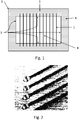
- Fig. 1 shows schematically a plurality of elongate electrical conductors 1 mounted to a lead frame 2 to form a conductor-frame assembly 3.
- the elongate electrical conductors 1 extend within a cavity 4 defined by walls 5 of the lead frame 2.
- the elongate electrical conductors 1 can be mounted to the lead frame by any convenient means (e.g. adhesively, by engagement with features on the lead frame, by brazing, welding or otherwise).
- Fig. 2 shows a picture of platinum wires bonded onto a Fe-Ni lead frame and Figs. 3 (a), (b), and (c) show details of such bonds. Details of why such a combination may be advantageous are presented below under the heading "The conductors and frame”.
- the conductor-frame assembly may be mounted in a die and the ceramic formed around the elongate electrical conductors 1 in the cavity 4.
- the fluid ceramic or ceramic precursor may be introduced through an aperture in the die, or through an optional aperture 6 formed in the lead frame 2, or both.
- the conductor-frame assemblies 3 may be stacked.
- Fig. 4 shows several conductor-frame assemblies 3 stacked adjacently to form a conductor frame so that the elongate electrical conductors 1 form a multilayered array of elongate electrical conductors 1. Subsequent forming of a ceramic body embedding part at least of the elongate electrical conductors 1 creates an assembled ceramic body having embedded parallel elongate electrical conductors 1. The assembled ceramic body can undergo processing while in the frame (which is removed subsequently), and/or after removal of the frame.
- the ceramic body may be a green ceramic body that is subsequently fired to sinter and densify the ceramic as described below.
- the separate conductor-frame assemblies 3 are shown stacked in a parallel relationship. This is not essential, particularly if it is desired that the conductors diverge from a first region on one face of the ceramic body to a second region of the ceramic body, the first region being smaller in area than the second region.
- Processing of the assembled ceramic body can include (without limitation) steps of drying, curing, sintering, annealing, or melting or a combination of two or more such steps, dependent on the nature of the ceramic used. Details of particular ceramics are presented below under the heading "The ceramic”.
- Processing of the assembled ceramic body can also include (without limitation) slicing the assembled ceramic body to form feedthroughs, polishing, exterior grinding (e.g. OD grinding, profile grinding), slicing, polishing (if required), metalization of surfaces that will be brazed, brazing, testing (e.g. hermeticity testing).
- slicing the assembled ceramic body to form feedthroughs, polishing, exterior grinding (e.g. OD grinding, profile grinding), slicing, polishing (if required), metalization of surfaces that will be brazed, brazing, testing (e.g. hermeticity testing).
- exterior grinding e.g. OD grinding, profile grinding
- slicing e.g. slicing, polishing (if required)
- metalization of surfaces that will be brazed e.g. hermeticity testing.
- brazing e.g. hermeticity testing
- a particularly useful process is to co-sinter a green ceramic body to form a monolithic dense ceramic body around the conductor.
- Co-sintering of metals like platinum e.g. platinum group metals [Pt, Ir, Os, Pd, Rh, Ru] or alloys thereof
- platinum group metals [Pt, Ir, Os, Pd, Rh, Ru] or alloys thereof) with oxide/non-oxide ceramics has been shown to occur without any surface deterioration of the metal phase provided that appropriate (e.g. non-oxidising) atmospheres are used during sintering to inhibit metal degradation.
- refractory metals e.g. platinum, molybdenum, nickel, tungsten, and their alloys
- do not react e.g. oxidize, nitride
- Such reactions can inhibit the performance (e.g. electrical conductivity and hermeticity) of the feedthrough, making these metals particularly suitable for use in feedthroughs.
- the sintering stresses from the ceramic matrix during the densification process causes the polycrystalline matrix to shrink and press on to the plastic surface of platinum or other refractory metal at the ceramic sintering temperatures (1050°C to 1800°C). This mechanical stress assures a strong mechanical bond between the metal and the ceramic matrix.
- full density it is meant a density of more than 90%, more than 94%, more than 98% or more than 99% theoretical density.
- the present disclosure is not limited to co-sintering but this technique is particularly useful.
- Figs. 6 and 7 show an approach that permits more complex conductor geometries to be achieved in which the elongate electrical conductors are in a non-layered relationship.
- elongate electrical conductors 1 are bonded at one end in a predefined pattern to a base plate/ring and the other ends are bonded to subsequent stacked lead frame parts/rings.
- the conductors are subsequently encapsulated in a self-supporting ceramic or ceramic precursor body yielding the 3D conductor architecture shown in Fig. 6(b) and 6(d) in which elongate electrical conductors 1 diverge from a base plane 7 to a number of positions displaced from the base plane 7.
- Fig 6(c) shows a typical process in more detail than Fig. 6(a) .
- first conductors 7 are each mounted by one end to a base plate 8 and by their other ends to a first frame layer 9.
- Second frame layer 10 is then stacked over first frame layer 9 and second conductors 11 mounted in like manner to both base plate 8 and second frame layer 10.
- the second conductors 11 may be mounted to the base plate 8 radially and/or rotationally displaced from the first conductors 7 to provide a desired separation; or may be mounted coincidentally with the first conductors 7, where a common connection is intended to be provided to the first conductors 7 and second conductors 11. The process is repeated with successive stacking of frame layers until a desired height is reached.
- the frame layers may be stacked directly on each other or with spacers lying between the frame layers. Further details of the frame layers may be found below under "The conductors and frame". As will be apparent to the skilled person, the frame may be stacked in a horizontal or a vertical fashion depending upon the design of the feedthrough desired.
- the frame parts are removed to leave a ceramic body 12 ( Fig. 6(d) ) including embedded electrical conductors. Removal of the frame parts may be mechanical (e.g. grinding away) or chemical (e.g. dissolution) or both, as appropriate for the materials used. Dependent on how mounted to the frame, the elongate electrical conductors may leave protruding parts 13, which can be useful in some applications.
- a feedthrough 14 is shown including a first face 14 and opposed second face 15. Elongate electrical conductors 1 diverge to form a non-collinear and non-coplanar 3D array. The elongate electrical conductors 1 diverge from a narrowly spaced 2D array 17 on the second face 15 to widely spaced 2D array 18 on first face 16 where they are terminated at contacts 19.
- the feedthrough 14 of Fig. 7 is shown mounted in a flange or ferrule 51.
- the feedthrough 14 is shown mounted to the flange or ferrule 51 with a brazed join 52.
- any alternative join may be used.
- the attachment of the feedthrough to a device may be made using the techniques described in US8,103,433 and/or US9,351,436 , which are hereby incorporated by reference.
- Fig. 8 (c) schematically illustrates the feedthrough 14 included in a device 53.
- a flange or ferrule is not used to attach the feedthrough 14 to the device 53.
- a flange or ferrule may be used, depending upon the design of the device 53.
- Figs. 9 (a) and (b) show a feedthrough 20 including two groups of elongate electrical conductors, the conductors in a first conductor group 21 being in a coplanar relationship defining a first group plane, and the conductors in a second conductor group 22 being in a coplanar relationship defining a second group plane.
- the conductors in first conductor group 21 are in parallel relationship to each other.
- the conductors in second conductor group 22 are also in a parallel relationship to each other. However, the conductors may be divergent within their respective group plane.
- the first group plane 21 includes 24 conductors. There are 14 further group planes parallel to the first group plane 21.
- the second group plane 22 includes 10 conductors. There are 5 further group planes parallel to the second group plane.
- individual ceramic bodies including embedded conductors may themselves be joined to form still more complex arrangements.
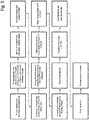
- Fig. 13 shows schematically a process for producing a conductor-frame assembly. This process includes
- the groups of frame parts with elongate electrical conductors provides a desired architecture, then the group of frame parts is passed on to further processing. If not, then the process is repeated with the product of one cycle forming the first frame group of the next cycle. During this process, optionally, electronic components can be mounted to the frame for embedding in the ceramic.
- the elongate electrical conductors may be of any suitable material, but particularly useful materials for use when co-sintering of the ceramic is required, are inert or refractory metals like platinum, niobium, iridium, nickel, etc. or alloys which are a combination of those. Platinum and 10%Ir/Pt have been used in the examples below. Accordingly, Pt or 0-15%Ir/Pt or 0-10%Ir/Pt or 8-12%Ir/Pt may be used to form the conductors. Pt, Ir, Nb, Pd, Au, Ni, Cr, W, Mo, Ta, Fe, Co, Ti, Rh, Re, Zr, V and their alloys may also be used for the conductors.
- a wide range of metals and alloys can form solid solutions with platinum.
- Fe-X Ni, Pd and Pt
- Fe-Ni alloys were chosen for the examples below, in particular 36%Ni+Fe, as they are inexpensive compared to the other two in the Invar family.
- Fe, Ni, Pd, Pt, Co, Cr, Al, Cu, Mo, Ta, W and their alloys may also be used.
- Fig. 2 shows Pt wires welded to a Fe-Ni frame.
- Figs. 3(a), (b), and (c) show scanning electron micrographs of the Pt-Invar interface at magnifications of 170X, 1200X and 12000X respectively, showing a good bond.
- Typical conductor diameters are 0.001 inch to 0.040 inch. For example, 0.0005 inch, 0.001 inch, 0.002 inch, 0.005 inch, 0.010 inch, 0.020 inch, 0.030 inch, or 0.040 inch. Typical conductor ranges include any of these values, for example, 0.0005 inch to 0.005 inch, 0.0005 inch to 0.002 inch, 0.0005 inch to 0.001 inch, 0.001 inch to 0.002 inch.
- Frame parts to which the elongate conductors are mounted, and spacers between adjacent frame parts, may include recesses to accommodate parts of the conductors lying between adjacent frame parts.
- the frame and frame parts may each include a single body of material to which the conductors are bonded, or a composite body including regions of material to which the conductors may be bonded, and regions of material not capable of being bonded to the conductors.
- Fig. 14 shows conductor-frame assembly 3 similar to that of Fig 1, but in which a non-conductive lead frame 33 carries metallic pads 34, which may be either surface mounted or embedded in the non-conductive lead frame 33, and in which the elongate conductors are mounted to the metallic pads 34.
- Fig. 15 shows conductors 1 mounted to a frame in a closely mounted region 35, and further apart in a widely mounted region 36 and then, after forming the ceramic body, removing the surface of the body to expose a plane of desired conductor spacing 37.
- Solid conductors having a circular cross-section may be used.
- conductors are available as wire, they may be economic.
- the avoidance of angular geometries e.g. ellipsoidal
- other cross-sectional shapes may be used.
- hollow conductors may be used in the method to provide feedthroughs having hollow conductors.
- Typical ceramics and composites include, but are not limited to, BN, B4C, Si3N4, TiC, TiN, TaN, A12O3, ZrO2, SiO2, MgO, ZnO, CaO, BeO, MnO, Y2O3, Nb2O5, Cr2O3, SnO2, MnO2, TaO, CuZO, BeO, NiO and other lanthanide oxides or a combination, of two or more of these in the form of a compound like spinel or glass ceramics like Macor® or a solid solution.
- the present disclosure also contemplates the use of glasses and glass ceramics.
- a non-glass based ceramic may be desirable.
- certain glasses may react with human or animal bodily fluids reducing the biostability of the feedthrough. Therefore, non-glassed based ceramics may be chosen in order to increase biostability of the formed feedthrough.
- the ceramic can be formed around the elongate electrical conductors by any suitable process giving the degree of bonding and hermeticity required by the intended application.
- Typical processes include, slip casting, gel casting, low pressure-low viscosity thermoplastic injection moulding, fluidized bed direct transfer, low stress casting, zero pressure casting, casting by gravity feed, casting without application of external pressure, and other alternatives that will be apparent to the skilled person.
- the processes do not expose the elongate electrical conductors to significant pressure, which may lead to distortion and misalignment.
- the processes are performed at less than 2 atmosphere (absolute), more preferably under ambient atmosphere and even more preferably under vacuum.
- Desirable features to achieve high density and hermeticity in a composite body are:
- a co-sintering process may be used to densify a green body in which the ceramic matrix encapsulates the metal pin array.
- the selection of the co-sintering process parameters are dependent on the metal-ceramic system chosen. Typically, the temperature can range from 1050°C to 1800°C for the peak sintering temperatures.
- the environment can also change from air atmosphere to inert to other atmosphere or vacuum.
- a binder if a binder is used the green monoliths can be run through an air oven for binder burn-out and subsequently transferred to a high temperature furnace for sintering. In some cases, pressure assisted sintering may also be used.
- FIG. 10 shows the overall process up to and including embedding the elongate electrical conductors 1 in ceramic.
- Platinum wires 1 were bonded to a conductor-frame assembly precursors 24, 25, 26 using the wire bonding process.
- the individual lead frames 25, 26, 27 were then arranged into the desired pattern to form an assembly 28 of lead frames 25, 26, 27.
- the assembly 28 was then placed in a mould/die (indicated schematically at 29) and followed by the casting of the ceramic matrix using a gel-casting approach.
- Gel casting of alumina was accomplished as follows: A 99.9% pure alumina slurry was made with acrylic dispersant and water followed by the addition of a monomer methacrylamide and cross-linker polyethyleneglycoldimethylacrylate. The solids loading of the alumina was about 40 vol.%
- Gel casting approaches may be used, as will be apparent to the skilled person.
- Gel casting methods which produce zirconia ceramics, zirconia toughened alumina (ZTA) ceramics, yttria-tetragonal zirconia polycrystal (3Y-TZP) alumina ceramics, and/or other ceramics may be used.
- ZTA zirconia toughened alumina
- Y-TZP yttria-tetragonal zirconia polycrystal
- the individual feedthroughs 20 are subsequently diced out of the co-fired monolith or in other cases may be over-moulded individually based on the design.
- This process permits extremely thin ( ⁇ 400 ⁇ m) insulator plates to be made with integral conductors running therethrough in a closely spaced ( ⁇ 250 ⁇ m spacing) relationship.
- a known alternative to the ceramic laminate of Fig. 23 is the use of a platinum ink which has similar problems to a ceramic laminate.
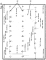
- Fig. 11 shows a cut section of a high density feedthrough made by this process, using 50 ⁇ m [ ⁇ 0.002 inch] diameter platinum conductors 31 embedded in a monolithic alumina matrix 32.
- the conductors are arranged in layers, and shown are measurements made of conductor positions.
- This figure shows that the process of the present disclosure is readily able to achieve a conductor to conductor pitch within a layer of approximately 250 ⁇ m [9.22 thou ⁇ 234 ⁇ m] with a standard deviation of less than 25 ⁇ m [0.962 thou ⁇ 24.4 ⁇ m].
- Interlayer spacing is determined by the lead frame thickness and any spacing between lead frames, and this example is not optimised for close spacing.
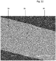
- Fig. 12 shows that the phase boundary 35 between the platinum and the alumina matrix is clean, showing no signs of chemical diffusion or metal deterioration.
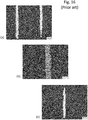
- Fig. 16 shows a prior art feedthrough including a metallic conductor within a ceramic matrix.
- the feedthrough was prepared according to the method of US8,698,006 .
- Figs. 16(a), 16(b) and 16(c) show images wherein the surface of the conductor has been polished to differing depths. As is apparent, the surface shown is in the plane of the conductor.
- the conductor is approximately 0.002 inch (50 ⁇ m) in diameter. Whilst using the method of US8,698,006 it was desired to achieve a conductor having a uniform cross-section, however, it can be seen that the cross-section is not uniform as the edges of the conductor are jagged or have a zigzag profile. It is therefore apparent that the conductors do not have a smooth or uniform surface. As shown in Fig 16 , the deviation due to slip/distortion can be up to 25 ⁇ m for a 50 ⁇ m pin.
- Fig 17 shows a feedthrough including a metallic conductor within a ceramic matrix prepared using the present method.
- ZTA ceramic matrix
- the visible porosity and scrub-offs are artefacts of the polishing process and not features of the feedthrough. Nevertheless, it is clear that the wires are not zig-zagged.
- Figs. 18 and 19 are CT Scans (X-rays) of 0.002 inch diameter wires 1 in ZTA ceramic matrix 12.
- the length of the image in Fig. 18 is about 2.4 mm (0.1 inch).
- the shadows and light pattern of the wires are an artefact of the X-ray technique which makes the diameter of the wires appear slightly larger than reality. However, it can clearly be seen that the wires are virtually parallel and straight over the entire visible 2.4 mm length.
- Figure 19 shows the in-plane positional accuracy is approximately within 0.0005 inch, which is discussed in more detail below with reference to Figs. 20 to 22 .
- Fig. 20 shows a conductor position tolerance of +/- 50 microns with a conductor diameter of 50 microns.
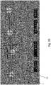
- Pt pins 1 having a diameter of 0.002 inch are shown in a ZrO2 insulating ceramic 12. The surface is diced and unpolished. The solid lines correspond to a "perfect" or desired position and the dotted lines correspond to the measured position. These measurements demonstrate deviation from the desired position of ⁇ 0.0005 inch within y-plane (left right as shown in Fig. 20 ). These measurements also demonstrate deviation from the desired position of ⁇ 0.0008 inch within x-plane (up down as shown in Fig. 20 ).
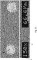
- Fig. 21 shows 2 thou diameter Pt pins in ZrO 2 ceramic body. The surface is diced and unpolished. In Fig. 21 the majority of deviation from "perfect" or desired position (indicated by dotted line) is a result of surface condition artifacts from dicing process due to soft nature of Pt. The deviation from the desired position is ⁇ 0.0002 inch.
- Fig 22 shows 0.015 inch diameter Pt pins in ZTA ceramic body. Again, the surface is diced and unpolished. In this example, no deviation from "perfect" or desired position is observable.
- conductor-to-conductor spacings of 235 microns (235 ⁇ m, 9.2 thou) has been demonstrated. In other examples conductor-to-conductor spacings of 200 microns (200 ⁇ m, 7.9 thou) has been demonstrated. In yet further examples, conductor-to-conductor spacings of 135 microns (135 ⁇ m, 5.3 thou) has been demonstrated. In another example, conductor-to-conductor spacings of 100 microns (100 ⁇ m, 3.9 thou) has been achieved. These spacings correspond to conductor densities of 1 conductor per 85 thou 2 , 1 conductor per 62 thou 2 , 1 conductor per 28 thou 2 , and 1 conductor per 15 thou 2 , respectively.
- conductor spacings of the order of 4.8 thou or less corresponding to conductor densities of 1 conductor per 23 thou 2 have been achieved.
- conductor spacings of 90 microns (90 ⁇ m, 3.5 thou) corresponding to conductor densities of 1 conductor per 12 thou 2 can be achieved using the described methods.
- Conductors having a diameter as small as 0,002 inch have been used in the described method to form a feedthrough. It is anticipated that conductors having a thicknesses as small as 0.001 inch may readily be used in the described method to form a feedthrough. Further, it is expected that conductors thinner than 0.001 inch may be used in the described method to form a feedthrough.
- thicker conductors may be preferred.
- the conductors when they are thicker they may support greater electrical requirements. For example, greater voltages and/or current requirements.
- Fig. 12 shows a polished cross section of a 380 ⁇ m (15 mils) diameter platinum pin 33 co-sintered in an alumina matrix 34.
- Figs. 11 and 12 show that the present disclosure enables use of multiple sized conductors (wires/pins) embedded and co-sintered in a fully dense ceramic matrix which is hermetic through the length of the embedded conductors.
- the standard dimension and high density feedthroughs made through this process are hermetic to ⁇ 1x10 -9 mbar-l/sec after the thermal shock (-60°C to 200°C 5 cycles).
- a hermeticity of ⁇ 1x10 -10 mbar-l/sec was measured.
- a hermeticity of ⁇ 1x10 -11 mbar-l/sec was measured.
- test method 1014 and test condition A 4 was employed.
- feedthroughs having thicknesses ranging from 750 microns (750 ⁇ m, 30 thou) to 1.6 mm (63 thou) have been prepared. These feedthroughs have good hermeticity, as described above.
- FIG. 25 A mathematical method for determining conductor densities is illustrated with reference to Fig. 25 .
- Fig. 25 four conductors 1 are shown. The view is that of a cross-section through a feedthrough.
- the conductor density could similarly be calculated using the square having sides c and d (which is equal in size to the square having sides a and b).
- feedthroughs with high densities over large cross-sectional areas. For example, areas greater than 23, 100, 250, 500, 1000, 2000, 4000, 6000, 10000 thou 2 .
Landscapes
- Health & Medical Sciences (AREA)
- Public Health (AREA)
- Nuclear Medicine, Radiotherapy & Molecular Imaging (AREA)
- Radiology & Medical Imaging (AREA)
- Life Sciences & Earth Sciences (AREA)
- Animal Behavior & Ethology (AREA)
- General Health & Medical Sciences (AREA)
- Engineering & Computer Science (AREA)
- Biomedical Technology (AREA)
- Veterinary Medicine (AREA)
- Compositions Of Oxide Ceramics (AREA)
- Fuel-Injection Apparatus (AREA)
- Prostheses (AREA)
- Container, Conveyance, Adherence, Positioning, Of Wafer (AREA)
- Vessels And Coating Films For Discharge Lamps (AREA)
- Superconductors And Manufacturing Methods Therefor (AREA)
- Coupling Device And Connection With Printed Circuit (AREA)
- Insulating Bodies (AREA)
- Electrotherapy Devices (AREA)
Abstract
There is provided a feedthrough including a ceramic body; and a plurality of electrical conductors embedded in the ceramic body. Wherein the density of the electrical conductors exceeds 1 conductor per 23 thou2 through a planar cross-section of the ceramic body.
Description
- This disclosure relates to feedthroughs including electrical conductors at least in part embedded in a ceramic matrix. The present disclosure further provides methods of making such feedthroughs.
- Metal ceramic assemblies are required for many applications, and have found particular use in applications where one or more electrical conductors are required to pass through a ceramic insulator to provide one or more electrically conductive connections from one surface of the ceramic insulator to another surface of the ceramic insulator. Such an arrangement of a conductor passing through an insulator is commonly known as a "feedthrough". Such arrangements are widely used, for example in medical, aerospace, transportation, communication and power tube (e.g. x-ray, radio frequency) applications, and the present disclosure is not limited to any one application.
- While the present disclosure is generally applicable, its impact can be seen by reference to a particularly demanding application, namely the provision of braze-free hermetic feedthroughs for medical applications.
- Electronic biomedical implants are being increasingly used to diagnose, prevent and treat diseases and other conditions. Such implanted devices are typically housed in hermetic packages that incorporate electrical feedthroughs for signal transfer between the housed electronic device and the environment. Such implantable devices, especially those that interface with the human nervous system, the cochlea, or the retina, require a multiplex of leads in a very small feedthrough.
- Biocompatible metal ceramic feedthrough systems may be considered to be the most reliable choice for such devices owing to their inertness (e.g. biocompatibility) and longevity (e.g. biostability).
- For certain therapies, it is desirable to increase the number of electrical conductors (which have many names in the art of feedthroughs including: leads, pathways, pins, wires, and vias) in the feedthroughs to increase the number of I/O signals. However, it is simultaneously desirable to decrease the size of the feedthrough as it is not desirable to implant a large device (including a large feedthrough) in to the human or animal body. In particular, it is desirable to reduce the invasiveness of the implantation surgeries and/or the nature of the placement of the device for the target therapy requires a small device, such as retinal implants. When the device design requires both a large number of conductors (i.e. high pin count) and a small size feedthrough, conventional feedthrough manufacturing techniques are no longer viable.
- It is therefore desirable to increase the density of the conductors within feedthroughs. However, existing technologies have limits as to the spacing of conductors within the feedthrough. Therefore, until now, it has been necessary either to make the feedthrough larger (and therefore also a device including the feedthrough) or to reduce the number of I/O signals, both of which are undesirable.
- It is a non-exclusive aim of the present disclosure to provide cost effective miniaturization of a biocompatible, biostable co-fired feedthrough. It is a further non-exclusive aim of the present disclosure to provide novel three-dimensional architectures. It is an additional non-exclusive aim of the present disclosure to provide a cost effective method of manufacture of feedthroughs. Conventional gold brazed feedthrough technologies are capable of providing conductor-to-conductor spacings as close as 0.022 inch (") using 0.004" diameter wires with gold braze rings. Additionally, using manual techniques of placing electrically conductive wire (e.g. pins) with gold braze rings into preformed (e.g. drilled, pressed, stamped) holes within an electrically insulative member (typically a high purity alumina ceramic) to construct the feedthrough with a high number of leads is costly and increases the opportunity for errors leading potentially to high scrap rates. Besides the challenge of constructing such a feedthrough by hand, a current practice of utilizing a gold braze ring to assist in achieving a hermetic bond between the metallic pin and the insulator is design limiting. The thickness of this gold ring adds a design constraint and limits the proximity that the conductors can be placed in proximity to each other. This limits the density of the conductors and therefore constrains the degree to which the feedthrough can be miniaturized.
- It has been proposed to make feedthroughs using a tape casting/layer by layer stacking process. Here thin ceramic tapes are first processed to have through holes which are then filled with a metal or ceramic-metal ("cermet") ink. These tapes are then aligned and stacked together and subsequently co-fired to produce a feedthrough with the aligned filled holes forming the conductive pathways. This technology has dimensional limitations to the feature size and shape (in this example holes that are cut in individual tapes). Also, since the holes are filled with a metal/cermet ink, there can be spillage around the surface edges, which tend to protrude out from the conductive via-path in the sintered state. This reduces the effective conductive pathway to conductive pathway distance to less than the design separation to assure insulative isolation, causing possible areas for electrical failure (e.g. an electrical short or arc) of the device. Such spillage may also act as a structural defect which may elongate if thermally cycled leading to loss in hermeticity and potential delamination. The manufacturing of feedthroughs with this technology is also process intensive thus increasing cost. Further, the use of particulate ink
- (metal/cermet) in this technology leads to potential issues during the I/O termination/connections to other electronic components especially in the high density or miniature scale devices. Also, the use of a non-metal filler within the conductive pathway increases the electrical resistance of the pathway (e.g. reducing the electrical conductivity) reducing the electrical efficiency of the device, requiring more energy than would otherwise be necessary, resulting either in the need for a larger battery to achieve the required device lifetime (thus constraining the miniaturization of the device), or resulting in reduced lifetime for a given battery size (thus limiting the lifetime of the device).
- Some known examples of feedthroughs and techniques for providing feedthroughs for such medical application include:-
-
US8,698,006 (US'006) discloses feedthroughs including:- a. an insulative component; and
- b. first and second conductors electrically isolated from each other by the insulative component.
- A density of 1 conductor per 24 thou2 (i.e. 0.000024 square inches) is disclosed in
Figure 19 . - The method of US'006 includes forming a feedthrough by:-
- a. providing a first insulative component with at least one bonding surface;
- b. providing a second insulative component;
- c. disposing a conductor between the first and second insulative components and along at least a portion of the bonding surface;
- d. bonding the first and second insulative components at the bonding surface; and
- e. exposing a portion of the conductor.
- A problem with the method and feedthroughs of US'006 is that the pressing force causes the conductor to deform, forming a tortuous (e.g. zigzag) profile that reduces the conductive efficiency of the conductive pathway. Also, without a method to fix the conductors in place during the pressing operation, the conductors can move, resulting in positional inaccuracies of the conductive paths, complicating subsequent attachment of the conductive paths to a device and/or to leads. Further, producing a hermetic bond between the insulative component and the electrically conductive wire becomes increasingly difficult as the size of the diameter of the wire is increased above 0.003 inch, effectively limiting the maximum size of the wire that can be used. Lastly, the minimum thickness of the thinnest green ceramic plates that can be produced and placed between the rows of pins, limits the minimum spacing of these rows of pins to each other to 0.016".
-
US7,988,507 (US'507) discloses a feedthrough for an implantable medical device including: - an electrically insulating body including a first surface and a second surface; and
- one or more electrically conductive structures configured to contiguously extend through and be embedded within said electrically insulating body, such that each of said one or more electrically conductive structures are circumferentially covered by said electrically insulating body, such that opposing ends of said at least one electrically conductive structures are exposed, and such that said at least one electrically conductive structures extend beyond at least the first or second surface,
- wherein the one or more electrically conductive structures include an electrically conductive metal or metal alloy and have a thickness of a film of the same electrically conductive metal or metal alloy.
- US'507 also discloses a method of forming an electrically conducting feedthrough including the steps of:
- (i) forming an electrically conductive structure including a sacrificial component and non-sacrificial component;
- (ii) coating at least a portion of the non-sacrificial component with a relatively electrically insulating material; and
- (iii) removing at least a portion of the sacrificial component from the electrically conductive structure,
- The coating step (ii) includes moulding a coating of the insulating material on and/or around the conductive structure and in a preferred embodiment used powder injection moulding (PIM) to mould the insulating material around a desired portion of the conductive structure.
- Problems with the process of US'507 include that for medical applications noble metals (e.g. platinum) are the desired conductors and the sacrificial part of the platinum foils used results in waste material requiring expensive recycling. Further, when stamping platinum from a foil the individual conductors can be embrittled in the stamping process, limiting the diameter of conductors that can be formed. Further still, a stamping process requires the use of precision stamping dies for each geometry of feedthrough. Yet further, when sections of a foil are removed within a foil, the remaining sections within the foil can sag or flex because residual stresses have been relieved from the foil by removing material and because the removal of mass has reduced the stiffness of the remaining foil sections. This sagging by itself, or deflection of the remaining material when subjected to the subsequent molding pressure, can result in positional inaccuracies of the conductive paths, complicating subsequent attachment of the conductors to a device and/or to leads.
- The methods of US'507 and US'006 limit the arrangement of conductors to essentially parallel layers of conductors. The limitation to essentially parallel arrangements of conductors limits the conductor pathways that can be achieved. This means that additional circuitry external of the feedthrough may be required.
-
US2013/0032382 (US'382) discloses a hermetic feedthrough for an implantable device, including:
Stacked sheets of electrically insulative ceramic alumina, each sheet containing a hole(s) that are substantially aligned with one another to form a conductive path through the sheets via the holes filled with an electrically conductive substance; the sheets and the conductive substance having a co-fired bond between the sheets and that hermetically seals the hole. - US'382 also discloses that the resulting tortuous (e.g. staggered, serpentine, zigzag) path of the resulting vias improves the hermetic seal of the feedthrough by better impeding fluid from seeping along the via. However, this benefit may be offset by the same tortuous path increasing resistance to electrical current, decreasing the efficiency of the device to which the feedthrough is attached versus an otherwise straight via.
- US'382 limits its examples to holes of 0.006" - 0.008" diameter, with via lengths of 0.042" to 0.066" length with pitch of -0.0181" having passed a He leak test. However, only a hole of 0.008" diameter and of length 0.042" and a minimum pitch of ∼0.028" was illustrated to exhibit no dye penetration.
- A minimum pitch of 18.1 thou (0.0181 inch) corresponds to 1 conductor per 328 thou2.
-
US7,480,988 (US'988),US7,989,080 (US'080),US8,163,397 (US'397), andUS5,272,283 (US'283) describe feedthroughs having metal tubes (acting as the conducting path) co-fired to a ceramic insulator whereby a (hermetic) seal by compression of the tube is achieved as the ceramic shrinks when the assembly is fired and then allowed to cool. Although perhaps effective when using tubes with diameters exceeding >0.040 inch and ceramic sheet at least 0.70 inch thick, smaller tube diameters are impractical, limiting the smallest possible feedthrough geometry. - US'283 discloses that it is not possible to produce a co-fired feedthrough with a high number of conductive pathways (cited as typically 10-22).
- US'988, US'080, and US'397 also disclose that feedthroughs relying upon ceramic insulators consisting of 92% or 96% alumina with significant glass content. However the glass is susceptible to hydroxide etching. This etching chemical reaction may result when the ceramic/glass feedthrough is exposed to an aqueous chloride environment such as found in the human body. Further discussion of this phenomenon is described in patent
US 9,698,662 - US'988, US'080, and US'397 also describe a method of producing a hermetic feedthrough consisting of a ceramic sheet less than 0.040" thick containing drilled blind holes into which metal wires with diameters of less than 0.010" are inserted and then subsequently co-fired to achieve the hermetic seal, however, no hermetic values are presented. After firing the ceramic is lapped on the blind hold side to expose the wires for the purpose of achieving an electrically conductive pathway through the insulating ceramic. A helium leak test is performed, although the documents are silent whether a dye penetrant test has been conducted. Singulation (dicing) then follows to form the exterior periphery of the individual feedthroughs. The documents are silent regarding the nearest spacing of the resulting conductors that has been achieved by this approach. The documents are also silent regarding the insertion method employed. It is reasonable to anticipate that the method of pin insertion is manual, requiring labor to place and fixturing to hold such small, lightweight, delicate pins in place during the co-sintering operation. This also potentially requires high labor costs and results in poor yields. There is a practical limit to how close pins can be placed to each other using manual techniques. Further, grinding of the fired ceramic to expose the metal wire (in order to attach to electrical connection pathways) adds cost. Yet further, the examples are limited to a parallel array of wires.
-
US8,277,227 (US'227) discloses fabrication of feedthroughs by inserting conductive pins (wires) into an unsintered (or 'green') ceramic and then co-firing (such as described by US'988, US'080, and US'397). The hand assembly of US'227 leads to inaccuracies, is time consuming (labor intensive and therefore relatively expensive), and can result in unsatisfactory leak rates on testing and result in poor yields. It seems that the methods of US'988, US'080, and US'397 also include such hand assembly. Additionally, the resulting position of the co-fired pins lacks precision as it is dependent on the manual process. This can present subsequent difficulties in integration of the I/O in an implantable device. This lack of precision also necessarily limits the maximum achievable density of pins within a feedthrough. - US'227 also discloses that cochlear implants typically rely upon feedthroughs containing 22-24 conductive pins with a desire to increase the number of pins while reducing the size of feedthrough. A high degree of labour intensity and specialisation such as backface grinding in order to expose the wire can raise manufacturing problems. Thus, US'227 discloses a method to achieve such a co-fired feedthrough which is reliant upon a thin conductive film to form the conductive pathways that are not dependent upon such labor intensive processes to place the wires. However, US'227 provides few details of the hermeticity values and dye penetrant results obtained, size boundaries of the conductive pathways, spacing boundaries between pathways, parallelism or positional accuracy of the conductive pathways.
- US'227 does provide the relationship: H= f (L, 1/A, 1/t) where H represents hermeticity, L is the length of the electrically conductive element measured form the first face to the second face of the insulative portion of the feedthrough, A is the cross-sectional area of the electrically conductive element, and t is the time that the interface is exposed to the fluid such as body fluid. The formula implies feedthroughs with thick cross sections with small conductive via diameters (or cross sections if the conductive pathway is not circular in cross section) will have improved hermeticity versus thin feedthroughs with large diameter conductive pathways.
- US'227 discloses a thickness of the conductive members being 0.040" to 0.070" but does not disclose the width of the conductors, hermeticity or dye penetrant results nor thickness of the feedthrough, nor resulting positional accuracy or closest spacing of the conductive elements. However, US'227 discloses the use of shaped (e.g. stepped or screw-thread shape) conductive members to improve hermeticity, it must, therefore, be assumed that without shaping the conductive members the hermeticity is insufficient.
- It is a non-exclusive object of the present specification to provide improved feedthroughs. The improved feedthroughs may address, at least partially, the disadvantages realised in the prior art (as discussed above). The improved feedthroughs of this specification may be provided by new feedthrough manufacturing methods disclosed herein. These feedthrough manufacturing methods may address, at least partially, the disadvantages realised in the prior art (as discussed above).
- It is a (non-exclusive) aim of this specification to provide methods capable of forming hermetic feedthroughs having a small inter-conductor separation; methods capable of providing arrangements of conductors not limited to layers; methods that can be repurposed without the need for precision stamping dies; methods that can produce non-tortuous conductive pathways; and/or methods that can provides an array of conductors that are accurately and/or precisely positioned.
- It is also a (non-exclusive) aim of this specification to provide hermetic feedthroughs having a small inter-conductor separation; feedthroughs including conductors not limited to layers; feedthroughs including non-tortuous conductors; and/or feedthroughs including an array of conductors that are positioned accurately and/or precisely.
- The feedthroughs may be biocompatible. The feedthroughs may be hermetic. In particular, the feedthroughs may be implantable with a human or animal body. Advantageously, the feedthrough may be able to withstand the chemical reactions that can occur within the human body. For example, the feedthrough may remain hermetic for the life of the implant. For example from one to 20 years or more.
- It is also a (non-exclusive) aim of this specification to provide feedthroughs having straight, solid, metal wire of a range of diameters. Larger diameter wires can provide increased electrical conductivity efficiency.
- It is also a (non-exclusive) aim of this specification to provide methods which do not rely upon insertion of individual wires into a green ceramic nor post grinding the fired ceramic to expose the wire to the feedthrough surface (which may be costly). In other words, it is (non-exclusive) aim to automate the placement of the conductors. Further, it is a (non-exclusive) aim to produce thin profiles and place wires easily in close proximity to each other with accurate positioning.
- It is a further (non-exclusive) aim of this specification to provide methods which can be implemented by robot (instead of manually). Such implementation can reduce labour costs and improve device yield. Further, robotic construction may be particularly suited to the use of thin, closely packed conductors and the provision of miniature feedthroughs.
- It is a further (non-exclusive) aim of this specification to eliminate the need to use gold braze rings around the conductors. Removing the need to use a gold braze ring can help alleviate dimensional constraints. Eliminating the ring can reduce required spacing allowing miniaturization of the feedthrough. Further, in the prior art, under certain conditions the gold can electro-migrate leading to a loss of a hermetic seal. Directly bonding the conductor to the insulator without the use of a gold braze can eliminate (or reduce the risk of) electro migration potential, this can improve the long-term hermeticity (and therefore biostability) of the feedthrough. Yet further, elimination of the need to use a gold braze ring can remove the need for a cost involved in the production of the feedthrough.
- The methods disclosed herein are useful for providing high-pin count and/or miniature feedthroughs. Additionally, the methods disclosed herein are also useful for providing low-pin count feedthroughs and/or non-miniature feedthroughs. Further, whilst prior art methods of feedthrough construction permit a two-dimensional arrangement of conductors, the methods disclosed herein can enable a three-dimensional arrangement of conductors.
- Further, as the methods and feedthroughs of the present specification can use solid metal wire conductors, instead of metallic paste with a ceramic additive (or alternatives), conductors with low electrical resistance can be provided within the feedthroughs. In turn this can increase device battery life or allow the use of smaller batteries. Increased battery life can reduce the number of surgeries required by reducing the number of times a medical device has to be replaced. Yet further, a conductive pathway with lower electrical resistance permits the designer of a feedthrough to specify a conductor with a smaller diameter, potentially allowing further miniaturization of the feedthrough and a smaller battery allowing further miniaturization of the implanted device.
- Yet further, the methods disclosed herein can provide devices having a non-tortuous profile of the conductor. This can provide a low electrical resistance of the conductive path (preserving the ability to specify a small conductive pathway diameter), prevent or reduce the likelihood of formation of potential stress risers (that can lead to loss of a hermetic seal), and prevent or reduce the likelihood of short-circuit pathways between conductors. This contrasts with prior art methods in which wires are deformed during the feedthrough fabrication processes, which can result in a torturous (e.g. zigzag) conductive pathways or processes. Such processes typically rely upon pastes or inks which can seep between ceramic layers (e.g. tape layers) of the insulating member (thereby providing non-desirable short-circuit pathways).
- A further potential benefit of the methods and devices disclosed herein is the positional accuracy of the conductive paths in contrast to prior art fabrication processes that rely upon molding pressure (e.g. compression, injection molding). In the prior art, upon application of a molding pressure conductive pathways can move or deflect. In turn, this can alter the position of the conductors complicating subsequent attachment of the feedthrough conductors to the device and/or to the leads. Movement of the pathways may also undermine the electrical resistance of the insulating member by reducing the distance between adjacent conductive pathways. To account for such movement using such processes, the minimum pathway design distance between pathways must be increased, hindering optimal miniaturize the feedthrough. Accordingly, a (non-exclusive) aim of the present disclosure is the provision of fabrication methods that do not require the application of (significant) molding pressures, which can move or deflect the conductors of a feedthrough.
- It is a further (non-exclusive) aim of the present disclosure to provide a method which can be used (cost-effectively) with a range of diameters of conductors. As will be apparent, such methods may be used to provide a range of feedthroughs having a range of conductor diameters. Prior art feedthrough fabrication methods that rely on compressive force to sandwich conductive wires between green ceramic insulating sheets can experience an upper limit of wire diameter that can be successfully pressed. Feedthrough fabrication methods that rely on insertion of small diameter wires into preformed holes within an insulating ceramic can experience high labor costs and poor yields due the delicate nature of the wires that may bend during insertion. Providing methods which can be used with a variety of conductors is advantageous as small diameter wires may be required to achieve certain degree of miniaturization, while large diameter wires may be a necessity for devices that require transmission of signals of higher voltage.
- Accordingly, there is provided a feedthrough including:
- a ceramic body; and
- a plurality of electrical conductors embedded in the ceramic body, wherein the density of the electrical conductors exceeds 1 conductor per 23 thou2 through a planar cross-section of the ceramic body.
- The density of the electrical conductors preferably exceeds 1 conductor per 22 thou2, or exceeds 1 conductor per 21 thou2, or exceeds 1 conductor per 20 thou2, or exceeds 1 conductor per 19 thou2, or exceeds 1 conductor per 18 thou2, or exceeds 1 conductor per 17 thou2, through a planar cross-section of the ceramic body.
- Each of the plurality of electrical conductors may be parallel relative to each other within 2°. Further, each of the plurality of electrical conductors may be parallel to each other within 1.5°, 1°, 0.5° or 0.2°.
- There is also provided a feedthrough including a plurality of electrical conductors embedded in a ceramic body, in which the plurality of elongate electrical conductors traverse the ceramic body in a non-coplanar relationship.
- The plurality of elongate electrical conductors may include at least one planar array of elongate electrical conductors defining a plane, and at least one elongate electrical conductor non-parallel with said plane.
- The plurality of elongate electrical conductors may include at least two groups of elongate electrical conductors, the conductors in each group being in a coplanar relationship to define a group plane, and in which the group planes of at least two of the plurality of groups are non-parallel.
- The plurality of elongate electrical conductors may include at least one group of elongate electrical conductors diverging from a first region of the ceramic body to a second region of the ceramic body, the first region being smaller in area than the second region.
- The ceramic body may include one or more walls extending from a base, and at least one of said plurality of elongate electrical conductors may be mounted to traverse the ceramic body from the base to said one or more walls.
- At least two of said plurality of elongate electrical conductors may be mounted non-parallelly to traverse the ceramic body diverging from the base to said one or more walls.
- Each of the plurality of electrical conductors may be substantially straight along the length of the conductor within the ceramic body.
- The plurality of electrical conductors may include a first electrical conductor; a second electrical conductor; a third electrical conductor; a fourth electrical conductor; and/or a fifth electrical conductor.
- There is also provided a feedthrough including:
- a ceramic body;
- a first electrical conductor embedded in the ceramic body; and
- a second electrical conductor embedded in the ceramic body, wherein a surface of the first electrical conductor is within 0.0038 inch of a surface of the second electrical conductor.
- There is also provided a feedthrough including:
- a ceramic body; and
- a first electrical conductor embedded in the ceramic body,
- There is also provided a feedthrough including:
- a ceramic body; and
- a first electrical conductor embedded in the ceramic body,
- The hermeticity of the feedthrough may be <1x10-11 mbar-l/sec.
- There is also provided a feedthrough including:
- a ceramic body; and
- a first electrical conductor embedded in the ceramic body,
- Preferably, the density of the ceramic body is at least 96% or at least 97% or at least 98% or at least 98.5% of the theoretical bulk density. Preferably, the standard deviation is less than 0.5% or less than 0.4% or less than 0.3% or less than 0.2%.
- There is also provided a feedthrough including:
- a ceramic body;
- a first electrical conductor embedded in the ceramic body; and
- a second electrical conductor embedded in the ceramic body,
- There is also provided a feedthrough including:
- a ceramic body;
- a first electrical conductor embedded in the ceramic body;
- a second electrical conductor embedded in the ceramic body; and
- a third electrical conductor embedded in the ceramic body,
- There is also provided a feedthrough including:
- a ceramic body;
- a first electrical conductor embedded in the ceramic body;
- a second electrical conductor embedded in the ceramic body; and
- a third electrical conductor embedded in the ceramic body,
- A surface of the first electrical conductor may be within 0.0038 inch of a surface of the second electrical conductor along the whole length of the first and second conductor within the ceramic matrix within a tolerance of ±5% or 0.002" which ever is greater.
- The tolerance may be measured relative to the largest distance. The tolerance may be measured relative to the average distance.
- The surface of each of the plurality of electrical conductors may be smooth. The surface of the first, second, third, fourth and/or fifth electrical conductor may be smooth.
- Each of the plurality of electrical conductors may be straight or linear. The first, second, third, fourth and/or fifth electrical conductor may be straight or linear.
- Each of the plurality of electrical conductors may be straight or linear along the portion within the ceramic body. The first, second, third, fourth and/or fifth electrical conductor may be straight or linear along the portion within the ceramic body.
- Each of the plurality of electrical conductors may have a substantially constant cross-section. The first, second, third, fourth and/or fifth electrical conductor may have a substantially constant cross-section.
- Each of the plurality of electrical conductors may have a solid cross-section. The first, second, third, fourth and/or fifth electrical conductor may have a solid cross-section.
- Each of the plurality of electrical conductors may have a substantially constant cross-section along the portion within the ceramic body. The first, second, third, fourth and/or fifth electrical conductor may have a substantially constant cross-section along the portion within the ceramic body.
- Each of the plurality of electrical conductors may have a solid cross-section along the portion within the ceramic body. The first, second, third, fourth and/or fifth electrical conductor may have a solid cross-section along the portion within the ceramic body.
- Each of the plurality of electrical conductors may have a hollow cross-section. The first, second, third, fourth and/or fifth electrical conductor may have a hollow cross-section.
- Each of the plurality of electrical conductors may have a hollow cross-section along the portion within the ceramic body. The first, second, third, fourth and/or fifth electrical conductor may have a hollow cross-section along the portion within the ceramic body.
- Each of the plurality of electrical conductors may be parallel to each other within 2°. Each of the plurality of electrical conductors may be parallel to each other within 1.5°. Each of the plurality of electrical conductors may be parallel to each other within 1°. Each of the plurality of electrical conductors may be parallel to each other within 0.5°. Each of the plurality of electrical conductors may be parallel to each other within 0.2°.
- The first electrical conductor may be parallel to the second electrical conductor within 2°. The first electrical conductor may be parallel to the second electrical conductor within 1.5°. The first electrical conductor may be parallel to the second electrical conductor within 1°. The first electrical conductor may be parallel to the second electrical conductor within 0.5°. The first electrical conductor may be parallel to the second electrical conductor within 0.2°.
- Each of the plurality of electrical conductors may have a diameter of less than 0.0015 inch, less than 0.001 inch, or less than 0.0005 inch. The first electrical conductor may have a diameter of less than 0.0015 inch, less than 0.001 inch, or less than 0.0005 inch. The second electrical conductor may have a diameter of less than 0.0015 inch, less than 0.001 inch, or less than 0.0005 inch. The third electrical conductor may have a diameter of less than 0.0015 inch, less than 0.001 inch, or less than 0.0005 inch. The fourth electrical conductor may have a diameter of less than 0.0015 inch, less than 0.001 inch, or less than 0.0005 inch. The fifth electrical conductor may have a diameter of less than 0.0015 inch, less than 0.001 inch, or less than 0.0005 inch.
- Each of the plurality of electrical conductors may have a diameter of between 0.020 inch and 0.040 inch (0.508 mm to 1.02 mm). The first electrical conductor may have a diameter of between 0.020 inch and 0.040 inch (0.508 mm to 1.02 mm). The second electrical conductor may have a diameter of between 0.020 inch and 0.040 inch (0.508 mm to 1.02 mm). The third electrical conductor may have a diameter of between 0.020 inch and 0.040 inch (0.508 mm to 1.02 mm). The fourth electrical conductor may have a diameter of between 0.020 inch and 0.040 inch (0.508 mm to 1.02 mm). The fifth electrical conductor may have a diameter of between 0.020 inch and 0.040 inch (0.508 mm to 1.02 mm).
- The feedthrough may have a thickness of less than 0.063 inch, less than 0.050 inch, less than 0.040 inch, or less than 0.030 inch.
- The ceramic body may have a first surface. The ceramic body may have a second surface. The first and second surfaces of the ceramic body may be parallel.
- The feedthrough may have a thickness between a first surface of the ceramic body and a second surface of the ceramic body of less than 0.063 inch, less than 0.050 inch, less than 0.040 inch, or less than 0.030 inch.
- The surface of each of the plurality of electrical conductors preferably has a mean roughness (Ra) value of less than 0.0008 inch, more preferably less than 0.0004 inch and even more preferably less than 0.0002 inch.
- The cross-section of the plurality of electrical conductors may have a substantially constant cross section such that the cross section area of the conductors varies less than 10%. Preferably the cross sectional variation is less than 5% and more preferably less than 3%.
- Each of the plurality of electrical conductors may extend from a first surface of the ceramic body to a second surface of the ceramic body. The first electrical conductor may extend from a first surface of the ceramic body to a second surface of the ceramic body. The second electrical conductor may extend from a first surface of the ceramic body to a second surface of the ceramic body. The third electrical conductor may extend from a first surface of the ceramic body to a second surface of the ceramic body. The fourth electrical conductor may extend from a first surface of the ceramic body to a second surface of the ceramic body. The fifth electrical conductor may extend from a first surface of the ceramic body to a second surface of the ceramic body. The electrical resistivity, at room temperature, of each of the plurality of electrical conductors and/or the first, second, third, fourth, and/or fifth electrical conductor between the first surface of the ceramic body and the second surface of the ceramic body may be less than 4E-05 (Ω.cm) for Pt/Ir (90/10)..
- Preferably, the electrical resistivity, at room temperature, of each of the plurality of electrical conductors and/or the first, second, third, fourth, and/or fifth electrical conductor between the first surface of a green ceramic body (i.e. before sintering) and the second surface of the green ceramic body may be less than 70% or less than 60%, more preferably less than 50% or less than 40%, even more preferably less than 30% or less than 25%; and yet even more preferably less than 20% compared to the electrical conductors embedded into the ceramic body (i.e. after sintering).
- The density of the ceramic body is preferably at least 95% of the theoretical bulk density, more preferably at least 96% or at least 97%, even more preferably at least 98% or at least 98.5%; and yet even more preferably at least 99%. The standard deviation of the density (minimum of 5 samples and preferably a minimum of 7 samples) is preferably less than 1.0%, more preferably less than 0.5% and even more preferably less than 0.2%.
- Each of the plurality of electrical conductors may be discrete from each other. The first, second, third, fourth and/or fifth electrical conductors may be discrete from each other.
- Each of the plurality of electrical conductors may be electrically isolated from each other. The first, second, third, fourth and/or fifth electrical conductors may be electrically isolated from each other.
- A distance between a surface of each of the plurality of electrical conductors and a surface of another of the electrical conductors may be equal within a tolerance of ±5% (preferably ±4%, more preferably ±3%), or 0.002" whichever is greater. The tolerance may be measured relative to the largest distance. The tolerance may be measured relative to the average distance.
- The plurality of electrical conductors may include at least three conductors, at least four conductors, at least five conductors, at least six conductors, at least seven conductors, at least eight conductors, at least nine conductors, at least ten conductors, at least 11 conductors, at least 12 conductors, at least 13 conductors, at least 14 conductors, at least 15 conductors, at least 16 conductors, at least 17 conductors, at least 18 conductors, at least 19 conductors, at least 20 conductors, at least 24 conductors, at least 25 conductors, at least 30 conductors, at least 35 conductors, at least 40 conductors, at least 45 conductors, at least 48 conductors, at least 50 conductors, at least 55 conductors, at least 60 conductors, at least 65 conductors, at least 70 conductors, at least 72 conductors, at least 75 conductors, at least 80 conductors, at least 85 conductors, at least 90 conductors, at least 95 conductors, at least 92 conductors, at least 100 conductors, at least 120 conductors, at least 144 conductors, at least 168 conductors, at least 192 conductors, at least 216 conductors, at least 240 conductors, at least 264 conductors, at least 288 conductors, at least 312 conductors, at least 336 conductors, or at least 360 conductors, or at least 720 conductors, at least 780 conductors, at least 840 conductors, at least 900 conductors, at least 960 conductors, at least 1020 conductors, at least 1080 conductors, at least 1440 conductors and at least 1800 conductors and at least 2160 conductors.
- The properties of the first, second, third, fourth and/or fifth conductors and the relationships between the first, second, third, fourth and/or fifth conductors may also be features of some or all or the plurality of conductors (e.g. three of the plurality of conductors, four of the plurality of conductors, five of the plurality of conductors).
- The second, third, fourth and/or fifth electrical conductor may have any or all of the properties and/or relationships with the first electrical conductor described above.
- The third, fourth and/or fifth electrical conductor may have any or all of the properties and/or relationships with the first and/or second electrical conductors described above.
- The feedthrough may comprise additional electrical conductors. The additional electrical conductors may have any or all of the properties and/or relationships with the other electrical conductors described above.
- The feedthrough may comprise a second, third, fourth and/or fifth plurality of electrical conductors. The second, third, fourth and/or fifth plurality of electrical conductors may have any of the features described above in relation to the plurality of conductors.
- The feedthrough may be implantable within a human or animal body. The feedthrough may be biocompatible. Biocompatible materials are compatible with living tissue. Biocompatible materials do not produce a toxic or immunological response when exposed to the body or bodily fluids.
- The feedthrough may further include a flange or ferrule.
- The flange or ferrule may be of or include titanium, niobium, tantalum, diamond, stainless steel, aluminium, copper, nickel, tungsten, platinum or alloy thereof.
- The flange or ferrule may be hermetically bonded to the ceramic.
- The feedthrough may be bonded to a titanium alloy flange or ferrule by use of a non-gold containing braze alloy such that the transus temperature of the titanium alloy is not exceeded.
- The feedthroughs described above may advantageously be included in devices.
- Accordingly, there is also provided a device, e.g. a medical device, including the feedthroughs described above.
- A shell of the medical device may be bonded to the ceramic of the feedthrough.
- A shell of the medical device may be bonded to the flange or ferrule of the feedthrough (when present).
- The shell may be of or include titanium or a titanium alloy.
- The feedthrough may be hermetically bonded to the medical device.
- The feedthrough may be bonded to a titanium alloy shell of the medical device by a use of a non-gold containing braze alloy such that the transus temperature of the titanium alloy is not exceeded.
- Green bodies for co-firing to form the feedthroughs described above are also provided.
- Accordingly, there is also provided a green body for co-firing to form a feedthrough including:
- a green ceramic body; and
- a plurality of electrical conductors embedded in the ceramic body, wherein the density of the electrical conductors exceeds 1 conductor per 23 thou2 through a planar cross-section of the green ceramic body.
- There is also provided a green body for co-firing to form a feedthrough including a plurality of electrical conductors embedded in a green ceramic body, in which the plurality of elongate electrical conductors traverse the green ceramic body in a non-coplanar relationship.
- Methods for forming the feedthroughs and green bodies are also provided.
- Accordingly, there is provided a method of forming an assembly of electrical conductors at least in part embedded in a ceramic or a ceramic precursor matrix, the method including the steps of:-
- a) mounting a plurality of elongate electrical conductors to a frame to form a conductor-frame assembly including a plurality of elongate electrical conductors;
- b) introducing a fluid ceramic or ceramic precursor into a cavity to form a self-supporting body,
- There is also provided use of a fluid ceramic or ceramic precursor in the manufacture of a feedthrough, wherein the fluid ceramic or fluid ceramic precursor is introduced into a cavity at a pressure of less than 2 atmosphere (absolute) to form a self- supporting ceramic body. The conductor-frame assembly preferably traverses the cavity prior to the introduction of the fluid ceramic or ceramic precursor.
- In some embodiments, the conductor-frame assembly is positioned into the self-supporting body (i.e. after the fluid ceramic or ceramic precursor has been introduced into the cavity). Within this embodiment, the elongate electrical conductors are preferably mounted at one end to the frame, such that the frame is not embedded into the self-supporting body. Low viscosity (0.05 to 10.0 Pa.s and preferably 0.1 to 5.0 Pa.s at a strain rate of 1 sec-1) ceramic fluid or ceramic precursor fluid (i.e. not pastes) are preferred to avoid distortion/misalignment of the conductors upon entry in the fluid. The solids loading of the ceramic fluid or ceramic precursor may be in the range of 10 to 80 volume%, depending upon the solid characteristics. More preferably, the solids loading is in the range of 20 to 60 volume%.
- To minimise tolerances in spacing between the conductors, it is preferably that each end of the elongate electrical conductors are mounted to the frame.
- The term "elongate electrical conductors" includes, without limitation, wires, strips, pins, rods, tubes and bars of conductive material.
- "Traverses a cavity" is meant to mean extending across or through at least part of the cavity and should not be read as limited to extending across the entire extent of the cavity. "Traverse" should be read in like manner.
- "Fluid ceramic or ceramic precursor" should be read as meaning a fluid including ceramic or ceramic precursor. "Ceramic precursor" means a material that while not necessarily a ceramic itself, can be converted to a ceramic by appropriate processing. By fluid is meant capable of flowing under the applicable processing conditions and includes, without limitation, fine particulates, slurries, slips, suspensions, solutions, pastes, and mixtures thereof.
- "Self-supporting body" means a body that does not collapse on removal of the frame.
- The cavity may have a periphery defined in part at least by the frame.
- The method may further include removing part at least of the frame.
- The plurality of elongate electrical conductors may traverse the cavity in a coplanar relationship, lying in a single plane.
- The plurality of elongate electrical conductors may traverse the cavity in a non-coplanar relationship.
- The plurality of elongate electrical conductors may include at least one planar array of elongate electrical conductors defining a plane, and at least one elongate electrical conductor non-parallel with said plane.
- The plurality of elongate electrical conductors may traverse the cavity in at least two groups of elongate electrical conductors, the conductors in each group being in a coplanar relationship to define a group plane.
- The group planes of at least two of the plurality of groups may be non-parallel.
- The plurality of elongate electrical conductors may comprise at least one group of elongate electrical conductors diverging from a first region of the cavity periphery to a second region of the cavity periphery, the first region being smaller in area than the second region.
- The cavity may include one or more walls extending from a base, and at least one of said plurality of elongate electrical conductors may be mounted to traverse the cavity from the base to said one or more walls.
- At least two of said plurality of elongate electrical conductors may be mounted non-parallelly to traverse the cavity from the base to said one or more walls The frame may include a plurality of frame parts assembled to form the frame.
- The method may further include the steps:-
- d) mounting each of a first group of elongate electrical conductors by ends thereof to a first group of frame parts
- e) securing a second group of frame parts in fixed relationship to the first group of frame parts
- f) mounting each of a second group of elongate electrical conductors by one end to the second group of frame parts, and by another end to either one of the first or second group of frame parts.
- The steps d) e) f) may be repeated, with further groups of frame parts being successively mounted to the groups of frame parts, and each conductor of successive groups of elongate electrical conductors being mounted by one end to the further group of frame parts, and by another end to frame parts of the further group or to frame parts of previously mounted groups.
- One or more of the groups of frame parts may be or include a single frame part.
- One or more elongate electrical conductors may be mounted by one end to a frame part, and by another end to an electronic component disposed in the cavity to be embedded in the ceramic.
- Mounting a plurality of elongate electrical conductors to the frame may include welding to join the elongate electrical conductors to metallic regions of the frame.
- The frame is preferably more rigid than the elongate electrical conductors, which it supports. The frame is preferably sufficiently rigid that the frame maintains its form during the introduction of the fluid ceramic or precursor thereof to embed the conductors.
- The frame may be metallic and the metallic regions of the frame may include surface portions of the frame.
- The frame may be non-conductive and the metallic regions of the frame may include metallic inserts in the frame.
- The elongate electrical conductors may include nickel, molybdenum, tantalum, tungsten or an alloy thereof. Additionally or alternatively, the elongate electrical conductors be include Pt, Ir, Nb, Pd, Au, Os, Ni, Cr, W, Mo, Ta, Fe, Co, Ti, Rh, Re, Zr, V and their alloys may also be used for the conductors.
- The elongate electrical conductor may include a platinum group metal or alloy.
- The metallic regions of the frame may include an iron alloy. For example, an iron nickel alloy. The iron nickel alloy may include from 30 wt% to 40 wt% nickel and/or from 60wt% to 70wt% iron, e.g. 36%Ni+Fe. Additionally or alternatively, Fe, Ni, Pd, Pt, Co, Cr, Al, Cu, Mo, Ta, W and their alloys may also be used.
- The body may be formed in the cavity as a green ceramic body which is fired to co-sinter the ceramic on to the elongate electrical conductors to provide a hermetic join between ceramic and elongate electrical conductors.
- There is also provided a feedthrough comprising a plurality of elongate electrical conductors embedded in a ceramic body and obtainable by the described method.
- There is also provided a feedthrough comprising a plurality of elongate electrical conductors embedded in a ceramic body and obtained by the described method.
- Features described in relation to the feedthrough or the assembly of electrical conductors or the methods may be features of the feedthrough or the assembly of electrical conductors or the methods even though not necessarily expressly enumerated as such mutatis mutandis.
- The terms inch(es) and " may be interchangeable used throughout the specification.
- The term "thou" equates 0.001 inches. The term thou2 equates to 0.000001 inches2 or square inches.
- Further aspects of the present disclosure will be evident from the claims and from the following specific description.
- Embodiments will now be described by way of example only with reference to the accompanying drawings, in which:
-
Fig. 1 shows schematically a plurality of elongate electrical conductors mounted to a lead frame; -
Fig. 2 shows a picture of platinum wires bonded onto a Fe-Ni lead frame; -
Figs. 3 (a), (b), and (c) show SEM micrographs of a platinum - Fe-Ni invar joint at respectively 170x, 1,200x and 12,000x magnifications; -
Fig. 4 shows schematically a plurality of the lead frames ofFig. 1 stacked prior to forming a ceramic body to embed part at least of the elongate electrical conductors; -
Fig. 5 shows a generalised process diagram showing steps in a method of forming assemblies of electrical conductors at least in part embedded in a ceramic matrix; -
Figs. 6 (a) and (b) show respectively, a plurality of frame parts with elongate electrical conductors mounted thereto prior to forming a ceramic body to embed part at least of the elongate electrical conductors; and the resultant pattern of conductors embedded in the (not shown) ceramic.; -
Figs. 6 (c) and (d) show respectively, sectional views of a plurality of frame parts with elongate electrical conductors mounted thereto prior to forming a ceramic body to embed part at least of the elongate electrical conductors; and a sectional view of the resultant pattern of conductors embedded in the (not shown) ceramic; -
Figs. 7 (a), (b), and (c) show respectively top view, bottom view, and sectional view of a feedthrough; -
Figs. 8 (a) and (b) show respectively top view and sectional view of the feedthrough ofFigs. 7 further including a flange; -
Figs. 9 (a) and (b) shows schematically a further feedthrough; -
Fig. 9(c) schematically shows the further feedthrough incorporated into a device; -
Fig, 10 shows schematically the manufacture of a feedthrough made in accordance with the present disclosure; -
Fig. 11 is a micrograph of a cut section of a feedthrough; -
Fig. 12 shows a polished cross section of a platinum pin embedded in alumina; -
Fig. 13 shows schematically a method of assembling a conductor-frame assembly prior to further processing; -
Fig. 14 shows schematically a plurality of elongate electrical conductors mounted to an alternative lead frame to that shown inFig. 1 ; -
Fig. 15 shows schematically an arrangement of conductors extending from a closely mounted region to a widely mounted region; -
Figs. 16 (a), (b) and (c) show SEM micrographs of a cut section of a prior art feedthrough; -
Figs. 17 (a), (b) and (c) show SEM micrographs of a cut section of a feedthrough; -
Fig. 18 shows an X-ray image of a feedthrough; -
Fig. 19 shows an alternative X-ray image of a feedthrough; -
Fig. 20 shows an SEM micrograph of a cut section of a feedthrough; -
Fig. 21 shows an enlarged view of the SEM micrograph ofFig 20 ; -
Fig. 22 shows an SEM micrograph of a cut section of a feedthrough; -
Fig. 23 shows schematically the density of a feedthrough constructed according to a prior art method; -
Fig. 24 shows schematically the density of a feedthrough; -
Fig. 25 shows a mathematical method for calculating conductor densities. - The present disclosure provides methods of forming an assembly of electrical conductors at least in part embedded in a ceramic or a ceramic precursor matrix, the method including the steps of:-
- a) mounting a plurality of elongate electrical conductors to a frame to form a conductor-frame assembly including a plurality of elongate electrical conductors traversing a cavity;
- b) introducing a fluid ceramic or ceramic precursor into the cavity to form a self-supporting body embedding part at least of the elongate electrical conductors.
-
Fig. 1 shows schematically a plurality of elongateelectrical conductors 1 mounted to alead frame 2 to form a conductor-frame assembly 3. The elongateelectrical conductors 1 extend within acavity 4 defined bywalls 5 of thelead frame 2. The elongateelectrical conductors 1 can be mounted to the lead frame by any convenient means (e.g. adhesively, by engagement with features on the lead frame, by brazing, welding or otherwise). -
Fig. 2 shows a picture of platinum wires bonded onto a Fe-Ni lead frame andFigs. 3 (a), (b), and (c) show details of such bonds. Details of why such a combination may be advantageous are presented below under the heading "The conductors and frame". - For a feedthrough including a single layer of conductors, the conductor-frame assembly may be mounted in a die and the ceramic formed around the elongate
electrical conductors 1 in thecavity 4. The fluid ceramic or ceramic precursor may be introduced through an aperture in the die, or through anoptional aperture 6 formed in thelead frame 2, or both. - For feedthroughs including two or more layers of conductors the conductor-
frame assemblies 3 may be stacked. -
Fig. 4 shows several conductor-frame assemblies 3 stacked adjacently to form a conductor frame so that the elongateelectrical conductors 1 form a multilayered array of elongateelectrical conductors 1. Subsequent forming of a ceramic body embedding part at least of the elongateelectrical conductors 1 creates an assembled ceramic body having embedded parallel elongateelectrical conductors 1. The assembled ceramic body can undergo processing while in the frame (which is removed subsequently), and/or after removal of the frame. - For example the ceramic body may be a green ceramic body that is subsequently fired to sinter and densify the ceramic as described below.
- As shown the separate conductor-
frame assemblies 3 are shown stacked in a parallel relationship. This is not essential, particularly if it is desired that the conductors diverge from a first region on one face of the ceramic body to a second region of the ceramic body, the first region being smaller in area than the second region. - Processing of the assembled ceramic body can include (without limitation) steps of drying, curing, sintering, annealing, or melting or a combination of two or more such steps, dependent on the nature of the ceramic used. Details of particular ceramics are presented below under the heading "The ceramic".
- Processing of the assembled ceramic body can also include (without limitation) slicing the assembled ceramic body to form feedthroughs, polishing, exterior grinding (e.g. OD grinding, profile grinding), slicing, polishing (if required), metalization of surfaces that will be brazed, brazing, testing (e.g. hermeticity testing). Of course, other subsequent processing steps known to the skilled person may also be employed.
- A particularly useful process is to co-sinter a green ceramic body to form a monolithic dense ceramic body around the conductor. Co-sintering of metals like platinum (e.g. platinum group metals [Pt, Ir, Os, Pd, Rh, Ru] or alloys thereof) with oxide/non-oxide ceramics has been shown to occur without any surface deterioration of the metal phase provided that appropriate (e.g. non-oxidising) atmospheres are used during sintering to inhibit metal degradation.
- Studies have shown that certain refractory metals (e.g. platinum, molybdenum, nickel, tungsten, and their alloys) do not react (e.g. oxidize, nitride) appreciably when co-sintered with oxide and/or non-oxide ceramics. Such reactions can inhibit the performance (e.g. electrical conductivity and hermeticity) of the feedthrough, making these metals particularly suitable for use in feedthroughs. Further, the sintering stresses from the ceramic matrix during the densification process causes the polycrystalline matrix to shrink and press on to the plastic surface of platinum or other refractory metal at the ceramic sintering temperatures (1050°C to 1800°C). This mechanical stress assures a strong mechanical bond between the metal and the ceramic matrix. When the composite is sintered to full density, it assures that the bond between the metal/alloy conductor and the ceramic matrix is hermetic. By "full density" it is meant a density of more than 90%, more than 94%, more than 98% or more than 99% theoretical density.
- The present disclosure is not limited to co-sintering but this technique is particularly useful.
- The process exemplified in
Figs. 1-4 can result in feedthroughs in which the conductors are generally disposed in layers, albeit with a small inter-conductor separation than the prior art [see Example 1 below]. The general process conforms to the flow diagram ofFig. 5 setting out a generalised process. -
Figs. 6 and7 show an approach that permits more complex conductor geometries to be achieved in which the elongate electrical conductors are in a non-layered relationship. - In
Figs. 6(a) and 6(c) elongateelectrical conductors 1 are bonded at one end in a predefined pattern to a base plate/ring and the other ends are bonded to subsequent stacked lead frame parts/rings. The conductors are subsequently encapsulated in a self-supporting ceramic or ceramic precursor body yielding the 3D conductor architecture shown inFig. 6(b) and 6(d) in which elongateelectrical conductors 1 diverge from abase plane 7 to a number of positions displaced from thebase plane 7. -
Fig 6(c) shows a typical process in more detail thanFig. 6(a) . - In this process,
first conductors 7 are each mounted by one end to abase plate 8 and by their other ends to afirst frame layer 9. -
Second frame layer 10 is then stacked overfirst frame layer 9 andsecond conductors 11 mounted in like manner to bothbase plate 8 andsecond frame layer 10. - The
second conductors 11 may be mounted to thebase plate 8 radially and/or rotationally displaced from thefirst conductors 7 to provide a desired separation; or may be mounted coincidentally with thefirst conductors 7, where a common connection is intended to be provided to thefirst conductors 7 andsecond conductors 11. The process is repeated with successive stacking of frame layers until a desired height is reached. - The frame layers may be stacked directly on each other or with spacers lying between the frame layers. Further details of the frame layers may be found below under "The conductors and frame". As will be apparent to the skilled person, the frame may be stacked in a horizontal or a vertical fashion depending upon the design of the feedthrough desired.
- After forming the self-supporting ceramic or ceramic precursor body, the frame parts are removed to leave a ceramic body 12 (
Fig. 6(d) ) including embedded electrical conductors. Removal of the frame parts may be mechanical (e.g. grinding away) or chemical (e.g. dissolution) or both, as appropriate for the materials used. Dependent on how mounted to the frame, the elongate electrical conductors may leave protrudingparts 13, which can be useful in some applications. - In
Fig. 7 afeedthrough 14 is shown including afirst face 14 and opposedsecond face 15. Elongateelectrical conductors 1 diverge to form a non-collinear and non-coplanar 3D array. The elongateelectrical conductors 1 diverge from a narrowly spaced2D array 17 on thesecond face 15 to widely spaced 2D array 18 onfirst face 16 where they are terminated atcontacts 19. InFigs. 8 (a) and (b) thefeedthrough 14 ofFig. 7 is shown mounted in a flange orferrule 51. Thefeedthrough 14 is shown mounted to the flange orferrule 51 with a brazedjoin 52. However, any alternative join may be used. For example, the attachment of the feedthrough to a device may be made using the techniques described inUS8,103,433 and/orUS9,351,436 -
Fig. 8 (c) schematically illustrates thefeedthrough 14 included in adevice 53. As illustrated, a flange or ferrule is not used to attach thefeedthrough 14 to thedevice 53. However, a flange or ferrule may be used, depending upon the design of thedevice 53. -
Figs. 9 (a) and (b) show afeedthrough 20 including two groups of elongate electrical conductors, the conductors in afirst conductor group 21 being in a coplanar relationship defining a first group plane, and the conductors in asecond conductor group 22 being in a coplanar relationship defining a second group plane. The conductors infirst conductor group 21 are in parallel relationship to each other. The conductors insecond conductor group 22 are also in a parallel relationship to each other. However, the conductors may be divergent within their respective group plane. - The
first group plane 21 includes 24 conductors. There are 14 further group planes parallel to thefirst group plane 21. Thesecond group plane 22 includes 10 conductors. There are 5 further group planes parallel to the second group plane. - It should be noted that the examples shown above are by no means the only geometries that can be produced. Many complex shapes can be envisioned that can be produced by the technique of mounting the conductors to a frame and embedding the conductors in ceramic prior to removing the frame. These shapes include geometries like hemispherical shaped curved contacts and hollowed 3D shapes and many more.
- Further, individual ceramic bodies including embedded conductors may themselves be joined to form still more complex arrangements.
-
Fig. 13 shows schematically a process for producing a conductor-frame assembly. This process includes - a) mounting each of a first group of elongate electrical conductors by ends thereof to a first group of frame parts
- b) mounting a second group of frame parts to the first group of frame parts
- c) mounting each of a second group of elongate electrical conductors by one end to the second group of frame parts, and by another end to either one of the first or second group of frame parts.
- If the groups of frame parts with elongate electrical conductors provides a desired architecture, then the group of frame parts is passed on to further processing. If not, then the process is repeated with the product of one cycle forming the first frame group of the next cycle. During this process, optionally, electronic components can be mounted to the frame for embedding in the ceramic.
- Dependent upon application, the elongate electrical conductors may be of any suitable material, but particularly useful materials for use when co-sintering of the ceramic is required, are inert or refractory metals like platinum, niobium, iridium, nickel, etc. or alloys which are a combination of those. Platinum and 10%Ir/Pt have been used in the examples below. Accordingly, Pt or 0-15%Ir/Pt or 0-10%Ir/Pt or 8-12%Ir/Pt may be used to form the conductors. Pt, Ir, Nb, Pd, Au, Ni, Cr, W, Mo, Ta, Fe, Co, Ti, Rh, Re, Zr, V and their alloys may also be used for the conductors.
- Further, if use of a non-precious metal can enable the frame to be produced economically.
- A wide range of metals and alloys can form solid solutions with platinum.
- To this end the Invar family of alloys, Fe-X (X = Ni, Pd and Pt) have been considered to be successful candidates for lead frame material. Fe-Ni alloys were chosen for the examples below, in particular 36%Ni+Fe, as they are inexpensive compared to the other two in the Invar family. However, Fe, Ni, Pd, Pt, Co, Cr, Al, Cu, Mo, Ta, W and their alloys may also be used.
-
Fig. 2 shows Pt wires welded to a Fe-Ni frame.Figs. 3(a), (b), and (c) show scanning electron micrographs of the Pt-Invar interface at magnifications of 170X, 1200X and 12000X respectively, showing a good bond. - The conductor and frame dimensions are selected to meet the application. Typical conductor diameters are 0.001 inch to 0.040 inch. For example, 0.0005 inch, 0.001 inch, 0.002 inch, 0.005 inch, 0.010 inch, 0.020 inch, 0.030 inch, or 0.040 inch. Typical conductor ranges include any of these values, for example, 0.0005 inch to 0.005 inch, 0.0005 inch to 0.002 inch, 0.0005 inch to 0.001 inch, 0.001 inch to 0.002 inch.
- Frame parts to which the elongate conductors are mounted, and spacers between adjacent frame parts, may include recesses to accommodate parts of the conductors lying between adjacent frame parts.
- It should be noted that precision mounting of the wires to the frame may on occasion be difficult where a very narrow conductor-conductor separation is required. In some circumstances this can be dealt with by positioning the conductors to the frame closer than the desired conductor spacing and then machining to expose the conductors at the desired conductor spacing.
Fig. 15 showsconductors 1 mounted to a frame in a closelymounted region 35, and further apart in a widely mountedregion 36 and then, after forming the ceramic body, removing the surface of the body to expose a plane of desiredconductor spacing 37. - As will be appreciated, after the method has been completed it may be possible to re-use part or all of the frame.
- Solid conductors having a circular cross-section may be used. In particular as such conductors are available as wire, they may be economic. The avoidance of angular geometries (e.g. ellipsoidal) also mitigates the risks of crack formation during the co-sintering process. However, other cross-sectional shapes may be used. For example, hollow conductors may be used in the method to provide feedthroughs having hollow conductors.
- Any oxide, non-oxide or mixed oxide-non-oxide may be used as required for the application. Typical ceramics and composites include, but are not limited to, BN, B4C, Si3N4, TiC, TiN, TaN, A12O3, ZrO2, SiO2, MgO, ZnO, CaO, BeO, MnO, Y2O3, Nb2O5, Cr2O3, SnO2, MnO2, TaO, CuZO, BeO, NiO and other lanthanide oxides or a combination, of two or more of these in the form of a compound like spinel or glass ceramics like Macor® or a solid solution.
- The present disclosure also contemplates the use of glasses and glass ceramics. However, for certain applications use of a non-glass based ceramic may be desirable. For example, certain glasses may react with human or animal bodily fluids reducing the biostability of the feedthrough. Therefore, non-glassed based ceramics may be chosen in order to increase biostability of the formed feedthrough.
- The ceramic can be formed around the elongate electrical conductors by any suitable process giving the degree of bonding and hermeticity required by the intended application.
- Typical processes include, slip casting, gel casting, low pressure-low viscosity thermoplastic injection moulding, fluidized bed direct transfer, low stress casting, zero pressure casting, casting by gravity feed, casting without application of external pressure, and other alternatives that will be apparent to the skilled person. Preferably, the processes do not expose the elongate electrical conductors to significant pressure, which may lead to distortion and misalignment. Preferably, the processes are performed at less than 2 atmosphere (absolute), more preferably under ambient atmosphere and even more preferably under vacuum.
- Desirable features to achieve high density and hermeticity in a composite body are:
- void free casting
- stress free green body
- homogeneous green density throughout the green body
- A co-sintering process may be used to densify a green body in which the ceramic matrix encapsulates the metal pin array. The selection of the co-sintering process parameters are dependent on the metal-ceramic system chosen. Typically, the temperature can range from 1050°C to 1800°C for the peak sintering temperatures. The environment can also change from air atmosphere to inert to other atmosphere or vacuum. In some cases, if a binder is used the green monoliths can be run through an air oven for binder burn-out and subsequently transferred to a high temperature furnace for sintering. In some cases, pressure assisted sintering may also be used.
- Other processes may be used in combination with the present disclosure, including powder injection moulding.
- Alumina was used as the insulating ceramic and platinum wires were used as the electrical conductors. The electrical conductors formed conductive vias in the feedthrough.
Fig. 10 shows the overall process up to and including embedding the elongateelectrical conductors 1 in ceramic. -
Platinum wires 1 were bonded to a conductor-frame assembly precursors assembly 28 of lead frames 25, 26, 27. Theassembly 28 was then placed in a mould/die (indicated schematically at 29) and followed by the casting of the ceramic matrix using a gel-casting approach. - Gel casting of alumina was accomplished as follows: A 99.9% pure alumina slurry was made with acrylic dispersant and water followed by the addition of a monomer methacrylamide and cross-linker polyethyleneglycoldimethylacrylate. The solids loading of the alumina was about 40 vol.%
- Alternative gel casting approaches may be used, as will be apparent to the skilled person. Gel casting methods which produce zirconia ceramics, zirconia toughened alumina (ZTA) ceramics, yttria-tetragonal zirconia polycrystal (3Y-TZP) alumina ceramics, and/or other ceramics may be used. For example, those described in publications
US5,028,362 and/orUS6,066,279 may be used. - After co-firing, the
individual feedthroughs 20 are subsequently diced out of the co-fired monolith or in other cases may be over-moulded individually based on the design. - This process permits extremely thin (<400µm) insulator plates to be made with integral conductors running therethrough in a closely spaced (<250µm spacing) relationship.
- The table below shows the density distribution of the ceramic matrix using a forming system with samples taken at intervals of at least 0.002 inch apart. As seen a >98% density was achieved with a very low standard deviation.
Density (Alumina matrix) Sample Example 1 #1 3.905 #2 3.913 #3 3.903 #4 3.91 #5 3.912 #6 3.913 #7 3.912 Average 3.909714286 StDev. 0.004070802 Avg. RD 98.98% StDev RD 0.10% - It is understood that the good theoretical densities are achieved because of the low porosity resulting from the method of formation employed. With reference to
Figs 23 and 24 , in a ceramic laminate prior art (seeFig. 23 ) aroundconductors 1 within aceramic body 12 as theconductors 1 are not uniform and protrude into the ceramic 12, areas of greater porosity and lower density can form. However, when the feedthrough is made in accordance with the present disclosure (seeFig. 24 ), as the conductors are uniform, with constant cross-section, there are no/fewer areas of reduced density and increased porosity. - As the density of the ceramic around the conductors is more uniform, there are fewer stress risers within the ceramic. In turn, fewer stress risers can result in increased hermeticity and/or maintenance of a high degree of hermeticity over an extended period of time. Further, as fewer stress risers are present greater miniaturisation is possible, as a feedthrough of a smaller size can have sufficient integrity.
- A known alternative to the ceramic laminate of
Fig. 23 is the use of a platinum ink which has similar problems to a ceramic laminate. -
Fig. 11 shows a cut section of a high density feedthrough made by this process, using 50µm [≅ 0.002 inch]diameter platinum conductors 31 embedded in amonolithic alumina matrix 32. The conductors are arranged in layers, and shown are measurements made of conductor positions. This figure shows that the process of the present disclosure is readily able to achieve a conductor to conductor pitch within a layer of approximately 250µm [9.22 thou ≅ 234µm] with a standard deviation of less than 25µm [0.962 thou ≅ 24.4µm]. The separation between layers of conductors was approximately 570µm [average 22.33 ≅ 567µm] with a standard deviation of less than 10µm [0.2973 thou = 7.6µm]. Interlayer spacing is determined by the lead frame thickness and any spacing between lead frames, and this example is not optimised for close spacing. -
Fig. 12 shows that thephase boundary 35 between the platinum and the alumina matrix is clean, showing no signs of chemical diffusion or metal deterioration. -
Fig. 16 shows a prior art feedthrough including a metallic conductor within a ceramic matrix. In this case, the feedthrough was prepared according to the method ofUS8,698,006 .Figs. 16(a), 16(b) and 16(c) show images wherein the surface of the conductor has been polished to differing depths. As is apparent, the surface shown is in the plane of the conductor. - The conductor is approximately 0.002 inch (50 µm) in diameter. Whilst using the method of
US8,698,006 it was desired to achieve a conductor having a uniform cross-section, however, it can be seen that the cross-section is not uniform as the edges of the conductor are jagged or have a zigzag profile. It is therefore apparent that the conductors do not have a smooth or uniform surface. As shown inFig 16 , the deviation due to slip/distortion can be up to 25µm for a 50µm pin. -
Fig 17 . shows a feedthrough including a metallic conductor within a ceramic matrix prepared using the present method. When observing these SEM images it should be noted that the ceramic matrix (ZTA) is very hard. It is therefore difficult to polish a perfect interface between the ceramic and the Pt pin. The visible porosity and scrub-offs are artefacts of the polishing process and not features of the feedthrough. Nevertheless, it is clear that the wires are not zig-zagged. - Further, it can be seen that the conductors are parallel within 1°. The deviation shown is exaggerated here due to polishing artefacts. There is no gross slip observed in the pin. (The same deviation is also present in the previous process (
Fig. 16 ), however, it is overshadowed by the gross slip deviations.) - The effect of polishing artefacts is particularly clear when viewing X-ray images (as polishing is not required for taking X-ray images). X-ray images are shown in
Figs. 18 and19 .Figs 18 and19 are CT Scans (X-rays) of 0.002inch diameter wires 1 in ZTAceramic matrix 12. - The length of the image in
Fig. 18 is about 2.4 mm (0.1 inch). The shadows and light pattern of the wires are an artefact of the X-ray technique which makes the diameter of the wires appear slightly larger than reality. However, it can clearly be seen that the wires are virtually parallel and straight over the entire visible 2.4 mm length. -
Figure 19 shows the in-plane positional accuracy is approximately within 0.0005 inch, which is discussed in more detail below with reference toFigs. 20 to 22 . -
Fig. 20 shows a conductor position tolerance of +/- 50 microns with a conductor diameter of 50 microns. InFig. 20 Pt pins 1 having a diameter of 0.002 inch are shown in aZrO2 insulating ceramic 12. The surface is diced and unpolished. The solid lines correspond to a "perfect" or desired position and the dotted lines correspond to the measured position. These measurements demonstrate deviation from the desired position of <0.0005 inch within y-plane (left right as shown inFig. 20 ). These measurements also demonstrate deviation from the desired position of <0.0008 inch within x-plane (up down as shown inFig. 20 ). -
Fig. 21 shows 2 thou diameter Pt pins in ZrO2 ceramic body. The surface is diced and unpolished. InFig. 21 the majority of deviation from "perfect" or desired position (indicated by dotted line) is a result of surface condition artifacts from dicing process due to soft nature of Pt. The deviation from the desired position is <0.0002 inch. -
Fig 22 shows 0.015 inch diameter Pt pins in ZTA ceramic body. Again, the surface is diced and unpolished. In this example, no deviation from "perfect" or desired position is observable. - As will be apparent, with better control of minimum design spacing between electrical pathways, a designer can design pathways closer together, achieving greater miniaturization. It is therefore apparent that as the disclosed method allows more precise placement of the conductors, it therefore simultaneously allows the conductors to be placed closer together in a feedthrough design.
- Conductor-to-conductor spacings of 10 thou using 2 thou diameter wires has been demonstrated. In this example 120 conductors were incorporated into the feedthrough at this conductor density. This is a significant improvement on the prior art resulting in a 5X overall reduction in the feedthrough area.
- As will be apparent this corresponds to a density or 1 conductor per 100 thou2.
- In further examples conductor-to-conductor spacings of 235 microns (235 µm, 9.2 thou) has been demonstrated. In other examples conductor-to-conductor spacings of 200 microns (200 µm, 7.9 thou) has been demonstrated. In yet further examples, conductor-to-conductor spacings of 135 microns (135 µm, 5.3 thou) has been demonstrated. In another example, conductor-to-conductor spacings of 100 microns (100µm, 3.9 thou) has been achieved. These spacings correspond to conductor densities of 1 conductor per 85 thou2, 1 conductor per 62 thou2, 1 conductor per 28 thou2, and 1 conductor per 15 thou2, respectively.
- Therefore, in examples conductor spacings of the order of 4.8 thou or less corresponding to conductor densities of 1 conductor per 23 thou2 have been achieved. In other examples, it is expected that conductor spacings of 90 microns (90 µm, 3.5 thou) corresponding to conductor densities of 1 conductor per 12 thou2 can be achieved using the described methods.
- Conductors having a diameter as small as 0,002 inch have been used in the described method to form a feedthrough. It is anticipated that conductors having a thicknesses as small as 0.001 inch may readily be used in the described method to form a feedthrough. Further, it is expected that conductors thinner than 0.001 inch may be used in the described method to form a feedthrough.
- In certain circumstances use of thinner conductors may be preferred.
- In other circumstances use of thicker conductors may be preferred. In particular, when the conductors are thicker they may support greater electrical requirements. For example, greater voltages and/or current requirements.
-
Fig. 12 shows a polished cross section of a 380µm (15 mils)diameter platinum pin 33 co-sintered in analumina matrix 34.Figs. 11 and12 show that the present disclosure enables use of multiple sized conductors (wires/pins) embedded and co-sintered in a fully dense ceramic matrix which is hermetic through the length of the embedded conductors. - The standard dimension and high density feedthroughs made through this process are hermetic to <1x10⁻⁹ mbar-l/sec after the thermal shock (-60°C to 200°
C 5 cycles). - In an example, a hermeticity of <1x10⁻¹⁰ mbar-l/sec was measured. In a further example, a hermeticity of <1x10-11 mbar-l/sec was measured. These measurements correspond to an excellent hermetic seal.
- In measuring these hermeticities the protocol of MIL-STD-883 test method 1014 and test condition A4 was employed.
- The resistivity/conductivity of 0.015 inch diameter Pt/Ir pins was measured. The data is reproduced in the table below. As can be seen, the measured conductivity is high whilst the measured resistivity is low. For example, the resistivity is approx. 1/5th of that reported by Kyocera document
US2013/0032382 (comparing to 5% composition in Table 5; NB the prior art uses the units of ohm.m and the data below uses the units of ohm.cm).Sample Average resistivity (Ω.cm) Average conductivity (S/cm) Sintered 4.00742E-05 25187.04809 Green 3.16756E-05 31648.54812 - In forming a feedthrough using the disclosed method it has been possible to achieve a feedthrough having conductors which are parallel to within <0.5°. This is so for feedthroughs having a thickness from 750 microns (750 µm, 30 thou) to 1.6 mm (63 thou).
- Using the disclosed method feedthroughs having thicknesses ranging from 750 microns (750 µm, 30 thou) to 1.6 mm (63 thou) have been prepared. These feedthroughs have good hermeticity, as described above.
- As will be apparent to the skilled person, a wide range of thicknesses of feedthrough can be prepared using the disclosed method. However, for certain applications it may be necessary to make the feedthrough a certain thickness in order to achieve a desired hermeticity.
- A mathematical method for determining conductor densities is illustrated with reference to
Fig. 25 . InFig. 25 fourconductors 1 are shown. The view is that of a cross-section through a feedthrough. - The conductor density can be determined by conceptually analysing the square with sides of length a and b. As the square has a conductor in each corner, the conductors are given a ¼ value (each conductor lying in four conceptually similar squares) and the conductor density is one conductor per ab AREA. For example, if a = 4 thou and b = 4 thou, the density would be one conductor per 16 thou2.
- Of course, the conductor density could similarly be calculated using the square having sides c and d (which is equal in size to the square having sides a and b). In this case the square cd also includes one conductor and the density would be one conductor per cd AREA. For example, if c = 4 thou and d = 4 thou, the density would be one conductor per 16 thou2.
- Although not shown, conductors on edges of areas would count as ½ within a given area.
- Using the present method it is possible to produce feedthroughs with high densities over large cross-sectional areas. For example, areas greater than 23, 100, 250, 500, 1000, 2000, 4000, 6000, 10000 thou2.
- When used in this specification and claims, the terms "comprises" and "comprising" and variations thereof (e.g. "include" and "including") mean that the specified features, steps or integers are included. The terms are not to be interpreted to exclude the presence of other features, steps or components.
- The features disclosed in the foregoing description, or the following claims, or the accompanying drawings, expressed in their specific forms or in terms of a means for performing the disclosed function, or a method or process for attaining the disclosed result, as appropriate, may, separately, or in any combination of such features, be utilised for realising the invention in diverse forms thereof.
wherein the third electrical conductor is not within the first plane; and
wherein a surface of the third electrical conductor is within 0.0038 inch of a surface of the first or second electrical conductor.
Claims (15)
- A feedthrough including:a ceramic body; anda plurality of electrical conductors embedded in the ceramic body,wherein the density of the electrical conductors exceeds 1 conductor per 23 thou2 through a planar cross-section of the ceramic body.
- A feedthrough as claimed in claim 1, wherein each of the plurality of electrical conductors is parallel relative to each other within 2° or each of the plurality of electrical conductors is evenly spaced apart within a tolerance of ±5% or 0.002" whichever is greater.
- A feedthrough including a plurality of electrical conductors embedded in a ceramic body, in which the plurality of elongate electrical conductors traverse the ceramic body in a non-coplanar relationship.
- A feedthrough as claimed in claim 1 or 3, in which the plurality of elongate electrical conductors includes at least one planar array of elongate electrical conductors defining a plane, and at least one elongate electrical conductor non-parallel with said plane.
- A feedthrough as claimed in any of claims 1, 3 or 4, in which the ceramic body includes one or more walls extending from a base, and at least one of said plurality of elongate electrical conductors is mounted to traverse the ceramic body from the base to said one or more walls.
- A feedthrough as claimed in any preceding claim, wherein the density of the ceramic body is at least 95% of the theoretical bulk density, with a standard deviation of less than 1.0%.
- A medical device including the feedthrough of any preceding claim.
- A green body for co-firing to form a feedthrough including:a green ceramic body; anda plurality of electrical conductors embedded in the ceramic body,wherein the density of the electrical conductors exceeds 1 conductor per 23 thou2 through a planar cross-section of the green ceramic body.
- A green body for co-firing to form a feedthrough including a plurality of electrical conductors embedded in a green ceramic body, in which the plurality of elongate electrical conductors traverse the green ceramic body in a non-coplanar relationship.
- A method of forming an assembly of electrical conductors at least in part embedded in a ceramic or a ceramic precursor matrix, the method including the steps of:-a) mounting a plurality of elongate electrical conductors to a frame to form a conductor-frame assembly including a plurality of elongate electrical conductors;b) introducing a fluid ceramic or ceramic precursor into a cavity to form a self-supporting body,wherein the self-supporting body embeds at least part of the elongate electrical conductors.
- A method, as claimed in claim 10, including the steps:-d) mounting each of a first group of elongate electrical conductors by ends thereof to a first group of frame partse) securing a second group of frame parts in fixed relationship to the first group of frame partsf) mounting each of a second group of elongate electrical conductors by one end to the second group of frame parts, and by another end to either one of the first or second group of frame parts.
- A method as claimed in claim 10 or 11, in which mounting a plurality of elongate electrical conductors to the frame includes welding to join the elongate electrical conductors to metallic regions of the frame.
- A method as claimed in any of claims 10 to 12, in which the body is formed in the cavity as a green ceramic body which is fired to co-sinter the ceramic on to the elongate electrical conductors to provide a hermetic join between ceramic and elongate electrical conductors.
- Use of a fluid ceramic or fluid ceramic precursor in the manufacture of a feedthrough, wherein the fluid ceramic or fluid ceramic precursor is introduced into a cavity at a pressure of less than 2 atmosphere (absolute) to form a self-supporting ceramic body.
- Use according to claim 14, wherein the self-supporting ceramic body is at least 95% of the theoretical bulk density, with a standard deviation of less than 1.0%.
Priority Applications (7)
| Application Number | Priority Date | Filing Date | Title |
|---|---|---|---|
| EP18178542.9A EP3583980A1 (en) | 2018-06-19 | 2018-06-19 | Feedthroughs |
| AU2019204908A AU2019204908B2 (en) | 2018-06-19 | 2019-04-18 | Feedthroughs |
| CN201980041139.1A CN112292180B (en) | 2018-06-19 | 2019-04-18 | Feedthrough |
| US17/253,251 US12133987B2 (en) | 2018-06-19 | 2019-04-18 | Feedthroughs |
| DE112019003067.1T DE112019003067T5 (en) | 2018-06-19 | 2019-04-18 | Bushings |
| PCT/EP2019/060196 WO2019129893A2 (en) | 2018-06-19 | 2019-04-18 | Feedthroughs |
| AU2019280088A AU2019280088B2 (en) | 2018-06-19 | 2019-12-13 | Feedthroughs |
Applications Claiming Priority (1)
| Application Number | Priority Date | Filing Date | Title |
|---|---|---|---|
| EP18178542.9A EP3583980A1 (en) | 2018-06-19 | 2018-06-19 | Feedthroughs |
Publications (1)
| Publication Number | Publication Date |
|---|---|
| EP3583980A1 true EP3583980A1 (en) | 2019-12-25 |
Family
ID=62712874
Family Applications (1)
| Application Number | Title | Priority Date | Filing Date |
|---|---|---|---|
| EP18178542.9A Withdrawn EP3583980A1 (en) | 2018-06-19 | 2018-06-19 | Feedthroughs |
Country Status (6)
| Country | Link |
|---|---|
| US (1) | US12133987B2 (en) |
| EP (1) | EP3583980A1 (en) |
| CN (1) | CN112292180B (en) |
| AU (2) | AU2019204908B2 (en) |
| DE (1) | DE112019003067T5 (en) |
| WO (1) | WO2019129893A2 (en) |
Citations (14)
| Publication number | Priority date | Publication date | Assignee | Title |
|---|---|---|---|---|
| US5028362A (en) | 1988-06-17 | 1991-07-02 | Martin Marietta Energy Systems, Inc. | Method for molding ceramic powders using a water-based gel casting |
| US5272283A (en) | 1982-07-27 | 1993-12-21 | Commonwealth Of Australia | Feedthrough assembly for cochlear prosthetic package |
| EP0660449A2 (en) * | 1993-12-09 | 1995-06-28 | Santa Barbara Research Center | Electrical feedthrough and its manufacture, and apparatus utilizing the feedthrough |
| US5434358A (en) * | 1993-12-13 | 1995-07-18 | E-Systems, Inc. | High density hermetic electrical feedthroughs |
| US6066279A (en) | 1997-09-16 | 2000-05-23 | Lockheed Martin Energy Research Corp. | Gelcasting methods |
| US7480988B2 (en) | 2001-03-30 | 2009-01-27 | Second Sight Medical Products, Inc. | Method and apparatus for providing hermetic electrical feedthrough |
| US7988507B2 (en) | 2002-09-30 | 2011-08-02 | Cochlear Limited | Feedthrough for electrical connectors |
| US8103433B2 (en) | 2006-11-29 | 2012-01-24 | Robert Bosch Gmbh | Method to detect a faulty operating condition during a cylinder cutoff of an internal combustion engine |
| EP2437850A1 (en) * | 2009-06-04 | 2012-04-11 | Morgan Advanced Ceramics, Inc. | Co-fired metal and ceramic composite feedthrough assemblies for use at least in implantable medical devices and methods for making the same |
| US20120306128A1 (en) * | 2009-11-26 | 2012-12-06 | National Ict Australia Limited | Methods for forming feedthroughs for hermetically sealed housings using powder injection molding |
| US20130032382A1 (en) | 2011-08-02 | 2013-02-07 | Medtronic, Inc. | Hermetic feedthrough |
| US20140036409A1 (en) * | 2012-01-16 | 2014-02-06 | Greatbatch Ltd. | EMI Filtered Co-Connected Hermetic Feedthrough, Feedthrough Capacitor and Leadwire Assembly for an Active Implantable Medical Device |
| US9351436B2 (en) | 2013-03-08 | 2016-05-24 | Cochlear Limited | Stud bump bonding in implantable medical devices |
| US9698662B2 (en) | 2011-12-12 | 2017-07-04 | Omron Corporation | Power-generating module |
Family Cites Families (6)
| Publication number | Priority date | Publication date | Assignee | Title |
|---|---|---|---|---|
| US6255601B1 (en) | 1997-04-01 | 2001-07-03 | Applied Materials, Inc. | Conductive feedthrough for a ceramic body and method of fabricating same |
| US7839620B2 (en) * | 2007-09-20 | 2010-11-23 | Medtronic, Inc. | Filtered feedthrough assemblies for implantable devices and methods of manufacture |
| US8706228B2 (en) * | 2009-03-31 | 2014-04-22 | Medtronic, Inc. | Electronic module assembly for filtered feedthroughs |
| US8588915B2 (en) * | 2009-03-31 | 2013-11-19 | Medtronic, Inc. | Electronic module assembly for filtered feedthroughs |
| US9724524B2 (en) | 2011-08-02 | 2017-08-08 | Medtronic, Inc. | Interconnection of conductor to feedthrough |
| US8670829B2 (en) * | 2011-08-02 | 2014-03-11 | Medtronic, Inc. | Insulator for a feedthrough |
-
2018
- 2018-06-19 EP EP18178542.9A patent/EP3583980A1/en not_active Withdrawn
-
2019
- 2019-04-18 AU AU2019204908A patent/AU2019204908B2/en active Active
- 2019-04-18 CN CN201980041139.1A patent/CN112292180B/en active Active
- 2019-04-18 WO PCT/EP2019/060196 patent/WO2019129893A2/en not_active Ceased
- 2019-04-18 DE DE112019003067.1T patent/DE112019003067T5/en active Pending
- 2019-04-18 US US17/253,251 patent/US12133987B2/en active Active
- 2019-12-13 AU AU2019280088A patent/AU2019280088B2/en active Active
Patent Citations (18)
| Publication number | Priority date | Publication date | Assignee | Title |
|---|---|---|---|---|
| US5272283A (en) | 1982-07-27 | 1993-12-21 | Commonwealth Of Australia | Feedthrough assembly for cochlear prosthetic package |
| US5028362A (en) | 1988-06-17 | 1991-07-02 | Martin Marietta Energy Systems, Inc. | Method for molding ceramic powders using a water-based gel casting |
| EP0660449A2 (en) * | 1993-12-09 | 1995-06-28 | Santa Barbara Research Center | Electrical feedthrough and its manufacture, and apparatus utilizing the feedthrough |
| US5434358A (en) * | 1993-12-13 | 1995-07-18 | E-Systems, Inc. | High density hermetic electrical feedthroughs |
| US6066279A (en) | 1997-09-16 | 2000-05-23 | Lockheed Martin Energy Research Corp. | Gelcasting methods |
| US8163397B2 (en) | 2001-03-30 | 2012-04-24 | Second Sight Medical Products, Inc. | Method and apparatus for providing hermetic electrical feedthrough |
| US7480988B2 (en) | 2001-03-30 | 2009-01-27 | Second Sight Medical Products, Inc. | Method and apparatus for providing hermetic electrical feedthrough |
| US7989080B2 (en) | 2001-03-30 | 2011-08-02 | Second Sight Medical Products, Inc. | Method and apparatus for providing hermetic electrical feedthrough |
| US7988507B2 (en) | 2002-09-30 | 2011-08-02 | Cochlear Limited | Feedthrough for electrical connectors |
| US8277227B2 (en) | 2002-09-30 | 2012-10-02 | Cochlear Limited | Feedthrough for electrical connectors |
| US8103433B2 (en) | 2006-11-29 | 2012-01-24 | Robert Bosch Gmbh | Method to detect a faulty operating condition during a cylinder cutoff of an internal combustion engine |
| EP2437850A1 (en) * | 2009-06-04 | 2012-04-11 | Morgan Advanced Ceramics, Inc. | Co-fired metal and ceramic composite feedthrough assemblies for use at least in implantable medical devices and methods for making the same |
| US8698006B2 (en) | 2009-06-04 | 2014-04-15 | Morgan Advanced Ceramics, Inc. | Co-fired metal and ceramic composite feedthrough assemblies for use at least in implantable medical devices and methods for making the same |
| US20120306128A1 (en) * | 2009-11-26 | 2012-12-06 | National Ict Australia Limited | Methods for forming feedthroughs for hermetically sealed housings using powder injection molding |
| US20130032382A1 (en) | 2011-08-02 | 2013-02-07 | Medtronic, Inc. | Hermetic feedthrough |
| US9698662B2 (en) | 2011-12-12 | 2017-07-04 | Omron Corporation | Power-generating module |
| US20140036409A1 (en) * | 2012-01-16 | 2014-02-06 | Greatbatch Ltd. | EMI Filtered Co-Connected Hermetic Feedthrough, Feedthrough Capacitor and Leadwire Assembly for an Active Implantable Medical Device |
| US9351436B2 (en) | 2013-03-08 | 2016-05-24 | Cochlear Limited | Stud bump bonding in implantable medical devices |
Also Published As
| Publication number | Publication date |
|---|---|
| AU2019204908B2 (en) | 2020-05-28 |
| DE112019003067T5 (en) | 2021-06-24 |
| CN112292180A (en) | 2021-01-29 |
| WO2019129893A3 (en) | 2019-09-26 |
| US20210146142A1 (en) | 2021-05-20 |
| AU2019280088B2 (en) | 2021-08-26 |
| AU2019204908A1 (en) | 2020-01-16 |
| WO2019129893A2 (en) | 2019-07-04 |
| US12133987B2 (en) | 2024-11-05 |
| CN112292180B (en) | 2024-12-27 |
| AU2019280088A1 (en) | 2020-01-16 |
Similar Documents
| Publication | Publication Date | Title |
|---|---|---|
| EP1934994B1 (en) | Implantable co-fired electrical feedthroughs | |
| US9782111B2 (en) | Hermetic feedthrough assembly for ceramic body | |
| US7480988B2 (en) | Method and apparatus for providing hermetic electrical feedthrough | |
| US7988507B2 (en) | Feedthrough for electrical connectors | |
| CN106145963B (en) | Artificial retina with sealing structure | |
| WO2001058828A1 (en) | Ceramic substrate for semiconductor production/inspection device | |
| WO2010141100A1 (en) | Co-fired metal and ceramic composite feedthrough assemblies for use at least in implantable medical devices and methods for making the same | |
| WO2019129303A1 (en) | Ceramic substrate having feed-through electrodes, and manufacturing method thereof | |
| EP3002268A1 (en) | Joined body | |
| EP3297722B1 (en) | 3d printed ceramic to metal assemblies for electric feedthroughs in implantable medical devices | |
| AU2019280088B2 (en) | Feedthroughs | |
| CN109621201B (en) | Internal cermet routing for complex feed-through devices | |
| US11944830B2 (en) | Feedthrough system | |
| US20180318589A1 (en) | Biocompatible composite system | |
| EP3406295B1 (en) | Multi-contact electrode | |
| JP7733499B2 (en) | Joint, manufacturing method thereof, and electrode-embedded member | |
| CN116895588A (en) | joint structure | |
| JPH07255861A (en) | Method for manufacturing cardiac pacemaker electrode |
Legal Events
| Date | Code | Title | Description |
|---|---|---|---|
| PUAI | Public reference made under article 153(3) epc to a published international application that has entered the european phase |
Free format text: ORIGINAL CODE: 0009012 |
|
| AK | Designated contracting states |
Kind code of ref document: A1 Designated state(s): AL AT BE BG CH CY CZ DE DK EE ES FI FR GB GR HR HU IE IS IT LI LT LU LV MC MK MT NL NO PL PT RO RS SE SI SK SM TR |
|
| AX | Request for extension of the european patent |
Extension state: BA ME |
|
| STAA | Information on the status of an ep patent application or granted ep patent |
Free format text: STATUS: THE APPLICATION IS DEEMED TO BE WITHDRAWN |
|
| 18D | Application deemed to be withdrawn |
Effective date: 20200626 |