EP3583066B1 - Composite nanoparticle compositions and assemblies - Google Patents
Composite nanoparticle compositions and assemblies Download PDFInfo
- Publication number
- EP3583066B1 EP3583066B1 EP18784750.4A EP18784750A EP3583066B1 EP 3583066 B1 EP3583066 B1 EP 3583066B1 EP 18784750 A EP18784750 A EP 18784750A EP 3583066 B1 EP3583066 B1 EP 3583066B1
- Authority
- EP
- European Patent Office
- Prior art keywords
- nanoparticles
- semiconductor
- composite nanoparticle
- metal
- sidewalls
- Prior art date
- Legal status (The legal status is an assumption and is not a legal conclusion. Google has not performed a legal analysis and makes no representation as to the accuracy of the status listed.)
- Active
Links
Images







Classifications
-
- H—ELECTRICITY
- H10—SEMICONDUCTOR DEVICES; ELECTRIC SOLID-STATE DEVICES NOT OTHERWISE PROVIDED FOR
- H10N—ELECTRIC SOLID-STATE DEVICES NOT OTHERWISE PROVIDED FOR
- H10N10/00—Thermoelectric devices comprising a junction of dissimilar materials, i.e. devices exhibiting Seebeck or Peltier effects
- H10N10/80—Constructional details
- H10N10/85—Thermoelectric active materials
-
- C—CHEMISTRY; METALLURGY
- C01—INORGANIC CHEMISTRY
- C01B—NON-METALLIC ELEMENTS; COMPOUNDS THEREOF; METALLOIDS OR COMPOUNDS THEREOF NOT COVERED BY SUBCLASS C01C
- C01B19/00—Selenium; Tellurium; Compounds thereof
- C01B19/007—Tellurides or selenides of metals
-
- C—CHEMISTRY; METALLURGY
- C09—DYES; PAINTS; POLISHES; NATURAL RESINS; ADHESIVES; COMPOSITIONS NOT OTHERWISE PROVIDED FOR; APPLICATIONS OF MATERIALS NOT OTHERWISE PROVIDED FOR
- C09K—MATERIALS FOR MISCELLANEOUS APPLICATIONS, NOT PROVIDED FOR ELSEWHERE
- C09K11/00—Luminescent materials, e.g. electroluminescent or chemiluminescent
- C09K11/08—Luminescent materials, e.g. electroluminescent or chemiluminescent containing inorganic luminescent materials
- C09K11/88—Luminescent materials, e.g. electroluminescent or chemiluminescent containing inorganic luminescent materials containing selenium, tellurium or unspecified chalcogen elements
- C09K11/881—Chalcogenides
-
- H—ELECTRICITY
- H10—SEMICONDUCTOR DEVICES; ELECTRIC SOLID-STATE DEVICES NOT OTHERWISE PROVIDED FOR
- H10N—ELECTRIC SOLID-STATE DEVICES NOT OTHERWISE PROVIDED FOR
- H10N10/00—Thermoelectric devices comprising a junction of dissimilar materials, i.e. devices exhibiting Seebeck or Peltier effects
- H10N10/01—Manufacture or treatment
-
- H—ELECTRICITY
- H10—SEMICONDUCTOR DEVICES; ELECTRIC SOLID-STATE DEVICES NOT OTHERWISE PROVIDED FOR
- H10N—ELECTRIC SOLID-STATE DEVICES NOT OTHERWISE PROVIDED FOR
- H10N10/00—Thermoelectric devices comprising a junction of dissimilar materials, i.e. devices exhibiting Seebeck or Peltier effects
- H10N10/80—Constructional details
- H10N10/85—Thermoelectric active materials
- H10N10/851—Thermoelectric active materials comprising inorganic compositions
- H10N10/852—Thermoelectric active materials comprising inorganic compositions comprising tellurium, selenium or sulfur
-
- H—ELECTRICITY
- H10—SEMICONDUCTOR DEVICES; ELECTRIC SOLID-STATE DEVICES NOT OTHERWISE PROVIDED FOR
- H10N—ELECTRIC SOLID-STATE DEVICES NOT OTHERWISE PROVIDED FOR
- H10N10/00—Thermoelectric devices comprising a junction of dissimilar materials, i.e. devices exhibiting Seebeck or Peltier effects
- H10N10/80—Constructional details
- H10N10/85—Thermoelectric active materials
- H10N10/851—Thermoelectric active materials comprising inorganic compositions
- H10N10/853—Thermoelectric active materials comprising inorganic compositions comprising arsenic, antimony or bismuth
-
- H—ELECTRICITY
- H10—SEMICONDUCTOR DEVICES; ELECTRIC SOLID-STATE DEVICES NOT OTHERWISE PROVIDED FOR
- H10N—ELECTRIC SOLID-STATE DEVICES NOT OTHERWISE PROVIDED FOR
- H10N10/00—Thermoelectric devices comprising a junction of dissimilar materials, i.e. devices exhibiting Seebeck or Peltier effects
- H10N10/80—Constructional details
- H10N10/85—Thermoelectric active materials
- H10N10/857—Thermoelectric active materials comprising compositions changing continuously or discontinuously inside the material
-
- C—CHEMISTRY; METALLURGY
- C01—INORGANIC CHEMISTRY
- C01P—INDEXING SCHEME RELATING TO STRUCTURAL AND PHYSICAL ASPECTS OF SOLID INORGANIC COMPOUNDS
- C01P2002/00—Crystal-structural characteristics
- C01P2002/70—Crystal-structural characteristics defined by measured X-ray, neutron or electron diffraction data
- C01P2002/72—Crystal-structural characteristics defined by measured X-ray, neutron or electron diffraction data by d-values or two theta-values, e.g. as X-ray diagram
-
- C—CHEMISTRY; METALLURGY
- C01—INORGANIC CHEMISTRY
- C01P—INDEXING SCHEME RELATING TO STRUCTURAL AND PHYSICAL ASPECTS OF SOLID INORGANIC COMPOUNDS
- C01P2002/00—Crystal-structural characteristics
- C01P2002/80—Crystal-structural characteristics defined by measured data other than those specified in group C01P2002/70
- C01P2002/85—Crystal-structural characteristics defined by measured data other than those specified in group C01P2002/70 by XPS, EDX or EDAX data
-
- C—CHEMISTRY; METALLURGY
- C01—INORGANIC CHEMISTRY
- C01P—INDEXING SCHEME RELATING TO STRUCTURAL AND PHYSICAL ASPECTS OF SOLID INORGANIC COMPOUNDS
- C01P2002/00—Crystal-structural characteristics
- C01P2002/80—Crystal-structural characteristics defined by measured data other than those specified in group C01P2002/70
- C01P2002/88—Crystal-structural characteristics defined by measured data other than those specified in group C01P2002/70 by thermal analysis data, e.g. TGA, DTA, DSC
-
- C—CHEMISTRY; METALLURGY
- C01—INORGANIC CHEMISTRY
- C01P—INDEXING SCHEME RELATING TO STRUCTURAL AND PHYSICAL ASPECTS OF SOLID INORGANIC COMPOUNDS
- C01P2004/00—Particle morphology
- C01P2004/01—Particle morphology depicted by an image
- C01P2004/03—Particle morphology depicted by an image obtained by SEM
-
- C—CHEMISTRY; METALLURGY
- C01—INORGANIC CHEMISTRY
- C01P—INDEXING SCHEME RELATING TO STRUCTURAL AND PHYSICAL ASPECTS OF SOLID INORGANIC COMPOUNDS
- C01P2004/00—Particle morphology
- C01P2004/01—Particle morphology depicted by an image
- C01P2004/04—Particle morphology depicted by an image obtained by TEM, STEM, STM or AFM
-
- C—CHEMISTRY; METALLURGY
- C01—INORGANIC CHEMISTRY
- C01P—INDEXING SCHEME RELATING TO STRUCTURAL AND PHYSICAL ASPECTS OF SOLID INORGANIC COMPOUNDS
- C01P2004/00—Particle morphology
- C01P2004/20—Particle morphology extending in two dimensions, e.g. plate-like
- C01P2004/24—Nanoplates, i.e. plate-like particles with a thickness from 1-100 nanometer
-
- C—CHEMISTRY; METALLURGY
- C01—INORGANIC CHEMISTRY
- C01P—INDEXING SCHEME RELATING TO STRUCTURAL AND PHYSICAL ASPECTS OF SOLID INORGANIC COMPOUNDS
- C01P2004/00—Particle morphology
- C01P2004/80—Particles consisting of a mixture of two or more inorganic phases
-
- C—CHEMISTRY; METALLURGY
- C01—INORGANIC CHEMISTRY
- C01P—INDEXING SCHEME RELATING TO STRUCTURAL AND PHYSICAL ASPECTS OF SOLID INORGANIC COMPOUNDS
- C01P2006/00—Physical properties of inorganic compounds
- C01P2006/32—Thermal properties
-
- C—CHEMISTRY; METALLURGY
- C01—INORGANIC CHEMISTRY
- C01P—INDEXING SCHEME RELATING TO STRUCTURAL AND PHYSICAL ASPECTS OF SOLID INORGANIC COMPOUNDS
- C01P2006/00—Physical properties of inorganic compounds
- C01P2006/40—Electric properties
-
- H—ELECTRICITY
- H01—ELECTRIC ELEMENTS
- H01B—CABLES; CONDUCTORS; INSULATORS; SELECTION OF MATERIALS FOR THEIR CONDUCTIVE, INSULATING OR DIELECTRIC PROPERTIES
- H01B1/00—Conductors or conductive bodies characterised by the conductive materials; Selection of materials as conductors
- H01B1/06—Conductors or conductive bodies characterised by the conductive materials; Selection of materials as conductors mainly consisting of other non-metallic substances
Definitions
- the present invention relates to composite nanoparticles and associated assemblies and, in particular, to composite nanoparticles and assemblies exhibiting enhanced thermoelectric properties.
- thermoelectric (TE) materials Solid-state energy conversion utilizing thermoelectric (TE) materials has attracted increasing interest due to their unparalleled properties to convert waste heat to electric energy.
- the efficiency of TE materials is expressed by a dimensionless figure of merit ZT, which is governed by electrical conductivity ( ⁇ ), Seebeck coefficient ( S ), and thermal conductivity ( ⁇ ) that mainly includes the lattice thermal conductivity ⁇ L and carrier thermal conductivity ⁇ c ( ⁇ L >> ⁇ c ).
- An ideal efficient TE material necessarily to possesses high ⁇ and a low ⁇ . Unfortunately, for most TE systems, these three parameters are interdependent, thus maximizing one normally counteracts or reduces the other two.
- a composite nanoparticle composition comprises a semiconductor nanoparticle including a front face and a back face and sidewalls extending between the front and back faces.
- Metallic nanoparticles nucleated and grown on at least one of the sidewalls are bonded to at least one of the sidewalls establishing a metal-semiconductor junction, wherein the composite nanoparticle has a platelet, a pyramidal, or a bi-pyramidal morphology.
- the metallic nanoparticles are bonded to a plurality of the semiconductor nanoparticle sidewalls establishing multiple metal-semiconductor junctions.
- a composite nanoparticle assembly comprises semiconductor nanoparticles comprising front and back faces and sidewalls extending between the front and back faces, wherein spacing between the semiconductor nanoparticles is bridged by metallic nanoparticles bonded to the sidewalls of the semiconductor nanoparticles.
- the bridging metallic nanoparticles establish metal-semiconductor junctions with sidewalls of the semiconductor nanoparticles.
- a method of enhancing metal chalcogenide thermoelectric performance comprises providing metal chalcogenide nanoparticles comprising front and back faces and sidewalls extending between the front and back faces, said metal chalcogenide nanoparticles having a platelet, a pyramidal, or a bi-pyramidal morphology.
- At least one of electrical conductivity and Seebeck coefficient of the chalcogenide nanoparticles is increased via nucleation and growth of metallic nanoparticles on the sidewalls, wherein the metallic nanoparticles bridge spacing between the chalcogenide nanoparticles.
- thermal conductivity of the chalcogenide nanoparticles can be decreased by the metal nanoparticles bridging spacing between adjacent nanoparticles.
- a composite nanoparticle composition comprises a semiconductor nanoparticle including a front face and a back face and sidewalls extending between the front and back faces.
- Metallic nanoparticles are bonded to at least one of the sidewalls establishing a metal-semiconductor junction.
- the metallic nanoparticles are bonded to a plurality of the semiconductor nanoparticle sidewalls establishing multiple metal-semiconductor junctions.
- the semiconductor nanoparticle can comprise any semiconductor not inconsistent with the thermoelectric principles and electronic structures described herein. Suitable semiconductor nanoparticles can include various chalcogenides, such as metal sulfides, metal selenides and/or metal tellurides.
- semiconductor nanoparticles can be p-type or n-type.
- semiconductor nanoparticles can comprise molybdenum sulfide (MoS 2 ), antimony telluride (Sb 2 Te 3 ) or bismuth telluride (Bi 2 Te 3 ).
- MoS 2 molybdenum sulfide
- Sb 2 Te 3 antimony telluride
- Bi 2 Te 3 bismuth telluride
- semiconductor nanoparticles of the composite composition provide sidewalls for bonding and nucleation of the metallic nanoparticles.
- semiconductor nanoparticles have two-dimensional (2D) morphology.
- a semiconductor nanoparticle for example, can be a platelet wherein the metal nanoparticles are bonded to one or more sidewalls of the platelet.
- Semiconductor nanoparticles in some embodiments, exhibit a pyramidal or bi-pyramidal structure. Non-limiting examples of pyramidal or bi-pyramidal structures are illustrated in FIG. 14 .
- Metallic nanoparticles bonded to one or more sidewalls of a semiconductor nanoparticle can comprise any metal not inconsistent with the thermoelectric principles and electronic structures described herein. Suitable metals include various transition metals, such as metals selected from Groups IVA-VIIIA and Group IB of the Periodic Table. In some embodiments, the metallic nanoparticles are formed of noble metal(s). The metal nanoparticles can nucleate and self-assemble on sidewall surfaces of the semiconductor nanoparticles. In being bonded to the semiconductor nanoparticle sidewall, an interfacial transition region can be established between the metal nanoparticle and semiconductor. In some embodiments, the interfacial transition region comprises metal atoms chemically bonded to atoms of the semiconductor nanoparticle.
- silver nanoparticles are bonded to sidewalls of a Sb 2 Te 3 nanoparticle, wherein an interfacial transition region comprises Sb 2 Te 3 -Ag 2 Te-Ag.
- Metal nanoparticles bonded to semiconductor sidewalls can have any size not inconsistent with the objectives of the present invention.
- metal nanoparticle size is governed by spacing between the semiconductor nanoparticles in a composite assembly. As described further herein, the metal nanoparticles can bridge spacing between adjacent semiconductor nanoparticles, binding to sidewalls of the semiconductor nanoparticles. In such embodiments, composite nanoparticle assemblies can be formed.
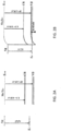
- FIG. 1A illustrates a top plan view of a Bi 2 Te 3 nanoparticle having platelet morphology according to some embodiments described herein.
- the Bi 2 Te 3 nanoparticle 10 comprises a front face 11 and an opposing back face (not shown). Sidewalls 12 extend between the front face 12 and back face.
- FIG. 1B illustrates metallic nanoparticle 13 nucleation and growth on sidewalls 12 of the Bi 2 Te 3 nanoparticle 10.
- FIG. 2A illustrates the band diagram of a Sb 2 Te 3 nanoparticle prior to nucleation and growth of silver nanoparticles along one or more sidewalls.
- the work function of silver is also illustrated in FIG. 2A .
- the initial Fermi level of Ag is located above the intrinsic Sb 2 Te 3 .
- the presence of Ag nanoparticles pins the effective Fermi level of the present nanocomposites around the work function of silver due to the large carrier density in the metallic layer. As can be seen in FIG.
- the blend band gap between the host Sb 2 Te 3 semiconductor and metallic Ag nanoparticles forms a Schottky barrier, which is believed to be much better than Ohmic contact.
- the potential barrier height ( ⁇ 150 meV) is around the theoretical optimized height of 100 meV. Therefore, interfaces in Ag-Sb 2 Te 3 nanoplates induce energy-dependent carrier scattering by introducing a Schottky barrier to filter carriers with low energy, i.e. the carrier filtering technique prevents the transport of the lower-energy carriers, which results in an increase in the moment of the differential conductivity about the Fermi level.
- the metallic nanoparticles bridge spacing between adjacent semiconductor nanoparticles to provide composite nanoparticle assemblies.
- a metal nanoparticle for example extends from a sidewall of a first semiconductor nanoparticle to bond to a sidewall of a second adjacent semiconductor nanoparticle.
- nanocomposite assemblies are formed as illustrated in FIG. 3 . Spacing between the platelet Sb 2 Te 3 nanoparticles 10 is filled with metallic nanoparticles 13 bound to sidewalls of the Sb 2 Te 3 nanoparticles. Schottky barriers can be established at metal-semiconductor interfaces along the sidewalls permitting filtering of low energy carriers as described herein. Filtering of the low energy carriers can enhance electrical conductivity of the composite nanoparticle assembly.
- a nanocomposite assembly has an electrical conductivity of at least 1 ⁇ 10 4 S/m or at least 1 ⁇ 10 5 S/m. Additionally, the metal nanoparticles can enhance phonon scattering, thereby lowering thermal conductivity of the nanocomposite assembly. Seebeck coefficient of the semiconductor nanoparticles can also be improved by the presence of the metal nanoparticles. In some embodiments, a nanocomposite assembly has a room temperature Seebeck coefficient of at least 140 ⁇ V/K. The foregoing enhancements also increase the power factor of composite nanoparticle assemblies described herein. In some embodiments, a nanoparticle assembly has a power factor greater than 600 ⁇ W/mK 2 or a power factor greater than 1000 ⁇ W/mK 2 .
- Composite nanoparticle assemblies can be formed into thin flexible films for various thermoelectric applications.
- Composite nanoparticle assemblies in some embodiments, are stacked to provide thin film architectures.
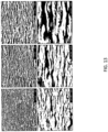
- Cross-sectional structure of the stacked composite assemblies can include porosity or open spaces between composite nanoparticle assemblies. Such porosity and/or open spaces are illustrated in FIG. 13.
- FIG. 13 provides scanning electron microscopy (SEM) images of pellet based Bi 2 Te 3 nanoplates after Ag decoration at different magnifications according to some embodiments.
- a method of enhancing chalcogenide thermoelectric performance comprises providing chalcogenide nanoparticles comprising front and back faces and sidewalls extending between the front and back faces. At least one of electrical conductivity and Seebeck coefficient of the chalcogenide nanoparticles is increased via nucleation of metallic nanoparticles on the sidewalls, wherein the metallic nanoparticles bridge spacing between the chalcogenide nanoparticles. Moreover, thermal conductivity of the chalcogenide nanoparticles can be decreased the metal nanoparticles bridging spacing between adjacent nanoparticles.
- V-VI Sb 2 Te 3 was selected because of its state-of-the-art performance that exhibits the highest ZT near 50 °C.
- Silver was chosen as the metallic nanoparticle phase due to its low work function (4.26-4.9 eV) needed for efficient carrier injection into the Sb 2 Te 3 conduction band.
- work function (4.26-4.9 eV) needed for efficient carrier injection into the Sb 2 Te 3 conduction band.
- Ag can be reduced from AgNO 3 in ethyl alcohol (EG) at room temperature.
- EG ethyl alcohol
- ethylene glycol (EG) solution containing mixed antimony trichloride (SbCl 3 , 6 mmol), tellurium dioxide (TeO 2 , 9 mmol), sodium hydroxide (NaOH, 1.5 g), and polyvinylpyrrolidone (PVP, M s ⁇ 40000 g/mol, 0.8 g) are heated to 120 °C.
- 10 ml hydrazine hydrate (N 2 H 4 ) was injected (with injection rate 2.5 ml/min), and the solution were maintained at 130 °C for 3 hours. After which, the mixture are heated at 155 °C under reflux for another 15 hours.
- the precipitates were collected by centrifugation, washed using ethanol for at least three times. Finally, a simple and efficacious vacuum filtration process is adopted to fabricate the Sb 2 Te 3 -based thin film using water as solution.
- the Sb 2 Te 3 -based nanocomposites were dispersed in water via homogenization and sonication, subsequently, the resulting aqueous suspension was vacuum-filtered through a poly(vinylidene difluoride) (PVDF) filter (0.1 ⁇ m pore size) to form a silver gray film (shiny metallic appearance) on the filter surface.
- PVDF poly(vinylidene difluoride)
- the fabricated thin film can finally be transform to different substrates (like Silicon or PET) for different applications.
- the active Sb 2 Te 3 edges with exposed Te dangling bonds are believed to act as heterogeneous nucleation sites, first reacting with Ag + and then facilitating the growth of Ag nanoparticles with the help of a reducing agent (EG).
- EG reducing agent
- No dissociate Ag nanoparticles were found in the solution (dynamically unstable) or on the surface of the Sb 2 Te 3 nanoplates, suggesting that laterally selective growth is more preferable (calculated as -0.113 eV/ ⁇ 2 compared with -0.037 eV/ ⁇ 2 that growth on the face).
- the strain in the crystal lattice is beneficial to the decrease of the lattice thermal conductivity contribution by strain field scattering.
- Ag-decorated Sb 2 Te 3 nanocomposites possess significantly higher electrical conductivities around 3.5 ⁇ 10 4 S/m, which is eight times larger than that of the Sb 2 Te 3 based thin film and even comparable to the bulk Sb 2 Te 3 pellet.
- the Seebeck coefficient also increases from 84 to 103 ⁇ V/K at 300 K (>20%) after nanoengineering.
- Ag-decorated Sb 2 Te 3 nanocomposite based films give a power factor of 371 ⁇ W/mK 2 , which is much higher than our previous Bi 2 Se 3 -based thin films and other Sb 2 Te 3 -based films.
- the electrical conductivity and Seebeck coefficient of the present films exhibited high stability against the bending test, demonstrating no apparent change in performance upon repeated bending for up to 500 cycles under bending radius 2 mm.
- the boost in performance results from the simultaneously enhanced electrical conductivity and Seebeck coefficients.
- the enhanced electrical conductivity is explained by an efficient injection of carriers from the metallic Ag to the conduction band of the Sb 2 Te 3 semiconductor.
- a room temperature Hall measurement was performed, which reveals a remarkable increase in carrier concentration from 1.4 ⁇ 10 19 cm -3 to 9.9 ⁇ 10 19 cm -3 with a slight decrease of mobility from 25 to 22 cm 2 V -1 S -1 , as can be seen in Table 1.
- FIGS 2A and 2B The band alignment between Sb 2 Te 3 and Ag nanoparticles is shown in FIGS 2A and 2B .
- the detailed electrical information of Sb 2 Te 3 and the work function of silver nanoparticles ( ⁇ 4.3 eV) are taken from experiments. The assumption of bulk is reasonable since the thickness of the bottom layer of Sb 2 Te 3 is around 10 nm, which corresponds to 10 QL.
- the Fermi level ( E F ) is positioned near the top of valence band maximum with a small gap at the ⁇ - point according to previous study. Before contact, the initial Fermi level of Ag is located above the intrinsic Sb 2 Te 3 .
- the presence of Ag nanoparticles pins the effective Fermi level of the present nanocomposites around the work function of silver due to the large carrier density in the metallic layer.
- the blend band gap between the host Sb 2 Te 3 semiconductor and metallic Ag nanoparticles forms a Schottky barrier, which is believed to be much better than Ohmic contact.
- the potential barrier height ( ⁇ 150 meV) is around the theoretical optimized height of 100 meV. Therefore, interfaces in Ag-Sb 2 Te 3 nanoplates induce energy-dependent carrier scattering by introducing a Schottky barrier to filter carriers with low energy, i.e. the carrier filtering technique described above is preventing the transport of the lower-energy carriers, which results in an increase in the moment of the differential conductivity about the Fermi level.
- PVP polyvinylpyrrolidone
- ethylene glycol (EG) solution containing mixed antimony trichloride (SbCl 3 , 6 mmol), tellurium dioxide (TeO 2 , 9 mmol), sodium hydroxide (NaOH, 1.5 g), and polyvinylpyrrolidone (PVP, M s ⁇ 40000 g/mol, 0.8 g) are heated to 120 °C.
- 10 ml hydrazine hydrate (N 2 H 4 ) was injected (with injection rate 2.5 ml/min), and the solution were maintained at 130 °C for 3 hours. After which, the mixture are heated at 155 °C under reflux for another 15 hours.
- the precipitates were collected by centrifugation, washed using ethanol for at least three times to remove any unreacted chemicals and ethylene glycol from the surface.
- the dried nanocomposites were loaded into a graphite die and compacted into pellets ( ⁇ 10 mm ⁇ ⁇ 1.5 mm).
- the process was carried out in Ar atmosphere, using a custom-made hot press to simultaneously apply a pressure of 70 MPa and a temperature of 370-380 °C during 30 min.
- the heat was provided by an induction coil operated at 30-80 KHz and it was applied directly to a graphite die acting as a susceptor.
- Fast heating ramps of 20 °C s -1 are reached by this method with a 25 kW induction heater. All the pellets were mechanically robust enough to endure polishing.
- XRD X-ray diffraction
- SAED selected area electron diffraction
- SAEDX selected area electron diffraction
- EDX selected area electron diffraction
- AFM Atomic Force Microscope
- XPS X-ray photoelectron spectroscopy
- the morphology of the Bi 2 Te 3 /Sb 2 Te 3 nanoplates and Ag-decorated Bi 2 Te 3 /Sb 2 Te 3 nanocomposites were measured by the Scanning Electron Microscope (SEM, JEOL, JSM-6330F).
- SEM Scanning Electron Microscope
- Thermogravimetric (TG) and differential scanning calorimetric (DSC) were measured with a TG-DTA/DSC thermal analyzer (Netzsch, Germany) with a heating rate of 10°C/min in flowing N 2 gas.
- thermoelectric properties Seebeck coefficients were measured using a static DC method, and electrical resistivity data was obtained by a standard four-probe method. Both the Seebeck coefficient and the electrical resistivity were measured simultaneously in a LSR-3 LINSEIS system in the temperature range between room temperature and 600 K, under helium atmosphere. At each temperature at least three consecutive measurements were performed to get rid of the minor variations. Taking into account the system accuracy and the measurement precision, we estimate an error of ca. 4 % in the measurement of the electrical conductivity and Seebeck coefficient.
- the thermal diffusivity coefficient (D) was measured between 300-600 K by the A XFA 600 Xenon Flash apparatus from Linseis.
- the heat capacity (C p ) was measured using differential scanning calorimetry (DSC, Netzsch DSC-404C) with an associated error of ca. 2%.
- the density ( ⁇ ) was determined using the dimensions and mass of the sample and then reconfirmed using the Archimedes method.
- the Hall coefficient (R H ) was determined using a physical properties measurement system (PPMS-9T) under a magnetic field of 2T and electrical current.
- the Hall mobility ⁇ R H ⁇ , where ⁇ is the electrical resistivity.
- FIG. 10A illustrates temperature dependent electrical properties of Ag-decorated Bi 2 Te 3 pellets with different Ag concentrations.
- FIG. 10B illustrates temperature dependent thermal transport properties of Ag-decorated Bi 2 Te 3 pellets with different Ag concentrations.
- FIG. 11 illustrates temperature dependent electrical and thermal transport properties of Cu-decorated Bi 2 Te 3 pellets with different Cu concentrations.
- concentrations of Ag or Cu on Bi 2 Te 3 nanoplates can be fine-adjusted by AgNO 3 or CuI/CuCl precursors.
- metal-free Bi 2 Te 3 exhibits a relatively low electrical conductivity ( ⁇ ) around 1.0 ⁇ 10 4 S/m at room temperature (RT).
- ⁇ electrical conductivity
- RT room temperature
- One reason for this low value compared with Bi 2 Te 3 ingot is the thermal degradation residue from the capping PVP ligand.
- the ⁇ gradually increases with the self-assembled metallic nanoparticles.
- nanocomposites with 15 at% Ag exhibit a significantly increased ⁇ up to 2.8 ⁇ 10 4 S/m at RT, which is nearly three times compared with pure Bi 2 Te 3 .
- With temperature all the nanocomposites show a nondegenerate semiconductor behavior, i.e. the ⁇ increases slightly with the temperature over the studied measurement range 300-550 K. This is in agreement with the nanostructured Bi 2 Te 3 observed previously. This behavior can be attributed to the thermal excitation carrier concentrations (n) across the band gap and the increased extrinsic n with the increasing temperature.
- Energy filtering effect is normally qualitatively to explain the increased S by based on simple band gap alignment.
- introduced chemical bonding at the interface plays important roles in determining the electrical band structures and the Schottky-barrier height (SHB), thus detailed first principles calculations involved in a more accurate treatment of the interface dipole is necessary.
- DFT calculations were carried out in order to uncover the mechanism behind the decoupled phenomenon.
- the introduced metal nanoparticles are capable to inject charge carriers and facilitate promising efficient charge transport across neighboring nanoplates and the whole pellet.
- the phonon scattering in nanostructured materials is strongly dependent on the numerous interfaces between the nanostructures, the self-assembled metal nanoparticles might also assist in blocking phonon propagation that transport large fraction of heat.
- This interface scattering in nanostructures originated from the enhanced phonon boundary scattering and the low energy electrons filtering, with which the compression of ⁇ L is expected.
- Nanoscale precipitates and mesoscale grains acting as multi-wavelength phonon scattering centers were indeed preserved. Based on the Rayleigh scattering regime, the scattering cross section is defined as ⁇ ⁇ b 6 / ⁇ 4 , where b and ⁇ are the size of the scattering particles and phonon wavelength, respectively.
- the size of the Ag nanoparticles is around 40 nm, which is sufficiently large enough to create a scattering regime that does not overlap Rayleigh scattering on the atomic scale ( ⁇ 1 ⁇ ). Therefore, both Ag/Cu nanoparticles and the second phase Ag 2 Te/Cu 2 Te are thought to assist in blocking propagation of phonons with mid to long wavelengths that transport a large fraction of heat; thus, significantly reducing ⁇ L in nanocomposites is achieved.
- ⁇ L shows a continuous decrease with Ag concentrations, for Ag-free Bi 2 Te 3 and Ag-decorated Bi 2 Te 3 at RT, respectively. These values lie within the minimum range of lattice thermal conductivity (0.1-0.2 W ⁇ m -1 ⁇ K -1 ) defined by Slack.
- thermoelectrical ZT is increased from 0.1 to 0.3 via the present heterojunction architectures for Ag-decorated Bi 2 Te 3 .
- the ZT is optimized to 0.3 at RT.
Landscapes
- Chemical & Material Sciences (AREA)
- Organic Chemistry (AREA)
- Inorganic Chemistry (AREA)
- Engineering & Computer Science (AREA)
- Manufacturing & Machinery (AREA)
- Materials Engineering (AREA)
- Powder Metallurgy (AREA)
Description
- This invention was made with government support under Grant No. FA9550-16-1-0328 awarded by the U.S. Air Force Office of Scientific Research and Grant No. 1123-SC-01-R0 NASA #NNX16CJ30P awarded by NASA/Streamline. The government has certain rights in the invention.
- The present application claims priority pursuant to Patent Cooperation Treaty
Article 8 and 35 U.S.C. § 119(e) toUnited States Provisional Patent Application Serial Number 62/459,978 filed February 16, 2017 - The present invention relates to composite nanoparticles and associated assemblies and, in particular, to composite nanoparticles and assemblies exhibiting enhanced thermoelectric properties.
- Solid-state energy conversion utilizing thermoelectric (TE) materials has attracted increasing interest due to their unparalleled properties to convert waste heat to electric energy. The efficiency of TE materials is expressed by a dimensionless figure of merit ZT, which is governed by electrical conductivity (σ), Seebeck coefficient (S), and thermal conductivity (κ) that mainly includes the lattice thermal conductivity κL and carrier thermal conductivity κc (κL >>κc ). An ideal efficient TE material necessarily to possesses high σ and a low κ. Unfortunately, for most TE systems, these three parameters are interdependent, thus maximizing one normally counteracts or reduces the other two. This has ultimately prevented the widespread application of TE materials as noise-free power generators or scalable solid-state Peltier coolers.
US 2007/0269991 A1 discloses a semiconductor nanocrystal-metal complex and method of preparing the same. Furthermore, the publication KYU-HYOUNG LEE ET AL: "Enhancement of Thermoelectric Figure of Merit for Bi0.5Sb1.5Te3 Metal Nanoparticle Decoration",JOURNAL OF ELECTRONIC MATERIALS, SPRINGER US, BOSTON, vol. 41, no. 6, 10 February 2012 (2012-02-10), pages 1165-1169, XP035057886,ISSN: 1543-186X, DOI: 10.1007/S11664-012-1913-0 discloses a chalcogenide nanocomposite with nanoscale metal particles. - Composite nanoparticle compositions and associated nanoparticle assemblies are described herein which, in some embodiments, exhibit enhancements to one or more thermoelectric properties including increases in electrical conductivity and/or Seebeck coefficient and/or decreases in thermal conductivity. In one aspect, a composite nanoparticle composition comprises a semiconductor nanoparticle including a front face and a back face and sidewalls extending between the front and back faces. Metallic nanoparticles nucleated and grown on at least one of the sidewalls, are bonded to at least one of the sidewalls establishing a metal-semiconductor junction, wherein the composite nanoparticle has a platelet, a pyramidal, or a bi-pyramidal morphology. In some embodiments, the metallic nanoparticles are bonded to a plurality of the semiconductor nanoparticle sidewalls establishing multiple metal-semiconductor junctions.
- In another aspect, composite nanoparticle assemblies are described herein. Briefly, a composite nanoparticle assembly comprises semiconductor nanoparticles comprising front and back faces and sidewalls extending between the front and back faces, wherein spacing between the semiconductor nanoparticles is bridged by metallic nanoparticles bonded to the sidewalls of the semiconductor nanoparticles. As described further herein, the bridging metallic nanoparticles establish metal-semiconductor junctions with sidewalls of the semiconductor nanoparticles.
- In a further aspect, methods of enhancing metal chalcogenide thermoelectric performance are provided. In some embodiments, a method of enhancing metal chalcogenide thermoelectric performance comprises providing metal chalcogenide nanoparticles comprising front and back faces and sidewalls extending between the front and back faces, said metal chalcogenide nanoparticles having a platelet, a pyramidal, or a bi-pyramidal morphology.
- At least one of electrical conductivity and Seebeck coefficient of the chalcogenide nanoparticles is increased via nucleation and growth of metallic nanoparticles on the sidewalls, wherein the metallic nanoparticles bridge spacing between the chalcogenide nanoparticles. Moreover, thermal conductivity of the chalcogenide nanoparticles can be decreased by the metal nanoparticles bridging spacing between adjacent nanoparticles.
- These and other embodiments are described in greater detail in the following detailed description.
-
-
FIG. 1A illustrates a top plan view of a platelet semiconductor nanoparticle according to some embodiments. -
FIG. 1B illustrate metallic nanoparticles bonded to sidewalls of the platelet semiconductor nanoparticle according to some embodiments. -
FIG. 2A illustrate band structure of Sb2Te3 nanoparticle and Ag metal according to some embodiments. -
FIG. 2B illustrate band structure of an Ag nanoparticle- Sb2Te3 nanoparticle interface according to some embodiments. -
FIG. 3 illustrates a composite nanoparticle assembly according to some embodiments. -
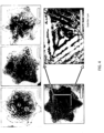
FIG. 4 illustrates transmission electron microscopy (TEM) images of composite nanoparticles according to some embodiments. -
FIG. 5 illustrates a freestanding composite nanoparticle assembly film according to some embodiments. -
FIG. 6 illustrates X-ray diffraction measurements of Sb2Te3 nanoplates and Sb2Te3 nanoplates having silver nanoparticles bound to sidewalls according to some embodiments. -
FIG. 7 illustrates a high resolution TEM image of a composite nanoparticle according to some embodiments. -
FIG. 8 illustrates XPS of Sb2Te3 and Ag-decorated Sb2Te3 conducted to study the chemical environment of each element. -
FIG. 9 illustrates TGA and DSC analyses of Sb2Te3 nanoplates and Ag-decorated Sb2Te3 nanoplates according to some embodiments. -
FIG. 10A illustrates temperature dependent electrical properties of Ag-decorated Bi2Te3 pellets with different Ag concentrations. -
FIG. 10B illustrates temperature dependent thermal transport properties of Ag-decorated Bi2Te3 pellets with different Ag concentrations. -
FIG. 11 illustrates temperature dependent electrical and thermal transport properties of Cu-decorated Bi2Te3 pellets with different Cu concentrations. -
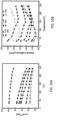
FIG. 12 summarizes the room temperature (RT) performance for both Cu- and Ag-decorated Bi2Te3. -
FIG. 13 provides scanning electron microscopy images of pellet based Bi2Te3 nanoplates after Ag decoration at different magnifications according to some embodiments. -
FIG. 14 illustrates pyramidal or bi-pyramidal morphology of semiconductor nanoparticles according to some embodiments described herein. - Embodiments described herein can be understood more readily by reference to the following detailed description and examples and their previous and following descriptions.
- In one aspect, a composite nanoparticle composition comprises a semiconductor nanoparticle including a front face and a back face and sidewalls extending between the front and back faces. Metallic nanoparticles are bonded to at least one of the sidewalls establishing a metal-semiconductor junction. In some embodiments, the metallic nanoparticles are bonded to a plurality of the semiconductor nanoparticle sidewalls establishing multiple metal-semiconductor junctions. The semiconductor nanoparticle can comprise any semiconductor not inconsistent with the thermoelectric principles and electronic structures described herein. Suitable semiconductor nanoparticles can include various chalcogenides, such as metal sulfides, metal selenides and/or metal tellurides. Moreover, semiconductor nanoparticles can be p-type or n-type. For example, semiconductor nanoparticles can comprise molybdenum sulfide (MoS2), antimony telluride (Sb2Te3) or bismuth telluride (Bi2Te3). Additionally, semiconductor nanoparticles of the composite composition provide sidewalls for bonding and nucleation of the metallic nanoparticles. In some embodiments, semiconductor nanoparticles have two-dimensional (2D) morphology. A semiconductor nanoparticle, for example, can be a platelet wherein the metal nanoparticles are bonded to one or more sidewalls of the platelet. Semiconductor nanoparticles, in some embodiments, exhibit a pyramidal or bi-pyramidal structure. Non-limiting examples of pyramidal or bi-pyramidal structures are illustrated in
FIG. 14 . - Metallic nanoparticles bonded to one or more sidewalls of a semiconductor nanoparticle can comprise any metal not inconsistent with the thermoelectric principles and electronic structures described herein. Suitable metals include various transition metals, such as metals selected from Groups IVA-VIIIA and Group IB of the Periodic Table. In some embodiments, the metallic nanoparticles are formed of noble metal(s). The metal nanoparticles can nucleate and self-assemble on sidewall surfaces of the semiconductor nanoparticles. In being bonded to the semiconductor nanoparticle sidewall, an interfacial transition region can be established between the metal nanoparticle and semiconductor. In some embodiments, the interfacial transition region comprises metal atoms chemically bonded to atoms of the semiconductor nanoparticle. In one example, silver nanoparticles are bonded to sidewalls of a Sb2Te3 nanoparticle, wherein an interfacial transition region comprises Sb2Te3-Ag2Te-Ag. Metal nanoparticles bonded to semiconductor sidewalls can have any size not inconsistent with the objectives of the present invention. In some embodiments, metal nanoparticle size is governed by spacing between the semiconductor nanoparticles in a composite assembly. As described further herein, the metal nanoparticles can bridge spacing between adjacent semiconductor nanoparticles, binding to sidewalls of the semiconductor nanoparticles. In such embodiments, composite nanoparticle assemblies can be formed.
-
FIG. 1A illustrates a top plan view of a Bi2Te3 nanoparticle having platelet morphology according to some embodiments described herein. The Bi2Te3 nanoparticle 10 comprises afront face 11 and an opposing back face (not shown).Sidewalls 12 extend between thefront face 12 and back face.FIG. 1B illustratesmetallic nanoparticle 13 nucleation and growth on sidewalls 12 of the Bi2Te3 nanoparticle 10. - Bonding and growth of metallic nanoparticles on sidewalls of the semiconductor establishes a metal-semiconductor junction. In some embodiments, a Schottky barrier is formed at the metal semiconductor junction.
FIG. 2A illustrates the band diagram of a Sb2Te3 nanoparticle prior to nucleation and growth of silver nanoparticles along one or more sidewalls. The work function of silver is also illustrated inFIG. 2A . Before contact, the initial Fermi level of Ag is located above the intrinsic Sb2Te3. After nucleation and growth, the presence of Ag nanoparticles pins the effective Fermi level of the present nanocomposites around the work function of silver due to the large carrier density in the metallic layer. As can be seen inFIG. 2B , the blend band gap between the host Sb2Te3 semiconductor and metallic Ag nanoparticles forms a Schottky barrier, which is believed to be much better than Ohmic contact. Moreover, the potential barrier height (~150 meV) is around the theoretical optimized height of 100 meV. Therefore, interfaces in Ag-Sb2Te3 nanoplates induce energy-dependent carrier scattering by introducing a Schottky barrier to filter carriers with low energy, i.e. the carrier filtering technique prevents the transport of the lower-energy carriers, which results in an increase in the moment of the differential conductivity about the Fermi level. - The metallic nanoparticles bridge spacing between adjacent semiconductor nanoparticles to provide composite nanoparticle assemblies. A metal nanoparticle, for example extends from a sidewall of a first semiconductor nanoparticle to bond to a sidewall of a second adjacent semiconductor nanoparticle. When occurring over multiple sidewalls, nanocomposite assemblies are formed as illustrated in
FIG. 3 . Spacing between the platelet Sb2Te3 nanoparticles 10 is filled withmetallic nanoparticles 13 bound to sidewalls of the Sb2Te3 nanoparticles. Schottky barriers can be established at metal-semiconductor interfaces along the sidewalls permitting filtering of low energy carriers as described herein. Filtering of the low energy carriers can enhance electrical conductivity of the composite nanoparticle assembly. In some embodiments, a nanocomposite assembly has an electrical conductivity of at least 1 × 10⁴ S/m or at least 1 × 10⁵ S/m. Additionally, the metal nanoparticles can enhance phonon scattering, thereby lowering thermal conductivity of the nanocomposite assembly. Seebeck coefficient of the semiconductor nanoparticles can also be improved by the presence of the metal nanoparticles. In some embodiments, a nanocomposite assembly has a room temperature Seebeck coefficient of at least 140 µV/K. The foregoing enhancements also increase the power factor of composite nanoparticle assemblies described herein. In some embodiments, a nanoparticle assembly has a power factor greater than 600 µW/mK2 or a power factor greater than 1000 µW/mK2. - Composite nanoparticle assemblies can be formed into thin flexible films for various thermoelectric applications. Composite nanoparticle assemblies, in some embodiments, are stacked to provide thin film architectures. Cross-sectional structure of the stacked composite assemblies can include porosity or open spaces between composite nanoparticle assemblies. Such porosity and/or open spaces are illustrated in
FIG. 13. FIG. 13 provides scanning electron microscopy (SEM) images of pellet based Bi2Te3 nanoplates after Ag decoration at different magnifications according to some embodiments. - In a further aspect, methods of enhancing chalcogenide thermoelectric performance are provided. In some embodiments, a method of enhancing chalcogenide thermoelectric performance comprises providing chalcogenide nanoparticles comprising front and back faces and sidewalls extending between the front and back faces. At least one of electrical conductivity and Seebeck coefficient of the chalcogenide nanoparticles is increased via nucleation of metallic nanoparticles on the sidewalls, wherein the metallic nanoparticles bridge spacing between the chalcogenide nanoparticles. Moreover, thermal conductivity of the chalcogenide nanoparticles can be decreased the metal nanoparticles bridging spacing between adjacent nanoparticles.
- These and other embodiments are further illustrated in the following non-limiting examples.
- V-VI Sb2Te3 was selected because of its state-of-the-art performance that exhibits the highest ZT near 50 °C. Silver was chosen as the metallic nanoparticle phase due to its low work function (4.26-4.9 eV) needed for efficient carrier injection into the Sb2Te3 conduction band. In detail, using the ultrathin/active Sb2Te3 edge as the nucleation sites, Ag can be reduced from AgNO3 in ethyl alcohol (EG) at room temperature. As a result, Ag nanoparticles with diameters around 40 nm were found to grow uniformly at the edge of the Sb2Te3 nanoplates.
- Actually, a slight layer of second phase (n-type Ag2Te) was also introduced in this process. These interfaces among Sb2Te3-Ag2Te-Ag act as a low-energy carrier and phonon scattering center, which facilitates the enhancement of the Seebeck coefficient (from 84 to 103 µV/K) and the suppression of thermal conductivity. Meanwhile, the electrical conductivity was also improved from 4.4×10³ to 3.5×10⁴ S/m due to the increased carrier concentration with a slight decrease of carrier mobility. This simultaneous enhancement of electrical conductivity and Seebeck coefficients demonstrates that these self-assembled Ag nanoparticles are able to inject charge carriers and facilitate charge transport between Sb2Te3 nanoplates; at the same time, the generated the energy barrier among Ag nanoparticles, the introduced Ag2Te second phase and Sb2Te3 nanoplatelets also assist in blocking charge carriers with lower energy, facilitate the decoupling of the Seebeck coefficient and electrical conductivity.
- In a typical synthesis, 70 ml ethylene glycol (EG) solution containing mixed antimony trichloride (SbCl3, 6 mmol), tellurium dioxide (TeO2, 9 mmol), sodium hydroxide (NaOH, 1.5 g), and polyvinylpyrrolidone (PVP, Ms ≈ 40000 g/mol, 0.8 g) are heated to 120 °C. 10 ml hydrazine hydrate (N2H4) was injected (with injection rate 2.5 ml/min), and the solution were maintained at 130 °C for 3 hours. After which, the mixture are heated at 155 °C under reflux for another 15 hours. The precipitates were collected by centrifugation, washed using ethanol for at least three times. Finally, a simple and efficacious vacuum filtration process is adopted to fabricate the Sb2Te3-based thin film using water as solution. In details, the Sb2Te3-based nanocomposites were dispersed in water via homogenization and sonication, subsequently, the resulting aqueous suspension was vacuum-filtered through a poly(vinylidene difluoride) (PVDF) filter (0.1 µm pore size) to form a silver gray film (shiny metallic appearance) on the filter surface. The fabricated thin film can finally be transform to different substrates (like Silicon or PET) for different applications. For the fabrication of Ag-decorated Sb2Te3 nanocomposites, 1 mmol as-fabricated Sb2Te3 was dispersed in 70 mL EG, and proper amount of AgNO3 was added with gently and stirred over night at room temperature. The precipitates were collected by centrifugation, washed using ethanol for at least three times. Finally, the vacuum filtration process is adopted to fabricate the flexible thin film based on Ag-decorated Sb2Te3 using water as solution. Ag nanoparticles with high uniformity were observed to embed regularly around the edges of the Sb2Te3 nanoplates, as evidenced by TEM images of
FIG. 4 . Freestanding flexible Ag-decorated Sb2Te3 thin film is illustrated inFIG. 5 . - The active Sb2Te3 edges with exposed Te dangling bonds are believed to act as heterogeneous nucleation sites, first reacting with Ag+ and then facilitating the growth of Ag nanoparticles with the help of a reducing agent (EG). No dissociate Ag nanoparticles were found in the solution (dynamically unstable) or on the surface of the Sb2Te3 nanoplates, suggesting that laterally selective growth is more preferable (calculated as -0.113 eV/Å2 compared with -0.037 eV/Å2 that growth on the face). The strain in the crystal lattice is beneficial to the decrease of the lattice thermal conductivity contribution by strain field scattering. By using XRD measurement, a slight amount of Ag2Te was also found beyond Ag (peaks 29.8° and 31° that corresponds to the main peak of monoclinic phase Ag2Te), which likely occurs in the beginning of nucleation as illustrated in
FIG. 6 . That is in agreement with the slight layer (~3 nm) of second phase (n-type Ag2Te, P2/n, and PDF No. 34-0142) observed by HRTEM inFIG. 7 , implying the uniformly generated Sb2Te3-Ag2Te-Ag interfaces. Here, by using self-assembled nanoengineering, a uniform p-n junction was generated around each Sb2Te3 nanoplate, which might be one of the main reasons this unique heterojunction has extremely high electrical conductivity while maintaining a decent Seebeck coefficient. XPS of Sb2Te3 and Ag-decorated Sb2Te3 have been conducted to study the chemical environment of each element as provided inFIG. 8 . The 3d 3/2 and 3d 5/2 peaks of Ag are located at 373.40 and 367.8 eV, respectively. Interestingly, a slight shoulder peak appears in the Sb2Te3 sample due to the oxidation states of Te compared to the sharp peak of the Ag-decorated Sb2Te3 sample. This means the oxidative stability of the nanocomposites is strengthened after Ag-decoration. TGA and DSC analyses of Sb2Te3 nanoplates and Ag-decorated Sb2Te3 nanocomposites are also given inFIG. 9 . - Ag-decorated Sb2Te3 nanocomposites possess significantly higher electrical conductivities around 3.5×10⁴ S/m, which is eight times larger than that of the Sb2Te3 based thin film and even comparable to the bulk Sb2Te3 pellet. At the same time, the Seebeck coefficient also increases from 84 to 103 µV/K at 300 K (>20%) after nanoengineering. As a result, with the enhanced electrical conductivity and improved Seebeck coefficient, Ag-decorated Sb2Te3 nanocomposite based films give a power factor of 371 µW/mK2, which is much higher than our previous Bi2Se3-based thin films and other Sb2Te3-based films. The electrical conductivity and Seebeck coefficient of the present films exhibited high stability against the bending test, demonstrating no apparent change in performance upon repeated bending for up to 500 cycles under bending
radius 2 mm. The boost in performance results from the simultaneously enhanced electrical conductivity and Seebeck coefficients. Here, the enhanced electrical conductivity is explained by an efficient injection of carriers from the metallic Ag to the conduction band of the Sb2Te3 semiconductor. To clarify the above mechanism, a room temperature Hall measurement was performed, which reveals a remarkable increase in carrier concentration from 1.4×1019 cm-3 to 9.9×1019 cm-3 with a slight decrease of mobility from 25 to 22 cm2V-1S-1, as can be seen in Table 1. This is also in agreement with the estimated results from the increase of equivalent conductivity (in unit of the relaxation time τ) for Ag-decorated Sb2Te3 nanocomposites compared with Ag-free Sb2Te3 based on first-principles calculations.Table 1. Carrier concentrations and carrier mobilities Sb2Te3 based or Sb2Te3 related nanostructures based thin films at 300 K. Materials Carrier Concentration (×1019 cm-3) Mobility (cm2V-1S-1) Seebeck (µV/K) Electrical Conductivity (S/m) Power Factor (µW/mK2) Sb2Te3 1.67 28 116 7.3×10³ 96 Pt-Sb2Te3 Sb2Te3 2.46 11.4 152 4.4×10³ 102 Annealed 420 K 1.5 14 124 3.9×10³ 60 Annealed 470 K 1.7 26 114 7.0×10³ 91 AgxTey-Sb2Te3 Ag31Sb19Te50 8.9 4.1 135 5.6×10³ 102 AgxTey-Sb2Te3 Ag34Sb18Te48 11 5.8 93 1.07×10⁴ 93 Sb2Te3 a) 1.4 25 84 5.6×10³ 40 Ag-Sb2Te3 a) 9.9 22 103 3.5×10⁴ 371 a) The results in the present work without annealing. - A beneficial energy barrier is introduced between the metallic nanoparticles and semiconductor nanoplates to maintain a decent Seebeck coefficient. The band alignment between Sb2Te3 and Ag nanoparticles is shown in
FIGS 2A and 2B . The detailed electrical information of Sb2Te3 and the work function of silver nanoparticles (~4.3 eV) are taken from experiments. The assumption of bulk is reasonable since the thickness of the bottom layer of Sb2Te3 is around 10 nm, which corresponds to 10 QL. The Fermi level (E F) is positioned near the top of valence band maximum with a small gap at the Γ-point according to previous study. Before contact, the initial Fermi level of Ag is located above the intrinsic Sb2Te3. After Ag decoration, the presence of Ag nanoparticles pins the effective Fermi level of the present nanocomposites around the work function of silver due to the large carrier density in the metallic layer. As can be seen, the blend band gap between the host Sb2Te3 semiconductor and metallic Ag nanoparticles forms a Schottky barrier, which is believed to be much better than Ohmic contact. Moreover, the potential barrier height (~150 meV) is around the theoretical optimized height of 100 meV. Therefore, interfaces in Ag-Sb2Te3 nanoplates induce energy-dependent carrier scattering by introducing a Schottky barrier to filter carriers with low energy, i.e. the carrier filtering technique described above is preventing the transport of the lower-energy carriers, which results in an increase in the moment of the differential conductivity about the Fermi level. - In summary, increasing the electrical conductivity while maintaining or even enhancing the Seebeck coefficient by chopping the distribution cold carriers is achieved with the introduced self-assembled heterojunction architectures, leading to a dramatically increased power factor for the present flexible thermoelectric fabrics. Further, to roughtly estimate the thermal conductivity of the present system, we made samples with thickness aournd 100 µm. The room temperature thermal conductivity of Ag-decorated Sb2Te3 nanocomposites was determined around 0.44 W/m·K, which gives a ZT of 0.23.
- In order to fabricate Bi2Te3 nanoplates, 2 mmol Bi(NO3)3 and 3 mmol Na2TeO3 was dissolved in 70 mL ethylene glycol, 1.5 g NaOH was added with vigorous stirring, and followed by 0.5 g polyvinylpyrrolidone (PVP, Ms=40000 g/mol) and refluxing the mixture solution at 185 °C over night. After the mixture cool down to room temperature, Acetone was used to precipitate the fabricated Bi2Te3 nanoplates and then re-dissolve by Ethanol. This process was repeated three times to remove any unreacted chemicals and ethylene glycol from the surface.
- In a typical synthesis, 70 ml ethylene glycol (EG) solution containing mixed antimony trichloride (SbCl3, 6 mmol), tellurium dioxide (TeO2, 9 mmol), sodium hydroxide (NaOH, 1.5 g), and polyvinylpyrrolidone (PVP, Ms ≈ 40000 g/mol, 0.8 g) are heated to 120 °C. 10 ml hydrazine hydrate (N2H4) was injected (with injection rate 2.5 ml/min), and the solution were maintained at 130 °C for 3 hours. After which, the mixture are heated at 155 °C under reflux for another 15 hours. The precipitates were collected by centrifugation, washed using ethanol for at least three times to remove any unreacted chemicals and ethylene glycol from the surface.
- For the fabrication of Ag-decorated Bi2Te3/Sb2Te3, 1 mmol as-fabricated Bi2Te3/Sb2Te3 was dispersed in 70 mL EG, and proper amount of AgNO3 was added with gently and stirred over night at room temperature. The precipitates were collected by centrifugation, washed using ethanol for at least three times. The fabrication of Cu-decorated Bi2Te3/Sb2Te3 is similar as that of Ag, except CuI/CuCl was used to with a reaction temperature around 60 °C. This synthesis protocol enabled a high batch-to-batch reproducibility and a high material yield larger than 90%.
- The dried nanocomposites were loaded into a graphite die and compacted into pellets (Ø10 mm × ~1.5 mm). The process was carried out in Ar atmosphere, using a custom-made hot press to simultaneously apply a pressure of 70 MPa and a temperature of 370-380 °C during 30 min. In this system, the heat was provided by an induction coil operated at 30-80 KHz and it was applied directly to a graphite die acting as a susceptor. Fast heating ramps of 20 °C s-1 are reached by this method with a 25 kW induction heater. All the pellets were mechanically robust enough to endure polishing.
- The synthesized Bi2Te3 nanoplates (powder and bulk) were analyzed by X-ray diffraction (XRD) using Cu Kα radiation with a scanning step 0.01° (λ=1.5418 Å, Bruker D2 Phaser). Transmission Electron Microscope (TEM) and High Resolution TEM techniques including the selected area electron diffraction (SAED) images were performed using a JEM-2100 electron microscope. Element mapping and energy dispersive X-ray spectroscopy (EDX) were also performed. The morphology and thickness of single NPs were measured by the Atomic Force Microscope (AFM). X-ray photoelectron spectroscopy (XPS) were used to study the quality. The morphology of the Bi2Te3/Sb2Te3 nanoplates and Ag-decorated Bi2Te3/Sb2Te3 nanocomposites (cross section and top-view) were measured by the Scanning Electron Microscope (SEM, JEOL, JSM-6330F). The Thermogravimetric (TG) and differential scanning calorimetric (DSC) were measured with a TG-DTA/DSC thermal analyzer (Netzsch, Germany) with a heating rate of 10°C/min in flowing N2 gas.
- For the measurement of thermoelectric properties, Seebeck coefficients were measured using a static DC method, and electrical resistivity data was obtained by a standard four-probe method. Both the Seebeck coefficient and the electrical resistivity were measured simultaneously in a LSR-3 LINSEIS system in the temperature range between room temperature and 600 K, under helium atmosphere. At each temperature at least three consecutive measurements were performed to get rid of the minor variations. Taking into account the system accuracy and the measurement precision, we estimate an error of ca. 4 % in the measurement of the electrical conductivity and Seebeck coefficient. The thermal diffusivity coefficient (D) was measured between 300-600 K by the
A XFA 600 Xenon Flash apparatus from Linseis. The heat capacity (Cp) was measured using differential scanning calorimetry (DSC, Netzsch DSC-404C) with an associated error of ca. 2%. The thermal conductivity was calculated from the expression κ=DCpd, where d is the density of the sample. The density (ρ) was determined using the dimensions and mass of the sample and then reconfirmed using the Archimedes method. The Hall coefficient (R H ) was determined using a physical properties measurement system (PPMS-9T) under a magnetic field of 2T and electrical current. The carrier concentration (n) was calculated as n=1/eRH, where e is the proton charge. The Hall mobility µ=R Hσ, where σ is the electrical resistivity. - To determine the effect of self-assembled metal nanoparticles on thermoelectric (TE) performance of these nanocomposites, temperature dependent electrical and thermal transport properties for a series of metal-decorated Bi2Te3 pellets are provided.
FIG. 10A illustrates temperature dependent electrical properties of Ag-decorated Bi2Te3 pellets with different Ag concentrations.FIG. 10B illustrates temperature dependent thermal transport properties of Ag-decorated Bi2Te3 pellets with different Ag concentrations.FIG. 11 illustrates temperature dependent electrical and thermal transport properties of Cu-decorated Bi2Te3 pellets with different Cu concentrations. The concentrations of Ag or Cu on Bi2Te3 nanoplates can be fine-adjusted by AgNO3 or CuI/CuCl precursors. Typically, metal-free Bi2Te3 exhibits a relatively low electrical conductivity (σ) around 1.0×10⁴ S/m at room temperature (RT). One reason for this low value compared with Bi2Te3 ingot is the thermal degradation residue from the capping PVP ligand. The σ gradually increases with the self-assembled metallic nanoparticles. For example, nanocomposites with 15 at% Ag exhibit a significantly increased σ up to 2.8×10⁴ S/m at RT, which is nearly three times compared with pure Bi2Te3. With temperature, all the nanocomposites show a nondegenerate semiconductor behavior, i.e. the σ increases slightly with the temperature over the studied measurement range 300-550 K. This is in agreement with the nanostructured Bi2Te3 observed previously. This behavior can be attributed to the thermal excitation carrier concentrations (n) across the band gap and the increased extrinsic n with the increasing temperature. - At the same time, it is interesting to see a simultaneous 35% increase in S (negative) with the decorated nanoparticles, which enhances from 110 to 150 µV/K at RT for Ag-free Bi2Te3 and Ag-decorated Bi2Te3, respectively. This causes the power factor (PF= σS2) keeping increasing until the amount of Ag reaches 15%, with a champion value of 650 µW/mK2 at RT. Further increase of Ag failed to enhance the σ. This is likely caused by the increased micro-voids in the nanocomposite due to the different Young's modulus between Ag (83 GPa) and Bi2Te3 (50 GPa), or the introduced impurities on the surface of the nanoplates instead of the lateral edges (See the saturated density, the cross section SEM images of Ag-decorated Bi2Te3 and the generated XRD patterns in Figure SI). In short, with the decoupled σ and S, the overall PF exhibits a five times increase for the nanocomposites over the original Bi2Te3.
- For Cu-decorated Bi2Te3 system, this decoupled phenomenon is similar but become much more strengthened, i.e. the absolute value of S shows a 35% increase from 110 to 150 µV/K as the content of Cu increases, meanwhile, the σ enhanced dramatically from 1 × 10⁴ to 4.6×10⁴ S/m (with Cu concentration around 10 at%). Therefore, the highest PF of Cu-decorated Bi2Te3 reaches 1060 µW/mK2 at RT, which is nearly nine times higher than the original Bi2Te3. The maximum PF of 1530 µW/mK2 at 160°C was achieved for the Cu-decorated Bi2Te3 containing 10 at% Cu.
- The RT electrical performance for both Cu- and Ag- decorated Bi2Te3 were summarized in
FIG. 12 , demonstrating obviously decoupled σ and S i.e. the S and σ increase in parallel with the introduced self-assembled heterojunction architectures. This noticeable trend is fundamentally different to the coupled relationship between the σ and S in traditional inorganic systems with multiphases, in which two or more phases are either simply mixing together after separately synthesized or combined by the traditional doping strategy. In most previous reports, the addition of a second phase results in an increased σ with a decreased S or vice versa. To explore the detailed mechanism behind this, Hall Effect measurement results were studied at RT. First of all, compared with the Ag-free Bi2Te3 matrix, a gradual increase in carrier concentrations (n) in the Ag-decorated Bi2Te3 nanocomposites was observed. In other words, nanocomposites with self-assembled metal nanoparticles increases the n, which partially compensating the reduced µ. In general, S tends to decrease with the increased n. For the present self-assembled heterojunction system, the parallel enhancement of σ and S might arise from the simultaneous occurrence of parabolic bands across the Fermi surface and flat bands near the Fermi surface of Bi2Te3. Meanwhile, the interactions among the electron-electron, electron-phonon, and the porous three dimensional structure that is distinct from the tightly stacked bulk materials can also contribute to the increased S. - Energy filtering effect is normally qualitatively to explain the increased S by based on simple band gap alignment. However, introduced chemical bonding at the interface plays important roles in determining the electrical band structures and the Schottky-barrier height (SHB), thus detailed first principles calculations involved in a more accurate treatment of the interface dipole is necessary. Here, DFT calculations were carried out in order to uncover the mechanism behind the decoupled phenomenon. On one hand, from the increased electrical conductivity (σ=neµ) discussed above, the introduced metal nanoparticles are capable to inject charge carriers and facilitate promising efficient charge transport across neighboring nanoplates and the whole pellet. On the other hand, as the phonon scattering in nanostructured materials is strongly dependent on the numerous interfaces between the nanostructures, the self-assembled metal nanoparticles might also assist in blocking phonon propagation that transport large fraction of heat. This interface scattering in nanostructures originated from the enhanced phonon boundary scattering and the low energy electrons filtering, with which the compression of κL is expected. Nanoscale precipitates and mesoscale grains acting as multi-wavelength phonon scattering centers were indeed preserved. Based on the Rayleigh scattering regime, the scattering cross section is defined as σ~b 6/λ4, where b and λ are the size of the scattering particles and phonon wavelength, respectively. Here, the size of the Ag nanoparticles is around 40 nm, which is sufficiently large enough to create a scattering regime that does not overlap Rayleigh scattering on the atomic scale (~1 Å). Therefore, both Ag/Cu nanoparticles and the second phase Ag2Te/Cu2Te are thought to assist in blocking propagation of phonons with mid to long wavelengths that transport a large fraction of heat; thus, significantly reducing κL in nanocomposites is achieved.
- The temperature dependence of κ and RT κL for the nanocomposites confirm the self-assembled heterojunction has a great influence on the thermal transport. Since bipolar thermal conductivity is negligible near RT, κL is calculated from the difference between κ and κe (κe =LσT, where L is the Lorentz number calculated using Fermi integral function. The calculation details are provided in SI). As a result of the low density, the thermal conductivity of Ag-free Bi2Te3 pellet (0.35 W·m-1·K-1) is much lower than that of ingot Bi2Te3 (1.5-2 W·m-1·K-1). It is seen that κL , shows a continuous decrease with Ag concentrations, for Ag-free Bi2Te3 and Ag-decorated Bi2Te3 at RT, respectively. These values lie within the minimum range of lattice thermal conductivity (0.1-0.2 W·m-1·K-1) defined by Slack.
- The overall increase in κ resulted from the associated increase of the electronic contribution. Similar trend was also observed in Cu-decorated Bi2Te3 system, with a relatively low κL for the champion sample. In other words, a considerable reduction κL was achieved with the introduced self-assembled metal nanoparticles arising from the lattice mismatch/bending and the difference of lattice vibrations between the host semiconductor and the decorated nanoparticles around the grain boundaries. Taking advantages of the enhanced PF and the suppressed κ, the resulted thermoelectrical ZT is increased from 0.1 to 0.3 via the present heterojunction architectures for Ag-decorated Bi2Te3. For the Cu-decorated Bi2Te3 system, the ZT is optimized to 0.3 at RT.
Claims (13)
- A composite nanoparticle composition comprising:a semiconductor nanoparticle (10) including a front face (11) and a back face and sidewall (12) extending between the front and back faces; andmetallic nanoparticles (13) nucleated and grown on at least one of the sidewalls, whereby the metallic nanoparticles are bonded to at least one of the sidewalls establishing a metal-semiconductor junction;wherein the semiconductor nanoparticle has a platelet, a pyramidal, or a bi-pyramidal morphology.
- The composite nanoparticle composition of claim 1, wherein a Schottky barrier is established at the metal-semiconductor junction.
- The composite nanoparticle composition of claim 2, wherein the Schottky barrier has a height of at least 100 meV.
- The composite nanoparticle composition of claim 1, wherein the semiconductor nanoparticle is a chalcogenide.
- The composite nanoparticle composition of claim 4, wherein the metallic nanoparticles are formed of one or more transition metals.
- The composite nanoparticle composition of claim 5, wherein the one or more transition metals are selected from Groups IV A-VIIIA and Group IB of the Periodic Table.
- The composite nanoparticle composition of claim 1 further comprising an interfacial transition region between the semiconductor nanoparticle (10) and metallic nanoparticles (13).
- The composite nanoparticle composition of claim 7, wherein the interfacial transition region comprises metal atoms chemical bonded to atoms of the semiconductor nanoparticle.
- The composite nanoparticle composition of claim 1, wherein the composite nanoparticle composition is in a composite nanoparticle assembly, said composite nanoparticle assembly comprising:a plurality of semiconductor nanoparticles according to claim 1,wherein spacing between the semiconductor nanoparticles is bridged by metallic nanoparticles bonded to the sidewalls of the semiconductor nanoparticles.
- The composite nanoparticle composition of claim 9, wherein the bridging metallic nanoparticles establish metal-semiconductor junctions with the sidewalls of the semiconductor nanoparticles and Schottky barriers are established at the metal-semiconductor junctions.
- The composite nanoparticle composition of claim 10, wherein the Schottky barriers have a height of at least 100 meV.
- A method of enhancing thermoelectric performance of metal chalcogenide nanoparticles, said method comprising:providing metal chalcogenide nanoparticles (10) comprising front (11) and back faces and sidewalls (12) extending between the front and back faces, said metal chalcogenide nanoparticles having a platelet, a pyramidal, or a bi-pyramidal morphology; andincreasing at least one of electrical conductivity and Seebeck coefficient of the metal chalcogenide nanoparticles via nucleation and growth of metallic nanoparticles (13) on the sidewallswherein the metallic nanoparticles bridge spacing between the metal chalcogenide nanoparticles.
- The method of claim 12, wherein the metallic nanoparticles are formed of one or more transition metals.
Applications Claiming Priority (2)
| Application Number | Priority Date | Filing Date | Title |
|---|---|---|---|
| US201762459978P | 2017-02-16 | 2017-02-16 | |
| PCT/US2018/000041 WO2018190919A2 (en) | 2017-02-16 | 2018-02-16 | Composite nanoparticle compositions and assemblies |
Publications (3)
| Publication Number | Publication Date |
|---|---|
| EP3583066A2 EP3583066A2 (en) | 2019-12-25 |
| EP3583066A4 EP3583066A4 (en) | 2021-01-27 |
| EP3583066B1 true EP3583066B1 (en) | 2024-09-25 |
Family
ID=63792749
Family Applications (1)
| Application Number | Title | Priority Date | Filing Date |
|---|---|---|---|
| EP18784750.4A Active EP3583066B1 (en) | 2017-02-16 | 2018-02-16 | Composite nanoparticle compositions and assemblies |
Country Status (6)
| Country | Link |
|---|---|
| US (1) | US11631795B2 (en) |
| EP (1) | EP3583066B1 (en) |
| JP (1) | JP7390001B2 (en) |
| KR (1) | KR102571834B1 (en) |
| CN (1) | CN110546106B (en) |
| WO (1) | WO2018190919A2 (en) |
Families Citing this family (6)
| Publication number | Priority date | Publication date | Assignee | Title |
|---|---|---|---|---|
| US20230110366A1 (en) * | 2017-02-16 | 2023-04-13 | Wake Forest University | Composite nanoparticle compositions and assemblies |
| US10800657B2 (en) * | 2017-06-19 | 2020-10-13 | Purdue Research Foundation | Substrate-free 2D tellurene |
| BR112022007368A2 (en) | 2019-10-21 | 2022-07-05 | Streamline Automation Llc | QUANTUM TOPOLOGICAL COMPUTING COMPONENTS, SYSTEMS AND METHODS |
| CN113937209A (en) * | 2021-09-17 | 2022-01-14 | 桂林电子科技大学 | Preparation method and application of organic-inorganic composite flexible semitransparent thermoelectric material |
| JP2024539918A (en) | 2021-10-20 | 2024-10-31 | ストリームライン オートメーション エルエルシー | Topological qubits, registers, and methods |
| CN116156988B (en) * | 2023-01-12 | 2023-10-20 | 江苏上达半导体有限公司 | Flexible thermoelectric material for semiconductor device and preparation method thereof |
Family Cites Families (23)
| Publication number | Priority date | Publication date | Assignee | Title |
|---|---|---|---|---|
| JP3951181B2 (en) * | 2003-03-31 | 2007-08-01 | 独立行政法人科学技術振興機構 | Preparation method of core-shell structure |
| US20070169810A1 (en) * | 2004-02-19 | 2007-07-26 | Nanosolar, Inc. | High-throughput printing of semiconductor precursor layer by use of chalcogen-containing vapor |
| WO2007101136A2 (en) * | 2006-02-23 | 2007-09-07 | Van Duren Jeroen K J | High-throughput formation of semiconductor layer by use of chalcogen and inter-metallic material |
| KR20070110995A (en) * | 2006-05-16 | 2007-11-21 | 삼성전자주식회사 | Semiconductor nanocrystal-metal composite and method for manufacturing same |
| JP2010245299A (en) * | 2009-04-06 | 2010-10-28 | Three M Innovative Properties Co | Composite thermoelectric material and method for producing the same |
| EP2430112B1 (en) * | 2009-04-23 | 2018-09-12 | The University of Chicago | Materials and methods for the preparation of nanocomposites |
| KR101594132B1 (en) * | 2009-11-05 | 2016-02-16 | 삼성전자주식회사 | Thermoelectric nano-complex and thermoelectric module and thermoelectric apparatus comprising same |
| JP5024393B2 (en) * | 2010-01-18 | 2012-09-12 | トヨタ自動車株式会社 | Nanocomposite thermoelectric conversion material and method for producing the same |
| JP5206768B2 (en) * | 2010-11-08 | 2013-06-12 | トヨタ自動車株式会社 | Nanocomposite thermoelectric conversion material, method for producing the same, and thermoelectric conversion element |
| US9166004B2 (en) * | 2010-12-23 | 2015-10-20 | Intel Corporation | Semiconductor device contacts |
| JP2012146928A (en) * | 2011-01-14 | 2012-08-02 | Toyota Motor Corp | Method for manufacturing nanocomposite thermoelectric conversion material |
| JP2013074051A (en) * | 2011-09-27 | 2013-04-22 | Toyota Motor Corp | Method of manufacturing nano-composite thermoelectric conversion material, and nano-composite thermoelectric conversion material manufactured by the method |
| JP2015502658A (en) * | 2011-11-14 | 2015-01-22 | パシフィック インテグレイテッド エナジー, インコーポレイテッド | Devices, systems, and methods for electromagnetic energy collection |
| KR102001062B1 (en) * | 2012-01-16 | 2019-10-01 | 삼성전자주식회사 | Thermoelectric nano-composite, and thermoelectric module and thermoelectric apparatus comprising same |
| US9306145B2 (en) * | 2012-03-09 | 2016-04-05 | The Trustees Of Boston College | Methods of synthesizing thermoelectric materials |
| KR20130121546A (en) * | 2012-04-27 | 2013-11-06 | 삼성전자주식회사 | Thermoelectric material improved in figure of merit and method of producing same |
| CN104703947B (en) * | 2012-07-06 | 2019-05-07 | 密歇根州立大学董事会 | Thermoelectric materials for thermoelectric devices based on tetrahedrite structure |
| JP2014022731A (en) * | 2012-07-13 | 2014-02-03 | Toyota Motor Engineering & Manufacturing North America Inc | Thermoelectric material |
| US20150243837A1 (en) * | 2013-03-15 | 2015-08-27 | Moonsub Shim | Multi-heterojunction nanoparticles, methods of manufacture thereof and articles comprising the same |
| EP3026719B1 (en) * | 2013-09-09 | 2019-06-26 | LG Chem, Ltd. | Thermoelectric materials and their manufacturing method |
| EP3072940A1 (en) * | 2015-03-27 | 2016-09-28 | Nexdot | Continuously emissive core/shell nanoplatelets |
| CN105664976A (en) * | 2016-01-13 | 2016-06-15 | 三峡大学 | Supported two-dimensional layered molybdenum sulfide composite material and preparation method and application thereof |
| CN107452865B (en) * | 2017-06-23 | 2020-07-28 | 东风商用车有限公司 | Gold nanoparticle-coated nanosheet structure Sb2Te3Method for manufacturing thermoelectric material |
-
2018
- 2018-02-16 US US16/486,341 patent/US11631795B2/en active Active
- 2018-02-16 KR KR1020197026831A patent/KR102571834B1/en active Active
- 2018-02-16 CN CN201880025459.3A patent/CN110546106B/en active Active
- 2018-02-16 EP EP18784750.4A patent/EP3583066B1/en active Active
- 2018-02-16 JP JP2019543940A patent/JP7390001B2/en active Active
- 2018-02-16 WO PCT/US2018/000041 patent/WO2018190919A2/en not_active Ceased
Also Published As
| Publication number | Publication date |
|---|---|
| KR102571834B1 (en) | 2023-08-30 |
| EP3583066A4 (en) | 2021-01-27 |
| JP2020509583A (en) | 2020-03-26 |
| US20200013939A1 (en) | 2020-01-09 |
| WO2018190919A3 (en) | 2018-12-13 |
| WO2018190919A2 (en) | 2018-10-18 |
| US11631795B2 (en) | 2023-04-18 |
| KR20190120251A (en) | 2019-10-23 |
| CN110546106B (en) | 2024-02-27 |
| EP3583066A2 (en) | 2019-12-25 |
| JP7390001B2 (en) | 2023-12-01 |
| CN110546106A (en) | 2019-12-06 |
| WO2018190919A9 (en) | 2019-01-17 |
Similar Documents
| Publication | Publication Date | Title |
|---|---|---|
| US11631795B2 (en) | Nanocomposite comprising semiconductor and metal nanoparticles, and assemblies | |
| Scheele et al. | ZT enhancement in solution-grown Sb (2− x) Bi x Te3 nanoplatelets | |
| Wang et al. | High porosity in nanostructured n-type Bi2Te3 obtaining ultralow lattice thermal conductivity | |
| Min et al. | Synthesis of multishell nanoplates by consecutive epitaxial growth of Bi2Se3 and Bi2Te3 nanoplates and enhanced thermoelectric properties | |
| Zhang et al. | Rational synthesis of ultrathin n-type Bi2Te3 nanowires with enhanced thermoelectric properties | |
| Liu et al. | High thermoelectric performance in crystallographically textured n-type Bi2Te3–x Se x produced from asymmetric colloidal nanocrystals | |
| Feng et al. | Enhanced antioxidation and thermoelectric properties of the flexible screen-printed Bi2Te3 films through interface modification | |
| Chauhan et al. | Compositional tailoring for realizing high thermoelectric performance in hafnium-free n-type ZrNiSn half-Heusler alloys | |
| Ko et al. | Enhanced thermopower via carrier energy filtering in solution-processable Pt–Sb2Te3 nanocomposites | |
| Fang et al. | Synthesis and thermoelectric properties of compositional-modulated lead telluride–bismuth telluride nanowire heterostructures | |
| Ju et al. | Study of the thermoelectric properties of Bi2Te3/Sb2Te3 core–shell heterojunction nanostructures | |
| Tan et al. | Ordered structure and high thermoelectric properties of Bi2 (Te, Se) 3 nanowire array | |
| US7586033B2 (en) | Metal-doped semiconductor nanoparticles and methods of synthesis thereof | |
| US20150311418A1 (en) | Powdered Materials Attached with Molecular Glue | |
| WO2016076649A1 (en) | Thermoelectric composite material and method for preparing thermoelectric composite material | |
| WO2016040690A1 (en) | High performance thin films from solution processible two-dimensional nanoplates | |
| Nandihalli | Imprints of interfaces in thermoelectric materials | |
| KR20130084120A (en) | Thermoelectric nano-composite, and thermoelectric module and thermoelectric apparatus comprising same | |
| Kshirsagar et al. | Band engineered I/III/V–VI binary metal selenide/MWCNT/PANI nanocomposites for potential room temperature thermoelectric applications | |
| Fang et al. | Telluride nanowire and nanowire heterostructure-based thermoelectric energy harvesting | |
| Kimura et al. | Solvothermal synthesis of n-type Bi2 (Se x Te1− x) 3 nanoplates for high-performance thermoelectric thin films on flexible substrates | |
| Lu et al. | Nanoscale engineering of polymorphism in Cu2Se-based composites | |
| Padmanathan et al. | Amorphous framework in electrodeposited CuBiTe thermoelectric thin films with high room-temperature performance | |
| WO2013119293A2 (en) | Nanoscale, ultra-thin films for excellent thermoelectric figure of merit | |
| US20230110366A1 (en) | Composite nanoparticle compositions and assemblies |
Legal Events
| Date | Code | Title | Description |
|---|---|---|---|
| STAA | Information on the status of an ep patent application or granted ep patent |
Free format text: STATUS: THE INTERNATIONAL PUBLICATION HAS BEEN MADE |
|
| PUAI | Public reference made under article 153(3) epc to a published international application that has entered the european phase |
Free format text: ORIGINAL CODE: 0009012 |
|
| STAA | Information on the status of an ep patent application or granted ep patent |
Free format text: STATUS: REQUEST FOR EXAMINATION WAS MADE |
|
| 17P | Request for examination filed |
Effective date: 20190813 |
|
| AK | Designated contracting states |
Kind code of ref document: A2 Designated state(s): AL AT BE BG CH CY CZ DE DK EE ES FI FR GB GR HR HU IE IS IT LI LT LU LV MC MK MT NL NO PL PT RO RS SE SI SK SM TR |
|
| A4 | Supplementary search report drawn up and despatched |
Effective date: 20210111 |
|
| RIC1 | Information provided on ipc code assigned before grant |
Ipc: H01L 31/0352 20060101ALI20201221BHEP Ipc: C01B 19/00 20060101ALI20201221BHEP Ipc: H01L 35/16 20060101ALI20201221BHEP Ipc: G01N 27/22 20060101ALI20201221BHEP Ipc: H01L 31/028 20060101ALI20201221BHEP Ipc: B82Y 30/00 20110101AFI20201221BHEP Ipc: H01L 35/26 20060101ALI20201221BHEP |
|
| GRAP | Despatch of communication of intention to grant a patent |
Free format text: ORIGINAL CODE: EPIDOSNIGR1 |
|
| RIC1 | Information provided on ipc code assigned before grant |
Ipc: H10N 10/857 20230101ALI20240312BHEP Ipc: H10N 10/852 20230101ALI20240312BHEP Ipc: G01N 27/22 20060101ALI20240312BHEP Ipc: H01L 31/028 20060101ALI20240312BHEP Ipc: H01L 31/0352 20060101ALI20240312BHEP Ipc: C01B 19/00 20060101ALI20240312BHEP Ipc: B82Y 30/00 20110101AFI20240312BHEP |
|
| STAA | Information on the status of an ep patent application or granted ep patent |
Free format text: STATUS: GRANT OF PATENT IS INTENDED |
|
| INTG | Intention to grant announced |
Effective date: 20240418 |
|
| GRAS | Grant fee paid |
Free format text: ORIGINAL CODE: EPIDOSNIGR3 |
|
| GRAA | (expected) grant |
Free format text: ORIGINAL CODE: 0009210 |
|
| STAA | Information on the status of an ep patent application or granted ep patent |
Free format text: STATUS: THE PATENT HAS BEEN GRANTED |
|
| AK | Designated contracting states |
Kind code of ref document: B1 Designated state(s): AL AT BE BG CH CY CZ DE DK EE ES FI FR GB GR HR HU IE IS IT LI LT LU LV MC MK MT NL NO PL PT RO RS SE SI SK SM TR |
|
| REG | Reference to a national code |
Ref country code: GB Ref legal event code: FG4D |
|
| REG | Reference to a national code |
Ref country code: CH Ref legal event code: EP |
|
| REG | Reference to a national code |
Ref country code: DE Ref legal event code: R096 Ref document number: 602018074739 Country of ref document: DE |
|
| REG | Reference to a national code |
Ref country code: IE Ref legal event code: FG4D |
|
| REG | Reference to a national code |
Ref country code: NL Ref legal event code: FP |
|
| REG | Reference to a national code |
Ref country code: LT Ref legal event code: MG9D |
|
| PG25 | Lapsed in a contracting state [announced via postgrant information from national office to epo] |
Ref country code: NO Free format text: LAPSE BECAUSE OF FAILURE TO SUBMIT A TRANSLATION OF THE DESCRIPTION OR TO PAY THE FEE WITHIN THE PRESCRIBED TIME-LIMIT Effective date: 20241225 |
|
| PG25 | Lapsed in a contracting state [announced via postgrant information from national office to epo] |
Ref country code: GR Free format text: LAPSE BECAUSE OF FAILURE TO SUBMIT A TRANSLATION OF THE DESCRIPTION OR TO PAY THE FEE WITHIN THE PRESCRIBED TIME-LIMIT Effective date: 20241226 Ref country code: FI Free format text: LAPSE BECAUSE OF FAILURE TO SUBMIT A TRANSLATION OF THE DESCRIPTION OR TO PAY THE FEE WITHIN THE PRESCRIBED TIME-LIMIT Effective date: 20240925 |
|
| PG25 | Lapsed in a contracting state [announced via postgrant information from national office to epo] |
Ref country code: BG Free format text: LAPSE BECAUSE OF FAILURE TO SUBMIT A TRANSLATION OF THE DESCRIPTION OR TO PAY THE FEE WITHIN THE PRESCRIBED TIME-LIMIT Effective date: 20240925 |
|
| PG25 | Lapsed in a contracting state [announced via postgrant information from national office to epo] |
Ref country code: LV Free format text: LAPSE BECAUSE OF FAILURE TO SUBMIT A TRANSLATION OF THE DESCRIPTION OR TO PAY THE FEE WITHIN THE PRESCRIBED TIME-LIMIT Effective date: 20240925 |
|
| PG25 | Lapsed in a contracting state [announced via postgrant information from national office to epo] |
Ref country code: RS Free format text: LAPSE BECAUSE OF FAILURE TO SUBMIT A TRANSLATION OF THE DESCRIPTION OR TO PAY THE FEE WITHIN THE PRESCRIBED TIME-LIMIT Effective date: 20241225 |
|
| PG25 | Lapsed in a contracting state [announced via postgrant information from national office to epo] |
Ref country code: RS Free format text: LAPSE BECAUSE OF FAILURE TO SUBMIT A TRANSLATION OF THE DESCRIPTION OR TO PAY THE FEE WITHIN THE PRESCRIBED TIME-LIMIT Effective date: 20241225 Ref country code: NO Free format text: LAPSE BECAUSE OF FAILURE TO SUBMIT A TRANSLATION OF THE DESCRIPTION OR TO PAY THE FEE WITHIN THE PRESCRIBED TIME-LIMIT Effective date: 20241225 Ref country code: LV Free format text: LAPSE BECAUSE OF FAILURE TO SUBMIT A TRANSLATION OF THE DESCRIPTION OR TO PAY THE FEE WITHIN THE PRESCRIBED TIME-LIMIT Effective date: 20240925 Ref country code: GR Free format text: LAPSE BECAUSE OF FAILURE TO SUBMIT A TRANSLATION OF THE DESCRIPTION OR TO PAY THE FEE WITHIN THE PRESCRIBED TIME-LIMIT Effective date: 20241226 Ref country code: FI Free format text: LAPSE BECAUSE OF FAILURE TO SUBMIT A TRANSLATION OF THE DESCRIPTION OR TO PAY THE FEE WITHIN THE PRESCRIBED TIME-LIMIT Effective date: 20240925 Ref country code: BG Free format text: LAPSE BECAUSE OF FAILURE TO SUBMIT A TRANSLATION OF THE DESCRIPTION OR TO PAY THE FEE WITHIN THE PRESCRIBED TIME-LIMIT Effective date: 20240925 |
|
| REG | Reference to a national code |
Ref country code: AT Ref legal event code: MK05 Ref document number: 1726532 Country of ref document: AT Kind code of ref document: T Effective date: 20240925 |
|
| P01 | Opt-out of the competence of the unified patent court (upc) registered |
Free format text: CASE NUMBER: APP_6405/2025 Effective date: 20250206 |
|
| PG25 | Lapsed in a contracting state [announced via postgrant information from national office to epo] |
Ref country code: PT Free format text: LAPSE BECAUSE OF FAILURE TO SUBMIT A TRANSLATION OF THE DESCRIPTION OR TO PAY THE FEE WITHIN THE PRESCRIBED TIME-LIMIT Effective date: 20250127 Ref country code: IS Free format text: LAPSE BECAUSE OF FAILURE TO SUBMIT A TRANSLATION OF THE DESCRIPTION OR TO PAY THE FEE WITHIN THE PRESCRIBED TIME-LIMIT Effective date: 20250125 |
|
| PG25 | Lapsed in a contracting state [announced via postgrant information from national office to epo] |
Ref country code: SM Free format text: LAPSE BECAUSE OF FAILURE TO SUBMIT A TRANSLATION OF THE DESCRIPTION OR TO PAY THE FEE WITHIN THE PRESCRIBED TIME-LIMIT Effective date: 20240925 Ref country code: RO Free format text: LAPSE BECAUSE OF FAILURE TO SUBMIT A TRANSLATION OF THE DESCRIPTION OR TO PAY THE FEE WITHIN THE PRESCRIBED TIME-LIMIT Effective date: 20240925 |
|
| PG25 | Lapsed in a contracting state [announced via postgrant information from national office to epo] |
Ref country code: ES Free format text: LAPSE BECAUSE OF FAILURE TO SUBMIT A TRANSLATION OF THE DESCRIPTION OR TO PAY THE FEE WITHIN THE PRESCRIBED TIME-LIMIT Effective date: 20240925 |
|
| PG25 | Lapsed in a contracting state [announced via postgrant information from national office to epo] |
Ref country code: EE Free format text: LAPSE BECAUSE OF FAILURE TO SUBMIT A TRANSLATION OF THE DESCRIPTION OR TO PAY THE FEE WITHIN THE PRESCRIBED TIME-LIMIT Effective date: 20240925 Ref country code: AT Free format text: LAPSE BECAUSE OF FAILURE TO SUBMIT A TRANSLATION OF THE DESCRIPTION OR TO PAY THE FEE WITHIN THE PRESCRIBED TIME-LIMIT Effective date: 20240925 |
|
| PG25 | Lapsed in a contracting state [announced via postgrant information from national office to epo] |
Ref country code: CZ Free format text: LAPSE BECAUSE OF FAILURE TO SUBMIT A TRANSLATION OF THE DESCRIPTION OR TO PAY THE FEE WITHIN THE PRESCRIBED TIME-LIMIT Effective date: 20240925 Ref country code: PL Free format text: LAPSE BECAUSE OF FAILURE TO SUBMIT A TRANSLATION OF THE DESCRIPTION OR TO PAY THE FEE WITHIN THE PRESCRIBED TIME-LIMIT Effective date: 20240925 |
|
| PG25 | Lapsed in a contracting state [announced via postgrant information from national office to epo] |
Ref country code: IT Free format text: LAPSE BECAUSE OF FAILURE TO SUBMIT A TRANSLATION OF THE DESCRIPTION OR TO PAY THE FEE WITHIN THE PRESCRIBED TIME-LIMIT Effective date: 20240925 Ref country code: SK Free format text: LAPSE BECAUSE OF FAILURE TO SUBMIT A TRANSLATION OF THE DESCRIPTION OR TO PAY THE FEE WITHIN THE PRESCRIBED TIME-LIMIT Effective date: 20240925 |
|
| REG | Reference to a national code |
Ref country code: DE Ref legal event code: R097 Ref document number: 602018074739 Country of ref document: DE |
|
| PG25 | Lapsed in a contracting state [announced via postgrant information from national office to epo] |
Ref country code: DK Free format text: LAPSE BECAUSE OF FAILURE TO SUBMIT A TRANSLATION OF THE DESCRIPTION OR TO PAY THE FEE WITHIN THE PRESCRIBED TIME-LIMIT Effective date: 20240925 |
|
| PLBE | No opposition filed within time limit |
Free format text: ORIGINAL CODE: 0009261 |
|
| STAA | Information on the status of an ep patent application or granted ep patent |
Free format text: STATUS: NO OPPOSITION FILED WITHIN TIME LIMIT |
|
| 26N | No opposition filed |
Effective date: 20250626 |
|
| PG25 | Lapsed in a contracting state [announced via postgrant information from national office to epo] |
Ref country code: SE Free format text: LAPSE BECAUSE OF FAILURE TO SUBMIT A TRANSLATION OF THE DESCRIPTION OR TO PAY THE FEE WITHIN THE PRESCRIBED TIME-LIMIT Effective date: 20240925 |
|
| PG25 | Lapsed in a contracting state [announced via postgrant information from national office to epo] |
Ref country code: MC Free format text: LAPSE BECAUSE OF FAILURE TO SUBMIT A TRANSLATION OF THE DESCRIPTION OR TO PAY THE FEE WITHIN THE PRESCRIBED TIME-LIMIT Effective date: 20240925 |
|
| REG | Reference to a national code |
Ref country code: CH Ref legal event code: PL |
|
| PG25 | Lapsed in a contracting state [announced via postgrant information from national office to epo] |
Ref country code: LU Free format text: LAPSE BECAUSE OF NON-PAYMENT OF DUE FEES Effective date: 20250216 |
|
| PG25 | Lapsed in a contracting state [announced via postgrant information from national office to epo] |
Ref country code: CH Free format text: LAPSE BECAUSE OF NON-PAYMENT OF DUE FEES Effective date: 20250228 |
|
| GBPC | Gb: european patent ceased through non-payment of renewal fee |
Effective date: 20250216 |
|
| REG | Reference to a national code |
Ref country code: BE Ref legal event code: MM Effective date: 20250228 |
|
| PG25 | Lapsed in a contracting state [announced via postgrant information from national office to epo] |
Ref country code: GB Free format text: LAPSE BECAUSE OF NON-PAYMENT OF DUE FEES Effective date: 20250216 |
|
| PG25 | Lapsed in a contracting state [announced via postgrant information from national office to epo] |
Ref country code: HR Free format text: LAPSE BECAUSE OF FAILURE TO SUBMIT A TRANSLATION OF THE DESCRIPTION OR TO PAY THE FEE WITHIN THE PRESCRIBED TIME-LIMIT Effective date: 20240925 |
|
| PG25 | Lapsed in a contracting state [announced via postgrant information from national office to epo] |
Ref country code: BE Free format text: LAPSE BECAUSE OF NON-PAYMENT OF DUE FEES Effective date: 20250228 |
|
| PGFP | Annual fee paid to national office [announced via postgrant information from national office to epo] |
Ref country code: NL Payment date: 20260220 Year of fee payment: 9 |
|
| PGFP | Annual fee paid to national office [announced via postgrant information from national office to epo] |
Ref country code: DE Payment date: 20260220 Year of fee payment: 9 Ref country code: IE Payment date: 20260219 Year of fee payment: 9 |
|
| PGFP | Annual fee paid to national office [announced via postgrant information from national office to epo] |
Ref country code: FR Payment date: 20260224 Year of fee payment: 9 |