EP3582434A1 - Fault attack protection against synchronized fault injections - Google Patents
Fault attack protection against synchronized fault injections Download PDFInfo
- Publication number
- EP3582434A1 EP3582434A1 EP19179233.2A EP19179233A EP3582434A1 EP 3582434 A1 EP3582434 A1 EP 3582434A1 EP 19179233 A EP19179233 A EP 19179233A EP 3582434 A1 EP3582434 A1 EP 3582434A1
- Authority
- EP
- European Patent Office
- Prior art keywords
- delayed
- output
- circuit
- input
- result
- Prior art date
- Legal status (The legal status is an assumption and is not a legal conclusion. Google has not performed a legal analysis and makes no representation as to the accuracy of the status listed.)
- Granted
Links
Images

Classifications
-
- H—ELECTRICITY
- H03—ELECTRONIC CIRCUITRY
- H03K—PULSE TECHNIQUE
- H03K19/00—Logic circuits, i.e. having at least two inputs acting on one output; Inverting circuits
- H03K19/003—Modifications for increasing the reliability for protection
-
- G—PHYSICS
- G06—COMPUTING OR CALCULATING; COUNTING
- G06F—ELECTRIC DIGITAL DATA PROCESSING
- G06F21/00—Security arrangements for protecting computers, components thereof, programs or data against unauthorised activity
- G06F21/70—Protecting specific internal or peripheral components, in which the protection of a component leads to protection of the entire computer
- G06F21/71—Protecting specific internal or peripheral components, in which the protection of a component leads to protection of the entire computer to assure secure computing or processing of information
- G06F21/72—Protecting specific internal or peripheral components, in which the protection of a component leads to protection of the entire computer to assure secure computing or processing of information in cryptographic circuits
-
- H—ELECTRICITY
- H03—ELECTRONIC CIRCUITRY
- H03K—PULSE TECHNIQUE
- H03K5/00—Manipulating of pulses not covered by one of the other main groups of this subclass
- H03K5/13—Arrangements having a single output and transforming input signals into pulses delivered at desired time intervals
-
- H—ELECTRICITY
- H03—ELECTRONIC CIRCUITRY
- H03K—PULSE TECHNIQUE
- H03K5/00—Manipulating of pulses not covered by one of the other main groups of this subclass
- H03K5/22—Circuits having more than one input and one output for comparing pulses or pulse trains with each other according to input signal characteristics, e.g. slope, integral
- H03K5/24—Circuits having more than one input and one output for comparing pulses or pulse trains with each other according to input signal characteristics, e.g. slope, integral the characteristic being amplitude
-
- H—ELECTRICITY
- H04—ELECTRIC COMMUNICATION TECHNIQUE
- H04L—TRANSMISSION OF DIGITAL INFORMATION, e.g. TELEGRAPHIC COMMUNICATION
- H04L9/00—Cryptographic mechanisms or cryptographic arrangements for secret or secure communications; Network security protocols
- H04L9/002—Countermeasures against attacks on cryptographic mechanisms
- H04L9/004—Countermeasures against attacks on cryptographic mechanisms for fault attacks
-
- H—ELECTRICITY
- H03—ELECTRONIC CIRCUITRY
- H03K—PULSE TECHNIQUE
- H03K5/00—Manipulating of pulses not covered by one of the other main groups of this subclass
- H03K2005/00013—Delay, i.e. output pulse is delayed after input pulse and pulse length of output pulse is dependent on pulse length of input pulse
- H03K2005/00019—Variable delay
Definitions
- Various exemplary embodiments disclosed herein relate generally to fault attack protection against synchronized fault injections.
- Various embodiments relate to a circuit, including: a first secure circuit configured to receive an input and to produce a first output; a first delay circuit configured to receive the first output and to produce a first delayed output delayed by a time N; a second delay circuit configured to receive the input and to produce a delayed input delayed by a time N; a second secure circuit configured to receive the delayed input and to produce a second delayed output; and a comparator configured to compare the first delayed output to the second delayed output and to produce a result, wherein the result is one of the first delayed output or second delayed output when the first delayed output matches the second delayed output and the result is an error value when the first delayed output does not match the second delayed output.
- a third delay circuit configured to receive the result and to produce a delayed result delayed by a time M.
- N and M are periodically changed.
- a method of securely producing an output by a circuit including: receiving an input by a first secure circuit and producing a first output; receiving the output by a first delay circuit and producing a first delayed output delayed by a time N; receiving the input by a second delay circuit and producing a delayed input delayed by a time N; receiving the delayed input by a second secure circuit and producing a second delayed output; and comparing by a comparator the first delayed output to the second delayed output and producing a result, wherein the result is one of the first delayed output or second delayed output when the first delayed output matches the second delayed output and the result is an error value when the first delayed output does not match the second delayed output.
- N and M are periodically changed.
- a third delay circuit configured to receive the result and to produce a delayed result delayed by a time M.
- N and M are periodically changed.
- Attackers of secure circuits may attempt to corrupt the outputs of these circuits with fine granularity (ideally bit by bit) in order to observe the reaction of the overall device or to create a favorable reaction.
- Fault attacks such as laser attacks may be employed for this purpose.
- a laser beam is focused on a specific part of a circuit to cause a fault in a specific bit or set of bits.
- an attacker may perform statistical and/or other analysis to gain information regarding secure information such as a cryptographic key.
- FIG. 1 illustrates a secure circuit 100 using redundant secure circuits.
- crypto cores 110 and 115 both receive the same input data 105.
- the operation of the two crypto cores 110 and 115 are time synchronized.
- the output of the two crypto cores 110 and 115 are then input into a comparison and infection counter measure circuit 120.
- the comparison and infection counter measure circuit 120 may also be called a comparator.
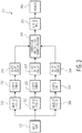
- FIG. 2 illustrates an embodiment of a secure circuit using redundant secure circuits with additional delays.
- the secure circuit includes crypto cores 210 and 215, comparison and infection counter measure circuit 220, and delay circuits 230, 235, and 240.
- Crypto core 210 receives the input data 205.
- the crypto core 210 then processes the input data and produces an output that is fed into a delay circuit 230.
- the delay circuit 230 delays the output of the crypto core 210 by a time N.
- the output of the delay circuit is then input to the comparison and infection counter measure circuit 220.
- the input data 205 is also input to a delay circuit 235 that delays the input 205 by a time N.
- the crypto core 215 then receives the delayed input from the delay circuit 235.
- the output of the crypto core 215 is then input into a comparison and infection counter measure circuit 220. If the outputs of the crypto core 215 and the delay circuit 230 match, then crypto core outputs are considered valid. If the outputs of crypto core 215 and the delay circuit 230 do not match, then an error value is produced by the comparison and infection counter measure circuit 220 as the result 225 where errors are inserted in the result 225 to affect a larger number of bits than the number of bits corrupted by the attacker.
- the output of the comparison and infection counter measure circuit 220 may optionally be input to a delay element 240 that delays the assertion of the result 225 by a time M.
- the delay circuit 240 may be optionally added where the delay circuit 240 delays the output by a time M.
- the difficulty for the attacker may be further increased by varying the delay N over time, e.g., based on the output of a random number generator.
- the value of N may be changed at some regular or even varying period.
- FIG. 3 illustrates another embodiment of a secure circuit using redundant secure circuits with additional delays.
- the secure circuit 300 illustrates how the use of the delays may be generalized to more than two instances of secure circuit.
- the secure circuit includes crypto cores 312, 322, and 332, comparison and infection counter measure circuit 340, and delay circuits 310, 314, 320, 324, 330, 334, and 345.
- the delay circuits 310, 320, and 330 receive the input data 305.
- the delay circuits 310, 320, and 330 each output the input data delayed by aN, bN, and cN respectively.
- N is a time delay.
- the values a, b, and c are scalar values from 0 to n that are chosen to be different for each delay circuit so that the total delay is different for each circuit.
- the outputs of the delay circuits 310, 320, and 330 are input to the crypto cores 312, 322, and 332 respectively.
- the outputs of the crypto cores 312, 322, and 332 are then input to delay circuits 314, 324, and 334 respectively.
- Delay circuits 314, 324, and 334 have delays of (n-a)N, (n-b)N, and (n-c)N respectively.
- the outputs of delay circuits 314, 324, and 334 are then input to the comparison and infection counter measure circuit 340.
- the comparison and infection counter measure circuit 340 may optionally be input to a delay element 345 that delays the result 350 by a time M.
- the values for N may also be chosen randomly, and the value of M could then be selected such that M+nN is constant as before. This will hide the randomness of the values.
- the values of scalars a, b, and c may be fixed or randomly selected. At least two of the scalar values a, b, and c need to different so that the input data is processed at different times in at least two of the crypto cores.
- the secure circuit 300 may be extended to an even larger number of instances by adding additional crypto cores and associated delays. Further, the secure circuit 300 may be simplified by setting a to 0 and b to n. As a result, the delay 310 and the delay 324 may be deleted from the circuit as each of these delays would be zero.
- FIGs. 1-3 may also be implemented completely in hardware or a combination of both hardware and software. Any combination of specific software running on a processor to implement the embodiments of the invention, constitute a specific dedicated machine.
- Various embodiments relate to a circuit, including: a first secure circuit configured to receive an input and to produce a first output; a first delay circuit configured to receive the first output and to produce a first delayed output delayed by a time N; a second delay circuit configured to receive the input and to produce a delayed input delayed by a time N; a second secure circuit configured to receive the delayed input and to produce a second delayed output; and a comparator configured to compare the first delayed output to the second delayed output and to produce a result, wherein the result is one of the first delayed output or second delayed output when the first delayed output matches the second delayed output and the result is an error value when the first delayed output does not match the second delayed output.
- non-transitory machine-readable storage medium will be understood to exclude a transitory propagation signal but to include all forms of volatile and nonvolatile memory.
Landscapes
- Engineering & Computer Science (AREA)
- Physics & Mathematics (AREA)
- Computer Security & Cryptography (AREA)
- Nonlinear Science (AREA)
- Computer Hardware Design (AREA)
- Mathematical Physics (AREA)
- General Engineering & Computer Science (AREA)
- Computing Systems (AREA)
- Theoretical Computer Science (AREA)
- Computer Networks & Wireless Communication (AREA)
- Signal Processing (AREA)
- General Physics & Mathematics (AREA)
- Software Systems (AREA)
- Hardware Redundancy (AREA)
- Storage Device Security (AREA)
- Manipulation Of Pulses (AREA)
Abstract
Description
- Various exemplary embodiments disclosed herein relate generally to fault attack protection against synchronized fault injections.
- Various schemes have been developed for attacking cryptographic hardware including fault attacks where faults are injected into the cryptographic hardware. An attacker can then induce faults and analyze the results to obtain secret information regarding the cryptographic hardware such as a cryptographic key.
- A summary of various exemplary embodiments is presented below. Some simplifications and omissions may be made in the following summary, which is intended to highlight and introduce some aspects of the various exemplary embodiments, but not to limit the scope of the invention. Detailed descriptions of an exemplary embodiment adequate to allow those of ordinary skill in the art to make and use the inventive concepts will follow in later sections.
- Various embodiments relate to a circuit, including: a first secure circuit configured to receive an input and to produce a first output; a first delay circuit configured to receive the first output and to produce a first delayed output delayed by a time N; a second delay circuit configured to receive the input and to produce a delayed input delayed by a time N; a second secure circuit configured to receive the delayed input and to produce a second delayed output; and a comparator configured to compare the first delayed output to the second delayed output and to produce a result, wherein the result is one of the first delayed output or second delayed output when the first delayed output matches the second delayed output and the result is an error value when the first delayed output does not match the second delayed output.
- Various embodiments are described, wherein the value of N is randomly selected.
- Various embodiments are described, wherein the value of N is periodically changed.
- Various embodiments are described, further including: a third delay circuit configured to receive the result and to produce a delayed result delayed by a time M.
- Various embodiments are described, wherein the value of N is randomly selected and the value of M = x - N where x is a constant total delay value.
- Various embodiments are described, wherein the value of N and M are periodically changed.
- A method of securely producing an output by a circuit, including: receiving an input by a first secure circuit and producing a first output; receiving the output by a first delay circuit and producing a first delayed output delayed by a time N; receiving the input by a second delay circuit and producing a delayed input delayed by a time N; receiving the delayed input by a second secure circuit and producing a second delayed output; and comparing by a comparator the first delayed output to the second delayed output and producing a result, wherein the result is one of the first delayed output or second delayed output when the first delayed output matches the second delayed output and the result is an error value when the first delayed output does not match the second delayed output.
- Various embodiments are described, wherein the value of N is randomly selected.
- Various embodiments are described, wherein the value of N is periodically changed.
- Various embodiments are described wherein further including: receiving the result by a third delay circuit and producing a delayed result delayed by a time M.
- The method of claim 10, wherein the value of N is randomly selected and the value of M = x - N where x is a constant total delay value.
- Various embodiments are described, wherein the value of N and M are periodically changed.
- Further various embodiments relate to a circuit, including: a first delay circuit configured to receive an input and to produce a first delayed input delayed by a time a•N, where N is a time delay and a is a scalar value from 0 to n; a second delay circuit configured to receive the input and to produce a second delayed input delayed by a time b•N, where b is a scalar value from 0 to n; a third delay circuit configured to receive the input and to produce a third delayed input delayed by a time c•N, where c is a scalar value from 0 to n; a first secure circuit configured to receive the first delayed input and to produce a first delayed output; a second secure circuit configured to receive the second delayed input and to produce a second delayed output; a third secure circuit configured to receive the third delayed input and to produce a third delayed output; a fourth delay circuit configured to receive the first delayed output and to produce a fourth delayed output delayed by a time (n-a)•N; a fifth delay circuit configured to receive the second delayed output and to produce a fifth delayed output delayed by a time (n-b)•N; a sixth delay circuit configured to receive the third delayed output and to produce a sixth delayed output delayed by a time (n-c)•N; and a comparator configured to compare the fourth delayed output, the fifth delayed output, and sixth delayed output and to produce a result, wherein the result is one of the fourth delayed output, fifth delayed output, or second delayed output when the fourth delayed output, the fifth delayed output, and sixth delayed output are all equal to one another and the result is an error value otherwise.
- Various embodiments are described, wherein the value of N is randomly selected.
- Various embodiments are described, wherein the value of N is periodically changed.
- Various embodiments are described, further including: a third delay circuit configured to receive the result and to produce a delayed result delayed by a time M.
- Various embodiments are described, wherein the value of N is randomly selected and the value of M = x - N where x is a constant total delay value.
- Various embodiments are described, wherein the value of N and M are periodically changed.
- Various embodiments are described, wherein at least two of the scalar values a, b, and c are different.
- In order to better understand various exemplary embodiments, reference is made to the accompanying drawings, wherein:
-
FIG. 1 illustrates a secure circuit using redundant secure circuits; -
FIG. 2 illustrates an embodiment of a secure circuit using redundant secure circuits with additional delays; and -
FIG. 3 illustrates another embodiment of a secure circuit using redundant secure circuits with additional delays. - To facilitate understanding, identical reference numerals have been used to designate elements having substantially the same or similar structure and/or substantially the same or similar function.
- The description and drawings illustrate the principles of the invention. It will thus be appreciated that those skilled in the art will be able to devise various arrangements that, although not explicitly described or shown herein, embody the principles of the invention and are included within its scope. Furthermore, all examples recited herein are principally intended expressly to be for pedagogical purposes to aid the reader in understanding the principles of the invention and the concepts contributed by the inventor(s) to furthering the art and are to be construed as being without limitation to such specifically recited examples and conditions. Additionally, the term, "or," as used herein, refers to a non-exclusive or (i.e., and/or), unless otherwise indicated (e.g., "or else" or "or in the alternative"). Also, the various embodiments described herein are not necessarily mutually exclusive, as some embodiments can be combined with one or more other embodiments to form new embodiments.
- Attackers of secure circuits (such as cryptographic accelerators) may attempt to corrupt the outputs of these circuits with fine granularity (ideally bit by bit) in order to observe the reaction of the overall device or to create a favorable reaction. Fault attacks such as laser attacks may be employed for this purpose. In such an attack, a laser beam is focused on a specific part of a circuit to cause a fault in a specific bit or set of bits. By observing inputs and outputs to the secure circuit during normal operation and then the operation of the circuit when faults are induced, an attacker may perform statistical and/or other analysis to gain information regarding secure information such as a cryptographic key.
- As a counter measure against such fault attacks, secure circuits may be implemented redundantly, for example with two or more instantiations of the secure circuit, and the outputs of the redundant secure circuits combined with comparison logic. That is the output of the two different circuits are compared, and if they match then the outputs are valid, and if the outputs do not match then the outputs are invalid.
FIG. 1 illustrates asecure circuit 100 using redundant secure circuits. Specifically,crypto cores same input data 105. The operation of the twocrypto cores crypto cores counter measure circuit 120. If the outputs of the two crypto cores match, then the outputs of thecrypto cores result 125. If the outputs of two crypto cores do not match, then an error value is produced by the comparison and infectioncounter measure circuit 120 as the result where errors are inserted in the result to affect a larger number of bits than the number of bits corrupted by the attacker. As a result, an attacker trying to modify only a few bits of theresult 125 would instead end up disturbing a large number of bits. This limits what an attacker can learn with such attacks. The comparison and infection counter measure circuit may also be called a comparator. - Previously it was thought to be difficult to coordinate attacks on multiple instances of a security circuit at precisely the correct time. This redundant implementation of security circuits requires an attacker to attack all instances simultaneously and with precise timing which is much harder to accomplish. However, researchers have devised new methods to coordinate the attack on all redundant instances of the security circuit at the same time, e.g. using optical methods such as splitting a laser beam with a prism. These methods overcome the previously high barrier to synchronize the attacks.
- Embodiments that protect the circuit against these simple synchronization attacks will now be described. Such attacks may be countered by inserting delays in the circuits at different locations in the redundant instances.
-
FIG. 2 illustrates an embodiment of a secure circuit using redundant secure circuits with additional delays. Specifically, the secure circuit includescrypto cores counter measure circuit 220, and delaycircuits Crypto core 210 receives theinput data 205. Thecrypto core 210 then processes the input data and produces an output that is fed into adelay circuit 230. Thedelay circuit 230 delays the output of thecrypto core 210 by a time N. The output of the delay circuit is then input to the comparison and infectioncounter measure circuit 220. Theinput data 205 is also input to adelay circuit 235 that delays theinput 205 by a time N. Thecrypto core 215 then receives the delayed input from thedelay circuit 235. The output of thecrypto core 215 is then input into a comparison and infectioncounter measure circuit 220. If the outputs of thecrypto core 215 and thedelay circuit 230 match, then crypto core outputs are considered valid. If the outputs ofcrypto core 215 and thedelay circuit 230 do not match, then an error value is produced by the comparison and infectioncounter measure circuit 220 as theresult 225 where errors are inserted in theresult 225 to affect a larger number of bits than the number of bits corrupted by the attacker. The output of the comparison and infectioncounter measure circuit 220 may optionally be input to adelay element 240 that delays the assertion of theresult 225 by a time M. - In
FIG. 2 , it can be seen that the inputs forredundant crypto core 215 will be available only at a certain delay N after the input has become available forcrypto core 210. As a result,crypto core 210 will produce its output earlier thencrypto core 215. However, as the output ofcrypto core 210 is delayed by the same amount of time N, the comparison of the output of thecrypto cores - As noted, the
delay circuit 240 may be optionally added where thedelay circuit 240 delays the output by a time M. The difficulty for the attacker may be further increased by varying the delay N over time, e.g., based on the output of a random number generator. The value of N may be changed at some regular or even varying period. Further, the randomness of the delay N may be hidden by keeping the sum of M + N constant. In this situation, M is selected as M = x - N, where x is a fix total delay and N randomly chosen. -
FIG. 3 illustrates another embodiment of a secure circuit using redundant secure circuits with additional delays. Thesecure circuit 300 illustrates how the use of the delays may be generalized to more than two instances of secure circuit. Specifically, the secure circuit includescrypto cores counter measure circuit 340, and delaycircuits delay circuits input data 305. Thedelay circuits delay circuits crypto cores crypto cores circuits circuits delay circuits counter measure circuit 340. If the outputs of all thedelay circuits delay circuits counter measure circuit 340 as theresult 350 where errors are inserted in theresult 350 to affect a larger number of bits than the number of bits corrupted by the attacker. The output of the comparison and infectioncounter measure circuit 340 may optionally be input to adelay element 345 that delays theresult 350 by a time M. In this embodiment the values for N may also be chosen randomly, and the value of M could then be selected such that M+nN is constant as before. This will hide the randomness of the values. Further, the values of scalars a, b, and c may be fixed or randomly selected. At least two of the scalar values a, b, and c need to different so that the input data is processed at different times in at least two of the crypto cores. Thesecure circuit 300 may be extended to an even larger number of instances by adding additional crypto cores and associated delays. Further, thesecure circuit 300 may be simplified by setting a to 0 and b to n. As a result, thedelay 310 and thedelay 324 may be deleted from the circuit as each of these delays would be zero. - The embodiments described in
FIGs. 1-3 may also be implemented completely in hardware or a combination of both hardware and software. Any combination of specific software running on a processor to implement the embodiments of the invention, constitute a specific dedicated machine. - Various embodiments relate to a circuit, including: a first secure circuit configured to receive an input and to produce a first output; a first delay circuit configured to receive the first output and to produce a first delayed output delayed by a time N; a second delay circuit configured to receive the input and to produce a delayed input delayed by a time N; a second secure circuit configured to receive the delayed input and to produce a second delayed output; and a comparator configured to compare the first delayed output to the second delayed output and to produce a result, wherein the result is one of the first delayed output or second delayed output when the first delayed output matches the second delayed output and the result is an error value when the first delayed output does not match the second delayed output.
- As used herein, the term "non-transitory machine-readable storage medium" will be understood to exclude a transitory propagation signal but to include all forms of volatile and nonvolatile memory.
- It should be appreciated by those skilled in the art that any block diagrams herein represent conceptual views of illustrative circuitry embodying the principles of the invention.
- Although the various exemplary embodiments have been described in detail with particular reference to certain exemplary aspects thereof, it should be understood that the invention is capable of other embodiments and its details are capable of modifications in various obvious respects. As is readily apparent to those skilled in the art, variations and modifications can be affected while remaining within the spirit and scope of the invention. Accordingly, the foregoing disclosure, description, and figures are for illustrative purposes only and do not in any way limit the invention, which is defined only by the claims.
Claims (12)
- A circuit, comprising:a first secure circuit configured to receive an input and to produce a first output;a first delay circuit configured to receive the first output and to produce a first delayed output delayed by a time N;a second delay circuit configured to receive the input and to produce a delayed input delayed by a time N;a second secure circuit configured to receive the delayed input and to produce a second delayed output; anda comparator configured to compare the first delayed output to the second delayed output and to produce a result, wherein the result is one of the first delayed output or second delayed output when the first delayed output matches the second delayed output and the result is an error value when the first delayed output does not match the second delayed output.
- The circuit of claim 1, wherein the value of N is randomly selected.
- The circuit of claim 1 or 2, wherein the value of N is periodically changed.
- The circuit of any preceding claim, further comprising:
a third delay circuit configured to receive the result and to produce a delayed result delayed by a time M. - The circuit of claim 4, wherein the value of N is randomly selected and the value of M = x - N where x is a constant total delay value.
- The circuit of claim 4 or 5, wherein the value of N and M are periodically changed.
- A method of securely producing an output by a circuit, comprising:receiving an input by a first secure circuit and producing a first output;receiving the output by a first delay circuit and producing a first delayed output delayed by a time N;receiving the input by a second delay circuit and producing a delayed input delayed by a time N;receiving the delayed input by a second secure circuit and producing a second delayed output; andcomparing by a comparator the first delayed output to the second delayed output and producing a result, wherein the result is one of the first delayed output or second delayed output when the first delayed output matches the second delayed output and the result is an error value when the first delayed output does not match the second delayed output.
- The method of claim 7, wherein the value of N is randomly selected.
- The method of claim 7 or 8, wherein the value of N is periodically changed.
- The method of any of claims 7 to 9, further comprising:
receiving the result by a third delay circuit and producing a delayed result delayed by a time M. - The method of any of claims 7 to 10, wherein the value of N is randomly selected and the value of M = x - N where x is a constant total delay value.
- The method of claim 11, wherein the value of N and M are periodically changed.
Applications Claiming Priority (1)
| Application Number | Priority Date | Filing Date | Title |
|---|---|---|---|
| US16/006,457 US10305479B1 (en) | 2018-06-12 | 2018-06-12 | Fault attack protection against synchronized fault injections |
Publications (2)
| Publication Number | Publication Date |
|---|---|
| EP3582434A1 true EP3582434A1 (en) | 2019-12-18 |
| EP3582434B1 EP3582434B1 (en) | 2022-01-12 |
Family
ID=66636440
Family Applications (1)
| Application Number | Title | Priority Date | Filing Date |
|---|---|---|---|
| EP19179233.2A Active EP3582434B1 (en) | 2018-06-12 | 2019-06-10 | Fault attack protection against synchronized fault injections |
Country Status (3)
| Country | Link |
|---|---|
| US (1) | US10305479B1 (en) |
| EP (1) | EP3582434B1 (en) |
| CN (1) | CN110598484B (en) |
Cited By (1)
| Publication number | Priority date | Publication date | Assignee | Title |
|---|---|---|---|---|
| EP4738765A1 (en) * | 2024-10-31 | 2026-05-06 | Nxp B.V. | A lightweight fault countermeasure for post-quantum kems |
Families Citing this family (5)
| Publication number | Priority date | Publication date | Assignee | Title |
|---|---|---|---|---|
| CN110188053B (en) * | 2019-05-30 | 2020-12-01 | 北京润科通用技术有限公司 | Airborne data bus delay fault injection equipment and method |
| US11244046B2 (en) | 2019-09-16 | 2022-02-08 | Nuvoton Technology Corporation | Data-sampling integrity check using gated clock |
| US11321457B2 (en) * | 2019-09-16 | 2022-05-03 | Nuvoton Technology Corporation | Data-sampling integrity check by sampling using flip-flops with relative delay |
| FR3123469B1 (en) * | 2021-05-26 | 2023-09-01 | Idemia France | IMPROVED INFECTION COUNTERMEASURES |
| KR20230029113A (en) | 2021-08-23 | 2023-03-03 | 삼성전자주식회사 | Electronic device |
Citations (1)
| Publication number | Priority date | Publication date | Assignee | Title |
|---|---|---|---|---|
| US20110029828A1 (en) * | 2009-07-30 | 2011-02-03 | Stmicroelectronics (Rousset) Sas | Fault injection detector in an integrated circuit |
Family Cites Families (50)
| Publication number | Priority date | Publication date | Assignee | Title |
|---|---|---|---|---|
| US5032708A (en) * | 1989-08-10 | 1991-07-16 | International Business Machines Corp. | Write-once-read-once batteryless authentication token |
| US5604806A (en) * | 1995-01-20 | 1997-02-18 | Ericsson Inc. | Apparatus and method for secure radio communication |
| GB2397452B (en) * | 2003-01-16 | 2005-07-13 | Toshiba Res Europ Ltd | A quantum communication system |
| GB2399220B (en) * | 2003-03-06 | 2005-07-13 | Toshiba Res Europ Ltd | Photonic quantum information system using unpolarised light |
| GB2419264B (en) * | 2003-08-18 | 2006-12-27 | Toshiba Res Europ Ltd | A quantum communication system and a receiver for a quantum communication system |
| JP4304298B2 (en) * | 2004-02-13 | 2009-07-29 | 日本電気株式会社 | Communication system and synchronization method thereof |
| US7089099B2 (en) * | 2004-07-30 | 2006-08-08 | Automotive Technologies International, Inc. | Sensor assemblies |
| US7590880B1 (en) * | 2004-09-13 | 2009-09-15 | National Semiconductor Corporation | Circuitry and method for detecting and protecting against over-clocking attacks |
| WO2008108984A2 (en) * | 2007-03-01 | 2008-09-12 | Soapstone Networks, Inc. | Software control plane for switches and routers |
| GB2457253B (en) * | 2008-02-07 | 2010-08-11 | Ericsson Telefon Ab L M | Controlling media distribution |
| US8683210B2 (en) * | 2008-11-21 | 2014-03-25 | Verayo, Inc. | Non-networked RFID-PUF authentication |
| WO2011064613A1 (en) * | 2009-11-25 | 2011-06-03 | Serela | Card sharing countermeasures |
| US8756684B2 (en) * | 2010-03-01 | 2014-06-17 | Emc Corporation | System and method for network security including detection of attacks through partner websites |
| SG183332A1 (en) * | 2010-03-01 | 2012-09-27 | Silver Tail Systems | System and method for network security including detection of attacks through partner websites |
| US8861535B2 (en) * | 2010-05-21 | 2014-10-14 | Cisco Technology, Inc. | Multi-tiered paging support using paging priority |
| EP3495974B1 (en) * | 2011-03-30 | 2022-02-16 | Irdeto B.V. | Enabling a software application to be executed on a mobile station |
| US20130044798A1 (en) * | 2011-08-18 | 2013-02-21 | Microsoft Corporation | Side Channel Communications |
| EP2789138B1 (en) * | 2011-12-06 | 2016-09-14 | Seven Networks, LLC | A mobile device and method to utilize the failover mechanisms for fault tolerance provided for mobile traffic management and network/device resource conservation |
| US9423819B2 (en) * | 2012-07-16 | 2016-08-23 | The Board of Trustees of the Leland Stanford Univeristy | Optical quantum random number generator |
| US9055100B2 (en) * | 2013-04-06 | 2015-06-09 | Citrix Systems, Inc. | Systems and methods for HTTP-Body DoS attack prevention with adaptive timeout |
| AU2014331655A1 (en) * | 2013-10-11 | 2016-05-26 | Marcio Marc Abreu | Method and apparatus for biological evaluation |
| WO2015061715A1 (en) * | 2013-10-24 | 2015-04-30 | Internet Infrastructure Services Corporation | Methods of dynamically securing electronic devices and other communications through environmental and system measurements leveraging tailored trustworthy spaces |
| US9405892B2 (en) * | 2013-11-26 | 2016-08-02 | At&T Intellectual Property I, L.P. | Preventing spoofing attacks for bone conduction applications |
| CA2938318C (en) * | 2014-01-30 | 2023-10-03 | Nasdaq, Inc. | Systems and methods for continuous active data security |
| EP3152859A1 (en) | 2014-06-04 | 2017-04-12 | Giesecke & Devrient GmbH | Method for enhanced security of computational device with multiple cores |
| US9559066B2 (en) * | 2014-06-12 | 2017-01-31 | Broadcom Corporation | Systems and methods for detecting and preventing optical attacks |
| US9523736B2 (en) * | 2014-06-19 | 2016-12-20 | Nuvoton Technology Corporation | Detection of fault injection attacks using high-fanout networks |
| CN104101486B (en) | 2014-07-16 | 2016-07-13 | 中国科学院上海光学精密机械研究所 | Dual Beam Delayed Laser Damage Test System |
| FR3026253B1 (en) * | 2014-09-19 | 2016-12-09 | Commissariat Energie Atomique | SYSTEM AND METHOD FOR SECURING AN ELECTRONIC CIRCUIT |
| US10013581B2 (en) * | 2014-10-07 | 2018-07-03 | Nuvoton Technology Corporation | Detection of fault injection attacks |
| EP3234857B1 (en) * | 2014-12-15 | 2019-08-21 | Stc.Unm | Reliability enhancement methods for physically unclonable function bitstring generation |
| US20160217399A1 (en) * | 2015-01-22 | 2016-07-28 | Elementum Scm (Cayman) Ltd. | Method and system for monitoring shipments in a supply and/or logistics chain |
| US10291957B2 (en) * | 2015-05-22 | 2019-05-14 | Telefonaktiebolaget Lm Ericsson (Publ) | Quicker IPTV channel with static group on IGMP loopback interface |
| US10356068B2 (en) * | 2015-07-14 | 2019-07-16 | Avocado Systems Inc. | Security key generator module for security sensitive applications |
| US9946231B2 (en) * | 2015-09-01 | 2018-04-17 | The Florida International University Board Of Trustees | Detection of and responses to time delays in networked control systems |
| JP6899378B2 (en) * | 2015-09-03 | 2021-07-07 | シグニファイ ホールディング ビー ヴィSignify Holding B.V. | Network node |
| US9961093B1 (en) * | 2015-09-30 | 2018-05-01 | EMC IP Holding Company LLC | Monitoring for reverse-connection network activity to detect a remote-administration tool |
| GB2547025A (en) * | 2016-02-05 | 2017-08-09 | Thales Holdings Uk Plc | A method of data transfer, a method of controlling use of data and a cryptographic device |
| US10958414B2 (en) * | 2016-02-23 | 2021-03-23 | Google Llc | Clock period randomization for defense against cryptographic attacks |
| US20170364683A1 (en) * | 2016-06-17 | 2017-12-21 | Google Inc. | Computing device secure boot |
| US10678924B2 (en) * | 2016-08-10 | 2020-06-09 | Qualcomm Incorporated | Hardware-based software-resilient user privacy exploiting ephemeral data retention of volatile memory |
| US10255314B2 (en) * | 2017-03-16 | 2019-04-09 | International Business Machines Corporation | Comparison of block based volumes with ongoing inputs and outputs |
| WO2018183008A1 (en) * | 2017-03-31 | 2018-10-04 | Airprox USA, Inc. | Virtual radar apparatus and method |
| US10015756B1 (en) * | 2017-04-11 | 2018-07-03 | Deborah T Bullington | System and method for adjusting signal strength for medical appointment progress tracking |
| US10057373B1 (en) * | 2017-05-15 | 2018-08-21 | Palantir Technologies Inc. | Adaptive computation and faster computer operation |
| GB2564446B (en) * | 2017-07-10 | 2020-01-22 | Toshiba Kk | A Quantum communication component, receiver and system |
| US10438190B2 (en) * | 2017-07-18 | 2019-10-08 | Square, Inc. | Devices with on-board physically unclonable functions |
| US10263793B2 (en) * | 2017-07-18 | 2019-04-16 | Square, Inc. | Devices with modifiable physically unclonable functions |
| US10819528B2 (en) * | 2017-07-18 | 2020-10-27 | Square, Inc. | Device security with physically unclonable functions |
| US10705842B2 (en) * | 2018-04-02 | 2020-07-07 | Intel Corporation | Hardware accelerators and methods for high-performance authenticated encryption |
-
2018
- 2018-06-12 US US16/006,457 patent/US10305479B1/en active Active
-
2019
- 2019-06-10 EP EP19179233.2A patent/EP3582434B1/en active Active
- 2019-06-12 CN CN201910508552.6A patent/CN110598484B/en active Active
Patent Citations (1)
| Publication number | Priority date | Publication date | Assignee | Title |
|---|---|---|---|---|
| US20110029828A1 (en) * | 2009-07-30 | 2011-02-03 | Stmicroelectronics (Rousset) Sas | Fault injection detector in an integrated circuit |
Non-Patent Citations (3)
| Title |
|---|
| BAR-EL H ET AL: "The Sorcerer's Apprentice Guide to Fault Attacks", PROCEEDINGS OF THE IEEE, IEEE. NEW YORK, US, vol. 94, no. 2, 1 February 2006 (2006-02-01), pages 370 - 382, XP011442695, ISSN: 0018-9219, DOI: 10.1109/JPROC.2005.862424 * |
| FERNANDA LIMA ET AL: "Designing fault tolerant systems into SRAM-based FPGAs", PROCEEDINGS OF THE 40TH. ANNUAL DESIGN AUTOMATION CONFERENCE. (DAC). ANAHEIM, CA, JUNE 2 - 6, 2003; [PROCEEDINGS OF THE DESIGN AUTOMATION CONFERENCE], NEW YORK, NY : ACM, US, 2 June 2003 (2003-06-02), pages 650 - 655, XP058294041, ISBN: 978-1-58113-688-3, DOI: 10.1145/775832.775997 * |
| KANEKAWA N ET AL: "Fault detection and recovery coverage improvement by clock synchronized duplicated systems with optimal time diversity", FAULT-TOLERANT COMPUTING, 1998. DIGEST OF PAPERS. TWENTY-EIGHTH ANNUAL INTERNATIONAL SYMPOSIUM ON MUNICH, GERMANY 23-25 JUNE 1998, LOS ALAMITOS, CA, USA,IEEE COMPUT. SOC, US, 23 June 1998 (1998-06-23), pages 196 - 200, XP032384995, ISBN: 978-0-8186-8470-8, DOI: 10.1109/FTCS.1998.689470 * |
Cited By (1)
| Publication number | Priority date | Publication date | Assignee | Title |
|---|---|---|---|---|
| EP4738765A1 (en) * | 2024-10-31 | 2026-05-06 | Nxp B.V. | A lightweight fault countermeasure for post-quantum kems |
Also Published As
| Publication number | Publication date |
|---|---|
| US10305479B1 (en) | 2019-05-28 |
| CN110598484B (en) | 2024-06-11 |
| CN110598484A (en) | 2019-12-20 |
| EP3582434B1 (en) | 2022-01-12 |
Similar Documents
| Publication | Publication Date | Title |
|---|---|---|
| US10305479B1 (en) | Fault attack protection against synchronized fault injections | |
| US10833871B2 (en) | System and method for deterministic signing of a message using a multi-party computation (MPC) process | |
| US11151290B2 (en) | Tamper-resistant component networks | |
| CN112689837B (en) | Cryptographic integrated circuit and method for detecting fault injection attacks on cryptographic devices | |
| EP3503466B1 (en) | Countermeasures to frequency alteration attacks on ring oscillator based physical unclonable functions | |
| US20090252327A1 (en) | Combination white box/black box cryptographic processes and apparatus | |
| US20200034549A1 (en) | Method and apparatus for secure external access of the puf information to an authorized entity | |
| US7162031B1 (en) | Method and device for cryptographically processing data | |
| US12019738B2 (en) | Fault injection attack system | |
| US9083515B1 (en) | Forward secure pseudorandom number generation resilient to forward clock attacks | |
| EP3057029B1 (en) | Improved encryption and authentication method and apparatus | |
| US10630471B1 (en) | System and method for enforcement of correctness for key derivation | |
| Soleimany et al. | Practical multiple persistent faults analysis | |
| EP3214567B1 (en) | Secure external update of memory content for a certain system on chip | |
| CN110943841A (en) | Password authentication using white-box encryption | |
| Fahr | The Effects of Side-Channel Attacks on Post-Quantum Cryptography: Influencing FrodoKEM Key Generation Using the Rowhammer Exploit | |
| CN108737073B (en) | Method and device for resisting energy analysis attack in block encryption operation | |
| KR102800489B1 (en) | Integrated circuit for challenge-response physically unclonable function and method for using the same | |
| Luo et al. | Differential fault analysis of SHA-3 under relaxed fault models | |
| CN115001656A (en) | Selected plaintext persistence fault analysis method and device for block cipher | |
| Guo et al. | Persistent fault analysis against SM4 implementations in libraries Crypto++ and GMSSL | |
| KR102515902B1 (en) | Authentication device using physical unclonable function | |
| Jendral et al. | Correction Fault Attack on CROSS under Unknown Bit Flips | |
| US11212111B2 (en) | Method for synchronized signature with additive RSA key splitting using a sliding window | |
| US9411952B2 (en) | Method for authentication |
Legal Events
| Date | Code | Title | Description |
|---|---|---|---|
| PUAI | Public reference made under article 153(3) epc to a published international application that has entered the european phase |
Free format text: ORIGINAL CODE: 0009012 |
|
| STAA | Information on the status of an ep patent application or granted ep patent |
Free format text: STATUS: THE APPLICATION HAS BEEN PUBLISHED |
|
| AK | Designated contracting states |
Kind code of ref document: A1 Designated state(s): AL AT BE BG CH CY CZ DE DK EE ES FI FR GB GR HR HU IE IS IT LI LT LU LV MC MK MT NL NO PL PT RO RS SE SI SK SM TR |
|
| AX | Request for extension of the european patent |
Extension state: BA ME |
|
| STAA | Information on the status of an ep patent application or granted ep patent |
Free format text: STATUS: REQUEST FOR EXAMINATION WAS MADE |
|
| 17P | Request for examination filed |
Effective date: 20200618 |
|
| RBV | Designated contracting states (corrected) |
Designated state(s): AL AT BE BG CH CY CZ DE DK EE ES FI FR GB GR HR HU IE IS IT LI LT LU LV MC MK MT NL NO PL PT RO RS SE SI SK SM TR |
|
| STAA | Information on the status of an ep patent application or granted ep patent |
Free format text: STATUS: EXAMINATION IS IN PROGRESS |
|
| 17Q | First examination report despatched |
Effective date: 20200810 |
|
| GRAP | Despatch of communication of intention to grant a patent |
Free format text: ORIGINAL CODE: EPIDOSNIGR1 |
|
| STAA | Information on the status of an ep patent application or granted ep patent |
Free format text: STATUS: GRANT OF PATENT IS INTENDED |
|
| RIC1 | Information provided on ipc code assigned before grant |
Ipc: H04L 9/00 20060101AFI20210717BHEP Ipc: H03K 5/13 20140101ALI20210717BHEP Ipc: H03K 5/24 20060101ALI20210717BHEP |
|
| INTG | Intention to grant announced |
Effective date: 20210818 |
|
| GRAS | Grant fee paid |
Free format text: ORIGINAL CODE: EPIDOSNIGR3 |
|
| GRAA | (expected) grant |
Free format text: ORIGINAL CODE: 0009210 |
|
| STAA | Information on the status of an ep patent application or granted ep patent |
Free format text: STATUS: THE PATENT HAS BEEN GRANTED |
|
| AK | Designated contracting states |
Kind code of ref document: B1 Designated state(s): AL AT BE BG CH CY CZ DE DK EE ES FI FR GB GR HR HU IE IS IT LI LT LU LV MC MK MT NL NO PL PT RO RS SE SI SK SM TR |
|
| REG | Reference to a national code |
Ref country code: GB Ref legal event code: FG4D |
|
| REG | Reference to a national code |
Ref country code: CH Ref legal event code: EP |
|
| REG | Reference to a national code |
Ref country code: DE Ref legal event code: R096 Ref document number: 602019010792 Country of ref document: DE |
|
| REG | Reference to a national code |
Ref country code: IE Ref legal event code: FG4D |
|
| REG | Reference to a national code |
Ref country code: AT Ref legal event code: REF Ref document number: 1463102 Country of ref document: AT Kind code of ref document: T Effective date: 20220215 |
|
| REG | Reference to a national code |
Ref country code: LT Ref legal event code: MG9D |
|
| REG | Reference to a national code |
Ref country code: NL Ref legal event code: MP Effective date: 20220112 |
|
| REG | Reference to a national code |
Ref country code: AT Ref legal event code: MK05 Ref document number: 1463102 Country of ref document: AT Kind code of ref document: T Effective date: 20220112 |
|
| PG25 | Lapsed in a contracting state [announced via postgrant information from national office to epo] |
Ref country code: NL Free format text: LAPSE BECAUSE OF FAILURE TO SUBMIT A TRANSLATION OF THE DESCRIPTION OR TO PAY THE FEE WITHIN THE PRESCRIBED TIME-LIMIT Effective date: 20220112 |
|
| PG25 | Lapsed in a contracting state [announced via postgrant information from national office to epo] |
Ref country code: SE Free format text: LAPSE BECAUSE OF FAILURE TO SUBMIT A TRANSLATION OF THE DESCRIPTION OR TO PAY THE FEE WITHIN THE PRESCRIBED TIME-LIMIT Effective date: 20220112 Ref country code: RS Free format text: LAPSE BECAUSE OF FAILURE TO SUBMIT A TRANSLATION OF THE DESCRIPTION OR TO PAY THE FEE WITHIN THE PRESCRIBED TIME-LIMIT Effective date: 20220112 Ref country code: PT Free format text: LAPSE BECAUSE OF FAILURE TO SUBMIT A TRANSLATION OF THE DESCRIPTION OR TO PAY THE FEE WITHIN THE PRESCRIBED TIME-LIMIT Effective date: 20220512 Ref country code: NO Free format text: LAPSE BECAUSE OF FAILURE TO SUBMIT A TRANSLATION OF THE DESCRIPTION OR TO PAY THE FEE WITHIN THE PRESCRIBED TIME-LIMIT Effective date: 20220412 Ref country code: LT Free format text: LAPSE BECAUSE OF FAILURE TO SUBMIT A TRANSLATION OF THE DESCRIPTION OR TO PAY THE FEE WITHIN THE PRESCRIBED TIME-LIMIT Effective date: 20220112 Ref country code: HR Free format text: LAPSE BECAUSE OF FAILURE TO SUBMIT A TRANSLATION OF THE DESCRIPTION OR TO PAY THE FEE WITHIN THE PRESCRIBED TIME-LIMIT Effective date: 20220112 Ref country code: ES Free format text: LAPSE BECAUSE OF FAILURE TO SUBMIT A TRANSLATION OF THE DESCRIPTION OR TO PAY THE FEE WITHIN THE PRESCRIBED TIME-LIMIT Effective date: 20220112 Ref country code: BG Free format text: LAPSE BECAUSE OF FAILURE TO SUBMIT A TRANSLATION OF THE DESCRIPTION OR TO PAY THE FEE WITHIN THE PRESCRIBED TIME-LIMIT Effective date: 20220412 |
|
| PG25 | Lapsed in a contracting state [announced via postgrant information from national office to epo] |
Ref country code: PL Free format text: LAPSE BECAUSE OF FAILURE TO SUBMIT A TRANSLATION OF THE DESCRIPTION OR TO PAY THE FEE WITHIN THE PRESCRIBED TIME-LIMIT Effective date: 20220112 Ref country code: LV Free format text: LAPSE BECAUSE OF FAILURE TO SUBMIT A TRANSLATION OF THE DESCRIPTION OR TO PAY THE FEE WITHIN THE PRESCRIBED TIME-LIMIT Effective date: 20220112 Ref country code: GR Free format text: LAPSE BECAUSE OF FAILURE TO SUBMIT A TRANSLATION OF THE DESCRIPTION OR TO PAY THE FEE WITHIN THE PRESCRIBED TIME-LIMIT Effective date: 20220413 Ref country code: FI Free format text: LAPSE BECAUSE OF FAILURE TO SUBMIT A TRANSLATION OF THE DESCRIPTION OR TO PAY THE FEE WITHIN THE PRESCRIBED TIME-LIMIT Effective date: 20220112 Ref country code: AT Free format text: LAPSE BECAUSE OF FAILURE TO SUBMIT A TRANSLATION OF THE DESCRIPTION OR TO PAY THE FEE WITHIN THE PRESCRIBED TIME-LIMIT Effective date: 20220112 |
|
| PG25 | Lapsed in a contracting state [announced via postgrant information from national office to epo] |
Ref country code: IS Free format text: LAPSE BECAUSE OF FAILURE TO SUBMIT A TRANSLATION OF THE DESCRIPTION OR TO PAY THE FEE WITHIN THE PRESCRIBED TIME-LIMIT Effective date: 20220512 |
|
| REG | Reference to a national code |
Ref country code: DE Ref legal event code: R097 Ref document number: 602019010792 Country of ref document: DE |
|
| PG25 | Lapsed in a contracting state [announced via postgrant information from national office to epo] |
Ref country code: SM Free format text: LAPSE BECAUSE OF FAILURE TO SUBMIT A TRANSLATION OF THE DESCRIPTION OR TO PAY THE FEE WITHIN THE PRESCRIBED TIME-LIMIT Effective date: 20220112 Ref country code: SK Free format text: LAPSE BECAUSE OF FAILURE TO SUBMIT A TRANSLATION OF THE DESCRIPTION OR TO PAY THE FEE WITHIN THE PRESCRIBED TIME-LIMIT Effective date: 20220112 Ref country code: RO Free format text: LAPSE BECAUSE OF FAILURE TO SUBMIT A TRANSLATION OF THE DESCRIPTION OR TO PAY THE FEE WITHIN THE PRESCRIBED TIME-LIMIT Effective date: 20220112 Ref country code: EE Free format text: LAPSE BECAUSE OF FAILURE TO SUBMIT A TRANSLATION OF THE DESCRIPTION OR TO PAY THE FEE WITHIN THE PRESCRIBED TIME-LIMIT Effective date: 20220112 Ref country code: DK Free format text: LAPSE BECAUSE OF FAILURE TO SUBMIT A TRANSLATION OF THE DESCRIPTION OR TO PAY THE FEE WITHIN THE PRESCRIBED TIME-LIMIT Effective date: 20220112 Ref country code: CZ Free format text: LAPSE BECAUSE OF FAILURE TO SUBMIT A TRANSLATION OF THE DESCRIPTION OR TO PAY THE FEE WITHIN THE PRESCRIBED TIME-LIMIT Effective date: 20220112 |
|
| PLBE | No opposition filed within time limit |
Free format text: ORIGINAL CODE: 0009261 |
|
| STAA | Information on the status of an ep patent application or granted ep patent |
Free format text: STATUS: NO OPPOSITION FILED WITHIN TIME LIMIT |
|
| PG25 | Lapsed in a contracting state [announced via postgrant information from national office to epo] |
Ref country code: AL Free format text: LAPSE BECAUSE OF FAILURE TO SUBMIT A TRANSLATION OF THE DESCRIPTION OR TO PAY THE FEE WITHIN THE PRESCRIBED TIME-LIMIT Effective date: 20220112 |
|
| 26N | No opposition filed |
Effective date: 20221013 |
|
| PG25 | Lapsed in a contracting state [announced via postgrant information from national office to epo] |
Ref country code: MC Free format text: LAPSE BECAUSE OF FAILURE TO SUBMIT A TRANSLATION OF THE DESCRIPTION OR TO PAY THE FEE WITHIN THE PRESCRIBED TIME-LIMIT Effective date: 20220112 |
|
| REG | Reference to a national code |
Ref country code: CH Ref legal event code: PL |
|
| REG | Reference to a national code |
Ref country code: BE Ref legal event code: MM Effective date: 20220630 |
|
| PG25 | Lapsed in a contracting state [announced via postgrant information from national office to epo] |
Ref country code: SI Free format text: LAPSE BECAUSE OF FAILURE TO SUBMIT A TRANSLATION OF THE DESCRIPTION OR TO PAY THE FEE WITHIN THE PRESCRIBED TIME-LIMIT Effective date: 20220112 |
|
| PG25 | Lapsed in a contracting state [announced via postgrant information from national office to epo] |
Ref country code: LU Free format text: LAPSE BECAUSE OF NON-PAYMENT OF DUE FEES Effective date: 20220610 Ref country code: LI Free format text: LAPSE BECAUSE OF NON-PAYMENT OF DUE FEES Effective date: 20220630 Ref country code: IE Free format text: LAPSE BECAUSE OF NON-PAYMENT OF DUE FEES Effective date: 20220610 Ref country code: CH Free format text: LAPSE BECAUSE OF NON-PAYMENT OF DUE FEES Effective date: 20220630 |
|
| PG25 | Lapsed in a contracting state [announced via postgrant information from national office to epo] |
Ref country code: BE Free format text: LAPSE BECAUSE OF NON-PAYMENT OF DUE FEES Effective date: 20220630 |
|
| PG25 | Lapsed in a contracting state [announced via postgrant information from national office to epo] |
Ref country code: IT Free format text: LAPSE BECAUSE OF FAILURE TO SUBMIT A TRANSLATION OF THE DESCRIPTION OR TO PAY THE FEE WITHIN THE PRESCRIBED TIME-LIMIT Effective date: 20220112 |
|
| P01 | Opt-out of the competence of the unified patent court (upc) registered |
Effective date: 20230725 |
|
| GBPC | Gb: european patent ceased through non-payment of renewal fee |
Effective date: 20230610 |
|
| PG25 | Lapsed in a contracting state [announced via postgrant information from national office to epo] |
Ref country code: MK Free format text: LAPSE BECAUSE OF FAILURE TO SUBMIT A TRANSLATION OF THE DESCRIPTION OR TO PAY THE FEE WITHIN THE PRESCRIBED TIME-LIMIT Effective date: 20220112 Ref country code: CY Free format text: LAPSE BECAUSE OF FAILURE TO SUBMIT A TRANSLATION OF THE DESCRIPTION OR TO PAY THE FEE WITHIN THE PRESCRIBED TIME-LIMIT Effective date: 20220112 Ref country code: GB Free format text: LAPSE BECAUSE OF NON-PAYMENT OF DUE FEES Effective date: 20230610 |
|
| PG25 | Lapsed in a contracting state [announced via postgrant information from national office to epo] |
Ref country code: HU Free format text: LAPSE BECAUSE OF FAILURE TO SUBMIT A TRANSLATION OF THE DESCRIPTION OR TO PAY THE FEE WITHIN THE PRESCRIBED TIME-LIMIT; INVALID AB INITIO Effective date: 20190610 |
|
| PG25 | Lapsed in a contracting state [announced via postgrant information from national office to epo] |
Ref country code: MT Free format text: LAPSE BECAUSE OF FAILURE TO SUBMIT A TRANSLATION OF THE DESCRIPTION OR TO PAY THE FEE WITHIN THE PRESCRIBED TIME-LIMIT Effective date: 20220112 |
|
| PGFP | Annual fee paid to national office [announced via postgrant information from national office to epo] |
Ref country code: DE Payment date: 20250520 Year of fee payment: 7 |
|
| PGFP | Annual fee paid to national office [announced via postgrant information from national office to epo] |
Ref country code: FR Payment date: 20250520 Year of fee payment: 7 |
|
| PG25 | Lapsed in a contracting state [announced via postgrant information from national office to epo] |
Ref country code: TR Free format text: LAPSE BECAUSE OF FAILURE TO SUBMIT A TRANSLATION OF THE DESCRIPTION OR TO PAY THE FEE WITHIN THE PRESCRIBED TIME-LIMIT Effective date: 20220112 |