EP3582343A1 - Laser medium unit and laser device - Google Patents
Laser medium unit and laser device Download PDFInfo
- Publication number
- EP3582343A1 EP3582343A1 EP18750870.0A EP18750870A EP3582343A1 EP 3582343 A1 EP3582343 A1 EP 3582343A1 EP 18750870 A EP18750870 A EP 18750870A EP 3582343 A1 EP3582343 A1 EP 3582343A1
- Authority
- EP
- European Patent Office
- Prior art keywords
- laser
- gain medium
- medium
- laser gain
- excitation light
- Prior art date
- Legal status (The legal status is an assumption and is not a legal conclusion. Google has not performed a legal analysis and makes no representation as to the accuracy of the status listed.)
- Granted
Links
Images




Classifications
-
- H—ELECTRICITY
- H01—ELECTRIC ELEMENTS
- H01S—DEVICES USING THE PROCESS OF LIGHT AMPLIFICATION BY STIMULATED EMISSION OF RADIATION [LASER] TO AMPLIFY OR GENERATE LIGHT; DEVICES USING STIMULATED EMISSION OF ELECTROMAGNETIC RADIATION IN WAVE RANGES OTHER THAN OPTICAL
- H01S3/00—Lasers, i.e. devices using stimulated emission of electromagnetic radiation in the infrared, visible or ultraviolet wave range
- H01S3/02—Constructional details
- H01S3/04—Arrangements for thermal management
- H01S3/042—Arrangements for thermal management for solid state lasers
-
- H—ELECTRICITY
- H01—ELECTRIC ELEMENTS
- H01S—DEVICES USING THE PROCESS OF LIGHT AMPLIFICATION BY STIMULATED EMISSION OF RADIATION [LASER] TO AMPLIFY OR GENERATE LIGHT; DEVICES USING STIMULATED EMISSION OF ELECTROMAGNETIC RADIATION IN WAVE RANGES OTHER THAN OPTICAL
- H01S3/00—Lasers, i.e. devices using stimulated emission of electromagnetic radiation in the infrared, visible or ultraviolet wave range
- H01S3/05—Construction or shape of optical resonators; Accommodation of active medium therein; Shape of active medium
- H01S3/06—Construction or shape of active medium
- H01S3/0602—Crystal lasers or glass lasers
- H01S3/0604—Crystal lasers or glass lasers in the form of a plate or disc
-
- H—ELECTRICITY
- H01—ELECTRIC ELEMENTS
- H01S—DEVICES USING THE PROCESS OF LIGHT AMPLIFICATION BY STIMULATED EMISSION OF RADIATION [LASER] TO AMPLIFY OR GENERATE LIGHT; DEVICES USING STIMULATED EMISSION OF ELECTROMAGNETIC RADIATION IN WAVE RANGES OTHER THAN OPTICAL
- H01S3/00—Lasers, i.e. devices using stimulated emission of electromagnetic radiation in the infrared, visible or ultraviolet wave range
- H01S3/02—Constructional details
- H01S3/04—Arrangements for thermal management
-
- H—ELECTRICITY
- H01—ELECTRIC ELEMENTS
- H01S—DEVICES USING THE PROCESS OF LIGHT AMPLIFICATION BY STIMULATED EMISSION OF RADIATION [LASER] TO AMPLIFY OR GENERATE LIGHT; DEVICES USING STIMULATED EMISSION OF ELECTROMAGNETIC RADIATION IN WAVE RANGES OTHER THAN OPTICAL
- H01S3/00—Lasers, i.e. devices using stimulated emission of electromagnetic radiation in the infrared, visible or ultraviolet wave range
- H01S3/02—Constructional details
- H01S3/04—Arrangements for thermal management
- H01S3/0405—Conductive cooling, e.g. by heat sinks or thermo-electric elements
-
- H—ELECTRICITY
- H01—ELECTRIC ELEMENTS
- H01S—DEVICES USING THE PROCESS OF LIGHT AMPLIFICATION BY STIMULATED EMISSION OF RADIATION [LASER] TO AMPLIFY OR GENERATE LIGHT; DEVICES USING STIMULATED EMISSION OF ELECTROMAGNETIC RADIATION IN WAVE RANGES OTHER THAN OPTICAL
- H01S3/00—Lasers, i.e. devices using stimulated emission of electromagnetic radiation in the infrared, visible or ultraviolet wave range
- H01S3/02—Constructional details
- H01S3/04—Arrangements for thermal management
- H01S3/0407—Liquid cooling, e.g. by water
-
- H—ELECTRICITY
- H01—ELECTRIC ELEMENTS
- H01S—DEVICES USING THE PROCESS OF LIGHT AMPLIFICATION BY STIMULATED EMISSION OF RADIATION [LASER] TO AMPLIFY OR GENERATE LIGHT; DEVICES USING STIMULATED EMISSION OF ELECTROMAGNETIC RADIATION IN WAVE RANGES OTHER THAN OPTICAL
- H01S3/00—Lasers, i.e. devices using stimulated emission of electromagnetic radiation in the infrared, visible or ultraviolet wave range
- H01S3/05—Construction or shape of optical resonators; Accommodation of active medium therein; Shape of active medium
- H01S3/06—Construction or shape of active medium
-
- H—ELECTRICITY
- H01—ELECTRIC ELEMENTS
- H01S—DEVICES USING THE PROCESS OF LIGHT AMPLIFICATION BY STIMULATED EMISSION OF RADIATION [LASER] TO AMPLIFY OR GENERATE LIGHT; DEVICES USING STIMULATED EMISSION OF ELECTROMAGNETIC RADIATION IN WAVE RANGES OTHER THAN OPTICAL
- H01S3/00—Lasers, i.e. devices using stimulated emission of electromagnetic radiation in the infrared, visible or ultraviolet wave range
- H01S3/05—Construction or shape of optical resonators; Accommodation of active medium therein; Shape of active medium
- H01S3/06—Construction or shape of active medium
- H01S3/0602—Crystal lasers or glass lasers
- H01S3/0606—Crystal lasers or glass lasers with polygonal cross-section, e.g. slab, prism
-
- H—ELECTRICITY
- H01—ELECTRIC ELEMENTS
- H01S—DEVICES USING THE PROCESS OF LIGHT AMPLIFICATION BY STIMULATED EMISSION OF RADIATION [LASER] TO AMPLIFY OR GENERATE LIGHT; DEVICES USING STIMULATED EMISSION OF ELECTROMAGNETIC RADIATION IN WAVE RANGES OTHER THAN OPTICAL
- H01S3/00—Lasers, i.e. devices using stimulated emission of electromagnetic radiation in the infrared, visible or ultraviolet wave range
- H01S3/05—Construction or shape of optical resonators; Accommodation of active medium therein; Shape of active medium
- H01S3/06—Construction or shape of active medium
- H01S3/0602—Crystal lasers or glass lasers
- H01S3/061—Crystal lasers or glass lasers with elliptical or circular cross-section and elongated shape, e.g. rod
-
- H—ELECTRICITY
- H01—ELECTRIC ELEMENTS
- H01S—DEVICES USING THE PROCESS OF LIGHT AMPLIFICATION BY STIMULATED EMISSION OF RADIATION [LASER] TO AMPLIFY OR GENERATE LIGHT; DEVICES USING STIMULATED EMISSION OF ELECTROMAGNETIC RADIATION IN WAVE RANGES OTHER THAN OPTICAL
- H01S3/00—Lasers, i.e. devices using stimulated emission of electromagnetic radiation in the infrared, visible or ultraviolet wave range
- H01S3/05—Construction or shape of optical resonators; Accommodation of active medium therein; Shape of active medium
- H01S3/06—Construction or shape of active medium
- H01S3/0602—Crystal lasers or glass lasers
- H01S3/0612—Non-homogeneous structure
-
- H—ELECTRICITY
- H01—ELECTRIC ELEMENTS
- H01S—DEVICES USING THE PROCESS OF LIGHT AMPLIFICATION BY STIMULATED EMISSION OF RADIATION [LASER] TO AMPLIFY OR GENERATE LIGHT; DEVICES USING STIMULATED EMISSION OF ELECTROMAGNETIC RADIATION IN WAVE RANGES OTHER THAN OPTICAL
- H01S3/00—Lasers, i.e. devices using stimulated emission of electromagnetic radiation in the infrared, visible or ultraviolet wave range
- H01S3/05—Construction or shape of optical resonators; Accommodation of active medium therein; Shape of active medium
- H01S3/06—Construction or shape of active medium
- H01S3/07—Construction or shape of active medium consisting of a plurality of parts, e.g. segments
-
- H—ELECTRICITY
- H01—ELECTRIC ELEMENTS
- H01S—DEVICES USING THE PROCESS OF LIGHT AMPLIFICATION BY STIMULATED EMISSION OF RADIATION [LASER] TO AMPLIFY OR GENERATE LIGHT; DEVICES USING STIMULATED EMISSION OF ELECTROMAGNETIC RADIATION IN WAVE RANGES OTHER THAN OPTICAL
- H01S3/00—Lasers, i.e. devices using stimulated emission of electromagnetic radiation in the infrared, visible or ultraviolet wave range
- H01S3/05—Construction or shape of optical resonators; Accommodation of active medium therein; Shape of active medium
- H01S3/08—Construction or shape of optical resonators or components thereof
- H01S3/08072—Thermal lensing or thermally induced birefringence; Compensation thereof
-
- H—ELECTRICITY
- H01—ELECTRIC ELEMENTS
- H01S—DEVICES USING THE PROCESS OF LIGHT AMPLIFICATION BY STIMULATED EMISSION OF RADIATION [LASER] TO AMPLIFY OR GENERATE LIGHT; DEVICES USING STIMULATED EMISSION OF ELECTROMAGNETIC RADIATION IN WAVE RANGES OTHER THAN OPTICAL
- H01S3/00—Lasers, i.e. devices using stimulated emission of electromagnetic radiation in the infrared, visible or ultraviolet wave range
- H01S3/09—Processes or apparatus for excitation, e.g. pumping
- H01S3/091—Processes or apparatus for excitation, e.g. pumping using optical pumping
- H01S3/094—Processes or apparatus for excitation, e.g. pumping using optical pumping by coherent light
- H01S3/0941—Processes or apparatus for excitation, e.g. pumping using optical pumping by coherent light of a laser diode
- H01S3/09415—Processes or apparatus for excitation, e.g. pumping using optical pumping by coherent light of a laser diode the pumping beam being parallel to the lasing mode of the pumped medium, e.g. end-pumping
-
- H—ELECTRICITY
- H01—ELECTRIC ELEMENTS
- H01S—DEVICES USING THE PROCESS OF LIGHT AMPLIFICATION BY STIMULATED EMISSION OF RADIATION [LASER] TO AMPLIFY OR GENERATE LIGHT; DEVICES USING STIMULATED EMISSION OF ELECTROMAGNETIC RADIATION IN WAVE RANGES OTHER THAN OPTICAL
- H01S3/00—Lasers, i.e. devices using stimulated emission of electromagnetic radiation in the infrared, visible or ultraviolet wave range
- H01S3/23—Arrangements of two or more lasers not provided for in groups H01S3/02 - H01S3/22, e.g. tandem arrangements of separate active media
- H01S3/2308—Amplifier arrangements, e.g. MOPA
- H01S3/2316—Cascaded amplifiers
-
- H—ELECTRICITY
- H01—ELECTRIC ELEMENTS
- H01S—DEVICES USING THE PROCESS OF LIGHT AMPLIFICATION BY STIMULATED EMISSION OF RADIATION [LASER] TO AMPLIFY OR GENERATE LIGHT; DEVICES USING STIMULATED EMISSION OF ELECTROMAGNETIC RADIATION IN WAVE RANGES OTHER THAN OPTICAL
- H01S3/00—Lasers, i.e. devices using stimulated emission of electromagnetic radiation in the infrared, visible or ultraviolet wave range
- H01S3/005—Optical devices external to the laser cavity, specially adapted for lasers, e.g. for homogenisation of the beam or for manipulating laser pulses, e.g. pulse shaping
- H01S3/0071—Beam steering, e.g. whereby a mirror outside the cavity is present to change the beam direction
-
- H—ELECTRICITY
- H01—ELECTRIC ELEMENTS
- H01S—DEVICES USING THE PROCESS OF LIGHT AMPLIFICATION BY STIMULATED EMISSION OF RADIATION [LASER] TO AMPLIFY OR GENERATE LIGHT; DEVICES USING STIMULATED EMISSION OF ELECTROMAGNETIC RADIATION IN WAVE RANGES OTHER THAN OPTICAL
- H01S3/00—Lasers, i.e. devices using stimulated emission of electromagnetic radiation in the infrared, visible or ultraviolet wave range
- H01S3/09—Processes or apparatus for excitation, e.g. pumping
- H01S3/091—Processes or apparatus for excitation, e.g. pumping using optical pumping
- H01S3/094—Processes or apparatus for excitation, e.g. pumping using optical pumping by coherent light
- H01S3/09408—Pump redundancy
-
- H—ELECTRICITY
- H01—ELECTRIC ELEMENTS
- H01S—DEVICES USING THE PROCESS OF LIGHT AMPLIFICATION BY STIMULATED EMISSION OF RADIATION [LASER] TO AMPLIFY OR GENERATE LIGHT; DEVICES USING STIMULATED EMISSION OF ELECTROMAGNETIC RADIATION IN WAVE RANGES OTHER THAN OPTICAL
- H01S3/00—Lasers, i.e. devices using stimulated emission of electromagnetic radiation in the infrared, visible or ultraviolet wave range
- H01S3/10—Controlling the intensity, frequency, phase, polarisation or direction of the emitted radiation, e.g. switching, gating, modulating or demodulating
- H01S3/10007—Controlling the intensity, frequency, phase, polarisation or direction of the emitted radiation, e.g. switching, gating, modulating or demodulating in optical amplifiers
- H01S3/10013—Controlling the intensity, frequency, phase, polarisation or direction of the emitted radiation, e.g. switching, gating, modulating or demodulating in optical amplifiers by controlling the temperature of the active medium
-
- H—ELECTRICITY
- H01—ELECTRIC ELEMENTS
- H01S—DEVICES USING THE PROCESS OF LIGHT AMPLIFICATION BY STIMULATED EMISSION OF RADIATION [LASER] TO AMPLIFY OR GENERATE LIGHT; DEVICES USING STIMULATED EMISSION OF ELECTROMAGNETIC RADIATION IN WAVE RANGES OTHER THAN OPTICAL
- H01S3/00—Lasers, i.e. devices using stimulated emission of electromagnetic radiation in the infrared, visible or ultraviolet wave range
- H01S3/14—Lasers, i.e. devices using stimulated emission of electromagnetic radiation in the infrared, visible or ultraviolet wave range characterised by the material used as the active medium
- H01S3/16—Solid materials
-
- H—ELECTRICITY
- H01—ELECTRIC ELEMENTS
- H01S—DEVICES USING THE PROCESS OF LIGHT AMPLIFICATION BY STIMULATED EMISSION OF RADIATION [LASER] TO AMPLIFY OR GENERATE LIGHT; DEVICES USING STIMULATED EMISSION OF ELECTROMAGNETIC RADIATION IN WAVE RANGES OTHER THAN OPTICAL
- H01S3/00—Lasers, i.e. devices using stimulated emission of electromagnetic radiation in the infrared, visible or ultraviolet wave range
- H01S3/14—Lasers, i.e. devices using stimulated emission of electromagnetic radiation in the infrared, visible or ultraviolet wave range characterised by the material used as the active medium
- H01S3/16—Solid materials
- H01S3/1601—Solid materials characterised by an active (lasing) ion
- H01S3/1603—Solid materials characterised by an active (lasing) ion rare earth
- H01S3/1611—Solid materials characterised by an active (lasing) ion rare earth neodymium
-
- H—ELECTRICITY
- H01—ELECTRIC ELEMENTS
- H01S—DEVICES USING THE PROCESS OF LIGHT AMPLIFICATION BY STIMULATED EMISSION OF RADIATION [LASER] TO AMPLIFY OR GENERATE LIGHT; DEVICES USING STIMULATED EMISSION OF ELECTROMAGNETIC RADIATION IN WAVE RANGES OTHER THAN OPTICAL
- H01S3/00—Lasers, i.e. devices using stimulated emission of electromagnetic radiation in the infrared, visible or ultraviolet wave range
- H01S3/14—Lasers, i.e. devices using stimulated emission of electromagnetic radiation in the infrared, visible or ultraviolet wave range characterised by the material used as the active medium
- H01S3/16—Solid materials
- H01S3/163—Solid materials characterised by a crystal matrix
- H01S3/164—Solid materials characterised by a crystal matrix garnet
- H01S3/1641—GGG
-
- H—ELECTRICITY
- H01—ELECTRIC ELEMENTS
- H01S—DEVICES USING THE PROCESS OF LIGHT AMPLIFICATION BY STIMULATED EMISSION OF RADIATION [LASER] TO AMPLIFY OR GENERATE LIGHT; DEVICES USING STIMULATED EMISSION OF ELECTROMAGNETIC RADIATION IN WAVE RANGES OTHER THAN OPTICAL
- H01S3/00—Lasers, i.e. devices using stimulated emission of electromagnetic radiation in the infrared, visible or ultraviolet wave range
- H01S3/14—Lasers, i.e. devices using stimulated emission of electromagnetic radiation in the infrared, visible or ultraviolet wave range characterised by the material used as the active medium
- H01S3/16—Solid materials
- H01S3/163—Solid materials characterised by a crystal matrix
- H01S3/164—Solid materials characterised by a crystal matrix garnet
- H01S3/1643—YAG
Definitions
- An aspect of the present invention relates to a laser medium unit and a laser device.
- Patent Literature 1 describes a laser medium unit.
- This laser medium unit includes a laser medium in which a plurality of plate-shaped laser gain media generating emission light by the irradiation of excitation light are bonded to an optical medium allowing both of the excitation light and the emission light to be transmitted therethrough. Further, this laser medium unit includes a container which accommodates the laser medium and has a cooling medium passage for cooling the laser gain medium.
- Patent Literature 1 Japanese Patent Application No. 2015-167216
- the laser gain medium has a rectangular plate shape as an example. Then, in the laser gain medium, one surface of a pair of surfaces intersecting each other in the thickness direction is bonded to the optical medium so as to be used as an input/output surface of the excitation light and the emission light and the entirety of the other surface is in contact with the cooling medium passage so as to be used for a cooling operation. Particularly, in this laser medium unit, a cross-sectional area of the cooling medium passage is adjusted to control a flow rate of a cooling medium inside the cooling medium passage so that the temperature uniformity of the laser gain medium is improved. That is, in the above-described technical field, it is preferable to reduce a thermal lensing effect due to a temperature gradient in order to improve beam quality.
- an aspect of the invention is to provide a laser medium unit and a laser device capable of improving beam quality.
- the inventor has conducted a careful examination and found knowledge that a thermal lensing effect can be reduced by controlling a relative relationship between an irradiation area of excitation light in a laser gain medium and a cooling area provided to cool the laser gain medium. That is, the inventor has found that a thermal lensing effect can be reduced as compared with a case in which a range wider than the irradiation area is cooled by setting the cooling area to be equal to or smaller than the irradiation area of the excitation light.
- An aspect of the invention is obtained on the basis of the knowledge.
- a laser medium unit includes: a plate-shaped laser gain medium which includes a first surface and a second surface opposite to the first surface and generates emission light by the irradiation of excitation light from the first surface; a reflection member that is provided on the second surface so as to reflect the excitation light and the emission light; and a cooling member that cools the laser gain medium, in which the laser gain medium includes an irradiation area which is irradiated with the excitation light and an outer area which is located outside the irradiation area when viewed from a thickness direction intersecting the first surface and the second surface, in which the cooling member is thermally connected to the second surface through the reflection member so that a cooling area of the laser gain medium is formed on the second surface, and in which an outer edge of the cooling area is located inside the irradiation area when viewed from the thickness direction.
- the plate-shaped laser gain medium includes the first surface which is the incident surface of the excitation light and the second surface which is the surface opposite to the first surface and is provided with the cooling area of the cooling member. Further, the laser gain medium includes the irradiation area which is irradiated with the excitation light and the outer area which is located on the outside of the irradiation area when viewed from the thickness direction. Then, the outer edge of the cooling area is located inside the irradiation area of the excitation light when viewed from the thickness direction. That is, in this laser medium unit, the cooling area is set to be equal to or smaller than the irradiation area of the excitation light when viewed from the thickness direction of the laser gain medium.
- the cooling area indicates, for example, an area in which the cooling member and the second surface are in contact through the reflection member.
- the laser medium unit according to an aspect of the invention may further include a heating member that heats the laser gain medium and the heating member may be provided on a surface other than the first surface in an outer edge portion of the laser gain medium and heats the laser gain medium by inputting heat to the outer area.
- a heating member it is possible to further reduce the thermal lensing effect without disturbing the incidence of the excitation light on the first surface.
- the laser gain medium may include a third surface which is located on the side of the outer edge portion and connects the first surface and the second surface in the thickness direction and the heating member may be provided on the third surface. In this way, the heating member can be provided on the third surface which is the side end surface of the laser gain medium.
- a laser device includes the above-described laser medium unit and an input optical system which inputs the excitation light and the laser light to be amplified from the first surface to the laser gain medium.
- This laser device includes the above-described laser medium unit.
- the laser device may further include an optical medium to which an active element is not added and through which the excitation light and the laser light are transmittable, the laser gain medium may be provided on the optical medium so that the first surface is bonded to the optical medium, and the input optical system may input the laser light and the excitation light from the first surface to the laser gain medium through the optical medium by the coaxial optical path.
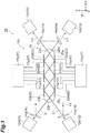
- FIG. 1 is a diagram illustrating an outline of a laser device according to a first embodiment.
- FIG. 2 is a perspective view illustrating a laser medium illustrated in FIG. 1 .
- FIG. 3 is a partially enlarged cross-sectional view of the laser device illustrated in FIG. 1 .
- a laser device 1A includes a laser medium unit 10A, a plurality of (here, four) excitation light source units 12 (excitation light source units 12a, 12b, 12c, and 12d) which supply excitation light L1, and a plurality of (here, four) mirror portions 14 (mirror portions 14a, 14b, 14c, and 14d) which reflect laser light L2 corresponding to light (seed light) to be amplified.
- excitation light source units 12a, 12b, 12c, and 12d which supply excitation light L1
- mirror portions 14 mirror portions 14a, 14b, 14c, and 14d
- the laser medium unit 10A includes a slab laser medium 16, a container (not illustrated) which accommodates the laser medium 16, a cooling member 17, and a plurality of heating members 18.
- the heating member 18 is not illustrated in FIGS. 1 and 2 .
- the laser medium 16 includes an optical medium 20, a plurality of (here, six) plate-shaped laser gain media 22 (laser gain media 22a, 22b, 22c, 22d, 22e, and 22f), and a plurality of reflection members 23 (see FIG. 3 ).
- the laser gain media 22 are respectively bonded to the optical media 20.
- the optical medium 20 is a thin flat plate having a hexagonal column shape and includes six flat side surfaces 20a, 20b, 20c, 20d, 20e, and 20f.
- the dimensions of the optical medium 20 in the X-axis direction, the Y-axis direction, and the Z-axis direction are about 100 mm, 15 mm, and 30 mm.
- the side surfaces 20a and 20b have the same shape and the side surfaces 20c to 20f have the same shape.
- the side surface 20b is parallel to the side surface 20a and is located on the side opposite to the side surface 20a and the side surface 20e is parallel to the side surface 20c and is located on the side opposite to the side surface 20c.
- the side surface 20f is parallel to the side surface 20d and is located on the side opposite to the side surface 20d.
- the optical medium 20 can be symmetric with respect to an imaginary plane which is parallel to the side surface 20a (or the side surface 20b) and is located at the center between the side surface 20a and the side surface 20b in the normal direction of the side surface 20a.
- the optical medium 20 is, for example, a transparent member formed of yttrium-aluminum garnet (YAG).
- YAG yttrium-aluminum garnet
- an active element such as Nd is not added to the optical medium 20.
- the excitation light L1 and the laser light L2 can be transmitted through the optical medium 20.
- FIG. 3 representatively illustrates a portion corresponding to one laser gain medium 22.
- the laser gain medium 22 has a rectangular plate shape.
- the Y-axis direction is set as the thickness direction of the laser gain medium 22 and the X-axis direction and the Z-axis direction are set as the extension direction of the laser gain medium 22 (a direction along the plate surface).
- the dimension of the laser gain medium 22 in the extension direction is larger than an irradiation area (an irradiation area IR to be described later) of the incident excitation light L1.
- the laser gain medium 22 is, for example, YAG doped with Nd as an active element. That is, an active element is added to the laser gain medium.
- the laser gain medium 22 is excited by the excitation light L1 so as to output emission light.
- An example of the emission light is stimulated emission light. This stimulated emission light contributes to the light amplification of the laser light L2.
- the laser gain media 22a to 22c are bonded to the side surface 20a of the optical medium 20 and the laser gain media 22d to 22f are bonded to the side surface 20b.
- the laser gain medium 22 can be bonded to the optical medium 20 by, for example, a ceramic composite technique.
- the side surfaces 20c, 20d, 20e, and 20f to which the laser gain medium 22 is not bonded among the side surfaces 20a to 20f of the optical medium 20 are input/output surfaces where at least one of the excitation light L1 and the laser light L2 is incident and emitted.
- the excitation light source units 12 respectively output the excitation light L1 incident from the side surfaces 20c, 20d, 20e, and 20f.
- the excitation light source unit 12 includes an excitation light source such as a semiconductor laser (for example, a laser diode) outputting light of a wavelength capable of exciting the laser gain medium 22.
- the excitation light source unit 12 may include a condensing optical system that condenses the excitation light L1 output from the excitation light source.
- the mirror portions 14 are disposed on the optical path of the excitation light L1 from the excitation light source units 12 so as to be located between the side surfaces 20c to 20f and the excitation light source units 12 corresponding to the side surfaces 20c to 20f.
- the mirror portion 14 allows the excitation light L1 to be transmitted therethrough and allows the laser light L2 to be fully reflected therefrom.
- the mirror portion 14a reflects the laser light L2 and allows the laser light L2 to be incident from the side surface 20c to the optical medium 20.
- the laser light L2 can be, for example, light output from a laser light source such as a fiber laser.
- the laser light L2 is incident from a direction different from the axial direction of the optical path of the excitation light L1 from the excitation light source unit 12a into the mirror portion 14a.
- the mirror portion 14a is disposed to reflect the laser light L2 so that the laser light L2 is propagated through the optical medium 20 by the optical path coaxial with the optical path of the excitation light L1 output from the excitation light source unit 12a.
- the laser light L2 reflected by the mirror portion 14a is parallel to the excitation light L1, but this is a convenience for specifying the laser light L2.
- the parallel arrangement of the excitation light L1 and the laser light L2 indicates a coaxial state thereof.
- the mirror portions 14b and 14c are disposed so that the laser light L2 emitted from the side surface 20d of the optical medium 20 is incident to the optical medium 20 again in a direction coaxial with the optical path of the excitation light L1 from the excitation light source unit 12c.
- the mirror portion 14d is disposed to reflect the laser light L2 emitted from the side surface 20f in a direction different from the axial direction of the optical path of the excitation light L1 from the excitation light source unit 12d.
- the excitation light L1 output from the excitation light source unit 12 is transmitted through the mirror portion 14 and is incident from the corresponding side surfaces 20c to 20f to the optical medium 20.
- the excitation light L1 which is incident to the optical medium 20 is reflected by the reflection member 23 in a second surface S2 of the laser gain medium 22 so that the excitation light is propagated through the optical medium 20 in a zigzag shape and is emitted from the side surfaces 20c to 20f.
- the excitation light L1 which is incident from the side surface 20c passes through the laser gain media 22f, 22b, and 22d in order of the laser gain medium 22f, the laser gain medium 22b, and the laser gain medium 22d so as to be emitted from the side surface 20d.
- the excitation light L1 which is incident from the side surface 20d passes through the laser gain media 22d, 22b, and 22f in order of the laser gain medium 22d, the laser gain medium 22b, and the laser gain medium 22f so as to be emitted from the side surface 20c.
- the paths of the excitation lights L1 respectively input from the side surfaces 20c and 20d can be set to opposite directions.
- the excitation light L1 which is incident from the side surface 20e passes through the laser gain media 22c, 22e, and 22a in order of the laser gain medium 22c, the laser gain medium 22e, and the laser gain medium 22a so as to be emitted from the side surface 20f.
- the excitation light L1 which is incident from the side surface 20f passes through the laser gain media 22a, 22e, and 22c in order of the laser gain medium 22a, the laser gain medium 22e, and the laser gain medium 22c so as to be emitted from the side surface 20e.
- the paths of the excitation lights L1 respectively input from the side surfaces 20e and 20f can be set to opposite directions.
- a part of the excitation light L1 excites the laser gain medium 22 while being absorbed to the laser gain medium 22 during the propagation inside the optical medium 20.
- a perpendicular incidence can be exemplified.
- the excitation light L1 may be obliquely incident from the excitation light source unit 12 to the side surfaces 20c to 20f.
- the incidence angle of the excitation light L1 with respect to the side surfaces 20c to 20f can be set to a degree that the axis of the optical path of the excitation light L1 propagated in the opposite direction slightly deviates inside the optical medium 20. Accordingly, when the optical path of certain excitation light (referred to as reference excitation light) slightly deviates from the optical path of the counter excitation light with respect to that excitation light inside the optical medium 20 and the light is emitted from the side surfaces 20c to 20f, the incidence direction of the reference excitation light largely deviates from the emission direction of the counter excitation light. As a result, it is possible to prevent the counter excitation light from being incident to the excitation light source outputting the reference excitation light in the excitation light source unit 12.
- reference excitation light slightly deviates from the optical path of the counter excitation light with respect to that excitation light inside the optical medium 20 and the light is emitted from the side surfaces 20c to 20f
- the laser light L2 which is supplied from the laser light source unit is reflected by the mirror portion 14a and is incident from the side surface 20c into the optical medium 20 in a direction coaxial with the excitation light L1 from the excitation light source unit 12a.
- the laser light L2 which is seed light incident from the side surface 20c passes through the same optical path as that of the excitation light L1 so as to be emitted from the side surface 20d.
- the light which is emitted from the side surface 20d is reflected in order of the mirror portions 14b and 14c and is incident from the side surface 20e into the optical medium 20 again in a direction coaxial with the excitation light L1 from the excitation light source unit 12c.
- the laser light L2 which is incident from the side surface 20e into the optical medium 20 passes through the same optical path as that of the excitation light L1 from the excitation light source unit 12c so as to be emitted from the side surface 20f.
- the laser light L2 When the laser light L2 is incident to the laser gain medium 22 excited by the excitation light L1, the laser light L2 is amplified by the emission light according to a stimulated emission phenomenon. For that reason, since the laser light L2 is propagated through the optical medium 20 while being incident in order of the laser gain media 22a to 22f in a zigzag shape, the amplified laser light L2 is emitted from the side surface 20f. The laser light L2 emitted from the side surface 20f is reflected by the mirror portion 14d and is extracted as output light from the laser device 1A.
- the laser gain medium 22 is irradiated with the excitation light L1 and the laser light L2 through the optical medium 20.
- the laser gain medium 22 includes a first surface S1 and a second surface S2 intersecting (being orthogonal to) the thickness direction (the Y-axis direction) and a third surface S3 along the thickness direction.
- the thickness of the laser gain medium 22 which is defined as a distance between the first surface S1 and the second surface S2 is, for example, about 0.25 mm or more and 10 mm or less.
- the first surface S1 is a surface bonded to the optical medium 20 and is an input/output surface of the excitation light L1 and the laser light L2. That is, the laser gain medium 22 generates the emission light by the irradiation of the excitation light L1 from the first surface S1.
- the second surface S2 is a surface opposite to the first surface S1.
- the reflection member 23 is provided on the second surface S2. Here, the reflection member 23 covers the entirety of the second surface S2.
- the reflection member 23 is, for example, a high-reflection coating (for example, a reflection film) having high reflectivity with respect to at least two wavelengths of the excitation light L1 and the laser light L2.
- the wavelength of the excitation light L1 is 808 nm and the wavelength of the laser light L2 is 1064 nm. Accordingly, as described above, the excitation light L1 and the laser light L2 are reflected by the reflection member 23 in the second surface S2.
- the third surface S3 is a surface which is located at the outer edge portion of the laser gain medium 22 so as to connect the first surface S1 and the second surface S2, that is, a side end surface.
- the laser gain medium 22 includes the irradiation area IR which is irradiated with the excitation light L1 and an outer area OR which is located on the outside of the irradiation area IR when viewed from the thickness direction.
- the laser gain medium 22 consists of the irradiation area IR and the annular outer area OR which surrounds the irradiation area IR.
- the excitation light L1 is obliquely incident to the laser gain medium 22 (the first surface S1) (that is, so as to be inclined with respect to the normal line of the first surface S1)
- the irradiation area IR of the excitation light L1 has an oval shape as illustrated in FIG. 4(a).
- FIG. 4(b) is an example of an intensity distribution of the excitation light L1 in the irradiation area IR.
- the irradiation area IR is also an excitation area which is excited by the irradiation of the excitation light L1 in the laser gain medium 22. Further, the irradiation area IR is also a heating area which is heated by the irradiation of the excitation light L1. Meanwhile, the outer area OR is also a non-excitation area and a non-heating area.
- the laser light source unit, the excitation light source unit 12, and the mirror portion 14 constitute an input optical system for inputting the excitation light L1 and the laser light L2 to be amplified from the first surface S1 to the laser gain medium 22. More specifically, here, the input optical system including the laser light source unit, the excitation light source unit 12, and the mirror portion 14 inputs the laser light L2 and the excitation light L1 from the first surface S1 to the laser gain medium 22 through the optical medium 20 by the coaxial optical path.
- the cooling member 17 cools each laser gain medium 22.
- the cooling member 17 includes a contact portion 17a which contacts the laser gain medium 22 through the reflection member 23 and a cooling unit 17b which is connected to the contact portion 17a.
- the contact portion 17a provides a heat transfer path between the laser gain medium 22 and the cooling unit 17b.
- the contact portion 17a is, for example, a heat pipe.
- the contact portion 17a is provided in each laser gain medium 22.
- the cooling unit 17b can store, for example, a liquefied gas (for example, liquid nitrogen) as a heat medium (refrigerant). Further, the cooling unit 17b is, for example, a cooling device such as a refrigerator. Additionally, FIG. 1 illustrates an example in which six contact portions 17a are distributed to two cooling units 17b, but the contact portions may be integrated in one cooling unit 17b.
- the contact portion 17a is thermally connected to the second surface S2 of the laser gain medium 22 through the reflection member 23 so that a cooling area CA of the laser gain medium 22 is formed on the second surface S2.
- the cooling area CA is an area in which the cooling member 17 contacts the second surface S2 through the reflection member 23.
- the cooling area CA corresponds to an end surface on the side of the second surface S2 of the contact portion 17a.
- the outer edge of the cooling area CA is located within the irradiation area IR when viewed form the thickness direction (the Y-axis direction) of the laser gain medium 22.
- a case in which the outer edge of the cooling area CA is located within the irradiation area IR includes a case in which the outer edge of the cooling area CA matches the outer edge of the irradiation area IR and a case in which the outer edge of the cooling area CA is located on the inside (the center side of the irradiation area IR) in relation to the outer edge of the irradiation area IR, when viewed from the thickness direction of the laser gain medium 22.
- the outer edge of the cooling area CA is located on the inside of the outer edge of the irradiation area IR when viewed from the thickness direction of the laser gain medium 22. For this reason, the cooling member 17 cools the laser gain medium 22 by exchanging heat with the laser gain medium 22 in a range narrower than the irradiation area IR on the second surface S2.
- an annular non-cooling area TA is formed on the outside of the cooling area CA.
- the non-cooling area TA of the second surface S2 is exposed to, for example, an atmosphere in a container. Accordingly, in the non-cooling area TA, the laser gain medium 22 is substantially insulated without any heat exchange with the other members.
- the heating member 18 is for heating the laser gain medium 22.
- the heating member 18 is provided in each laser gain medium 22. More specifically, the heating member 18 is provided on a surface other than the first surface S1 at the outer edge portion in the extension direction of the laser gain medium 22 and heats the laser gain medium 22 by inputting heat to the outer area OR of the laser gain medium 22.
- the heating member 18 is formed in an annular shape and is provided on the third surface S3 of the laser gain medium 22.
- the heating member 18 is, for example, a ring heater. Additionally, the heating member 18 may be formed on, for example, the second surface S2 at the outer edge portion of the laser gain medium 22 by printing, adhering, or attaching.
- FIG. 5 is a diagram showing a result obtained by calculating the phase shift amount of the laser gain medium.
- FIGS. 5(a) and 5(c) are diagrams showing a temperature distribution within a cross-section taken along the thickness direction of the laser gain medium. In the drawings below, in the case of showing the temperature distribution, the temperature becomes higher as the light gray changes to the dark gray. Further, FIGS. 5(b) and 5(d) are graphs showing a relationship between the phase shift amount and the radial position of the laser gain medium.
- the phase shift amount is a value obtained when the laser light is input and output in a direction parallel to the thickness direction of the laser gain medium (in a direction perpendicular to the incident surface).
- the laser gain medium is formed in a disk shape for convenience of description. For this reason, since the laser gain medium is symmetric with respect to the center line of the radial direction, a range of a half in the radial direction is shown below.
- the thickness of the laser gain medium is set to 0.25 mm and the radius is set to 10 mm.
- the irradiation area (the excitation area) of the excitation light in the laser gain medium is formed in a disk shape having a radius of 5 mm and concentric with the laser gain medium. That is, here, the irradiation area is set to a range of 50% of the radial position from the center of the laser gain medium in the radial direction.
- FIGS. 5(a) and 5(b) show a case in which the entirety of the second surface of the laser gain medium (the surface opposite to the incident surface of the excitation light) is set as the cooling area (hereinafter, also referred to as cooling of 100%).
- FIGS. 5(c) and 5(d) show a case in which a range of 50% of the radial position from the center of the second surface in the radial direction is set as the cooling area (hereinafter, also referred to as cooling of 50%). That is, in FIGS. 5(c) and 5(d) , the outer edge of the cooling area matches the outer edge of the irradiation area.
- the temperature of the outer area outside the irradiation area increases in the case of the cooling of 50% as compared with the case of the cooling of 100%.
- the phase shift amount of the outer area is uniform in the radial direction and a difference with the phase shift amount in the irradiation area decreases. That is, when the thickness of the laser gain medium is uniform, it is understood that an influence (a thermal lensing effect) on the incident light due to a difference in phase shift amount occurring in a boundary area between the irradiation area (the excitation area) and the outer area (the non-excitation area) can be reduced in the case of the cooling of 50% as compared with the cooling of 100%.
- FIG. 6(a) is a graph showing a calculation result of a relationship between the laser gain medium and the thermal lensing effect.
- the thermal lensing effect can be reduced to about 1/50 of the reference value even when the thickness of the laser gain medium is thickened to 5 mm.
- FIG. 6(b) is a graph showing a calculation result of a change of the phase shift amount depending on the heating of the laser gain medium by the heating member.
- a dashed line indicates a heating case and a solid line indicates a non-heating case.
- heat is input from the third surface (the side end surface) of the laser gain medium.
- FIG. 6(b) in a case where heating exists, it is understood that since a heating the irradiation area by incidence of the excitation light and an influence of heat inputting to the outer area from the third surface are added, a difference of phase shift (that is, the thermal lensing effect) is reduced as the whole.
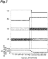
- FIG. 7 is a diagram showing a calculation result when the outer edge of the cooling area is located on the inside in relation to the irradiation area. That is, FIG. 7 shows a case in which the laser gain medium is cooled from a range narrower than the irradiation area in the second surface.
- the thickness of the laser gain medium is set to 0.25 mm.
- the irradiation area is set to a range of 50% of the radial position and the cooling area is set to 43% of the radial position so that a difference is formed between the irradiation area and the cooling area.
- FIG. 7(a) shows a range of the cooling area in the radial direction
- FIG. 7(b) shows a range of the irradiation area of the excitation light in the radial direction
- FIG. 7(c) shows a range of the irradiation area in the radial direction within a cross-section taken along the thickness direction.
- FIG. 7(d) shows a temperature distribution within a cross-section taken along the thickness direction
- FIG. 7(e) shows a phase shift amount with respect to the radial position.
- an outer area that is, a range from 43% to 50% of the radial position
- a temperature distribution of a mismatched portion between excitation and cooling has a shape in which the heat flow in the thickness direction and the heat flow in the radial direction are mixed.
- the temperature of the outer area becomes higher than that of the irradiation area (the heating area) and the phase shift amount of the outer area becomes larger than the phase shift amount of the irradiation area.
- a thermal barrier which is generated by the mismatch between heating and cooling can increase the temperature of the outer area or the thermally induced phase shift to be larger than those of the irradiation area. Also in that case, it is understood that the distribution of the phase shift is uniform. Thus, it is considered that a difference in phase shift amount in a boundary between the irradiation area and the outer area can be reduced as much as possible by controlling the phase of the outer area using this principle.
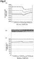
- FIG. 8(a) is a graph showing a calculation result for optimizing the cooling area.
- the thickness of the laser gain medium is set to 2 mm and the irradiation area is set to a range of 50% of the radial position.
- a case (cooling of 47%) in which the cooling area is set to a range of 47% of the radial position is indicated by a solid line
- a case (cooling of 46%) in which the cooling area is set to a range of 46% of the radial position is indicated by a dashed line
- a case (cooling of 45%) in which the cooling area is set to a range of 45% of the radial position is indicated by a one-dotted chain line.
- the phase shift amount of the outer area becomes smaller than the phase shift amount of the irradiation area.
- the phase shift amount of the outer area becomes larger than the phase shift amount of the irradiation area.
- the phase shift amount of the outer area becomes substantially the same as the phase shift amount of the irradiation area.
- FIGS. 8(b) and 8(c) show a result for optimizing the cooling area in a state in which the thickness of the laser gain medium is 0.5 mm.
- FIG. 8(b) shows a temperature distribution within a cross-section taken along the thickness direction
- FIG. 8(c) shows a phase shift amount with respect to a radial position.
- the cooling area is set to a range of 49% of the radial position.
- FIG. 9 is a graph of summarizing the calculation results of FIGS. 5 to 8 .
- a vertical axis indicates a normalized thermal lensing effect.
- the thermal lensing effect can be reduced most when the cooling area is optimized in a range within the irradiation area (here, a range within 50%) and heating is performed from the outer area. In this case, it is possible to reduce the thermal lensing effect to 1/1000 or less in a wide range in which the thickness of the laser gain medium is 0.25 mm to 5 mm.
- the plate-shaped laser gain medium 22 includes the first surface S1 which is an incident surface of the excitation light L1 and the second surface S2 which is a surface opposite to the first surface S1 and is provided with the cooling area CA of the cooling member 17. Further, the laser gain medium 22 includes the irradiation area IR which is irradiated with the excitation light L1 and the outer area OR which is located on the outside of the irradiation area IR when viewed from the thickness direction.
- the outer edge of the cooling area CA is located within the irradiation area IR of the excitation light L1 when viewed from the thickness direction. That is, in this laser medium unit 10A, the cooling area CA becomes a range equal to or smaller than the irradiation area IR of the excitation light L1 when viewed from the thickness direction of the laser gain medium 22.
- this laser medium unit 10A it is possible to reduce the thermal lensing effect and to improve the beam quality.
- the laser medium unit 10A further includes the heating member 18 for heating the laser gain medium 22.
- the heating member 18 is provided on a surface other than the first surface S1 in the outer edge portion of the laser gain medium 22 and heats the laser gain medium 22 by inputting heat to the outer area OR.
- the laser gain medium 22 includes the third surface S3 which is located on the side of the outer edge portion and connects the first surface S1 and the second surface S2 along the thickness direction. Then, the heating member 18 may be provided on the third surface S3. In this way, the heating member can be provided on the third surface S3 corresponding to the side end surface of the laser gain medium 22.
- the laser device 1A includes the laser medium unit 10A and an input optical system for inputting the excitation light L1 and the laser light L2 to be amplified from the first surface S1 to the laser gain medium 22.
- this laser device 1A it is possible to reduce the thermal lensing effect of the laser gain medium 22 and to improve the beam quality.
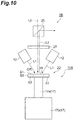
- FIG. 10 is a diagram schematically illustrating the laser device according to the second embodiment.
- a laser device 1B includes the laser medium unit 10A, the pair of excitation light source units 12, a polarizing beam splitter 25, and a polarizing rotating element 27.
- the polarizing rotating element 27 is, for example, a ⁇ /4 wavelength plate.
- the laser medium unit 10A includes a single laser gain medium 22, along with the cooling member 17, the heating member 18, and the reflection member 23 corresponding thereto. Further, the laser medium unit 10A does not include the optical medium 20.
- the laser light L2 which is seed light to be amplified is emitted from a laser light source unit (not illustrated), is transmitted through the polarizing beam splitter 25 and the polarizing rotating element 27 in a linear polarized state, and is incident from the first surface S1 to the laser gain medium 22.
- the laser light L2 is incident to the laser gain medium 22 in the thickness direction of the laser gain medium 22, that is, in a direction perpendicular to the first surface S1.
- the excitation light L1 is incident from the first surface S1 to the laser gain medium 22 through the optical path inclined with respect to the normal line of the first surface S1 by the pair of excitation light source units 12.
- the laser light source unit, the polarizing beam splitter 25, the polarizing rotating element 27, and the excitation light source unit 12 constitute an input optical system which inputs the excitation light L1 and the laser light L2 to be amplified from the first surface S1 to the laser gain medium 22. More specifically, here, the input optical system inputs the laser light L2 and the excitation light L1 from the first surface S1 to the laser gain medium 22 through different optical paths.
- the laser light L2 which is incident to the laser gain medium 22 is amplified inside the laser gain medium 22 and is reflected by the reflection member 23 in the second surface S2.
- the laser light L2 reflected in the second surface S2 is further amplified inside the laser gain medium 22 and is emitted from the laser gain medium 22 in the first surface S1.
- the laser light L2 emitted from the laser gain medium 22 is transmitted through the polarizing rotating element 27 so that the polarizing direction thereof rotates by 90°.
- the laser light L2 transmitted through the polarizing rotating element 27 is reflected in a direction different from the incident light in the polarizing beam splitter 25 and is output to the outside.
- the laser device 1B and the laser medium unit 10A with the above-described configuration it is possible to reduce the thermal lensing effect and to improve the beam quality due to the same reason as described above.
- FIG. 11 is a diagram schematically illustrating the laser device according to the third embodiment.
- a laser device 1C includes the laser medium unit 10A similar to that of the second embodiment and the pair of excitation light source units 12.
- the laser light L2 which is seed light to be amplified is emitted from a laser light source unit (not illustrated) and is incident from the first surface S1 to the laser gain medium 22.
- the laser light L2 is incident to the laser gain medium 22 by the optical path inclined with respect to the normal line of the first surface S1 by a predetermined angle.
- the laser light L2 corresponding to the incident light and the laser light L2 corresponding to the emission light are spatially divided.
- the excitation light L1 is incident from the first surface S1 to the laser gain medium 22 through the optical path inclined by a different predetermined angle with respect to the normal line of the first surface S1 by the pair of excitation light source units 12.
- the laser light source unit and the excitation light source unit 12 constitute an input optical system which inputs the excitation light L1 and the laser light L2 to be amplified from the first surface S1 to the laser gain medium 22. More specifically, here, the input optical system inputs the laser light L2 and the excitation light L1 from the first surface S1 to the laser gain medium 22 by different optical paths.
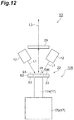
- FIG. 12 is a diagram schematically illustrating the laser device according to the fourth embodiment.
- a laser device 1D includes the laser medium unit 10A similar to that of the second embodiment, the pair of excitation light source units 12, and a resonator mirror 29.
- the resonator mirror 29 constitutes a laser resonator between the resonator mirror 29 and the reflection member 23 on the second surface S2 of the laser gain medium 22.
- the laser device (the laser oscillator) 1D generates laser light L3 by supplying the excitation light L1 to the laser gain medium 22 of the laser medium unit 10A.
- the resonator mirror 29 partially reflects the laser light L3.
- the resonator mirror 29 constitutes an optical resonator along with the reflection member 23.
- the resonator mirror 29 and the reflection member 23 are disposed so that the laser light L3 is repeatedly reflected between the resonator mirror 29 and the reflection member 23 and the laser gain medium 22 is disposed within the resonant light path of the laser light L3 between the resonator mirror 29 and the reflection member 23.
- the excitation light L1 output from the excitation light source unit 12 excites the laser gain medium 22 similarly to the case of the laser device (the laser amplifier) 1B.
- the laser light L3 which is the emission light from the excited laser gain medium 22 is reflected between the resonator mirror 29 and the reflection member 23 and is optically amplified.
- the laser light L3 partially transmitted through the resonator mirror 29 is light output from the laser oscillator.
- the laser medium unit and the laser device according to an aspect of the invention are not limited to the laser medium unit 10A and the laser devices 1A to 1D described above.
- the laser medium unit and the laser device according to an aspect of the invention can be obtained by arbitrarily modifying the laser medium unit 10A and the laser devices 1A to 1D without changing the spirit of claims.
- the laser devices 1A to 1D are not limited to the configurations illustrated in the drawings and may be configured as different laser devices by replacing or adding partial components. Further, the laser device may be appropriately modified in accordance with the wavelengths of the excitation light L1 and the laser lights L2 and L3 or the materials of the optical medium 20 and the laser gain medium 22.
- the materials of the optical medium 20 and the laser gain medium 22 are not limited to YAG and the active element added to the laser gain medium 22 is not limited to Nd.
- the optical material and the active element used in a solid laser device such as a laser amplifier or a laser oscillator may be used.
- GGG Gadolinium Gallium Garnet (Gd 3 Ga 5 O 12 )
- Yb Gadolinium Gallium Garnet
- the laser gain medium 22 is not limited to a rectangular plate shape and may be a disk shape or other plate shapes.
- the cooling member 17 is not limited thereto and may be, for example, another one such as a Peltier element provided in each of the laser gain media 22.
- a laser medium unit and a laser device capable of improving beam quality can be provided.
- 1A to 1D laser device, 10A: laser medium unit, 12: excitation light source unit, 16: laser medium, 17: cooling member, 18: heating member, 20: optical medium, 22: laser gain medium, 23: reflection member, 25: polarizing beam splitter, 27: polarizing rotating element, 29: resonator mirror, S1: first surface, S2: second surface, S3: third surface, L1: excitation light, L2: laser light, L3: laser light, IR: irradiation area, OR: outer area, CA: cooling area, TA: non-cooling area.
Landscapes
- Physics & Mathematics (AREA)
- Electromagnetism (AREA)
- Engineering & Computer Science (AREA)
- Plasma & Fusion (AREA)
- Optics & Photonics (AREA)
- Chemical & Material Sciences (AREA)
- Crystallography & Structural Chemistry (AREA)
- Lasers (AREA)
- Semiconductor Lasers (AREA)
Abstract
Description
- An aspect of the present invention relates to a laser medium unit and a laser device.
-
Patent Literature 1 describes a laser medium unit. This laser medium unit includes a laser medium in which a plurality of plate-shaped laser gain media generating emission light by the irradiation of excitation light are bonded to an optical medium allowing both of the excitation light and the emission light to be transmitted therethrough. Further, this laser medium unit includes a container which accommodates the laser medium and has a cooling medium passage for cooling the laser gain medium. - Patent Literature 1: Japanese Patent Application No.
2015-167216 - In the laser medium unit described in
Patent Literature 1, the laser gain medium has a rectangular plate shape as an example. Then, in the laser gain medium, one surface of a pair of surfaces intersecting each other in the thickness direction is bonded to the optical medium so as to be used as an input/output surface of the excitation light and the emission light and the entirety of the other surface is in contact with the cooling medium passage so as to be used for a cooling operation. Particularly, in this laser medium unit, a cross-sectional area of the cooling medium passage is adjusted to control a flow rate of a cooling medium inside the cooling medium passage so that the temperature uniformity of the laser gain medium is improved. That is, in the above-described technical field, it is preferable to reduce a thermal lensing effect due to a temperature gradient in order to improve beam quality. - Here, an aspect of the invention is to provide a laser medium unit and a laser device capable of improving beam quality.
- In order to solve the above-described problems, the inventor has conducted a careful examination and found knowledge that a thermal lensing effect can be reduced by controlling a relative relationship between an irradiation area of excitation light in a laser gain medium and a cooling area provided to cool the laser gain medium. That is, the inventor has found that a thermal lensing effect can be reduced as compared with a case in which a range wider than the irradiation area is cooled by setting the cooling area to be equal to or smaller than the irradiation area of the excitation light. An aspect of the invention is obtained on the basis of the knowledge.
- That is, a laser medium unit according to an aspect of the invention includes: a plate-shaped laser gain medium which includes a first surface and a second surface opposite to the first surface and generates emission light by the irradiation of excitation light from the first surface; a reflection member that is provided on the second surface so as to reflect the excitation light and the emission light; and a cooling member that cools the laser gain medium, in which the laser gain medium includes an irradiation area which is irradiated with the excitation light and an outer area which is located outside the irradiation area when viewed from a thickness direction intersecting the first surface and the second surface, in which the cooling member is thermally connected to the second surface through the reflection member so that a cooling area of the laser gain medium is formed on the second surface, and in which an outer edge of the cooling area is located inside the irradiation area when viewed from the thickness direction.
- In this laser medium unit, the plate-shaped laser gain medium includes the first surface which is the incident surface of the excitation light and the second surface which is the surface opposite to the first surface and is provided with the cooling area of the cooling member. Further, the laser gain medium includes the irradiation area which is irradiated with the excitation light and the outer area which is located on the outside of the irradiation area when viewed from the thickness direction. Then, the outer edge of the cooling area is located inside the irradiation area of the excitation light when viewed from the thickness direction. That is, in this laser medium unit, the cooling area is set to be equal to or smaller than the irradiation area of the excitation light when viewed from the thickness direction of the laser gain medium. Thus, according to this laser medium unit, it is possible to reduce the thermal lensing effect and to improve the beam quality. Additionally, the cooling area indicates, for example, an area in which the cooling member and the second surface are in contact through the reflection member.
- The laser medium unit according to an aspect of the invention may further include a heating member that heats the laser gain medium and the heating member may be provided on a surface other than the first surface in an outer edge portion of the laser gain medium and heats the laser gain medium by inputting heat to the outer area. By using such a heating member, it is possible to further reduce the thermal lensing effect without disturbing the incidence of the excitation light on the first surface.
- In the laser medium unit according to an aspect of the invention, the laser gain medium may include a third surface which is located on the side of the outer edge portion and connects the first surface and the second surface in the thickness direction and the heating member may be provided on the third surface. In this way, the heating member can be provided on the third surface which is the side end surface of the laser gain medium.
- A laser device according to an aspect of the invention includes the above-described laser medium unit and an input optical system which inputs the excitation light and the laser light to be amplified from the first surface to the laser gain medium. This laser device includes the above-described laser medium unit. Thus, according to this laser device, it is possible to reduce the thermal lensing effect of the laser gain medium and to improve the beam quality.
- The laser device according to an aspect of the invention may further include an optical medium to which an active element is not added and through which the excitation light and the laser light are transmittable, the laser gain medium may be provided on the optical medium so that the first surface is bonded to the optical medium, and the input optical system may input the laser light and the excitation light from the first surface to the laser gain medium through the optical medium by the coaxial optical path.
- According to an aspect of the invention, it is possible to provide a laser medium unit and a laser device capable of improving beam quality.
-
-
FIG. 1 is a diagram illustrating an outline of a laser device according to a first embodiment. -
FIG. 2 is a perspective view illustrating a laser medium illustrated inFIG. 1 . -
FIG. 3 is a partially enlarged cross-sectional view of the laser device illustrated inFIG. 1 . -
FIG. 4 is a diagram illustrating a laser gain medium and an excitation light intensity distribution illustrated inFIG. 1 . -
FIG. 5 is a diagram showing a result obtained by calculating a phase shift amount of the laser gain medium. -
FIG. 6 is a graph showing a calculation result of a relationship between the laser gain medium and a thermal lensing effect and is a graph showing a calculation result of a change of a phase shift amount depending on the heating of the laser gain medium by a heating member. -
FIG. 7 is a diagram showing a calculation result in a case in which an outer edge of a cooling area is located on the inside in relation to an irradiation area. -
FIG. 8 is a diagram showing a calculation result for optimizing the cooling area. -
FIG. 9 is a graph summarizing the calculation results ofFIGS. 5 to 8 . -
FIG. 10 is a diagram illustrating an outline of a laser device according to a second embodiment. -
FIG. 11 is a diagram illustrating an outline of a laser device according to a third embodiment. -
FIG. 12 is a diagram illustrating an outline of a laser device according to a fourth embodiment. - Hereinafter, embodiments according to an aspect of the invention will be described in detail with reference to the drawings. Additionally, in the drawings, the same or equivalent components will be denoted by the same reference numerals and a redundant description thereof will be omitted. Further, in the drawings, there is a case where an orthogonal coordinate system S defined by X, Y, and Z axes is illustrated.
-
FIG. 1 is a diagram illustrating an outline of a laser device according to a first embodiment.FIG. 2 is a perspective view illustrating a laser medium illustrated inFIG. 1 .FIG. 3 is a partially enlarged cross-sectional view of the laser device illustrated inFIG. 1 . As illustrated inFIGS. 1 to 3 , alaser device 1A includes alaser medium unit 10A, a plurality of (here, four) excitation light source units 12 (excitationlight source units mirror portions - The
laser medium unit 10A includes aslab laser medium 16, a container (not illustrated) which accommodates thelaser medium 16, acooling member 17, and a plurality ofheating members 18. Here, theheating member 18 is not illustrated inFIGS. 1 and2 . Thelaser medium 16 includes anoptical medium 20, a plurality of (here, six) plate-shaped laser gain media 22 (laser gain media FIG. 3 ). Thelaser gain media 22 are respectively bonded to theoptical media 20. - Here, the
optical medium 20 is a thin flat plate having a hexagonal column shape and includes sixflat side surfaces optical medium 20 in the X-axis direction, the Y-axis direction, and the Z-axis direction are about 100 mm, 15 mm, and 30 mm. Theside surfaces side surfaces 20c to 20f have the same shape. Theside surface 20b is parallel to theside surface 20a and is located on the side opposite to theside surface 20a and theside surface 20e is parallel to theside surface 20c and is located on the side opposite to theside surface 20c. Similarly, theside surface 20f is parallel to theside surface 20d and is located on the side opposite to theside surface 20d. - The side surfaces 20c and 20f which intersect each other respectively intersect the side surfaces 20a and 20b. Similarly, the side surfaces 20d and 20e which intersect each other respectively intersect the side surfaces 20a and 20b. The optical medium 20 can be symmetric with respect to an imaginary plane which is parallel to the
side surface 20a (or theside surface 20b) and is located at the center between theside surface 20a and theside surface 20b in the normal direction of theside surface 20a. - The
optical medium 20 is, for example, a transparent member formed of yttrium-aluminum garnet (YAG). For example, an active element such as Nd is not added to theoptical medium 20. The excitation light L1 and the laser light L2 can be transmitted through theoptical medium 20. - The
laser gain media 22 have the same shape. Thus,FIG. 3 representatively illustrates a portion corresponding to onelaser gain medium 22. As an example, thelaser gain medium 22 has a rectangular plate shape. Here, the Y-axis direction is set as the thickness direction of thelaser gain medium 22 and the X-axis direction and the Z-axis direction are set as the extension direction of the laser gain medium 22 (a direction along the plate surface). The dimension of thelaser gain medium 22 in the extension direction is larger than an irradiation area (an irradiation area IR to be described later) of the incident excitation light L1. - The
laser gain medium 22 is, for example, YAG doped with Nd as an active element. That is, an active element is added to the laser gain medium. Thelaser gain medium 22 is excited by the excitation light L1 so as to output emission light. An example of the emission light is stimulated emission light. This stimulated emission light contributes to the light amplification of the laser light L2. Thelaser gain media 22a to 22c are bonded to theside surface 20a of theoptical medium 20 and thelaser gain media 22d to 22f are bonded to theside surface 20b. The laser gain medium 22 can be bonded to theoptical medium 20 by, for example, a ceramic composite technique. - The side surfaces 20c, 20d, 20e, and 20f to which the
laser gain medium 22 is not bonded among the side surfaces 20a to 20f of the optical medium 20 are input/output surfaces where at least one of the excitation light L1 and the laser light L2 is incident and emitted. The excitationlight source units 12 respectively output the excitation light L1 incident from the side surfaces 20c, 20d, 20e, and 20f. The excitationlight source unit 12 includes an excitation light source such as a semiconductor laser (for example, a laser diode) outputting light of a wavelength capable of exciting thelaser gain medium 22. The excitationlight source unit 12 may include a condensing optical system that condenses the excitation light L1 output from the excitation light source. - The
mirror portions 14 are disposed on the optical path of the excitation light L1 from the excitationlight source units 12 so as to be located between the side surfaces 20c to 20f and the excitationlight source units 12 corresponding to the side surfaces 20c to 20f. Themirror portion 14 allows the excitation light L1 to be transmitted therethrough and allows the laser light L2 to be fully reflected therefrom. In particular, themirror portion 14a reflects the laser light L2 and allows the laser light L2 to be incident from theside surface 20c to theoptical medium 20. The laser light L2 can be, for example, light output from a laser light source such as a fiber laser. The laser light L2 is incident from a direction different from the axial direction of the optical path of the excitation light L1 from the excitationlight source unit 12a into themirror portion 14a. - The
mirror portion 14a is disposed to reflect the laser light L2 so that the laser light L2 is propagated through theoptical medium 20 by the optical path coaxial with the optical path of the excitation light L1 output from the excitationlight source unit 12a. InFIG. 1 , the laser light L2 reflected by themirror portion 14a is parallel to the excitation light L1, but this is a convenience for specifying the laser light L2. Similarly, inFIG. 1 , the parallel arrangement of the excitation light L1 and the laser light L2 indicates a coaxial state thereof. - The
mirror portions side surface 20d of theoptical medium 20 is incident to the optical medium 20 again in a direction coaxial with the optical path of the excitation light L1 from the excitationlight source unit 12c. Themirror portion 14d is disposed to reflect the laser light L2 emitted from theside surface 20f in a direction different from the axial direction of the optical path of the excitation light L1 from the excitationlight source unit 12d. - The excitation light L1 output from the excitation
light source unit 12 is transmitted through themirror portion 14 and is incident from the corresponding side surfaces 20c to 20f to theoptical medium 20. As will be described later, the excitation light L1 which is incident to theoptical medium 20 is reflected by thereflection member 23 in a second surface S2 of thelaser gain medium 22 so that the excitation light is propagated through the optical medium 20 in a zigzag shape and is emitted from the side surfaces 20c to 20f. - Specifically, the excitation light L1 which is incident from the
side surface 20c passes through thelaser gain media laser gain medium 22f, thelaser gain medium 22b, and thelaser gain medium 22d so as to be emitted from theside surface 20d. In contrast, the excitation light L1 which is incident from theside surface 20d passes through thelaser gain media laser gain medium 22d, thelaser gain medium 22b, and the laser gain medium 22f so as to be emitted from theside surface 20c. The paths of the excitation lights L1 respectively input from the side surfaces 20c and 20d can be set to opposite directions. - The excitation light L1 which is incident from the
side surface 20e passes through thelaser gain media laser gain medium 22c, thelaser gain medium 22e, and thelaser gain medium 22a so as to be emitted from theside surface 20f. In contrast, the excitation light L1 which is incident from theside surface 20f passes through thelaser gain media laser gain medium 22a, thelaser gain medium 22e, and thelaser gain medium 22c so as to be emitted from theside surface 20e. The paths of the excitation lights L1 respectively input from the side surfaces 20e and 20f can be set to opposite directions. - A part of the excitation light L1 excites the
laser gain medium 22 while being absorbed to thelaser gain medium 22 during the propagation inside theoptical medium 20. As the incidence of the excitation light L1 from the excitationlight source unit 12 to the side surfaces 20c to 20f, a perpendicular incidence can be exemplified. However, the excitation light L1 may be obliquely incident from the excitationlight source unit 12 to the side surfaces 20c to 20f. - When the excitation light L1 is obliquely incident from the excitation
light source unit 12 to the corresponding side surfaces 20c to 20f, the incidence angle of the excitation light L1 with respect to the side surfaces 20c to 20f can be set to a degree that the axis of the optical path of the excitation light L1 propagated in the opposite direction slightly deviates inside theoptical medium 20. Accordingly, when the optical path of certain excitation light (referred to as reference excitation light) slightly deviates from the optical path of the counter excitation light with respect to that excitation light inside theoptical medium 20 and the light is emitted from the side surfaces 20c to 20f, the incidence direction of the reference excitation light largely deviates from the emission direction of the counter excitation light. As a result, it is possible to prevent the counter excitation light from being incident to the excitation light source outputting the reference excitation light in the excitationlight source unit 12. - The laser light L2 which is supplied from the laser light source unit is reflected by the
mirror portion 14a and is incident from theside surface 20c into the optical medium 20 in a direction coaxial with the excitation light L1 from the excitationlight source unit 12a. The laser light L2 which is seed light incident from theside surface 20c passes through the same optical path as that of the excitation light L1 so as to be emitted from theside surface 20d. The light which is emitted from theside surface 20d is reflected in order of themirror portions side surface 20e into the optical medium 20 again in a direction coaxial with the excitation light L1 from the excitationlight source unit 12c. The laser light L2 which is incident from theside surface 20e into the optical medium 20 passes through the same optical path as that of the excitation light L1 from the excitationlight source unit 12c so as to be emitted from theside surface 20f. - When the laser light L2 is incident to the
laser gain medium 22 excited by the excitation light L1, the laser light L2 is amplified by the emission light according to a stimulated emission phenomenon. For that reason, since the laser light L2 is propagated through the optical medium 20 while being incident in order of thelaser gain media 22a to 22f in a zigzag shape, the amplified laser light L2 is emitted from theside surface 20f. The laser light L2 emitted from theside surface 20f is reflected by themirror portion 14d and is extracted as output light from thelaser device 1A. - In this way, the
laser gain medium 22 is irradiated with the excitation light L1 and the laser light L2 through theoptical medium 20. Particularly, thelaser gain medium 22 includes a first surface S1 and a second surface S2 intersecting (being orthogonal to) the thickness direction (the Y-axis direction) and a third surface S3 along the thickness direction. The thickness of thelaser gain medium 22 which is defined as a distance between the first surface S1 and the second surface S2 is, for example, about 0.25 mm or more and 10 mm or less. - The first surface S1 is a surface bonded to the
optical medium 20 and is an input/output surface of the excitation light L1 and the laser light L2. That is, thelaser gain medium 22 generates the emission light by the irradiation of the excitation light L1 from the first surface S1. The second surface S2 is a surface opposite to the first surface S1. Thereflection member 23 is provided on the second surface S2. Here, thereflection member 23 covers the entirety of the second surface S2. - The
reflection member 23 is, for example, a high-reflection coating (for example, a reflection film) having high reflectivity with respect to at least two wavelengths of the excitation light L1 and the laser light L2. As an example, the wavelength of the excitation light L1 is 808 nm and the wavelength of the laser light L2 is 1064 nm. Accordingly, as described above, the excitation light L1 and the laser light L2 are reflected by thereflection member 23 in the second surface S2. The third surface S3 is a surface which is located at the outer edge portion of thelaser gain medium 22 so as to connect the first surface S1 and the second surface S2, that is, a side end surface. - Here, the
laser gain medium 22 includes the irradiation area IR which is irradiated with the excitation light L1 and an outer area OR which is located on the outside of the irradiation area IR when viewed from the thickness direction. Here, thelaser gain medium 22 consists of the irradiation area IR and the annular outer area OR which surrounds the irradiation area IR. Here, since the excitation light L1 is obliquely incident to the laser gain medium 22 (the first surface S1) (that is, so as to be inclined with respect to the normal line of the first surface S1), the irradiation area IR of the excitation light L1 has an oval shape as illustrated inFIG. 4(a). FIG. 4(b) is an example of an intensity distribution of the excitation light L1 in the irradiation area IR. - Additionally, the irradiation area IR is also an excitation area which is excited by the irradiation of the excitation light L1 in the
laser gain medium 22. Further, the irradiation area IR is also a heating area which is heated by the irradiation of the excitation light L1. Meanwhile, the outer area OR is also a non-excitation area and a non-heating area. - As described above, the laser light source unit, the excitation
light source unit 12, and themirror portion 14 constitute an input optical system for inputting the excitation light L1 and the laser light L2 to be amplified from the first surface S1 to thelaser gain medium 22. More specifically, here, the input optical system including the laser light source unit, the excitationlight source unit 12, and themirror portion 14 inputs the laser light L2 and the excitation light L1 from the first surface S1 to thelaser gain medium 22 through theoptical medium 20 by the coaxial optical path. -
FIGS. 1 to 4 will be referred continuously. The coolingmember 17 cools eachlaser gain medium 22. The coolingmember 17 includes acontact portion 17a which contacts thelaser gain medium 22 through thereflection member 23 and acooling unit 17b which is connected to thecontact portion 17a. Thecontact portion 17a provides a heat transfer path between thelaser gain medium 22 and thecooling unit 17b. Thecontact portion 17a is, for example, a heat pipe. - The
contact portion 17a is provided in eachlaser gain medium 22. Thecooling unit 17b can store, for example, a liquefied gas (for example, liquid nitrogen) as a heat medium (refrigerant). Further, thecooling unit 17b is, for example, a cooling device such as a refrigerator. Additionally,FIG. 1 illustrates an example in which sixcontact portions 17a are distributed to two coolingunits 17b, but the contact portions may be integrated in onecooling unit 17b. - The
contact portion 17a is thermally connected to the second surface S2 of thelaser gain medium 22 through thereflection member 23 so that a cooling area CA of thelaser gain medium 22 is formed on the second surface S2. The cooling area CA is an area in which the coolingmember 17 contacts the second surface S2 through thereflection member 23. Here, the cooling area CA corresponds to an end surface on the side of the second surface S2 of thecontact portion 17a. The outer edge of the cooling area CA is located within the irradiation area IR when viewed form the thickness direction (the Y-axis direction) of thelaser gain medium 22. - A case in which the outer edge of the cooling area CA is located within the irradiation area IR includes a case in which the outer edge of the cooling area CA matches the outer edge of the irradiation area IR and a case in which the outer edge of the cooling area CA is located on the inside (the center side of the irradiation area IR) in relation to the outer edge of the irradiation area IR, when viewed from the thickness direction of the
laser gain medium 22. Here, as an example, the outer edge of the cooling area CA is located on the inside of the outer edge of the irradiation area IR when viewed from the thickness direction of thelaser gain medium 22. For this reason, the coolingmember 17 cools thelaser gain medium 22 by exchanging heat with thelaser gain medium 22 in a range narrower than the irradiation area IR on the second surface S2. - In other words, in the second surface S2 of the
laser gain medium 22, an annular non-cooling area TA is formed on the outside of the cooling area CA. The non-cooling area TA of the second surface S2 is exposed to, for example, an atmosphere in a container. Accordingly, in the non-cooling area TA, thelaser gain medium 22 is substantially insulated without any heat exchange with the other members. - Meanwhile, the
heating member 18 is for heating thelaser gain medium 22. Theheating member 18 is provided in eachlaser gain medium 22. More specifically, theheating member 18 is provided on a surface other than the first surface S1 at the outer edge portion in the extension direction of thelaser gain medium 22 and heats thelaser gain medium 22 by inputting heat to the outer area OR of thelaser gain medium 22. Here, theheating member 18 is formed in an annular shape and is provided on the third surface S3 of thelaser gain medium 22. Theheating member 18 is, for example, a ring heater. Additionally, theheating member 18 may be formed on, for example, the second surface S2 at the outer edge portion of thelaser gain medium 22 by printing, adhering, or attaching. - Next, operations and effects of the
laser device 1A and thelaser medium unit 10A will be described. First, the knowledge obtained by the inventor will be described.FIG. 5 is a diagram showing a result obtained by calculating the phase shift amount of the laser gain medium.FIGS. 5(a) and 5(c) are diagrams showing a temperature distribution within a cross-section taken along the thickness direction of the laser gain medium. In the drawings below, in the case of showing the temperature distribution, the temperature becomes higher as the light gray changes to the dark gray. Further,FIGS. 5(b) and 5(d) are graphs showing a relationship between the phase shift amount and the radial position of the laser gain medium. The phase shift amount is a value obtained when the laser light is input and output in a direction parallel to the thickness direction of the laser gain medium (in a direction perpendicular to the incident surface). - Additionally, in the following calculation, the laser gain medium is formed in a disk shape for convenience of description. For this reason, since the laser gain medium is symmetric with respect to the center line of the radial direction, a range of a half in the radial direction is shown below. Here, the thickness of the laser gain medium is set to 0.25 mm and the radius is set to 10 mm. Further, here, the irradiation area (the excitation area) of the excitation light in the laser gain medium is formed in a disk shape having a radius of 5 mm and concentric with the laser gain medium. That is, here, the irradiation area is set to a range of 50% of the radial position from the center of the laser gain medium in the radial direction.
- As comparison targets,
FIGS. 5(a) and 5(b) show a case in which the entirety of the second surface of the laser gain medium (the surface opposite to the incident surface of the excitation light) is set as the cooling area (hereinafter, also referred to as cooling of 100%).FIGS. 5(c) and 5(d) show a case in which a range of 50% of the radial position from the center of the second surface in the radial direction is set as the cooling area (hereinafter, also referred to as cooling of 50%). That is, inFIGS. 5(c) and 5(d) , the outer edge of the cooling area matches the outer edge of the irradiation area. - When these two cases are compared with each other, the temperature of the outer area outside the irradiation area increases in the case of the cooling of 50% as compared with the case of the cooling of 100%. However, it is understood that the phase shift amount of the outer area is uniform in the radial direction and a difference with the phase shift amount in the irradiation area decreases. That is, when the thickness of the laser gain medium is uniform, it is understood that an influence (a thermal lensing effect) on the incident light due to a difference in phase shift amount occurring in a boundary area between the irradiation area (the excitation area) and the outer area (the non-excitation area) can be reduced in the case of the cooling of 50% as compared with the cooling of 100%.
-
FIG. 6(a) is a graph showing a calculation result of a relationship between the laser gain medium and the thermal lensing effect. In the graph ofFIG. 6(a) , a vertical axis indicates a value (that is, a normalized thermal lensing effect) when a non-plane wave component due to the thermal lensing effect in the case of the cooling of 100% of the laser gain medium having a thickness of 1 mm is a reference value (= 1). As shown inFIG. 6(a) , according to the cooling of 50%, it is understood that the thermal lensing effect can be reduced to about 1/50 of the reference value even when the thickness of the laser gain medium is thickened to 5 mm. -
FIG. 6(b) is a graph showing a calculation result of a change of the phase shift amount depending on the heating of the laser gain medium by the heating member. InFIG. 6(b) , a dashed line indicates a heating case and a solid line indicates a non-heating case. Additionally, here, heat is input from the third surface (the side end surface) of the laser gain medium. According toFIG. 6(b) , in a case where heating exists, it is understood that since a heating the irradiation area by incidence of the excitation light and an influence of heat inputting to the outer area from the third surface are added, a difference of phase shift (that is, the thermal lensing effect) is reduced as the whole. -
FIG. 7 is a diagram showing a calculation result when the outer edge of the cooling area is located on the inside in relation to the irradiation area. That is,FIG. 7 shows a case in which the laser gain medium is cooled from a range narrower than the irradiation area in the second surface. Here, the thickness of the laser gain medium is set to 0.25 mm. Further, here, the irradiation area is set to a range of 50% of the radial position and the cooling area is set to 43% of the radial position so that a difference is formed between the irradiation area and the cooling area. -
FIG. 7(a) shows a range of the cooling area in the radial direction,FIG. 7(b) shows a range of the irradiation area of the excitation light in the radial direction, andFIG. 7(c) shows a range of the irradiation area in the radial direction within a cross-section taken along the thickness direction. Further,FIG. 7(d) shows a temperature distribution within a cross-section taken along the thickness direction andFIG. 7(e) shows a phase shift amount with respect to the radial position. - According to
FIG. 7 , since an outer area (that is, a range from 43% to 50% of the radial position) of the cooling area in the irradiation area is not directly cooled by a heat flow in the thickness direction even when the area is heated by the excitation light, a temperature distribution of a mismatched portion between excitation and cooling has a shape in which the heat flow in the thickness direction and the heat flow in the radial direction are mixed. As a result, the temperature of the outer area (the non-heating area) becomes higher than that of the irradiation area (the heating area) and the phase shift amount of the outer area becomes larger than the phase shift amount of the irradiation area. - From this result, a thermal barrier which is generated by the mismatch between heating and cooling can increase the temperature of the outer area or the thermally induced phase shift to be larger than those of the irradiation area. Also in that case, it is understood that the distribution of the phase shift is uniform. Thus, it is considered that a difference in phase shift amount in a boundary between the irradiation area and the outer area can be reduced as much as possible by controlling the phase of the outer area using this principle.
-
FIG. 8(a) is a graph showing a calculation result for optimizing the cooling area. InFIG. 8(a) , the thickness of the laser gain medium is set to 2 mm and the irradiation area is set to a range of 50% of the radial position. Further, a case (cooling of 47%) in which the cooling area is set to a range of 47% of the radial position is indicated by a solid line, a case (cooling of 46%) in which the cooling area is set to a range of 46% of the radial position is indicated by a dashed line, and a case (cooling of 45%) in which the cooling area is set to a range of 45% of the radial position is indicated by a one-dotted chain line. - As shown in
FIG. 8(a) , in the cooling of 47%, the phase shift amount of the outer area becomes smaller than the phase shift amount of the irradiation area. In contrast, in the cooling of 45%, the phase shift amount of the outer area becomes larger than the phase shift amount of the irradiation area. Then, in the cooling of 46%, the phase shift amount of the outer area becomes substantially the same as the phase shift amount of the irradiation area. Thus, in this case, it is understood that the cooling of 46% allows the optimization of the thermal barrier generation by reducing the thermal lensing effect. - Similarly,
FIGS. 8(b) and 8(c) show a result for optimizing the cooling area in a state in which the thickness of the laser gain medium is 0.5 mm.FIG. 8(b) shows a temperature distribution within a cross-section taken along the thickness direction andFIG. 8(c) shows a phase shift amount with respect to a radial position. In this way, when the cooling area is optimized in a range (here, a range within 50%) within the irradiation area, the thermal lensing effect becomes 1/20000 (normalized thermal lensing effect = 4.7 × 10⁻⁵) and hence the phase shift amount can be substantially flat. Additionally, the cooling area is set to a range of 49% of the radial position. -
FIG. 9 is a graph of summarizing the calculation results ofFIGS. 5 to 8 . A vertical axis indicates a normalized thermal lensing effect. As shown inFIG. 9 , the thermal lensing effect can be reduced most when the cooling area is optimized in a range within the irradiation area (here, a range within 50%) and heating is performed from the outer area. In this case, it is possible to reduce the thermal lensing effect to 1/1000 or less in a wide range in which the thickness of the laser gain medium is 0.25 mm to 5 mm. - On the basis of the above-described knowledge of the inventor, an effect of the
laser medium unit 10A according to the embodiment will be described. In thelaser medium unit 10A, the plate-shapedlaser gain medium 22 includes the first surface S1 which is an incident surface of the excitation light L1 and the second surface S2 which is a surface opposite to the first surface S1 and is provided with the cooling area CA of the coolingmember 17. Further, thelaser gain medium 22 includes the irradiation area IR which is irradiated with the excitation light L1 and the outer area OR which is located on the outside of the irradiation area IR when viewed from the thickness direction. - Then, the outer edge of the cooling area CA is located within the irradiation area IR of the excitation light L1 when viewed from the thickness direction. That is, in this
laser medium unit 10A, the cooling area CA becomes a range equal to or smaller than the irradiation area IR of the excitation light L1 when viewed from the thickness direction of thelaser gain medium 22. Thus, according to thislaser medium unit 10A, it is possible to reduce the thermal lensing effect and to improve the beam quality. - Further, the
laser medium unit 10A further includes theheating member 18 for heating thelaser gain medium 22. Then, theheating member 18 is provided on a surface other than the first surface S1 in the outer edge portion of thelaser gain medium 22 and heats thelaser gain medium 22 by inputting heat to the outer area OR. By using such aheating member 18, it is possible to further reduce the thermal lensing effect without disturbing the incidence of the excitation light L1 in the first surface S1. - Further, in the
laser medium unit 10A, thelaser gain medium 22 includes the third surface S3 which is located on the side of the outer edge portion and connects the first surface S1 and the second surface S2 along the thickness direction. Then, theheating member 18 may be provided on the third surface S3. In this way, the heating member can be provided on the third surface S3 corresponding to the side end surface of thelaser gain medium 22. - Further, the
laser device 1A includes thelaser medium unit 10A and an input optical system for inputting the excitation light L1 and the laser light L2 to be amplified from the first surface S1 to thelaser gain medium 22. Thus, according to thislaser device 1A, it is possible to reduce the thermal lensing effect of thelaser gain medium 22 and to improve the beam quality. - Next, a laser device according to a second embodiment will be described.
FIG. 10 is a diagram schematically illustrating the laser device according to the second embodiment. As illustrated inFIG. 10 , alaser device 1B includes thelaser medium unit 10A, the pair of excitationlight source units 12, apolarizing beam splitter 25, and a polarizingrotating element 27. The polarizingrotating element 27 is, for example, a λ/4 wavelength plate. Here, thelaser medium unit 10A includes a singlelaser gain medium 22, along with the coolingmember 17, theheating member 18, and thereflection member 23 corresponding thereto. Further, thelaser medium unit 10A does not include theoptical medium 20. - Here, the laser light L2 which is seed light to be amplified is emitted from a laser light source unit (not illustrated), is transmitted through the
polarizing beam splitter 25 and the polarizingrotating element 27 in a linear polarized state, and is incident from the first surface S1 to thelaser gain medium 22. Here, the laser light L2 is incident to thelaser gain medium 22 in the thickness direction of thelaser gain medium 22, that is, in a direction perpendicular to the first surface S1. Meanwhile, the excitation light L1 is incident from the first surface S1 to thelaser gain medium 22 through the optical path inclined with respect to the normal line of the first surface S1 by the pair of excitationlight source units 12. - Thus, the laser light source unit, the
polarizing beam splitter 25, the polarizingrotating element 27, and the excitationlight source unit 12 constitute an input optical system which inputs the excitation light L1 and the laser light L2 to be amplified from the first surface S1 to thelaser gain medium 22. More specifically, here, the input optical system inputs the laser light L2 and the excitation light L1 from the first surface S1 to thelaser gain medium 22 through different optical paths. - The laser light L2 which is incident to the
laser gain medium 22 is amplified inside thelaser gain medium 22 and is reflected by thereflection member 23 in the second surface S2. The laser light L2 reflected in the second surface S2 is further amplified inside thelaser gain medium 22 and is emitted from thelaser gain medium 22 in the first surface S1. The laser light L2 emitted from thelaser gain medium 22 is transmitted through the polarizingrotating element 27 so that the polarizing direction thereof rotates by 90°. The laser light L2 transmitted through the polarizingrotating element 27 is reflected in a direction different from the incident light in thepolarizing beam splitter 25 and is output to the outside. - Also in the
laser device 1B and thelaser medium unit 10A with the above-described configuration, it is possible to reduce the thermal lensing effect and to improve the beam quality due to the same reason as described above. - Next, a laser device according to a third embodiment will be described.
FIG. 11 is a diagram schematically illustrating the laser device according to the third embodiment. As illustrated inFIG. 11 , a laser device 1C includes thelaser medium unit 10A similar to that of the second embodiment and the pair of excitationlight source units 12. - Here, the laser light L2 which is seed light to be amplified is emitted from a laser light source unit (not illustrated) and is incident from the first surface S1 to the
laser gain medium 22. Here, the laser light L2 is incident to thelaser gain medium 22 by the optical path inclined with respect to the normal line of the first surface S1 by a predetermined angle. Thus, here, the laser light L2 corresponding to the incident light and the laser light L2 corresponding to the emission light are spatially divided. Meanwhile, the excitation light L1 is incident from the first surface S1 to thelaser gain medium 22 through the optical path inclined by a different predetermined angle with respect to the normal line of the first surface S1 by the pair of excitationlight source units 12. - Thus, the laser light source unit and the excitation
light source unit 12 constitute an input optical system which inputs the excitation light L1 and the laser light L2 to be amplified from the first surface S1 to thelaser gain medium 22. More specifically, here, the input optical system inputs the laser light L2 and the excitation light L1 from the first surface S1 to thelaser gain medium 22 by different optical paths. - Also in the laser device 1C and the
laser medium unit 10A with the above-described configuration, it is possible to reduce the thermal lensing effect and to improve the beam quality due to the same reason as described above. - Next, a laser device according to a fourth embodiment will be described.
FIG. 12 is a diagram schematically illustrating the laser device according to the fourth embodiment. As illustrated inFIG. 12 , alaser device 1D includes thelaser medium unit 10A similar to that of the second embodiment, the pair of excitationlight source units 12, and aresonator mirror 29. Theresonator mirror 29 constitutes a laser resonator between theresonator mirror 29 and thereflection member 23 on the second surface S2 of thelaser gain medium 22. - The laser device (the laser oscillator) 1D generates laser light L3 by supplying the excitation light L1 to the
laser gain medium 22 of thelaser medium unit 10A. - The
resonator mirror 29 partially reflects the laser light L3. Theresonator mirror 29 constitutes an optical resonator along with thereflection member 23. In other words, theresonator mirror 29 and thereflection member 23 are disposed so that the laser light L3 is repeatedly reflected between theresonator mirror 29 and thereflection member 23 and thelaser gain medium 22 is disposed within the resonant light path of the laser light L3 between theresonator mirror 29 and thereflection member 23. - In the above-described configuration, the excitation light L1 output from the excitation
light source unit 12 excites thelaser gain medium 22 similarly to the case of the laser device (the laser amplifier) 1B. The laser light L3 which is the emission light from the excitedlaser gain medium 22 is reflected between theresonator mirror 29 and thereflection member 23 and is optically amplified. The laser light L3 partially transmitted through theresonator mirror 29 is light output from the laser oscillator. - Also in the
laser device 1D and thelaser medium unit 10A with the above-described configuration, it is possible to reduce the thermal lensing effect and to improve the beam quality due to the same reason as described above. - The above-described embodiment has been used to describe an embodiment of the laser medium unit and the laser device according to an aspect of the invention. Thus, the laser medium unit and the laser device according to an aspect of the invention are not limited to the
laser medium unit 10A and thelaser devices 1A to 1D described above. The laser medium unit and the laser device according to an aspect of the invention can be obtained by arbitrarily modifying thelaser medium unit 10A and thelaser devices 1A to 1D without changing the spirit of claims. - For example, the
laser devices 1A to 1D according to the embodiments are not limited to the configurations illustrated in the drawings and may be configured as different laser devices by replacing or adding partial components. Further, the laser device may be appropriately modified in accordance with the wavelengths of the excitation light L1 and the laser lights L2 and L3 or the materials of theoptical medium 20 and thelaser gain medium 22. - For example, the materials of the
optical medium 20 and thelaser gain medium 22 are not limited to YAG and the active element added to thelaser gain medium 22 is not limited to Nd. The optical material and the active element used in a solid laser device such as a laser amplifier or a laser oscillator may be used. As another example of the material of theoptical medium 20 and thelaser gain medium 22, (GGG: Gadolinium Gallium Garnet (Gd3Ga5O12)) can be exemplified. Further, as another example of the active element, Yb can be exemplified. Further, thelaser gain medium 22 is not limited to a rectangular plate shape and may be a disk shape or other plate shapes. - Further, in the above-described embodiment, a case in which the
contact portion 17a such as a heat pipe is connected to thecooling unit 17b such as a refrigerator has been exemplified as the coolingmember 17. However, the coolingmember 17 is not limited thereto and may be, for example, another one such as a Peltier element provided in each of thelaser gain media 22. - A laser medium unit and a laser device capable of improving beam quality can be provided.
- 1A to 1D: laser device, 10A: laser medium unit, 12: excitation light source unit, 16: laser medium, 17: cooling member, 18: heating member, 20: optical medium, 22: laser gain medium, 23: reflection member, 25: polarizing beam splitter, 27: polarizing rotating element, 29: resonator mirror, S1: first surface, S2: second surface, S3: third surface, L1: excitation light, L2: laser light, L3: laser light, IR: irradiation area, OR: outer area, CA: cooling area, TA: non-cooling area.
Claims (5)
- A laser medium unit comprising:a plate-shaped laser gain medium which includes a first surface and a second surface opposite to the first surface and generates emission light by irradiation of excitation light from the first surface;a reflection member that is provided on the second surface so as to reflect the excitation light and the emission light; anda cooling member that cools the laser gain medium,wherein the laser gain medium includes an irradiation area which is irradiated with the excitation light and an outer area which is located outside the irradiation area when viewed from a thickness direction intersecting the first surface and the second surface,wherein the cooling member is thermally connected to the second surface through the reflection member so that a cooling area of the laser gain medium is formed on the second surface, andwherein an outer edge of the cooling area is located inside the irradiation area when viewed from the thickness direction.
- The laser medium unit according to claim 1, further comprising:a heating member that heats the laser gain medium,wherein the heating member is provided on a surface other than the first surface in an outer edge portion of the laser gain medium and heats the laser gain medium by inputting heat to the outer area.
- The laser medium unit according to claim 2,
wherein the laser gain medium includes a third surface which is located on a side of the outer edge portion and connects the first surface and the second surface in the thickness direction, and
wherein the heating member is provided on the third surface. - A laser device comprising:the laser medium unit according to any one of claims 1 to 3; andan input optical system which inputs the excitation light and laser light to be amplified from the first surface to the laser gain medium.
- The laser device according to claim 4, further comprising:an optical medium to which an active element is not added and through which the excitation light and the laser light are transmittable,wherein the laser gain medium is provided on the optical medium so that the first surface is bonded to the optical medium, andwherein the input optical system inputs the laser light and the excitation light from the first surface to the laser gain medium through the optical medium by a coaxial optical path.
Applications Claiming Priority (2)
| Application Number | Priority Date | Filing Date | Title |
|---|---|---|---|
| JP2017021361A JP7021855B2 (en) | 2017-02-08 | 2017-02-08 | Laser medium unit and laser device |
| PCT/JP2018/003838 WO2018147231A1 (en) | 2017-02-08 | 2018-02-05 | Laser medium unit and laser device |
Publications (3)
| Publication Number | Publication Date |
|---|---|
| EP3582343A1 true EP3582343A1 (en) | 2019-12-18 |
| EP3582343A4 EP3582343A4 (en) | 2020-11-25 |
| EP3582343B1 EP3582343B1 (en) | 2023-07-19 |
Family
ID=63108057
Family Applications (1)
| Application Number | Title | Priority Date | Filing Date |
|---|---|---|---|
| EP18750870.0A Active EP3582343B1 (en) | 2017-02-08 | 2018-02-05 | Laser medium unit and laser device |
Country Status (5)
| Country | Link |
|---|---|
| US (1) | US10862261B2 (en) |
| EP (1) | EP3582343B1 (en) |
| JP (1) | JP7021855B2 (en) |
| CN (1) | CN110291687B (en) |
| WO (1) | WO2018147231A1 (en) |
Families Citing this family (6)
| Publication number | Priority date | Publication date | Assignee | Title |
|---|---|---|---|---|
| EP3657616B1 (en) * | 2018-02-26 | 2023-10-18 | Mitsubishi Heavy Industries, Ltd. | Solid-state laser device |
| JP7086720B2 (en) | 2018-05-30 | 2022-06-20 | 浜松ホトニクス株式会社 | Laser device |
| JP7341673B2 (en) * | 2019-02-27 | 2023-09-11 | 三菱重工業株式会社 | laser equipment |
| JP7518692B2 (en) * | 2020-07-31 | 2024-07-18 | 浜松ホトニクス株式会社 | Laser Equipment |
| JP7743043B2 (en) * | 2021-08-31 | 2025-09-24 | 国立研究開発法人産業技術総合研究所 | High-power laser amplifier |
| JP7763656B2 (en) | 2021-12-24 | 2025-11-04 | 浜松ホトニクス株式会社 | Laser medium unit, laser amplifier, and laser oscillator |
Family Cites Families (14)
| Publication number | Priority date | Publication date | Assignee | Title |
|---|---|---|---|---|
| JPH05226732A (en) * | 1992-02-12 | 1993-09-03 | Hitachi Ltd | Slab laser device and method of suppressing its heat lens effect and laser beam machining device |
| US5553088A (en) * | 1993-07-02 | 1996-09-03 | Deutsche Forschungsanstalt Fuer Luft- Und Raumfahrt E.V. | Laser amplifying system |
| US5455838A (en) * | 1993-11-15 | 1995-10-03 | Hoya Corporation | Side pumping arrangement |
| JP2658961B2 (en) * | 1994-04-21 | 1997-09-30 | 日本電気株式会社 | Solid-state laser device |
| US5504764A (en) * | 1994-11-30 | 1996-04-02 | The United States Of America As Represented By The Secretary Of The Army | Micro-heatpipe cooling of solid-state slab |
| US7087447B2 (en) * | 2003-10-28 | 2006-08-08 | The Board Of Trustees Of The Leland Stanford Junior University | Method for fabricating zig-zag slabs for solid state lasers |
| JP2006196882A (en) * | 2004-12-14 | 2006-07-27 | Hamamatsu Photonics Kk | Optical amplifier, laser oscillator, and mopa laser equipment |
| WO2006072182A1 (en) * | 2005-01-10 | 2006-07-13 | Kresimir Franjic | Laser amplifiers with high gain and small thermal aberrations |
| JP4627445B2 (en) * | 2005-02-23 | 2011-02-09 | 浜松ホトニクス株式会社 | Laser amplifier |
| JP5330801B2 (en) | 2008-11-04 | 2013-10-30 | 三菱重工業株式会社 | Laser gain medium, laser oscillator and laser amplifier |
| JP6003323B2 (en) * | 2012-07-18 | 2016-10-05 | 国立大学法人大阪大学 | LASER MEDIUM UNIT, LASER AMPLIFIER, LASER OSCILLATOR, AND COOLING METHOD |
| DE102014100204A1 (en) | 2013-08-03 | 2015-02-05 | Dausinger & Giesen Gmbh | Laser amplifier system with thermal phase correction |
| JP6331486B2 (en) | 2014-03-04 | 2018-05-30 | 国立大学法人大阪大学 | Laser medium unit, laser amplifier and laser oscillator |
| AT515674B1 (en) * | 2014-03-14 | 2015-11-15 | Daniel Dr Kopf | Solid-state lasers |
-
2017
- 2017-02-08 JP JP2017021361A patent/JP7021855B2/en active Active
-
2018
- 2018-02-05 CN CN201880010610.6A patent/CN110291687B/en active Active
- 2018-02-05 WO PCT/JP2018/003838 patent/WO2018147231A1/en not_active Ceased
- 2018-02-05 EP EP18750870.0A patent/EP3582343B1/en active Active
- 2018-02-05 US US16/484,302 patent/US10862261B2/en active Active
Also Published As
| Publication number | Publication date |
|---|---|
| JP2018129391A (en) | 2018-08-16 |
| WO2018147231A1 (en) | 2018-08-16 |
| CN110291687B (en) | 2021-06-11 |
| JP7021855B2 (en) | 2022-02-17 |
| US10862261B2 (en) | 2020-12-08 |
| EP3582343A4 (en) | 2020-11-25 |
| EP3582343B1 (en) | 2023-07-19 |
| CN110291687A (en) | 2019-09-27 |
| US20190356105A1 (en) | 2019-11-21 |
Similar Documents
| Publication | Publication Date | Title |
|---|---|---|
| EP3582343B1 (en) | Laser medium unit and laser device | |
| JP5330801B2 (en) | Laser gain medium, laser oscillator and laser amplifier | |
| US8947771B2 (en) | Optical amplifying device | |
| US6999491B2 (en) | High intensity and high power solid state laser amplifying system and method | |
| EP2475054A1 (en) | Collinearly pumped multiple thin disk active medium and its pumping scheme | |
| JPWO2003001634A1 (en) | Excitation module, laser oscillator and laser amplifier | |
| CN104885314B (en) | The equipment for being used to amplify laser pulse with improved time contrasts | |
| EP2534738B1 (en) | Disk laser | |
| JP2014517504A (en) | Device for thermal control in an optical element and related thermal control method | |
| JP4101838B2 (en) | Solid-state laser excitation module and laser oscillator | |
| CN110402522B (en) | Thin Disc Laser Device | |
| EP1670104B1 (en) | Solid-state laser pumped module and laser oscillator | |
| JP4162936B2 (en) | Laser resonator and adjustment method | |
| KR102025759B1 (en) | Thin-disk laser device | |
| KR101983071B1 (en) | Thin-disk laser device | |
| JP2007316158A (en) | Polarization control element and laser system using the same | |
| JP7042981B2 (en) | Solid-state laser medium, solid-state laser amplifier and solid-state laser oscillator | |
| KR20230119142A (en) | laser beam amplifying device | |
| JP2007059591A (en) | Resonator and system for optically pumped disk type solid laser | |
| JPH11298081A (en) | Reciprocating amplifier | |
| WO2001029941A1 (en) | Beam correcting laser amplifier | |
| JP2008159665A (en) | 3-dimensional disk laser |
Legal Events
| Date | Code | Title | Description |
|---|---|---|---|
| STAA | Information on the status of an ep patent application or granted ep patent |
Free format text: STATUS: THE INTERNATIONAL PUBLICATION HAS BEEN MADE |
|
| PUAI | Public reference made under article 153(3) epc to a published international application that has entered the european phase |
Free format text: ORIGINAL CODE: 0009012 |
|
| STAA | Information on the status of an ep patent application or granted ep patent |
Free format text: STATUS: REQUEST FOR EXAMINATION WAS MADE |
|
| 17P | Request for examination filed |
Effective date: 20190902 |
|
| AK | Designated contracting states |
Kind code of ref document: A1 Designated state(s): AL AT BE BG CH CY CZ DE DK EE ES FI FR GB GR HR HU IE IS IT LI LT LU LV MC MK MT NL NO PL PT RO RS SE SI SK SM TR |
|
| AX | Request for extension of the european patent |
Extension state: BA ME |
|
| RIN1 | Information on inventor provided before grant (corrected) |
Inventor name: KAWASHIMA, TOSHIYUKI Inventor name: IYAMA, KOICHI Inventor name: KATO, YOSHINORI Inventor name: SEKINE, TAKASHI Inventor name: UEDA, KENICHI |
|
| DAV | Request for validation of the european patent (deleted) | ||
| DAX | Request for extension of the european patent (deleted) | ||
| A4 | Supplementary search report drawn up and despatched |
Effective date: 20201026 |
|
| RIC1 | Information provided on ipc code assigned before grant |
Ipc: H01S 3/16 20060101ALN20201020BHEP Ipc: H01S 3/23 20060101ALI20201020BHEP Ipc: H01S 3/094 20060101ALN20201020BHEP Ipc: H01S 3/07 20060101ALI20201020BHEP Ipc: H01S 3/042 20060101AFI20201020BHEP Ipc: H01S 3/08 20060101ALI20201020BHEP Ipc: H01S 3/06 20060101ALI20201020BHEP Ipc: H01S 3/00 20060101ALN20201020BHEP Ipc: H01S 3/10 20060101ALI20201020BHEP Ipc: H01S 3/04 20060101ALI20201020BHEP Ipc: H01S 3/0941 20060101ALI20201020BHEP |
|
| GRAP | Despatch of communication of intention to grant a patent |
Free format text: ORIGINAL CODE: EPIDOSNIGR1 |
|
| STAA | Information on the status of an ep patent application or granted ep patent |
Free format text: STATUS: GRANT OF PATENT IS INTENDED |
|
| RIC1 | Information provided on ipc code assigned before grant |
Ipc: H01S 3/094 20060101ALN20230117BHEP Ipc: H01S 3/16 20060101ALN20230117BHEP Ipc: H01S 3/00 20060101ALN20230117BHEP Ipc: H01S 3/23 20060101ALI20230117BHEP Ipc: H01S 3/07 20060101ALI20230117BHEP Ipc: H01S 3/04 20060101ALI20230117BHEP Ipc: H01S 3/08 20060101ALI20230117BHEP Ipc: H01S 3/10 20060101ALI20230117BHEP Ipc: H01S 3/0941 20060101ALI20230117BHEP Ipc: H01S 3/06 20060101ALI20230117BHEP Ipc: H01S 3/042 20060101AFI20230117BHEP |
|
| INTG | Intention to grant announced |
Effective date: 20230210 |
|
| GRAS | Grant fee paid |
Free format text: ORIGINAL CODE: EPIDOSNIGR3 |
|
| GRAA | (expected) grant |
Free format text: ORIGINAL CODE: 0009210 |
|
| STAA | Information on the status of an ep patent application or granted ep patent |
Free format text: STATUS: THE PATENT HAS BEEN GRANTED |
|
| AK | Designated contracting states |
Kind code of ref document: B1 Designated state(s): AL AT BE BG CH CY CZ DE DK EE ES FI FR GB GR HR HU IE IS IT LI LT LU LV MC MK MT NL NO PL PT RO RS SE SI SK SM TR |
|
| REG | Reference to a national code |
Ref country code: GB Ref legal event code: FG4D |
|
| REG | Reference to a national code |
Ref country code: CH Ref legal event code: EP |
|
| P01 | Opt-out of the competence of the unified patent court (upc) registered |
Effective date: 20230625 |
|
| REG | Reference to a national code |
Ref country code: DE Ref legal event code: R096 Ref document number: 602018053622 Country of ref document: DE |
|
| REG | Reference to a national code |
Ref country code: IE Ref legal event code: FG4D |
|
| REG | Reference to a national code |
Ref country code: LT Ref legal event code: MG9D |
|
| REG | Reference to a national code |
Ref country code: NL Ref legal event code: MP Effective date: 20230719 |
|
| REG | Reference to a national code |
Ref country code: AT Ref legal event code: MK05 Ref document number: 1590433 Country of ref document: AT Kind code of ref document: T Effective date: 20230719 |
|
| PG25 | Lapsed in a contracting state [announced via postgrant information from national office to epo] |
Ref country code: NL Free format text: LAPSE BECAUSE OF FAILURE TO SUBMIT A TRANSLATION OF THE DESCRIPTION OR TO PAY THE FEE WITHIN THE PRESCRIBED TIME-LIMIT Effective date: 20230719 |
|
| PG25 | Lapsed in a contracting state [announced via postgrant information from national office to epo] |
Ref country code: GR Free format text: LAPSE BECAUSE OF FAILURE TO SUBMIT A TRANSLATION OF THE DESCRIPTION OR TO PAY THE FEE WITHIN THE PRESCRIBED TIME-LIMIT Effective date: 20231020 |
|
| PG25 | Lapsed in a contracting state [announced via postgrant information from national office to epo] |
Ref country code: IS Free format text: LAPSE BECAUSE OF FAILURE TO SUBMIT A TRANSLATION OF THE DESCRIPTION OR TO PAY THE FEE WITHIN THE PRESCRIBED TIME-LIMIT Effective date: 20231119 |
|
| PG25 | Lapsed in a contracting state [announced via postgrant information from national office to epo] |
Ref country code: SE Free format text: LAPSE BECAUSE OF FAILURE TO SUBMIT A TRANSLATION OF THE DESCRIPTION OR TO PAY THE FEE WITHIN THE PRESCRIBED TIME-LIMIT Effective date: 20230719 Ref country code: RS Free format text: LAPSE BECAUSE OF FAILURE TO SUBMIT A TRANSLATION OF THE DESCRIPTION OR TO PAY THE FEE WITHIN THE PRESCRIBED TIME-LIMIT Effective date: 20230719 Ref country code: PT Free format text: LAPSE BECAUSE OF FAILURE TO SUBMIT A TRANSLATION OF THE DESCRIPTION OR TO PAY THE FEE WITHIN THE PRESCRIBED TIME-LIMIT Effective date: 20231120 Ref country code: NO Free format text: LAPSE BECAUSE OF FAILURE TO SUBMIT A TRANSLATION OF THE DESCRIPTION OR TO PAY THE FEE WITHIN THE PRESCRIBED TIME-LIMIT Effective date: 20231019 Ref country code: LV Free format text: LAPSE BECAUSE OF FAILURE TO SUBMIT A TRANSLATION OF THE DESCRIPTION OR TO PAY THE FEE WITHIN THE PRESCRIBED TIME-LIMIT Effective date: 20230719 Ref country code: LT Free format text: LAPSE BECAUSE OF FAILURE TO SUBMIT A TRANSLATION OF THE DESCRIPTION OR TO PAY THE FEE WITHIN THE PRESCRIBED TIME-LIMIT Effective date: 20230719 Ref country code: IS Free format text: LAPSE BECAUSE OF FAILURE TO SUBMIT A TRANSLATION OF THE DESCRIPTION OR TO PAY THE FEE WITHIN THE PRESCRIBED TIME-LIMIT Effective date: 20231119 Ref country code: HR Free format text: LAPSE BECAUSE OF FAILURE TO SUBMIT A TRANSLATION OF THE DESCRIPTION OR TO PAY THE FEE WITHIN THE PRESCRIBED TIME-LIMIT Effective date: 20230719 Ref country code: GR Free format text: LAPSE BECAUSE OF FAILURE TO SUBMIT A TRANSLATION OF THE DESCRIPTION OR TO PAY THE FEE WITHIN THE PRESCRIBED TIME-LIMIT Effective date: 20231020 Ref country code: FI Free format text: LAPSE BECAUSE OF FAILURE TO SUBMIT A TRANSLATION OF THE DESCRIPTION OR TO PAY THE FEE WITHIN THE PRESCRIBED TIME-LIMIT Effective date: 20230719 Ref country code: AT Free format text: LAPSE BECAUSE OF FAILURE TO SUBMIT A TRANSLATION OF THE DESCRIPTION OR TO PAY THE FEE WITHIN THE PRESCRIBED TIME-LIMIT Effective date: 20230719 |
|
| PG25 | Lapsed in a contracting state [announced via postgrant information from national office to epo] |
Ref country code: PL Free format text: LAPSE BECAUSE OF FAILURE TO SUBMIT A TRANSLATION OF THE DESCRIPTION OR TO PAY THE FEE WITHIN THE PRESCRIBED TIME-LIMIT Effective date: 20230719 |
|
| REG | Reference to a national code |
Ref country code: DE Ref legal event code: R097 Ref document number: 602018053622 Country of ref document: DE |
|
| PG25 | Lapsed in a contracting state [announced via postgrant information from national office to epo] |
Ref country code: ES Free format text: LAPSE BECAUSE OF FAILURE TO SUBMIT A TRANSLATION OF THE DESCRIPTION OR TO PAY THE FEE WITHIN THE PRESCRIBED TIME-LIMIT Effective date: 20230719 |
|
| PG25 | Lapsed in a contracting state [announced via postgrant information from national office to epo] |
Ref country code: SM Free format text: LAPSE BECAUSE OF FAILURE TO SUBMIT A TRANSLATION OF THE DESCRIPTION OR TO PAY THE FEE WITHIN THE PRESCRIBED TIME-LIMIT Effective date: 20230719 Ref country code: RO Free format text: LAPSE BECAUSE OF FAILURE TO SUBMIT A TRANSLATION OF THE DESCRIPTION OR TO PAY THE FEE WITHIN THE PRESCRIBED TIME-LIMIT Effective date: 20230719 Ref country code: ES Free format text: LAPSE BECAUSE OF FAILURE TO SUBMIT A TRANSLATION OF THE DESCRIPTION OR TO PAY THE FEE WITHIN THE PRESCRIBED TIME-LIMIT Effective date: 20230719 Ref country code: EE Free format text: LAPSE BECAUSE OF FAILURE TO SUBMIT A TRANSLATION OF THE DESCRIPTION OR TO PAY THE FEE WITHIN THE PRESCRIBED TIME-LIMIT Effective date: 20230719 Ref country code: DK Free format text: LAPSE BECAUSE OF FAILURE TO SUBMIT A TRANSLATION OF THE DESCRIPTION OR TO PAY THE FEE WITHIN THE PRESCRIBED TIME-LIMIT Effective date: 20230719 Ref country code: CZ Free format text: LAPSE BECAUSE OF FAILURE TO SUBMIT A TRANSLATION OF THE DESCRIPTION OR TO PAY THE FEE WITHIN THE PRESCRIBED TIME-LIMIT Effective date: 20230719 Ref country code: SK Free format text: LAPSE BECAUSE OF FAILURE TO SUBMIT A TRANSLATION OF THE DESCRIPTION OR TO PAY THE FEE WITHIN THE PRESCRIBED TIME-LIMIT Effective date: 20230719 |
|
| PLBE | No opposition filed within time limit |
Free format text: ORIGINAL CODE: 0009261 |
|
| STAA | Information on the status of an ep patent application or granted ep patent |
Free format text: STATUS: NO OPPOSITION FILED WITHIN TIME LIMIT |
|
| PG25 | Lapsed in a contracting state [announced via postgrant information from national office to epo] |
Ref country code: IT Free format text: LAPSE BECAUSE OF FAILURE TO SUBMIT A TRANSLATION OF THE DESCRIPTION OR TO PAY THE FEE WITHIN THE PRESCRIBED TIME-LIMIT Effective date: 20230719 |
|
| 26N | No opposition filed |
Effective date: 20240422 |
|
| PG25 | Lapsed in a contracting state [announced via postgrant information from national office to epo] |
Ref country code: SI Free format text: LAPSE BECAUSE OF FAILURE TO SUBMIT A TRANSLATION OF THE DESCRIPTION OR TO PAY THE FEE WITHIN THE PRESCRIBED TIME-LIMIT Effective date: 20230719 |
|
| PG25 | Lapsed in a contracting state [announced via postgrant information from national office to epo] |
Ref country code: MC Free format text: LAPSE BECAUSE OF FAILURE TO SUBMIT A TRANSLATION OF THE DESCRIPTION OR TO PAY THE FEE WITHIN THE PRESCRIBED TIME-LIMIT Effective date: 20230719 |
|
| REG | Reference to a national code |
Ref country code: CH Ref legal event code: PL |
|
| PG25 | Lapsed in a contracting state [announced via postgrant information from national office to epo] |
Ref country code: LU Free format text: LAPSE BECAUSE OF NON-PAYMENT OF DUE FEES Effective date: 20240205 |
|
| PG25 | Lapsed in a contracting state [announced via postgrant information from national office to epo] |
Ref country code: CH Free format text: LAPSE BECAUSE OF NON-PAYMENT OF DUE FEES Effective date: 20240229 |
|
| PG25 | Lapsed in a contracting state [announced via postgrant information from national office to epo] |
Ref country code: LU Free format text: LAPSE BECAUSE OF NON-PAYMENT OF DUE FEES Effective date: 20240205 Ref country code: CH Free format text: LAPSE BECAUSE OF NON-PAYMENT OF DUE FEES Effective date: 20240229 |
|
| PG25 | Lapsed in a contracting state [announced via postgrant information from national office to epo] |
Ref country code: BG Free format text: LAPSE BECAUSE OF FAILURE TO SUBMIT A TRANSLATION OF THE DESCRIPTION OR TO PAY THE FEE WITHIN THE PRESCRIBED TIME-LIMIT Effective date: 20230719 |
|
| PG25 | Lapsed in a contracting state [announced via postgrant information from national office to epo] |
Ref country code: BG Free format text: LAPSE BECAUSE OF FAILURE TO SUBMIT A TRANSLATION OF THE DESCRIPTION OR TO PAY THE FEE WITHIN THE PRESCRIBED TIME-LIMIT Effective date: 20230719 |
|
| REG | Reference to a national code |
Ref country code: BE Ref legal event code: MM Effective date: 20240229 |
|
| PG25 | Lapsed in a contracting state [announced via postgrant information from national office to epo] |
Ref country code: BE Free format text: LAPSE BECAUSE OF NON-PAYMENT OF DUE FEES Effective date: 20240229 |
|
| PG25 | Lapsed in a contracting state [announced via postgrant information from national office to epo] |
Ref country code: IE Free format text: LAPSE BECAUSE OF NON-PAYMENT OF DUE FEES Effective date: 20240205 |
|
| PG25 | Lapsed in a contracting state [announced via postgrant information from national office to epo] |
Ref country code: IE Free format text: LAPSE BECAUSE OF NON-PAYMENT OF DUE FEES Effective date: 20240205 Ref country code: BE Free format text: LAPSE BECAUSE OF NON-PAYMENT OF DUE FEES Effective date: 20240229 |
|
| PG25 | Lapsed in a contracting state [announced via postgrant information from national office to epo] |
Ref country code: CY Free format text: LAPSE BECAUSE OF FAILURE TO SUBMIT A TRANSLATION OF THE DESCRIPTION OR TO PAY THE FEE WITHIN THE PRESCRIBED TIME-LIMIT; INVALID AB INITIO Effective date: 20180205 |
|
| PG25 | Lapsed in a contracting state [announced via postgrant information from national office to epo] |
Ref country code: HU Free format text: LAPSE BECAUSE OF FAILURE TO SUBMIT A TRANSLATION OF THE DESCRIPTION OR TO PAY THE FEE WITHIN THE PRESCRIBED TIME-LIMIT; INVALID AB INITIO Effective date: 20180205 |
|
| PG25 | Lapsed in a contracting state [announced via postgrant information from national office to epo] |
Ref country code: TR Free format text: LAPSE BECAUSE OF FAILURE TO SUBMIT A TRANSLATION OF THE DESCRIPTION OR TO PAY THE FEE WITHIN THE PRESCRIBED TIME-LIMIT Effective date: 20230719 |
|
| PGFP | Annual fee paid to national office [announced via postgrant information from national office to epo] |
Ref country code: FR Payment date: 20251231 Year of fee payment: 9 |
|
| PGFP | Annual fee paid to national office [announced via postgrant information from national office to epo] |
Ref country code: GB Payment date: 20260106 Year of fee payment: 9 |
|
| PGFP | Annual fee paid to national office [announced via postgrant information from national office to epo] |
Ref country code: DE Payment date: 20251230 Year of fee payment: 9 |