EP3582091A1 - Touch display device, touch sensing circuit, and driving method - Google Patents
Touch display device, touch sensing circuit, and driving method Download PDFInfo
- Publication number
- EP3582091A1 EP3582091A1 EP19179967.5A EP19179967A EP3582091A1 EP 3582091 A1 EP3582091 A1 EP 3582091A1 EP 19179967 A EP19179967 A EP 19179967A EP 3582091 A1 EP3582091 A1 EP 3582091A1
- Authority
- EP
- European Patent Office
- Prior art keywords
- touch
- touch electrode
- teg
- sensing
- electrodes
- Prior art date
- Legal status (The legal status is an assumption and is not a legal conclusion. Google has not performed a legal analysis and makes no representation as to the accuracy of the status listed.)
- Granted
Links
Images












Classifications
-
- G—PHYSICS
- G06—COMPUTING OR CALCULATING; COUNTING
- G06F—ELECTRIC DIGITAL DATA PROCESSING
- G06F3/00—Input arrangements for transferring data to be processed into a form capable of being handled by the computer; Output arrangements for transferring data from processing unit to output unit, e.g. interface arrangements
- G06F3/01—Input arrangements or combined input and output arrangements for interaction between user and computer
- G06F3/03—Arrangements for converting the position or the displacement of a member into a coded form
- G06F3/041—Digitisers, e.g. for touch screens or touch pads, characterised by the transducing means
- G06F3/0416—Control or interface arrangements specially adapted for digitisers
- G06F3/04166—Details of scanning methods, e.g. sampling time, grouping of sub areas or time sharing with display driving
-
- G—PHYSICS
- G06—COMPUTING OR CALCULATING; COUNTING
- G06F—ELECTRIC DIGITAL DATA PROCESSING
- G06F3/00—Input arrangements for transferring data to be processed into a form capable of being handled by the computer; Output arrangements for transferring data from processing unit to output unit, e.g. interface arrangements
- G06F3/01—Input arrangements or combined input and output arrangements for interaction between user and computer
- G06F3/03—Arrangements for converting the position or the displacement of a member into a coded form
- G06F3/041—Digitisers, e.g. for touch screens or touch pads, characterised by the transducing means
- G06F3/0416—Control or interface arrangements specially adapted for digitisers
- G06F3/0418—Control or interface arrangements specially adapted for digitisers for error correction or compensation, e.g. based on parallax, calibration or alignment
-
- G—PHYSICS
- G09—EDUCATION; CRYPTOGRAPHY; DISPLAY; ADVERTISING; SEALS
- G09G—ARRANGEMENTS OR CIRCUITS FOR CONTROL OF INDICATING DEVICES USING STATIC MEANS TO PRESENT VARIABLE INFORMATION
- G09G3/00—Control arrangements or circuits, of interest only in connection with visual indicators other than cathode-ray tubes
- G09G3/20—Control arrangements or circuits, of interest only in connection with visual indicators other than cathode-ray tubes for presentation of an assembly of a number of characters, e.g. a page, by composing the assembly by combination of individual elements arranged in a matrix no fixed position being assigned to or needed to be assigned to the individual characters or partial characters
- G09G3/34—Control arrangements or circuits, of interest only in connection with visual indicators other than cathode-ray tubes for presentation of an assembly of a number of characters, e.g. a page, by composing the assembly by combination of individual elements arranged in a matrix no fixed position being assigned to or needed to be assigned to the individual characters or partial characters by control of light from an independent source
- G09G3/36—Control arrangements or circuits, of interest only in connection with visual indicators other than cathode-ray tubes for presentation of an assembly of a number of characters, e.g. a page, by composing the assembly by combination of individual elements arranged in a matrix no fixed position being assigned to or needed to be assigned to the individual characters or partial characters by control of light from an independent source using liquid crystals
- G09G3/3611—Control of matrices with row and column drivers
- G09G3/3648—Control of matrices with row and column drivers using an active matrix
- G09G3/3659—Control of matrices with row and column drivers using an active matrix the addressing of the pixel involving the control of two or more scan electrodes or two or more data electrodes, e.g. pixel voltage dependant on signal of two data electrodes
-
- G—PHYSICS
- G02—OPTICS
- G02F—OPTICAL DEVICES OR ARRANGEMENTS FOR THE CONTROL OF LIGHT BY MODIFICATION OF THE OPTICAL PROPERTIES OF THE MEDIA OF THE ELEMENTS INVOLVED THEREIN; NON-LINEAR OPTICS; FREQUENCY-CHANGING OF LIGHT; OPTICAL LOGIC ELEMENTS; OPTICAL ANALOGUE/DIGITAL CONVERTERS
- G02F1/00—Devices or arrangements for the control of the intensity, colour, phase, polarisation or direction of light arriving from an independent light source, e.g. switching, gating or modulating; Non-linear optics
- G02F1/01—Devices or arrangements for the control of the intensity, colour, phase, polarisation or direction of light arriving from an independent light source, e.g. switching, gating or modulating; Non-linear optics for the control of the intensity, phase, polarisation or colour
- G02F1/13—Devices or arrangements for the control of the intensity, colour, phase, polarisation or direction of light arriving from an independent light source, e.g. switching, gating or modulating; Non-linear optics for the control of the intensity, phase, polarisation or colour based on liquid crystals, e.g. single liquid crystal display cells
- G02F1/133—Constructional arrangements; Operation of liquid crystal cells; Circuit arrangements
- G02F1/1333—Constructional arrangements; Manufacturing methods
- G02F1/13338—Input devices, e.g. touch panels
-
- G—PHYSICS
- G06—COMPUTING OR CALCULATING; COUNTING
- G06F—ELECTRIC DIGITAL DATA PROCESSING
- G06F3/00—Input arrangements for transferring data to be processed into a form capable of being handled by the computer; Output arrangements for transferring data from processing unit to output unit, e.g. interface arrangements
- G06F3/01—Input arrangements or combined input and output arrangements for interaction between user and computer
- G06F3/03—Arrangements for converting the position or the displacement of a member into a coded form
- G06F3/041—Digitisers, e.g. for touch screens or touch pads, characterised by the transducing means
-
- G—PHYSICS
- G06—COMPUTING OR CALCULATING; COUNTING
- G06F—ELECTRIC DIGITAL DATA PROCESSING
- G06F3/00—Input arrangements for transferring data to be processed into a form capable of being handled by the computer; Output arrangements for transferring data from processing unit to output unit, e.g. interface arrangements
- G06F3/01—Input arrangements or combined input and output arrangements for interaction between user and computer
- G06F3/03—Arrangements for converting the position or the displacement of a member into a coded form
- G06F3/041—Digitisers, e.g. for touch screens or touch pads, characterised by the transducing means
- G06F3/0412—Digitisers structurally integrated in a display
-
- G—PHYSICS
- G06—COMPUTING OR CALCULATING; COUNTING
- G06F—ELECTRIC DIGITAL DATA PROCESSING
- G06F3/00—Input arrangements for transferring data to be processed into a form capable of being handled by the computer; Output arrangements for transferring data from processing unit to output unit, e.g. interface arrangements
- G06F3/01—Input arrangements or combined input and output arrangements for interaction between user and computer
- G06F3/03—Arrangements for converting the position or the displacement of a member into a coded form
- G06F3/041—Digitisers, e.g. for touch screens or touch pads, characterised by the transducing means
- G06F3/0416—Control or interface arrangements specially adapted for digitisers
-
- G—PHYSICS
- G06—COMPUTING OR CALCULATING; COUNTING
- G06F—ELECTRIC DIGITAL DATA PROCESSING
- G06F3/00—Input arrangements for transferring data to be processed into a form capable of being handled by the computer; Output arrangements for transferring data from processing unit to output unit, e.g. interface arrangements
- G06F3/01—Input arrangements or combined input and output arrangements for interaction between user and computer
- G06F3/03—Arrangements for converting the position or the displacement of a member into a coded form
- G06F3/041—Digitisers, e.g. for touch screens or touch pads, characterised by the transducing means
- G06F3/0416—Control or interface arrangements specially adapted for digitisers
- G06F3/0418—Control or interface arrangements specially adapted for digitisers for error correction or compensation, e.g. based on parallax, calibration or alignment
- G06F3/04184—Synchronisation with the driving of the display or the backlighting unit to avoid interferences generated internally
-
- G—PHYSICS
- G06—COMPUTING OR CALCULATING; COUNTING
- G06F—ELECTRIC DIGITAL DATA PROCESSING
- G06F3/00—Input arrangements for transferring data to be processed into a form capable of being handled by the computer; Output arrangements for transferring data from processing unit to output unit, e.g. interface arrangements
- G06F3/01—Input arrangements or combined input and output arrangements for interaction between user and computer
- G06F3/03—Arrangements for converting the position or the displacement of a member into a coded form
- G06F3/041—Digitisers, e.g. for touch screens or touch pads, characterised by the transducing means
- G06F3/044—Digitisers, e.g. for touch screens or touch pads, characterised by the transducing means by capacitive means
- G06F3/0443—Digitisers, e.g. for touch screens or touch pads, characterised by the transducing means by capacitive means using a single layer of sensing electrodes
-
- G—PHYSICS
- G06—COMPUTING OR CALCULATING; COUNTING
- G06F—ELECTRIC DIGITAL DATA PROCESSING
- G06F3/00—Input arrangements for transferring data to be processed into a form capable of being handled by the computer; Output arrangements for transferring data from processing unit to output unit, e.g. interface arrangements
- G06F3/01—Input arrangements or combined input and output arrangements for interaction between user and computer
- G06F3/03—Arrangements for converting the position or the displacement of a member into a coded form
- G06F3/041—Digitisers, e.g. for touch screens or touch pads, characterised by the transducing means
- G06F3/044—Digitisers, e.g. for touch screens or touch pads, characterised by the transducing means by capacitive means
- G06F3/0448—Details of the electrode shape, e.g. for enhancing the detection of touches, for generating specific electric field shapes, for enhancing display quality
-
- G—PHYSICS
- G06—COMPUTING OR CALCULATING; COUNTING
- G06F—ELECTRIC DIGITAL DATA PROCESSING
- G06F2203/00—Indexing scheme relating to G06F3/00 - G06F3/048
- G06F2203/041—Indexing scheme relating to G06F3/041 - G06F3/045
- G06F2203/04104—Multi-touch detection in digitiser, i.e. details about the simultaneous detection of a plurality of touching locations, e.g. multiple fingers or pen and finger
-
- G—PHYSICS
- G09—EDUCATION; CRYPTOGRAPHY; DISPLAY; ADVERTISING; SEALS
- G09G—ARRANGEMENTS OR CIRCUITS FOR CONTROL OF INDICATING DEVICES USING STATIC MEANS TO PRESENT VARIABLE INFORMATION
- G09G2300/00—Aspects of the constitution of display devices
- G09G2300/04—Structural and physical details of display devices
- G09G2300/0421—Structural details of the set of electrodes
- G09G2300/0426—Layout of electrodes and connections
-
- G—PHYSICS
- G09—EDUCATION; CRYPTOGRAPHY; DISPLAY; ADVERTISING; SEALS
- G09G—ARRANGEMENTS OR CIRCUITS FOR CONTROL OF INDICATING DEVICES USING STATIC MEANS TO PRESENT VARIABLE INFORMATION
- G09G2300/00—Aspects of the constitution of display devices
- G09G2300/04—Structural and physical details of display devices
- G09G2300/0439—Pixel structures
Definitions
- the present disclosure relates to a touch display device, a touch sensing circuit, and a driving method.
- a touch display device which provides a touch-based input scheme such that a user can easily and intuitively input information or commands beyond a typical input scheme, such as using a button, a keyboard, a mouse, or the like.
- a large number of touch electrodes that perform touch sensing are disposed, and the large number of touch electrodes are sensed to determine touch coordinates or the presence or absence of touch by a user.
- an aspect of embodiments of the present disclosure is to provide a touch display device, a touch sensing circuit, and a driving method, by which a touch sensing time can be significantly reduced.
- Another aspect of embodiments of the present disclosure is to provide the touch display device, the touch sensing circuit, and the driving method, by which excellent touch sensitivity and a fast touch sensing speed are allowed.
- Still another aspect of embodiments of the present disclosure is to provide the touch display device, the touch sensing circuit, and the driving method, by which influence between display driving and touch driving can be reduced.
- Still another aspect of embodiments of the present disclosure is to provide the touch display device, the touch sensing circuit, and the driving method, by which, even though display and touch sensing are concurrently performed, touch sensing is prevented from being influenced by display driving, so that touch sensitivity can be improved.
- Still another aspect of embodiments of the present disclosure is to provide the touch display device, the touch sensing circuit, and the driving method, by which, when display and touch sensing are concurrently performed, undesired voltage fluctuation in touch electrodes due to voltage fluctuation of a display driving electrode, such as a data line, is prevented from occurring, so that touch sensitivity can be improved.
- Various embodiments of the present disclosure provide a touch display device and a method of driving a touch display device as described in the independent claims. Further embodiments are described in the dependent claims.
- embodiments of the present disclosure may provide a touch display device including multiple touch electrodes and a touch sensing circuit configured to sense the multiple touch electrodes.
- the touch sensing circuit may group the multiple touch electrodes into multiple touch electrode groups, and concurrently sense each of the multiple touch electrode groups.
- the touch sensing circuit may perform group differential sensing for the multiple touch electrode groups.
- the multiple touch electrodes may be arranged in a matrix type.
- Touch electrodes arranged in each touch electrode column may include g touch electrode groups, each of which includes k touch electrodes.
- k and g may be natural numbers of 2 or more.
- the touch sensing circuit may: select, as sensing touch electrodes, the k touch electrodes included in a first touch electrode group from among the g touch electrode groups; select, as reference touch electrodes, the k touch electrodes included in a second touch electrode group that is different from the first touch electrode group from among the g touch electrode groups; and match the k the touch electrodes included in the first touch electrode group, which are selected as a sensing touch electrode group, and the k touch electrodes included in the second touch electrode group, which are selected as a reference touch electrode group, so as to perform group differential sensing.
- the touch sensing circuit may comprise as many differential sensing circuits as the number of touch electrodes included in each of the g touch electrode groups.
- the differential sensing circuit may have a positive input terminal and a negative input terminal.
- the positive input terminal of the differential sensing circuit may be electrically connected to one among the k touch electrodes included in the first touch electrode group, which are selected as sensing touch electrodes.
- the negative input terminal of the differential sensing circuit may be electrically connected to one among the k touch electrodes included in the second touch electrode group, which are selected as reference touch electrodes.
- the differential sensing circuit may output or store a voltage difference between a voltage applied to the positive input terminal and a voltage applied to the negative input terminal.
- the touch sensing circuit may include k multiplexers that select a sensing channel and a reference channel from among g channels, and k differential sensing circuits including a positive input terminal, a negative input terminal, and an output terminal.
- Each of the k multiplexers may include g channels and two channel connection terminals (a sensing channel connection terminal and a reference channel connection terminal).
- Each of the k multiplexers may select the sensing channel and the reference channel from among the g channels, and may connect the selected channels to two channel connection terminals (the sensing channel connection terminal and the reference channel connection terminal).
- the k touch electrodes included in the first touch electrode group are the sensing touch electrodes and correspond to sensing channels selected from the respective k multiplexers
- the k touch electrodes included in the second touch electrode group are the reference touch electrodes and correspond to reference channels selected from the respective k multiplexers.
- An i-th multiplexer among the k multiplexers may be connected to an i-th differential sensing circuit among the k differential sensing circuits.
- i may be one of numbers from 1 to k.
- the i-th multiplexer may select a sensing channel and a reference channel among the g channels corresponding to i-th touch electrodes of the respective g touch electrode groups, and may connect the sensing channel and the reference channel to a sensing channel connection terminal and a reference channel connection terminal, respectively.
- the sensing channel connection terminal may be electrically connected to a positive input terminal of an i-th differential sensing circuit, and the reference channel connection terminal maybe connected to a negative input terminal of the i-th differential sensing circuit.
- a first preamplifier electrically connected between the sensing channel connection terminal of the i-th multiplexer and the positive input terminal of the i-th differential sensing circuit may be included, and a second preamplifier electrically connected between the reference channel connection terminal of the i-th multiplexer and the negative input terminal of the i-th differential sensing circuit may be included.
- a first integrator may be connected between the first preamplifier and the positive input terminal of the i-th differential sensing circuit, and a second integrator may be connected between the second preamplifier and the negative input terminal of the i-th differential sensing circuit.
- An integrator may be connected to an output terminal of the i-th differential sensing circuit.
- the first touch electrode group mentioned above may be positioned closer to the touch sensing circuit, compared to the second touch electrode group.
- the second touch electrode group mentioned above may be positioned closer to the touch sensing circuit, compared to the first touch electrode group.
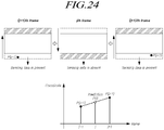
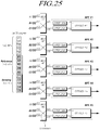
- the touch sensing circuit may operate by alternating group differential sensing directions for each frame.
- the touch sensing circuit may: select, as sensing touch electrodes, the k touch electrodes included in the second touch electrode group from among the g touch electrode groups; select, as reference touch electrodes, the k touch electrodes included in the first touch electrode group from among the g touch electrode groups; and match the k the touch electrodes included in the second touch electrode group and the k touch electrodes included in the first touch electrode group, so as to concurrently perform group differential sensing.
- Touch electrodes arranged in each touch electrode column may further include one additional touch electrode group including d touch electrodes, in addition to the g touch electrode groups, each of which includes k touch electrodes.
- d is a natural number equal to or larger than 1 and smaller than k.
- the touch sensing circuit may select, as sensing touch electrodes, the k touch electrodes including the d touch electrodes and the (k-d) touch electrodes arranged on the d touch electrodes, may select, as reference touch electrodes, the k touch electrodes arranged on the (k-d) touch electrodes, and may differentially sense the k touch electrodes selected as the sensing touch electrodes and the k touch electrodes selected as the reference touch electrodes.
- the touch display device may include a display panel in which multiple data lines and multiple gate lines are arranged.
- the multiple touch electrodes may be embedded in the display panel.
- the touch display device may perform display and touch sensing independently.
- the touch display device may concurrently perform display and touch sensing.
- a data signal for image display may be applied to the data lines.
- Each touch electrode column may be disposed so as to overlap with the data lines.
- a touch sensing circuit of embodiments of the present disclosure may include: k multiplexers that select, during a j-th frame for displaying an image, as sensing touch electrodes, the k touch electrodes (k ⁇ 2) included in a first touch electrode group among the g touch electrode groups (g ⁇ 2) in which multiple touch electrodes are grouped, and selects, as reference touch electrodes, the k touch electrodes included in a second touch electrode group other than the first touch electrode group from among the g touch electrode groups; and a differential sensing circuit that matches the k touch electrodes included in the first touch electrode group and the k touch electrodes included in the second touch electrode group so as to perform differential sensing.
- the k touch electrodes included in the first touch electrode group may be divided and connected to the k multiplexers, and the k multiplexers may select, as sensing touch electrodes, all the k touch electrodes included in the first touch electrode group so as to connect the selected k touch electrodes to positive input terminals of the k differential sensing circuits.
- the k touch electrodes included in the second touch electrode group may be divided and connected to the k multiplexers, and the k multiplexers may select, as reference touch electrodes, all the k touch electrodes included in the second touch electrode group so as to connect the selected k touch electrodes to negative input terminals of the k differential sensing circuits.
- the k multiplexers may select, as sensing touch electrodes, the k touch electrodes included in the second touch electrode group from among the g touch electrode groups, and may select, as reference touch electrodes, the k touch electrodes included in the first touch electrode group from among the g touch electrode groups; and the k differential sensing circuits may match the k touch electrodes included in the second touch electrode group and the k touch electrodes included in the first touch electrode group, so as to concurrently perform group differential sensing.
- Each of the k differential sensing circuits may be a sample-and-hold circuit or a differential amplifier.
- embodiments of the present disclosure relate to a method of driving a touch display device that includes multiple touch electrodes and a touch sensing circuit configured to sense the multiple touch electrodes, the method including: during a j-th frame for displaying an image, selecting, as sensing touch electrodes, k touch electrodes (k ⁇ 2) included in a first touch electrode group among g touch electrode groups (g ⁇ 2) in which multiple touch electrodes are grouped, and selecting, as reference touch electrodes, k touch electrodes included in a second touch electrode group other than the first touch electrode group from among the g touch electrode groups; and matching the k touch electrodes included in the first touch electrode group, i.e., a sensing touch electrode group, and the k touch electrodes included in the second touch electrode group, i.e., a reference touch electrode group, so as to perform differential sensing.
- the method may further include: during the j-th frame, after performing of the differential sensing, or during another frame other than the j-th frame, selecting, as sensing touch electrodes, the k touch electrodes included in the second touch electrode group from among the g touch electrode groups, and selecting, as reference touch electrodes, the k touch electrodes included in the first touch electrode group from among the g touch electrode groups; and matching the k touch electrodes included in the second touch electrode group, i.e., the sensing touch electrode group, and the k touch electrodes included in the first touch electrode group, i.e., the reference touch electrode group, so as to perform group differential sensing.
- the multiple touch electrodes may be embedded in the display panel in which multiple data lines and multiple gate lines are arranged.
- a data signal for image display may be applied to the data lines.
- Embodiments of the present disclosure described above may provide a touch display device, a touch sensing circuit, and a driving method, by which a touch sensing time can be significantly reduced.
- Embodiments of the present disclosure may provide the touch display device, the touch sensing circuit, and the driving method, by which excellent touch sensitivity and a fast touch sensing speed are allowed.
- Embodiments of the present disclosure may provide the touch display device, the touch sensing circuit, and the driving method, by which influence between display driving and touch driving can be reduced.
- Embodiments of the present disclosure may provide the touch display device, the touch sensing circuit, and the driving method, by which, even though display and touch sensing are concurrently performed, touch sensing is prevented from being influenced by display driving, so that touch sensitivity can be improved.
- Embodiments of the present disclosure may provide the touch display device, the touch sensing circuit, and the driving method, by which, when display and touch sensing are concurrently performed, undesired voltage fluctuation in touch electrodes due to voltage fluctuation of a display driving electrode, such as a data line, is prevented from occurring, so that touch sensitivity can be improved.
- first, second, A, B, (a), (b) or the like may be used herein when describing components of the present disclosure.
- Each of these terminologies is not used to define an essence, order, or sequence of a corresponding component but used merely to distinguish the corresponding component from other component (s) .
- another structural element may "be connected to", “be coupled to”, or “be in contact with” the structural elements as well as that the certain structural element is directly connected to or is in direct contact with another structural element.
- FIG. 1 is a schematic system configuration diagram of a touch display device according to embodiments of the present disclosure
- FIG. 2 is a diagram simply illustrating display driving of the touch display device according to embodiments of the present disclosure
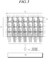
- FIG. 3 is a diagram simply illustrating touch driving of the touch display device according to embodiments of the present disclosure.
- a touch display device may provide a display function of displaying an image.
- the touch display device may provide a touch sensing function of sensing a user's touch, and a touch input function of performing input processing according to the user's touch by using a touch sensing result.
- display driving and elements for providing the display function are described with reference to FIG. 1 and FIG. 2
- touch driving and elements for providing the touch sensing function are described with reference to FIG. 1 and FIG. 3 .
- the touch display device may include: a display panel DISP in which, in order to provide a display function, multiple data lines DL and multiple gate lines GL may be arranged, and multiple subpixels SP defined by the multiple data lines DL and the multiple gate lines GL are arranged; a data driving circuit DDC that drives the multiple data lines DL; a gate driving circuit GDC that drives the multiple gate lines GL; and a display controller DCTR that controls the data driving circuit DDC and the gate driving circuit GDC.
- a display panel DISP in which, in order to provide a display function, multiple data lines DL and multiple gate lines GL may be arranged, and multiple subpixels SP defined by the multiple data lines DL and the multiple gate lines GL are arranged; a data driving circuit DDC that drives the multiple data lines DL; a gate driving circuit GDC that drives the multiple gate lines GL; and a display controller DCTR that controls the data driving circuit DDC and the gate driving circuit GDC.
- the display controller DCTR supplies various control signals to the data driving circuit DDC and the gate driving circuit GDC and controls the data driving circuit DDC and the gate driving circuit GDC.
- the display controller DCTR starts scanning according to timing implemented in each frame, converts input image data input from the outside according to a data signal format used in the data driving circuit DDC, outputs the converted image data, and controls data driving at an appropriate time for scanning.
- the gate driving circuit GDC sequentially supplies gate signals of an on-voltage and an off-voltage to the multiple gate lines GL according to control of the display controller DCTR.
- the data driving circuit DDC converts an image data signal received from the display controller DCTR into an image analog signal, and supplies a data signal Vdata corresponding thereto to the multiple data lines DL.
- the display controller DCTR may be a timing controller used in a typical display technology or a control device further performing other control functions, which includes the timing controller, and may be a control device differing from the timing controller.
- the display controller DCTR may be implemented as a part separate from the data driving circuit DDC and may be implemented as an integrated circuit together with the data driving circuit DDC.
- the data driving circuit DDC drives the multiple data lines DL by supplying the data signal Vdata to the multiple data lines DL.
- the data driving circuit DDC may be referred to as a "source driver”.
- This data driving circuit DDC may include at least one Source Driver Integrated Circuit (SDIC).
- SDIC Source Driver Integrated Circuit
- Each SDIC may include a shift register, a latch circuit, a Digital-to-Analog Converter (DAC), an output buffer circuit, and the like.
- DAC Digital-to-Analog Converter
- Each SDIC may further include an Analog-to-Digital Converter (ADC) according to circumstances.
- ADC Analog-to-Digital Converter
- Each SDIC may be connected to a bonding pad of the display panel DISP in a Tape Automated Bonding (TAB) scheme or a Chip On Glass (COG) scheme, or may be directly disposed in the display panel DISP, and may be integratedly disposed in the display panel DISP according to circumstances. Further, each SDIC may be implemented in a Chip On Film (COF) scheme, in which the SDIC is mounted on a film connected to the display panel DISP.
- TAB Tape Automated Bonding
- COG Chip On Glass
- the gate driving circuit GDC sequentially drives the multiple gate lines GL by sequentially supplying scan signals Vgate (also referred to as a scan voltage, a gate signal, or a gate voltage) to the multiple gate lines GSL.
- Vgate also referred to as a scan voltage, a gate signal, or a gate voltage
- the gate driving circuit GDC is referred to as a "scan driver”.
- the scan signal Vgate includes an off-level gate voltage causing a corresponding gate line GL to be closed and an on-level gate voltage causing the gate line GL to be open.
- the scan signal Vgate includes the off-level gate voltage causing a transistor connected to the gate line GL to be turned off and the on-level gate voltage causing the transistor connected to the gate line GL to be turned on.
- the off-level gate voltage may be a low-level gate voltage VGL
- the on-level gate voltage may be a high-level gate voltage VGH.
- the off-level gate voltage may be a high-level gate voltage VGH
- the on-level gate voltage may be a low-level gate voltage VGL.
- This gate driving circuit GDC may include at least one Gate Driver Integrated Circuit (GDIC).
- GDIC Gate Driver Integrated Circuit
- Each GDIC may include a shift register, a level shifter, and the like.
- Each GDIC may be connected to a bonding pad of the display panel DISP in a Tape Automated Bonding (TAB) scheme or a Chip On Glass (COG) scheme, or may be implemented in a Gate In Panel (GIP) type to be directly disposed in the display panel DISP, and may be integratedly disposed in the display panel (DISP) according to circumstances. Further, each GDIC may be implemented in a Chip On Film (COF) scheme, in which the GDIC is mounted on a film connected to the display panel DISP.
- TAB Tape Automated Bonding
- COG Chip On Glass
- GIP Gate In Panel
- COF Chip On Film
- the data driving circuit DDC may be positioned only on one side (e.g., the upper side or the lower side) of the display panel DISP, and may be positioned on both sides (e.g., an upper side and the lower side) of the display panel DISP according to a driving scheme, a panel design scheme, and the like according to circumstances.
- the gate driving circuit GDC may be positioned on only one side (e.g., the right side or the left side) of the display panel DISP, and may be positioned on both sides (e.g., the right side and the left side) of the display panel DISP according to a driving scheme, a panel design scheme, and the like according to circumstances.
- the touch display device may be various types of display devices, such as a liquid crystal display device, an organic light emitting display device, and the like.
- the display panel DISP according to the present embodiments may be various types of display panels, such as a liquid crystal display panel, an organic light emitting display panel, and the like.
- Each subpixel SP disposed in the display panel DISP may include one or more circuit elements (e.g., a transistor, a capacitor, etc.).
- a pixel electrode PXL may be disposed, and a transistor TR may be electrically connected between the pixel electrode PXL and the data lines DL.
- the transistor TR may be turned on by a scan signal Vgate supplied to a gate node through the gate lines GL, and when the transistor TR is turned on, a data signal Vdata supplied to a source node (or a drain node) through the data lines DL may be output to a drain node (or a source node), so that the data signal Vdata may be applied to the pixel electrode PXL electrically connected to the drain node (or the source node).
- An electric field is formed between the pixel electrode PXL, to which the data signal Vdata is applied, and a common electrode, to which a common voltage Vcom is applied, and a capacitance may be formed between the pixel electrode PXL and the common electrode.
- a structure of each subpixel SP may be variously determined according to a panel type, a provided function, a design scheme, and the like.
- the touch display device may include, in order to provide a touch sensing function, a touch panel TSP, a touch sensing circuit TDC that drives the touch panel TSP to perform sensing, a touch controller TCTR that performs sensing using a result of sensing the touch panel TSP, and the like.
- touch panel TSP In the touch panel TSP, a touch by a user's pointer may be made or brought close. In this touch panel TSP, touch sensors may be disposed.
- the user's pointer may be a finger, a pen, or the like.
- the pen may be a passive pen without a signal transmission/reception function or may be an active pen with a signal transmission/reception function.
- the touch sensing circuit TDC may supply a touch driving signal to the touch panel TSP, and may sense the touch panel TSP.
- the touch controller TCTR may sense a touch by using a result of sensing the touch panel TSP by the touch sensing circuit TDC.
- sensing the touch may refer to determining the presence or absence of the touch and/or determining touch coordinates.
- the touch panel TSP may be an external type disposed outside the display panel DISP or a built-in type disposed inside the display panel DISP.
- the touch panel TSP When the touch panel TSP is an external type, the touch panel TSP and the display panel DISP may be separately manufactured and then bonded together with an adhesive or the like.
- the external touch panel TSP may be referred to as an add-on type.
- the touch panel TSP When the touch panel TSP is a built-in type, the touch panel TSP may be manufactured together during a manufacturing process of the display panel DISP. That is, the touch sensors constituting the touch panel TSP may be disposed inside the display panel DISP.
- a built-in touch panel TSP may be an in-cell type, an on-cell type, a hybrid type, and the like.
- the touch panel TSP is a built-in type disposed inside the display panel DISP.
- the multiple touch electrodes TE may be included in the display panel DISP separately from electrodes used for display driving, and the electrodes that are disposed in the display panel DISP so as to perform display driving may be used as the multiple touch electrodes TE.
- common electrodes disposed in the display panel DISP may be divided into multiple common electrodes and used as the multiple touch electrodes TE. That is, the multiple touch electrodes TE disposed in the display panel DISP may be electrodes that perform touch sensing and may be electrodes perform displaying at the same time. In this case, a capacitance for display driving may be formed between the pixel electrode PXL and the touch electrodes TE functioning as the common electrodes.
- the multiple touch electrodes TE disposed in the display panel DISP are the common electrodes.
- the touch controller TCTR may be implemented as, for example, a micro control unit (MCU), a processor, and the like.
- MCU micro control unit
- the display controller DCTR and the touch controller TCTR may be implemented separately and may be implemented in an integrated manner.
- multiple touch electrodes TE may be disposed and multiple touch lines TL that electrically connect the multiple touch electrodes TE and the touch sensing circuit TDC may be disposed.
- one or more touch lines TL may be electrically connected through one or more contact holes.
- the touch lines TL electrically connected to the touch electrodes TE included in each touch electrode column may be disposed in parallel or overlapping with one or more data lines DL.
- the touch display device may sense a touch on the basis of self-capacitance of the touch electrodes TE or may sense a touch on the basis of mutual-capacitance between the touch electrodes TE.
- multiple first touch electrode lines and multiple second touch electrode lines are disposed to cross each other in the touch panel TSP.
- the multiple first touch electrode lines may be disposed in the X-axis direction
- the multiple second touch electrode lines may be disposed in the Y-axis direction.
- Each of the first touch electrode lines and the second touch electrode lines may be a single touch electrode in a bar shape and may be two or more electrically connected touch electrodes.
- the first touch electrode lines may be referred to as driving lines, driving electrodes, driving touch electrode lines, Tx lines, Tx electrodes, Tx touch electrode lines, or the like
- the second touch electrode lines may be referred to as reception lines, reception electrodes, reception touch electrode lines, sensing lines, sensing electrodes, sensing touch electrode lines, Rx lines, Rx electrodes, Rx touch electrode lines, or the like.
- the touch sensing circuit TDC may supply a driving signal to one or more among the multiple first touch electrode lines and senses the second touch electrode lines to output sensing data, and the touch controller TCTR may calculate the presence or absence of touch and/or touch coordinates by using the sensing data.
- the multiple touch electrodes TE may be disposed in a separated manner in the touch panel TSP.
- the touch sensing circuit TDC may supply a driving signal (hereinafter, referred to as a touch electrode driving signal (TDS)) to all or some of the multiple touch electrodes TE, and senses one or more touch electrodes TE, to which the driving signal has been supplied, to output sensing data, and the touch controller TCTR may calculate the presence or absence of touch and/or touch coordinates by using the sensing data.
- a driving signal hereinafter, referred to as a touch electrode driving signal (TDS)
- TDS touch electrode driving signal
- the touch display device senses a touch on the basis of self-capacitance
- the touch panel TSP is configured as illustrated in FIG. 2 and FIG. 3 .
- the touch electrode driving signal TDS output from the touch sensing circuit TDC may be a signal having a constant voltage and may be a signal having a variable voltage.
- the touch electrode driving signal TDS may have a variety of signal waveforms, for example, a sinusoidal waveform, a triangular waveform, or a square wave waveform.
- the touch electrode driving signal TDS is a signal having a variable voltage
- the touch electrode driving signal TDS is a pulse signal including multiple pulses.
- the touch electrode driving signal TDS may have a constant frequency or may have a variable frequency.
- the size of an area occupied by a single touch electrode TE may correspond to the size of an area occupied by a single subpixel SP, and may correspond to the size of an area occupied by two or more subpixels SP.
- the multiple touch electrodes TE are arranged in one touch electrode column, and multiple touch lines TL electrically connected to the multiple touch electrodes TE may overlap the multiple touch electrodes TE.
- the multiple touch electrodes TE arranged in one touch electrode column include a first touch electrode and a second touch electrode, a first touch line connected to the first touch electrode overlaps the second touch electrode, but may be electrically disconnected from the second touch electrode.
- the one touch electrode TE may overlap one or more data lines DL.
- each touch electrode column may overlap one or more data lines DL.
- each touch electrode row may overlap one or more gate lines GL.
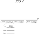
- FIG. 4 and FIG. 5 are diagrams for describing a Time Division Driving (TDD) scheme of the touch display device according to embodiments of the present disclosure.
- TDD Time Division Driving
- the touch display device may alternately perform display and touch sensing.
- the scheme, in which display driving for display and touch driving for touch sensing are alternately performed, is referred to as a time division driving scheme.
- a display period for display and a touch sensing period for touch sensing are alternated.
- the touch display device may perform display driving.
- the touch display device may perform touch driving.
- one frame time may be divided into one display period and one touch sensing period.
- one frame time may be divided into two or more display periods and one touch sensing period or two or more touch sensing periods.
- a touch electrode driving signal TDS may be applied to one or more among the multiple touch electrodes TE.
- the multiple data lines DL and the multiple gate lines GL may not be driven.
- unnecessary parasitic capacitance due to a potential difference may be generated between the touch electrode TE, to which the touch electrode driving signal TDS is applied, and one or more data lines DL positioned in the vicinity.
- the unnecessary parasitic capacitance may increase an RC delay for the touch electrode TE and a touch line TL connected thereto, so as to decrease touch sensitivity.
- the unnecessary parasitic capacitance due to a potential difference may also be generated between the touch electrode TE, to which the touch electrode driving signal TDS is applied, and one or more gate lines GL positioned in the vicinity.
- the unnecessary parasitic capacitance may increase an RC delay for the touch electrode TE and a touch line TL connected thereto, so as to decrease touch sensitivity.
- the unnecessary parasitic capacitance due to a potential difference may be generated between the touch electrode TE, to which the touch electrode driving signal TDS is applied, and one or more other touch electrodes TE positioned in the vicinity.
- the unnecessary parasitic capacitance may increase an RC delay for the touch electrode TE and a touch line TL connected thereto, so as to decrease touch sensitivity.
- the RC delay described above may be referred to as a time constant or a load.
- the touch display device may perform Load Free Driving (LFD) during the touch sensing period.
- LFD Load Free Driving
- the touch display device may apply, as a data signal Vdata, a load free driving signal to all data lines DL or some data lines DL which is likely to have parasitic capacitance formed therein.
- the touch display device may apply, as a gate signal Vgate, a load free driving signal to all gate lines GL or some gate lines GL which is likely to have parasitic capacitance formed therein.
- the touch display device may apply a load free driving signal to all other touch electrodes TE or some other touch electrodes TE which is likely to have parasitic capacitance formed therein.
- the described load free driving signal may be a touch electrode driving signal and may be a signal having the same or similar signal characteristic as that of the touch electrode driving signal.
- a frequency or a phase of the load free driving signal described above may be the same as a frequency and a phase of the touch electrode driving signal TDS, or may be the same as those of the touch electrode driving signal TDS with in a predetermined error range.
- the amplitude of the load free driving signal and the amplitude of the touch electrode driving signal TDS may be the same or may be the same within a predetermined error range, and there may be a deliberate difference in some cases.
- FIG. 6 is a diagram for describing a Time Free Driving (TFD) scheme of the touch display device according to embodiments of the present disclosure.
- TFD Time Free Driving
- the touch display device may perform display and touch sensing independently.
- the scheme, in which display driving for display and touch driving for touch sensing are independently performed, is referred to as a time free driving scheme.
- display driving for display and touch sensing driving for touch sensing may be concurrently performed. In some periods, only display driving for display may be performed or only touch driving for touch sensing may be proceeded.
- FIG. 7 is a diagram illustrating three cases (cases 1, 2, and 3) of time free driving when the touch display device according to embodiments of the present disclosure performs time free driving
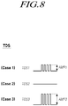
- FIG. 8 is a diagram illustrating a touch electrode driving signal (TDS) for each of three cases (cases 1, 2, and 3) of time free driving by the touch display device according to embodiments of the present disclosure.
- TDS touch electrode driving signal
- the touch display device may concurrently perform display driving and touch driving.
- the touch display device may supply a touch electrode driving signal TDS in the form of a variable voltage to the touch electrode TE in order to perform touch driving.
- the touch electrode driving signal TDS applied to the touch electrode TE is referred to as a first touch electrode driving signal TDS1.
- the first touch electrode driving signal TDS1 has a first amplitude AMP1.
- the touch display device may perform touch driving to sense a touch by a finger contact on the touch panel TSP.
- This touch sensing is referred to as finger sensing.
- the touch display device may perform touch driving to sense a touch by a finger or a pen in the case in which the finger or the pen is close to the touch panel TSP without touching the touch panel TSP.
- This touch sensing is referred to as hover sensing.
- the touch display device may perform only display driving.
- the touch display device does not perform normal touch driving because it is unnecessary to sense a touch by a finger. That is, the touch display device does not supply the touch electrode driving signal TDS in the form of a variable voltage to the multiple touch electrodes TE disposed in the touch panel TSP.
- the touch display device may supply the touch electrode driving signal TDS in the form of DC voltage.
- the touch electrode driving signal TDS applied to the touch electrode TE is referred to as a second touch electrode driving signal TDS2.
- the touch display device may receive a pen signal output from a pen through the touch electrode TE so as to sense the pen.
- the touch display device may obtain a pen sensing result, a position of the pen, a tilt, a pressure (writing pressure), or various additional information.
- the touch display device may perform only touch driving.
- the touch display device may supply a touch electrode driving signal TDS in the form of a variable voltage to the touch electrode TE in order to perform touch driving.
- the touch electrode driving signal TDS applied to the touch electrode TE is referred to as a third touch electrode driving signal TDS3.
- the third touch electrode driving signal TDS3 has a third amplitude AMP3 differing from the first amplitude AMP1.
- the touch display device may perform touch driving to sense a touch by a finger contact on the touch panel TSP.
- case 1 may be performed at a first active time
- case 3 may be performed at a blank time.
- the active time correspond to a time at which a screen of one frame is displayed
- the blank time may correspond to a time required to start displaying a screen of the next frame after the screen of one frame is displayed.
- case 1 may be switched to case 2.
- the touch display device may stop touch driving, for finger sensing to perform pen sensing while performing display driving and touch driving together (performing according to case 1) (that is, case 1 is switched to case 2).
- touch electrode driving signals TDS 1 and TDS 3 having amplitudes AMP1 and AMP3 may be applied to the touch electrode TE.
- the touch electrode driving signal TDS2 in the form of DC voltage may be applied to the touch electrode TE.
- the first amplitude AMP1 of the first touch electrode driving signal TDS1 applied to the touch electrode TE when display driving is performed together with touch driving (case 1) may be smaller than the third amplitude AMP3 of the third touch electrode driving signal TDS3 applied to the touch electrode TE when only touch driving is performed (case 3).
- the first amplitude AMP1 of the first touch electrode driving signal TDS1 applied to the touch electrode TE during the active time may be smaller than the third amplitude AMP3 of the third touch electrode driving signal TDS3 applied to the touch electrode TE during the blank time.
- the touch sensing circuit TDC may supply, to the multiple touch electrodes TE, the first touch electrode driving signal TDS1 having the first amplitude AMP1 and the second touch electrode driving signal TDS2 corresponding to the DC voltage.
- the touch sensing circuit TDC may supply the third touch electrode driving signal TDS3 having the third amplitude AMP3 to one or more among the multiple touch electrodes TE.
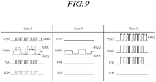
- FIG. 9 is a diagram summarizing and illustrating waveforms of main signals (TDS1, Vdata, VGL_M, and VGH_M) for each of three cases (case 1, case 2, and case 3) of time free driving in the touch display device according to embodiments of the present disclosure.
- Case 1 and case 2 are driving cases during an active time.
- Case 3 is a driving case during a blank time.
- a touch electrode driving signal TDS applied to the touch electrode TE, a data signal Vdata applied to the data line DL, an on-level gate voltage VGH and an off-level gate voltage VGL supplied to a gate driving circuit GDC to generate a scan signal Vgate supplied to the gate line GL will be examined.
- the touch electrode driving signal TDS applied to the touch electrode TE is a second touch electrode driving signal TDS2 in the form of DC voltage.
- the data signal Vdata applied to the data line DL may be a signal corresponding to an image analog signal, in which an image digital signal is digital-to-analog converted for display, and may be a pixel voltage applied to a pixel electrode PXL of a corresponding subpixel SP through the data line DL.
- the data signal Vdata may be a voltage fluctuation between a driving voltage AVDD and a ground voltage AVSS.
- Each of the off-level gate voltage VGL and the on-level gate voltage VGH included in the scan signal Vgate applied to the gate line GL is corresponding DC voltage.
- the touch electrode TE may function as a common electrode that performs display driving. Therefore, in the case 2 in which only display driving is performed during the active time, the second touch electrode driving signal TDS2 applied to the touch electrode TE corresponds to a common voltage for display.
- the touch electrode driving signal TDS3 applied to the touch electrode TE is a third touch electrode driving signal TDS3 having the third amplitude AMP3.
- the data line DL may be applied with the data signal Vdata corresponding to the DC voltage, or may be in a floating state.
- the scan signal Vgate configured by the off-level gate voltage VGL corresponding to the DC voltage may be applied to the gate line GL.
- the data line DL and the gate line GL may be oscillated in the same manner as the touch electrode TE in terms of voltage characteristics.
- the data signal Vdata applied to the data line DL may be the third touch electrode driving signal TDS3or may be a load free driving signal, the signal characteristic (e.g., a phase, a frequency, an amplitude, etc.) of which is similar to or the same as that of the third touch electrode driving signal TDS3.
- the signal characteristic e.g., a phase, a frequency, an amplitude, etc.
- the off-level gate voltage VGL applied to the gate line GL may be the third touch electrode driving signal TDS3or may be a load free driving signal, the signal characteristic (e.g., a phase, a frequency, an amplitude, etc.) of which is similar to or the same as that of the third touch electrode driving signal TDS3.
- the signal characteristic e.g., a phase, a frequency, an amplitude, etc.
- the touch electrode driving signal TDS applied to the touch electrode TE is a first touch electrode driving signal TDS1 having a first amplitude AMP1.
- the first touch electrode driving signal TDS1 may be a driving signal for touch sensing, and may be a common voltage Vcom for display at the same time.
- the first touch electrode driving signal TDS1 applied to the touch electrode TE may be required to have a determined voltage difference for display with the data signal Vdata corresponding to the pixel voltage for display.
- the first touch electrode driving signal TDS1 performs two functions (a driving signal for touch sensing and a common voltage for display).
- the common voltage Vcom corresponding to the first touch electrode driving signal TDS1 is not a constant voltage and is a variable voltage, in order to prevent the data line DL from being influenced by touch driving, there should be, for the data signal Vdata, additional voltage fluctuation as much as the first amplitude AMP1 of the first touch electrode driving signal TDS 1 in addition to original voltage fluctuation for display.
- a voltage fluctuation part i.e., the first amplitude AMP1
- the first touch electrode driving signal TDS1 is excluded, and only the original voltage fluctuation for display is present. Accordingly, normal display may be possible.
- the data signal Vdata of case 1, in which display driving and touch driving are concurrently performed may be a signal of the form in which the data signal Vdata of a case (case 2), in which only display driving is performed, and the first touch electrode driving signal TDS1 are combined.
- the data signal Vdata of case 1 in which display driving and touch driving are concurrently performed, may be a signal of the form in which the original data signal Vdata of the case (case 2), in which only display driving is performed, is offset by the first touch electrode driving signal TDS1.
- the data signal Vdata may be a voltage fluctuation between a driving voltage AVDD and a ground voltage AVSS.
- the voltage difference between the data signal Vdata in case 1, in which touch driving and display driving are concurrently performed, and the first touch electrode driving signal TDS1 is the same as the voltage difference between the data signal Vdata in case 2, in which only display driving is performed, and the second touch electrode driving signal TDS2.
- load free driving may be required.
- each of the on-level gate voltage VGH and the off-level gate voltage VGL supplied to the gate driving circuit GDC may be a load free driving signal, the signal characteristic (e.g., a phase, a frequency, an amplitude, etc.) of which is similar to or the same as that of the third touch electrode driving signal TDS3.
- the signal characteristic e.g., a phase, a frequency, an amplitude, etc.
- FIG. 10 is a diagram simply illustrating an analog front-end AFE within a touch sensing circuit TDC of the touch display device according to embodiments of the present disclosure.
- the touch sensing circuit TDC includes an analog front-end AFE including a preamplifier PAMP, an integrator INTG, and the like.
- the preamplifier PAMP has a first input terminal IN1, a second input terminal IN2, and an output terminal.
- a touch electrode driving signal TDS (TDS1 or TDS3 of FIG. 9 ) in a pulse signal form is input to the first input terminal IN1.
- the second input terminal IN2 may be electrically connected to a touch line TL that is connected to a touch electrode TE to be sensed in the display panel DISP.
- the touch electrode driving signal TDS input to the first input terminal IN1 may be applied to the touch electrode TE through the second input terminal IN2.
- a feedback capacitor Cfb may be electrically connected between the second input terminal IN2 and the output terminal OUT.
- the feedback capacitor Cfb may be charged.
- the charging amount of the feedback capacitor Cfb may vary depending on whether a touch pointer (e.g., a finger, a pen, etc.) touches or is close to the touch electrode TE.
- FIG. 11 is a diagram illustrating a single-ended sensing scheme of the touch display device according to embodiments of the present disclosure.
- one analog front-end AFE may sense a touch electrode TE to be touch-sensed, as shown in FIG. 10 .
- This sensing scheme is referred to as a "single-ended sensing scheme".
- the single-ended sensing scheme will be described as an example.
- M ⁇ N touch electrodes TE disposed in the display panel DISP may be arranged in M rows and N columns.
- M may be a natural number of 2 or greater, and N may be a natural number of 2 or greater.
- the touch display device may include N analog front-ends AFE#1-AFE#N.
- the N analog front-ends AFE#1-AFE#N may correspond one-to-one to the N touch electrodes TE arranged in the first row, and may sense the N touch electrodes TE.
- the DTX phenomenon may further become worse when each touch electrode TE column is overlappingly disposed with one or more data lines DL.
- unnecessary noise may occur in a touch electrode column parallel to the data line DL due to voltage fluctuation of the data line DL.
- the occurrence of the unnecessary noise may correspond to occurrence of the DTX phenomenon, may degrade a touch sensing performance, and may degrade a display performance in some cases.
- the touch display device may "differentially sense" two touch electrodes TE arranged in a direction in which the data line DL is disposed.
- FIG. 12 and FIG. 13 are diagrams simply illustrating an analog front-end AFE within a touch sensing circuit TDC when the touch display device performs differential sensing according to embodiments of the present disclosure.
- the analog front-end AFE within the touch sensing circuit TDC may include a differential sensing circuit DIFFSEN.
- the differential sensing circuit DIFFSEN may output or store a difference between voltages input to a positive input terminal pi and a negative input terminal ni, respectively.
- the positive input terminal pi of the differential sensing circuit DIFFSEN is connected to an output terminal OUT of a first preamplifier PAMP_SEN that detects a signal of a touch electrode TE1 to be sensed.
- the negative input terminal ni of the differential sensing circuit DIFFSEN is connected to an output terminal OUT of a second preamplifier PAMP_REF that detects a signal of another touch electrode TE2 other than the touch electrode TE1 to be sensed.
- the touch electrode TE2 other than the touch electrode TE1 to be sensed is also referred to as a touch electrode TE serving as a reference for differential sensing.
- two touch electrodes TE1 and TE2 to be differentially sensed may include the touch electrode TE1 to be sensed and the touch electrode TE serving as a reference, and may be touch electrodes disposed in parallel with a direction in which the data lines DL are extended (column direction).
- the two touch electrodes TE1 and TE2 to be differentially sensed may be touch electrodes arranged in the same touch electrode column.
- the differential sensing circuit DIFFSEN may be a Sample-and-Hold Circuit SHA.
- the differential sensing circuit DIFFSEN may be a differential amplifier DAMP.
- the first preamplifier PAMP_SEN may be electrically connected between the positive input terminal pi of the differential sensing circuit DIFFSEN and the touch electrode TE1 to be sensed.
- the second preamplifier PAMP_REF may be electrically connected between the negative input terminal ni of the differential sensing circuit and the touch electrode TE2 serving as a reference.
- a first integrator INTG_SEN may be electrically connected between the positive input terminal pi of the differential sensing circuit DIFFSEN and the first preamplifier PAMP_SEN.
- a second integrator INTG_REF may be electrically connected between the negative input terminal ni of the differential sensing circuit DIFFSEN and the second preamplifier PAMP_REF.
- the differential sensing circuit DIFFSEN stores or outputs a difference between an integration value output from the first integrator INTG_SEN and an integration value output from the second integrator INTG_REF so as to perform differential sensing, more accurate differential sensing may be possible.
- a value output from the differential sensing circuit DIFFSEN may be input to the analog-to-digital converter ADC.
- an integrator INTG may be connected to the output terminal of the differential sensing circuit DIFFSEN. In this case, it is beneficial to reduce the number of integrators INTG.
- the value output from the integrator INTG may be input to the analog-to-digital converter ADC.
- FIG. 14 to FIG. 16 are diagrams illustrating a sequential differential sensing scheme of the touch display device according to embodiments of the present disclosure.
- the touch display device may differentially sense two touch electrodes TE included in the same column according to a differential sensing scheme.
- M ⁇ N touch electrodes disposed in the display panel DISP may be arranged in M rows and N columns.
- M may be a natural number of 2 or greater, and N may be a natural number of 2 or greater.
- the touch display device may include N analog front-ends AFE#1-AFE#N.
- the N touch electrodes TE arranged in the first row are touch electrodes to be sensed and the N touch electrodes TE arranged in a second row are touch electrodes serving as a reference
- the N analog front-ends AFE#1-AFE#N may differentially sense the N touch electrodes TE arranged in the first row and the N touch electrodes TE arranged in the second row.
- a "+" sign represents the positive input terminal pi of the differential sensing circuit DIFFSEN in FIG. 12 and FIG. 13 .
- a "-" sign represents the negative input terminal ni of the differential sensing circuit DIFFSEN in FIG. 12 and FIG. 13 .
- a scheme of differentially sensing two touch electrodes TE which are directly adjacent and included in the same touch electrode column, is referred to as a "sequentially differential sensing scheme".
- the ten touch electrodes TE1-TE10 represent ten touch electrode rows (TE row) .
- the touch sensing circuit TDC differentially senses (1st differential sensing) TE1 (a touch electrode to be sensed) and TE2 (a reference touch electrode), continues differential sensing (2nd differential sensing) of TE2 (a touch electrode to be sensed) and TE3 (a reference touch electrode), continues differential sensing (3rd differential sensing) of TE3 (a touch electrode to be sensed) and TE4 (a reference touch electrode), continues differential sensing (4th differential sensing) of TE4 (a touch electrode to be sensed) and TE5 (a reference touch electrode), and then continues differential sensing (5rh differential sensing) of TE5 (a touch electrode to be sensed) and TE6 (a reference touch electrode).
- touch coordinates are obtained after, for example, first to fifth differential sensing is sequentially performed, that is, for pulse signals PWM for first to fifth differential sensing, after the touch electrode driving signal TDS is supplied to the display panel DISP, five driving times are required for the first to fifth differential sensing.
- the touch display device proposes a "group differential sensing scheme" that is a new differential sensing scheme, by which a sensing time may be reduced, finger/pen local sensing may be possible, and deterioration of touch sensitivity may also be prevented.
- a “group differential sensing scheme” will be described in detail.
- FIG. 17 and FIG. 18 are diagrams illustrating a group differential sensing scheme of the touch display device according to embodiments of the present disclosure.
- ten touch electrodes TE1-TE10 included in a first touch electrode column (1st TE column) are grouped into a single group (hereinafter, referred to as a "touch electrode group (TEG)").
- the ten touch electrodes TE1-TE10 represent ten touch electrode rows (TE row).
- FIG. 17 shows a case in which, among ten touch electrodes TE1-TE10, first five touch electrodes TE1-TE5 are grouped into one group of a first touch electrode group TEG#A, and following five touch electrodes TE6-TE10 are grouped into another group of a second touch electrode group TEG#B.
- the touch sensing circuit TDC when performing a first group differential sensing, selects, as sensing touch electrodes, five touch electrodes TE1-TE5 included in the first touch electrode group TEG#A and concurrently senses the selected five touch electrodes TE1-TE5. Thereafter, when performing a second group differential sensing, the touch sensing circuit TDC selects, as sensing touch electrodes, five touch electrodes TE6-TE10 included in the second touch electrode group TEG#B, and concurrently senses the selected five touch electrodes TE6-TE10.
- the touch sensing circuit TDC may select, as sensing touch electrodes, five touch electrodes TE1-TE5 included in the first touch electrode group TEG#A, may select, as reference touch electrodes, five touch electrodes TE6-TE10 included in the second touch electrode group TEG#B, and may match the five touch electrodes TE1-TE5 included in the first touch electrode group TEG#A and the five touch electrodes TE6-TE10 included in the second touch electrode group TEG#B, so as to perform differential sensing.
- the touch sensing circuit TDC may concurrently perform differential sensing for TE1 (sensing touch electrode) and TE6 (reference touch electrode), differential sensing for TE2 (sensing touch electrode) and TE7 (reference touch electrode), differential sensing for TE3 (sensing touch electrode) and TE8 (reference touch electrode), differential sensing for TE4 (sensing touch electrode) and TE9 (reference touch electrode), and differential sensing for TE5 (sensing touch electrode) and TE10 (reference touch electrode).
- a second group differential sensing between the second touch electrode group TEG#B and another touch electrode group following thereafter may be performed.
- Sensing data obtained as a result of the first group differential sensing is sensing data of the five touch electrodes TE1-TE5 included in the first touch electrode group TEG#A. Further, sensing data obtained as a result of the second group differential sensing is sensing data of the five touch electrodes TE6-TE10 included in the second touch electrode group TEG#B.
- time required to obtain touch coordinates by sensing five touch electrodes TE1-TE5 included in the first touch electrode group TEG#A has been reduced to 1/5 of time required to obtain touch coordinates by sensing the same five touch electrodes TE1-TE5 according to the sequential differential sensing scheme in FIG. 16 .
- a sensing time may be reduced, finger/pen local sensing may be possible, and deterioration of touch sensitivity may also be prevented.
- the touch sensing circuit TDC may receive a pen signal output from a pen via at least one of multiple touch electrodes TE.
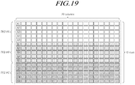
- FIG. 19 is an exemplary diagram of touch electrode TE arrangement for describing an exemplary group differential sensing scheme of the touch display device according to embodiments of the present disclosure
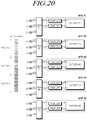
- FIG. 20 is a diagram simply illustrating, in order to describe the exemplary group differential sensing scheme of the touch display device, structures of analog front-ends AFE and multiplexers for group differential sensing with respect to each touch electrode column (TE column) in the touch electrode arrangement structure in FIG. 19 according to embodiments of the present disclosure.
- FIG. 21 and FIG. 22 are diagrams illustrating a group differential sensing procedure with respect to each touch electrode column (TE column) during a j-th frame according to embodiments of the present disclosure.
- the touch display device may include multiple touch electrodes TE, a touch sensing circuit TDC that senses the multiple touch electrodes TE for each group, and the like.
- g represents the number of the touch electrode groups, i.e., aggregates of concurrently sensible touch electrodes, and may be a natural number of 2 or greater.
- K represents the number of touch electrode rows included in one touch electrode group and may be a natural number of 2 or greater.
- k represents the number of touch electrodes included in one touch electrode group and may be a natural number of 2 or greater.
- M which represents the number of touch electrode rows is (g ⁇ k).
- M touch electrodes TE disposed in each touch electrode column TE may be grouped into g touch electrode groups TEG#A, TEG#B, and TEG#C, each of which includes k touch electrodes TE, and an additional touch electrode group TEG #D including d touch electrodes, in which d is different from k.
- first touch electrode column five touch electrodes may be included in each of three touch electrode groups TEG#A, TEG#B, and TEG#C. More particularly, five touch electrodes A1-A5 are included in the first touch electrode group TEG#A.
- Five touch electrodes B1-B5 are included in the second touch electrode group TEG#B.
- Five touch electrodes C1-C5 are included in the third touch electrode group TEG#C.
- the touch sensing circuit TDC may select, as sensing touch electrodes, five touch electrodes A1-A5 included in the first touch electrode group TEG#A from among three touch electrode groups TEG#A, TEG#B, and TEG#C, may select, as reference touch electrodes, five touch electrodes B1-B5 included in the second touch electrode group TEG#B from among three touch electrode groups TEG#A, TEG#B, and TEG#C, and then may match the five touch electrodes A1-A5 included in the first touch electrode group TEG#A and the five touch electrodes B1-B5 included in the second touch electrode group TEG#B, so as to perform differential sensing.
- the touch sensing circuit TDC may concurrently perform differential sensing for the touch electrode A1 (sensing touch electrode) and the touch electrode B1 (reference touch electrode), differential sensing for the touch electrode A2 (sensing touch electrode) and the touch electrode B2 (reference touch electrode), differential sensing for the touch electrode A3 (sensing touch electrode) and the touch electrode B3 (reference touch electrode), differential sensing for the touch electrode A4 (sensing touch electrode) and the touch electrode B4 (reference touch electrode), and differential sensing for the touch electrode A5 (sensing touch electrode) and the touch electrode B5 (reference touch electrode).
- the number of the multiplexers and the number of the differential sensing circuits may be the same as k which represents the number of touch electrode rows within a single touch electrode group (the number of touch electrodes within the touch electrode group in a single touch electrodecolumn).
- Each of the k multiplexers MUX#1-MUX#5 may select one sensing channel and one reference channel from among g channels ch1-ch3.
- Each of the k differential sensing circuits DIFFSEN#1-DIFFSEN#5 may have a positive input terminal pi and a negative input terminal ni.
- the positive input terminal pi and the negative input terminal ni of each of the k differential sensing circuits DIFFSEN#1-DIFFSEN#5 may be electrically connected to a sensing channel connection terminal sch and a reference channel connection terminal rch of each of the k multiplexers MUX#1-MUX#5.
- the k differential sensing circuits DIFFSEN#1-DIFFSEN#5 may match the five touch electrodes A1-A5 included in the first touch electrode group TEG#A that is a sensing touch electrode group and the five touch electrodes B1-B5 included in the second touch electrode group TEG#B that is a reference touch electrode group, so as to perform differential sensing.
- each of the five differential sensing circuits DIFFSEN#1-DIFFSEN#5 may include a positive input terminal pi, a negative input terminal ni, and an output terminal.
- the positive input terminal pi may be electrically connected to one of the five touch electrodes A1-A5 included in the first touch electrode group TEG#A, which have been selected as sensing touch electrodes.
- the negative input terminal ni may be electrically connected to one of the five touch electrodes B1-B5 included in the second touch electrode group TEG#B, which have been selected as reference touch electrodes.
- the output terminal may be stored or output a voltage difference between the positive input terminal pi and the negative input terminal ni.
- the first touch electrode group TEG#A among three touch electrode groups TEG#A, TEG#B, and TEG#C may be positioned closer to the touch sensing circuit TDC compared to the second touch electrode group TEG#B.
- the second touch electrode group TEG#B among three touch electrode groups TEG#A, TEG#B, and TEG#C may be positioned closer to the touch sensing circuit TDC compared to the first touch electrode group TEG#A.
- each of the k differential sensing circuits DIFFSEN#1-DIFFSEN#5 may be a sample-and-hold circuit SHA or a differential amplifier DAMP.
- a circuit structure will be examined in terms of an i-th multiplexer (i is one of numbers from 1 to k) among the k multiplexers MUX#1-MUX#5 and an i-th differential sensing circuit corresponding to the i-th multiplexer from among the k differential sensing circuits DIFFSEN#1-DIFFSEN#5.
- a first preamplifier PAMP_SEN electrically connected between a sensing channel connection terminal sch of the i-th multiplexer and a positive input terminal pi of the i-th differential sensing circuit, and a second preamplifier PAMP_REF electrically connected between a reference channel connection terminal rch of the i-th multiplexer and a negative input terminal ni of the i-th differential sensing circuit may be included.
- FIG. 20 is a circuit structure in which an integrator configuration is omitted.
- a first integrator INTG_SEN may be connected between the positive input terminal pi of the i-th differential sensing circuit and the first preamplifier PAMP_SEN
- a second integrator INTG_REF may be connected between the negative input terminal ni of the i-th differential sensing circuit and the second preamplifier PAMP_REF.
- one integrator INTG may be connected to an output terminal of the i-th differential sensing circuit.
- Each of the k multiplexers MUX#1-MUX#5 may select one sensing channel and one reference channel from among g channels ch1-ch3.
- Each of the k differential sensing circuits DIFFSEN#1-DIFFSEN#5 may have a positive input terminal pi and a negative input terminal ni.
- the i-th multiplexer among the k multiplexers MUX#1-MUX#5 may be connected to the i-th differential sensing circuit among the k differential sensing circuits DIFFSEN#1-DIFFSEN#5.
- i may be one of numbers from 1 to k.
- the i-th multiplexer may select one sensing channel and one reference channel from among the g channels ch1-ch3, and may connect the selected sensing channel and reference channel to a sensing channel connection terminal sch and a reference channel connection terminal rch, respectively.
- the g channels ch1-ch3 of the i-th multiplexer may correspond to i-th touch electrodes in each of the g touch electrode groups TEG#A, TEG#B, and TEG#C, respectively.
- the sensing channel connection terminal sch of the -th multiplexer may be electrically connected to the positive input terminal pi of the i-th differential sensing circuit.
- the reference channel connection terminal sch of the i-th multiplexer may be connected to the negative input terminal ni of the i-th differential sensing circuit.
- FIG. 21 is a diagram illustrating a procedure of, when the first touch electrode group TEG#A is a sensing touch electrode group and the second touch electrode group TEG#B is a reference touch electrode group, performing group differential sensing of the first touch electrode group TEG#A and the second touch electrode group TEG#B, so as to obtain sensing data for the first touch electrode group TEG#A.
- the five touch electrodes A1-A5 included in the first touch electrode group TEG#A are sensing touch electrodes, and may correspond to sensing channels selected from five multiplexers MUX#1-MUX#5, respectively.
- the five touch electrodes B1-B5 included in the second touch electrode group TEG#B are reference touch electrodes, and may correspond to reference channels selected from five multiplexers MUX#1-MUX#5, respectively.
- the first multiplexer MUX#1 may select one sensing channel ch1 and one reference channel ch2 from among three channels ch1-ch3, and may connect the selected sensing channel ch1 and reference channel ch2 to the sensing channel connection terminal sch and the reference channel connection terminal rch, respectively.
- three channels ch1-ch3 of the first multiplexer MUX#1 may correspond to first touch electrodes A1, B1, and C1 in three touch electrode groups TEG#A, TEG#B, and TEG#C, respectively.
- the sensing channel connection terminal sch of the first multiplexer MUX#1 may be electrically connected to the positive input terminal pi of the first differential sensing circuit DIFFSEN#1.
- the reference channel connection terminal rch of the first multiplexer MUX#1 may be connected to the negative input terminal ni of the first differential sensing circuit DIFFSEN#1.
- the first differential sensing circuit DIFFSEN#1 may differentially sense a first touch electrode A1 in the first touch electrode group TEG#A corresponding to the sensing channel ch1 and a first touch electrode B1 in the second touch electrode group TEG#B corresponding to the reference channel ch2.
- the second multiplexer MUX#2 may select one sensing channel ch1 and one reference channel ch2 from among three channels ch1-ch3, and may connect the selected sensing channel ch1 and reference channel ch2 to the sensing channel connection terminal sch and the reference channel connection terminal rch, respectively.
- three channels ch1-ch3 of the second multiplexer MUX#2 may correspond to second touch electrodes A2, B2, and C2 in three touch electrode groups TEG#A, TEG#B, and TEG#C, respectively.
- the sensing channel connection terminal sch of the second multiplexer MUX#2 may be electrically connected to the positive input terminal pi of the second differential sensing circuit DIFFSEN#2.
- the reference channel connection terminal rch of the second multiplexer MUX#2 may be connected to the negative input terminal ni of the second differential sensing circuit DIFFSEN#2.
- the second differential sensing circuit DIFFSEN#2 may differentially sense a second touch electrode A2 in the first touch electrode group TEG#A corresponding to the sensing channel ch1 and a second touch electrode B2 in the second touch electrode group TEG#B corresponding to the reference channel ch2.
- the third multiplexer MUX#3 may select one sensing channel ch1 and one reference channel ch2 from among three channels ch1-ch3, and may connect the selected sensing channel ch1 and reference channel ch2 to the sensing channel connection terminal sch and the reference channel connection terminal rch, respectively.
- three channels ch1-ch3 of the third multiplexer MUX#3 may correspond to third touch electrodes A3, B3, and C3 in three touch electrode groups TEG#A, TEG#B, and TEG#C, respectively.
- the sensing channel connection terminal sch of the third multiplexer MUX#3 may be electrically connected to the positive input terminal pi of the third differential sensing circuit DIFFSEN#3.
- the reference channel connection terminal rch of the third multiplexer MUX#3 may be connected to the negative input terminal ni of the third differential sensing circuit DIFFSEN#3.
- the third differential sensing circuit DIFFSEN#3 may differentially sense a third touch electrode A3 in the first touch electrode group TEG#A corresponding to the sensing channel ch1 and a third touch electrode B3 in the second touch electrode group TEG#B corresponding to the reference channel ch2.
- the fourth multiplexer MUX#4 may select one sensing channel ch1 and one reference channel ch2 from among three channels ch1-ch3, and may connect the selected sensing channel ch1 and reference channel ch2 to the sensing channel connection terminal sch and the reference channel connection terminal rch, respectively.
- three channels ch1-ch3 of the fourth multiplexer MUX#4 may correspond to fourth touch electrodes A4, B4, and C4 in three touch electrode groups TEG#A, TEG#B, and TEG#C, respectively.
- the sensing channel connection terminal sch of the fourth multiplexer MUX#4 may be electrically connected to the positive input terminal pi of the fourth differential sensing circuit DIFFSEN#4.
- the reference channel connection terminal rch of the fourth multiplexer MUX#4 may be connected to the negative input terminal ni of the fourth differential sensing circuit DIFFSEN#4.
- the fourth differential sensing circuit DIFFSEN#4 may differentially sense a fourth touch electrode A4 in the first touch electrode group TEG#A corresponding to the sensing channel ch1 and a fourth touch electrode B4 in the second touch electrode group TEG#B corresponding to the reference channel ch2.
- the fifth multiplexer MUX#5 may select one sensing channel ch1 and one reference channel ch2 from among three channels ch1-ch3, and may connect the selected sensing channel ch1 and reference channel ch2 to the sensing channel connection terminal sch and the reference channel connection terminal rch, respectively.
- three channels ch1-ch3 of the fifth multiplexer MUX#5 may correspond to fifth touch electrodes A5, B5, and C5 in three touch electrode groups TEG#A, TEG#B, and TEG#C, respectively.
- the sensing channel connection terminal sch of the fifth multiplexer MUX#5 may be electrically connected to the positive input terminal pi of the fifth differential sensing circuit DIFFSEN#5.
- the reference channel connection terminal rch of the fifth multiplexer MUX#5 may be connected to the negative input terminal ni of the fifth differential sensing circuit DIFFSEN#5.
- the fifth differential sensing circuit DIFFSEN#5 may differentially sense a fifth touch electrode A5 in the first touch electrode group TEG#A corresponding to the sensing channel ch1 and a fifth touch electrode B5 in the second touch electrode group TEG#B corresponding to the reference channel ch2.
- Connection operations of the respective five multiplexers MUX#1-MUX#5 are concurrently performed, and differential sensing operations of the respective five differential sensing circuits DIFFSEN#1-DIFFSEN#5 are concurrently performed.
- sensing data for the first touch electrode group TEG#A may be obtained in a short time by performing group differential sensing of the first touch electrode group TEG#A and the second touch electrode group TEG#B.
- FIG. 22 is a diagram illustrating a procedure of obtaining, when the second touch electrode group TEG#B is a sensing touch electrode group and the third touch electrode group TEG#C is a reference touch electrode group, sensing data for the second touch electrode group TEG#B by performing group differential sensing of the second touch electrode group TEG#B and the third touch electrode group TEG#C.
- the five touch electrodes B1-B5 included in the second touch electrode group TEG#B are sensing touch electrodes, and may correspond to sensing channels selected from five multiplexers MUX#1-MUX#5, respectively.
- the five touch electrodes C1-C5 included in the third touch electrode group TEG#C are reference touch electrodes, and may correspond to reference channels selected from five multiplexers MUX#1-MUX#5, respectively.
- the first multiplexer MUX#1 may select one sensing channel ch2 and one reference channel ch3 from among three channels ch1-ch3, and may connect the selected sensing channel ch2 and reference channel ch3 to the sensing channel connection terminal sch and the reference channel connection terminal rch, respectively.
- the sensing channel connection terminal sch of the first multiplexer MUX#1 may be electrically connected to the positive input terminal pi of the first differential sensing circuit DIFFSEN#1.
- the reference channel connection terminal rch of the first multiplexer MUX#1 may be connected to the negative input terminal ni of the first differential sensing circuit DIFFSEN#1.
- the first differential sensing circuit DIFFSEN#1 may differentially sense a first touch electrode B1 in the second touch electrode group TEG#B corresponding to the sensing channel ch2 and a first touch electrode C1 in the third touch electrode group TEG#C corresponding to the reference channel ch3.
- the second multiplexer MUX#2 may select one sensing channel ch2 and one reference channel ch3 from among three channels ch1-ch3, and may connect the selected sensing channel ch2 and reference channel ch3 to the sensing channel connection terminal sch and the reference channel connection terminal rch, respectively.
- the sensing channel connection terminal sch of the second multiplexer MUX#2 may be electrically connected to the positive input terminal pi of the second differential sensing circuit DIFFSEN#2.
- the reference channel connection terminal rch of the second multiplexer MUX#2 may be connected to the negative input terminal ni of the second differential sensing circuit DIFFSEN#2.
- the second differential sensing circuit DIFFSEN#2 may differentially sense a second touch electrode B2 in the second touch electrode group TEG#B corresponding to the sensing channel ch2 and a second touch electrode C2 in the third touch electrode group TEG#C corresponding to the reference channel ch3.
- the third multiplexer MUX#3 may select one sensing channel ch2 and one reference channel ch3 from among three channels ch1-ch3, and may connect the selected sensing channel ch2 and reference channel ch3 to the sensing channel connection terminal sch and the reference channel connection terminal rch, respectively.
- the sensing channel connection terminal sch of the third multiplexer MUX#3 may be electrically connected to the positive input terminal pi of the third differential sensing circuit DIFFSEN#3.
- the reference channel connection terminal rch of the third multiplexer MUX#3 may be connected to the negative input terminal ni of the third differential sensing circuit DIFFSEN#3.
- the third differential sensing circuit DIFFSEN#3 may differentially sense a third touch electrode B3 in the second touch electrode group TEG#B corresponding to the sensing channel ch2 and a third touch electrode C3 in the third touch electrode group TEG#C corresponding to the reference channel ch3.
- the fourth multiplexer MUX#4 may select one sensing channel ch2 and one reference channel ch3 from among three channels ch1-ch3, and may connect the selected sensing channel ch2 and reference channel ch3 to the sensing channel connection terminal sch and the reference channel connection terminal rch, respectively.
- the sensing channel connection terminal sch of the fourth multiplexer MUX#4 may be electrically connected to the positive input terminal pi of the fourth differential sensing circuit DIFFSEN#4.
- the reference channel connection terminal rch of the fourth multiplexer MUX#4 may be connected to the negative input terminal ni of the fourth differential sensing circuit DIFFSEN#4.
- the fourth differential sensing circuit DIFFSEN#4 may differentially sense a fourth touch electrode B4 in the second touch electrode group TEG#B corresponding to the sensing channel ch2 and a fourth touch electrode C4 in the third touch electrode group TEG#C corresponding to the reference channel ch3.
- the fifth multiplexer MUX#5 may select one sensing channel ch2 and one reference channel ch3 from among three channels ch1-ch3, and may connect the selected sensing channel ch2 and reference channel ch3 to the sensing channel connection terminal sch and the reference channel connection terminal rch, respectively.
- the sensing channel connection terminal sch of the fifth multiplexer MUX#5 may be electrically connected to the positive input terminal pi of the fifth differential sensing circuit DIFFSEN#5.
- the reference channel connection terminal rch of the fifth multiplexer MUX#5 may be connected to the negative input terminal ni of the fifth differential sensing circuit DIFFSEN#5.
- the fifth differential sensing circuit DIFFSEN#5 may differentially sense a fifth touch electrode B5 in the second touch electrode group TEG#B corresponding to the sensing channel ch2 and a fifth touch electrode C5 in the third touch electrode group TEG#C corresponding to the reference channel ch3.
- Connection operations of the respective five multiplexers MUX #1-MUX #5 are concurrently performed, and differential sensing operations of the respective five differential sensing circuits DIFFSEN #1-DIFFSEN #5 are concurrently performed.
- sensing data for the second touch electrode group TEG#B may be obtained in a short time by performing group differential sensing of the second touch electrode group TEG#B and the third touch electrode group TEG#C.
- sensing data for the third touch electrode group TEG#C may be obtained by selecting the third touch electrode group TEG#C as a sensing touch electrode group, selecting the second touch electrode group TEG#B positioned directly thereabove as a reference touch electrode group, and performing differential sensing of the third touch electrode group TEG#C and the second touch electrode group TEG#B.
- sensing data for the third touch electrode group TEG#C may be obtained by selecting the third touch electrode group TEG#C as a sensing touch electrode group, selecting the first touch electrode group TEG#A positioned at first as a reference touch electrode group, and performing differential sensing of the third touch electrode group TEG#C and the first touch electrode group TEG#A.
- Another way to reduce the edge characteristic is to alternate a driving direction for group differential sensing.
- the touch display device may regularly alternate group differential sensing directions every frame, and may regularly alternate group differential sensing directions every two or more frames.
- the touch display device may irregularly change group differential sensing directions.
- the touch display device may perform group differential sensing in the same driving direction (e.g., the forward direction from an upper touch electrode group to a lower touch electrode group) during one or more frames, and then perform group differential sensing in another driving direction (e.g., a reverse direction from a lower touch electrode group to an upper touch electrode group).
- the touch display device may constantly maintain a group differential sensing direction during one frame, but may change the group differential sensing direction as necessary once, twice, or more within one frame.
- the touch display device may perform compensation by reversing the group differential sensing direction every one or more frames, but the touch display device may also perform compensation by reversing the group differential sensing direction in one frame when necessary.
- the touch display device may perform compensation one or more times in the group differential sensing direction configured to be the forward direction of the display panel during one frame, and then may perform compensation one or more times by reversing the group differential sensing direction.
- the touch display device may perform group differential sensing in the forward direction (or the reverse direction) during one or more frames, and then may perform group differential sensing in the reverse direction (or the forward direction) during one or more frames.
- the touch display device performs compensation by reversing the group differential sensing direction in one frame unit in order to compensate for occurrence of an area without sensing data.
- this is for convenience of explanation, and is not limited thereto.
- FIG. 23 is a diagram illustrating a scheme of alternating group differential sensing directions between frames in consideration of an edge characteristic that may occur at group differential sensing of the touch display device according to embodiments of the present disclosure
- FIG. 24 is a diagram illustrating a coordinate compensation algorithm processing scheme according to the group differential sensing scheme of the touch display device according to embodiments of the present disclosure.
- a group differential sensing direction may be changed in each frame.
- group differential sensing may be performed in a forward direction (from top to bottom) of the first touch electrode group TEG#A, the second touch electrode group TEG#B, and the third touch electrode group TEG#C.
- an area corresponding to the third touch electrode group TEG#C is an area for which no sensing data is obtained.
- group differential sensing may be performed in a reverse direction (from bottom to top) of the third touch electrode group TEG#C, the second touch electrode group TEG#B, and the first touch electrode group TEG#A.
- an area corresponding to the first touch electrode group TEG#A is an area for which no sensing data is obtained.
- group differential sensing may be performed in the forward direction (from top to bottom) of the first touch electrode group TEG#A, the second touch electrode group TEG#B, and the third touch electrode group TEG#C.
- an area corresponding to the third touch electrode group TEG#C is an area for which no sensing data is obtained.
- group differential sensing may be performed in a reverse direction (from bottom to top) of the third touch electrode group TEG#C, the second touch electrode group TEG#B, and the first touch electrode group TEG#A.
- an area corresponding to the first touch electrode group TEG#A is an area for which no sensing data is obtained.
- a case of the j-th frame represents a case in which the last third touch electrode group TEG#C has no sensing data.
- the touch controller TCTR of the touch display device may perform an algorithm to restore sensing data in the j-th frame by using sensing data in a (j-1)th frame and sensing data in a (j+1)th frame, so as to improve touch sensing performance.
- the touch controller TCTR of the touch display device may obtain sensing data for the third touch electrode group TEG#C in the (j-1)th frame and may obtain sensing data for the third touch electrode group TEG#C in the (j+1)th frame, but may not obtain sensing data for the third touch electrode group TEG#C in the j-th frame.
- the touch controller TCTR of the touch display device may predict touch coordinates P(j) in the j-th frame by using touch coordinates P(j-1) obtained from sensing data for the third touch electrode group TEG#C in the (j-1)th frame and touch coordinates P(j+1) obtained from sensing data for the third touch electrode group TEG#C in (j+1)th frame.
- FIG. 25 and FIG. 26 are diagrams illustrating a group differential sensing procedure for each touch electrode column (TE column) during the (j+1)th frame on the basis of a scheme of alternating group differential sensing directions between frames according to embodiments of the present disclosure.
- FIG. 25 and FIG. 26 are diagrams illustrating that group differential sensing is performed in the forward direction (from top to bottom) during the j-th frame, as shown in FIG. 21 and FIG. 23 , and then group differential sensing is performed in the reverse direction (from bottom to top) during the (j+1)th frame.
- the touch sensing circuit TDC may select, as sensing touch electrodes, five touch electrodes C1-C5 included in the third touch electrode group TEG#C from among three touch electrode groups TEG#A, TEG#B, and TEG#C, may select, as reference touch electrodes, five touch electrodes B1-B5 included in the second touch electrode group TEG#B from among three touch electrode groups TEG#A, TEG#B, and TEG#C, and may match the five touch electrodes C1-C5 included in the third touch electrode group TEG#C that is a sensing touch electrode group and the five touch electrodes B1-B5 included in the second touch electrode group TEG#B that is a reference touch electrode group, so as to perform differential sensing.
- five multiplexers MUX#1-MUX#5 select, as sensing touch electrodes, five touch electrodes C1-C5 included in the third touch electrode group TEG#C from among three touch electrode groups TEG#A, TEG#B, and TEG#C, and select, as reference touch electrodes, five touch electrodes B1-B5 included in the second touch electrode group TEG#B from among three touch electrode groups TEG#A, TEG#B, and TEG#C.
- the touch sensing circuit TDC may select, as sensing touch electrodes, five touch electrodes B1-B5 included in the second touch electrode group TEG#B from among three touch electrode groups TEG#A, TEG#B, and TEG#C, and may select, as reference touch electrodes, five touch electrodes A1-A5 included in the first touch electrode group TEG#A from among three touch electrode groups TEG#A, TEG#B, and TEG#C.
- the touch sensing circuit TDC may match the five touch electrodes B1-B5 included in the second touch electrode group TEG#B that is a sensing touch electrode group and the five touch electrodes A1-A5 included in the first touch electrode group TEG#A that is a reference touch electrode group, so as to perform differential sensing.
- five multiplexers MUX#1-MUX#5 select, as sensing touch electrodes, five touch electrodes B1-B5 included in the second touch electrode group TEG#B from among three touch electrode groups TEG#A, TEG#B, and TEG#C, and select, as reference touch electrodes, five touch electrodes A1-A5 included in the first touch electrode group TEG#A from among three touch electrode groups TEG#A, TEG#B, and TEG#C.
- Five differential sensing circuits DIFFSEN#1-DIFFSEN#5 may match the five touch electrodes B1-B5 included in the second touch electrode group TEG#B and the five touch electrodes A1-A5 included in the first touch electrode group TEG#A, so as to perform differential sensing.
- the five touch electrodes A1-A5 included in the first touch electrode group TEG#A, which are selected as sensing touch electrodes during the j-th frame, and the five touch electrodes A1-A5 included in the first touch electrode group TEG#A, which are selected as reference touch electrodes during the (j+1)th frame may be the same touch electrodes.
- the five touch electrodes B1-B5 included in the second touch electrode group TEG#B which are selected as reference touch electrodes during the j-th frame
- the five touch electrodes B1-B5 included in the second touch electrode group TEG#B which are selected as sensing touch electrodes during the (j+1)th frame, may be the same touch electrodes.
- FIG. 27 is another exemplary diagram of touch electrode arrangement for describing an exemplary group differential sensing scheme of the touch display device according to embodiments of the present disclosure
- FIG. 28 is a diagram simply illustrating, in order to describe the exemplary group differential sensing scheme of the touch display device, structures of analog front-ends AFE and multiplexers for group differential sensing with respect to each touch electrode column (TE column) in FIG. 27 according to embodiments of the present disclosure.
- d is a natural number equal to or larger than 1 and smaller than k.
- touch electrode groups TEG#A, TEG#B, TEG#C, and TEG#D are present in the display panel DISP, and each of three touch electrode groups TEG#A, TEG#B, and TEG#C among the four touch electrode groups includes five touch electrodes. However, the remaining one touch electrode group TEG#D includes includes three touch electrodes D1-D3.
- the touch sensing circuit TDC may select, as sensing touch electrodes, five touch electrodes A1-A5 included in the first touch electrode group TEG#A from among four touch electrode groups TEG#A, TEG#B, TEG#C, and TEG#D, may select, as reference touch electrodes, five touch electrodes B1-B5 included in the second touch electrode group TEG#B from among four touch electrode groups TEG#A, TEG#B, TEG#C, and TEG#D, and then may match the five touch electrodes A1-A5 included in the first touch electrode group TEG#A that is a sensing touch electrode group and the five touch electrodes B1-B5 included in the second touch electrode group TEG#B that is a reference touch electrode group, so as to perform differential sensing.
- the touch sensing circuit TDC may concurrently perform differential sensing for the touch electrode A1 (sensing touch electrode) and the touch electrode B1 (reference touch electrode), differential sensing for the touch electrode A2 (sensing touch electrode) and the touch electrode B2 (reference touch electrode), differential sensing for the touch electrode A3 (sensing touch electrode) and the touch electrode B3 (reference touch electrode), differential sensing for the touch electrode A4 (sensing touch electrode) and the touch electrode B4 (reference touch electrode), and differential sensing for the touch electrode A5 (sensing touch electrode) and the touch electrode B5 (reference touch electrode).
- the touch sensing circuit TDC may include five analog front-ends AFE#1-AFE#5.
- Each of five analog front-ends AFE#1-AFE#5 may include one multiplexer, one differential sensing circuit, and the like (see FIG. 12 and FIG. 13 ).
- the touch sensing circuit TDC may include five multiplexers MUX#1 to MUX#5, five differential sensing circuits DIFFSEN#1-DIFFSEN#5, and the like.
- the number of multiplexers MUX#1 to MUX#5 within the touch sensing circuit TDC may be a maximum number of the number (five in the case of TEG#A, TEG#B, and TEG#C, and three in the case of TEG#D) of touch electrodes included in each of all touch electrode groups TEG#A, TEG#B, TEG#C, and TEG#D.
- the number of differential sensing circuits DIFFSEN#1-DIFFSEN#5 within the touch sensing circuit TDC may be a maximum number of the number (five in the case of TEG#A, TEG#B, and TEG#C, and three in the case of TEG#D) of touch electrodes included in each of all touch electrode groups TEG#A, TEG#B, TEG#C, and TEG#D.
- the first to third multiplexers MUX#1-MUX#3 among five multiplexers MUX#1-MUX#5 may select one sensing channel and one reference channel from among four channels ch1-ch4.
- the fourth and fifth multiplexers MUX#4-MUX#5 may select one sensing channel and one reference channel from among three channels ch1-ch3.
- Each of the five differential sensing circuits DIFFSEN#1-DIFFSEN#5 may have a positive input terminal pi and a negative input terminal ni.
- each of the five differential sensing circuits DIFFSEN#1-DIFFSEN#5 may be electrically connected to a sensing channel connection terminal sch and a reference channel connection terminal rch of each of the five multiplexers MUX#1-MUX#5.
- FIG. 27 to FIG. 31 are diagrams illustrating a group differential sensing procedure for each touch electrode column (TE column) during the j-th frame in the touch electrode arrangement structure in FIG. 27
- FIG. 32 to FIG. 34 are diagrams illustrating a group differential sensing procedure for each touch electrode column (TE column) during the (j+1)th frame in the touch electrode arrangement structure in FIG. 27 .
- the group differential sensing scheme in the touch electrode arrangement structure (a case in which the number of touch electrodes in one touch electrode group among all touch electrode groups is different from the numbers of touch electrodes in the remaining touch electrode groups) of FIG. 27 is basically the same as the group differential sensing scheme in the touch electrode arrangement structure (a case in which the numbers of touch electrodes in all touch electrode groups are the same) in FIG. 19 .
- group differential sensing for a case in which the first touch electrode group TEG#A is a sensing touch electrode group and the second touch electrode group TEG#B is a reference touch electrode group is the same as the group differential sensing in FIG. 21 .
- group differential sensing for a case in which the second touch electrode group TEG#B is a sensing touch electrode group and the third touch electrode group TEG#C is a reference touch electrode group is the same as the group differential sensing in FIG. 22 .
- a procedure shown in FIG. 31 is unique.
- the third touch electrode group TEG#C includes five touch electrodes C1-C5, but the fourth touch electrode group TEG#D includes only three touch electrodes D1-D3.
- the first to third multiplexers MUX#1-MUX#3 select, as sensing touch electrodes, three touch electrodes C1-C3 from among five touch electrodes C1-C5 included in the third touch electrode group TEG#C, and select, as reference touch electrodes, three touch electrodes D1-D3 included in the fourth touch electrode group TEG#D.
- the first to third differential sensing circuits DIFFSEN#1-DIFFSEN#3 may differentially sense three touch electrodes C1-C3 selected as sensing touch electrodes from among five touch electrodes C1-C5 included in the third touch electrode group TEG#C and three touch electrodes D1-D3 included in the fourth touch electrode group TEG#D selected as reference touch electrodes.
- the last fourth touch electrode group TEG#D includes only three touch electrodes D1-D3, which are less than five touch electrodes, two touch electrodes C4 and D4 included in the third touch electrode group TEG#C immediately before the last fourth touch electrode group TEG#D cannot be sensed during the j-th frame.
- group differential sensing has been performed in the forward direction (from top to bottom) in the j-th frame, but group differential sensing may be performed in a reverse direction (from bottom to top) in the (j+1)th frame.
- Group differential sensing in the reverse direction (from bottom to top) in the (j+1)th frame which is illustrated in FIG. 32 to FIG. 34 , may be slighted different from group differential sensing in the reverse direction (from bottom to top) in the (j+1)th frame, which is illustrated in FIG. 25 and FIG, 26 , due to the touch electrode arrangement structure.
- three touch electrode groups TEG#A, TEG#B, and TEG#C for group differential sensing in the reverse direction in FIG. 25 and FIG. 26 are the same as three touch electrode groups TEG#A, TEG#B, and TEG#C for group differential sensing in the forward direction in FIG. 21 and FIG. 22 . That is, touch electrodes included in each of three touch electrodes groups TEG#A, TEG#B, and TEG#C for group differential sensing in the reverse direction are the same as touch electrodes included in each of three touch electrode groups TEG#A, TEG#B, and TEG#C for group differential sensing in the forward direction.
- touch electrode groups TEG#A, TEG#B, TEG#C, and TEG#D for group differential sensing in the reverse direction in FIG. 32 to FIG. 34 are different from four touch electrode groups TEG#A, TEG#B, TEG#C, and TEG#D for group differential sensing in the forward direction in FIG. 29 and FIG. 31 . That is, touch electrodes included in each of four touch electrodes groups TEG#A, TEG#B, TEG#C, and TEG#D for group differential sensing in the reverse direction are different from touch electrodes included in each of four touch electrode groups TEG#A, TEG#B, TEG#C, and TEG#D for group differential sensing in the forward direction.
- the group differential sensing is performed in the order of the first touch electrode group TEG#A, the second touch electrode group TEG#B, and the third touch electrode group TEG#C.
- the first touch electrode group TEG#A includes five touch electrodes A1-A5
- the second touch electrode group TEG#B includes five touch electrodes B1-B5
- the third touch electrode group TEG#C includes five touch electrodes C1-C5
- the fourth touch electrode group TEG#D includes three touch electrodes D1-D3.
- the group differential sensing is performed in the order of the fourth touch electrode group TEG#D, the third touch electrode group TEG#C, and the second touch electrode group TEG#B.
- the fourth touch electrode group TEG#D includes five touch electrodes D1-D3 and C4-C5.
- the third touch electrode group TEG#C includes five touch electrodes C1-C3 and B4-B5.
- the second touch electrode group TEG#B includes five touch electrodes B1-B3 and A4-A5.
- the first touch electrode group TEG#A includes three touch electrodes A1-A3.
- d is a natural number equal to or larger than 1 and smaller than k.
- the k multiplexers MUX#1-MUX#5 in the touch sensing circuit TDC select, as sensing touch electrodes, the k touch electrodes D1-D3 and C4-C5 included in the fourth touch electrode group TEG#D that is newly configured in the reverse direction, and select, as reference touch electrodes, the k touch electrodes C1-C3 and B4-B5 included in the third touch electrode group TEG#C that is newly configured in the reverse direction.
- the k multiplexers MUX#1-MUX#5 select, as sensing touch electrodes, the k touch electrodes D1-D3 and C4-C5 including the d touch electrodes D1-D3 and the (k-d) touch electrodes C4-C5 disposed above the d touch electrodes D1-D3, and select, as reference touch electrodes, the k touch electrodes C1-C3 and B4-B5 disposed above the (k-d) touch electrodes C4-C5.
- the k differential sensing circuits DIFFSEN#1-DIFFSEN#5 may differentially sense the k touch electrodes D1-D3 and C4-C5, which are selected as sensing touch electrodes and included in the fourth touch electrode group TEG#D that is newly configured in the reverse direction, and the k touch electrodes C1-C3 and B4-B5 which are selected as reference touch electrodes and included in the third touch electrode group TEG#C that is newly configured in the reverse direction.
- the k multiplexers MUX#1-MUX#5 in the touch sensing circuit TDC select, as sensing touch electrodes, the k touch electrodes C1-C3 and B4-B5 included in the third touch electrode group TEG#C that is newly configured in the reverse direction, and select, as reference touch electrodes, the k touch electrodes B1-B3 and A4-A5 included in the second touch electrode group TEG#B that is newly configured in the reverse direction.
- the k differential sensing circuits DIFFSEN#1-DIFFSEN#5 may differentially sense the k touch electrodes C1-C3 and B4-B5, which are selected as sensing touch electrodes and included in the third touch electrode group TEG#C that is newly configured in the reverse direction, and the k touch electrodes B1-B3 and A4-A5 which are selected as reference touch electrodes and included in the second touch electrode group TEG#B that is newly configured in the reverse direction.
- the k differential sensing circuits DIFFSEN#1-DIFFSEN#5 may differentially sense the d touch electrodes B1-B3 which are selected as sensing touch electrodes and included in the second touch electrode group TEG#B that is newly configured in the reverse direction, and the d touch electrodes A1-A3 which are selected as reference touch electrodes and included in the first touch electrode group TEG#A that is newly configured in the reverse direction.
- group differential sensing may be normally performed and group differential sensing directions may also be alternated between frames.
- multiple touch electrodes TE may be embedded in the display panel DISP in which multiple data lines DL and multiple gate lines GL are disposed.
- a data signal Vdata for image display may be applied to the data line DL.
- the data signal Vdata for image display may be swung in synchronization with the first touch electrode driving signal TDS1.
- a low level gate voltage VGL that swings in synchronization with the first touch electrode driving signal TDS1 may be applied to the gate line GL.
- the first touch electrode driving signal TDS1 and the low level gate voltage VGL may correspond to a frequency and a phase, and may correspond to an amplitude in some cases.
- a pulse signal that swings in synchronization with the first touch electrode driving signal TDS1 may be applied to a touch electrode group TEG other than the first touch electrode group TEG#A and the second touch electrode group TEG#B.
- a data voltage that swings in synchronization with the third touch electrode driving signal TDS3 may be applied to all or some of multiple data lines DL
- a low level gate voltage that swings in synchronization with the third touch electrode driving signal TDS3 may be applied to all or some of multiple gate lines GL
- a pulse signal that swings in synchronization with the third touch electrode driving signal TDS3 may be applied to a touch electrode group TEG other than the first touch electrode group TEG#A and the second touch electrode group TEG#B.
- FIG. 35 is a flowchart for a method of driving a touch display device according to embodiments of the present disclosure.
- a method of driving a touch display device may include: during a j-th frame, selecting, as sensing touch electrodes, k touch electrodes (k ⁇ 2) included in a first touch electrode group (among g touch electrode groups (g ⁇ 2) in which multiple touch electrodes are grouped, and selecting, as reference touch electrodes, five touch electrodes included in a second touch electrode group among the g touch electrode groups (S3510); and matching the k touch electrodes included in the first touch electrode group that is a sensing touch electrode group, and the k touch electrodes included in the second touch electrode group that is a reference touch electrode group, so as to perform differential sensing (S3520).
- the touch display device may differentially sense, during the j-th frame, two touch electrode groups arranged in a direction (forward direction) from the first touch electrode group toward the second touch electrode group.
- the touch display device may differentially sense two touch electrode groups (one touch electrode group corresponding to a sensing touch electrode group and another touch electrode group disposed above a sensing touch electrode) arranged in a direction (reverse direction) from the second touch electrode group toward the first touch electrode group.
- the touch display device may differentially sense two touch electrode groups (one touch electrode group corresponding to a sensing touch electrode group and another touch electrode group disposed above a sensing touch electrode) arranged in a direction (reverse direction) from the second touch electrode group toward the first touch electrode group.
- the driving method may further include: during a (j+1)th frame, selecting, as sensing touch electrodes, the k touch electrodes included in the second touch electrode group from among the g touch electrode groups, and selecting, as reference touch electrodes, the k touch electrodes included in the first touch electrode group from among the g touch electrode groups (S3530); and matching the k touch electrodes included in the second touch electrode group that is a sensing touch electrode group and the k touch electrodes included in the first touch electrode group that is a reference touch electrode group, so as to perform differential sensing.
- Embodiments of the present disclosure described above may provide a touch display device, a touch sensing circuit, and a driving method, by which a touch sensing time can be significantly reduced.
- Embodiments of the present disclosure may provide a touch display device, a touch sensing circuit TDC, and a driving method, by which excellent touch sensitivity and a fast touch sensing speed are allowed.
- Embodiments of the present disclosure may provide the touch display device, the touch sensing circuit TDC, and the driving method, by which influence between display driving and touch driving may be reduced.
- Embodiments of the present disclosure may provide the touch display device, the touch sensing circuit TDC, and the driving method, by which, even though display and touch sensing are concurrently performed, touch sensing is prevented from being influenced by display driving, so that touch sensitivity can be improved.
- Embodiments of the present disclosure may provide the touch display device, the touch sensing circuit TDC, and the driving method, by which, when display and touch sensing are concurrently performed, undesired voltage fluctuation in touch electrodes due to voltage fluctuation of a display driving electrode, such as a data line, is prevented from occurring, so that touch sensitivity may be improved.
Landscapes
- Engineering & Computer Science (AREA)
- Theoretical Computer Science (AREA)
- General Engineering & Computer Science (AREA)
- Physics & Mathematics (AREA)
- General Physics & Mathematics (AREA)
- Human Computer Interaction (AREA)
- Chemical & Material Sciences (AREA)
- Crystallography & Structural Chemistry (AREA)
- Nonlinear Science (AREA)
- Computer Hardware Design (AREA)
- Mathematical Physics (AREA)
- Optics & Photonics (AREA)
- Quality & Reliability (AREA)
- Control Of Indicators Other Than Cathode Ray Tubes (AREA)
- Position Input By Displaying (AREA)
Abstract
Description
- This application claims priority from Korean Patent Application No.
10-2018-0068330, filed on June 14, 2018 - The present disclosure relates to a touch display device, a touch sensing circuit, and a driving method.
- With the development of the information society, various demands for touch display devices to display images have increased. Recently, various display devices, such as liquid crystal display devices, plasma display devices, organic light emitting display devices, or the like are being utilized.
- Among the display devices, there is a touch display device which provides a touch-based input scheme such that a user can easily and intuitively input information or commands beyond a typical input scheme, such as using a button, a keyboard, a mouse, or the like.
- In conventional display devices, a large number of touch electrodes that perform touch sensing are disposed, and the large number of touch electrodes are sensed to determine touch coordinates or the presence or absence of touch by a user.
- Therefore, there is a problem in that all the large number of touch electrodes are required to be sensed to determine touch coordinates or the presence or absence of touch in all areas, and it takes a long time for the same.
- Given this background, an aspect of embodiments of the present disclosure is to provide a touch display device, a touch sensing circuit, and a driving method, by which a touch sensing time can be significantly reduced.
- Another aspect of embodiments of the present disclosure is to provide the touch display device, the touch sensing circuit, and the driving method, by which excellent touch sensitivity and a fast touch sensing speed are allowed.
- Still another aspect of embodiments of the present disclosure is to provide the touch display device, the touch sensing circuit, and the driving method, by which influence between display driving and touch driving can be reduced.
- Still another aspect of embodiments of the present disclosure is to provide the touch display device, the touch sensing circuit, and the driving method, by which, even though display and touch sensing are concurrently performed, touch sensing is prevented from being influenced by display driving, so that touch sensitivity can be improved.
- Still another aspect of embodiments of the present disclosure is to provide the touch display device, the touch sensing circuit, and the driving method, by which, when display and touch sensing are concurrently performed, undesired voltage fluctuation in touch electrodes due to voltage fluctuation of a display driving electrode, such as a data line, is prevented from occurring, so that touch sensitivity can be improved. Various embodiments of the present disclosure provide a touch display device and a method of driving a touch display device as described in the independent claims. Further embodiments are described in the dependent claims.
- In an aspect, embodiments of the present disclosure may provide a touch display device including multiple touch electrodes and a touch sensing circuit configured to sense the multiple touch electrodes.
- The touch sensing circuit may group the multiple touch electrodes into multiple touch electrode groups, and concurrently sense each of the multiple touch electrode groups.
- The touch sensing circuit may perform group differential sensing for the multiple touch electrode groups.
- The multiple touch electrodes may be arranged in a matrix type.
- Touch electrodes arranged in each touch electrode column may include g touch electrode groups, each of which includes k touch electrodes. Here, k and g may be natural numbers of 2 or more.
- During a j-th frame for displaying an image, the touch sensing circuit may: select, as sensing touch electrodes, the k touch electrodes included in a first touch electrode group from among the g touch electrode groups; select, as reference touch electrodes, the k touch electrodes included in a second touch electrode group that is different from the first touch electrode group from among the g touch electrode groups; and match the k the touch electrodes included in the first touch electrode group, which are selected as a sensing touch electrode group, and the k touch electrodes included in the second touch electrode group, which are selected as a reference touch electrode group, so as to perform group differential sensing.
- The touch sensing circuit may comprise as many differential sensing circuits as the number of touch electrodes included in each of the g touch electrode groups.
- The differential sensing circuit may have a positive input terminal and a negative input terminal.
- The positive input terminal of the differential sensing circuit may be electrically connected to one among the k touch electrodes included in the first touch electrode group, which are selected as sensing touch electrodes. The negative input terminal of the differential sensing circuit may be electrically connected to one among the k touch electrodes included in the second touch electrode group, which are selected as reference touch electrodes.
- The differential sensing circuit may output or store a voltage difference between a voltage applied to the positive input terminal and a voltage applied to the negative input terminal.
- The touch sensing circuit may include k multiplexers that select a sensing channel and a reference channel from among g channels, and k differential sensing circuits including a positive input terminal, a negative input terminal, and an output terminal.
- Each of the k multiplexers may include g channels and two channel connection terminals (a sensing channel connection terminal and a reference channel connection terminal).
- Each of the k multiplexers may select the sensing channel and the reference channel from among the g channels, and may connect the selected channels to two channel connection terminals (the sensing channel connection terminal and the reference channel connection terminal).
- The k touch electrodes included in the first touch electrode group are the sensing touch electrodes and correspond to sensing channels selected from the respective k multiplexers, and the k touch electrodes included in the second touch electrode group are the reference touch electrodes and correspond to reference channels selected from the respective k multiplexers.
- An i-th multiplexer among the k multiplexers may be connected to an i-th differential sensing circuit among the k differential sensing circuits. Here, i may be one of numbers from 1 to k.
- The i-th multiplexer may select a sensing channel and a reference channel among the g channels corresponding to i-th touch electrodes of the respective g touch electrode groups, and may connect the sensing channel and the reference channel to a sensing channel connection terminal and a reference channel connection terminal, respectively.
- In the i-th multiplexer, the sensing channel connection terminal may be electrically connected to a positive input terminal of an i-th differential sensing circuit, and the reference channel connection terminal maybe connected to a negative input terminal of the i-th differential sensing circuit.
- A first preamplifier electrically connected between the sensing channel connection terminal of the i-th multiplexer and the positive input terminal of the i-th differential sensing circuit may be included, and a second preamplifier electrically connected between the reference channel connection terminal of the i-th multiplexer and the negative input terminal of the i-th differential sensing circuit may be included.
- A first integrator may be connected between the first preamplifier and the positive input terminal of the i-th differential sensing circuit, and a second integrator may be connected between the second preamplifier and the negative input terminal of the i-th differential sensing circuit.
- An integrator may be connected to an output terminal of the i-th differential sensing circuit.
- The first touch electrode group mentioned above may be positioned closer to the touch sensing circuit, compared to the second touch electrode group.
- On the contrary, the second touch electrode group mentioned above may be positioned closer to the touch sensing circuit, compared to the first touch electrode group.
- The touch sensing circuit may operate by alternating group differential sensing directions for each frame.
- Accordingly, during a frame other than the j-th frame, the touch sensing circuit may: select, as sensing touch electrodes, the k touch electrodes included in the second touch electrode group from among the g touch electrode groups; select, as reference touch electrodes, the k touch electrodes included in the first touch electrode group from among the g touch electrode groups; and match the k the touch electrodes included in the second touch electrode group and the k touch electrodes included in the first touch electrode group, so as to concurrently perform group differential sensing.
- Touch electrodes arranged in each touch electrode column may further include one additional touch electrode group including d touch electrodes, in addition to the g touch electrode groups, each of which includes k touch electrodes. Here, d is a natural number equal to or larger than 1 and smaller than k.
- The touch sensing circuit may select, as sensing touch electrodes, the k touch electrodes including the d touch electrodes and the (k-d) touch electrodes arranged on the d touch electrodes, may select, as reference touch electrodes, the k touch electrodes arranged on the (k-d) touch electrodes, and may differentially sense the k touch electrodes selected as the sensing touch electrodes and the k touch electrodes selected as the reference touch electrodes.
- The touch display device may include a display panel in which multiple data lines and multiple gate lines are arranged. In this case, the multiple touch electrodes may be embedded in the display panel.
- The touch display device may perform display and touch sensing independently.
- For example, the touch display device may concurrently perform display and touch sensing.
- To this end, when a touch electrode driving signal of a pulse modulation signal type, in which voltage swings to the k touch electrodes included in the first touch electrode group and the k touch electrodes included in the second touch electrode group, is applied, a data signal for image display may be applied to the data lines.
- Each touch electrode column may be disposed so as to overlap with the data lines.
- In another aspect, a touch sensing circuit of embodiments of the present disclosure may include: k multiplexers that select, during a j-th frame for displaying an image, as sensing touch electrodes, the k touch electrodes (k≥2) included in a first touch electrode group among the g touch electrode groups (g≥2) in which multiple touch electrodes are grouped, and selects, as reference touch electrodes, the k touch electrodes included in a second touch electrode group other than the first touch electrode group from among the g touch electrode groups; and a differential sensing circuit that matches the k touch electrodes included in the first touch electrode group and the k touch electrodes included in the second touch electrode group so as to perform differential sensing.
- The k touch electrodes included in the first touch electrode group may be divided and connected to the k multiplexers, and the k multiplexers may select, as sensing touch electrodes, all the k touch electrodes included in the first touch electrode group so as to connect the selected k touch electrodes to positive input terminals of the k differential sensing circuits.
- The k touch electrodes included in the second touch electrode group may be divided and connected to the k multiplexers, and the k multiplexers may select, as reference touch electrodes, all the k touch electrodes included in the second touch electrode group so as to connect the selected k touch electrodes to negative input terminals of the k differential sensing circuits.
- During a frame other than the j-th frame: the k multiplexers may select, as sensing touch electrodes, the k touch electrodes included in the second touch electrode group from among the g touch electrode groups, and may select, as reference touch electrodes, the k touch electrodes included in the first touch electrode group from among the g touch electrode groups; and the k differential sensing circuits may match the k touch electrodes included in the second touch electrode group and the k touch electrodes included in the first touch electrode group, so as to concurrently perform group differential sensing.
- Each of the k differential sensing circuits may be a sample-and-hold circuit or a differential amplifier.
- In still another aspect, embodiments of the present disclosure relate to a method of driving a touch display device that includes multiple touch electrodes and a touch sensing circuit configured to sense the multiple touch electrodes, the method including: during a j-th frame for displaying an image, selecting, as sensing touch electrodes, k touch electrodes (k≥2) included in a first touch electrode group among g touch electrode groups (g≥2) in which multiple touch electrodes are grouped, and selecting, as reference touch electrodes, k touch electrodes included in a second touch electrode group other than the first touch electrode group from among the g touch electrode groups; and matching the k touch electrodes included in the first touch electrode group, i.e., a sensing touch electrode group, and the k touch electrodes included in the second touch electrode group, i.e., a reference touch electrode group, so as to perform differential sensing.
- The method may further include: during the j-th frame, after performing of the differential sensing, or during another frame other than the j-th frame, selecting, as sensing touch electrodes, the k touch electrodes included in the second touch electrode group from among the g touch electrode groups, and selecting, as reference touch electrodes, the k touch electrodes included in the first touch electrode group from among the g touch electrode groups; and matching the k touch electrodes included in the second touch electrode group, i.e., the sensing touch electrode group, and the k touch electrodes included in the first touch electrode group, i.e., the reference touch electrode group, so as to perform group differential sensing.
- The multiple touch electrodes may be embedded in the display panel in which multiple data lines and multiple gate lines are arranged.
- When a touch electrode driving signal is applied to the k touch electrodes included in the first touch electrode group and the k touch electrodes included in the second touch electrode group, a data signal for image display may be applied to the data lines.
- Embodiments of the present disclosure described above may provide a touch display device, a touch sensing circuit, and a driving method, by which a touch sensing time can be significantly reduced.
- Embodiments of the present disclosure may provide the touch display device, the touch sensing circuit, and the driving method, by which excellent touch sensitivity and a fast touch sensing speed are allowed.
- Embodiments of the present disclosure may provide the touch display device, the touch sensing circuit, and the driving method, by which influence between display driving and touch driving can be reduced.
- Embodiments of the present disclosure may provide the touch display device, the touch sensing circuit, and the driving method, by which, even though display and touch sensing are concurrently performed, touch sensing is prevented from being influenced by display driving, so that touch sensitivity can be improved.
- Embodiments of the present disclosure may provide the touch display device, the touch sensing circuit, and the driving method, by which, when display and touch sensing are concurrently performed, undesired voltage fluctuation in touch electrodes due to voltage fluctuation of a display driving electrode, such as a data line, is prevented from occurring, so that touch sensitivity can be improved.
- The above and other aspects, features and advantages of the present disclosure will be more apparent from the following detailed description taken in conjunction with the accompanying drawings, in which:
-
FIG. 1 is a schematic system configuration diagram of a touch display device according to embodiments of the present disclosure; -
FIG. 2 is a diagram simply illustrating display driving of the touch display device according to embodiments of the present disclosure; -
FIG. 3 is a diagram simply illustrating touch driving of the touch display device according to embodiments of the present disclosure; -
FIG. 4 andFIG. 5 are diagrams for describing a time division driving scheme of the touch display device according to embodiments of the present disclosure; -
FIG. 6 is a diagram for describing a time free driving scheme of the touch display device according to embodiments of the present disclosure; -
FIG. 7 is a diagram illustrating three cases of time free driving in the touch display device according to embodiments of the present disclosure; -
FIG. 8 is a diagram illustrating a touch electrode driving signal (TDS) for each of three cases of time free driving in the touch display device according to embodiments of the present disclosure; -
FIG. 9 is a diagram summarizing and illustrating waveforms of main signals for each of three cases of time free driving in the touch display device according to embodiments of the present disclosure; -
FIG. 10 is a diagram simply illustrating an analog front-end within a touch sensing circuit of the touch display device according to embodiments of the present disclosure; -
FIG. 11 is a diagram illustrating a single-ended sensing scheme of the touch display device according to embodiments of the present disclosure; -
FIG. 12 andFIG. 13 are diagrams simply illustrating an analog front-end within a touch sensing circuit when the touch display device performs differential sensing according to embodiments of the present disclosure; -
FIG. 14 to FIG. 16 are diagrams illustrating a sequential differential sensing scheme of the touch display device according to embodiments of the present disclosure; -
FIG. 17 andFIG. 18 are diagrams illustrating a group differential sensing scheme of the touch display device according to embodiments of the present disclosure; -
FIG. 19 is an exemplary diagram of touch electrode arrangement for describing an exemplary group differential sensing scheme of the touch display device according to embodiments of the present disclosure; -
FIG. 20 is a diagram simply illustrating, in order to describe the exemplary group differential sensing scheme of the touch display device, structures of analog front-ends and multiplexers for group differential sensing with respect to each touch electrode column in the touch electrode arrangement structure inFIG. 19 according to embodiments of the present disclosure; -
FIG. 21 andFIG. 22 are diagrams illustrating a group differential sensing procedure of the touch display device with respect to each touch electrode column during a j-th frame according to embodiments of the present disclosure; -
FIG. 23 is a diagram illustrating a scheme of alternating group differential sensing directions between frames in consideration of an edge characteristic that may occur at group differential sensing of the touch display device according to embodiments of the present disclosure; -
FIG. 24 is a diagram illustrating a coordinate compensation algorithm processing scheme according to the group differential sensing scheme of the touch display device according to embodiments of the present disclosure; -
FIG. 25 andFIG. 26 are diagrams illustrating the group differential sensing procedure of the touch display device with respect to each touch electrode column during a (j+1)th frame according to embodiments of the present disclosure; -
FIG. 27 is another exemplary diagram of touch electrode arrangement for describing an exemplary group differential sensing scheme of the touch display device according to embodiments of the present disclosure; -
FIG. 28 is a diagram simply illustrating, in order to describe the exemplary group differential sensing scheme of the touch display device, structures of analog front-ends and multiplexers for group differential sensing with respect to each touch electrode column in the touch electrode arrangement structure inFIG. 19 according to embodiments of the present disclosure; -
FIG. 29 to FIG. 31 are diagrams illustrating a group differential sensing procedure of the touch display device with respect to each touch electrode column during a j-th frame according to embodiments of the present disclosure; -
FIG. 32 to FIG. 34 are diagrams illustrating the group differential sensing procedure of the touch display device with respect to each touch electrode column during a (j+1)th frame according to embodiments of the present disclosure; and -
FIG. 35 is a flowchart for a method of driving a touch display device according to embodiments of the present disclosure. - Hereinafter, some embodiments of the present disclosure will be described in detail with reference to the accompanying illustrative drawings. In designating elements of the drawings by reference numerals, the same elements will be designated by the same reference numerals although they are shown in different drawings. Further, in the following description of the present disclosure, a detailed description of known functions and configurations incorporated herein will be omitted when it may make the subject matter of the present disclosure rather unclear.
- In addition, terms, such as first, second, A, B, (a), (b) or the like may be used herein when describing components of the present disclosure. Each of these terminologies is not used to define an essence, order, or sequence of a corresponding component but used merely to distinguish the corresponding component from other component (s) . In the case that it is described that a certain structural element "is connected to", "is coupled to", or "is in contact with" another structural element, it should be interpreted that another structural element may "be connected to", "be coupled to", or "be in contact with" the structural elements as well as that the certain structural element is directly connected to or is in direct contact with another structural element.
-
FIG. 1 is a schematic system configuration diagram of a touch display device according to embodiments of the present disclosure,FIG. 2 is a diagram simply illustrating display driving of the touch display device according to embodiments of the present disclosure, andFIG. 3 is a diagram simply illustrating touch driving of the touch display device according to embodiments of the present disclosure. - Referring to
FIG. 1 , a touch display device according to embodiment of the present disclosure may provide a display function of displaying an image. The touch display device according to embodiments of the present disclosure may provide a touch sensing function of sensing a user's touch, and a touch input function of performing input processing according to the user's touch by using a touch sensing result. - Hereinbelow, display driving and elements for providing the display function are described with reference to
FIG. 1 andFIG. 2 , and touch driving and elements for providing the touch sensing function are described with reference toFIG. 1 andFIG. 3 . - Referring to
FIG. 1 andFIG. 2 , the touch display device according to embodiments of the present disclosure may include: a display panel DISP in which, in order to provide a display function, multiple data lines DL and multiple gate lines GL may be arranged, and multiple subpixels SP defined by the multiple data lines DL and the multiple gate lines GL are arranged; a data driving circuit DDC that drives the multiple data lines DL; a gate driving circuit GDC that drives the multiple gate lines GL; and a display controller DCTR that controls the data driving circuit DDC and the gate driving circuit GDC. - The display controller DCTR supplies various control signals to the data driving circuit DDC and the gate driving circuit GDC and controls the data driving circuit DDC and the gate driving circuit GDC.
- The display controller DCTR starts scanning according to timing implemented in each frame, converts input image data input from the outside according to a data signal format used in the data driving circuit DDC, outputs the converted image data, and controls data driving at an appropriate time for scanning.
- The gate driving circuit GDC sequentially supplies gate signals of an on-voltage and an off-voltage to the multiple gate lines GL according to control of the display controller DCTR.
- When a specific gate line GL is open by the gate driving circuit GDC, the data driving circuit DDC converts an image data signal received from the display controller DCTR into an image analog signal, and supplies a data signal Vdata corresponding thereto to the multiple data lines DL.
- The display controller DCTR may be a timing controller used in a typical display technology or a control device further performing other control functions, which includes the timing controller, and may be a control device differing from the timing controller.
- The display controller DCTR may be implemented as a part separate from the data driving circuit DDC and may be implemented as an integrated circuit together with the data driving circuit DDC.
- The data driving circuit DDC drives the multiple data lines DL by supplying the data signal Vdata to the multiple data lines DL. Here, the data driving circuit DDC may be referred to as a "source driver".
- This data driving circuit DDC may include at least one Source Driver Integrated Circuit (SDIC). Each SDIC may include a shift register, a latch circuit, a Digital-to-Analog Converter (DAC), an output buffer circuit, and the like. Each SDIC may further include an Analog-to-Digital Converter (ADC) according to circumstances.
- Each SDIC may be connected to a bonding pad of the display panel DISP in a Tape Automated Bonding (TAB) scheme or a Chip On Glass (COG) scheme, or may be directly disposed in the display panel DISP, and may be integratedly disposed in the display panel DISP according to circumstances. Further, each SDIC may be implemented in a Chip On Film (COF) scheme, in which the SDIC is mounted on a film connected to the display panel DISP.
- The gate driving circuit GDC sequentially drives the multiple gate lines GL by sequentially supplying scan signals Vgate (also referred to as a scan voltage, a gate signal, or a gate voltage) to the multiple gate lines GSL. Here, the gate driving circuit GDC is referred to as a "scan driver".
- The scan signal Vgate includes an off-level gate voltage causing a corresponding gate line GL to be closed and an on-level gate voltage causing the gate line GL to be open.
- More specifically, the scan signal Vgate includes the off-level gate voltage causing a transistor connected to the gate line GL to be turned off and the on-level gate voltage causing the transistor connected to the gate line GL to be turned on.
- When the transistor is an N type, the off-level gate voltage may be a low-level gate voltage VGL, and the on-level gate voltage may be a high-level gate voltage VGH. When the transistor is a P type, the off-level gate voltage may be a high-level gate voltage VGH, and the on-level gate voltage may be a low-level gate voltage VGL. Hereinbelow, for convenience of explanation, an example, in which the off-level gate voltage is a low-level gate voltage VGL, and the on-level gate voltage is a high-level gate voltage VGH, is provided.
- This gate driving circuit GDC may include at least one Gate Driver Integrated Circuit (GDIC). Each GDIC may include a shift register, a level shifter, and the like.
- Each GDIC may be connected to a bonding pad of the display panel DISP in a Tape Automated Bonding (TAB) scheme or a Chip On Glass (COG) scheme, or may be implemented in a Gate In Panel (GIP) type to be directly disposed in the display panel DISP, and may be integratedly disposed in the display panel (DISP) according to circumstances. Further, each GDIC may be implemented in a Chip On Film (COF) scheme, in which the GDIC is mounted on a film connected to the display panel DISP.
- As shown in
FIG. 1 , the data driving circuit DDC may be positioned only on one side (e.g., the upper side or the lower side) of the display panel DISP, and may be positioned on both sides (e.g., an upper side and the lower side) of the display panel DISP according to a driving scheme, a panel design scheme, and the like according to circumstances. - As shown in
FIG. 1 , the gate driving circuit GDC may be positioned on only one side (e.g., the right side or the left side) of the display panel DISP, and may be positioned on both sides (e.g., the right side and the left side) of the display panel DISP according to a driving scheme, a panel design scheme, and the like according to circumstances. - The touch display device according to the present embodiments may be various types of display devices, such as a liquid crystal display device, an organic light emitting display device, and the like. The display panel DISP according to the present embodiments may be various types of display panels, such as a liquid crystal display panel, an organic light emitting display panel, and the like.
- Each subpixel SP disposed in the display panel DISP may include one or more circuit elements (e.g., a transistor, a capacitor, etc.).
- For example, when the display panel DISP is a liquid crystal display panel, in each subpixel SP, a pixel electrode PXL may be disposed, and a transistor TR may be electrically connected between the pixel electrode PXL and the data lines DL. The transistor TR may be turned on by a scan signal Vgate supplied to a gate node through the gate lines GL, and when the transistor TR is turned on, a data signal Vdata supplied to a source node (or a drain node) through the data lines DL may be output to a drain node (or a source node), so that the data signal Vdata may be applied to the pixel electrode PXL electrically connected to the drain node (or the source node). An electric field is formed between the pixel electrode PXL, to which the data signal Vdata is applied, and a common electrode, to which a common voltage Vcom is applied, and a capacitance may be formed between the pixel electrode PXL and the common electrode.
- A structure of each subpixel SP may be variously determined according to a panel type, a provided function, a design scheme, and the like.
- Referring to
FIG. 1 andFIG. 3 , the touch display device according to embodiments of the present disclosure may include, in order to provide a touch sensing function, a touch panel TSP, a touch sensing circuit TDC that drives the touch panel TSP to perform sensing, a touch controller TCTR that performs sensing using a result of sensing the touch panel TSP, and the like. - In the touch panel TSP, a touch by a user's pointer may be made or brought close. In this touch panel TSP, touch sensors may be disposed.
- The user's pointer may be a finger, a pen, or the like.
- The pen may be a passive pen without a signal transmission/reception function or may be an active pen with a signal transmission/reception function. The touch sensing circuit TDC may supply a touch driving signal to the touch panel TSP, and may sense the touch panel TSP. The touch controller TCTR may sense a touch by using a result of sensing the touch panel TSP by the touch sensing circuit TDC. Here, sensing the touch may refer to determining the presence or absence of the touch and/or determining touch coordinates.
- The touch panel TSP may be an external type disposed outside the display panel DISP or a built-in type disposed inside the display panel DISP.
- When the touch panel TSP is an external type, the touch panel TSP and the display panel DISP may be separately manufactured and then bonded together with an adhesive or the like. The external touch panel TSP may be referred to as an add-on type.
- When the touch panel TSP is a built-in type, the touch panel TSP may be manufactured together during a manufacturing process of the display panel DISP. That is, the touch sensors constituting the touch panel TSP may be disposed inside the display panel DISP. A built-in touch panel TSP may be an in-cell type, an on-cell type, a hybrid type, and the like.
- Hereinbelow, for convenience of explanation, it is assumed that the touch panel TSP is a built-in type disposed inside the display panel DISP.
- When the touch panel TSP is embedded in the display panel DISP, that is, when multiple touch electrodes TE are disposed in the display panel DISP, the multiple touch electrodes TE may be included in the display panel DISP separately from electrodes used for display driving, and the electrodes that are disposed in the display panel DISP so as to perform display driving may be used as the multiple touch electrodes TE.
- For example, common electrodes disposed in the display panel DISP may be divided into multiple common electrodes and used as the multiple touch electrodes TE. That is, the multiple touch electrodes TE disposed in the display panel DISP may be electrodes that perform touch sensing and may be electrodes perform displaying at the same time. In this case, a capacitance for display driving may be formed between the pixel electrode PXL and the touch electrodes TE functioning as the common electrodes. Hereinafter, it is assumed that the multiple touch electrodes TE disposed in the display panel DISP are the common electrodes.
- The touch controller TCTR may be implemented as, for example, a micro control unit (MCU), a processor, and the like.
- The display controller DCTR and the touch controller TCTR may be implemented separately and may be implemented in an integrated manner.
- Referring to
FIG. 3 , in the touch panel TSP of the touch display device according to embodiments of the present disclosure, multiple touch electrodes TE may be disposed and multiple touch lines TL that electrically connect the multiple touch electrodes TE and the touch sensing circuit TDC may be disposed. In each touch electrode TE, one or more touch lines TL may be electrically connected through one or more contact holes. The touch lines TL electrically connected to the touch electrodes TE included in each touch electrode column may be disposed in parallel or overlapping with one or more data lines DL. - The touch display device according to embodiments of the present disclosure may sense a touch on the basis of self-capacitance of the touch electrodes TE or may sense a touch on the basis of mutual-capacitance between the touch electrodes TE.
- When the touch display device according to embodiments of the present disclosure senses a touch on the basis of self-capacitance, multiple first touch electrode lines and multiple second touch electrode lines are disposed to cross each other in the touch panel TSP. For example, the multiple first touch electrode lines may be disposed in the X-axis direction, and the multiple second touch electrode lines may be disposed in the Y-axis direction. Each of the first touch electrode lines and the second touch electrode lines may be a single touch electrode in a bar shape and may be two or more electrically connected touch electrodes. The first touch electrode lines may be referred to as driving lines, driving electrodes, driving touch electrode lines, Tx lines, Tx electrodes, Tx touch electrode lines, or the like, and the second touch electrode lines may be referred to as reception lines, reception electrodes, reception touch electrode lines, sensing lines, sensing electrodes, sensing touch electrode lines, Rx lines, Rx electrodes, Rx touch electrode lines, or the like.
- In this case, the touch sensing circuit TDC may supply a driving signal to one or more among the multiple first touch electrode lines and senses the second touch electrode lines to output sensing data, and the touch controller TCTR may calculate the presence or absence of touch and/or touch coordinates by using the sensing data.
- When the touch display device according to embodiments of the present disclosure senses a touch on the basis of mutual-capacitance, as shown in
FIG. 3 , the multiple touch electrodes TE may be disposed in a separated manner in the touch panel TSP. - In this case, the touch sensing circuit TDC may supply a driving signal (hereinafter, referred to as a touch electrode driving signal (TDS)) to all or some of the multiple touch electrodes TE, and senses one or more touch electrodes TE, to which the driving signal has been supplied, to output sensing data, and the touch controller TCTR may calculate the presence or absence of touch and/or touch coordinates by using the sensing data.
- Hereinafter, for convenience of explanation, it is assumed that the touch display device according to embodiments of the present disclosure senses a touch on the basis of self-capacitance, and the touch panel TSP is configured as illustrated in
FIG. 2 andFIG. 3 . - The touch electrode driving signal TDS output from the touch sensing circuit TDC may be a signal having a constant voltage and may be a signal having a variable voltage.
- When the touch electrode driving signal TDS is a signal having a variable voltage, the touch electrode driving signal TDS may have a variety of signal waveforms, for example, a sinusoidal waveform, a triangular waveform, or a square wave waveform.
- Hereinafter, it is assumed that when the touch electrode driving signal TDS is a signal having a variable voltage, the touch electrode driving signal TDS is a pulse signal including multiple pulses. When the touch electrode driving signal TDS is a pulse signal having multiple pulses, the touch electrode driving signal TDS may have a constant frequency or may have a variable frequency.
- Referring to
FIG. 2 andFIG. 3 , the size of an area occupied by a single touch electrode TE may correspond to the size of an area occupied by a single subpixel SP, and may correspond to the size of an area occupied by two or more subpixels SP. - The multiple touch electrodes TE are arranged in one touch electrode column, and multiple touch lines TL electrically connected to the multiple touch electrodes TE may overlap the multiple touch electrodes TE. For example, when it is assumed that the multiple touch electrodes TE arranged in one touch electrode column include a first touch electrode and a second touch electrode, a first touch line connected to the first touch electrode overlaps the second touch electrode, but may be electrically disconnected from the second touch electrode.
- As described above, when the size of the area occupied by one touch electrode TE correspond to the size of the area occupied by one or more subpixels SP, the one touch electrode TE may overlap one or more data lines DL.
- If each touch electrode column is disposed in the same direction as that of the data line DL, that is, if each touch electrode column is disposed in parallel with the data line DL, each touch electrode column may overlap one or more data lines DL. In this case, each touch electrode row may overlap one or more gate lines GL.
-
FIG. 4 andFIG. 5 are diagrams for describing a Time Division Driving (TDD) scheme of the touch display device according to embodiments of the present disclosure. - Referring to
FIG. 4 , the touch display device according to embodiment of the present disclosure may alternately perform display and touch sensing. The scheme, in which display driving for display and touch driving for touch sensing are alternately performed, is referred to as a time division driving scheme. - According to the time division driving scheme, a display period for display and a touch sensing period for touch sensing are alternated. During the display period, the touch display device may perform display driving. During the touch sensing period, the touch display device may perform touch driving.
- As an example of the time division driving scheme, one frame time may be divided into one display period and one touch sensing period. As another example of the time division deriving scheme, one frame time may be divided into two or more display periods and one touch sensing period or two or more touch sensing periods.
- Referring to
FIG. 4 , according to the time division driving scheme, during the touch sensing period, a touch electrode driving signal TDS may be applied to one or more among the multiple touch electrodes TE. The multiple data lines DL and the multiple gate lines GL may not be driven. - In this case, unnecessary parasitic capacitance due to a potential difference may be generated between the touch electrode TE, to which the touch electrode driving signal TDS is applied, and one or more data lines DL positioned in the vicinity. The unnecessary parasitic capacitance may increase an RC delay for the touch electrode TE and a touch line TL connected thereto, so as to decrease touch sensitivity.
- The unnecessary parasitic capacitance due to a potential difference may also be generated between the touch electrode TE, to which the touch electrode driving signal TDS is applied, and one or more gate lines GL positioned in the vicinity. The unnecessary parasitic capacitance may increase an RC delay for the touch electrode TE and a touch line TL connected thereto, so as to decrease touch sensitivity.
- The unnecessary parasitic capacitance due to a potential difference may be generated between the touch electrode TE, to which the touch electrode driving signal TDS is applied, and one or more other touch electrodes TE positioned in the vicinity. The unnecessary parasitic capacitance may increase an RC delay for the touch electrode TE and a touch line TL connected thereto, so as to decrease touch sensitivity.
- The RC delay described above, may be referred to as a time constant or a load.
- In order to eliminate such a load, the touch display device according to embodiments of the present disclosure may perform Load Free Driving (LFD) during the touch sensing period.
- At the load free driving, when the touch electrode driving signal TDS is applied to all or some of the multiple touch electrodes TE, the touch display device according to embodiments of the present disclosure may apply, as a data signal Vdata, a load free driving signal to all data lines DL or some data lines DL which is likely to have parasitic capacitance formed therein.
- At the load free driving, when the touch electrode driving signal TDS is applied to all or some of the multiple touch electrodes TE, the touch display device according to embodiments of the present disclosure may apply, as a gate signal Vgate, a load free driving signal to all gate lines GL or some gate lines GL which is likely to have parasitic capacitance formed therein.
- At the load free driving, when the touch electrode driving signal TDS is applied to all or some of the multiple touch electrodes TE, the touch display device according to embodiments of the present disclosure may apply a load free driving signal to all other touch electrodes TE or some other touch electrodes TE which is likely to have parasitic capacitance formed therein.
- The described load free driving signal may be a touch electrode driving signal and may be a signal having the same or similar signal characteristic as that of the touch electrode driving signal.
- For example, a frequency or a phase of the load free driving signal described above may be the same as a frequency and a phase of the touch electrode driving signal TDS, or may be the same as those of the touch electrode driving signal TDS with in a predetermined error range. The amplitude of the load free driving signal and the amplitude of the touch electrode driving signal TDS may be the same or may be the same within a predetermined error range, and there may be a deliberate difference in some cases.
-
FIG. 6 is a diagram for describing a Time Free Driving (TFD) scheme of the touch display device according to embodiments of the present disclosure. - Referring to
FIG. 6 , the touch display device according to embodiment of the present disclosure may perform display and touch sensing independently. The scheme, in which display driving for display and touch driving for touch sensing are independently performed, is referred to as a time free driving scheme. - According to the time free driving scheme, display driving for display and touch sensing driving for touch sensing may be concurrently performed. In some periods, only display driving for display may be performed or only touch driving for touch sensing may be proceeded.
-
FIG. 7 is a diagram illustrating three cases (cases FIG. 8 is a diagram illustrating a touch electrode driving signal (TDS) for each of three cases (cases - According to
case 1 of time free driving, the touch display device may concurrently perform display driving and touch driving. - In
case 1, the touch display device may supply a touch electrode driving signal TDS in the form of a variable voltage to the touch electrode TE in order to perform touch driving. - Hereinafter, in
case 1, the touch electrode driving signal TDS applied to the touch electrode TE is referred to as a first touch electrode driving signal TDS1. The first touch electrode driving signal TDS1 has a first amplitude AMP1. - In
case 1, the touch display device may perform touch driving to sense a touch by a finger contact on the touch panel TSP. This touch sensing is referred to as finger sensing. - Alternatively, in
case 1, the touch display device may perform touch driving to sense a touch by a finger or a pen in the case in which the finger or the pen is close to the touch panel TSP without touching the touch panel TSP. This touch sensing is referred to as hover sensing. - According to
case 2 of time free driving, the touch display device may perform only display driving. - In
case 2, the touch display device does not perform normal touch driving because it is unnecessary to sense a touch by a finger. That is, the touch display device does not supply the touch electrode driving signal TDS in the form of a variable voltage to the multiple touch electrodes TE disposed in the touch panel TSP. - In
case 2, the touch display device may supply the touch electrode driving signal TDS in the form of DC voltage. Hereinafter, incase 2, the touch electrode driving signal TDS applied to the touch electrode TE is referred to as a second touch electrode driving signal TDS2. - In
case 2, the touch display device may receive a pen signal output from a pen through the touch electrode TE so as to sense the pen. The touch display device may obtain a pen sensing result, a position of the pen, a tilt, a pressure (writing pressure), or various additional information. - According to
case 3 of time free driving, the touch display device may perform only touch driving. - In
case 3, the touch display device may supply a touch electrode driving signal TDS in the form of a variable voltage to the touch electrode TE in order to perform touch driving. - Hereinafter, in
case 3, the touch electrode driving signal TDS applied to the touch electrode TE is referred to as a third touch electrode driving signal TDS3. The third touch electrode driving signal TDS3 has a third amplitude AMP3 differing from the first amplitude AMP1. - In
case 3, the touch display device may perform touch driving to sense a touch by a finger contact on the touch panel TSP. - Referring to
FIG. 7 , in the touch display device, among three cases (cases case 1 may be performed at a first active time, andcase 3 may be performed at a blank time. The active time correspond to a time at which a screen of one frame is displayed, and the blank time may correspond to a time required to start displaying a screen of the next frame after the screen of one frame is displayed. - Referring to
FIG. 7 , during the active time,case 1 may be switched tocase 2. - Referring to
FIG. 7 , during the active time, the touch display device may stop touch driving, for finger sensing to perform pen sensing while performing display driving and touch driving together (performing according to case 1) (that is,case 1 is switched to case 2). - In
cases TDS 1 andTDS 3 having amplitudes AMP1 and AMP3 may be applied to the touch electrode TE. - In
case 2, for pen sensing, the touch electrode driving signal TDS2 in the form of DC voltage may be applied to the touch electrode TE. - Referring to
FIG. 8 , the first amplitude AMP1 of the first touch electrode driving signal TDS1 applied to the touch electrode TE when display driving is performed together with touch driving (case 1) may be smaller than the third amplitude AMP3 of the third touch electrode driving signal TDS3 applied to the touch electrode TE when only touch driving is performed (case 3). - The first amplitude AMP1 of the first touch electrode driving signal TDS1 applied to the touch electrode TE during the active time may be smaller than the third amplitude AMP3 of the third touch electrode driving signal TDS3 applied to the touch electrode TE during the blank time.
- Referring to
FIG. 7 andFIG. 8 , during the active time, the touch sensing circuit TDC may supply, to the multiple touch electrodes TE, the first touch electrode driving signal TDS1 having the first amplitude AMP1 and the second touch electrode driving signal TDS2 corresponding to the DC voltage. - Referring to
FIG. 7 andFIG. 8 , during the blank time, the touch sensing circuit TDC may supply the third touch electrode driving signal TDS3 having the third amplitude AMP3 to one or more among the multiple touch electrodes TE. -
FIG. 9 is a diagram summarizing and illustrating waveforms of main signals (TDS1, Vdata, VGL_M, and VGH_M) for each of three cases (case 1,case 2, and case 3) of time free driving in the touch display device according to embodiments of the present disclosure. -
Case 1 andcase 2 are driving cases during an active time.Case 3 is a driving case during a blank time. - For each of three cases, a touch electrode driving signal TDS applied to the touch electrode TE, a data signal Vdata applied to the data line DL, an on-level gate voltage VGH and an off-level gate voltage VGL supplied to a gate driving circuit GDC to generate a scan signal Vgate supplied to the gate line GL will be examined.
- In
case 2 in which only display driving is performed during the active time, the touch electrode driving signal TDS applied to the touch electrode TE is a second touch electrode driving signal TDS2 in the form of DC voltage. - The data signal Vdata applied to the data line DL may be a signal corresponding to an image analog signal, in which an image digital signal is digital-to-analog converted for display, and may be a pixel voltage applied to a pixel electrode PXL of a corresponding subpixel SP through the data line DL. The data signal Vdata may be a voltage fluctuation between a driving voltage AVDD and a ground voltage AVSS.
- Each of the off-level gate voltage VGL and the on-level gate voltage VGH included in the scan signal Vgate applied to the gate line GL is corresponding DC voltage.
- As described above, the touch electrode TE may function as a common electrode that performs display driving. Therefore, in the
case 2 in which only display driving is performed during the active time, the second touch electrode driving signal TDS2 applied to the touch electrode TE corresponds to a common voltage for display. - Accordingly, in the corresponding subpixel SP, by a voltage difference between the data signal Vdata applied to the pixel electrode PXL through the data line DL and the second touch electrode driving signal TDS2 corresponding to the common voltage applied to the touch electrode TE, an electric field is formed between the pixel electrode PXL and the touch electrode TE, so that desired light may be emitted from the subpixel.
- In
case 3 in which touch driving is performed during the blank time, the touch electrode driving signal TDS3 applied to the touch electrode TE is a third touch electrode driving signal TDS3 having the third amplitude AMP3. - During the blank time, the data line DL may be applied with the data signal Vdata corresponding to the DC voltage, or may be in a floating state. During the blank time, the scan signal Vgate configured by the off-level gate voltage VGL corresponding to the DC voltage may be applied to the gate line GL.
- During the blank time in which only touch driving is performed, if load free driving is performed, the data line DL and the gate line GL may be oscillated in the same manner as the touch electrode TE in terms of voltage characteristics.
- According to load free driving, during the blank time, the data signal Vdata applied to the data line DL may be the third touch electrode driving signal TDS3or may be a load free driving signal, the signal characteristic (e.g., a phase, a frequency, an amplitude, etc.) of which is similar to or the same as that of the third touch electrode driving signal TDS3.
- According to load free driving, during the blank time, the off-level gate voltage VGL applied to the gate line GL may be the third touch electrode driving signal TDS3or may be a load free driving signal, the signal characteristic (e.g., a phase, a frequency, an amplitude, etc.) of which is similar to or the same as that of the third touch electrode driving signal TDS3.
- In
case 1 in which display driving and touch driving are concurrently performed during the active time, the touch electrode driving signal TDS applied to the touch electrode TE is a first touch electrode driving signal TDS1 having a first amplitude AMP1. - In
case 1, because display driving and touch driving are concurrently performed during the active time, the first touch electrode driving signal TDS1 may be a driving signal for touch sensing, and may be a common voltage Vcom for display at the same time. - The first touch electrode driving signal TDS1 applied to the touch electrode TE may be required to have a determined voltage difference for display with the data signal Vdata corresponding to the pixel voltage for display.
- In
case 1 in which display driving and touch driving are concurrently performed, the first touch electrode driving signal TDS1 performs two functions (a driving signal for touch sensing and a common voltage for display). - Accordingly, because the common voltage Vcom corresponding to the first touch electrode driving signal TDS1 is not a constant voltage and is a variable voltage, in order to prevent the data line DL from being influenced by touch driving, there should be, for the data signal Vdata, additional voltage fluctuation as much as the first amplitude AMP1 of the first touch electrode driving
signal TDS 1 in addition to original voltage fluctuation for display. - Only then, in the voltage difference between the data signal Vdata corresponding to the pixel voltage and the first touch electrode driving signal TDS1 corresponding to the common voltage Vcom, a voltage fluctuation part (i.e., the first amplitude AMP1) of the first touch electrode driving signal TDS1 is excluded, and only the original voltage fluctuation for display is present. Accordingly, normal display may be possible.
- Therefore, the data signal Vdata of
case 1, in which display driving and touch driving are concurrently performed, may be a signal of the form in which the data signal Vdata of a case (case 2), in which only display driving is performed, and the first touch electrode driving signal TDS1 are combined. - In other words, the data signal Vdata of
case 1, in which display driving and touch driving are concurrently performed, may be a signal of the form in which the original data signal Vdata of the case (case 2), in which only display driving is performed, is offset by the first touch electrode driving signal TDS1. The data signal Vdata may be a voltage fluctuation between a driving voltage AVDD and a ground voltage AVSS. - Therefore, the voltage difference between the data signal Vdata in
case 1, in which touch driving and display driving are concurrently performed, and the first touch electrode driving signal TDS1 is the same as the voltage difference between the data signal Vdata incase 2, in which only display driving is performed, and the second touch electrode driving signal TDS2. - In
case 1, because touch driving and display driving are concurrently performed, load free driving may be required. - That is, in
case 1, because touch driving and display driving are concurrently performed, it may be necessary to prevent generation of parasitic capacitance between the touch electrode TE and the data line DL due to touch driving, and to prevent generation of parasitic capacitance between the touch electrode TE and the gate line GL due to touch driving. - According to the description above, in
case 1, because the touch electrode TE and the data line DL are shaken according to voltage fluctuation of the first touch electrode driving signal TDS1, only a voltage difference for display occurs and unnecessary parasitic capacitance due to touch driving is not generated between the touch electrode TE and the data line DL. That is, incase 1, load free driving for the data line DL is necessarily performed. - In
case 1, in order for the gate driving circuit GDC to generate a scan signal SCAN to be applied to the gate line GL, each of the on-level gate voltage VGH and the off-level gate voltage VGL supplied to the gate driving circuit GDC may be a load free driving signal, the signal characteristic (e.g., a phase, a frequency, an amplitude, etc.) of which is similar to or the same as that of the third touch electrode driving signal TDS3. -
FIG. 10 is a diagram simply illustrating an analog front-end AFE within a touch sensing circuit TDC of the touch display device according to embodiments of the present disclosure. - Referring to
FIG. 10 , the touch sensing circuit TDC includes an analog front-end AFE including a preamplifier PAMP, an integrator INTG, and the like. - The preamplifier PAMP has a first input terminal IN1, a second input terminal IN2, and an output terminal.
- In the preamplifier PAMP, a touch electrode driving signal TDS (TDS1 or TDS3 of
FIG. 9 ) in a pulse signal form is input to the first input terminal IN1. The second input terminal IN2 may be electrically connected to a touch line TL that is connected to a touch electrode TE to be sensed in the display panel DISP. The touch electrode driving signal TDS input to the first input terminal IN1 may be applied to the touch electrode TE through the second input terminal IN2. - In the preamplifier PAMP, a feedback capacitor Cfb may be electrically connected between the second input terminal IN2 and the output terminal OUT.
- As the touch electrode driving signal TDS is applied to the touch electrode TE, the feedback capacitor Cfb may be charged. The charging amount of the feedback capacitor Cfb may vary depending on whether a touch pointer (e.g., a finger, a pen, etc.) touches or is close to the touch electrode TE.
-
FIG. 11 is a diagram illustrating a single-ended sensing scheme of the touch display device according to embodiments of the present disclosure. - Referring to
FIG. 11 , in the touch display device according to embodiments of the present disclosure, one analog front-end AFE may sense a touch electrode TE to be touch-sensed, as shown inFIG. 10 . This sensing scheme is referred to as a "single-ended sensing scheme". - Referring to
FIG. 11 , the single-ended sensing scheme will be described as an example. - M∗N touch electrodes TE disposed in the display panel DISP may be arranged in M rows and N columns. M may be a natural number of 2 or greater, and N may be a natural number of 2 or greater.
- For example, the touch display device may include N analog front-ends AFE#1-AFE#N. When the N touch electrodes TE arranged in a first row are objects to be sensed, according to the single-ended sensing scheme, the N analog front-ends AFE#1-AFE#N may correspond one-to-one to the N touch electrodes TE arranged in the first row, and may sense the N touch electrodes TE.
- In the case of the single-ended sensing scheme described above, it may take a lot of time to sense all touch electrodes TE.
- In the case (case 1) in which display driving and touch driving are concurrently performed according to the time free driving scheme, according to the single-ended scheme, display driving may greatly affect touch sensing. This phenomenon is referred to as a "Display to Touch Crosstalk (DTX) phenomenon".
- As shown in
FIG. 2 andFIG. 3 , the DTX phenomenon may further become worse when each touch electrode TE column is overlappingly disposed with one or more data lines DL. - In the case (case 1) in which display driving and touch driving are concurrently performed according to the time free driving scheme, unnecessary noise may occur in a touch electrode column parallel to the data line DL due to voltage fluctuation of the data line DL. The occurrence of the unnecessary noise may correspond to occurrence of the DTX phenomenon, may degrade a touch sensing performance, and may degrade a display performance in some cases.
- As described above, in order to reduce the DTX phenomenon which may become worse in the single-ended sensing scheme, the touch display device according to embodiments of the present disclosure may "differentially sense" two touch electrodes TE arranged in a direction in which the data line DL is disposed.
-
FIG. 12 andFIG. 13 are diagrams simply illustrating an analog front-end AFE within a touch sensing circuit TDC when the touch display device performs differential sensing according to embodiments of the present disclosure. - Referring to
FIG. 12 andFIG. 13 , in order for the touch display device according to embodiments of the present disclosure to perform differential sensing, the analog front-end AFE within the touch sensing circuit TDC may include a differential sensing circuit DIFFSEN. - The differential sensing circuit DIFFSEN may output or store a difference between voltages input to a positive input terminal pi and a negative input terminal ni, respectively.
- The positive input terminal pi of the differential sensing circuit DIFFSEN is connected to an output terminal OUT of a first preamplifier PAMP_SEN that detects a signal of a touch electrode TE1 to be sensed. The negative input terminal ni of the differential sensing circuit DIFFSEN is connected to an output terminal OUT of a second preamplifier PAMP_REF that detects a signal of another touch electrode TE2 other than the touch electrode TE1 to be sensed.
- The touch electrode TE2 other than the touch electrode TE1 to be sensed is also referred to as a touch electrode TE serving as a reference for differential sensing.
- Likewise, two touch electrodes TE1 and TE2 to be differentially sensed may include the touch electrode TE1 to be sensed and the touch electrode TE serving as a reference, and may be touch electrodes disposed in parallel with a direction in which the data lines DL are extended (column direction). The two touch electrodes TE1 and TE2 to be differentially sensed may be touch electrodes arranged in the same touch electrode column.
- As illustrated in
FIG. 12 , the differential sensing circuit DIFFSEN may be a Sample-and-Hold Circuit SHA. Alternatively, as illustrated inFIG. 13 , the differential sensing circuit DIFFSEN may be a differential amplifier DAMP. - Referring to
FIG. 12 andFIG. 13 , the first preamplifier PAMP_SEN may be electrically connected between the positive input terminal pi of the differential sensing circuit DIFFSEN and the touch electrode TE1 to be sensed. The second preamplifier PAMP_REF may be electrically connected between the negative input terminal ni of the differential sensing circuit and the touch electrode TE2 serving as a reference. - Referring to
FIG. 12 , a first integrator INTG_SEN may be electrically connected between the positive input terminal pi of the differential sensing circuit DIFFSEN and the first preamplifier PAMP_SEN. A second integrator INTG_REF may be electrically connected between the negative input terminal ni of the differential sensing circuit DIFFSEN and the second preamplifier PAMP_REF. - In this case, because the differential sensing circuit DIFFSEN stores or outputs a difference between an integration value output from the first integrator INTG_SEN and an integration value output from the second integrator INTG_REF so as to perform differential sensing, more accurate differential sensing may be possible. A value output from the differential sensing circuit DIFFSEN may be input to the analog-to-digital converter ADC.
- Unlike
FIG. 12 , as illustrated inFIG. 13 , an integrator INTG may be connected to the output terminal of the differential sensing circuit DIFFSEN. In this case, it is beneficial to reduce the number of integrators INTG. The value output from the integrator INTG may be input to the analog-to-digital converter ADC. -
FIG. 14 to FIG. 16 are diagrams illustrating a sequential differential sensing scheme of the touch display device according to embodiments of the present disclosure. - Referring to
FIG. 14 , the touch display device according to embodiments of the present disclosure may differentially sense two touch electrodes TE included in the same column according to a differential sensing scheme. - As illustrated in
FIG. 14 , M∗N touch electrodes disposed in the display panel DISP may be arranged in M rows and N columns. M may be a natural number of 2 or greater, and N may be a natural number of 2 or greater. - For example, the touch display device may include N analog front-ends AFE#1-AFE#N. When the N touch electrodes TE arranged in the first row are touch electrodes to be sensed and the N touch electrodes TE arranged in a second row are touch electrodes serving as a reference, according to the differential sensing scheme, the N analog front-ends AFE#1-AFE#N may differentially sense the N touch electrodes TE arranged in the first row and the N touch electrodes TE arranged in the second row.
- Referring to
FIG. 14 , in each of the N analog front-ends AFE#1-AFE#N, a "+" sign represents the positive input terminal pi of the differential sensing circuit DIFFSEN inFIG. 12 andFIG. 13 . In each of the N analog front-ends AFE#1-AFE#N, a "-" sign represents the negative input terminal ni of the differential sensing circuit DIFFSEN inFIG. 12 andFIG. 13 . - As illustrated in
FIG. 14 , a scheme of differentially sensing two touch electrodes TE, which are directly adjacent and included in the same touch electrode column, is referred to as a "sequentially differential sensing scheme". - Referring to
FIG. 15 andFIG. 16 , an example of sequentially sensing ten touch electrodes TE1-TE10 included in the first touch electrode column (1st TE column) will be described. Here, the ten touch electrodes TE1-TE10 represent ten touch electrode rows (TE row) . - Referring to
FIG. 15 , according to the sequential differential scheme, the touch sensing circuit TDC differentially senses (1st differential sensing) TE1 (a touch electrode to be sensed) and TE2 (a reference touch electrode), continues differential sensing (2nd differential sensing) of TE2 (a touch electrode to be sensed) and TE3 (a reference touch electrode), continues differential sensing (3rd differential sensing) of TE3 (a touch electrode to be sensed) and TE4 (a reference touch electrode), continues differential sensing (4th differential sensing) of TE4 (a touch electrode to be sensed) and TE5 (a reference touch electrode), and then continues differential sensing (5rh differential sensing) of TE5 (a touch electrode to be sensed) and TE6 (a reference touch electrode). - Referring to
FIG. 16 , if it is assumed that touch coordinates are obtained after, for example, first to fifth differential sensing is sequentially performed, that is, for pulse signals PWM for first to fifth differential sensing, after the touch electrode driving signal TDS is supplied to the display panel DISP, five driving times are required for the first to fifth differential sensing. - Therefore, it takes a lot of time to sense all five touch electrode lines (i.e., five touch electrodes TE1-TE5) according to the sequential differential sensing scheme. Particularly, it may be difficult or impossible to perform local sensing of a touch by a finger or a pen.
- In order to reduce a sensing time, it is required to reduce the pulse number of the touch electrode driving signal TDS. However, in this case, touch sensing performance (touch sensitivity) is inevitably lowered due to reduction of the pulse number.
- After touch driving for each of the five times of differential sensing (the first to fifth differential sensing), since time to transmit sensing data to the touch controller TCTR is necessary, it becomes more difficult to reduce the sensing time.
- Therefore, the touch display device according to embodiments of the present disclosure proposes a "group differential sensing scheme" that is a new differential sensing scheme, by which a sensing time may be reduced, finger/pen local sensing may be possible, and deterioration of touch sensitivity may also be prevented. Hereinafter, a "group differential sensing scheme" will be described in detail.
-
FIG. 17 andFIG. 18 are diagrams illustrating a group differential sensing scheme of the touch display device according to embodiments of the present disclosure. - Referring to
FIG. 17 andFIG. 18 , according to the group differential sensing scheme, all or some of ten touch electrodes TE1-TE10 included in a first touch electrode column (1st TE column) are grouped into a single group (hereinafter, referred to as a "touch electrode group (TEG)"). Here, the ten touch electrodes TE1-TE10 represent ten touch electrode rows (TE row). -
FIG. 17 shows a case in which, among ten touch electrodes TE1-TE10, first five touch electrodes TE1-TE5 are grouped into one group of a first touch electrode group TEG#A, and following five touch electrodes TE6-TE10 are grouped into another group of a second touch electrode group TEG#B. - Referring to
FIG. 17 andFIG. 18 , according to the group differential scheme, when performing a first group differential sensing, the touch sensing circuit TDC selects, as sensing touch electrodes, five touch electrodes TE1-TE5 included in the first touch electrode group TEG#A and concurrently senses the selected five touch electrodes TE1-TE5. Thereafter, when performing a second group differential sensing, the touch sensing circuit TDC selects, as sensing touch electrodes, five touch electrodes TE6-TE10 included in the second touch electrode group TEG#B, and concurrently senses the selected five touch electrodes TE6-TE10. - More particularly, referring to
FIG. 17 , when performing the first group differential sensing, the touch sensing circuit TDC may select, as sensing touch electrodes, five touch electrodes TE1-TE5 included in the first touch electrode group TEG#A, may select, as reference touch electrodes, five touch electrodes TE6-TE10 included in the second touch electrode group TEG#B, and may match the five touch electrodes TE1-TE5 included in the first touch electrode group TEG#A and the five touch electrodes TE6-TE10 included in the second touch electrode group TEG#B, so as to perform differential sensing. - That is, when performing the first group differential sensing, the touch sensing circuit TDC may concurrently perform differential sensing for TE1 (sensing touch electrode) and TE6 (reference touch electrode), differential sensing for TE2 (sensing touch electrode) and TE7 (reference touch electrode), differential sensing for TE3 (sensing touch electrode) and TE8 (reference touch electrode), differential sensing for TE4 (sensing touch electrode) and TE9 (reference touch electrode), and differential sensing for TE5 (sensing touch electrode) and TE10 (reference touch electrode).
- Likewise, a second group differential sensing between the second touch electrode group TEG#B and another touch electrode group following thereafter may be performed.
- Sensing data obtained as a result of the first group differential sensing is sensing data of the five touch electrodes TE1-TE5 included in the first touch electrode group TEG#A. Further, sensing data obtained as a result of the second group differential sensing is sensing data of the five touch electrodes TE6-TE10 included in the second touch electrode group TEG#B.
- Referring to
FIG. 18 , according to the group differential sensing scheme described above, it may be known that time required to obtain touch coordinates by sensing five touch electrodes TE1-TE5 included in the first touch electrode group TEG#A has been reduced to 1/5 of time required to obtain touch coordinates by sensing the same five touch electrodes TE1-TE5 according to the sequential differential sensing scheme inFIG. 16 . - Therefore, according to the group differential sensing scheme, a sensing time may be reduced, finger/pen local sensing may be possible, and deterioration of touch sensitivity may also be prevented.
- While a sensing operation is performed according to the group differential sensing scheme, the touch sensing circuit TDC may receive a pen signal output from a pen via at least one of multiple touch electrodes TE.
- Hereinafter, the group differential sensing scheme will be described more specifically with respect to the touch sensing circuit TDC.
-
FIG. 19 is an exemplary diagram of touch electrode TE arrangement for describing an exemplary group differential sensing scheme of the touch display device according to embodiments of the present disclosure, andFIG. 20 is a diagram simply illustrating, in order to describe the exemplary group differential sensing scheme of the touch display device, structures of analog front-ends AFE and multiplexers for group differential sensing with respect to each touch electrode column (TE column) in the touch electrode arrangement structure inFIG. 19 according to embodiments of the present disclosure.FIG. 21 andFIG. 22 are diagrams illustrating a group differential sensing procedure with respect to each touch electrode column (TE column) during a j-th frame according to embodiments of the present disclosure. - The touch display device according to embodiments of the present disclosure may include multiple touch electrodes TE, a touch sensing circuit TDC that senses the multiple touch electrodes TE for each group, and the like.
- As illustrated in
FIG. 19 , M(M=15) touch electrodes A1-A5, B1-B5, and C1-C5 disposed in each touch electrode column (TE column) may be grouped into g touch electrode groups TEG#A, TEG#B, and TEG#C (g=3), each of which include k touch electrodes (k=5). - g represents the number of the touch electrode groups, i.e., aggregates of concurrently sensible touch electrodes, and may be a natural number of 2 or greater. K represents the number of touch electrode rows included in one touch electrode group and may be a natural number of 2 or greater. In terms of one touch electrode column, k represents the number of touch electrodes included in one touch electrode group and may be a natural number of 2 or greater. According to description above, M which represents the number of touch electrode rows is (g∗k).
- Alternatively, hereinafter, as illustrated in
FIG. 27 , M touch electrodes TE disposed in each touch electrode column TE (TE column) may be grouped into g touch electrode groups TEG#A, TEG#B, and TEG#C, each of which includes k touch electrodes TE, and an additional touch electrode group TEG #D including d touch electrodes, in which d is different from k. - According to an example of
FIG. 19 , the multiple touch electrodes TE arranged in a matrix type may be arranged in a matrix of 300, and 300 touch electrodes TE may be arranged in a matrix of 15 rows and 20 columns. That is, the number M of touch electrode rows is 15, and the number N of touch electrode columns is 20 (M=15, N=20). - According to the example of
FIG. 19 , g=3, k=5, and M=g∗k=3∗5=15. - There are three touch electrode groups TEG#A, TEG#B, TEG#C in the display panel DISP (g=3). There are five touch electrode rows in each of three touch electrode groups TEG#A, TEG#B, and TEG#C (k=5). In the first touch electrode column, five touch electrodes may be included in each of three touch electrode groups TEG#A, TEG#B, and TEG#C. More particularly, five touch electrodes A1-A5 are included in the first touch electrode group TEG#A. Five touch electrodes B1-B5 are included in the second touch electrode group TEG#B. Five touch electrodes C1-C5 are included in the third touch electrode group TEG#C. The number M of touch electrode rows is 15 (=3∗5).
- Referring to
FIG. 20 , during the j-th frame, in the case of sensing the first touch electrode group TEG#A, the touch sensing circuit TDC may select, as sensing touch electrodes, five touch electrodes A1-A5 included in the first touch electrode group TEG#A from among three touch electrode groups TEG#A, TEG#B, and TEG#C, may select, as reference touch electrodes, five touch electrodes B1-B5 included in the second touch electrode group TEG#B from among three touch electrode groups TEG#A, TEG#B, and TEG#C, and then may match the five touch electrodes A1-A5 included in the first touch electrode group TEG#A and the five touch electrodes B1-B5 included in the second touch electrode group TEG#B, so as to perform differential sensing. - That is, the touch sensing circuit TDC may concurrently perform differential sensing for the touch electrode A1 (sensing touch electrode) and the touch electrode B1 (reference touch electrode), differential sensing for the touch electrode A2 (sensing touch electrode) and the touch electrode B2 (reference touch electrode), differential sensing for the touch electrode A3 (sensing touch electrode) and the touch electrode B3 (reference touch electrode), differential sensing for the touch electrode A4 (sensing touch electrode) and the touch electrode B4 (reference touch electrode), and differential sensing for the touch electrode A5 (sensing touch electrode) and the touch electrode B5 (reference touch electrode).
- Referring to
FIG. 20 , for the group differential sensing scheme described above, the touch sensing circuit TDC according to embodiments of the present disclosure may include k analog front-ends (when k=5, AFE#1-AFE#5). Each of the k analog front-ends (when k=5, AFE#1-AFE#5) may include one multiplexer, one differential sensing circuit, and the like (seeFIG. 12 andFIG. 13 ) . - Therefore, the touch sensing circuit TDC according to embodiments of the present disclosure may include k multiplexers (when k=5,
MUX# 1 to MUX#5), k differential sensing circuits DIFFSEN#1-DIFFSEN# 5, and the like. Here, the number of the multiplexers and the number of the differential sensing circuits may be the same as k which represents the number of touch electrode rows within a single touch electrode group (the number of touch electrodes within the touch electrode group in a single touch electrodecolumn). - The touch sensing circuit TDC may include: k multiplexers MUX#1-MUX#5 (k=5), in which k is the number of the touch electrodes TE (k=5) included in each of g touch electrode groups TEG#A, TEG#B, and TEG#C (g=3); and k differential sensing circuits DIFFSEN#1-
DIFFSEN# 5 corresponding to the k multiplexers MUX#1-MUX# 5. - Each of the k multiplexers MUX#1-
MUX# 5 may select one sensing channel and one reference channel from among g channels ch1-ch3. - Each of the k differential sensing circuits DIFFSEN#1-
DIFFSEN# 5 may have a positive input terminal pi and a negative input terminal ni. The positive input terminal pi and the negative input terminal ni of each of the k differential sensing circuits DIFFSEN#1-DIFFSEN# 5 may be electrically connected to a sensing channel connection terminal sch and a reference channel connection terminal rch of each of the k multiplexers MUX#1-MUX# 5. - As an example of group differential sensing, during the j-th frame, the k multiplexers MUX#1-
MUX# 5 may select, as sensing touch electrodes, k touch electrodes A1-A5 (k≥2) included in the first touch electrode group TEG#A from among the g touch electrode groups (g≥2) (when g=3, TEG#A, TEG#B, and TEG#C) in which multiple touch electrodes TE are grouped, and may select, as reference touch electrodes, five touch electrodes B1-B5 included in the second touch electrode group TEG#B from among the g touch electrode groups (when g=3, TEG#A, TEG#B, and TEG#C). - The k differential sensing circuits DIFFSEN#1-
DIFFSEN# 5 may match the five touch electrodes A1-A5 included in the first touch electrode group TEG#A that is a sensing touch electrode group and the five touch electrodes B1-B5 included in the second touch electrode group TEG#B that is a reference touch electrode group, so as to perform differential sensing. - Referring to
FIG. 20 , the five touch electrodes A1-A5 included in the first touch electrode group TEG#A may be divided and connected to the k multiplexers MUX#1-MUX#5 (k=5). When the first touch electrode group TEG#A is a concurrently sensed touch electrode group, the k multiplexers MUX#1-MUX#5 (k=5) may select, as sensing touch electrodes, all the five touch electrodes A1-A5 included in the first touch electrode group TEG#A, so as to connect the selected touch electrodes to positive input terminals pi of the k differential sensing circuits DIFFSEN#1-DIFFSEN#5 (k=5) . - Referring to
FIG. 20 , the five touch electrodes B1-B5 included in the second touch electrode group TEG#B may be divided and connected to the k multiplexers MUX#1-MUX#5 (k=5). When the first touch electrode group TEG#A is a concurrently sensed touch electrode group, in the case where the second touch electrode group TEG#B is a touch electrode group serving as a reference, the k multiplexers MUX#1-MUX# 5 may select, as reference touch electrodes, all the five touch electrodes B1-B5 included in the second touch electrode group TEG#B, so as to connect the selected touch electrodes to negative input terminals ni of the k differential sensing circuits DIFFSEN#1-DIFFSEN#5 (k=5). - Referring to
FIG. 20 , each of the five differential sensing circuits DIFFSEN#1-DIFFSEN# 5 may include a positive input terminal pi, a negative input terminal ni, and an output terminal. - In each of the five differential sensing circuits DIFFSEN#1-
DIFFSEN# 5, the positive input terminal pi may be electrically connected to one of the five touch electrodes A1-A5 included in the first touch electrode group TEG#A, which have been selected as sensing touch electrodes. The negative input terminal ni may be electrically connected to one of the five touch electrodes B1-B5 included in the second touch electrode group TEG#B, which have been selected as reference touch electrodes. The output terminal may be stored or output a voltage difference between the positive input terminal pi and the negative input terminal ni. - The first touch electrode group TEG#A among three touch electrode groups TEG#A, TEG#B, and TEG#C may be positioned closer to the touch sensing circuit TDC compared to the second touch electrode group TEG#B.
- On the contrary, the second touch electrode group TEG#B among three touch electrode groups TEG#A, TEG#B, and TEG#C may be positioned closer to the touch sensing circuit TDC compared to the first touch electrode group TEG#A.
- As illustrated in
FIG. 12 andFIG. 13 , each of the k differential sensing circuits DIFFSEN#1-DIFFSEN# 5 may be a sample-and-hold circuit SHA or a differential amplifier DAMP. - Referring to
FIG. 20 , a circuit structure will be examined in terms of an i-th multiplexer (i is one of numbers from 1 to k) among the k multiplexers MUX#1-MUX# 5 and an i-th differential sensing circuit corresponding to the i-th multiplexer from among the k differential sensing circuits DIFFSEN#1-DIFFSEN# 5. - A first preamplifier PAMP_SEN electrically connected between a sensing channel connection terminal sch of the i-th multiplexer and a positive input terminal pi of the i-th differential sensing circuit, and a second preamplifier PAMP_REF electrically connected between a reference channel connection terminal rch of the i-th multiplexer and a negative input terminal ni of the i-th differential sensing circuit may be included.
-
FIG. 20 is a circuit structure in which an integrator configuration is omitted. When the integrator configuration is added, as illustrated inFIG. 12 , a first integrator INTG_SEN may be connected between the positive input terminal pi of the i-th differential sensing circuit and the first preamplifier PAMP_SEN, and a second integrator INTG_REF may be connected between the negative input terminal ni of the i-th differential sensing circuit and the second preamplifier PAMP_REF. - Alternatively, when the integrator configuration is added, as illustrated in
FIG. 13 , one integrator INTG may be connected to an output terminal of the i-th differential sensing circuit. - In other words, the touch sensing circuit TDC may include: k multiplexers MUX#1-
MUX# 5, in which k is the number of the touch electrodes TE (k=5) included in each of g touch electrode groups TEG#A, TEG#B, and TEG#C (g=3); and k differential sensing circuits DIFFSEN#1-DIFFSEN# 5 corresponding to the k multiplexers MUX#1-MUX# 5. - Each of the k multiplexers MUX#1-
MUX# 5 may select one sensing channel and one reference channel from among g channels ch1-ch3. - Each of the k differential sensing circuits DIFFSEN#1-
DIFFSEN# 5 may have a positive input terminal pi and a negative input terminal ni. - The i-th multiplexer among the k multiplexers MUX#1-
MUX# 5 may be connected to the i-th differential sensing circuit among the k differential sensing circuits DIFFSEN#1-DIFFSEN# 5. i may be one of numbers from 1 to k. - The i-th multiplexer may select one sensing channel and one reference channel from among the g channels ch1-ch3, and may connect the selected sensing channel and reference channel to a sensing channel connection terminal sch and a reference channel connection terminal rch, respectively.
- The g channels ch1-ch3 of the i-th multiplexer may correspond to i-th touch electrodes in each of the g touch electrode groups TEG#A, TEG#B, and TEG#C, respectively.
- The sensing channel connection terminal sch of the -th multiplexer may be electrically connected to the positive input terminal pi of the i-th differential sensing circuit.
- The reference channel connection terminal sch of the i-th multiplexer may be connected to the negative input terminal ni of the i-th differential sensing circuit.
-
FIG. 21 is a diagram illustrating a procedure of, when the first touch electrode group TEG#A is a sensing touch electrode group and the second touch electrode group TEG#B is a reference touch electrode group, performing group differential sensing of the first touch electrode group TEG#A and the second touch electrode group TEG#B, so as to obtain sensing data for the first touch electrode group TEG#A. - The five touch electrodes A1-A5 included in the first touch electrode group TEG#A are sensing touch electrodes, and may correspond to sensing channels selected from five multiplexers MUX#1-
MUX# 5, respectively. - The five touch electrodes B1-B5 included in the second touch electrode group TEG#B are reference touch electrodes, and may correspond to reference channels selected from five multiplexers MUX#1-
MUX# 5, respectively. - The first
multiplexer MUX# 1 may select one sensing channel ch1 and one reference channel ch2 from among three channels ch1-ch3, and may connect the selected sensing channel ch1 and reference channel ch2 to the sensing channel connection terminal sch and the reference channel connection terminal rch, respectively. Here, three channels ch1-ch3 of the firstmultiplexer MUX# 1 may correspond to first touch electrodes A1, B1, and C1 in three touch electrode groups TEG#A, TEG#B, and TEG#C, respectively. - The sensing channel connection terminal sch of the first
multiplexer MUX# 1 may be electrically connected to the positive input terminal pi of the first differential sensingcircuit DIFFSEN# 1. The reference channel connection terminal rch of the firstmultiplexer MUX# 1 may be connected to the negative input terminal ni of the first differential sensingcircuit DIFFSEN# 1. - Therefore, the first differential sensing
circuit DIFFSEN# 1 may differentially sense a first touch electrode A1 in the first touch electrode group TEG#A corresponding to the sensing channel ch1 and a first touch electrode B1 in the second touch electrode group TEG#B corresponding to the reference channel ch2. - The second
multiplexer MUX# 2 may select one sensing channel ch1 and one reference channel ch2 from among three channels ch1-ch3, and may connect the selected sensing channel ch1 and reference channel ch2 to the sensing channel connection terminal sch and the reference channel connection terminal rch, respectively. Here, three channels ch1-ch3 of the secondmultiplexer MUX# 2 may correspond to second touch electrodes A2, B2, and C2 in three touch electrode groups TEG#A, TEG#B, and TEG#C, respectively. - The sensing channel connection terminal sch of the second
multiplexer MUX# 2 may be electrically connected to the positive input terminal pi of the second differential sensingcircuit DIFFSEN# 2. The reference channel connection terminal rch of the secondmultiplexer MUX# 2 may be connected to the negative input terminal ni of the second differential sensingcircuit DIFFSEN# 2. - Therefore, the second differential sensing
circuit DIFFSEN# 2 may differentially sense a second touch electrode A2 in the first touch electrode group TEG#A corresponding to the sensing channel ch1 and a second touch electrode B2 in the second touch electrode group TEG#B corresponding to the reference channel ch2. - The third
multiplexer MUX# 3 may select one sensing channel ch1 and one reference channel ch2 from among three channels ch1-ch3, and may connect the selected sensing channel ch1 and reference channel ch2 to the sensing channel connection terminal sch and the reference channel connection terminal rch, respectively. Here, three channels ch1-ch3 of the thirdmultiplexer MUX# 3 may correspond to third touch electrodes A3, B3, and C3 in three touch electrode groups TEG#A, TEG#B, and TEG#C, respectively. - The sensing channel connection terminal sch of the third
multiplexer MUX# 3 may be electrically connected to the positive input terminal pi of the third differential sensingcircuit DIFFSEN# 3. The reference channel connection terminal rch of the thirdmultiplexer MUX# 3 may be connected to the negative input terminal ni of the third differential sensingcircuit DIFFSEN# 3. - Therefore, the third differential sensing
circuit DIFFSEN# 3 may differentially sense a third touch electrode A3 in the first touch electrode group TEG#A corresponding to the sensing channel ch1 and a third touch electrode B3 in the second touch electrode group TEG#B corresponding to the reference channel ch2. - The fourth
multiplexer MUX# 4 may select one sensing channel ch1 and one reference channel ch2 from among three channels ch1-ch3, and may connect the selected sensing channel ch1 and reference channel ch2 to the sensing channel connection terminal sch and the reference channel connection terminal rch, respectively. Here, three channels ch1-ch3 of the fourthmultiplexer MUX# 4 may correspond to fourth touch electrodes A4, B4, and C4 in three touch electrode groups TEG#A, TEG#B, and TEG#C, respectively. - The sensing channel connection terminal sch of the fourth
multiplexer MUX# 4 may be electrically connected to the positive input terminal pi of the fourth differential sensingcircuit DIFFSEN# 4. The reference channel connection terminal rch of the fourthmultiplexer MUX# 4 may be connected to the negative input terminal ni of the fourth differential sensingcircuit DIFFSEN# 4. - Therefore, the fourth differential sensing
circuit DIFFSEN# 4 may differentially sense a fourth touch electrode A4 in the first touch electrode group TEG#A corresponding to the sensing channel ch1 and a fourth touch electrode B4 in the second touch electrode group TEG#B corresponding to the reference channel ch2. - The fifth
multiplexer MUX# 5 may select one sensing channel ch1 and one reference channel ch2 from among three channels ch1-ch3, and may connect the selected sensing channel ch1 and reference channel ch2 to the sensing channel connection terminal sch and the reference channel connection terminal rch, respectively. Here, three channels ch1-ch3 of the fifthmultiplexer MUX# 5 may correspond to fifth touch electrodes A5, B5, and C5 in three touch electrode groups TEG#A, TEG#B, and TEG#C, respectively. - The sensing channel connection terminal sch of the fifth
multiplexer MUX# 5 may be electrically connected to the positive input terminal pi of the fifth differential sensingcircuit DIFFSEN# 5. The reference channel connection terminal rch of the fifthmultiplexer MUX# 5 may be connected to the negative input terminal ni of the fifth differential sensingcircuit DIFFSEN# 5. - Therefore, the fifth differential sensing
circuit DIFFSEN# 5 may differentially sense a fifth touch electrode A5 in the first touch electrode group TEG#A corresponding to the sensing channel ch1 and a fifth touch electrode B5 in the second touch electrode group TEG#B corresponding to the reference channel ch2. - Connection operations of the respective five multiplexers MUX#1-
MUX# 5 are concurrently performed, and differential sensing operations of the respective five differential sensing circuits DIFFSEN#1-DIFFSEN# 5 are concurrently performed. - Therefore, sensing data for the first touch electrode group TEG#A may be obtained in a short time by performing group differential sensing of the first touch electrode group TEG#A and the second touch electrode group TEG#B.
-
FIG. 22 is a diagram illustrating a procedure of obtaining, when the second touch electrode group TEG#B is a sensing touch electrode group and the third touch electrode group TEG#C is a reference touch electrode group, sensing data for the second touch electrode group TEG#B by performing group differential sensing of the second touch electrode group TEG#B and the third touch electrode group TEG#C. - The five touch electrodes B1-B5 included in the second touch electrode group TEG#B are sensing touch electrodes, and may correspond to sensing channels selected from five multiplexers MUX#1-
MUX# 5, respectively. - The five touch electrodes C1-C5 included in the third touch electrode group TEG#C are reference touch electrodes, and may correspond to reference channels selected from five multiplexers MUX#1-
MUX# 5, respectively. - The first
multiplexer MUX# 1 may select one sensing channel ch2 and one reference channel ch3 from among three channels ch1-ch3, and may connect the selected sensing channel ch2 and reference channel ch3 to the sensing channel connection terminal sch and the reference channel connection terminal rch, respectively. - The sensing channel connection terminal sch of the first
multiplexer MUX# 1 may be electrically connected to the positive input terminal pi of the first differential sensingcircuit DIFFSEN# 1. The reference channel connection terminal rch of the firstmultiplexer MUX# 1 may be connected to the negative input terminal ni of the first differential sensingcircuit DIFFSEN# 1. - Therefore, the first differential sensing
circuit DIFFSEN# 1 may differentially sense a first touch electrode B1 in the second touch electrode group TEG#B corresponding to the sensing channel ch2 and a first touch electrode C1 in the third touch electrode group TEG#C corresponding to the reference channel ch3. - The second
multiplexer MUX# 2 may select one sensing channel ch2 and one reference channel ch3 from among three channels ch1-ch3, and may connect the selected sensing channel ch2 and reference channel ch3 to the sensing channel connection terminal sch and the reference channel connection terminal rch, respectively. - The sensing channel connection terminal sch of the second
multiplexer MUX# 2 may be electrically connected to the positive input terminal pi of the second differential sensingcircuit DIFFSEN# 2. The reference channel connection terminal rch of the secondmultiplexer MUX# 2 may be connected to the negative input terminal ni of the second differential sensingcircuit DIFFSEN# 2. - Therefore, the second differential sensing
circuit DIFFSEN# 2 may differentially sense a second touch electrode B2 in the second touch electrode group TEG#B corresponding to the sensing channel ch2 and a second touch electrode C2 in the third touch electrode group TEG#C corresponding to the reference channel ch3. - The third
multiplexer MUX# 3 may select one sensing channel ch2 and one reference channel ch3 from among three channels ch1-ch3, and may connect the selected sensing channel ch2 and reference channel ch3 to the sensing channel connection terminal sch and the reference channel connection terminal rch, respectively. - The sensing channel connection terminal sch of the third
multiplexer MUX# 3 may be electrically connected to the positive input terminal pi of the third differential sensingcircuit DIFFSEN# 3. The reference channel connection terminal rch of the thirdmultiplexer MUX# 3 may be connected to the negative input terminal ni of the third differential sensingcircuit DIFFSEN# 3. - Therefore, the third differential sensing
circuit DIFFSEN# 3 may differentially sense a third touch electrode B3 in the second touch electrode group TEG#B corresponding to the sensing channel ch2 and a third touch electrode C3 in the third touch electrode group TEG#C corresponding to the reference channel ch3. - The fourth
multiplexer MUX# 4 may select one sensing channel ch2 and one reference channel ch3 from among three channels ch1-ch3, and may connect the selected sensing channel ch2 and reference channel ch3 to the sensing channel connection terminal sch and the reference channel connection terminal rch, respectively. - The sensing channel connection terminal sch of the fourth
multiplexer MUX# 4 may be electrically connected to the positive input terminal pi of the fourth differential sensingcircuit DIFFSEN# 4. The reference channel connection terminal rch of the fourthmultiplexer MUX# 4 may be connected to the negative input terminal ni of the fourth differential sensingcircuit DIFFSEN# 4. - Therefore, the fourth differential sensing
circuit DIFFSEN# 4 may differentially sense a fourth touch electrode B4 in the second touch electrode group TEG#B corresponding to the sensing channel ch2 and a fourth touch electrode C4 in the third touch electrode group TEG#C corresponding to the reference channel ch3. - The fifth
multiplexer MUX# 5 may select one sensing channel ch2 and one reference channel ch3 from among three channels ch1-ch3, and may connect the selected sensing channel ch2 and reference channel ch3 to the sensing channel connection terminal sch and the reference channel connection terminal rch, respectively. - The sensing channel connection terminal sch of the fifth
multiplexer MUX# 5 may be electrically connected to the positive input terminal pi of the fifth differential sensingcircuit DIFFSEN# 5. The reference channel connection terminal rch of the fifthmultiplexer MUX# 5 may be connected to the negative input terminal ni of the fifth differential sensingcircuit DIFFSEN# 5. - Therefore, the fifth differential sensing
circuit DIFFSEN# 5 may differentially sense a fifth touch electrode B5 in the second touch electrode group TEG#B corresponding to the sensing channel ch2 and a fifth touch electrode C5 in the third touch electrode group TEG#C corresponding to the reference channel ch3. - Connection operations of the respective five multiplexers MUX #1-
MUX # 5 are concurrently performed, and differential sensing operations of the respective five differential sensing circuits DIFFSEN #1-DIFFSEN # 5 are concurrently performed. - Therefore, sensing data for the second touch electrode group TEG#B may be obtained in a short time by performing group differential sensing of the second touch electrode group TEG#B and the third touch electrode group TEG#C.
- Referring to
FIG. 21 , the order of touch electrodes electrically connected to positive input terminals pi of five respective differential sensing circuits DIFFSEN#1-DIFFSEN# 5 in five touch electrodes A1-A5 included in the first touch electrode group TEG#A, which are selected as sensing touch electrodes, and the order of the touch electrodes electrically connected to negative input terminals ni of five respective differential sensing circuits DIFFSEN#1-DIFFSEN# 5 in five touch electrodes B1-B5 included in the second touch electrode group TEG#B, which are selected as reference touch electrodes, are the same. - For example, the order of a touch electrode A1 electrically connected to a positive input terminal pi of a first differential sensing
circuits DIFFSEN# 1 in five touch electrodes A1-A5 included in the first touch electrode group TEG#A, which are selected as sensing touch electrodes, and the order of a touch electrode B1 electrically connected to a negative input terminal ni of a first differential sensingcircuit DIFFSEN# 1 in five touch electrodes B1-B5 included in the second touch electrode group TEG#B, which are selected as reference touch electrodes, are first and the same. - As another example, the order of a touch electrode A2 electrically connected to a positive input terminal pi of a second differential sensing
circuits DIFFSEN# 2 in five touch electrodes A1-A5 included in the first touch electrode group TEG#A, which are selected as sensing touch electrodes, and the order of a touch electrode B2 electrically connected to a negative input terminal ni of a second differential sensingcircuit DIFFSEN# 2 in five touch electrodes B1-B5 included in the second touch electrode group TEG#B, which are selected as reference touch electrodes, are second and the same. - Referring to
FIG. 21 andFIG. 22 , in consideration of the differential sensing order of three touch electrode groups TEG#A, TEG#B, and TEG#C, if differential sensing is performed in a sequence of the first touch electrode group TEG#A, the second touch electrode group TEG#B, and the third touch electrode group TEG#C, since the third touch electrode group TEG#C is a sensing touch electrode group and differential sensing is not allowed to be performed therefor, so that sensing data for five touch electrodes C1-C5 included in the third touch electrode group TEG#C cannot be obtained. - That is, if differential sensing is performed in the sequence of the first touch electrode group TEG#A, the second touch electrode group TEG#B, and the third touch electrode group TEG#C, sensing data for the touch electrodes C1-C5 corresponding to the last channels ch3 of five respective multiplexers MUX#1-
MUX# 5 cannot be obtained. Thereby, accuracy of touch sensing may be degraded. This phenomenon is referred to as an edge characteristic. - In order to reduce this edge characteristic, sensing data for the third touch electrode group TEG#C may be obtained by selecting the third touch electrode group TEG#C as a sensing touch electrode group, selecting the second touch electrode group TEG#B positioned directly thereabove as a reference touch electrode group, and performing differential sensing of the third touch electrode group TEG#C and the second touch electrode group TEG#B.
- Alternatively, sensing data for the third touch electrode group TEG#C may be obtained by selecting the third touch electrode group TEG#C as a sensing touch electrode group, selecting the first touch electrode group TEG#A positioned at first as a reference touch electrode group, and performing differential sensing of the third touch electrode group TEG#C and the first touch electrode group TEG#A.
- Another way to reduce the edge characteristic is to alternate a driving direction for group differential sensing.
- For example, the touch display device may regularly alternate group differential sensing directions every frame, and may regularly alternate group differential sensing directions every two or more frames.
- As another example, the touch display device may irregularly change group differential sensing directions. For example, the touch display device may perform group differential sensing in the same driving direction (e.g., the forward direction from an upper touch electrode group to a lower touch electrode group) during one or more frames, and then perform group differential sensing in another driving direction (e.g., a reverse direction from a lower touch electrode group to an upper touch electrode group).
- As still another example, the touch display device may constantly maintain a group differential sensing direction during one frame, but may change the group differential sensing direction as necessary once, twice, or more within one frame.
- As described above, in order to compensate for occurrence of an area without sensing data, the touch display device according to embodiments of the present disclosure may perform compensation by reversing the group differential sensing direction every one or more frames, but the touch display device may also perform compensation by reversing the group differential sensing direction in one frame when necessary.
- In other words, the touch display device according to embodiments of the present disclosure may perform compensation one or more times in the group differential sensing direction configured to be the forward direction of the display panel during one frame, and then may perform compensation one or more times by reversing the group differential sensing direction. Upon necessity, the touch display device may perform group differential sensing in the forward direction (or the reverse direction) during one or more frames, and then may perform group differential sensing in the reverse direction (or the forward direction) during one or more frames.
- Hereinafter, for convenience of explanation, it is assumed that the touch display device according to embodiments of the present disclosure performs compensation by reversing the group differential sensing direction in one frame unit in order to compensate for occurrence of an area without sensing data. However, this is for convenience of explanation, and is not limited thereto.
-
FIG. 23 is a diagram illustrating a scheme of alternating group differential sensing directions between frames in consideration of an edge characteristic that may occur at group differential sensing of the touch display device according to embodiments of the present disclosure, andFIG. 24 is a diagram illustrating a coordinate compensation algorithm processing scheme according to the group differential sensing scheme of the touch display device according to embodiments of the present disclosure. - Referring to
FIG. 23 , in order to reduce an edge characteristic, a group differential sensing direction may be changed in each frame. - Referring to
FIG. 23 , in (j-2)th frame, group differential sensing may be performed in a forward direction (from top to bottom) of the first touch electrode group TEG#A, the second touch electrode group TEG#B, and the third touch electrode group TEG#C. In this case, an area corresponding to the third touch electrode group TEG#C is an area for which no sensing data is obtained. - In (j-1)th frame, group differential sensing may be performed in a reverse direction (from bottom to top) of the third touch electrode group TEG#C, the second touch electrode group TEG#B, and the first touch electrode group TEG#A. Here, an area corresponding to the first touch electrode group TEG#A is an area for which no sensing data is obtained.
- In j-th frame, group differential sensing may be performed in the forward direction (from top to bottom) of the first touch electrode group TEG#A, the second touch electrode group TEG#B, and the third touch electrode group TEG#C. In this case, an area corresponding to the third touch electrode group TEG#C is an area for which no sensing data is obtained.
- In (j+1)th frame, group differential sensing may be performed in a reverse direction (from bottom to top) of the third touch electrode group TEG#C, the second touch electrode group TEG#B, and the first touch electrode group TEG#A. Here, an area corresponding to the first touch electrode group TEG#A is an area for which no sensing data is obtained.
- Referring to
FIG. 24 , a case of the j-th frame represents a case in which the last third touch electrode group TEG#C has no sensing data. In this case, the touch controller TCTR of the touch display device may perform an algorithm to restore sensing data in the j-th frame by using sensing data in a (j-1)th frame and sensing data in a (j+1)th frame, so as to improve touch sensing performance. - For example, when a touch occurs in an area of the third touch electrode group TEG#C during the (j-1)th frame, the j-th frame, and the (j+1)th frame, and when the group differential sensing directions between frames are alternated, the touch controller TCTR of the touch display device may obtain sensing data for the third touch electrode group TEG#C in the (j-1)th frame and may obtain sensing data for the third touch electrode group TEG#C in the (j+1)th frame, but may not obtain sensing data for the third touch electrode group TEG#C in the j-th frame.
- The touch controller TCTR of the touch display device may predict touch coordinates P(j) in the j-th frame by using touch coordinates P(j-1) obtained from sensing data for the third touch electrode group TEG#C in the (j-1)th frame and touch coordinates P(j+1) obtained from sensing data for the third touch electrode group TEG#C in (j+1)th frame.
-
FIG. 25 andFIG. 26 are diagrams illustrating a group differential sensing procedure for each touch electrode column (TE column) during the (j+1)th frame on the basis of a scheme of alternating group differential sensing directions between frames according to embodiments of the present disclosure. -
FIG. 25 andFIG. 26 are diagrams illustrating that group differential sensing is performed in the forward direction (from top to bottom) during the j-th frame, as shown inFIG. 21 andFIG. 23 , and then group differential sensing is performed in the reverse direction (from bottom to top) during the (j+1)th frame. - Referring to
FIG. 25 , during the (j+1)th frame, the touch sensing circuit TDC may select, as sensing touch electrodes, five touch electrodes C1-C5 included in the third touch electrode group TEG#C from among three touch electrode groups TEG#A, TEG#B, and TEG#C, may select, as reference touch electrodes, five touch electrodes B1-B5 included in the second touch electrode group TEG#B from among three touch electrode groups TEG#A, TEG#B, and TEG#C, and may match the five touch electrodes C1-C5 included in the third touch electrode group TEG#C that is a sensing touch electrode group and the five touch electrodes B1-B5 included in the second touch electrode group TEG#B that is a reference touch electrode group, so as to perform differential sensing. - That is, during the (j+1)th frame, five multiplexers MUX#1-
MUX# 5 select, as sensing touch electrodes, five touch electrodes C1-C5 included in the third touch electrode group TEG#C from among three touch electrode groups TEG#A, TEG#B, and TEG#C, and select, as reference touch electrodes, five touch electrodes B1-B5 included in the second touch electrode group TEG#B from among three touch electrode groups TEG#A, TEG#B, and TEG#C. - By considering only this point, on the basis of the same scheme as that of the group differential sensing scheme described with reference to
FIG. 21 andFIG. 22 , specific connection operations of five multiplexers MUX#1-MUX# 5 and specific differential sensing operations of five differential sensing circuits DIFFSEN#1-DIFFSEN# 5 may be performed. - Thereafter, referring to
FIG. 26 , during the (j+1)th frame, the touch sensing circuit TDC may select, as sensing touch electrodes, five touch electrodes B1-B5 included in the second touch electrode group TEG#B from among three touch electrode groups TEG#A, TEG#B, and TEG#C, and may select, as reference touch electrodes, five touch electrodes A1-A5 included in the first touch electrode group TEG#A from among three touch electrode groups TEG#A, TEG#B, and TEG#C. - Then the touch sensing circuit TDC may match the five touch electrodes B1-B5 included in the second touch electrode group TEG#B that is a sensing touch electrode group and the five touch electrodes A1-A5 included in the first touch electrode group TEG#A that is a reference touch electrode group, so as to perform differential sensing.
- That is, during the (j+1)th frame, five multiplexers MUX#1-
MUX# 5 select, as sensing touch electrodes, five touch electrodes B1-B5 included in the second touch electrode group TEG#B from among three touch electrode groups TEG#A, TEG#B, and TEG#C, and select, as reference touch electrodes, five touch electrodes A1-A5 included in the first touch electrode group TEG#A from among three touch electrode groups TEG#A, TEG#B, and TEG#C. - Five differential sensing circuits DIFFSEN#1-
DIFFSEN# 5 may match the five touch electrodes B1-B5 included in the second touch electrode group TEG#B and the five touch electrodes A1-A5 included in the first touch electrode group TEG#A, so as to perform differential sensing. - By considering only this point, on the basis of the same scheme as that of the group differential sensing scheme described with reference to
FIG. 21 andFIG. 22 , specific connection operations of five multiplexers MUX#1-MUX# 5 and specific differential sensing operations of five differential sensing circuits DIFFSEN#1-DIFFSEN# 5 may be performed. - Referring to
FIG. 19 to FIG. 26 , when the number (M=15) of the touch electrodes A1-A5, B1-B5 and C1-C5 disposed in each touch electrode column (TE column) is a multiple of k that is the number of touch electrodes in one touch electrode group in each touch electrode column (k=5), the five touch electrodes A1-A5 included in the first touch electrode group TEG#A, which are selected as sensing touch electrodes during the j-th frame, and the five touch electrodes A1-A5 included in the first touch electrode group TEG#A, which are selected as reference touch electrodes during the (j+1)th frame, may be the same touch electrodes. Further, the five touch electrodes B1-B5 included in the second touch electrode group TEG#B, which are selected as reference touch electrodes during the j-th frame, and the five touch electrodes B1-B5 included in the second touch electrode group TEG#B, which are selected as sensing touch electrodes during the (j+1)th frame, may be the same touch electrodes. -
FIG. 27 is another exemplary diagram of touch electrode arrangement for describing an exemplary group differential sensing scheme of the touch display device according to embodiments of the present disclosure, andFIG. 28 is a diagram simply illustrating, in order to describe the exemplary group differential sensing scheme of the touch display device, structures of analog front-ends AFE and multiplexers for group differential sensing with respect to each touch electrode column (TE column) inFIG. 27 according to embodiments of the present disclosure. - In the touch panel TSP illustrated in
FIG. 27 , 360 touch electrodes TE are arranged in a matrix of 18 rows and 20 columns (M=18, N=20). - Eighteen (M=18) touch electrodes A1-A5, B1-B5, C1-C5, and D1-D3 disposed in each touch electrode column (TE column) include g touch electrode groups TEG#A, TEG#B, and TEG#C (g=3), each of which includes k touch electrodes (k=5), and one additional touch electrode group TEG#D including d touch electrodes D1, D2, and D3 (d=3). Here, d is a natural number equal to or larger than 1 and smaller than k.
- Four touch electrode groups TEG#A, TEG#B, TEG#C, and TEG#D are present in the display panel DISP, and each of three touch electrode groups TEG#A, TEG#B, and TEG#C among the four touch electrode groups includes five touch electrodes. However, the remaining one touch electrode group TEG#D includes includes three touch electrodes D1-D3.
- Referring to
FIG. 28 , during the j-th frame, in the case of sensing the first touch electrode group TEG#A, the touch sensing circuit TDC may select, as sensing touch electrodes, five touch electrodes A1-A5 included in the first touch electrode group TEG#A from among four touch electrode groups TEG#A, TEG#B, TEG#C, and TEG#D, may select, as reference touch electrodes, five touch electrodes B1-B5 included in the second touch electrode group TEG#B from among four touch electrode groups TEG#A, TEG#B, TEG#C, and TEG#D, and then may match the five touch electrodes A1-A5 included in the first touch electrode group TEG#A that is a sensing touch electrode group and the five touch electrodes B1-B5 included in the second touch electrode group TEG#B that is a reference touch electrode group, so as to perform differential sensing. - That is, the touch sensing circuit TDC may concurrently perform differential sensing for the touch electrode A1 (sensing touch electrode) and the touch electrode B1 (reference touch electrode), differential sensing for the touch electrode A2 (sensing touch electrode) and the touch electrode B2 (reference touch electrode), differential sensing for the touch electrode A3 (sensing touch electrode) and the touch electrode B3 (reference touch electrode), differential sensing for the touch electrode A4 (sensing touch electrode) and the touch electrode B4 (reference touch electrode), and differential sensing for the touch electrode A5 (sensing touch electrode) and the touch electrode B5 (reference touch electrode).
- Referring to
FIG. 28 , for the group differential sensing scheme described above, the touch sensing circuit TDC according to embodiments of the present disclosure may include five analog front-ends AFE#1-AFE# 5. - Each of five analog front-ends AFE#1-
AFE# 5 may include one multiplexer, one differential sensing circuit, and the like (seeFIG. 12 andFIG. 13 ). - Therefore, the touch sensing circuit TDC according to embodiments of the present disclosure may include five
multiplexers MUX# 1 toMUX# 5, five differential sensing circuits DIFFSEN#1-DIFFSEN# 5, and the like. - The number of
multiplexers MUX# 1 toMUX# 5 within the touch sensing circuit TDC may be a maximum number of the number (five in the case of TEG#A, TEG#B, and TEG#C, and three in the case of TEG#D) of touch electrodes included in each of all touch electrode groups TEG#A, TEG#B, TEG#C, and TEG#D. - The number of differential sensing circuits DIFFSEN#1-
DIFFSEN# 5 within the touch sensing circuit TDC may be a maximum number of the number (five in the case of TEG#A, TEG#B, and TEG#C, and three in the case of TEG#D) of touch electrodes included in each of all touch electrode groups TEG#A, TEG#B, TEG#C, and TEG#D. - Referring to
FIG. 28 , the first to third multiplexers MUX#1-MUX# 3 among five multiplexers MUX#1-MUX# 5 may select one sensing channel and one reference channel from among four channels ch1-ch4. The fourth and fifth multiplexers MUX#4-MUX# 5 may select one sensing channel and one reference channel from among three channels ch1-ch3. - Each of the five differential sensing circuits DIFFSEN#1-
DIFFSEN# 5 may have a positive input terminal pi and a negative input terminal ni. - The positive input terminal pi and the negative input terminal ni of each of the five differential sensing circuits DIFFSEN#1-
DIFFSEN# 5 may be electrically connected to a sensing channel connection terminal sch and a reference channel connection terminal rch of each of the five multiplexers MUX#1-MUX# 5. -
FIG. 27 to FIG. 31 are diagrams illustrating a group differential sensing procedure for each touch electrode column (TE column) during the j-th frame in the touch electrode arrangement structure inFIG. 27 , andFIG. 32 toFIG. 34 are diagrams illustrating a group differential sensing procedure for each touch electrode column (TE column) during the (j+1)th frame in the touch electrode arrangement structure inFIG. 27 . - The group differential sensing scheme in the touch electrode arrangement structure (a case in which the number of touch electrodes in one touch electrode group among all touch electrode groups is different from the numbers of touch electrodes in the remaining touch electrode groups) of
FIG. 27 is basically the same as the group differential sensing scheme in the touch electrode arrangement structure (a case in which the numbers of touch electrodes in all touch electrode groups are the same) inFIG. 19 . - As illustrated in
FIG. 29 , group differential sensing for a case in which the first touch electrode group TEG#A is a sensing touch electrode group and the second touch electrode group TEG#B is a reference touch electrode group is the same as the group differential sensing inFIG. 21 . As illustrated inFIG. 30 , group differential sensing for a case in which the second touch electrode group TEG#B is a sensing touch electrode group and the third touch electrode group TEG#C is a reference touch electrode group is the same as the group differential sensing inFIG. 22 . However, a procedure shown inFIG. 31 is unique. - Referring to
FIG. 31 , the third touch electrode group TEG#C includes five touch electrodes C1-C5, but the fourth touch electrode group TEG#D includes only three touch electrodes D1-D3. - Therefore, when group differential sensing of the third touch electrode group TEG#C that is a sensing touch electrode group and the fourth touch electrode group TEG#D that is a reference touch electrode group is performed, the first to third multiplexers MUX#1-
MUX# 3 select, as sensing touch electrodes, three touch electrodes C1-C3 from among five touch electrodes C1-C5 included in the third touch electrode group TEG#C, and select, as reference touch electrodes, three touch electrodes D1-D3 included in the fourth touch electrode group TEG#D. - The first to third differential sensing circuits DIFFSEN#1-
DIFFSEN# 3 may differentially sense three touch electrodes C1-C3 selected as sensing touch electrodes from among five touch electrodes C1-C5 included in the third touch electrode group TEG#C and three touch electrodes D1-D3 included in the fourth touch electrode group TEG#D selected as reference touch electrodes. - As illustrated in
FIG. 31 , unlike the first to third touch electrode groups TEG#A, TEG#B, and TEG#C, since the last fourth touch electrode group TEG#D includes only three touch electrodes D1-D3, which are less than five touch electrodes, two touch electrodes C4 and D4 included in the third touch electrode group TEG#C immediately before the last fourth touch electrode group TEG#D cannot be sensed during the j-th frame. - As described above, in order to reduce an edge characteristic, group differential sensing has been performed in the forward direction (from top to bottom) in the j-th frame, but group differential sensing may be performed in a reverse direction (from bottom to top) in the (j+1)th frame.
- Group differential sensing in the reverse direction (from bottom to top) in the (j+1)th frame, which is illustrated in
FIG. 32 to FIG. 34 , may be slighted different from group differential sensing in the reverse direction (from bottom to top) in the (j+1)th frame, which is illustrated inFIG. 25 andFIG, 26 , due to the touch electrode arrangement structure. - More specifically, three touch electrode groups TEG#A, TEG#B, and TEG#C for group differential sensing in the reverse direction in
FIG. 25 andFIG. 26 are the same as three touch electrode groups TEG#A, TEG#B, and TEG#C for group differential sensing in the forward direction inFIG. 21 andFIG. 22 . That is, touch electrodes included in each of three touch electrodes groups TEG#A, TEG#B, and TEG#C for group differential sensing in the reverse direction are the same as touch electrodes included in each of three touch electrode groups TEG#A, TEG#B, and TEG#C for group differential sensing in the forward direction. - However, four touch electrode groups TEG#A, TEG#B, TEG#C, and TEG#D for group differential sensing in the reverse direction in
FIG. 32 to FIG. 34 are different from four touch electrode groups TEG#A, TEG#B, TEG#C, and TEG#D for group differential sensing in the forward direction inFIG. 29 andFIG. 31 . That is, touch electrodes included in each of four touch electrodes groups TEG#A, TEG#B, TEG#C, and TEG#D for group differential sensing in the reverse direction are different from touch electrodes included in each of four touch electrode groups TEG#A, TEG#B, TEG#C, and TEG#D for group differential sensing in the forward direction. - Referring to
FIG. 29 to FIG. 31 , when group differential sensing in the forward direction is performed, the group differential sensing is performed in the order of the first touch electrode group TEG#A, the second touch electrode group TEG#B, and the third touch electrode group TEG#C. - Here, the first touch electrode group TEG#A includes five touch electrodes A1-A5, the second touch electrode group TEG#B includes five touch electrodes B1-B5, the third touch electrode group TEG#C includes five touch electrodes C1-C5, and the fourth touch electrode group TEG#D includes three touch electrodes D1-D3.
- Referring to
FIG. 32 to FIG. 34 , when group differential sensing in the reverse direction is performed, the group differential sensing is performed in the order of the fourth touch electrode group TEG#D, the third touch electrode group TEG#C, and the second touch electrode group TEG#B. - Here, the fourth touch electrode group TEG#D includes five touch electrodes D1-D3 and C4-C5. The third touch electrode group TEG#C includes five touch electrodes C1-C3 and B4-B5. The second touch electrode group TEG#B includes five touch electrodes B1-B3 and A4-A5. The first touch electrode group TEG#A includes three touch electrodes A1-A3.
- In other words, touch electrodes disposed in each touch electrode column may further include g touch electrode groups (g=3), each of which includes k touch electrodes (k=5), and one touch electrode group (TEG#D in the case of group differential sensing in the forward direction) including d touch electrodes (d=3) which is less than the k touch electrodes. Here, d is a natural number equal to or larger than 1 and smaller than k.
- Referring to
FIG. 32 , during the (j+1)th frame, the k multiplexers MUX#1-MUX# 5 in the touch sensing circuit TDC select, as sensing touch electrodes, the k touch electrodes D1-D3 and C4-C5 included in the fourth touch electrode group TEG#D that is newly configured in the reverse direction, and select, as reference touch electrodes, the k touch electrodes C1-C3 and B4-B5 included in the third touch electrode group TEG#C that is newly configured in the reverse direction. - The k multiplexers MUX#1-
MUX# 5 select, as sensing touch electrodes, the k touch electrodes D1-D3 and C4-C5 including the d touch electrodes D1-D3 and the (k-d) touch electrodes C4-C5 disposed above the d touch electrodes D1-D3, and select, as reference touch electrodes, the k touch electrodes C1-C3 and B4-B5 disposed above the (k-d) touch electrodes C4-C5. - Therefore, the k differential sensing circuits DIFFSEN#1-
DIFFSEN# 5 may differentially sense the k touch electrodes D1-D3 and C4-C5, which are selected as sensing touch electrodes and included in the fourth touch electrode group TEG#D that is newly configured in the reverse direction, and the k touch electrodes C1-C3 and B4-B5 which are selected as reference touch electrodes and included in the third touch electrode group TEG#C that is newly configured in the reverse direction. - Referring to
FIG. 33 , during the (j+1)th frame, the k multiplexers MUX#1-MUX# 5 in the touch sensing circuit TDC select, as sensing touch electrodes, the k touch electrodes C1-C3 and B4-B5 included in the third touch electrode group TEG#C that is newly configured in the reverse direction, and select, as reference touch electrodes, the k touch electrodes B1-B3 and A4-A5 included in the second touch electrode group TEG#B that is newly configured in the reverse direction. - Therefore, the k differential sensing circuits DIFFSEN#1-
DIFFSEN# 5 may differentially sense the k touch electrodes C1-C3 and B4-B5, which are selected as sensing touch electrodes and included in the third touch electrode group TEG#C that is newly configured in the reverse direction, and the k touch electrodes B1-B3 and A4-A5 which are selected as reference touch electrodes and included in the second touch electrode group TEG#B that is newly configured in the reverse direction. - Referring to
FIG. 34 , during the (j+1)th frame, the k multiplexers MUX#1-MUX# 5 in the touch sensing circuit TDC select, as sensing touch electrodes, three touch electrodes B1-B3 (d=3) from among the k touch electrodes B1-B3 and A4-A5 included in the second touch electrode group TEG#B that is newly configured in the reverse direction, and select, as reference touch electrodes, three touch electrodes A1-A3 (d=3) included in the first touch electrode group TEG#A that is newly configured in the reverse direction. - Therefore, the k differential sensing circuits DIFFSEN#1-
DIFFSEN# 5 may differentially sense the d touch electrodes B1-B3 which are selected as sensing touch electrodes and included in the second touch electrode group TEG#B that is newly configured in the reverse direction, and the d touch electrodes A1-A3 which are selected as reference touch electrodes and included in the first touch electrode group TEG#A that is newly configured in the reverse direction. - As described above, even in the case in which grouping cannot be performed into groups of the same number of touch electrodes, group differential sensing may be normally performed and group differential sensing directions may also be alternated between frames.
- As described above, multiple touch electrodes TE may be embedded in the display panel DISP in which multiple data lines DL and multiple gate lines GL are disposed.
- As described with reference to
FIG. 7 andFIG. 9 , when time-free driving is performed as incase 1 while group differential sensing is being performed, and when a first touch electrode driving signal TDS1 of a pulse modulation signal type, in which voltage swings, is applied to five touch electrodes A1-A5 included in the first touch electrode group TEG#A and five touch electrodes B1-B5 included in the second touch electrode group TEG#B during the j-th frame, a data signal Vdata for image display may be applied to the data line DL. - The data signal Vdata for image display may be swung in synchronization with the first touch electrode driving signal TDS1.
- Further, when time-free driving is performed as in
case 1 while group differential sensing is being performed, and when the first touch electrode driving signal TDS1 of a pulse modulation signal type, in which voltage swings, is applied to five touch electrodes A1-A5 included in the first touch electrode group TEG#A and five touch electrodes B1-B5 included in the second touch electrode group TEG#B during the j-th frame, a low level gate voltage VGL that swings in synchronization with the first touch electrode driving signal TDS1 may be applied to the gate line GL. - The first touch electrode driving signal TDS1 and the low level gate voltage VGL may correspond to a frequency and a phase, and may correspond to an amplitude in some cases.
- Further, when time-free driving is performed as in
case 1 while group differential sensing is being performed, and when the first touch electrode driving signal TDS1 of a pulse modulation signal type, in which voltage swings, is applied to five touch electrodes A1-A5 included in the first touch electrode group TEG#A and five touch electrodes B1-B5 included in the second touch electrode group TEG#B during the j-th frame, a pulse signal that swings in synchronization with the first touch electrode driving signal TDS1 may be applied to a touch electrode group TEG other than the first touch electrode group TEG#A and the second touch electrode group TEG#B. - As described with reference to
FIG. 7 andFIG. 9 , when time-free driving is performed as incase 3 while group differential sensing is being performed, and when the third touch electrode driving signal TDS3 of a pulse modulation signal type, in which voltage swings, is applied to five touch electrodes A1-A5 included in the first touch electrode group TEG#A and five touch electrodes B1-B5 included in the second touch electrode group TEG#B during the j-th frame, a data voltage that swings in synchronization with the third touch electrode driving signal TDS3 may be applied to all or some of multiple data lines DL, a low level gate voltage that swings in synchronization with the third touch electrode driving signal TDS3 may be applied to all or some of multiple gate lines GL, or a pulse signal that swings in synchronization with the third touch electrode driving signal TDS3 may be applied to a touch electrode group TEG other than the first touch electrode group TEG#A and the second touch electrode group TEG#B. -
FIG. 35 is a flowchart for a method of driving a touch display device according to embodiments of the present disclosure. - Referring to
FIG. 35 , a method of driving a touch display device according to embodiments of the present disclosure may include: during a j-th frame, selecting, as sensing touch electrodes, k touch electrodes (k≥2) included in a first touch electrode group (among g touch electrode groups (g≥2) in which multiple touch electrodes are grouped, and selecting, as reference touch electrodes, five touch electrodes included in a second touch electrode group among the g touch electrode groups (S3510); and matching the k touch electrodes included in the first touch electrode group that is a sensing touch electrode group, and the k touch electrodes included in the second touch electrode group that is a reference touch electrode group, so as to perform differential sensing (S3520). - In step S3510 and S3520, the touch display device may differentially sense, during the j-th frame, two touch electrode groups arranged in a direction (forward direction) from the first touch electrode group toward the second touch electrode group.
- After S3520, during another frame other than the j-th frame, the touch display device may differentially sense two touch electrode groups (one touch electrode group corresponding to a sensing touch electrode group and another touch electrode group disposed above a sensing touch electrode) arranged in a direction (reverse direction) from the second touch electrode group toward the first touch electrode group.
- Alternatively, after S3520, during the j-th frame, the touch display device may differentially sense two touch electrode groups (one touch electrode group corresponding to a sensing touch electrode group and another touch electrode group disposed above a sensing touch electrode) arranged in a direction (reverse direction) from the second touch electrode group toward the first touch electrode group.
- For example, referring to
FIG. 35 , the driving method may further include: during a (j+1)th frame, selecting, as sensing touch electrodes, the k touch electrodes included in the second touch electrode group from among the g touch electrode groups, and selecting, as reference touch electrodes, the k touch electrodes included in the first touch electrode group from among the g touch electrode groups (S3530); and matching the k touch electrodes included in the second touch electrode group that is a sensing touch electrode group and the k touch electrodes included in the first touch electrode group that is a reference touch electrode group, so as to perform differential sensing. - Multiple touch electrodes TE are embedded in the display panel DISP in which multiple data lines DL and multiple gate lines GL are disposed, and when a touch electrode driving signal TDS is applied to k (e.g., k=5) touch electrodes included in the first touch electrode group and k touch electrodes included in the second touch electrode group TEG#B during the j-th frame and the (j+1)th frame, an image data signal Vdata may be applied to a pixel electrode through the data lines DL disposed in the display panel DISP, in which the image data signal Vdata swings in synchronization with the touch electrode driving signal TDS, as in
case 1 orcase 3 inFIG. 9 . - Embodiments of the present disclosure described above may provide a touch display device, a touch sensing circuit, and a driving method, by which a touch sensing time can be significantly reduced.
- Embodiments of the present disclosure may provide a touch display device, a touch sensing circuit TDC, and a driving method, by which excellent touch sensitivity and a fast touch sensing speed are allowed.
- Embodiments of the present disclosure may provide the touch display device, the touch sensing circuit TDC, and the driving method, by which influence between display driving and touch driving may be reduced.
- Embodiments of the present disclosure may provide the touch display device, the touch sensing circuit TDC, and the driving method, by which, even though display and touch sensing are concurrently performed, touch sensing is prevented from being influenced by display driving, so that touch sensitivity can be improved.
- Embodiments of the present disclosure may provide the touch display device, the touch sensing circuit TDC, and the driving method, by which, when display and touch sensing are concurrently performed, undesired voltage fluctuation in touch electrodes due to voltage fluctuation of a display driving electrode, such as a data line, is prevented from occurring, so that touch sensitivity may be improved.
- The above description and the accompanying drawings provide an example of the technical idea of the present disclosure for illustrative purposes only. Those having ordinary knowledge in the technical field, to which the present disclosure pertains, will appreciate that various modifications and changes in form, such as combination, separation, substitution, and change of a configuration, are possible without departing from the essential features of the present disclosure. Therefore, the embodiments disclosed in the present disclosure are intended to illustrate the scope of the technical idea of the present disclosure, and the scope of the present disclosure is not limited by the embodiments. The scope of the present disclosure shall be construed on the basis of the accompanying claims.
Claims (15)
- A touch display device comprising:multiple touch electrodes (TE); anda touch sensing circuit (TDC) configured to sense the multiple touch electrodes (TE),wherein: the multiple touch electrodes (TE) are arranged in a matrix type;touch electrodes (TE) disposed in each touch electrode column comprise g touch electrode groups (TEG#A; TEG#B; TEG#C), each of which comprises k touch electrodes (A1-A5; B1-B5; C1-C5), and k and g are natural numbers of 2 or greater; andwherein the touch sensing circuit (TDC) is configured to, during a j-th frame for displaying an image, select, as sensing touch electrodes, the k touch electrodes (A1-A5) included in a first touch electrode group (TEG#A) among the g touch electrode groups (TEG#A; TEG#B; TEG#C), select, as reference touch electrodes, the k touch electrodes (B1-B5) included in a second touch electrode group (TEG#B) other than the first touch electrode group (TEG#A) among the g touch electrode groups (TEG#A; TEG#B; TEG#C), and match the k touch electrodes (A1-A5) included in the first touch electrode group (TEG#A) and the k touch electrodes (B1-B5) included in the second touch electrode group (TEG#B), so as to concurrently perform differential sensing.
- The touch display device of claim 1, wherein: the touch sensing circuit (TDC) comprises as many differential sensing circuits (DIFFSEN#1-DIFFSEN#5) as the number of touch electrodes (A1-A5; B1-B5; C1-C5) included in each of the g touch electrode groups (TEG#A; TEG#B; TEG#C);
the differential sensing circuits (DIFFSEN#1-DIFFSEN#5) have positive input terminals (pi) and negative input terminals (ni);
the positive input terminals (pi) of the differential sensing circuits (DIFFSEN#1-DIFFSEN#5) are electrically connected to one among the k touch electrodes (A1-A5) included in the first touch electrode group (TEG#A), which are selected as the sensing touch electrodes;
the negative input terminals (ni) of the differential sensing circuits (DIFFSEN#1-DIFFSEN#5) are electrically connected to one among the k touch electrodes (B1-B5) included in the second touch electrode group (TEG#B), which are selected as the reference touch electrodes; and
the differential sensing circuits (DIFFSEN#1-DIFFSEN#5) are configured to output or store a voltage difference between voltages applied to the positive input terminals (pi) and voltages applied to the negative input terminals (ni). - The touch display device of claim 1, wherein the touch sensing circuit (TDC) comprises:k multiplexers (MUX#1-MUX#5) configured to select a sensing channel (ch1) and a reference channel (ch2) from among g channels (ch1-ch3); andk differential sensing circuits (DIFFSEN#1-DIFFSEN#5) comprising positive input terminals (pi), negative input terminals (ni), and output terminals,wherein: an i-th multiplexer among the k multiplexers is connected to an i-th differential sensing circuit among the k differential sensing circuits (DIFFSEN#1-DIFFSEN#5), in which i is one of numbers from 1 to k;the i-th multiplexer is configured to select a sensing channel (ch1) and a reference channel (ch2) from among g channels (ch1-ch3) corresponding to an i-th touch electrode in each of the g touch electrode groups (TEG#A; TEG#B; TEG#C), and connect the sensing channel (ch1) and the reference channel (ch2) to a sensing channel connection terminal (sch) and a reference channel connection terminal (rch), respectively; andthe sensing channel connection terminal (sch) is electrically connected to a positive input terminal (pi) of the i-th differential sensing circuit, and the reference channel connection terminal (rch) is connected to a negative input terminal (ni) of the i-th differential sensing circuit.
- The touch display device of claim 3, further comprising:a first preamplifier (PAMP_SEN) electrically connected between the sensing channel connection terminal (sch) of the i-th multiplexer and the positive input terminal (pi) of the i-th differential sensing circuit; anda second preamplifier (PAMP_REF) electrically connected between the reference channel connection terminal (rch) of the i-th multiplexer and the negative input terminal (ni) of the i-th differential sensing circuit.
- The touch display device of claim 4, wherein a first integrator (INTG_SEN) is connected between the positive input terminal (pi) of the i-th differential sensing circuit (DIFFSEN) and the first preamplifier (PAMP_SEN), and a second integrator (INTG_REF) is connected between the negative input terminal (ni) of the i-th differential sensing circuit (DIFFSEN) and the second preamplifier (PAMP_REF).
- The touch display device of any one of claims 3 to 5, wherein an integrator (INTG) is connected to an output terminal of the i-th differential sensing circuit (DIFFSEN).
- The touch display device of any one of claims 3 to 6, wherein: the k touch electrodes (TE) included in the first touch electrode group (TEG#A) are sensing touch electrodes and correspond to sensing channels selected by the k multiplexers, respectively; and the k touch electrodes(TE) included in the second touch electrode group (TEG#B) are reference touch electrodes and correspond to reference channels selected by the k multiplexers, respectively.
- The touch display device of any one of claims 1 to 7, wherein the first touch electrode group (TEG#A) is positioned closer to the touch sensing circuit (TDC), compared to the second touch electrode group (TEG#B), or
wherein the second touch electrode group (TEG#B) is positioned closer to the touch sensing circuit (TDC), compared to the first touch electrode group (TEG#A). - The touch display device of claim 1, wherein the touch sensing circuit (TDC) is configured to, during another frame other than the j-th frame, select, as sensing touch electrodes, the k touch electrodes (TE) included in the second touch electrode group (TEG#B) among the g touch electrode groups, select, as reference touch electrodes, the k touch electrodes (TE) included in the first touch electrode group (TEG#A) among the g touch electrode groups, and match the k touch electrodes (TE) included in the second touch electrode group (TEG#B) and the k touch electrodes (TE) included in the first touch electrode group (TEG#A), so as to concurrently perform differential sensing.
- The touch display device of any one of claims 1 to 9, wherein: touch electrodes (TE) disposed in each touch electrode column further comprise one additional touch electrode group including d touch electrodes (TE), in addition to the g touch electrode groups, each of which comprises the k touch electrodes (TE), and d is a natural number equal to or greater than 1 and smaller than k; and
the touch sensing circuit (TDC) is configured to select, as sensing touch electrodes, the d touch electrodes (TE) and the k touch electrodes (TE) including the k-d touch electrodes (TE) disposed above the d touch electrodes (TE), and select, as reference touch electrodes, the k touch electrodes (TE) disposed above the k-d touch electrodes (TE), so as to differentially sense the k touch electrodes (TE) selected as sensing touch electrodes and the k touch electrodes (TE) selected as reference touch electrodes. - The touch display device of any one of claims 1 to 10, further comprising a display panel (DISP) in which multiple data lines (DL) and multiple gate lines (GL) are disposed,
wherein: the multiple touch electrodes (TE) are embedded in the display panel (DISP); and
the touch display device is configured such that when a touch electrode driving signal in a pulse modulation signal type, in which voltage swings, is applied to the k touch electrodes (TE) included in the first touch electrode group (TEG#A) and the k touch electrodes (TE) included in the second touch electrode group (TEG#B), a data signal for image display is applied to the data lines (DL). - The touch display device of claim 11, wherein each touch electrode column is overlappingly disposed with the data lines (DL) .
- A method of driving a touch display device comprising multiple touch electrodes (TE) and a touch sensing circuit (TDC) configured to sense the multiple touch electrodes (TE), the method comprising:during a j-th frame for displaying an image, selecting, as sensing touch electrodes, k touch electrodes (TE) included in a first touch electrode group (TEG#A) among g touch electrode groups in which the multiple touch electrodes (TE) are grouped, and selecting, as reference touch electrodes, k touch electrodes (TE) included in a second touch electrode group (TEG#B) other than the first touch electrode group (TEG#A) among the g touch electrode groups, wherein k and g are natural numbers of 2 or greater; andmatching the k touch electrodes (TE) included in the first touch electrode group (TEG#A) that is a sensing touch electrode group and the k touch electrodes (TE) included in the second touch electrode group (TEG#B) that is a reference touch electrode group, so as to perform differential sensing.
- The method of claim 13, comprising:after performing of the differential sensing, during another frame other than the j-th frame, differentially sensing two touch electrode groups arranged in a direction from the second touch electrode group (TEG#B) toward the first touch electrode group (TEG#A); orwithin the j-th frame, differentially sensing two touch electrode groups arranged in a direction from the second touch electrode group (TEG#B) toward the first touch electrode group (TEG#A).
- The method of claim 13 or 14, wherein: the multiple touch electrodes (TE) are embedded in a display paned (DISP) in which multiple data lines (DL) and multiple gate lines (GL) are disposed; and
when a touch electrode driving signal is applied to the k touch electrodes (TE) included in the first touch electrode group (TEG#A) and the k touch electrodes (TE) included in the second touch electrode group (TEG#B), a data signal for image display is applied to the data lines (DL).
Applications Claiming Priority (1)
| Application Number | Priority Date | Filing Date | Title |
|---|---|---|---|
| KR1020180068330A KR102553409B1 (en) | 2018-06-14 | 2018-06-14 | Touch display device, touch sensing circuit, and driving method |
Publications (2)
| Publication Number | Publication Date |
|---|---|
| EP3582091A1 true EP3582091A1 (en) | 2019-12-18 |
| EP3582091B1 EP3582091B1 (en) | 2022-01-12 |
Family
ID=66857768
Family Applications (1)
| Application Number | Title | Priority Date | Filing Date |
|---|---|---|---|
| EP19179967.5A Active EP3582091B1 (en) | 2018-06-14 | 2019-06-13 | Touch display device, touch sensing circuit, and driving method |
Country Status (4)
| Country | Link |
|---|---|
| US (1) | US11257452B2 (en) |
| EP (1) | EP3582091B1 (en) |
| KR (1) | KR102553409B1 (en) |
| CN (1) | CN110609636B (en) |
Cited By (1)
| Publication number | Priority date | Publication date | Assignee | Title |
|---|---|---|---|---|
| CN115079859A (en) * | 2021-03-16 | 2022-09-20 | 矽创电子股份有限公司 | Touch control circuit with noise reduction function |
Families Citing this family (24)
| Publication number | Priority date | Publication date | Assignee | Title |
|---|---|---|---|---|
| US10754481B2 (en) * | 2017-11-13 | 2020-08-25 | Japan Display Inc. | Detection device and display device |
| US11321958B2 (en) * | 2018-12-27 | 2022-05-03 | Novatek Microelectronics Corp. | Electronic device and fingerprint sensing control method thereof |
| KR102565658B1 (en) * | 2019-06-20 | 2023-08-09 | 엘지디스플레이 주식회사 | Touch display devcie, touch driving circuit and driving method |
| KR102623170B1 (en) * | 2019-12-27 | 2024-01-09 | 엘지디스플레이 주식회사 | Touch display device, touch driving circuit, and touch sensing method |
| KR102895205B1 (en) * | 2019-12-30 | 2025-12-04 | 엘지디스플레이 주식회사 | Touch disiplay device and touch sensing method |
| TWI785625B (en) | 2020-05-27 | 2022-12-01 | 聯詠科技股份有限公司 | Touch sensing method and electronic device |
| US12105910B2 (en) | 2020-05-27 | 2024-10-01 | Novatek Microelectronics Corp. | Touch sensing method and electronic device |
| US11635853B2 (en) | 2020-05-27 | 2023-04-25 | Novatek Microelectronics Corp. | Touch sensing method with noise reduction |
| KR102812808B1 (en) * | 2020-09-23 | 2025-05-28 | 삼성디스플레이 주식회사 | Display device |
| KR102923073B1 (en) | 2020-12-18 | 2026-02-06 | 주식회사 엘엑스세미콘 | Touch Sensing Circuit and its touch sensing method |
| CN115599234B (en) * | 2021-07-09 | 2025-07-22 | 上海思立微电子科技有限公司 | Touch detection method, medium, touch chip and touch display device |
| KR102441159B1 (en) * | 2021-09-29 | 2022-09-07 | 주식회사 지2터치 | Active pen sensing device that is strong against noise |
| CN116048294A (en) * | 2021-10-28 | 2023-05-02 | 上海思立微电子科技有限公司 | Touch detection device, electronic device, and touch detection method |
| KR102575987B1 (en) * | 2022-08-08 | 2023-09-08 | 주식회사 지2터치 | Touch screen sensing method to enhance sensing sensitivity |
| KR102704790B1 (en) * | 2022-08-11 | 2024-09-11 | 주식회사 지2터치 | Touch screen with mux for different mode of operation of the touch sensor |
| KR20240048694A (en) * | 2022-10-07 | 2024-04-16 | 주식회사 지2터치 | Touch panel with high resolution sensing electrodes |
| CN118119229A (en) * | 2022-11-29 | 2024-05-31 | 群创光电股份有限公司 | Electronic Devices |
| CN116243822A (en) | 2022-12-27 | 2023-06-09 | 武汉天马微电子有限公司 | Touch display panel and driving method thereof |
| KR102818084B1 (en) * | 2023-01-06 | 2025-06-10 | 주식회사 지2터치 | Touch panel driving method capable of supprssing emi effect |
| KR20240159709A (en) | 2023-04-27 | 2024-11-06 | 삼성디스플레이 주식회사 | Display device and method of driving the same |
| CN116431024B (en) * | 2023-06-12 | 2023-09-26 | 深圳贝特莱电子科技股份有限公司 | Anti-interference method and device for touch screen and intelligent wearable equipment |
| KR20250000029A (en) | 2023-06-22 | 2025-01-02 | 삼성디스플레이 주식회사 | Sensor device and driving method thereof |
| KR102908512B1 (en) * | 2023-06-26 | 2026-01-07 | 주식회사 카이트로닉스 | Multi-touch apparatus |
| KR20250029424A (en) * | 2023-08-23 | 2025-03-05 | 주식회사 엘엑스세미콘 | Touch sensing device and display device |
Citations (5)
| Publication number | Priority date | Publication date | Assignee | Title |
|---|---|---|---|---|
| US20110084923A1 (en) * | 2009-10-09 | 2011-04-14 | Egalax_Empia Technology Inc. | Device and Method for Parallel-scanning Differential Touch Detection |
| US20130043942A1 (en) * | 2011-08-15 | 2013-02-21 | Shinji KONOSHITA | Sensing devices and display devices |
| EP2642374A2 (en) * | 2012-03-23 | 2013-09-25 | Wacom Co., Ltd. | Position detecting device |
| WO2017078379A1 (en) * | 2015-11-02 | 2017-05-11 | 주식회사 실리콘웍스 | Touch driving device |
| US20180059832A1 (en) * | 2016-08-31 | 2018-03-01 | Lg Display Co., Ltd. | Touch display device and method of driving the same |
Family Cites Families (24)
| Publication number | Priority date | Publication date | Assignee | Title |
|---|---|---|---|---|
| CN102132232B (en) * | 2009-09-27 | 2014-05-07 | 新励科技(深圳)有限公司 | Touch control screen |
| WO2011035489A1 (en) * | 2009-09-27 | 2011-03-31 | 智点科技有限公司 | Touch control display |
| TWI453649B (en) * | 2011-05-02 | 2014-09-21 | Shih Hua Technology Ltd | Display device with touch panel |
| KR101318447B1 (en) * | 2012-03-20 | 2013-10-16 | 엘지디스플레이 주식회사 | Touch sensing apparatus and double sampling method thereof |
| TWI607258B (en) * | 2012-05-14 | 2017-12-01 | 友達光電股份有限公司 | Touch display and method for driving a touch display |
| KR102047330B1 (en) * | 2012-09-17 | 2019-12-02 | 주식회사 실리콘웍스 | Control circuit and noise removing method for touch screen |
| KR102207193B1 (en) * | 2013-12-31 | 2021-01-26 | 엘지디스플레이 주식회사 | Touch sensing system |
| JP6369227B2 (en) * | 2014-08-29 | 2018-08-08 | 大紀商事株式会社 | Tetrahedral shaped folding device |
| WO2016195388A1 (en) * | 2015-06-04 | 2016-12-08 | 주식회사 실리콘웍스 | Technology for driving a panel |
| KR102394849B1 (en) * | 2015-06-04 | 2022-05-04 | 주식회사 엘엑스세미콘 | Techniques for driving panel |
| US9971463B2 (en) * | 2015-09-29 | 2018-05-15 | Synaptics Incorporated | Row-based sensing on matrix pad sensors |
| TWI581152B (en) * | 2016-01-20 | 2017-05-01 | Intelligent touch touch device | |
| JP6550006B2 (en) * | 2016-03-28 | 2019-07-24 | 株式会社ジャパンディスプレイ | Display device with touch detection function and control method |
| US10042470B2 (en) * | 2016-04-15 | 2018-08-07 | Lg Display Co., Ltd. | Touch sensing method, touch sensing circuit, and touch display device |
| KR102552963B1 (en) * | 2016-05-09 | 2023-07-11 | 엘지디스플레이 주식회사 | Display Device Having Touch Sensor |
| KR102563969B1 (en) * | 2016-05-30 | 2023-08-07 | 엘지디스플레이 주식회사 | Display and gate driving circuit thereof |
| KR102543382B1 (en) * | 2016-06-30 | 2023-06-13 | 엘지디스플레이 주식회사 | Driving method, touch sensing circuit, display panel, and touch display device |
| KR102539856B1 (en) * | 2016-07-28 | 2023-06-08 | 엘지디스플레이 주식회사 | Display and gate driving circuit thereof |
| KR102576541B1 (en) * | 2016-10-13 | 2023-09-11 | 엘지디스플레이 주식회사 | Touch display device and method for driving the same, driving circuit, data driving circuit, and gate driving circuit |
| CN113791704B (en) * | 2017-05-10 | 2024-08-23 | 联咏科技股份有限公司 | Driving device and driving method for driving touch display panel |
| US11194424B2 (en) * | 2017-05-10 | 2021-12-07 | Novatek Microelectronics Corp. | Audible noise suppression in touch display panel |
| US11733801B2 (en) * | 2017-09-29 | 2023-08-22 | Apple Inc. | Touch sensor panel architecture with multiple sensing mode capabilities |
| KR102409648B1 (en) * | 2017-12-14 | 2022-06-16 | 엘지디스플레이 주식회사 | Touch display device and display panel |
| CN108073911B (en) * | 2017-12-30 | 2021-10-15 | 柳州梓博科技有限公司 | Photosensitive devices, photosensitive modules, display modules and electronic equipment |
-
2018
- 2018-06-14 KR KR1020180068330A patent/KR102553409B1/en active Active
-
2019
- 2019-06-13 US US16/440,187 patent/US11257452B2/en active Active
- 2019-06-13 EP EP19179967.5A patent/EP3582091B1/en active Active
- 2019-06-13 CN CN201910510758.2A patent/CN110609636B/en active Active
Patent Citations (6)
| Publication number | Priority date | Publication date | Assignee | Title |
|---|---|---|---|---|
| US20110084923A1 (en) * | 2009-10-09 | 2011-04-14 | Egalax_Empia Technology Inc. | Device and Method for Parallel-scanning Differential Touch Detection |
| US20130043942A1 (en) * | 2011-08-15 | 2013-02-21 | Shinji KONOSHITA | Sensing devices and display devices |
| EP2642374A2 (en) * | 2012-03-23 | 2013-09-25 | Wacom Co., Ltd. | Position detecting device |
| WO2017078379A1 (en) * | 2015-11-02 | 2017-05-11 | 주식회사 실리콘웍스 | Touch driving device |
| US20180307337A1 (en) * | 2015-11-02 | 2018-10-25 | Silicon Works Co., Ltd. | Touch driving device |
| US20180059832A1 (en) * | 2016-08-31 | 2018-03-01 | Lg Display Co., Ltd. | Touch display device and method of driving the same |
Cited By (2)
| Publication number | Priority date | Publication date | Assignee | Title |
|---|---|---|---|---|
| CN115079859A (en) * | 2021-03-16 | 2022-09-20 | 矽创电子股份有限公司 | Touch control circuit with noise reduction function |
| CN115079859B (en) * | 2021-03-16 | 2025-03-21 | 明世知识产权集团有限公司 | Touch control circuit with noise reduction |
Also Published As
| Publication number | Publication date |
|---|---|
| US20190385551A1 (en) | 2019-12-19 |
| CN110609636B (en) | 2022-11-01 |
| KR102553409B1 (en) | 2023-07-10 |
| US11257452B2 (en) | 2022-02-22 |
| KR20190141490A (en) | 2019-12-24 |
| CN110609636A (en) | 2019-12-24 |
| EP3582091B1 (en) | 2022-01-12 |
Similar Documents
| Publication | Publication Date | Title |
|---|---|---|
| EP3582091B1 (en) | Touch display device, touch sensing circuit, and driving method | |
| US11379076B2 (en) | Touch display device, data driving circuit, and driving method for independently performing display and touch sensing | |
| US11231798B2 (en) | Touchscreen display device, touch driving circuit, and driving method | |
| US11360620B2 (en) | Touch display device and touch driving circuit | |
| JP6823031B2 (en) | Touch display device, touch display panel, and drive circuit | |
| US10845931B2 (en) | Touch display device, microcontroller, and driving method | |
| US10871852B2 (en) | Touch display device, touch circuit, and touch sensing method | |
| US11650689B2 (en) | Touch display device, driving circuit, and driving method | |
| US9805690B2 (en) | Display device and method of driving the same | |
| KR20220093814A (en) | Touch display device, touch driving circuit and display panel | |
| KR20180041304A (en) | Touch display device and method for driving the same, driving circuit, data driving circuit, and gate driving circuit | |
| KR20210082682A (en) | Touch circuit, touch display device, and touch driving method thereof | |
| KR20200081185A (en) | Touch display device, driving circuit, and driving method | |
| KR20200141850A (en) | Touch display device, touch driving circuit, and pen touch sensing method | |
| US9990075B2 (en) | Display device and method of driving the same | |
| US11693516B2 (en) | Touch display device and method of driving the same | |
| US11768563B2 (en) | Touch display device | |
| KR102623789B1 (en) | Touch circuit, touch display device, and touch driving method thereof | |
| KR20220087720A (en) | Touch display device and touch sensing circuit | |
| KR20170142807A (en) | Integration dispaly apparatus with display and touch function | |
| KR20250104395A (en) | Display device and method for driving thereof |
Legal Events
| Date | Code | Title | Description |
|---|---|---|---|
| PUAI | Public reference made under article 153(3) epc to a published international application that has entered the european phase |
Free format text: ORIGINAL CODE: 0009012 |
|
| STAA | Information on the status of an ep patent application or granted ep patent |
Free format text: STATUS: REQUEST FOR EXAMINATION WAS MADE |
|
| 17P | Request for examination filed |
Effective date: 20190613 |
|
| AK | Designated contracting states |
Kind code of ref document: A1 Designated state(s): AL AT BE BG CH CY CZ DE DK EE ES FI FR GB GR HR HU IE IS IT LI LT LU LV MC MK MT NL NO PL PT RO RS SE SI SK SM TR |
|
| AX | Request for extension of the european patent |
Extension state: BA ME |
|
| RBV | Designated contracting states (corrected) |
Designated state(s): AL AT BE BG CH CY CZ DE DK EE ES FI FR GB GR HR HU IE IS IT LI LT LU LV MC MK MT NL NO PL PT RO RS SE SI SK SM TR |
|
| STAA | Information on the status of an ep patent application or granted ep patent |
Free format text: STATUS: EXAMINATION IS IN PROGRESS |
|
| 17Q | First examination report despatched |
Effective date: 20201117 |
|
| GRAP | Despatch of communication of intention to grant a patent |
Free format text: ORIGINAL CODE: EPIDOSNIGR1 |
|
| STAA | Information on the status of an ep patent application or granted ep patent |
Free format text: STATUS: GRANT OF PATENT IS INTENDED |
|
| INTG | Intention to grant announced |
Effective date: 20210830 |
|
| GRAS | Grant fee paid |
Free format text: ORIGINAL CODE: EPIDOSNIGR3 |
|
| GRAA | (expected) grant |
Free format text: ORIGINAL CODE: 0009210 |
|
| STAA | Information on the status of an ep patent application or granted ep patent |
Free format text: STATUS: THE PATENT HAS BEEN GRANTED |
|
| AK | Designated contracting states |
Kind code of ref document: B1 Designated state(s): AL AT BE BG CH CY CZ DE DK EE ES FI FR GB GR HR HU IE IS IT LI LT LU LV MC MK MT NL NO PL PT RO RS SE SI SK SM TR |
|
| REG | Reference to a national code |
Ref country code: GB Ref legal event code: FG4D |
|
| REG | Reference to a national code |
Ref country code: CH Ref legal event code: EP |
|
| REG | Reference to a national code |
Ref country code: DE Ref legal event code: R096 Ref document number: 602019010795 Country of ref document: DE |
|
| REG | Reference to a national code |
Ref country code: IE Ref legal event code: FG4D |
|
| REG | Reference to a national code |
Ref country code: AT Ref legal event code: REF Ref document number: 1462822 Country of ref document: AT Kind code of ref document: T Effective date: 20220215 |
|
| REG | Reference to a national code |
Ref country code: LT Ref legal event code: MG9D |
|
| REG | Reference to a national code |
Ref country code: NL Ref legal event code: MP Effective date: 20220112 |
|
| REG | Reference to a national code |
Ref country code: AT Ref legal event code: MK05 Ref document number: 1462822 Country of ref document: AT Kind code of ref document: T Effective date: 20220112 |
|
| PG25 | Lapsed in a contracting state [announced via postgrant information from national office to epo] |
Ref country code: NL Free format text: LAPSE BECAUSE OF FAILURE TO SUBMIT A TRANSLATION OF THE DESCRIPTION OR TO PAY THE FEE WITHIN THE PRESCRIBED TIME-LIMIT Effective date: 20220112 |
|
| PG25 | Lapsed in a contracting state [announced via postgrant information from national office to epo] |
Ref country code: SE Free format text: LAPSE BECAUSE OF FAILURE TO SUBMIT A TRANSLATION OF THE DESCRIPTION OR TO PAY THE FEE WITHIN THE PRESCRIBED TIME-LIMIT Effective date: 20220112 Ref country code: RS Free format text: LAPSE BECAUSE OF FAILURE TO SUBMIT A TRANSLATION OF THE DESCRIPTION OR TO PAY THE FEE WITHIN THE PRESCRIBED TIME-LIMIT Effective date: 20220112 Ref country code: PT Free format text: LAPSE BECAUSE OF FAILURE TO SUBMIT A TRANSLATION OF THE DESCRIPTION OR TO PAY THE FEE WITHIN THE PRESCRIBED TIME-LIMIT Effective date: 20220512 Ref country code: NO Free format text: LAPSE BECAUSE OF FAILURE TO SUBMIT A TRANSLATION OF THE DESCRIPTION OR TO PAY THE FEE WITHIN THE PRESCRIBED TIME-LIMIT Effective date: 20220412 Ref country code: LT Free format text: LAPSE BECAUSE OF FAILURE TO SUBMIT A TRANSLATION OF THE DESCRIPTION OR TO PAY THE FEE WITHIN THE PRESCRIBED TIME-LIMIT Effective date: 20220112 Ref country code: HR Free format text: LAPSE BECAUSE OF FAILURE TO SUBMIT A TRANSLATION OF THE DESCRIPTION OR TO PAY THE FEE WITHIN THE PRESCRIBED TIME-LIMIT Effective date: 20220112 Ref country code: ES Free format text: LAPSE BECAUSE OF FAILURE TO SUBMIT A TRANSLATION OF THE DESCRIPTION OR TO PAY THE FEE WITHIN THE PRESCRIBED TIME-LIMIT Effective date: 20220112 Ref country code: BG Free format text: LAPSE BECAUSE OF FAILURE TO SUBMIT A TRANSLATION OF THE DESCRIPTION OR TO PAY THE FEE WITHIN THE PRESCRIBED TIME-LIMIT Effective date: 20220412 |
|
| PG25 | Lapsed in a contracting state [announced via postgrant information from national office to epo] |
Ref country code: PL Free format text: LAPSE BECAUSE OF FAILURE TO SUBMIT A TRANSLATION OF THE DESCRIPTION OR TO PAY THE FEE WITHIN THE PRESCRIBED TIME-LIMIT Effective date: 20220112 Ref country code: LV Free format text: LAPSE BECAUSE OF FAILURE TO SUBMIT A TRANSLATION OF THE DESCRIPTION OR TO PAY THE FEE WITHIN THE PRESCRIBED TIME-LIMIT Effective date: 20220112 Ref country code: GR Free format text: LAPSE BECAUSE OF FAILURE TO SUBMIT A TRANSLATION OF THE DESCRIPTION OR TO PAY THE FEE WITHIN THE PRESCRIBED TIME-LIMIT Effective date: 20220413 Ref country code: FI Free format text: LAPSE BECAUSE OF FAILURE TO SUBMIT A TRANSLATION OF THE DESCRIPTION OR TO PAY THE FEE WITHIN THE PRESCRIBED TIME-LIMIT Effective date: 20220112 Ref country code: AT Free format text: LAPSE BECAUSE OF FAILURE TO SUBMIT A TRANSLATION OF THE DESCRIPTION OR TO PAY THE FEE WITHIN THE PRESCRIBED TIME-LIMIT Effective date: 20220112 |
|
| PG25 | Lapsed in a contracting state [announced via postgrant information from national office to epo] |
Ref country code: IS Free format text: LAPSE BECAUSE OF FAILURE TO SUBMIT A TRANSLATION OF THE DESCRIPTION OR TO PAY THE FEE WITHIN THE PRESCRIBED TIME-LIMIT Effective date: 20220512 |
|
| REG | Reference to a national code |
Ref country code: DE Ref legal event code: R097 Ref document number: 602019010795 Country of ref document: DE |
|
| PG25 | Lapsed in a contracting state [announced via postgrant information from national office to epo] |
Ref country code: SM Free format text: LAPSE BECAUSE OF FAILURE TO SUBMIT A TRANSLATION OF THE DESCRIPTION OR TO PAY THE FEE WITHIN THE PRESCRIBED TIME-LIMIT Effective date: 20220112 Ref country code: SK Free format text: LAPSE BECAUSE OF FAILURE TO SUBMIT A TRANSLATION OF THE DESCRIPTION OR TO PAY THE FEE WITHIN THE PRESCRIBED TIME-LIMIT Effective date: 20220112 Ref country code: RO Free format text: LAPSE BECAUSE OF FAILURE TO SUBMIT A TRANSLATION OF THE DESCRIPTION OR TO PAY THE FEE WITHIN THE PRESCRIBED TIME-LIMIT Effective date: 20220112 Ref country code: EE Free format text: LAPSE BECAUSE OF FAILURE TO SUBMIT A TRANSLATION OF THE DESCRIPTION OR TO PAY THE FEE WITHIN THE PRESCRIBED TIME-LIMIT Effective date: 20220112 Ref country code: DK Free format text: LAPSE BECAUSE OF FAILURE TO SUBMIT A TRANSLATION OF THE DESCRIPTION OR TO PAY THE FEE WITHIN THE PRESCRIBED TIME-LIMIT Effective date: 20220112 Ref country code: CZ Free format text: LAPSE BECAUSE OF FAILURE TO SUBMIT A TRANSLATION OF THE DESCRIPTION OR TO PAY THE FEE WITHIN THE PRESCRIBED TIME-LIMIT Effective date: 20220112 |
|
| PLBE | No opposition filed within time limit |
Free format text: ORIGINAL CODE: 0009261 |
|
| STAA | Information on the status of an ep patent application or granted ep patent |
Free format text: STATUS: NO OPPOSITION FILED WITHIN TIME LIMIT |
|
| PG25 | Lapsed in a contracting state [announced via postgrant information from national office to epo] |
Ref country code: AL Free format text: LAPSE BECAUSE OF FAILURE TO SUBMIT A TRANSLATION OF THE DESCRIPTION OR TO PAY THE FEE WITHIN THE PRESCRIBED TIME-LIMIT Effective date: 20220112 |
|
| 26N | No opposition filed |
Effective date: 20221013 |
|
| PG25 | Lapsed in a contracting state [announced via postgrant information from national office to epo] |
Ref country code: MC Free format text: LAPSE BECAUSE OF FAILURE TO SUBMIT A TRANSLATION OF THE DESCRIPTION OR TO PAY THE FEE WITHIN THE PRESCRIBED TIME-LIMIT Effective date: 20220112 |
|
| REG | Reference to a national code |
Ref country code: CH Ref legal event code: PL |
|
| REG | Reference to a national code |
Ref country code: BE Ref legal event code: MM Effective date: 20220630 |
|
| PG25 | Lapsed in a contracting state [announced via postgrant information from national office to epo] |
Ref country code: SI Free format text: LAPSE BECAUSE OF FAILURE TO SUBMIT A TRANSLATION OF THE DESCRIPTION OR TO PAY THE FEE WITHIN THE PRESCRIBED TIME-LIMIT Effective date: 20220112 |
|
| PG25 | Lapsed in a contracting state [announced via postgrant information from national office to epo] |
Ref country code: LU Free format text: LAPSE BECAUSE OF NON-PAYMENT OF DUE FEES Effective date: 20220613 Ref country code: LI Free format text: LAPSE BECAUSE OF NON-PAYMENT OF DUE FEES Effective date: 20220630 Ref country code: IE Free format text: LAPSE BECAUSE OF NON-PAYMENT OF DUE FEES Effective date: 20220613 Ref country code: CH Free format text: LAPSE BECAUSE OF NON-PAYMENT OF DUE FEES Effective date: 20220630 |
|
| PG25 | Lapsed in a contracting state [announced via postgrant information from national office to epo] |
Ref country code: BE Free format text: LAPSE BECAUSE OF NON-PAYMENT OF DUE FEES Effective date: 20220630 |
|
| PG25 | Lapsed in a contracting state [announced via postgrant information from national office to epo] |
Ref country code: IT Free format text: LAPSE BECAUSE OF FAILURE TO SUBMIT A TRANSLATION OF THE DESCRIPTION OR TO PAY THE FEE WITHIN THE PRESCRIBED TIME-LIMIT Effective date: 20220112 |
|
| PG25 | Lapsed in a contracting state [announced via postgrant information from national office to epo] |
Ref country code: MK Free format text: LAPSE BECAUSE OF FAILURE TO SUBMIT A TRANSLATION OF THE DESCRIPTION OR TO PAY THE FEE WITHIN THE PRESCRIBED TIME-LIMIT Effective date: 20220112 Ref country code: CY Free format text: LAPSE BECAUSE OF FAILURE TO SUBMIT A TRANSLATION OF THE DESCRIPTION OR TO PAY THE FEE WITHIN THE PRESCRIBED TIME-LIMIT Effective date: 20220112 |
|
| PG25 | Lapsed in a contracting state [announced via postgrant information from national office to epo] |
Ref country code: HU Free format text: LAPSE BECAUSE OF FAILURE TO SUBMIT A TRANSLATION OF THE DESCRIPTION OR TO PAY THE FEE WITHIN THE PRESCRIBED TIME-LIMIT; INVALID AB INITIO Effective date: 20190613 |
|
| PG25 | Lapsed in a contracting state [announced via postgrant information from national office to epo] |
Ref country code: TR Free format text: LAPSE BECAUSE OF FAILURE TO SUBMIT A TRANSLATION OF THE DESCRIPTION OR TO PAY THE FEE WITHIN THE PRESCRIBED TIME-LIMIT Effective date: 20220112 |
|
| PG25 | Lapsed in a contracting state [announced via postgrant information from national office to epo] |
Ref country code: MT Free format text: LAPSE BECAUSE OF FAILURE TO SUBMIT A TRANSLATION OF THE DESCRIPTION OR TO PAY THE FEE WITHIN THE PRESCRIBED TIME-LIMIT Effective date: 20220112 |
|
| PGFP | Annual fee paid to national office [announced via postgrant information from national office to epo] |
Ref country code: DE Payment date: 20250422 Year of fee payment: 7 |
|
| PGFP | Annual fee paid to national office [announced via postgrant information from national office to epo] |
Ref country code: GB Payment date: 20250422 Year of fee payment: 7 |
|
| PGFP | Annual fee paid to national office [announced via postgrant information from national office to epo] |
Ref country code: FR Payment date: 20250422 Year of fee payment: 7 |