EP3581946A1 - Current sensor - Google Patents
Current sensor Download PDFInfo
- Publication number
- EP3581946A1 EP3581946A1 EP17896301.3A EP17896301A EP3581946A1 EP 3581946 A1 EP3581946 A1 EP 3581946A1 EP 17896301 A EP17896301 A EP 17896301A EP 3581946 A1 EP3581946 A1 EP 3581946A1
- Authority
- EP
- European Patent Office
- Prior art keywords
- conductor portion
- conductor
- flat plane
- current
- imaginary
- Prior art date
- Legal status (The legal status is an assumption and is not a legal conclusion. Google has not performed a legal analysis and makes no representation as to the accuracy of the status listed.)
- Granted
Links
Images



Classifications
-
- G—PHYSICS
- G01—MEASURING; TESTING
- G01R—MEASURING ELECTRIC VARIABLES; MEASURING MAGNETIC VARIABLES
- G01R15/00—Details of measuring arrangements of the types provided for in groups G01R17/00 - G01R29/00, G01R33/00 - G01R33/26 or G01R35/00
- G01R15/14—Adaptations providing voltage or current isolation, e.g. for high-voltage or high-current networks
- G01R15/20—Adaptations providing voltage or current isolation, e.g. for high-voltage or high-current networks using galvano-magnetic devices, e.g. Hall-effect devices, i.e. measuring a magnetic field via the interaction between a current and a magnetic field, e.g. magneto resistive or Hall effect devices
- G01R15/207—Constructional details independent of the type of device used
-
- G—PHYSICS
- G01—MEASURING; TESTING
- G01R—MEASURING ELECTRIC VARIABLES; MEASURING MAGNETIC VARIABLES
- G01R15/00—Details of measuring arrangements of the types provided for in groups G01R17/00 - G01R29/00, G01R33/00 - G01R33/26 or G01R35/00
- G01R15/14—Adaptations providing voltage or current isolation, e.g. for high-voltage or high-current networks
- G01R15/20—Adaptations providing voltage or current isolation, e.g. for high-voltage or high-current networks using galvano-magnetic devices, e.g. Hall-effect devices, i.e. measuring a magnetic field via the interaction between a current and a magnetic field, e.g. magneto resistive or Hall effect devices
- G01R15/205—Adaptations providing voltage or current isolation, e.g. for high-voltage or high-current networks using galvano-magnetic devices, e.g. Hall-effect devices, i.e. measuring a magnetic field via the interaction between a current and a magnetic field, e.g. magneto resistive or Hall effect devices using magneto-resistance devices, e.g. field plates
-
- G—PHYSICS
- G01—MEASURING; TESTING
- G01R—MEASURING ELECTRIC VARIABLES; MEASURING MAGNETIC VARIABLES
- G01R33/00—Arrangements or instruments for measuring magnetic variables
- G01R33/02—Measuring direction or magnitude of magnetic fields or magnetic flux
- G01R33/06—Measuring direction or magnitude of magnetic fields or magnetic flux using galvano-magnetic devices
- G01R33/09—Magnetoresistive devices
-
- G—PHYSICS
- G01—MEASURING; TESTING
- G01R—MEASURING ELECTRIC VARIABLES; MEASURING MAGNETIC VARIABLES
- G01R1/00—Details of instruments or arrangements of the types included in groups G01R5/00 - G01R13/00 and G01R31/00
- G01R1/20—Modifications of basic electric elements for use in electric measuring instruments; Structural combinations of such elements with such instruments
Definitions
- the present invention relates to a current sensor that measures a current by using a magneto-electric resistance effect element, such as a giant magnetoresistance (GMR) element or an anisotropic magnetoresistance (AMR) element.
- a magneto-electric resistance effect element such as a giant magnetoresistance (GMR) element or an anisotropic magnetoresistance (AMR) element.
- GMR giant magnetoresistance
- AMR anisotropic magnetoresistance
- Differential-type current sensors configured to obtain a detection result of a current in accordance with differences between outputs from magnetic sensors are known in the art.
- Magnetic sensors detect magnetic fields due to currents flowing in opposite directions through a busbar bent into a U shape.
- a magneto-electric resistance effect element such as a GMR element or an AMR element, has a direction (sensitivity direction) of a magnetic field that causes a change in the resistance and a direction (influence-on-sensitivity direction) of a magnetic field that affects the detection sensitivity.
- the influence-on-sensitivity direction typically coincides with the direction of an internal bias magnetic field and is perpendicular to the sensitivity direction. If a magnetic field is applied from outside in the influence-on-sensitivity direction, the sensitivity changes because application of a magnetic field is equivalent to a change in the bias magnetic field.
- a magnetic field induced by a current flowing through a bottom part of a U-shaped portion has a component perpendicular to the sensitivity direction and thus affects the sensitivity of a magnetoresistance effect element.
- the bottom part of the U-shaped portion of a current sensor illustrated in Fig. 13 in PTL 1 is subjected to bending processing. Because of this bending processing, the line connecting the center of the magnetic field due to a current flowing through the bottom part and the point where the magnetic field crosses a bias magnetic field for the magnetoresistance effect elements at right angles is likely to run in the direction of the bias magnetic field. Consequently, the magnetic field due to a current flowing through the bottom part is likely to cross the bias magnetic field at right angles, and the effect on the sensitivity is reduced.
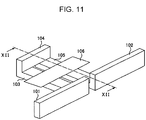
- Fig. 11 illustrates a configuration of a current sensor disclosed in PTL 1.
- Fig. 12 is a cross-sectional view taken along line XII-XII of Fig. 12 .
- a U shape is formed by using plate-like conductors 103, 104, and 105 disposed between two plate-like conductors 101 and 102 running straight, and a sensor board 106 is disposed above the U-shaped portion.
- a current detecting device unit 107 including magnetoresistance effect elements is disposed on the sensor board 106.
- the dotted line, to which an arrow is attached in Fig. 12 indicates the center of the distribution of a current to be measured Is.
- the current to be measured Is flows from one to the other of the two plate-like conductors 103 and 105, each of which runs like an arm, via the plate-like conductor 104. Even if the plate-like conductor 104, which is bent upward, is long in the upward direction, the center of the substantial current distribution CP of the current to be measured Is stays at a lower position, as illustrated in Fig. 12 , because the current to be measured Is tends to flow along the shortest path.
- the center of a magnetic field Hs due to the current to be measured Is flowing through the plate-like conductor 104 is located lower than the level at which the magnetic field Hs is perpendicular to the bias magnetic field for the magnetoresistance effect elements (the level indicated by the dot-dashed line in Fig. 12 ), and the difficulty that the magnetic field Hs affects the sensitivity of the magnetoresistance effect elements arises.
- the present invention is provided in view of the foregoing situation, and an object of the present invention is to provide a current sensor that can reduce an effect that is exerted on measurement sensitivity by the magnetic field due to a current to be measured flowing along a bent path.
- a current sensor includes a conductor through which a current to be measured flows and a magnetoresistance effect element located on a first imaginary flat plane that is parallel to a first imaginary straight line and a second imaginary straight line.
- the conductor includes a first conductor portion that runs along the first imaginary straight line and that is separated from the first imaginary flat plane, and through which the current to be measured flows parallel to the first imaginary straight line, a second conductor portion that runs along the second imaginary straight line and that intersects the first imaginary flat plane, and through which the current to be measured flows parallel to the second imaginary straight line, a bent portion that is disposed along a current path between the second conductor portion and the first conductor portion and that is bent in a first direction parallel to the first imaginary straight line from a second direction parallel to the second imaginary straight line, and a third conductor portion that is disposed along a current path between the bent portion and the first conductor portion.
- the magnetoresistance effect element detects a magnetic field due to the current to be measured flowing through the first conductor portion.
- the direction of a magnetic field to which the magnetoresistance effect element has sensitivity and the direction of a magnetic field by which the sensitivity of the magnetoresistance effect element is influenced are parallel to the first imaginary flat plane, and the third conductor portion intersects the first imaginary flat plane.
- the magnetoresistance effect element which detects the magnetic field due to the current to be measured flowing through the first conductor portion, is located on the first imaginary flat plane, and the second conductor portion intersects the first imaginary flat plane. Further, after bending at the bent portion and heading in the first direction parallel to the first imaginary straight line, the current to be measured flows through the first conductor portion via the third conductor portion, which intersects the first imaginary flat plane. Consequently, the center of the distribution of the current to be measured, which is separated from the first imaginary flat plane in the first conductor portion, can reach the vicinity of the first imaginary flat plane by passing through the third conductor portion.
- the flow of the current to be measured is centered around the first imaginary flat plane in the second conductor portion.
- the magnetic field due to the current to be measured flowing through the second conductor portion is oriented to the direction perpendicular to the first imaginary flat plane, the direction being substantially perpendicular to the direction of the magnetic field that affects the sensitivity of the magnetoresistance effect element. Accordingly, the magnetic field due to the current to be measured flowing through the second conductor portion is unlikely to affect the sensitivity of the magnetoresistance effect element.
- the third conductor portion may be located on a second imaginary flat plane that is perpendicular to the first imaginary flat plane and that contains the first imaginary straight line, and the current to be measured may flow parallel to the second imaginary flat plane through the third conductor portion.
- the third conductor portion contains the first imaginary straight line and crosses the first imaginary flat plane at right angles, the path of the current to be measured in the third conductor portion is shortened.
- the cross section perpendicular to the second direction at a portion connecting the bent portion and the second conductor portion, the cross section perpendicular to the first direction at a portion connecting the bent portion and the third conductor portion, and the cross section of the second conductor portion, the cross section being perpendicular to the second direction may be equal to each other in shape and size and uniform, and the width of the bent portion and the width of the second conductor portion in a third direction perpendicular to the first imaginary flat plane may be equal to each other and uniform.
- This configuration facilitates processing of bending the conductor at the bent portion, and process accuracy is improved. Further, the current to be measured, which bends to the second conductor portion at the bent portion, is likely to flow parallel to the second imaginary straight line.
- the edge that is entirely separated from the first imaginary flat plane is referred to as a first edge, and the first edge may be closer to the first imaginary flat plane in the bent portion and in the second conductor portion than in the first conductor portion.
- the width of the bent portion and the width of the second conductor portion in the third direction are narrow.
- This configuration causes the center of the distribution of the current to be measured flowing through the second conductor portion to lie in an appropriate region around the first imaginary flat plane, and thus the direction of the magnetic field due to the current to be measured flowing through the second conductor portion is likely to cross the first imaginary flat plane at right angles.
- a distance between a point on the first edge of the third conductor portion and the first edge of the bent portion in the third direction may decrease as the point approaches the bent portion.
- the edge having a portion intersecting the first imaginary flat plane is referred to as a second edge, and a distance between a point on the second edge of the third conductor portion and the second edge of the bent portion in the third direction may decrease as the point approaches the bent portion.
- the conductor may have a plane symmetrical form about a third imaginary flat plane that passes through the center of the second conductor portion and that is perpendicular to the first imaginary flat plane, and each of the bent portion, the third conductor portion, and the first conductor portion may have two parts arranged symmetrically about the third imaginary flat plane.
- the current sensor described above may include at least one pair of the magnetoresistance effect elements disposed symmetrically about the third imaginary flat plane.
- the pair of the magnetoresistance effect elements detects a symmetrical magnetic field due to the current to be measured.
- the at least one pair of the magnetoresistance effect elements may be contained in a package, and the package may be disposed between the two parts of the first conductor portion when viewed in the direction perpendicular to the first imaginary flat plane.
- the device can be downsized by using this configuration.
- the conductor may be bent at an obtuse angle at the bent portion.
- This configuration facilitates processing of bending the conductor at the bent portion, and process accuracy is improved.
- an effect that is exerted on measurement sensitivity by the magnetic field due to a current to be measured flowing along a bent path can be reduced.
- Fig. 1 illustrates an example configuration of a current sensor according to a first embodiment of the present invention.
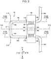
- Fig. 2 is a plan view of the current sensor illustrated in Fig. 1 when viewed from the Z1 side.
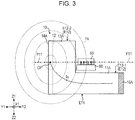
- Fig. 3 is a front view of the current sensor illustrated in Fig. 1 when viewed from the X2 side.
- X three directions perpendicular to each other are denoted by "X", "Y", and "Z”.
- Opposite directions in the X direction are denoted by "X1” and "X2”
- opposite directions in the Y direction are denoted by "Y1" and “Y2”
- opposite directions in the Z direction are denoted by "Z1" and "Z2”.
- the current sensor illustrated in Fig. 1 includes a conductor 10 made of metal or the like, a magnetic sensor 50 including magnetoresistance effect elements M1 to M4 that detect the magnetic field due to a current to be measured Is flowing through the conductor 10, and a circuit board 60 on which the magnetic sensor 50 is mounted.
- the conductor 10 and the circuit board 60 are fixed to each other by using an insulating support member (such as a mold member made of resin), which is not illustrated.
- the conductor 10 is a bent plate-like member.
- a plate-like material shaped by using processing such as blanking is subjected to bending processing, and the conductor 10 is formed.
- the conductor 10 is bent into a U shape as illustrated in Fig. 2 and has a plane symmetrical form about a third imaginary flat plane P13, which is parallel to the Y direction and the Z direction.
- the conductor 10 has a first conductor portion 11A and a first conductor portion 11B, which are the two arms of the U-shaped bent form.
- the first conductor portion 11A runs along a first imaginary straight line L11A, which is parallel to the Y direction
- the first conductor portion 11B runs along a first imaginary straight line L11B, which is parallel to the Y direction.
- the first conductor portion 11A and the first conductor portion 11B have a belt-like form that is thin in the X direction and that has an approximately uniform width in the Z direction.
- the first conductor portion 11A and the first conductor portion 11B are portions that are symmetrical to each other about the third imaginary flat plane P13. In the plan view in Fig.
- the first conductor portion 11A is located on the X2 side, and the first conductor portion 11B is located on the X1 side.
- the current to be measured Is flows parallel to the first imaginary straight line L11A in the first conductor portion 11A and flows parallel to the first imaginary straight line L11B in the first conductor portion 11B.
- the conductor 10 has a second conductor portion 12, which forms the bottom part of the U-shaped bent form.
- the second conductor portion 12 runs along a second imaginary straight line L12, which is parallel to the X direction.
- the second conductor portion 12 has a belt-like form that is thin in the Y direction and that has an approximately uniform width in the Z direction.
- the second conductor portion 12 is wider than the first conductor portion 11A and the first conductor portion 11B in the Z direction.
- the third imaginary flat plane P13 passes through the center of the second conductor portion 12 in the X direction.
- a first imaginary flat plane P11 is defined and located between the second imaginary straight line L12 and each of the first imaginary straight lines L11A and L11B.
- the first imaginary flat plane P11 is parallel to the first imaginary straight lines L11A and L11B and to the second imaginary straight line L12 (that is, parallel to the X direction and to the Y direction).
- the Z direction is perpendicular to the first imaginary flat plane P11 and corresponds to a third direction in the present invention.
- the first conductor portion 11A and the first conductor portion 11B are separated from the first imaginary flat plane P11, and the second conductor portion 12 intersects the first imaginary flat plane P11.
- the angle between the first imaginary straight line L11A and the second imaginary straight line L12 and the angle between the first imaginary straight line L11B and the second imaginary straight line L12 are not necessarily equal to a right angle, as described below. However, neither the first imaginary straight line L11A nor the first imaginary straight line L11B is parallel to the second imaginary straight line L12.
- the conductor 10 has a first bent portion 14A along the current path between the second conductor portion 12 and the first conductor portion 11A and has a first bent portion 14B along the current path between the second conductor portion 12 and the first conductor portion 11B.
- the first bent portion 14A bends in the Y2 direction (a first direction parallel to the first imaginary straight line L11A) from the X2 direction (a second direction parallel to the second imaginary straight line L12) at a substantially right angle
- the first bent portion 14B bends in the Y2 direction (the first direction, which is parallel to the first imaginary straight line L11B) from the X1 direction (a second direction parallel to the second imaginary straight line L12) at a substantially right angle.
- the width of the first bent portion 14A and the width of the first bent portion 14B in the Z direction are uniform and are equal to the width of the second conductor portion 12.
- the first bent portion 14A and the first bent portion 14B are portions that are symmetrical to each other about the third imaginary flat plane P13.
- the first bent portion 14A and the first bent portion 14B are an example bent portion in the present invention.
- the conductor 10 has a third conductor portion 13A along the current path between the first bent portion 14A and the first conductor portion 11A and has a third conductor portion 13B along the current path between the first bent portion 14B and the first conductor portion 11B.
- Each of the third conductor portion 13A and the third conductor portion 13B intersects the first imaginary flat plane P11.
- the third conductor portion 13A runs along a second imaginary flat plane P12A, which is perpendicular to the first imaginary flat plane P11 and contains the first imaginary straight line L11A.
- the third conductor portion 33B runs along a second imaginary flat plane P12B, which is perpendicular to the first imaginary flat plane P11 and contains the first imaginary straight line L11B.
- the current to be measured Is flows parallel to the second imaginary flat plane P12A in the third conductor portion 13A.
- the current to be measured Is flows parallel to the second imaginary flat plane P12B in the third conductor portion 13B.
- the third conductor portion 13A and the third conductor portion 13B are thin in the X direction and have a uniform width in the Z direction.
- the width of the third conductor portion 13A and the width of the third conductor portion 13B in the Z direction are equal to the width of the first bent portion 14A, the width of the first bent portion 14B, and the width of the second conductor portion 12.
- the conductor 10 has a cross section that is equal in shape and size and uniform in the portion ranging from the second conductor portion 12 to the third conductor portion 13A.
- the cross section perpendicular to the X direction at the portion connecting the second conductor portion 12 and the first bent portion 14A, the cross section perpendicular to the Y direction at the portion connecting the first bent portion 14A and the third conductor portion 13A, and the cross section of the second conductor portion 12, the cross section being perpendicular to the X direction are equal to each other in shape and size and uniform and all have a rectangular shape elongated in the Z direction.
- the conductor 10 also has a cross section that is equal in shape and size and uniform in the portion ranging from the second conductor portion 12 to the third conductor portion 13B.
- the conductor 10 has a fourth conductor portion 16A and a fourth conductor portion 16B, through which the current to be measured Is is input to and output from the U-shaped bent portion.
- the fourth conductor portion 16A and the fourth conductor portion 16B have a belt-like form that is thin in the Y direction and that has a uniform height in the Z direction, and each run in the X direction.
- the fourth conductor portion 16A is connected to the first conductor portion 11A via a second bent portion 15A
- the fourth conductor portion 16B is connected to the first conductor portion 11B via a second bent portion 15B.
- the magnetic sensor 50 is a packaged integrated circuit (IC), in which magnetoresistance effect elements M1 to M4, such as GMR elements and AMR elements, are included.
- the magnetoresistance effect elements M1 and M3 are paired and disposed symmetrically about the third imaginary flat plane P13
- the magnetoresistance effect elements M2 and M4 are paired and disposed symmetrically about the third imaginary flat plane P13.
- the magnetoresistance effect elements M1 and M2 are disposed on the X2 side and detect the magnetic field due to the current to be measured Is flowing through the first conductor portion 11A.
- the magnetoresistance effect elements M3 and M4 are disposed on the X1 side and detect the magnetic field due to the current to be measured Is flowing through the first conductor portion 11B.
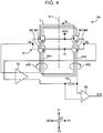
- Fig. 4 illustrates an example configuration of the magnetic sensor 50.
- the magnetic sensor 50 which is illustrated in the example in Fig. 4 , includes a bridge circuit 51 in which the magnetoresistance effect elements M1 to M4 are included, a coil L, a coil driver circuit 52, a differential amplifier 53, and a resistor Rs.
- One end of the magnetoresistance effect element M1 is connected to a power supply voltage VDD, the other end of the magnetoresistance effect element M1 is connected to one end of the magnetoresistance effect element M2, and the other end of the magnetoresistance effect element M2 is grounded.
- One end of the magnetoresistance effect element M3 is connected to the power supply voltage VDD, the other end of the magnetoresistance effect element M3 is connected to one end of the magnetoresistance effect element M4, and the other end of the magnetoresistance effect element M4 is grounded.
- a voltage Va is generated at the node between the magnetoresistance effect elements M1 and M2, and a voltage Vb is generated at the node between the magnetoresistance effect elements M3 and M4.
- Fig. 4 white arrows indicate the sensitivity directions of the magnetoresistance effect elements, and black arrows indicate the influence-on-sensitivity directions of the magnetoresistance effect elements.
- the magnetoresistance effect elements M1 and M3 have the sensitivity direction in the X1 direction and the influence-on-sensitivity direction in the Y1 direction.
- the magnetoresistance effect elements M2 and M4 have the sensitivity direction in the X2 direction and the influence-on-sensitivity direction in the Y2 direction.
- the resistance of each of the magnetoresistance effect elements M1 to M4 decreases as the magnetic field in the sensitivity direction increases and increases as the magnetic field in the sensitivity direction decreases.
- the coil L generates magnetic fields to cancel out the magnetic fields in the X direction that are induced at positions of the magnetoresistance effect elements M1 to M4 by the current to be measured Is in the first conductor portion 11A and in the first conductor portion 11B.
- the coil L produces a current path CP1 running in the Y direction in the vicinity of the magnetoresistance effect elements M1 and M2.
- a current Ib flows in the Y2 direction along the current path CP1
- a magnetic field H51 is generated in the X2 direction in the vicinity of the magnetoresistance effect elements M1 and M2.
- the magnetic field H51 cancels out the components in the X1 direction of the magnetic fields that are induced at the positions of the magnetoresistance effect elements M1 and M2 by the current to be measured Is in the first conductor portion 11A.
- the coil L produces a current path CP2 running in the Y direction in the vicinity of the magnetoresistance effect elements M3 and M4.
- a magnetic field H52 is generated in the X1 direction in the vicinity of the magnetoresistance effect elements M3 and M4.
- the magnetic field H52 cancels out the components in the X2 direction of the magnetic fields that are induced at the positions of the magnetoresistance effect elements M3 and M4 by the current to be measured Is in the first conductor portion 11B.
- the coil driver circuit 52 passes the current Ib through the coil L in accordance with the difference between the voltages Va and Vb of the bridge circuit 51.
- the magnetoresistance effect elements M1 to M4 are assumed to have approximately equal resistances. In this case, when the current to be measured Is becomes null, the voltages Va and Vb become approximately equal.
- the current to be measured Is flows from the fourth conductor portion 16A to the fourth conductor portion 16B, the magnetic field in the X direction due to the current to be measured Is causes the resistances of the magnetoresistance effect elements M1 to M4 to change, and the voltage Va exceeds the voltage Vb.
- the coil driver circuit 52 outputs the current Ib so that the current Ib flows in the Y2 direction along the current path CP1 and flows in the Y1 direction along the current path CP2.
- the coil driver circuit 52 increases the current Ib as the difference between the voltages Va and Vb increases.
- the magnetic field in the Y direction induced by the current Ib of the coil L exerts an effect to cancel out the component in the X direction of the magnetic field induced by the current to be measured Is.
- an increase in the voltage Va relative to the voltage Vb is prevented or reduced.
- the coil driver circuit 52 outputs the current Ib so that the current Ib flows in the Y1 direction along the current path CP1 and flows in the Y2 direction along the current path CP2.
- the coil driver circuit 52 increases the current Ib as the difference between the voltages Va and Vb increases.
- the magnetic field in the X direction induced by the current Ib of the coil L exerts an effect to cancel out the component in the Y direction of the magnetic field induced by the current to be measured Is.
- a decrease in the voltage Va relative to the voltage Vb is prevented or reduced.
- the coil driver circuit 52 has a sufficiently large gain, which is the ratio of the current Ib that is output to the coil L to the voltage (Va - Vb) that is input from the bridge circuit 51.
- the voltages Va and Vb of the bridge circuit 51 become approximately equal because of feedback operation. Consequently, the component in the X direction of the magnetic field due to the current to be measured Is and the magnetic field in the X direction due to the current Ib of the coil L are approximately equal at each of the positions of the magnetoresistance effect elements M1 to M4.
- the resistor Rs is inserted in the current path of the coil L.
- the differential amplifier 53 amplifies a voltage that is generated between both ends of the resistor Rs by the current Ib flowing through the coil L and outputs the amplified voltage as a detection signal S12.
- the detection signal S12 is a signal proportional to the current Ib flowing through the coil L and is substantially proportional to the magnetic field due to the coil L. Since the magnetic field due to the coil L is controlled so as to cancel out the component in the X direction of the magnetic field that is exerted on the magnetoresistance effect elements M1 to M4 by the current to be measured Is, the magnetic field due to the coil L is substantially proportional to the current to be measured Is. Thus, the detection signal S12 is a signal substantially proportional to the current to be measured Is.
- the dotted line to which an arrow is attached in Fig. 3 indicates the center of the distribution of the current to be measured Is.
- the center of the distribution of the current to be measured Is is located on the Z2 side of the first imaginary flat plane P11 in the first conductor portion 11A.
- the center of the distribution of the current to be measured Is shifts in the Z1 direction.
- the center of the distribution CP of the current to be measured Is flowing from the first bent portion 14A to the second conductor portion 12 is substantially in the first imaginary flat plane P11.
- the magnetoresistance effect elements M1 to M4 which detect the magnetic field due to the current to be measured IS flowing through the first conductor portions 11A and 11B, are located on the first imaginary flat plane P11, and the second conductor portion 12 intersects the first imaginary flat plane P11.
- the current to be measured Is which bends in the Y direction at the first bent portions 14A and 14B, flows through the first conductor portions 11A and 11B via the third conductor portions 13A and 13B, which intersect the first imaginary flat plane P11.
- the center of the distribution of the current to be measured Is which is separated from the first imaginary flat plane P11 in the first conductor portions 11A and 11B, passes through the third conductor portions 13A and 13B and thus reaches the vicinity of the first imaginary flat plane P11. Since the center of the distribution of the current to be measured Is reaches the vicinity of the first imaginary flat plane P11 in the third conductor portions 13A and 13B, the flow of the current to be measured Is, which bends at the first bent portions 14A and 14B, is centered around the first imaginary flat plane P11 in the second conductor portion 12.
- the direction of the magnetic field Hs due to the current to be measured Is flowing through the second conductor portion 12 is perpendicular to the first imaginary flat plane P11 and substantially perpendicular to the influence-on-sensitivity directions of the magnetoresistance effect elements M1 to M4. Accordingly, the magnetic field due to the current to be measured Is flowing through the second conductor portion 12 is unlikely to affect the sensitivity of the magnetoresistance effect elements M1 to M4. In summary, the effect that is exerted on the measurement sensitivity by the magnetic field Hs due to the current to be measured Is flowing along the bent path can effectively be reduced.
- the third conductor portion 13A runs along the second imaginary flat plane P12A, which is perpendicular to the first imaginary flat plane P11 and contains the first imaginary straight line L11A, and the current to be measured Is flows parallel to the second imaginary flat plane P12A in the third conductor portion 13A.
- the resistance of the third conductor portion 13A is reduced.
- the third conductor portion 13B which is a symmetrical portion to the third conductor portion 13A. Consequently, the resistance of the conductor 10 is reduced, and the loss due to the resistance can be reduced.
- the cross section perpendicular to the X direction at the portion connecting the second conductor portion 12 and the first bent portion 14A, the cross section perpendicular to the Y direction at the portion connecting the first bent portion 14A and the third conductor portion 13A, and the cross section of the second conductor portion 12, the cross section being perpendicular to the X direction are equal to each other in shape and size and uniform.
- the conductor 10 similarly to the above description, also has a cross section that is equal in shape and size and uniform in the portion ranging from the second conductor portion 12 to the third conductor portion 13A. This configuration facilitates processing of bending the conductor 10 at the first bent portions 14A and 14B, and process accuracy is improved.
- the current to be measured Is which bends to the second conductor portion 12 at the first bent portions 14A and 14B, is likely to flow parallel to the second imaginary straight line L12 (in the X direction). Consequently, as the direction of the magnetic field Hs is likely to be parallel to the direction perpendicular to the first imaginary flat plane P11 (in the Z direction), the effect that is exerted on the measurement sensitivity by the magnetic field Hs can be reduced more effectively.
- the magnetoresistance effect elements M1 to M4 are contained in an IC package of the magnetic sensor 50, and the IC package of the magnetic sensor 50 is disposed between the first conductor portion 11A and the first conductor portion 11B when viewed in the Z direction.
- a current sensor can be downsized by using this configuration.
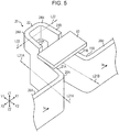
- FIG. 5 illustrates an example configuration of a current sensor according to the second embodiment of the present invention.
- Fig. 6 is a plan view of the current sensor illustrated in Fig. 5 when viewed from the Z1 side.
- Fig. 7 is a front view of the current sensor illustrated in Fig. 5 when viewed from the X2 side.
- a circuit board 60 is omitted from the illustration.
- the current sensor according to the second embodiment includes a magnetic sensor 50 and the circuit board 60, which are similar to those included in the current sensor according to the first embodiment, and a conductor 20.
- the conductor 20 is formed by bending a plate-like material into a U shape and has a plane symmetrical form.
- the conductor 10 and the conductor 20 have many features in common, and different features are mainly described below.
- the first conductor portion 11A, the first conductor portion 11B, the second conductor portion 12, the third conductor portion 13A, the third conductor portion 13B, the first bent portion 14A, the first bent portion 14B, the second bent portion 15A, the second bent portion 15B, the fourth conductor portion 16A, and the fourth conductor portion 16B in the conductor 10 correspond to a first conductor portion 21A, a first conductor portion 21B, a second conductor portion 22, a third conductor portion 23A, a third conductor portion 23B, a first bent portion 24A, a first bent portion 24B, a second bent portion 25A, a second bent portion 25B, a fourth conductor portion 26A, and a fourth conductor portion 26B, respectively, in the conductor 20.
- each portion in the conductor 20 denoted by a numeral corresponds to a portion in the conductor 10 denoted by a numeral whose tens digit is changed from "2" to "1".
- a first imaginary straight line L21A, a first imaginary straight line L21B, a second imaginary straight line L22, a first imaginary flat plane P21, a second imaginary flat plane P22A, a second imaginary flat plane P22B, and a third imaginary flat plane P23 in Figs. 5 to 7 correspond to the first imaginary straight line L11A, the first imaginary straight line L11B, the second imaginary straight line L12, the first imaginary flat plane P11, the second imaginary flat plane P12A, the second imaginary flat plane P12B, and the third imaginary flat plane P13, respectively, in Figs. 1 to 3 .
- each imaginary straight line or each imaginary flat plane in Fig. 5 to 7 denoted by a numeral corresponds to an imaginary straight line or an imaginary flat plane in Figs. 1 to 3 denoted by a numeral whose tens digit is changed from "2" to "1".
- the magnetic sensor 50 is disposed on the Z1 side surface of the circuit board 60, as illustrated in Fig. 1 , but, in the current sensor according to the second embodiment, the magnetic sensor 50 is disposed on the Z2 side surface of the circuit board 60, as illustrated in Fig. 7 .
- bending angles at the first bent portions 14A and 14B are approximately a right angle, as illustrated in Fig. 2
- bending angles at the first bent portions 24A and 24B are an obtuse angle slightly larger than a right angle, as illustrated in Fig. 6 , in the current sensor according to the second embodiment.
- FIG. 1 A comparison between Fig. 1 and Fig. 5 reveals that the width of the second conductor portion 22, the width of the first bent portion 24A, and the width of the first bent portion 24B in the Z direction in the current sensor according to the second embodiment are narrower than the width of the second conductor portion 12, the width of the first bent portion 14A, and the width of the first bent portion 14B in the Z direction in the current sensor according to the first embodiment.
- the conductor 10 in the current sensor according to the first embodiment has two edges (a first edge E11 and a second edge E12) separated from each other in the Z direction.
- the first edge E11 is an edge entirely separated from the first imaginary flat plane P11
- the second edge E12 is an edge having a portion that intersects the first imaginary flat plane P11.
- the second edge E12 crosses the first imaginary flat plane P11 between the second edge E12-1 of the first conductor portion and the second edge E12-2 of the second conductor portion.
- the conductor 20 in the current sensor according to the second embodiment has two edges (a first edge E21 and a second edge E22) separated from each other in the Z direction.
- the first edge E21 is an edge separated from the first imaginary flat plane P21
- the second edge E22 is an edge that intersects the first imaginary flat plane P21.
- FIG. 3 A comparison between Fig. 3 and Fig. 7 reveals that, while the first edge E11 in the conductor 10 has every portion located at the same position in the Z direction, the second edge E22 of the first conductor portions 21A and 21B and the second edge E22 of the first bent portion 24A, the first bent portion 24B, and the second conductor portion 22 are located at different positions in the Z direction in the conductor 20. Specifically, the first edge E21 (E21-3) of the first bent portion 24A, the first bent portion 24B, and the second conductor portion 22 is located closer than the first edge E21 (E21-1) of the first conductor portions 21A and 21B to the first imaginary flat plane P21. Such a difference in the edge position leads to narrower widths of the second conductor portion 22, the first bent portion 24A, and the first bent portion 24B in the Z direction in the current sensor according to the second embodiment.
- the width of the first bent portion 24A, the width of the first bent portion 24B, and the width of the second conductor portion 22 in the Z direction are narrower.
- the magnetic field Hs due to the current to be measured Is flowing through the second conductor portion 22 is likely to cross the first imaginary flat plane P21 at right angles.
- the narrower widths of the first bent portion 24A, the first bent portion 24B, and the second conductor portion 22 in the Z direction cause the position of the first imaginary flat plane P21 to shift in the Z1 direction. Consequently, as revealed by a comparison between Fig. 3 and Fig. 7 , the widths of the first conductor portions 21A and 21B in the Z direction relative to the width of the conductor 20 as a whole in the Z direction can be increased. Accordingly, the resistance of the conductor 20 can be reduced.
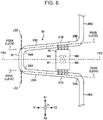
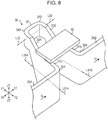
- Fig. 8 illustrates an example configuration of a current sensor according to the third embodiment of the present invention.
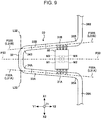
- Fig. 9 is a plan view of the current sensor illustrated in Fig. 8 when viewed from the Z1 side.
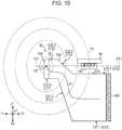
- Fig. 10 is a front view of the current sensor illustrated in Fig. 8 when viewed from the X2 side.
- a circuit board 60 is omitted from the illustration.
- the current sensor according to the third embodiment includes a magnetic sensor 50 and the circuit board 60, which are similar to those included in the current sensor according to the second embodiment, and a conductor 30.
- the conductor 30 is formed by bending a plate-like material into a U shape and has a plane symmetrical form.
- the conductor 20 and the conductor 30 have many features in common, and different features are mainly described below.
- the first conductor portion 21A, the first conductor portion 21B, the second conductor portion 22, the third conductor portion 23A, the third conductor portion 23B, the first bent portion 24A, the first bent portion 24B, the second bent portion 25A, the second bent portion 25B, the fourth conductor portion 26A, and the fourth conductor portion 26B in the conductor 20 correspond to a first conductor portion 31A, a first conductor portion 31B, a second conductor portion 32, a third conductor portion 33A, a third conductor portion 33B, a first bent portion 34A, a first bent portion 34B, a second bent portion 35A, a second bent portion 35B, a fourth conductor portion 36A, and a fourth conductor portion 36B, respectively, in the conductor 30.
- each portion in the conductor 30 denoted by a numeral corresponds to a portion in the conductor 20 denoted by a numeral whose tens digit is changed from "3" to "2".
- a first imaginary straight line L31A, a first imaginary straight line L31B, a second imaginary straight line L32, a first imaginary flat plane P31, a second imaginary flat plane P32A, a second imaginary flat plane P32B, and a third imaginary flat plane P33 in Figs. 8 to 10 correspond to the first imaginary straight line L21A, the first imaginary straight line L21B, the second imaginary straight line L22, the first imaginary flat plane P21, the second imaginary flat plane P22A, the second imaginary flat plane P22B, and the third imaginary flat plane P23, respectively, in Figs. 5 to 7 .
- each imaginary straight line or each imaginary flat plane in Fig. 8 to 10 denoted by a numeral corresponds to an imaginary straight line or an imaginary flat plane in Figs. 5 to 7 denoted by a numeral whose tens digit is changed from "3" to "2".
- the edge position in the Z direction changes discontinuously at the first edge E21-2 of the third conductor portions 23A and 23B, but, in the current sensor according to the third embodiment, as illustrated in Fig. 10 , the edge position in the Z direction changes continuously in the first edge E31-2 of the third conductor portions 33A and 33B. Specifically, the distance between a point on the first edge E31-2 of the third conductor portions 33A and 33B and the first edge E31-3 of the first bent portions 34A and 34B in the Z direction decreases as the point approaches the first bent portions 34A and 34B.
- FIG. 7 A comparison between Fig. 7 and Fig. 10 reveals that the corner on the Z2 side and on the Y1 side where the amount of current is considered to be relatively small in the distribution of the current to be measured Is in the third conductor portions 23A and 23B is cut for the third conductor portions 33A and 33B. Consequently, the amount of material used for the conductor 10 can be reduced without significantly increasing the resistance of the conductor 10, which leads to weight reduction of a device.
- the edge position in the Z direction changes discontinuously at the second edge E22-2 of the third conductor portions 23A and 23B, but, in the current sensor according to the third embodiment, as illustrated in Fig. 10 , the edge position in the Z direction changes continuously in the second edge E32-2 of the third conductor portions 33A and 33B. Specifically, the distance between a point on the second edge E32-2 of the third conductor portions 33A and 33B and the second edge E32-3 of the first bent portions 34A and 34B in the Z direction decreases as the point approaches the first bent portions 34A and 34B.
- FIG. 7 A comparison between Fig. 7 and Fig. 10 reveals that the corner on the Z1 side and on the Y2 side where the amount of current is considered to be relatively small in the distribution of the current to be measured Is in the third conductor portions 23A and 23B is cut for the third conductor portions 33A and 33B. Consequently, the amount of material used for the conductor 10 can be reduced without significantly increasing the resistance of the conductor 10, which leads to weight reduction of a device.
- the edge positions of the first edge E31-2 and the second edge E32-2 continuously change in the Z direction, but the present invention is not limited to this example.
- a point on the edges of the third conductor portions may change the position in the Z direction in a stepwise manner as the point approaches the bent portions.
- the configuration of the magnetic sensor is not limited to the full bridge circuit of the magnetoresistance effect elements illustrated in Fig. 4 , and, for example, a half bridge circuit using two magnetoresistance effect elements may be adopted.
- any number of bent portions may be adopted in the present invention, and the present invention may be applied, for example, to a case where only one bent portion is adopted.
Landscapes
- Physics & Mathematics (AREA)
- General Physics & Mathematics (AREA)
- Condensed Matter Physics & Semiconductors (AREA)
- Measuring Instrument Details And Bridges, And Automatic Balancing Devices (AREA)
- Measuring Magnetic Variables (AREA)
Abstract
Description
- The present invention relates to a current sensor that measures a current by using a magneto-electric resistance effect element, such as a giant magnetoresistance (GMR) element or an anisotropic magnetoresistance (AMR) element.
- Differential-type current sensors configured to obtain a detection result of a current in accordance with differences between outputs from magnetic sensors are known in the art. Magnetic sensors detect magnetic fields due to currents flowing in opposite directions through a busbar bent into a U shape.
- A magneto-electric resistance effect element, such as a GMR element or an AMR element, has a direction (sensitivity direction) of a magnetic field that causes a change in the resistance and a direction (influence-on-sensitivity direction) of a magnetic field that affects the detection sensitivity. The influence-on-sensitivity direction typically coincides with the direction of an internal bias magnetic field and is perpendicular to the sensitivity direction. If a magnetic field is applied from outside in the influence-on-sensitivity direction, the sensitivity changes because application of a magnetic field is equivalent to a change in the bias magnetic field. In the case of a differential-type current sensor described above, a magnetic field induced by a current flowing through a bottom part of a U-shaped portion has a component perpendicular to the sensitivity direction and thus affects the sensitivity of a magnetoresistance effect element.
- Accordingly, the bottom part of the U-shaped portion of a current sensor illustrated in Fig. 13 in PTL 1 is subjected to bending processing. Because of this bending processing, the line connecting the center of the magnetic field due to a current flowing through the bottom part and the point where the magnetic field crosses a bias magnetic field for the magnetoresistance effect elements at right angles is likely to run in the direction of the bias magnetic field. Consequently, the magnetic field due to a current flowing through the bottom part is likely to cross the bias magnetic field at right angles, and the effect on the sensitivity is reduced.
-
- PTL 1: Japanese Unexamined Patent Application Publication No.
2011-39021 - PTL 2: Japanese Unexamined Patent Application Publication No.
2015-152418 -
Fig. 11 illustrates a configuration of a current sensor disclosed in PTL 1.Fig. 12 is a cross-sectional view taken along line XII-XII ofFig. 12 . A U shape is formed by using plate-like conductors like conductors sensor board 106 is disposed above the U-shaped portion. A currentdetecting device unit 107 including magnetoresistance effect elements is disposed on thesensor board 106. - The dotted line, to which an arrow is attached in
Fig. 12 , indicates the center of the distribution of a current to be measured Is. The current to be measured Is flows from one to the other of the two plate-like conductors like conductor 104. Even if the plate-like conductor 104, which is bent upward, is long in the upward direction, the center of the substantial current distribution CP of the current to be measured Is stays at a lower position, as illustrated inFig. 12 , because the current to be measured Is tends to flow along the shortest path. Thus, the center of a magnetic field Hs due to the current to be measured Is flowing through the plate-like conductor 104 (the center of the magnetic field Hs being the center of the current distribution CP) is located lower than the level at which the magnetic field Hs is perpendicular to the bias magnetic field for the magnetoresistance effect elements (the level indicated by the dot-dashed line inFig. 12 ), and the difficulty that the magnetic field Hs affects the sensitivity of the magnetoresistance effect elements arises. - The present invention is provided in view of the foregoing situation, and an object of the present invention is to provide a current sensor that can reduce an effect that is exerted on measurement sensitivity by the magnetic field due to a current to be measured flowing along a bent path.
- A current sensor according to the present invention includes a conductor through which a current to be measured flows and a magnetoresistance effect element located on a first imaginary flat plane that is parallel to a first imaginary straight line and a second imaginary straight line. The conductor includes a first conductor portion that runs along the first imaginary straight line and that is separated from the first imaginary flat plane, and through which the current to be measured flows parallel to the first imaginary straight line, a second conductor portion that runs along the second imaginary straight line and that intersects the first imaginary flat plane, and through which the current to be measured flows parallel to the second imaginary straight line, a bent portion that is disposed along a current path between the second conductor portion and the first conductor portion and that is bent in a first direction parallel to the first imaginary straight line from a second direction parallel to the second imaginary straight line, and a third conductor portion that is disposed along a current path between the bent portion and the first conductor portion. The magnetoresistance effect element detects a magnetic field due to the current to be measured flowing through the first conductor portion. The direction of a magnetic field to which the magnetoresistance effect element has sensitivity and the direction of a magnetic field by which the sensitivity of the magnetoresistance effect element is influenced are parallel to the first imaginary flat plane, and the third conductor portion intersects the first imaginary flat plane.
- In this configuration, while the first conductor portion is separated from the first imaginary flat plane, the magnetoresistance effect element, which detects the magnetic field due to the current to be measured flowing through the first conductor portion, is located on the first imaginary flat plane, and the second conductor portion intersects the first imaginary flat plane. Further, after bending at the bent portion and heading in the first direction parallel to the first imaginary straight line, the current to be measured flows through the first conductor portion via the third conductor portion, which intersects the first imaginary flat plane. Consequently, the center of the distribution of the current to be measured, which is separated from the first imaginary flat plane in the first conductor portion, can reach the vicinity of the first imaginary flat plane by passing through the third conductor portion. Since the center of the distribution of the current to be measured reaches the vicinity of the first imaginary flat plane after passing through the third conductor portion, the flow of the current to be measured, which bends at the bent portion, is centered around the first imaginary flat plane in the second conductor portion. In this configuration, the magnetic field due to the current to be measured flowing through the second conductor portion is oriented to the direction perpendicular to the first imaginary flat plane, the direction being substantially perpendicular to the direction of the magnetic field that affects the sensitivity of the magnetoresistance effect element. Accordingly, the magnetic field due to the current to be measured flowing through the second conductor portion is unlikely to affect the sensitivity of the magnetoresistance effect element.
- Preferably, the third conductor portion may be located on a second imaginary flat plane that is perpendicular to the first imaginary flat plane and that contains the first imaginary straight line, and the current to be measured may flow parallel to the second imaginary flat plane through the third conductor portion.
- In this configuration, since the third conductor portion contains the first imaginary straight line and crosses the first imaginary flat plane at right angles, the path of the current to be measured in the third conductor portion is shortened.
- Preferably, the cross section perpendicular to the second direction at a portion connecting the bent portion and the second conductor portion, the cross section perpendicular to the first direction at a portion connecting the bent portion and the third conductor portion, and the cross section of the second conductor portion, the cross section being perpendicular to the second direction, may be equal to each other in shape and size and uniform, and the width of the bent portion and the width of the second conductor portion in a third direction perpendicular to the first imaginary flat plane may be equal to each other and uniform.
- This configuration facilitates processing of bending the conductor at the bent portion, and process accuracy is improved. Further, the current to be measured, which bends to the second conductor portion at the bent portion, is likely to flow parallel to the second imaginary straight line.
- Preferably, of two edges of the conductor, which are separated in the third direction, the edge that is entirely separated from the first imaginary flat plane is referred to as a first edge, and the first edge may be closer to the first imaginary flat plane in the bent portion and in the second conductor portion than in the first conductor portion.
- In this configuration, the width of the bent portion and the width of the second conductor portion in the third direction are narrow. This configuration causes the center of the distribution of the current to be measured flowing through the second conductor portion to lie in an appropriate region around the first imaginary flat plane, and thus the direction of the magnetic field due to the current to be measured flowing through the second conductor portion is likely to cross the first imaginary flat plane at right angles.
- Preferably, a distance between a point on the first edge of the third conductor portion and the first edge of the bent portion in the third direction may decrease as the point approaches the bent portion.
- In this configuration, since the area of a region where the amount of current is relatively small in the distribution of the current to be measured in the third conductor portion is reduced, the amount of material to form the third conductor portion is reduced while an increase in the resistance is avoided or reduced.
- Preferably, of two edges of the conductor, which are separated in the third direction, the edge having a portion intersecting the first imaginary flat plane is referred to as a second edge, and a distance between a point on the second edge of the third conductor portion and the second edge of the bent portion in the third direction may decrease as the point approaches the bent portion.
- In this configuration, since the area of a region where the amount of current is relatively small in the distribution of the current to be measured in the third conductor portion is reduced, the amount of material to form the third conductor portion is reduced while an increase in the resistance is avoided or reduced.
- Preferably, the conductor may have a plane symmetrical form about a third imaginary flat plane that passes through the center of the second conductor portion and that is perpendicular to the first imaginary flat plane, and each of the bent portion, the third conductor portion, and the first conductor portion may have two parts arranged symmetrically about the third imaginary flat plane. The current sensor described above may include at least one pair of the magnetoresistance effect elements disposed symmetrically about the third imaginary flat plane.
- In this configuration, the pair of the magnetoresistance effect elements detects a symmetrical magnetic field due to the current to be measured.
- Preferably, the at least one pair of the magnetoresistance effect elements may be contained in a package, and the package may be disposed between the two parts of the first conductor portion when viewed in the direction perpendicular to the first imaginary flat plane.
- The device can be downsized by using this configuration.
- Preferably, the conductor may be bent at an obtuse angle at the bent portion.
- This configuration facilitates processing of bending the conductor at the bent portion, and process accuracy is improved.
- According to the present invention, an effect that is exerted on measurement sensitivity by the magnetic field due to a current to be measured flowing along a bent path can be reduced.
-
- [
Fig. 1] Fig. 1 illustrates an example configuration of a current sensor according to a first embodiment of the present invention. - [
Fig. 2] Fig. 2 is a plan view of the current sensor illustrated inFig. 1 . - [
Fig. 3] Fig. 3 is a front view of the current sensor illustrated inFig. 1 . - [
Fig. 4] Fig. 4 illustrates an example configuration of a magnetic sensor. - [
Fig. 5] Fig. 5 illustrates an example configuration of a current sensor according to a second embodiment of the present invention. - [
Fig. 6] Fig. 6 is a plan view of the current sensor illustrated inFig. 5 . - [
Fig. 7] Fig. 7 is a front view of the current sensor illustrated inFig. 5 . - [
Fig. 8] Fig. 8 illustrates an example configuration of a current sensor according to a third embodiment of the present invention. - [
Fig. 9] Fig. 9 is a plan view of the current sensor illustrated inFig. 8 . - [
Fig. 10] Fig. 10 is a front view of the current sensor illustrated inFig. 8 . - [
Fig. 11] Fig. 11 illustrates a configuration of a current sensor known in the related art. - [
Fig. 12] Fig. 12 is a cross-sectional view taken along line XII-XII ofFig. 11 . -
Fig. 1 illustrates an example configuration of a current sensor according to a first embodiment of the present invention.Fig. 2 is a plan view of the current sensor illustrated inFig. 1 when viewed from the Z1 side.Fig. 3 is a front view of the current sensor illustrated inFig. 1 when viewed from the X2 side. In the present specification, three directions perpendicular to each other are denoted by "X", "Y", and "Z". Opposite directions in the X direction are denoted by "X1" and "X2", opposite directions in the Y direction are denoted by "Y1" and "Y2", and opposite directions in the Z direction are denoted by "Z1" and "Z2". - The current sensor illustrated in
Fig. 1 includes aconductor 10 made of metal or the like, amagnetic sensor 50 including magnetoresistance effect elements M1 to M4 that detect the magnetic field due to a current to be measured Is flowing through theconductor 10, and acircuit board 60 on which themagnetic sensor 50 is mounted. Theconductor 10 and thecircuit board 60 are fixed to each other by using an insulating support member (such as a mold member made of resin), which is not illustrated. - The
conductor 10 is a bent plate-like member. For example, a plate-like material shaped by using processing such as blanking is subjected to bending processing, and theconductor 10 is formed. Theconductor 10 is bent into a U shape as illustrated inFig. 2 and has a plane symmetrical form about a third imaginary flat plane P13, which is parallel to the Y direction and the Z direction. - The
conductor 10 has afirst conductor portion 11A and afirst conductor portion 11B, which are the two arms of the U-shaped bent form. Thefirst conductor portion 11A runs along a first imaginary straight line L11A, which is parallel to the Y direction, and thefirst conductor portion 11B runs along a first imaginary straight line L11B, which is parallel to the Y direction. As illustrated inFig. 1 , thefirst conductor portion 11A and thefirst conductor portion 11B have a belt-like form that is thin in the X direction and that has an approximately uniform width in the Z direction. Thefirst conductor portion 11A and thefirst conductor portion 11B are portions that are symmetrical to each other about the third imaginary flat plane P13. In the plan view inFig. 2 , thefirst conductor portion 11A is located on the X2 side, and thefirst conductor portion 11B is located on the X1 side. The current to be measured Is flows parallel to the first imaginary straight line L11A in thefirst conductor portion 11A and flows parallel to the first imaginary straight line L11B in thefirst conductor portion 11B. - The
conductor 10 has asecond conductor portion 12, which forms the bottom part of the U-shaped bent form. Thesecond conductor portion 12 runs along a second imaginary straight line L12, which is parallel to the X direction. As illustrated inFig. 1 , thesecond conductor portion 12 has a belt-like form that is thin in the Y direction and that has an approximately uniform width in the Z direction. Thesecond conductor portion 12 is wider than thefirst conductor portion 11A and thefirst conductor portion 11B in the Z direction. As illustrated inFig. 2 , the third imaginary flat plane P13 passes through the center of thesecond conductor portion 12 in the X direction. - As illustrated in
Fig. 3 , a first imaginary flat plane P11 is defined and located between the second imaginary straight line L12 and each of the first imaginary straight lines L11A and L11B. The first imaginary flat plane P11 is parallel to the first imaginary straight lines L11A and L11B and to the second imaginary straight line L12 (that is, parallel to the X direction and to the Y direction). The Z direction is perpendicular to the first imaginary flat plane P11 and corresponds to a third direction in the present invention. As illustrated inFig. 3 , thefirst conductor portion 11A and thefirst conductor portion 11B are separated from the first imaginary flat plane P11, and thesecond conductor portion 12 intersects the first imaginary flat plane P11. The angle between the first imaginary straight line L11A and the second imaginary straight line L12 and the angle between the first imaginary straight line L11B and the second imaginary straight line L12 are not necessarily equal to a right angle, as described below. However, neither the first imaginary straight line L11A nor the first imaginary straight line L11B is parallel to the second imaginary straight line L12. - The
conductor 10 has a firstbent portion 14A along the current path between thesecond conductor portion 12 and thefirst conductor portion 11A and has a firstbent portion 14B along the current path between thesecond conductor portion 12 and thefirst conductor portion 11B. The firstbent portion 14A bends in the Y2 direction (a first direction parallel to the first imaginary straight line L11A) from the X2 direction (a second direction parallel to the second imaginary straight line L12) at a substantially right angle, and the firstbent portion 14B bends in the Y2 direction (the first direction, which is parallel to the first imaginary straight line L11B) from the X1 direction (a second direction parallel to the second imaginary straight line L12) at a substantially right angle. The width of the firstbent portion 14A and the width of the firstbent portion 14B in the Z direction are uniform and are equal to the width of thesecond conductor portion 12. The firstbent portion 14A and the firstbent portion 14B are portions that are symmetrical to each other about the third imaginary flat plane P13. The firstbent portion 14A and the firstbent portion 14B are an example bent portion in the present invention. - The
conductor 10 has athird conductor portion 13A along the current path between the firstbent portion 14A and thefirst conductor portion 11A and has athird conductor portion 13B along the current path between the firstbent portion 14B and thefirst conductor portion 11B. Each of thethird conductor portion 13A and thethird conductor portion 13B intersects the first imaginary flat plane P11. As illustrated inFig. 2 , thethird conductor portion 13A runs along a second imaginary flat plane P12A, which is perpendicular to the first imaginary flat plane P11 and contains the first imaginary straight line L11A. Further, thethird conductor portion 33B runs along a second imaginary flat plane P12B, which is perpendicular to the first imaginary flat plane P11 and contains the first imaginary straight line L11B. The current to be measured Is flows parallel to the second imaginary flat plane P12A in thethird conductor portion 13A. The current to be measured Is flows parallel to the second imaginary flat plane P12B in thethird conductor portion 13B. - As illustrated in
Fig. 1 , thethird conductor portion 13A and thethird conductor portion 13B are thin in the X direction and have a uniform width in the Z direction. The width of thethird conductor portion 13A and the width of thethird conductor portion 13B in the Z direction are equal to the width of the firstbent portion 14A, the width of the firstbent portion 14B, and the width of thesecond conductor portion 12. - The
conductor 10 has a cross section that is equal in shape and size and uniform in the portion ranging from thesecond conductor portion 12 to thethird conductor portion 13A. Specifically, the cross section perpendicular to the X direction at the portion connecting thesecond conductor portion 12 and the firstbent portion 14A, the cross section perpendicular to the Y direction at the portion connecting the firstbent portion 14A and thethird conductor portion 13A, and the cross section of thesecond conductor portion 12, the cross section being perpendicular to the X direction, are equal to each other in shape and size and uniform and all have a rectangular shape elongated in the Z direction. Similarly to the above case, theconductor 10 also has a cross section that is equal in shape and size and uniform in the portion ranging from thesecond conductor portion 12 to thethird conductor portion 13B. - The
conductor 10 has afourth conductor portion 16A and afourth conductor portion 16B, through which the current to be measured Is is input to and output from the U-shaped bent portion. Thefourth conductor portion 16A and thefourth conductor portion 16B have a belt-like form that is thin in the Y direction and that has a uniform height in the Z direction, and each run in the X direction. Thefourth conductor portion 16A is connected to thefirst conductor portion 11A via a secondbent portion 15A, and thefourth conductor portion 16B is connected to thefirst conductor portion 11B via a secondbent portion 15B. - In the example in
Fig. 1 , themagnetic sensor 50 is a packaged integrated circuit (IC), in which magnetoresistance effect elements M1 to M4, such as GMR elements and AMR elements, are included. As illustrated inFig. 2 , the magnetoresistance effect elements M1 and M3 are paired and disposed symmetrically about the third imaginary flat plane P13, and the magnetoresistance effect elements M2 and M4 are paired and disposed symmetrically about the third imaginary flat plane P13. The magnetoresistance effect elements M1 and M2 are disposed on the X2 side and detect the magnetic field due to the current to be measured Is flowing through thefirst conductor portion 11A. The magnetoresistance effect elements M3 and M4 are disposed on the X1 side and detect the magnetic field due to the current to be measured Is flowing through thefirst conductor portion 11B. -
Fig. 4 illustrates an example configuration of themagnetic sensor 50. Themagnetic sensor 50, which is illustrated in the example inFig. 4 , includes abridge circuit 51 in which the magnetoresistance effect elements M1 to M4 are included, a coil L, acoil driver circuit 52, adifferential amplifier 53, and a resistor Rs. - One end of the magnetoresistance effect element M1 is connected to a power supply voltage VDD, the other end of the magnetoresistance effect element M1 is connected to one end of the magnetoresistance effect element M2, and the other end of the magnetoresistance effect element M2 is grounded. One end of the magnetoresistance effect element M3 is connected to the power supply voltage VDD, the other end of the magnetoresistance effect element M3 is connected to one end of the magnetoresistance effect element M4, and the other end of the magnetoresistance effect element M4 is grounded. A voltage Va is generated at the node between the magnetoresistance effect elements M1 and M2, and a voltage Vb is generated at the node between the magnetoresistance effect elements M3 and M4.
- In
Fig. 4 , white arrows indicate the sensitivity directions of the magnetoresistance effect elements, and black arrows indicate the influence-on-sensitivity directions of the magnetoresistance effect elements. The magnetoresistance effect elements M1 and M3 have the sensitivity direction in the X1 direction and the influence-on-sensitivity direction in the Y1 direction. The magnetoresistance effect elements M2 and M4 have the sensitivity direction in the X2 direction and the influence-on-sensitivity direction in the Y2 direction. The resistance of each of the magnetoresistance effect elements M1 to M4 decreases as the magnetic field in the sensitivity direction increases and increases as the magnetic field in the sensitivity direction decreases. - The coil L generates magnetic fields to cancel out the magnetic fields in the X direction that are induced at positions of the magnetoresistance effect elements M1 to M4 by the current to be measured Is in the
first conductor portion 11A and in thefirst conductor portion 11B. As illustrated inFig. 4 , for example, the coil L produces a current path CP1 running in the Y direction in the vicinity of the magnetoresistance effect elements M1 and M2. When a current Ib flows in the Y2 direction along the current path CP1, a magnetic field H51 is generated in the X2 direction in the vicinity of the magnetoresistance effect elements M1 and M2. The magnetic field H51 cancels out the components in the X1 direction of the magnetic fields that are induced at the positions of the magnetoresistance effect elements M1 and M2 by the current to be measured Is in thefirst conductor portion 11A. Similarly, the coil L produces a current path CP2 running in the Y direction in the vicinity of the magnetoresistance effect elements M3 and M4. When the current Ib flows in the Y1 direction along the current path CP2, a magnetic field H52 is generated in the X1 direction in the vicinity of the magnetoresistance effect elements M3 and M4. The magnetic field H52 cancels out the components in the X2 direction of the magnetic fields that are induced at the positions of the magnetoresistance effect elements M3 and M4 by the current to be measured Is in thefirst conductor portion 11B. - The
coil driver circuit 52 passes the current Ib through the coil L in accordance with the difference between the voltages Va and Vb of thebridge circuit 51. - When no magnetic field is present, the magnetoresistance effect elements M1 to M4 are assumed to have approximately equal resistances. In this case, when the current to be measured Is becomes null, the voltages Va and Vb become approximately equal. When the current to be measured Is flows from the
fourth conductor portion 16A to thefourth conductor portion 16B, the magnetic field in the X direction due to the current to be measured Is causes the resistances of the magnetoresistance effect elements M1 to M4 to change, and the voltage Va exceeds the voltage Vb. When the voltage Va is higher than the voltage Vb, thecoil driver circuit 52 outputs the current Ib so that the current Ib flows in the Y2 direction along the current path CP1 and flows in the Y1 direction along the current path CP2. Thecoil driver circuit 52 increases the current Ib as the difference between the voltages Va and Vb increases. In the vicinity of the magnetoresistance effect elements M1 to M4, the magnetic field in the Y direction induced by the current Ib of the coil L exerts an effect to cancel out the component in the X direction of the magnetic field induced by the current to be measured Is. Thus, an increase in the voltage Va relative to the voltage Vb is prevented or reduced. - In contrast to the above case, when the current to be measured Is flows from the
fourth conductor portion 16B to thefourth conductor portion 16A, the voltage Va becomes lower than the voltage Vb. When the voltage Va is lower than the voltage Vb, thecoil driver circuit 52 outputs the current Ib so that the current Ib flows in the Y1 direction along the current path CP1 and flows in the Y2 direction along the current path CP2. Thecoil driver circuit 52 increases the current Ib as the difference between the voltages Va and Vb increases. In the vicinity of the magnetoresistance effect elements M1 to M4, the magnetic field in the X direction induced by the current Ib of the coil L exerts an effect to cancel out the component in the Y direction of the magnetic field induced by the current to be measured Is. Thus, a decrease in the voltage Va relative to the voltage Vb is prevented or reduced. - The
coil driver circuit 52 has a sufficiently large gain, which is the ratio of the current Ib that is output to the coil L to the voltage (Va - Vb) that is input from thebridge circuit 51. Thus, the voltages Va and Vb of thebridge circuit 51 become approximately equal because of feedback operation. Consequently, the component in the X direction of the magnetic field due to the current to be measured Is and the magnetic field in the X direction due to the current Ib of the coil L are approximately equal at each of the positions of the magnetoresistance effect elements M1 to M4. - The resistor Rs is inserted in the current path of the coil L. The
differential amplifier 53 amplifies a voltage that is generated between both ends of the resistor Rs by the current Ib flowing through the coil L and outputs the amplified voltage as a detection signal S12. The detection signal S12 is a signal proportional to the current Ib flowing through the coil L and is substantially proportional to the magnetic field due to the coil L. Since the magnetic field due to the coil L is controlled so as to cancel out the component in the X direction of the magnetic field that is exerted on the magnetoresistance effect elements M1 to M4 by the current to be measured Is, the magnetic field due to the coil L is substantially proportional to the current to be measured Is. Thus, the detection signal S12 is a signal substantially proportional to the current to be measured Is. - The dotted line to which an arrow is attached in
Fig. 3 indicates the center of the distribution of the current to be measured Is. As illustrated inFig. 3 , the center of the distribution of the current to be measured Is is located on the Z2 side of the first imaginary flat plane P11 in thefirst conductor portion 11A. However, as the current to be measured Is passes through thethird conductor portion 13A disposed between the firstbent portion 14A and thefirst conductor portion 11A, the center of the distribution of the current to be measured Is shifts in the Z1 direction. Thus, the center of the distribution CP of the current to be measured Is flowing from the firstbent portion 14A to thesecond conductor portion 12 is substantially in the first imaginary flat plane P11. As a result, a magnetic field Hs due to the current to be measured Is flowing through thesecond conductor portion 12 spreads around the center of the distribution CP of the current to be measured Is in an elliptical shape, and the direction of the magnetic field Hs is perpendicular to the first imaginary flat plane P11. A similar situation occurs when the current to be measured Is flows from thefirst conductor portion 11B to thesecond conductor portion 12. - As described above, in the current sensor according to the present embodiment, while the
first conductor portions first conductor portions second conductor portion 12 intersects the first imaginary flat plane P11. The current to be measured Is, which bends in the Y direction at the firstbent portions first conductor portions third conductor portions first conductor portions third conductor portions third conductor portions bent portions second conductor portion 12. Consequently, the direction of the magnetic field Hs due to the current to be measured Is flowing through thesecond conductor portion 12 is perpendicular to the first imaginary flat plane P11 and substantially perpendicular to the influence-on-sensitivity directions of the magnetoresistance effect elements M1 to M4. Accordingly, the magnetic field due to the current to be measured Is flowing through thesecond conductor portion 12 is unlikely to affect the sensitivity of the magnetoresistance effect elements M1 to M4. In summary, the effect that is exerted on the measurement sensitivity by the magnetic field Hs due to the current to be measured Is flowing along the bent path can effectively be reduced. - In the current sensor according to the present embodiment, the
third conductor portion 13A runs along the second imaginary flat plane P12A, which is perpendicular to the first imaginary flat plane P11 and contains the first imaginary straight line L11A, and the current to be measured Is flows parallel to the second imaginary flat plane P12A in thethird conductor portion 13A. In this configuration, as the path of the current to be measured Is in thethird conductor portion 13A is shortened, the resistance of thethird conductor portion 13A is reduced. A similar situation occurs for the case of thethird conductor portion 13B, which is a symmetrical portion to thethird conductor portion 13A. Consequently, the resistance of theconductor 10 is reduced, and the loss due to the resistance can be reduced. - In the current sensor according to the present embodiment, the cross section perpendicular to the X direction at the portion connecting the
second conductor portion 12 and the firstbent portion 14A, the cross section perpendicular to the Y direction at the portion connecting the firstbent portion 14A and thethird conductor portion 13A, and the cross section of thesecond conductor portion 12, the cross section being perpendicular to the X direction, are equal to each other in shape and size and uniform. In addition, similarly to the above description, theconductor 10 also has a cross section that is equal in shape and size and uniform in the portion ranging from thesecond conductor portion 12 to thethird conductor portion 13A. This configuration facilitates processing of bending theconductor 10 at the firstbent portions second conductor portion 12 at the firstbent portions - According to the present embodiment, the magnetoresistance effect elements M1 to M4 are contained in an IC package of the
magnetic sensor 50, and the IC package of themagnetic sensor 50 is disposed between thefirst conductor portion 11A and thefirst conductor portion 11B when viewed in the Z direction. A current sensor can be downsized by using this configuration. - Next, a second embodiment of the present invention will be described.
Fig. 5 illustrates an example configuration of a current sensor according to the second embodiment of the present invention.Fig. 6 is a plan view of the current sensor illustrated inFig. 5 when viewed from the Z1 side.Fig. 7 is a front view of the current sensor illustrated inFig. 5 when viewed from the X2 side. However, inFig. 6 , acircuit board 60 is omitted from the illustration. - The current sensor according to the second embodiment includes a
magnetic sensor 50 and thecircuit board 60, which are similar to those included in the current sensor according to the first embodiment, and aconductor 20. Similarly to theconductor 10 described above, theconductor 20 is formed by bending a plate-like material into a U shape and has a plane symmetrical form. Theconductor 10 and theconductor 20 have many features in common, and different features are mainly described below. - The
first conductor portion 11A, thefirst conductor portion 11B, thesecond conductor portion 12, thethird conductor portion 13A, thethird conductor portion 13B, the firstbent portion 14A, the firstbent portion 14B, the secondbent portion 15A, the secondbent portion 15B, thefourth conductor portion 16A, and thefourth conductor portion 16B in theconductor 10 correspond to afirst conductor portion 21A, afirst conductor portion 21B, asecond conductor portion 22, athird conductor portion 23A, athird conductor portion 23B, a firstbent portion 24A, a firstbent portion 24B, a secondbent portion 25A, a secondbent portion 25B, afourth conductor portion 26A, and afourth conductor portion 26B, respectively, in theconductor 20. In short, each portion in theconductor 20 denoted by a numeral corresponds to a portion in theconductor 10 denoted by a numeral whose tens digit is changed from "2" to "1". - Further, a first imaginary straight line L21A, a first imaginary straight line L21B, a second imaginary straight line L22, a first imaginary flat plane P21, a second imaginary flat plane P22A, a second imaginary flat plane P22B, and a third imaginary flat plane P23 in
Figs. 5 to 7 correspond to the first imaginary straight line L11A, the first imaginary straight line L11B, the second imaginary straight line L12, the first imaginary flat plane P11, the second imaginary flat plane P12A, the second imaginary flat plane P12B, and the third imaginary flat plane P13, respectively, inFigs. 1 to 3 . In short, each imaginary straight line or each imaginary flat plane inFig. 5 to 7 denoted by a numeral corresponds to an imaginary straight line or an imaginary flat plane inFigs. 1 to 3 denoted by a numeral whose tens digit is changed from "2" to "1". - In the current sensor according to the first embodiment, the
magnetic sensor 50 is disposed on the Z1 side surface of thecircuit board 60, as illustrated inFig. 1 , but, in the current sensor according to the second embodiment, themagnetic sensor 50 is disposed on the Z2 side surface of thecircuit board 60, as illustrated inFig. 7 . - In addition, while bending angles at the first
bent portions Fig. 2 , in the current sensor according to the first embodiment, bending angles at the firstbent portions Fig. 6 , in the current sensor according to the second embodiment. - A comparison between
Fig. 1 andFig. 5 reveals that the width of thesecond conductor portion 22, the width of the firstbent portion 24A, and the width of the firstbent portion 24B in the Z direction in the current sensor according to the second embodiment are narrower than the width of thesecond conductor portion 12, the width of the firstbent portion 14A, and the width of the firstbent portion 14B in the Z direction in the current sensor according to the first embodiment. - In
Fig. 3 , theconductor 10 in the current sensor according to the first embodiment has two edges (a first edge E11 and a second edge E12) separated from each other in the Z direction. The first edge E11 is an edge entirely separated from the first imaginary flat plane P11, and the second edge E12 is an edge having a portion that intersects the first imaginary flat plane P11. Specifically, the second edge E12 crosses the first imaginary flat plane P11 between the second edge E12-1 of the first conductor portion and the second edge E12-2 of the second conductor portion. On the other hand, inFig. 7 , theconductor 20 in the current sensor according to the second embodiment has two edges (a first edge E21 and a second edge E22) separated from each other in the Z direction. The first edge E21 is an edge separated from the first imaginary flat plane P21, and the second edge E22 is an edge that intersects the first imaginary flat plane P21. - A comparison between
Fig. 3 andFig. 7 reveals that, while the first edge E11 in theconductor 10 has every portion located at the same position in the Z direction, the second edge E22 of thefirst conductor portions bent portion 24A, the firstbent portion 24B, and thesecond conductor portion 22 are located at different positions in the Z direction in theconductor 20. Specifically, the first edge E21 (E21-3) of the firstbent portion 24A, the firstbent portion 24B, and thesecond conductor portion 22 is located closer than the first edge E21 (E21-1) of thefirst conductor portions second conductor portion 22, the firstbent portion 24A, and the firstbent portion 24B in the Z direction in the current sensor according to the second embodiment. - As described above, in the current sensor according to the present embodiment, since the first edge E21-3 of the first
bent portion 24A, the firstbent portion 24B, and thesecond conductor portion 22 is located closer than the first edge E21-1 of thefirst conductor portion 21A to the first imaginary flat plane P21, the width of the firstbent portion 24A, the width of the firstbent portion 24B, and the width of thesecond conductor portion 22 in the Z direction are narrower. As this configuration causes the center of the distribution CP of the current to be measured Is flowing through thesecond conductor portion 22 to lie in an appropriate region around the first imaginary flat plane P21, the magnetic field Hs due to the current to be measured Is flowing through thesecond conductor portion 22 is likely to cross the first imaginary flat plane P21 at right angles. In addition, the narrower widths of the firstbent portion 24A, the firstbent portion 24B, and thesecond conductor portion 22 in the Z direction cause the position of the first imaginary flat plane P21 to shift in the Z1 direction. Consequently, as revealed by a comparison betweenFig. 3 andFig. 7 , the widths of thefirst conductor portions conductor 20 as a whole in the Z direction can be increased. Accordingly, the resistance of theconductor 20 can be reduced. - Next, a third embodiment of the present invention will be described.
Fig. 8 illustrates an example configuration of a current sensor according to the third embodiment of the present invention.Fig. 9 is a plan view of the current sensor illustrated inFig. 8 when viewed from the Z1 side.Fig. 10 is a front view of the current sensor illustrated inFig. 8 when viewed from the X2 side. However, inFig. 9 , acircuit board 60 is omitted from the illustration. - The current sensor according to the third embodiment includes a
magnetic sensor 50 and thecircuit board 60, which are similar to those included in the current sensor according to the second embodiment, and aconductor 30. Similarly to theconductors conductor 30 is formed by bending a plate-like material into a U shape and has a plane symmetrical form. Theconductor 20 and theconductor 30 have many features in common, and different features are mainly described below. - The
first conductor portion 21A, thefirst conductor portion 21B, thesecond conductor portion 22, thethird conductor portion 23A, thethird conductor portion 23B, the firstbent portion 24A, the firstbent portion 24B, the secondbent portion 25A, the secondbent portion 25B, thefourth conductor portion 26A, and thefourth conductor portion 26B in theconductor 20 correspond to afirst conductor portion 31A, afirst conductor portion 31B, asecond conductor portion 32, athird conductor portion 33A, athird conductor portion 33B, a firstbent portion 34A, a firstbent portion 34B, a secondbent portion 35A, a secondbent portion 35B, afourth conductor portion 36A, and afourth conductor portion 36B, respectively, in theconductor 30. In short, each portion in theconductor 30 denoted by a numeral corresponds to a portion in theconductor 20 denoted by a numeral whose tens digit is changed from "3" to "2". - Further, a first imaginary straight line L31A, a first imaginary straight line L31B, a second imaginary straight line L32, a first imaginary flat plane P31, a second imaginary flat plane P32A, a second imaginary flat plane P32B, and a third imaginary flat plane P33 in
Figs. 8 to 10 correspond to the first imaginary straight line L21A, the first imaginary straight line L21B, the second imaginary straight line L22, the first imaginary flat plane P21, the second imaginary flat plane P22A, the second imaginary flat plane P22B, and the third imaginary flat plane P23, respectively, inFigs. 5 to 7 . In short, each imaginary straight line or each imaginary flat plane inFig. 8 to 10 denoted by a numeral corresponds to an imaginary straight line or an imaginary flat plane inFigs. 5 to 7 denoted by a numeral whose tens digit is changed from "3" to "2". - In the current sensor according to the second embodiment, as illustrated in
Fig. 7 , the edge position in the Z direction changes discontinuously at the first edge E21-2 of thethird conductor portions Fig. 10 , the edge position in the Z direction changes continuously in the first edge E31-2 of thethird conductor portions third conductor portions bent portions bent portions - A comparison between
Fig. 7 andFig. 10 reveals that the corner on the Z2 side and on the Y1 side where the amount of current is considered to be relatively small in the distribution of the current to be measured Is in thethird conductor portions third conductor portions conductor 10 can be reduced without significantly increasing the resistance of theconductor 10, which leads to weight reduction of a device. - Further, in the current sensor according to the second embodiment, as illustrated in
Fig. 7 , the edge position in the Z direction changes discontinuously at the second edge E22-2 of thethird conductor portions Fig. 10 , the edge position in the Z direction changes continuously in the second edge E32-2 of thethird conductor portions third conductor portions bent portions bent portions - A comparison between
Fig. 7 andFig. 10 reveals that the corner on the Z1 side and on the Y2 side where the amount of current is considered to be relatively small in the distribution of the current to be measured Is in thethird conductor portions third conductor portions conductor 10 can be reduced without significantly increasing the resistance of theconductor 10, which leads to weight reduction of a device. - Some embodiments of the present invention have been described as above, but the present invention is not limited to the embodiments described above and includes various different variations.
- For example, the shapes and sizes of the conductors in the embodiments have been described for illustrative purposes only, and the present invention is not limited to these configurations.
- In the example in
Fig. 10 , the edge positions of the first edge E31-2 and the second edge E32-2 continuously change in the Z direction, but the present invention is not limited to this example. Specifically, a point on the edges of the third conductor portions may change the position in the Z direction in a stepwise manner as the point approaches the bent portions. - The configuration of the magnetic sensor is not limited to the full bridge circuit of the magnetoresistance effect elements illustrated in
Fig. 4 , and, for example, a half bridge circuit using two magnetoresistance effect elements may be adopted. - Although the examples in which a conductor is bent at two bent portions and formed into a U shape have been described in the embodiments described above, any number of bent portions may be adopted in the present invention, and the present invention may be applied, for example, to a case where only one bent portion is adopted.
-
- 10, 20, 30
conductor 10 - 11A, 11B, 21A, 21B, 31A, 31B first conductor portion
- 12, 22, 32 second conductor portion
- 13A, 13B, 23A, 23B, 33A, 33B third conductor portion
- 16A, 16B, 26A, 26B, 36A, 36B fourth conductor portion
- 14A, 14B, 24A, 24B, 34A, 34B first bent portion
- 15A, 15B, 25A, 25B, 35A, 35B second bent portion
- 50 magnetic sensor
- 60 circuit board
- M1 to M4 magnetoresistance effect element
- L11A, L11B, L21A, L21B, L31A, L31B first imaginary straight line
- L12, L22, L32 second imaginary straight line
- P11, P21, P31 first imaginary flat plane
- P12A, P12B, P22A, P22B, P32A, P32B second imaginary flat plane
- P13, P23, P33 third imaginary flat plane
- E11, E21, E31 first edge
- E12, E22, E32 second edge
- Is current to be measured
- Hs magnetic field
Claims (9)
- A current sensor comprising:a conductor through which a current to be measured flows; anda magnetoresistance effect element located on a first imaginary flat plane that is parallel to a first imaginary straight line and a second imaginary straight line,the conductor includinga first conductor portion that runs along the first imaginary straight line and is separated from the first imaginary flat plane, and through which the current to be measured flows parallel to the first imaginary straight line,a second conductor portion that runs along the second imaginary straight line and intersects the first imaginary flat plane, and through which the current to be measured flows parallel to the second imaginary straight line,a bent portion that is disposed along a current path between the second conductor portion and the first conductor portion and that is bent in a first direction parallel to the first imaginary straight line from a second direction parallel to the second imaginary straight line, anda third conductor portion that is disposed along a current path between the bent portion and the first conductor portion,the magnetoresistance effect element detecting a magnetic field due to the current to be measured flowing through the first conductor portion,a direction of a magnetic field to which the magnetoresistance effect element has sensitivity and a direction of a magnetic field by which the sensitivity of the magnetoresistance effect element is influenced being parallel to the first imaginary flat plane, andthe third conductor portion intersecting the first imaginary flat plane.
- The current sensor according to Claim 1,
wherein the third conductor portion is located on a second imaginary flat plane that is perpendicular to the first imaginary flat plane and that contains the first imaginary straight line and the current to be measured flows parallel to the second imaginary flat plane through the third conductor portion. - The current sensor according to Claim 2,
wherein a cross section perpendicular to the second direction at a portion connecting the bent portion and the second conductor portion, a cross section perpendicular to the first direction at a portion connecting the bent portion and the third conductor portion, and a cross section of the second conductor portion, the cross section being perpendicular to the second direction, are equal to each other in shape and size and uniform, and
a width of the bent portion and a width of the second conductor portion in a third direction perpendicular to the first imaginary flat plane are equal to each other and uniform. - The current sensor according to Claim 3,
wherein, of two edges of the conductor, which are separated in the third direction, an edge that is entirely separated from the first imaginary flat plane is referred to as a first edge, and
the first edge is closer to the first imaginary flat plane in the bent portion and in the second conductor portion than in the first conductor portion. - The current sensor according to Claim 4,
wherein a distance between a point on the first edge of the third conductor portion and the first edge of the bent portion in the third direction decreases as the point approaches the bent portion. - The current sensor according to any one of Claims 3 to 5,
wherein, of two edges of the conductor, which are separated in the third direction, an edge having a portion intersecting the first imaginary flat plane is referred to as a second edge, and
a distance between a point on the second edge of the third conductor portion and the second edge of the bent portion in the third direction decreases as the point approaches the bent portion. - The current sensor according to any one of Claims 1 to 6,
wherein the conductor has a plane symmetrical form about a third imaginary flat plane that passes through the center of the second conductor portion and that is perpendicular to the first imaginary flat plane, and each of the bent portion, the third conductor portion, and the first conductor portion has two parts arranged symmetrically about the third imaginary flat plane, and
the current sensor includes at least one pair of the magnetoresistance effect elements disposed symmetrically about the third imaginary flat plane. - The current sensor according to Claim 7,
wherein the at least one pair of the magnetoresistance effect elements is contained in a package, and
the package is disposed between the two parts of the first conductor portion when viewed in a direction perpendicular to the first imaginary flat plane. - The current sensor according to any one of Claims 1 to 8,
wherein the conductor is bent at an obtuse angle at the bent portion.
Applications Claiming Priority (2)
| Application Number | Priority Date | Filing Date | Title |
|---|---|---|---|
| JP2017023632 | 2017-02-10 | ||
| PCT/JP2017/046565 WO2018146964A1 (en) | 2017-02-10 | 2017-12-26 | Current sensor |
Publications (3)
| Publication Number | Publication Date |
|---|---|
| EP3581946A1 true EP3581946A1 (en) | 2019-12-18 |
| EP3581946A4 EP3581946A4 (en) | 2021-01-27 |
| EP3581946B1 EP3581946B1 (en) | 2022-09-28 |
Family
ID=63108145
Family Applications (1)
| Application Number | Title | Priority Date | Filing Date |
|---|---|---|---|
| EP17896301.3A Active EP3581946B1 (en) | 2017-02-10 | 2017-12-26 | Current sensor |
Country Status (5)
| Country | Link |
|---|---|
| US (1) | US11022631B2 (en) |
| EP (1) | EP3581946B1 (en) |
| JP (1) | JP6721722B2 (en) |
| CN (1) | CN110226093B (en) |
| WO (1) | WO2018146964A1 (en) |
Cited By (1)
| Publication number | Priority date | Publication date | Assignee | Title |
|---|---|---|---|---|
| US12066466B2 (en) | 2019-05-14 | 2024-08-20 | Yokogawa Electric Corporation | Current measurement device for measuring currents flowing in mutually opposite directions |
Families Citing this family (5)
| Publication number | Priority date | Publication date | Assignee | Title |
|---|---|---|---|---|
| CN114556115B (en) * | 2019-10-08 | 2025-04-08 | 阿尔卑斯阿尔派株式会社 | Magnetic sensor and current detection device provided with same |
| US11796574B2 (en) * | 2021-01-07 | 2023-10-24 | Ford Global Technologies, Llc | Integration of current sensor with busbar |
| WO2022219866A1 (en) * | 2021-04-13 | 2022-10-20 | 株式会社村田製作所 | Electric current sensor |
| JP7633976B2 (en) * | 2022-09-27 | 2025-02-20 | 矢崎総業株式会社 | Current Detector |
| US20240142500A1 (en) * | 2022-11-01 | 2024-05-02 | Schneider Electric USA, Inc. | Compact current sensing for protection and wiring devices |
Family Cites Families (14)
| Publication number | Priority date | Publication date | Assignee | Title |
|---|---|---|---|---|
| JP2009271044A (en) * | 2008-05-07 | 2009-11-19 | Kohshin Electric Corp | Current sensor |
| JP5458319B2 (en) * | 2009-08-18 | 2014-04-02 | 甲神電機株式会社 | Current sensor |
| WO2013005458A1 (en) | 2011-07-04 | 2013-01-10 | アルプス・グリーンデバイス株式会社 | Current sensor |
| EP2821798B1 (en) * | 2012-02-28 | 2016-12-07 | Alps Green Devices Co., Ltd. | Current sensor |
| JP2013205201A (en) * | 2012-03-28 | 2013-10-07 | Alps Green Devices Co Ltd | Current sensor and current sensor package |
| DE102012012759A1 (en) * | 2012-06-27 | 2014-01-02 | Sensitec Gmbh | Arrangement for current measurement |
| EP2905628B1 (en) * | 2012-09-28 | 2020-07-08 | Alps Alpine Co., Ltd. | Current sensor having low frequency dependence with magnetoelectric conversion element |
| JP2015152418A (en) | 2014-02-14 | 2015-08-24 | トヨタ自動車株式会社 | Current sensor |
| KR20160016191A (en) * | 2014-08-04 | 2016-02-15 | 현대모비스 주식회사 | Size optimization structure for assembly of current sensor and power conductor |
| JP2016125991A (en) * | 2015-01-08 | 2016-07-11 | トヨタ自動車株式会社 | Current measuring device |
| US10120041B2 (en) * | 2015-03-27 | 2018-11-06 | Allegro Microsystems, Llc | Magnetic field sensor |
| JP6505505B2 (en) * | 2015-05-27 | 2019-04-24 | 旭化成エレクトロニクス株式会社 | Current sensor |
| JP6414641B2 (en) | 2015-07-10 | 2018-10-31 | 株式会社村田製作所 | Current sensor |
| US9958482B1 (en) * | 2016-12-20 | 2018-05-01 | Allegro Microsystems, Llc | Systems and methods for a high isolation current sensor |
-
2017
- 2017-12-26 WO PCT/JP2017/046565 patent/WO2018146964A1/en not_active Ceased
- 2017-12-26 JP JP2018566793A patent/JP6721722B2/en active Active
- 2017-12-26 CN CN201780084769.8A patent/CN110226093B/en active Active
- 2017-12-26 EP EP17896301.3A patent/EP3581946B1/en active Active
-
2019
- 2019-07-19 US US16/517,300 patent/US11022631B2/en active Active
Cited By (1)
| Publication number | Priority date | Publication date | Assignee | Title |
|---|---|---|---|---|
| US12066466B2 (en) | 2019-05-14 | 2024-08-20 | Yokogawa Electric Corporation | Current measurement device for measuring currents flowing in mutually opposite directions |
Also Published As
| Publication number | Publication date |
|---|---|
| CN110226093B (en) | 2022-04-15 |
| US20190339307A1 (en) | 2019-11-07 |
| JP6721722B2 (en) | 2020-07-15 |
| US11022631B2 (en) | 2021-06-01 |
| WO2018146964A1 (en) | 2018-08-16 |
| CN110226093A (en) | 2019-09-10 |
| JPWO2018146964A1 (en) | 2019-07-04 |
| EP3581946A4 (en) | 2021-01-27 |
| EP3581946B1 (en) | 2022-09-28 |
Similar Documents
| Publication | Publication Date | Title |
|---|---|---|
| EP3581946B1 (en) | Current sensor | |
| US9435829B2 (en) | Current sensor | |
| EP2851691B1 (en) | Current sensor | |
| EP2466325B1 (en) | Stray-field sensor circuit and method | |
| US9372240B2 (en) | Current sensor | |
| CN105021864B (en) | Magnetic field current sensors, sensing system and method | |
| JP2020095029A5 (en) | ||
| US7915885B2 (en) | Sensor system and method | |
| US12032042B2 (en) | Current sensor for compensation of on-die temperature gradient | |
| US10006945B2 (en) | Electric current sensor | |
| US11016124B2 (en) | Integrated current sensor | |
| EP3767311A1 (en) | Method and apparatus for frequency effect compensation in magnetic field current sensors | |
| JPWO2011118184A1 (en) | Method for estimating the amount of current by detecting the magnetic field generated from the current | |
| US20220397590A1 (en) | Current Sensor Comprising a Magnetic Field Sensor in a V-Shaped Arrangement | |
| JP2018165699A (en) | Current sensor | |
| US20210382124A1 (en) | Magnetic sensor device | |
| EP2905628A1 (en) | Current sensor | |
| CN110741269A (en) | Magnetic sensor and current sensor | |
| JP5688572B2 (en) | Current sensor | |
| CN109581026B (en) | Current sensor | |
| JP2012098202A (en) | Current sensor | |
| JP5187598B2 (en) | Current detection circuit | |
| US20160356821A1 (en) | Current sensors | |
| WO2017213003A1 (en) | Magneto-impedance sensor | |
| CN110494758B (en) | Current sensor |
Legal Events
| Date | Code | Title | Description |
|---|---|---|---|
| STAA | Information on the status of an ep patent application or granted ep patent |
Free format text: STATUS: THE INTERNATIONAL PUBLICATION HAS BEEN MADE |
|
| PUAI | Public reference made under article 153(3) epc to a published international application that has entered the european phase |
Free format text: ORIGINAL CODE: 0009012 |
|
| STAA | Information on the status of an ep patent application or granted ep patent |
Free format text: STATUS: REQUEST FOR EXAMINATION WAS MADE |
|
| 17P | Request for examination filed |
Effective date: 20190712 |
|
| AK | Designated contracting states |
Kind code of ref document: A1 Designated state(s): AL AT BE BG CH CY CZ DE DK EE ES FI FR GB GR HR HU IE IS IT LI LT LU LV MC MK MT NL NO PL PT RO RS SE SI SK SM TR |
|
| AX | Request for extension of the european patent |
Extension state: BA ME |
|
| DAV | Request for validation of the european patent (deleted) | ||
| DAX | Request for extension of the european patent (deleted) | ||
| A4 | Supplementary search report drawn up and despatched |
Effective date: 20210112 |
|
| RIC1 | Information provided on ipc code assigned before grant |
Ipc: G01R 1/20 20060101ALN20201221BHEP Ipc: G01R 15/12 20060101AFI20201221BHEP Ipc: G01R 15/20 20060101ALI20201221BHEP |
|
| STAA | Information on the status of an ep patent application or granted ep patent |
Free format text: STATUS: EXAMINATION IS IN PROGRESS |
|
| 17Q | First examination report despatched |
Effective date: 20211109 |
|
| GRAP | Despatch of communication of intention to grant a patent |
Free format text: ORIGINAL CODE: EPIDOSNIGR1 |
|
| STAA | Information on the status of an ep patent application or granted ep patent |
Free format text: STATUS: GRANT OF PATENT IS INTENDED |
|
| RIC1 | Information provided on ipc code assigned before grant |
Ipc: G01R 1/20 20060101ALN20220407BHEP Ipc: G01R 15/20 20060101ALI20220407BHEP Ipc: G01R 15/12 20060101AFI20220407BHEP |
|
| INTG | Intention to grant announced |
Effective date: 20220502 |
|
| GRAS | Grant fee paid |
Free format text: ORIGINAL CODE: EPIDOSNIGR3 |
|
| GRAA | (expected) grant |
Free format text: ORIGINAL CODE: 0009210 |
|
| STAA | Information on the status of an ep patent application or granted ep patent |
Free format text: STATUS: THE PATENT HAS BEEN GRANTED |
|
| AK | Designated contracting states |
Kind code of ref document: B1 Designated state(s): AL AT BE BG CH CY CZ DE DK EE ES FI FR GB GR HR HU IE IS IT LI LT LU LV MC MK MT NL NO PL PT RO RS SE SI SK SM TR |
|
| REG | Reference to a national code |
Ref country code: GB Ref legal event code: FG4D |
|
| REG | Reference to a national code |
Ref country code: CH Ref legal event code: EP |
|
| REG | Reference to a national code |
Ref country code: AT Ref legal event code: REF Ref document number: 1521569 Country of ref document: AT Kind code of ref document: T Effective date: 20221015 |
|
| REG | Reference to a national code |
Ref country code: DE Ref legal event code: R096 Ref document number: 602017062276 Country of ref document: DE |
|
| REG | Reference to a national code |
Ref country code: IE Ref legal event code: FG4D |
|
| REG | Reference to a national code |
Ref country code: LT Ref legal event code: MG9D |
|
| PG25 | Lapsed in a contracting state [announced via postgrant information from national office to epo] |
Ref country code: SE Free format text: LAPSE BECAUSE OF FAILURE TO SUBMIT A TRANSLATION OF THE DESCRIPTION OR TO PAY THE FEE WITHIN THE PRESCRIBED TIME-LIMIT Effective date: 20220928 Ref country code: RS Free format text: LAPSE BECAUSE OF FAILURE TO SUBMIT A TRANSLATION OF THE DESCRIPTION OR TO PAY THE FEE WITHIN THE PRESCRIBED TIME-LIMIT Effective date: 20220928 Ref country code: NO Free format text: LAPSE BECAUSE OF FAILURE TO SUBMIT A TRANSLATION OF THE DESCRIPTION OR TO PAY THE FEE WITHIN THE PRESCRIBED TIME-LIMIT Effective date: 20221228 Ref country code: LV Free format text: LAPSE BECAUSE OF FAILURE TO SUBMIT A TRANSLATION OF THE DESCRIPTION OR TO PAY THE FEE WITHIN THE PRESCRIBED TIME-LIMIT Effective date: 20220928 Ref country code: LT Free format text: LAPSE BECAUSE OF FAILURE TO SUBMIT A TRANSLATION OF THE DESCRIPTION OR TO PAY THE FEE WITHIN THE PRESCRIBED TIME-LIMIT Effective date: 20220928 Ref country code: FI Free format text: LAPSE BECAUSE OF FAILURE TO SUBMIT A TRANSLATION OF THE DESCRIPTION OR TO PAY THE FEE WITHIN THE PRESCRIBED TIME-LIMIT Effective date: 20220928 |
|
| REG | Reference to a national code |
Ref country code: NL Ref legal event code: MP Effective date: 20220928 |
|
| REG | Reference to a national code |
Ref country code: AT Ref legal event code: MK05 Ref document number: 1521569 Country of ref document: AT Kind code of ref document: T Effective date: 20220928 |
|
| PG25 | Lapsed in a contracting state [announced via postgrant information from national office to epo] |
Ref country code: HR Free format text: LAPSE BECAUSE OF FAILURE TO SUBMIT A TRANSLATION OF THE DESCRIPTION OR TO PAY THE FEE WITHIN THE PRESCRIBED TIME-LIMIT Effective date: 20220928 Ref country code: GR Free format text: LAPSE BECAUSE OF FAILURE TO SUBMIT A TRANSLATION OF THE DESCRIPTION OR TO PAY THE FEE WITHIN THE PRESCRIBED TIME-LIMIT Effective date: 20221229 |
|
| PG25 | Lapsed in a contracting state [announced via postgrant information from national office to epo] |
Ref country code: SM Free format text: LAPSE BECAUSE OF FAILURE TO SUBMIT A TRANSLATION OF THE DESCRIPTION OR TO PAY THE FEE WITHIN THE PRESCRIBED TIME-LIMIT Effective date: 20220928 Ref country code: RO Free format text: LAPSE BECAUSE OF FAILURE TO SUBMIT A TRANSLATION OF THE DESCRIPTION OR TO PAY THE FEE WITHIN THE PRESCRIBED TIME-LIMIT Effective date: 20220928 Ref country code: PT Free format text: LAPSE BECAUSE OF FAILURE TO SUBMIT A TRANSLATION OF THE DESCRIPTION OR TO PAY THE FEE WITHIN THE PRESCRIBED TIME-LIMIT Effective date: 20230130 Ref country code: ES Free format text: LAPSE BECAUSE OF FAILURE TO SUBMIT A TRANSLATION OF THE DESCRIPTION OR TO PAY THE FEE WITHIN THE PRESCRIBED TIME-LIMIT Effective date: 20220928 Ref country code: CZ Free format text: LAPSE BECAUSE OF FAILURE TO SUBMIT A TRANSLATION OF THE DESCRIPTION OR TO PAY THE FEE WITHIN THE PRESCRIBED TIME-LIMIT Effective date: 20220928 Ref country code: AT Free format text: LAPSE BECAUSE OF FAILURE TO SUBMIT A TRANSLATION OF THE DESCRIPTION OR TO PAY THE FEE WITHIN THE PRESCRIBED TIME-LIMIT Effective date: 20220928 |
|
| PG25 | Lapsed in a contracting state [announced via postgrant information from national office to epo] |
Ref country code: SK Free format text: LAPSE BECAUSE OF FAILURE TO SUBMIT A TRANSLATION OF THE DESCRIPTION OR TO PAY THE FEE WITHIN THE PRESCRIBED TIME-LIMIT Effective date: 20220928 Ref country code: PL Free format text: LAPSE BECAUSE OF FAILURE TO SUBMIT A TRANSLATION OF THE DESCRIPTION OR TO PAY THE FEE WITHIN THE PRESCRIBED TIME-LIMIT Effective date: 20220928 Ref country code: IS Free format text: LAPSE BECAUSE OF FAILURE TO SUBMIT A TRANSLATION OF THE DESCRIPTION OR TO PAY THE FEE WITHIN THE PRESCRIBED TIME-LIMIT Effective date: 20230128 Ref country code: EE Free format text: LAPSE BECAUSE OF FAILURE TO SUBMIT A TRANSLATION OF THE DESCRIPTION OR TO PAY THE FEE WITHIN THE PRESCRIBED TIME-LIMIT Effective date: 20220928 |
|
| REG | Reference to a national code |
Ref country code: DE Ref legal event code: R097 Ref document number: 602017062276 Country of ref document: DE |
|
| PG25 | Lapsed in a contracting state [announced via postgrant information from national office to epo] |
Ref country code: NL Free format text: LAPSE BECAUSE OF FAILURE TO SUBMIT A TRANSLATION OF THE DESCRIPTION OR TO PAY THE FEE WITHIN THE PRESCRIBED TIME-LIMIT Effective date: 20220928 Ref country code: AL Free format text: LAPSE BECAUSE OF FAILURE TO SUBMIT A TRANSLATION OF THE DESCRIPTION OR TO PAY THE FEE WITHIN THE PRESCRIBED TIME-LIMIT Effective date: 20220928 |
|
| PG25 | Lapsed in a contracting state [announced via postgrant information from national office to epo] |
Ref country code: DK Free format text: LAPSE BECAUSE OF FAILURE TO SUBMIT A TRANSLATION OF THE DESCRIPTION OR TO PAY THE FEE WITHIN THE PRESCRIBED TIME-LIMIT Effective date: 20220928 |
|
| PLBE | No opposition filed within time limit |
Free format text: ORIGINAL CODE: 0009261 |
|
| STAA | Information on the status of an ep patent application or granted ep patent |
Free format text: STATUS: NO OPPOSITION FILED WITHIN TIME LIMIT |
|
| GBPC | Gb: european patent ceased through non-payment of renewal fee |
Effective date: 20221228 |
|
| REG | Reference to a national code |
Ref country code: BE Ref legal event code: MM Effective date: 20221231 |
|
| PG25 | Lapsed in a contracting state [announced via postgrant information from national office to epo] |
Ref country code: LU Free format text: LAPSE BECAUSE OF NON-PAYMENT OF DUE FEES Effective date: 20221226 |
|
| 26N | No opposition filed |
Effective date: 20230629 |
|
| PG25 | Lapsed in a contracting state [announced via postgrant information from national office to epo] |
Ref country code: IE Free format text: LAPSE BECAUSE OF NON-PAYMENT OF DUE FEES Effective date: 20221226 Ref country code: GB Free format text: LAPSE BECAUSE OF NON-PAYMENT OF DUE FEES Effective date: 20221228 |
|
| PG25 | Lapsed in a contracting state [announced via postgrant information from national office to epo] |
Ref country code: SI Free format text: LAPSE BECAUSE OF FAILURE TO SUBMIT A TRANSLATION OF THE DESCRIPTION OR TO PAY THE FEE WITHIN THE PRESCRIBED TIME-LIMIT Effective date: 20220928 Ref country code: FR Free format text: LAPSE BECAUSE OF NON-PAYMENT OF DUE FEES Effective date: 20221231 Ref country code: BE Free format text: LAPSE BECAUSE OF NON-PAYMENT OF DUE FEES Effective date: 20221231 |
|
| PG25 | Lapsed in a contracting state [announced via postgrant information from national office to epo] |
Ref country code: HU Free format text: LAPSE BECAUSE OF FAILURE TO SUBMIT A TRANSLATION OF THE DESCRIPTION OR TO PAY THE FEE WITHIN THE PRESCRIBED TIME-LIMIT; INVALID AB INITIO Effective date: 20171226 |
|
| PG25 | Lapsed in a contracting state [announced via postgrant information from national office to epo] |
Ref country code: CY Free format text: LAPSE BECAUSE OF FAILURE TO SUBMIT A TRANSLATION OF THE DESCRIPTION OR TO PAY THE FEE WITHIN THE PRESCRIBED TIME-LIMIT Effective date: 20220928 |
|
| PG25 | Lapsed in a contracting state [announced via postgrant information from national office to epo] |
Ref country code: MK Free format text: LAPSE BECAUSE OF FAILURE TO SUBMIT A TRANSLATION OF THE DESCRIPTION OR TO PAY THE FEE WITHIN THE PRESCRIBED TIME-LIMIT Effective date: 20220928 Ref country code: IT Free format text: LAPSE BECAUSE OF FAILURE TO SUBMIT A TRANSLATION OF THE DESCRIPTION OR TO PAY THE FEE WITHIN THE PRESCRIBED TIME-LIMIT Effective date: 20220928 |
|
| PG25 | Lapsed in a contracting state [announced via postgrant information from national office to epo] |
Ref country code: MC Free format text: LAPSE BECAUSE OF FAILURE TO SUBMIT A TRANSLATION OF THE DESCRIPTION OR TO PAY THE FEE WITHIN THE PRESCRIBED TIME-LIMIT Effective date: 20220928 |
|
| PG25 | Lapsed in a contracting state [announced via postgrant information from national office to epo] |
Ref country code: TR Free format text: LAPSE BECAUSE OF FAILURE TO SUBMIT A TRANSLATION OF THE DESCRIPTION OR TO PAY THE FEE WITHIN THE PRESCRIBED TIME-LIMIT Effective date: 20220928 Ref country code: MC Free format text: LAPSE BECAUSE OF FAILURE TO SUBMIT A TRANSLATION OF THE DESCRIPTION OR TO PAY THE FEE WITHIN THE PRESCRIBED TIME-LIMIT Effective date: 20220928 |
|
| PG25 | Lapsed in a contracting state [announced via postgrant information from national office to epo] |
Ref country code: BG Free format text: LAPSE BECAUSE OF FAILURE TO SUBMIT A TRANSLATION OF THE DESCRIPTION OR TO PAY THE FEE WITHIN THE PRESCRIBED TIME-LIMIT Effective date: 20220928 |
|
| PG25 | Lapsed in a contracting state [announced via postgrant information from national office to epo] |
Ref country code: MT Free format text: LAPSE BECAUSE OF FAILURE TO SUBMIT A TRANSLATION OF THE DESCRIPTION OR TO PAY THE FEE WITHIN THE PRESCRIBED TIME-LIMIT Effective date: 20220928 |
|
| REG | Reference to a national code |
Ref country code: CH Ref legal event code: U11 Free format text: ST27 STATUS EVENT CODE: U-0-0-U10-U11 (AS PROVIDED BY THE NATIONAL OFFICE) Effective date: 20260101 |
|
| PGFP | Annual fee paid to national office [announced via postgrant information from national office to epo] |
Ref country code: DE Payment date: 20251211 Year of fee payment: 9 |
|
| REG | Reference to a national code |
Ref country code: CH Ref legal event code: R18 Free format text: ST27 STATUS EVENT CODE: U-0-0-R10-R18 (AS PROVIDED BY THE NATIONAL OFFICE) Effective date: 20260211 |
|
| PGFP | Annual fee paid to national office [announced via postgrant information from national office to epo] |
Ref country code: CH Payment date: 20260101 Year of fee payment: 9 |