EP3579576B1 - Method for suppressing pop sound, audio output circuit, and terminal - Google Patents
Method for suppressing pop sound, audio output circuit, and terminal Download PDFInfo
- Publication number
- EP3579576B1 EP3579576B1 EP18790297.8A EP18790297A EP3579576B1 EP 3579576 B1 EP3579576 B1 EP 3579576B1 EP 18790297 A EP18790297 A EP 18790297A EP 3579576 B1 EP3579576 B1 EP 3579576B1
- Authority
- EP
- European Patent Office
- Prior art keywords
- common
- output
- mode
- moment
- circuit
- Prior art date
- Legal status (The legal status is an assumption and is not a legal conclusion. Google has not performed a legal analysis and makes no representation as to the accuracy of the status listed.)
- Active
Links
Images

Classifications
-
- H—ELECTRICITY
- H04—ELECTRIC COMMUNICATION TECHNIQUE
- H04R—LOUDSPEAKERS, MICROPHONES, GRAMOPHONE PICK-UPS OR LIKE ACOUSTIC ELECTROMECHANICAL TRANSDUCERS; ELECTRIC HEARING AIDS; PUBLIC ADDRESS SYSTEMS
- H04R3/00—Circuits for transducers
- H04R3/02—Circuits for transducers for preventing acoustic reaction, i.e. acoustic oscillatory feedback
-
- H—ELECTRICITY
- H03—ELECTRONIC CIRCUITRY
- H03G—CONTROL OF AMPLIFICATION
- H03G3/00—Gain control in amplifiers or frequency changers
- H03G3/20—Automatic control
- H03G3/30—Automatic control in amplifiers having semiconductor devices
- H03G3/34—Muting amplifier when no signal is present
- H03G3/348—Muting in response to a mechanical action or to power supply variations, e.g. during tuning; Click removal circuits
-
- H—ELECTRICITY
- H04—ELECTRIC COMMUNICATION TECHNIQUE
- H04R—LOUDSPEAKERS, MICROPHONES, GRAMOPHONE PICK-UPS OR LIKE ACOUSTIC ELECTROMECHANICAL TRANSDUCERS; ELECTRIC HEARING AIDS; PUBLIC ADDRESS SYSTEMS
- H04R3/00—Circuits for transducers
-
- H—ELECTRICITY
- H03—ELECTRONIC CIRCUITRY
- H03F—AMPLIFIERS
- H03F1/00—Details of amplifiers with only discharge tubes, only semiconductor devices or only unspecified devices as amplifying elements
- H03F1/30—Modifications of amplifiers to reduce influence of variations of temperature or supply voltage or other physical parameters
- H03F1/305—Modifications of amplifiers to reduce influence of variations of temperature or supply voltage or other physical parameters in case of switching on or off of a power supply
-
- H—ELECTRICITY
- H03—ELECTRONIC CIRCUITRY
- H03F—AMPLIFIERS
- H03F3/00—Amplifiers with only discharge tubes or only semiconductor devices as amplifying elements
- H03F3/181—Low-frequency amplifiers, e.g. audio preamplifiers
-
- H—ELECTRICITY
- H03—ELECTRONIC CIRCUITRY
- H03M—CODING; DECODING; CODE CONVERSION IN GENERAL
- H03M1/00—Analogue/digital conversion; Digital/analogue conversion
- H03M1/66—Digital/analogue converters
-
- H—ELECTRICITY
- H04—ELECTRIC COMMUNICATION TECHNIQUE
- H04R—LOUDSPEAKERS, MICROPHONES, GRAMOPHONE PICK-UPS OR LIKE ACOUSTIC ELECTROMECHANICAL TRANSDUCERS; ELECTRIC HEARING AIDS; PUBLIC ADDRESS SYSTEMS
- H04R3/00—Circuits for transducers
- H04R3/007—Protection circuits for transducers
-
- H—ELECTRICITY
- H04—ELECTRIC COMMUNICATION TECHNIQUE
- H04R—LOUDSPEAKERS, MICROPHONES, GRAMOPHONE PICK-UPS OR LIKE ACOUSTIC ELECTROMECHANICAL TRANSDUCERS; ELECTRIC HEARING AIDS; PUBLIC ADDRESS SYSTEMS
- H04R5/00—Stereophonic arrangements
- H04R5/033—Headphones for stereophonic communication
-
- H—ELECTRICITY
- H04—ELECTRIC COMMUNICATION TECHNIQUE
- H04R—LOUDSPEAKERS, MICROPHONES, GRAMOPHONE PICK-UPS OR LIKE ACOUSTIC ELECTROMECHANICAL TRANSDUCERS; ELECTRIC HEARING AIDS; PUBLIC ADDRESS SYSTEMS
- H04R5/00—Stereophonic arrangements
- H04R5/04—Circuit arrangements, e.g. for selective connection of amplifier inputs/outputs to loudspeakers, for loudspeaker detection, or for adaptation of settings to personal preferences or hearing impairments
-
- H—ELECTRICITY
- H03—ELECTRONIC CIRCUITRY
- H03F—AMPLIFIERS
- H03F2200/00—Indexing scheme relating to amplifiers
- H03F2200/03—Indexing scheme relating to amplifiers the amplifier being designed for audio applications
-
- H—ELECTRICITY
- H04—ELECTRIC COMMUNICATION TECHNIQUE
- H04R—LOUDSPEAKERS, MICROPHONES, GRAMOPHONE PICK-UPS OR LIKE ACOUSTIC ELECTROMECHANICAL TRANSDUCERS; ELECTRIC HEARING AIDS; PUBLIC ADDRESS SYSTEMS
- H04R2400/00—Loudspeakers
-
- Y—GENERAL TAGGING OF NEW TECHNOLOGICAL DEVELOPMENTS; GENERAL TAGGING OF CROSS-SECTIONAL TECHNOLOGIES SPANNING OVER SEVERAL SECTIONS OF THE IPC; TECHNICAL SUBJECTS COVERED BY FORMER USPC CROSS-REFERENCE ART COLLECTIONS [XRACs] AND DIGESTS
- Y02—TECHNOLOGIES OR APPLICATIONS FOR MITIGATION OR ADAPTATION AGAINST CLIMATE CHANGE
- Y02D—CLIMATE CHANGE MITIGATION TECHNOLOGIES IN INFORMATION AND COMMUNICATION TECHNOLOGIES [ICT], I.E. INFORMATION AND COMMUNICATION TECHNOLOGIES AIMING AT THE REDUCTION OF THEIR OWN ENERGY USE
- Y02D30/00—Reducing energy consumption in communication networks
- Y02D30/70—Reducing energy consumption in communication networks in wireless communication networks
Definitions
- This application relates to the circuit field, and in particular, to a pop sound suppression method, an audio output circuit, and a terminal.
- FIG. 1 is a schematic diagram of an AC coupling output structure.
- a single power supply is used for AC coupling output. Therefore, when an input signal amplitude is zero, an output node (namely, an OUT node) is at a non-zero level and usually at a 1/2 power supply level, and therefore cannot directly drive a load. To ensure that there is no direct current on the load, an AC coupling capacitor needs to be connected between the OUT node and the load in series.
- the OUT node When the AC coupling output structure (a single power supply structure) is used, because the OUT node and the load are separated by the AC coupling capacitor, before power-on, the OUT node is a weak driving node at a level approximate to 0. In a power-on process and in a period after the power-on is completed, by using an initial powered-on pop suppression circuit, the OUT node is pulled down to be at a zero level, to suppress a pop sound that may be generated during the power-on. However, during final working, the OUT node has a non-zero common-mode level (usually 1/2 VDD), and an actual signal of the OUT node is the non-zero common-mode level (DC level) plus an audio AC signal.
- a non-zero common-mode level usually 1/2 VDD
- an actual signal of the OUT node is the non-zero common-mode level (DC level) plus an audio AC signal.
- this application provides a pop sound suppression solution, to suppress a pop sound generated when the AC coupling output structure is used.
- U.S. Patent Publication Number US2011/007912A1 discloses an audio subsystem having a waveform generation circuit that generates a power-up signal for controlling an electric signal used to drive a speaker during a power-up period in which the power-up signal has a positive second derivative during a first sub-period of the power-up period and has a negative second derivative during a second sub-period of the power-up period.
- the first sub-period spans at least one-fourth of the power-up period
- the second sub-period spans at least one-fourth of the power-up period.
- U.S. Patent Publication Number US2005/195991A1 discloses a method and system are disclosed for controlling pop noises in a sound broadcasting system. After controllably connecting an output of a drive amplifier to a first predetermined low voltage level through a first switch, a first portion of an operation control data set is input to a digital-to-analog converter (DAC) circuit for driving an output thereof to a second predetermined low voltage level, and a second portion of the operation control data set is also input to the DAC circuit and further to the drive amplifier to bring the output of the drive amplifier to a common mode voltage level over a predetermined rise-up time period for controlling the pop noises.
- DAC digital-to-analog converter
- U.S. Patent Publication Number US2009/196435A1 discloses an audio system that reduces or eliminates click and pop noise during power up and power down operations.
- the audio system includes a first operational amplifier OPA1, a second operational amplifier OPA2, resistors, and a noise reduction circuit.
- the noise reduction circuit comprises a ramp generator, a first FET, a second FET, and a resistor Roff.
- the output of the first operational amplifier OPA1 is adapted to couple to a speaker via an AC coupling capacitor Cac.
- Embodiments of this application provide a pop sound suppression method and an audio output circuit, in accordance with the appended independent claims 1 and 3, respectively, to suppress a pop sound easily generated when an audio output circuit is in an AC coupling structure.
- Preferred embodiments are set forth in the appended dependent claims.
- a level of the OUT node needs to gradually change from an initial zero level to a common-mode level, and a pop sound is very easily generated in such a change process.
- the embodiments of this application provide a pop sound suppression method, an audio output circuit, and a terminal, to suppress a pop sound easily generated when an audio output circuit is in an AC coupling structure.
- the method and the apparatuses are based on a same invention concept. Because problem resolving principles of the method and the apparatuses are similar, mutual references may be made to implementation of the apparatuses and the method, and no repeated description is provided.
- a reference level (VREF) generation circuit pin and an external capacitor in an existing audio circuit are used, no other pin and peripheral circuit are added, only one common-mode switch is added to an internal circuit, the original audio circuit is not modified, and no more constraints are imposed on the original audio circuit. Therefore, final costs are not increased.
- VREF reference level
- FIG. 2 is a structural diagram of an audio output circuit in an alternating current coupling structure according to an embodiment of this application.
- the audio output circuit includes an output power amplifier (OUTPUT PA), a common-mode level buffer (vcm buffer), a reference level generation circuit including a reference level generation module and a reference level decoupling capacitor, a noise suppression module, the reference level generation module, a powered-on pop sound suppression switch, and a common-mode switch.
- the reference level generation circuit is coupled to the common-mode level buffer
- the powered-on pop sound suppression switch is coupled to an output node of the output power amplifier and a local ground
- the common-mode switch is coupled to the output node and the common-mode level buffer.
- the powered-on pop sound suppression switch and the common-mode switch are components newly added to an existing audio output circuit that is used.
- the powered-on pop sound suppression switch is configured to: in a power-on process of the audio output circuit, control a level of the output node to be zero.
- the common-mode switch is configured to: when a reference level of the reference level generation circuit is zero, control the level of the output node to be equal to the reference level.
- the noise suppression module is configured to enable the level of the output node to be zero in the power-on process of the audio output circuit.
- the reference level generation module is configured to control the reference level of the reference level generation circuit to rise from zero to a common-mode level, to enable the level of the output node to rise from zero to the common-mode level within preset duration.
- the audio output circuit further includes a first control circuit and a second control circuit.
- the first control circuit is configured to: in the power-on process of the audio output circuit, close the powered-on pop sound suppression switch at a first moment to enable the level of the output node to be zero.
- the second control circuit is configured to: when the reference level of the reference level generation circuit is zero, control the common-mode switch at a second moment by using the common-mode level buffer, to enable the level of the output node to be equal to the reference level, where the second moment is later than the first moment.
- the audio output circuit further includes a third control circuit, configured to: open the powered-on pop sound suppression switch at a third moment after the common-mode switch is controlled, when the reference level of the reference level generation circuit is zero, at the second moment to enable the level of the output node to be zero, where the third moment is later than the second moment;
- the common-mode level is a half of a rated working level of the output power amplifier.
- the output node in the power-on process, by using the powered-on pop sound suppression switch, the output node is initially pulled down to be at a zero level; and then when the reference level generation module is not powered on and the reference level of the reference level generation circuit is zero, by using the common-mode switch, the output node is pulled down to be at a level that is the same as the reference level of the reference level generation circuit, namely, a zero level. Therefore, no pop sound is generated in the audio output circuit before power-on.
- the reference level generation module starts to be powered on. The reference level rises very slowly due to the reference level generation circuit.
- the common-mode level rises slowly, and the level of the output node rises slowly from the zero level to the common-mode level, generating only an infrasound wave without generating a pop sound. Then, the OUTPUT PA is started. If an offset (offset) of the OUTPUT PA is not considered, the output node is driven by the OUTPUT PA to be at the common-mode level. Compared with the previous operation of pulling, by using the VCM switch, the output node to be at the common-mode level, this solution does not change the level, and therefore no pop sound is generated.
- the level of the output node does not change. Therefore, even if the OUTPUT PA is enabled before the reference level is completely established, the output node does not jump, and therefore no pop sound is generated. Only such a design that the common-mode level buffer can still normally work when the reference level is equal to 0 is required.
- the OUTPUT PA of the audio output circuit does not need to be modified, the reference level generation circuit is used, the capacitor is required in the existing audio circuit for noise reduction, and no other pin and peripheral element are added, thereby reducing circuit costs.
- an embodiment of this application provides a pop sound suppression method.
- a specific procedure is as follows:
- the method further includes:
- the common-mode level is a half of a rated working level of the output power amplifier.
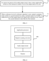
- an embodiment of this application provides a pop sound suppression terminal 400.
- the terminal 400 includes an application processor (AP), a digital-to-analog converter (DAC), an audio output circuit, and a headset.
- AP application processor
- DAC digital-to-analog converter
- audio output circuit an audio output circuit
- headset a headset
- FIG. 2 For a structure of the audio output circuit, refer to FIG. 2 .
- the application processor is configured to: obtain a digital audio bitstream, and output the digital audio bitstream to the digital-to-analog converter.
- the digital-to-analog converter is configured to: convert the digital audio bitstream into an analog audio signal, and output the analog audio signal to the audio output circuit.
- the audio output circuit is configured to: convert the analog audio signal into a driving analog audio signal having a driving capability, and output the driving analog audio signal to the headset.
- pop sounds can be greatly reduced in a common-mode establishment process of the audio output circuit in a single power supply and AC coupling mode, thereby improving user experience.
- All or some of the foregoing embodiments may be implemented by using software, hardware, or any combination thereof.
- the software is used to implement the embodiments, all or some of the embodiments may be implemented in a form of a computer program product.
- the computer program product includes one or more computer instructions.
- the computer may be a general-purpose computer, a special-purpose computer, a computer network, or another programmable apparatus.
- the computer instructions may be stored in a computer readable storage medium, or may be transmitted from a computer readable storage medium to another computer readable storage medium.
- the computer instructions may be transmitted from a website, computer, server, or data center to another website, computer, server, or data center in a wired (for example, a coaxial cable, a twisted pair, or an optical fiber) or wireless (for example, infrared, radio, or microwave) manner.
- the computer readable storage medium may be any usable medium accessible to the computer, or a data storage device, such as a server or a data center, integrating one or more usable media.
- the usable medium may be a magnetic medium (for example, a floppy disk, a hard disk, or a magnetic tape), an optical medium (for example, an optical disc), a semiconductor medium (for example, a solid-state drive), or the like.
Landscapes
- Engineering & Computer Science (AREA)
- Physics & Mathematics (AREA)
- Acoustics & Sound (AREA)
- Signal Processing (AREA)
- Power Engineering (AREA)
- Theoretical Computer Science (AREA)
- Health & Medical Sciences (AREA)
- General Health & Medical Sciences (AREA)
- Otolaryngology (AREA)
- Multimedia (AREA)
- Amplifiers (AREA)
Description
- This application relates to the circuit field, and in particular, to a pop sound suppression method, an audio output circuit, and a terminal.
- Human beings are extremely sensitive to a sudden signal change due to physiological particularity of human brains. Therefore, any non-ideal small change caused in a load path starting process may be sensed by human ears. Such a sound sounds like "pop" in most times and therefore is referred to as a pop sound.
- Existing audio data is classified into alternating current (AC) coupling output and direct current (DC) output based on output coupling types of the audio data.
FIG. 1 is a schematic diagram of an AC coupling output structure. A single power supply is used for AC coupling output. Therefore, when an input signal amplitude is zero, an output node (namely, an OUT node) is at a non-zero level and usually at a 1/2 power supply level, and therefore cannot directly drive a load. To ensure that there is no direct current on the load, an AC coupling capacitor needs to be connected between the OUT node and the load in series. When the AC coupling output structure (a single power supply structure) is used, because the OUT node and the load are separated by the AC coupling capacitor, before power-on, the OUT node is a weak driving node at a level approximate to 0. In a power-on process and in a period after the power-on is completed, by using an initial powered-on pop suppression circuit, the OUT node is pulled down to be at a zero level, to suppress a pop sound that may be generated during the power-on. However, during final working, the OUT node has a non-zero common-mode level (usually 1/2 VDD), and an actual signal of the OUT node is the non-zero common-mode level (DC level) plus an audio AC signal. - Therefore, it can be learned that, a level of the OUT node needs to gradually change from an initial zero level to a common-mode level that is a 1/2 power supply level, and a pop sound is very easily generated in such a change process. In view of this, this application provides a pop sound suppression solution, to suppress a pop sound generated when the AC coupling output structure is used.
- U.S. Patent Publication Number
US2011/007912A1 discloses an audio subsystem having a waveform generation circuit that generates a power-up signal for controlling an electric signal used to drive a speaker during a power-up period in which the power-up signal has a positive second derivative during a first sub-period of the power-up period and has a negative second derivative during a second sub-period of the power-up period. The first sub-period spans at least one-fourth of the power-up period, and the second sub-period spans at least one-fourth of the power-up period. - U.S. Patent Publication Number
US2005/195991A1 discloses a method and system are disclosed for controlling pop noises in a sound broadcasting system. After controllably connecting an output of a drive amplifier to a first predetermined low voltage level through a first switch, a first portion of an operation control data set is input to a digital-to-analog converter (DAC) circuit for driving an output thereof to a second predetermined low voltage level, and a second portion of the operation control data set is also input to the DAC circuit and further to the drive amplifier to bring the output of the drive amplifier to a common mode voltage level over a predetermined rise-up time period for controlling the pop noises. - U.S. Patent Publication Number
US2009/196435A1 discloses an audio system that reduces or eliminates click and pop noise during power up and power down operations. The audio system includes a first operational amplifier OPA1, a second operational amplifier OPA2, resistors, and a noise reduction circuit. The noise reduction circuit comprises a ramp generator, a first FET, a second FET, and a resistor Roff. The output of the first operational amplifier OPA1 is adapted to couple to a speaker via an AC coupling capacitor Cac. - Embodiments of this application provide a pop sound suppression method and an audio output circuit, in accordance with the appended independent claims 1 and 3, respectively, to suppress a pop sound easily generated when an audio output circuit is in an AC coupling structure. Preferred embodiments are set forth in the appended dependent claims.
-
-
FIG. 1 is a schematic diagram of an AC coupling output structure; -
FIG. 2 is a structural diagram of an audio output circuit in an alternating current coupling structure according to an embodiment of this application; -
FIG. 3 is a flowchart of a pop sound suppression method according to an embodiment of this application; and -
FIG. 4 is a structural diagram of a pop sound suppression terminal according to an embodiment of this application. - The following clearly and completely describes the technical solutions in the embodiments of this application with reference to the accompanying drawings in the embodiments of this application.
- It can be learned from
FIG. 1 that, when an audio output circuit is in an AC coupling structure, because an OUT node and a load are separated by an AC coupling capacitor, before power-on, the OUT node is a weak driving node at a level approximate to 0. However, during final working, the OUT node has a non-zero common-mode level, and an actual signal of the OUT node is the non-zero common-mode level plus an audio AC signal. - Therefore, it can be learned that, a level of the OUT node needs to gradually change from an initial zero level to a common-mode level, and a pop sound is very easily generated in such a change process.
- In view of the foregoing problem, the embodiments of this application provide a pop sound suppression method, an audio output circuit, and a terminal, to suppress a pop sound easily generated when an audio output circuit is in an AC coupling structure. The method and the apparatuses are based on a same invention concept. Because problem resolving principles of the method and the apparatuses are similar, mutual references may be made to implementation of the apparatuses and the method, and no repeated description is provided. In the embodiments of this application, in a power-on process of the audio output circuit, a reference level (VREF) generation circuit pin and an external capacitor in an existing audio circuit are used, no other pin and peripheral circuit are added, only one common-mode switch is added to an internal circuit, the original audio circuit is not modified, and no more constraints are imposed on the original audio circuit. Therefore, final costs are not increased.
-
FIG. 2 is a structural diagram of an audio output circuit in an alternating current coupling structure according to an embodiment of this application. The audio output circuit includes an output power amplifier (OUTPUT PA), a common-mode level buffer (vcm buffer), a reference level generation circuit including a reference level generation module and a reference level decoupling capacitor, a noise suppression module, the reference level generation module, a powered-on pop sound suppression switch, and a common-mode switch. The reference level generation circuit is coupled to the common-mode level buffer, the powered-on pop sound suppression switch is coupled to an output node of the output power amplifier and a local ground, and the common-mode switch is coupled to the output node and the common-mode level buffer. The powered-on pop sound suppression switch and the common-mode switch are components newly added to an existing audio output circuit that is used. - The powered-on pop sound suppression switch is configured to: in a power-on process of the audio output circuit, control a level of the output node to be zero.
- The common-mode switch is configured to: when a reference level of the reference level generation circuit is zero, control the level of the output node to be equal to the reference level.
- The noise suppression module is configured to enable the level of the output node to be zero in the power-on process of the audio output circuit.
- The reference level generation module is configured to control the reference level of the reference level generation circuit to rise from zero to a common-mode level, to enable the level of the output node to rise from zero to the common-mode level within preset duration.
- The audio output circuit further includes a first control circuit and a second control circuit.
- The first control circuit is configured to: in the power-on process of the audio output circuit, close the powered-on pop sound suppression switch at a first moment to enable the level of the output node to be zero.
- The second control circuit is configured to: when the reference level of the reference level generation circuit is zero, control the common-mode switch at a second moment by using the common-mode level buffer, to enable the level of the output node to be equal to the reference level, where the second moment is later than the first moment.
- The audio output circuit further includes a third control circuit, configured to: open the powered-on pop sound suppression switch at a third moment after the common-mode switch is controlled, when the reference level of the reference level generation circuit is zero, at the second moment to enable the level of the output node to be zero, where the third moment is later than the second moment;
- control the reference level of the reference level generation circuit to rise from zero to a common-mode level, to enable the level of the output node to rise from zero to the common-mode level within preset duration; and
- start the output power amplifier, and drive, by using the reference level generation circuit, the output node to be at the common-mode level within the preset duration.
- Optionally, the common-mode level is a half of a rated working level of the output power amplifier.
- In the audio output circuit, in the power-on process, by using the powered-on pop sound suppression switch, the output node is initially pulled down to be at a zero level; and then when the reference level generation module is not powered on and the reference level of the reference level generation circuit is zero, by using the common-mode switch, the output node is pulled down to be at a level that is the same as the reference level of the reference level generation circuit, namely, a zero level. Therefore, no pop sound is generated in the audio output circuit before power-on. In the power-on process, the reference level generation module starts to be powered on. The reference level rises very slowly due to the reference level generation circuit. Therefore, the common-mode level rises slowly, and the level of the output node rises slowly from the zero level to the common-mode level, generating only an infrasound wave without generating a pop sound. Then, the OUTPUT PA is started. If an offset (offset) of the OUTPUT PA is not considered, the output node is driven by the OUTPUT PA to be at the common-mode level. Compared with the previous operation of pulling, by using the VCM switch, the output node to be at the common-mode level, this solution does not change the level, and therefore no pop sound is generated.
- It should be noted that, for the operation of pulling, by using the common-mode switch, the output node down to be at the common-mode level and the operation of driving, by using the OUTPUT PA, the output node to be at the common-mode level, the level of the output node does not change. Therefore, even if the OUTPUT PA is enabled before the reference level is completely established, the output node does not jump, and therefore no pop sound is generated. Only such a design that the common-mode level buffer can still normally work when the reference level is equal to 0 is required. In addition, the OUTPUT PA of the audio output circuit does not need to be modified, the reference level generation circuit is used, the capacitor is required in the existing audio circuit for noise reduction, and no other pin and peripheral element are added, thereby reducing circuit costs.
- Based on the audio output circuit shown in
FIG. 2 , referring toFIG. 3 , an embodiment of this application provides a pop sound suppression method. A specific procedure is as follows: - Step 30: In a power-on process of the audio output circuit, close the powered-on pop sound suppression switch at a first moment to enable a level of the output node to be zero.
- Step 31: When a reference level of the reference level generation circuit is zero, control the common-mode switch at a second moment by using the common-mode level buffer, to enable the level of the output node to be equal to the reference level, where the second moment is later than the first moment.
- After the common-mode switch is controlled, when the reference level of the reference level generation circuit is zero, at the second moment to enable the level of the output node to be zero, the method further includes:
- opening the powered-on pop sound suppression switch at a third moment, where the third moment is later than the second moment;
- controlling the reference level of the reference level generation circuit to rise from zero to a common-mode level, to enable the level of the output node to rise from zero to the common-mode level within preset duration; and
- starting the output power amplifier, and driving, by using the reference level generation circuit, the output node to be at the common-mode level within the preset duration.
- Optionally, the common-mode level is a half of a rated working level of the output power amplifier.
- Referring to
FIG. 4 , an embodiment of this application provides a popsound suppression terminal 400. The terminal 400 includes an application processor (AP), a digital-to-analog converter (DAC), an audio output circuit, and a headset. For a structure of the audio output circuit, refer toFIG. 2 . - The application processor is configured to: obtain a digital audio bitstream, and output the digital audio bitstream to the digital-to-analog converter.
- The digital-to-analog converter is configured to: convert the digital audio bitstream into an analog audio signal, and output the analog audio signal to the audio output circuit.
- The audio output circuit is configured to: convert the analog audio signal into a driving analog audio signal having a driving capability, and output the driving analog audio signal to the headset.
- In conclusion, according to the noise suppression solution provided in the embodiments of this application, pop sounds can be greatly reduced in a common-mode establishment process of the audio output circuit in a single power supply and AC coupling mode, thereby improving user experience.
- All or some of the foregoing embodiments may be implemented by using software, hardware, or any combination thereof. When the software is used to implement the embodiments, all or some of the embodiments may be implemented in a form of a computer program product.
- The computer program product includes one or more computer instructions. When the computer program instructions are loaded and executed on a computer, all or some of the procedures or functions according to the embodiments of the present invention are generated. The computer may be a general-purpose computer, a special-purpose computer, a computer network, or another programmable apparatus. The computer instructions may be stored in a computer readable storage medium, or may be transmitted from a computer readable storage medium to another computer readable storage medium. For example, the computer instructions may be transmitted from a website, computer, server, or data center to another website, computer, server, or data center in a wired (for example, a coaxial cable, a twisted pair, or an optical fiber) or wireless (for example, infrared, radio, or microwave) manner. The computer readable storage medium may be any usable medium accessible to the computer, or a data storage device, such as a server or a data center, integrating one or more usable media. The usable medium may be a magnetic medium (for example, a floppy disk, a hard disk, or a magnetic tape), an optical medium (for example, an optical disc), a semiconductor medium (for example, a solid-state drive), or the like.
- Apparently, a person skilled in the art can make various modifications and variations to this application without departing from the scope of the claims of this application. In this way, this application is intended to cover these modifications and variations provided that they fall within the scope of the claims of this application.
Claims (5)
- A pop sound suppression method, applied to an audio output circuit in an alternating current
coupling structure, wherein the audio output circuit comprises an output power amplifier (OUTPUT PA), a common-mode voltage buffer, a reference voltage generation circuit, a powered-on pop sound suppression switch, and a common-mode switch, the reference voltage generation circuit is coupled to the common-mode voltage buffer, the powered-on pop sound suppression switch is coupled between an output node (OUT) of the output power amplifier and a local ground, and the common-mode switch is coupled between the output node of the output power amplifier and an output of the common-mode voltage buffer; and the method comprises:in a power-on process of the audio output circuit, closing (30) the powered-on pop sound suppression switch at a first moment to enable a voltage level of the output node to be zero; andwhen a reference voltage of the reference voltage generation circuit is zero, close the common-mode switch at a second moment, wherein the second moment is later than the first moment;wherein after the common-mode switch is closed, when the reference voltage of the reference voltage generation circuit is zero, at the second moment, to enable the voltage level of the output node to be zero, the method further comprises:opening the powered-on pop sound suppression switch at a third moment, wherein the third moment is later than the second moment;controlling the reference voltage of the reference voltage generation circuit to rise from zero to a common-mode voltage, to enable the voltage level of the output node to rise from zero to the common-mode voltage within preset duration; andstarting the output power amplifier, and driving, by using the reference voltage generation circuit, the output node to be at the common-mode voltage within the preset duration. - The method according to claim 1, wherein the common-mode voltage is a half of a power supply voltage of the output power amplifier.
- An audio output circuit in an alternating current coupling structure, comprising an output power amplifier (OUTPUT PA), a common-mode voltage buffer, a reference voltage generation circuit, a powered-on pop sound suppression switch, and a common-mode switch, wherein the reference voltage generation circuit is coupled to the common-mode voltage buffer, the powered-on pop sound suppression switch is coupled between an output node (OUT) of the output power amplifier and a local ground, and the common-mode switch is coupled between the output node of the output power amplifier and an output of the common-mode voltage buffer;the audio output circuit further comprises: a first control circuit and a second control circuit, whereinthe first control circuit is configured to: in power-on process of the audio output circuit, close the powered-on pop sound suppression switch at a first moment to enable a voltage level of the output node to be zero;the second control circuit is configured to: when a reference voltage of the reference voltage generation circuit is zero, close the common-mode switch at a second moment, wherein the second moment is later than the first moment; andthe audio output circuit further comprises a third control circuit, configured to: open the powered-on pop sound suppression switch at a third moment after the common-mode switch is closed, when the reference voltage of the reference voltage generation circuit is zero, wherein the third moment is later than the second moment;control the reference voltage of the reference voltage generation circuit to rise from zero to a common-mode voltage, to enable the voltage level of the output node to rise from zero to the common-mode voltage within preset duration; andstart the output power amplifier, and drive, by using the reference voltage generation circuit, the output node to be at the common-mode voltage within the preset duration.
- The audio output circuit according to claim 3, wherein the common-mode voltage is a half of power supply voltage of the output power amplifier.
- A terminal (400), comprising an application processor, a digital-to-analog converter, the audio output circuit according to claim 3 or 4, and a headset, whereinthe application processor is configured to: obtain a digital audio bitstream, and output the digital audio bitstream to the digital-to-analog converter;the digital-to-analog converter is configured to: convert the digital audio bitstream into an analog audio signal, and output the analog audio signal to the audio output circuit; andthe audio output circuit is configured to: convert the analog audio signal into a driving analog audio signal having a driving capability, and output the driving analog audio signal to the headset.
Applications Claiming Priority (2)
| Application Number | Priority Date | Filing Date | Title |
|---|---|---|---|
| CN201710296857.6A CN108810735B (en) | 2017-04-28 | 2017-04-28 | POP sound suppression method, audio output circuit and terminal |
| PCT/CN2018/079586 WO2018196507A1 (en) | 2017-04-28 | 2018-03-20 | Method for suppressing pop sound, audio output circuit, and terminal |
Publications (3)
| Publication Number | Publication Date |
|---|---|
| EP3579576A1 EP3579576A1 (en) | 2019-12-11 |
| EP3579576A4 EP3579576A4 (en) | 2020-03-04 |
| EP3579576B1 true EP3579576B1 (en) | 2023-08-30 |
Family
ID=63919404
Family Applications (1)
| Application Number | Title | Priority Date | Filing Date |
|---|---|---|---|
| EP18790297.8A Active EP3579576B1 (en) | 2017-04-28 | 2018-03-20 | Method for suppressing pop sound, audio output circuit, and terminal |
Country Status (4)
| Country | Link |
|---|---|
| US (1) | US10893360B2 (en) |
| EP (1) | EP3579576B1 (en) |
| CN (2) | CN108810735B (en) |
| WO (1) | WO2018196507A1 (en) |
Families Citing this family (5)
| Publication number | Priority date | Publication date | Assignee | Title |
|---|---|---|---|---|
| TWI722279B (en) * | 2018-04-09 | 2021-03-21 | 瑞昱半導體股份有限公司 | Audio codec circuit capable of avoiding pop-noise |
| GB2591523B (en) * | 2020-01-31 | 2022-03-23 | Cirrus Logic Int Semiconductor Ltd | Audio amplifier circuitry |
| CN111510826B (en) * | 2020-05-21 | 2024-05-31 | 杭州国芯科技股份有限公司 | Circuit and method for eliminating shutdown pop sound of media playing device |
| CN114527952A (en) * | 2021-12-30 | 2022-05-24 | 广东思派康电子科技有限公司 | Method and device for eliminating POP sound caused by audio switching |
| CN114630230B (en) | 2022-05-12 | 2022-10-14 | 荣耀终端有限公司 | Electronic equipment, pull-up circuit and method for suppressing earphone POP sound |
Citations (1)
| Publication number | Priority date | Publication date | Assignee | Title |
|---|---|---|---|---|
| US20090196435A1 (en) * | 2008-01-31 | 2009-08-06 | Qualcomm Incorporated | System and method of reducing click and pop noise in audio playback devices |
Family Cites Families (22)
| Publication number | Priority date | Publication date | Assignee | Title |
|---|---|---|---|---|
| JP2585249B2 (en) | 1987-03-06 | 1997-02-26 | 株式会社東芝 | Shock noise prevention circuit for audio amplifier. |
| US7092534B2 (en) * | 2004-03-02 | 2006-08-15 | Via Telecom Co., Ltd. | Method and system for reducing pop noise of a sound broadcasting instrument |
| EP1689075B1 (en) | 2005-02-03 | 2018-07-11 | Texas Instruments Inc. | Multi-stage amplifier to reduce pop noise |
| EP1689076B1 (en) | 2005-02-03 | 2019-08-07 | Texas Instruments Inc. | Track and hold circuit to reduce pop noise |
| CN101106368A (en) * | 2006-07-12 | 2008-01-16 | 华硕电脑股份有限公司 | Anti-explosion sound circuit |
| KR100810853B1 (en) | 2006-08-25 | 2008-03-06 | 삼성전자주식회사 | Apparatus and method for preventing pop noise in an audio output device |
| TW200836576A (en) * | 2007-02-27 | 2008-09-01 | Generalplus Technology Inc | Circuit for eliminating blast noise during power-on and power-off using smoothly changed waveform |
| CN101309071B (en) * | 2007-05-18 | 2010-06-23 | 展讯通信(上海)有限公司 | A device for suppressing transient noise of audio power amplifier |
| TW200937994A (en) * | 2008-02-19 | 2009-09-01 | Sunplus Mmedia Inc | Sound driving circuit for reducing pop noise during powering on and off |
| CN101350593B (en) * | 2008-08-26 | 2010-12-08 | 四川和芯微电子股份有限公司 | Circuit for suppressing POP noise |
| TWI403181B (en) * | 2009-06-23 | 2013-07-21 | Richtek Technology Corp | Power off delay circuit and method, and audio system with power off delay |
| US20110007912A1 (en) * | 2009-07-07 | 2011-01-13 | Mediatek Singapore Pte. Ltd. | Double integral method of powering up or down a speaker |
| CN102572629A (en) * | 2010-12-10 | 2012-07-11 | 炬力集成电路设计有限公司 | Circuit for suppressing POP sound in earphone, and earphone |
| US8447046B2 (en) * | 2011-01-13 | 2013-05-21 | Issc Technologies Corp. | Circuit with three-stage of power-on sequence used for suppressing the pop noise in audio system |
| CN102421051A (en) * | 2011-12-16 | 2012-04-18 | 四川和芯微电子股份有限公司 | Pop noise suppression circuit and system |
| CN103248985B (en) * | 2012-02-03 | 2015-12-09 | 安凯(广州)微电子技术有限公司 | A kind of audio frequency power amplifier squelch-circuit with the straight electric capacity of isolation |
| CN102629855B (en) * | 2012-04-13 | 2015-04-08 | 成都芯源系统有限公司 | Noise suppression circuit and control method thereof |
| CN102946578B (en) * | 2012-11-26 | 2016-03-02 | 成都锐成芯微科技有限责任公司 | A kind of audio earphone amplifier of exempting from switch P OP sound |
| CN103402157B (en) * | 2013-08-02 | 2016-09-28 | 昆腾微电子股份有限公司 | Voicefrequency circuit, audio system and the method eliminating POP noise |
| CN104883641A (en) * | 2014-02-28 | 2015-09-02 | 维沃移动通信有限公司 | Mobile terminal of realizing high fidelity music play |
| FR3025373B1 (en) * | 2014-08-26 | 2018-06-08 | Dolphin Integration Sa | REDUCTION NOISE REDUCTION CIRCUIT |
| CN105554634B (en) * | 2015-12-31 | 2018-09-28 | 苏州芯动科技有限公司 | A kind of audio output POP sound elimination circuit |
-
2017
- 2017-04-28 CN CN201710296857.6A patent/CN108810735B/en active Active
- 2017-04-28 CN CN202010154963.2A patent/CN111464917B/en active Active
-
2018
- 2018-03-20 EP EP18790297.8A patent/EP3579576B1/en active Active
- 2018-03-20 WO PCT/CN2018/079586 patent/WO2018196507A1/en not_active Ceased
-
2019
- 2019-10-14 US US16/601,133 patent/US10893360B2/en active Active
Patent Citations (1)
| Publication number | Priority date | Publication date | Assignee | Title |
|---|---|---|---|---|
| US20090196435A1 (en) * | 2008-01-31 | 2009-08-06 | Qualcomm Incorporated | System and method of reducing click and pop noise in audio playback devices |
Also Published As
| Publication number | Publication date |
|---|---|
| EP3579576A1 (en) | 2019-12-11 |
| US20200045417A1 (en) | 2020-02-06 |
| WO2018196507A1 (en) | 2018-11-01 |
| CN111464917A (en) | 2020-07-28 |
| CN108810735A (en) | 2018-11-13 |
| CN111464917B (en) | 2022-04-22 |
| EP3579576A4 (en) | 2020-03-04 |
| CN108810735B (en) | 2020-03-20 |
| US10893360B2 (en) | 2021-01-12 |
Similar Documents
| Publication | Publication Date | Title |
|---|---|---|
| US10893360B2 (en) | Pop sound suppression method, audio output circuit, and terminal | |
| GB2544822B (en) | Systems and methods for preventing distortion due to supply-based changes in an audio playback system | |
| US10397700B2 (en) | System and method for loudspeaker protection | |
| CN1977478B (en) | Method and system for reducing instantaneous noise of a sound broadcasting instrument | |
| CN101010873A (en) | Audio signal amplifying circuit and electronic device using the same | |
| US20200228069A1 (en) | Audio play circuit and audio play device | |
| US8325940B2 (en) | Power management controller for drivers | |
| CN106231491B (en) | It is a kind of to eliminate the method for extracting power down POP sound | |
| TWI352475B (en) | Device and method for surge prevention | |
| KR101625768B1 (en) | Amplifier with improved noise reduction | |
| JP4490985B2 (en) | Method and apparatus for controlling fan motor | |
| JP4787742B2 (en) | SIGNAL OUTPUT CIRCUIT, AUDIO SIGNAL OUTPUT DEVICE USING THE SAME, ELECTRONIC DEVICE | |
| US7558158B2 (en) | Electronic apparatus and method for implementing an intelligent wake mode | |
| CN105580269B (en) | Amplifier with Improved Noise Reduction | |
| WO2018157503A1 (en) | Volume adjustment method and device for earphones, and earphones | |
| KR20140006668A (en) | Hearing aid and hearing measurement and correction method using it | |
| TW201044772A (en) | Circuits and methods for reducing pop noise in class D amplifiers | |
| WO2023093684A1 (en) | Audio system for eliminating turn-on pop noise and power supply control method | |
| JP5018795B2 (en) | Voltage supply circuit and circuit device | |
| JP2013093800A (en) | Output circuit of audio apparatus and control method thereof, and electronic apparatus including the same | |
| JP2008158795A (en) | Voltage supply circuit and circuit device | |
| US20260032383A1 (en) | Audio playing module and audio processing circuit thereof, and electronic device | |
| JP2007116532A (en) | Audio muting circuit and method | |
| CN115186126A (en) | Magnetic field generating method and related equipment | |
| CN114567265A (en) | Noise suppression circuit, method and electronic equipment |
Legal Events
| Date | Code | Title | Description |
|---|---|---|---|
| STAA | Information on the status of an ep patent application or granted ep patent |
Free format text: STATUS: THE INTERNATIONAL PUBLICATION HAS BEEN MADE |
|
| PUAI | Public reference made under article 153(3) epc to a published international application that has entered the european phase |
Free format text: ORIGINAL CODE: 0009012 |
|
| STAA | Information on the status of an ep patent application or granted ep patent |
Free format text: STATUS: REQUEST FOR EXAMINATION WAS MADE |
|
| 17P | Request for examination filed |
Effective date: 20190906 |
|
| AK | Designated contracting states |
Kind code of ref document: A1 Designated state(s): AL AT BE BG CH CY CZ DE DK EE ES FI FR GB GR HR HU IE IS IT LI LT LU LV MC MK MT NL NO PL PT RO RS SE SI SK SM TR |
|
| AX | Request for extension of the european patent |
Extension state: BA ME |
|
| A4 | Supplementary search report drawn up and despatched |
Effective date: 20200203 |
|
| RIC1 | Information provided on ipc code assigned before grant |
Ipc: H03F 1/30 20060101ALI20200128BHEP Ipc: H03G 3/30 20060101ALI20200128BHEP Ipc: H04R 3/00 20060101AFI20200128BHEP |
|
| DAV | Request for validation of the european patent (deleted) | ||
| DAX | Request for extension of the european patent (deleted) | ||
| STAA | Information on the status of an ep patent application or granted ep patent |
Free format text: STATUS: EXAMINATION IS IN PROGRESS |
|
| 17Q | First examination report despatched |
Effective date: 20211019 |
|
| REG | Reference to a national code |
Ref country code: DE Ref legal event code: R079 Free format text: PREVIOUS MAIN CLASS: H04R0003000000 Ipc: H03F0003181000 Ref document number: 602018056513 Country of ref document: DE |
|
| GRAP | Despatch of communication of intention to grant a patent |
Free format text: ORIGINAL CODE: EPIDOSNIGR1 |
|
| STAA | Information on the status of an ep patent application or granted ep patent |
Free format text: STATUS: GRANT OF PATENT IS INTENDED |
|
| RIC1 | Information provided on ipc code assigned before grant |
Ipc: H04R 3/00 20060101ALI20230329BHEP Ipc: H03F 1/30 20060101ALI20230329BHEP Ipc: H03G 3/34 20060101ALI20230329BHEP Ipc: H03F 3/181 20060101AFI20230329BHEP |
|
| INTG | Intention to grant announced |
Effective date: 20230425 |
|
| GRAS | Grant fee paid |
Free format text: ORIGINAL CODE: EPIDOSNIGR3 |
|
| GRAA | (expected) grant |
Free format text: ORIGINAL CODE: 0009210 |
|
| STAA | Information on the status of an ep patent application or granted ep patent |
Free format text: STATUS: THE PATENT HAS BEEN GRANTED |
|
| AK | Designated contracting states |
Kind code of ref document: B1 Designated state(s): AL AT BE BG CH CY CZ DE DK EE ES FI FR GB GR HR HU IE IS IT LI LT LU LV MC MK MT NL NO PL PT RO RS SE SI SK SM TR |
|
| REG | Reference to a national code |
Ref country code: GB Ref legal event code: FG4D |
|
| REG | Reference to a national code |
Ref country code: CH Ref legal event code: EP |
|
| REG | Reference to a national code |
Ref country code: DE Ref legal event code: R096 Ref document number: 602018056513 Country of ref document: DE |
|
| REG | Reference to a national code |
Ref country code: IE Ref legal event code: FG4D |
|
| REG | Reference to a national code |
Ref country code: LT Ref legal event code: MG9D |
|
| REG | Reference to a national code |
Ref country code: NL Ref legal event code: MP Effective date: 20230830 |
|
| REG | Reference to a national code |
Ref country code: AT Ref legal event code: MK05 Ref document number: 1606722 Country of ref document: AT Kind code of ref document: T Effective date: 20230830 |
|
| PG25 | Lapsed in a contracting state [announced via postgrant information from national office to epo] |
Ref country code: GR Free format text: LAPSE BECAUSE OF FAILURE TO SUBMIT A TRANSLATION OF THE DESCRIPTION OR TO PAY THE FEE WITHIN THE PRESCRIBED TIME-LIMIT Effective date: 20231201 |
|
| PG25 | Lapsed in a contracting state [announced via postgrant information from national office to epo] |
Ref country code: IS Free format text: LAPSE BECAUSE OF FAILURE TO SUBMIT A TRANSLATION OF THE DESCRIPTION OR TO PAY THE FEE WITHIN THE PRESCRIBED TIME-LIMIT Effective date: 20231230 |
|
| PG25 | Lapsed in a contracting state [announced via postgrant information from national office to epo] |
Ref country code: SE Free format text: LAPSE BECAUSE OF FAILURE TO SUBMIT A TRANSLATION OF THE DESCRIPTION OR TO PAY THE FEE WITHIN THE PRESCRIBED TIME-LIMIT Effective date: 20230830 Ref country code: RS Free format text: LAPSE BECAUSE OF FAILURE TO SUBMIT A TRANSLATION OF THE DESCRIPTION OR TO PAY THE FEE WITHIN THE PRESCRIBED TIME-LIMIT Effective date: 20230830 Ref country code: NO Free format text: LAPSE BECAUSE OF FAILURE TO SUBMIT A TRANSLATION OF THE DESCRIPTION OR TO PAY THE FEE WITHIN THE PRESCRIBED TIME-LIMIT Effective date: 20231130 Ref country code: LV Free format text: LAPSE BECAUSE OF FAILURE TO SUBMIT A TRANSLATION OF THE DESCRIPTION OR TO PAY THE FEE WITHIN THE PRESCRIBED TIME-LIMIT Effective date: 20230830 Ref country code: LT Free format text: LAPSE BECAUSE OF FAILURE TO SUBMIT A TRANSLATION OF THE DESCRIPTION OR TO PAY THE FEE WITHIN THE PRESCRIBED TIME-LIMIT Effective date: 20230830 Ref country code: IS Free format text: LAPSE BECAUSE OF FAILURE TO SUBMIT A TRANSLATION OF THE DESCRIPTION OR TO PAY THE FEE WITHIN THE PRESCRIBED TIME-LIMIT Effective date: 20231230 Ref country code: HR Free format text: LAPSE BECAUSE OF FAILURE TO SUBMIT A TRANSLATION OF THE DESCRIPTION OR TO PAY THE FEE WITHIN THE PRESCRIBED TIME-LIMIT Effective date: 20230830 Ref country code: GR Free format text: LAPSE BECAUSE OF FAILURE TO SUBMIT A TRANSLATION OF THE DESCRIPTION OR TO PAY THE FEE WITHIN THE PRESCRIBED TIME-LIMIT Effective date: 20231201 Ref country code: FI Free format text: LAPSE BECAUSE OF FAILURE TO SUBMIT A TRANSLATION OF THE DESCRIPTION OR TO PAY THE FEE WITHIN THE PRESCRIBED TIME-LIMIT Effective date: 20230830 Ref country code: AT Free format text: LAPSE BECAUSE OF FAILURE TO SUBMIT A TRANSLATION OF THE DESCRIPTION OR TO PAY THE FEE WITHIN THE PRESCRIBED TIME-LIMIT Effective date: 20230830 |
|
| PG25 | Lapsed in a contracting state [announced via postgrant information from national office to epo] |
Ref country code: PL Free format text: LAPSE BECAUSE OF FAILURE TO SUBMIT A TRANSLATION OF THE DESCRIPTION OR TO PAY THE FEE WITHIN THE PRESCRIBED TIME-LIMIT Effective date: 20230830 Ref country code: NL Free format text: LAPSE BECAUSE OF FAILURE TO SUBMIT A TRANSLATION OF THE DESCRIPTION OR TO PAY THE FEE WITHIN THE PRESCRIBED TIME-LIMIT Effective date: 20230830 |
|
| PG25 | Lapsed in a contracting state [announced via postgrant information from national office to epo] |
Ref country code: ES Free format text: LAPSE BECAUSE OF FAILURE TO SUBMIT A TRANSLATION OF THE DESCRIPTION OR TO PAY THE FEE WITHIN THE PRESCRIBED TIME-LIMIT Effective date: 20230830 |
|
| PG25 | Lapsed in a contracting state [announced via postgrant information from national office to epo] |
Ref country code: SM Free format text: LAPSE BECAUSE OF FAILURE TO SUBMIT A TRANSLATION OF THE DESCRIPTION OR TO PAY THE FEE WITHIN THE PRESCRIBED TIME-LIMIT Effective date: 20230830 Ref country code: RO Free format text: LAPSE BECAUSE OF FAILURE TO SUBMIT A TRANSLATION OF THE DESCRIPTION OR TO PAY THE FEE WITHIN THE PRESCRIBED TIME-LIMIT Effective date: 20230830 Ref country code: ES Free format text: LAPSE BECAUSE OF FAILURE TO SUBMIT A TRANSLATION OF THE DESCRIPTION OR TO PAY THE FEE WITHIN THE PRESCRIBED TIME-LIMIT Effective date: 20230830 Ref country code: EE Free format text: LAPSE BECAUSE OF FAILURE TO SUBMIT A TRANSLATION OF THE DESCRIPTION OR TO PAY THE FEE WITHIN THE PRESCRIBED TIME-LIMIT Effective date: 20230830 Ref country code: DK Free format text: LAPSE BECAUSE OF FAILURE TO SUBMIT A TRANSLATION OF THE DESCRIPTION OR TO PAY THE FEE WITHIN THE PRESCRIBED TIME-LIMIT Effective date: 20230830 Ref country code: CZ Free format text: LAPSE BECAUSE OF FAILURE TO SUBMIT A TRANSLATION OF THE DESCRIPTION OR TO PAY THE FEE WITHIN THE PRESCRIBED TIME-LIMIT Effective date: 20230830 Ref country code: PT Free format text: LAPSE BECAUSE OF FAILURE TO SUBMIT A TRANSLATION OF THE DESCRIPTION OR TO PAY THE FEE WITHIN THE PRESCRIBED TIME-LIMIT Effective date: 20240102 Ref country code: SK Free format text: LAPSE BECAUSE OF FAILURE TO SUBMIT A TRANSLATION OF THE DESCRIPTION OR TO PAY THE FEE WITHIN THE PRESCRIBED TIME-LIMIT Effective date: 20230830 |
|
| REG | Reference to a national code |
Ref country code: DE Ref legal event code: R097 Ref document number: 602018056513 Country of ref document: DE |
|
| PLBE | No opposition filed within time limit |
Free format text: ORIGINAL CODE: 0009261 |
|
| STAA | Information on the status of an ep patent application or granted ep patent |
Free format text: STATUS: NO OPPOSITION FILED WITHIN TIME LIMIT |
|
| PG25 | Lapsed in a contracting state [announced via postgrant information from national office to epo] |
Ref country code: SI Free format text: LAPSE BECAUSE OF FAILURE TO SUBMIT A TRANSLATION OF THE DESCRIPTION OR TO PAY THE FEE WITHIN THE PRESCRIBED TIME-LIMIT Effective date: 20230830 |
|
| 26N | No opposition filed |
Effective date: 20240603 |
|
| REG | Reference to a national code |
Ref country code: CH Ref legal event code: PL |
|
| PG25 | Lapsed in a contracting state [announced via postgrant information from national office to epo] |
Ref country code: BG Free format text: LAPSE BECAUSE OF FAILURE TO SUBMIT A TRANSLATION OF THE DESCRIPTION OR TO PAY THE FEE WITHIN THE PRESCRIBED TIME-LIMIT Effective date: 20230830 |
|
| PG25 | Lapsed in a contracting state [announced via postgrant information from national office to epo] |
Ref country code: LU Free format text: LAPSE BECAUSE OF NON-PAYMENT OF DUE FEES Effective date: 20240320 |
|
| PG25 | Lapsed in a contracting state [announced via postgrant information from national office to epo] |
Ref country code: MC Free format text: LAPSE BECAUSE OF FAILURE TO SUBMIT A TRANSLATION OF THE DESCRIPTION OR TO PAY THE FEE WITHIN THE PRESCRIBED TIME-LIMIT Effective date: 20230830 |
|
| GBPC | Gb: european patent ceased through non-payment of renewal fee |
Effective date: 20240320 |
|
| PG25 | Lapsed in a contracting state [announced via postgrant information from national office to epo] |
Ref country code: MC Free format text: LAPSE BECAUSE OF FAILURE TO SUBMIT A TRANSLATION OF THE DESCRIPTION OR TO PAY THE FEE WITHIN THE PRESCRIBED TIME-LIMIT Effective date: 20230830 Ref country code: LU Free format text: LAPSE BECAUSE OF NON-PAYMENT OF DUE FEES Effective date: 20240320 Ref country code: BG Free format text: LAPSE BECAUSE OF FAILURE TO SUBMIT A TRANSLATION OF THE DESCRIPTION OR TO PAY THE FEE WITHIN THE PRESCRIBED TIME-LIMIT Effective date: 20230830 |
|
| REG | Reference to a national code |
Ref country code: BE Ref legal event code: MM Effective date: 20240331 |
|
| PG25 | Lapsed in a contracting state [announced via postgrant information from national office to epo] |
Ref country code: BE Free format text: LAPSE BECAUSE OF NON-PAYMENT OF DUE FEES Effective date: 20240331 |
|
| PG25 | Lapsed in a contracting state [announced via postgrant information from national office to epo] |
Ref country code: GB Free format text: LAPSE BECAUSE OF NON-PAYMENT OF DUE FEES Effective date: 20240320 |
|
| PG25 | Lapsed in a contracting state [announced via postgrant information from national office to epo] |
Ref country code: IE Free format text: LAPSE BECAUSE OF NON-PAYMENT OF DUE FEES Effective date: 20240320 |
|
| PG25 | Lapsed in a contracting state [announced via postgrant information from national office to epo] |
Ref country code: IE Free format text: LAPSE BECAUSE OF NON-PAYMENT OF DUE FEES Effective date: 20240320 Ref country code: GB Free format text: LAPSE BECAUSE OF NON-PAYMENT OF DUE FEES Effective date: 20240320 Ref country code: BE Free format text: LAPSE BECAUSE OF NON-PAYMENT OF DUE FEES Effective date: 20240331 Ref country code: CH Free format text: LAPSE BECAUSE OF NON-PAYMENT OF DUE FEES Effective date: 20240331 |
|
| PG25 | Lapsed in a contracting state [announced via postgrant information from national office to epo] |
Ref country code: CY Free format text: LAPSE BECAUSE OF FAILURE TO SUBMIT A TRANSLATION OF THE DESCRIPTION OR TO PAY THE FEE WITHIN THE PRESCRIBED TIME-LIMIT; INVALID AB INITIO Effective date: 20180320 |
|
| PG25 | Lapsed in a contracting state [announced via postgrant information from national office to epo] |
Ref country code: HU Free format text: LAPSE BECAUSE OF FAILURE TO SUBMIT A TRANSLATION OF THE DESCRIPTION OR TO PAY THE FEE WITHIN THE PRESCRIBED TIME-LIMIT; INVALID AB INITIO Effective date: 20180320 |
|
| PG25 | Lapsed in a contracting state [announced via postgrant information from national office to epo] |
Ref country code: TR Free format text: LAPSE BECAUSE OF FAILURE TO SUBMIT A TRANSLATION OF THE DESCRIPTION OR TO PAY THE FEE WITHIN THE PRESCRIBED TIME-LIMIT Effective date: 20230830 |
|
| PGFP | Annual fee paid to national office [announced via postgrant information from national office to epo] |
Ref country code: DE Payment date: 20260204 Year of fee payment: 9 |
|
| PGFP | Annual fee paid to national office [announced via postgrant information from national office to epo] |
Ref country code: IT Payment date: 20260220 Year of fee payment: 9 |
|
| PGFP | Annual fee paid to national office [announced via postgrant information from national office to epo] |
Ref country code: FR Payment date: 20260209 Year of fee payment: 9 |