EP3579407A1 - Differential voltage-controlled (vco) oscillator - Google Patents
Differential voltage-controlled (vco) oscillator Download PDFInfo
- Publication number
- EP3579407A1 EP3579407A1 EP18305691.0A EP18305691A EP3579407A1 EP 3579407 A1 EP3579407 A1 EP 3579407A1 EP 18305691 A EP18305691 A EP 18305691A EP 3579407 A1 EP3579407 A1 EP 3579407A1
- Authority
- EP
- European Patent Office
- Prior art keywords
- transistors
- circuit according
- coupled
- varactors
- terminal
- Prior art date
- Legal status (The legal status is an assumption and is not a legal conclusion. Google has not performed a legal analysis and makes no representation as to the accuracy of the status listed.)
- Withdrawn
Links
Images

Classifications
-
- H—ELECTRICITY
- H03—ELECTRONIC CIRCUITRY
- H03B—GENERATION OF OSCILLATIONS, DIRECTLY OR BY FREQUENCY-CHANGING, BY CIRCUITS EMPLOYING ACTIVE ELEMENTS WHICH OPERATE IN A NON-SWITCHING MANNER; GENERATION OF NOISE BY SUCH CIRCUITS
- H03B5/00—Generation of oscillations using amplifier with regenerative feedback from output to input
- H03B5/08—Generation of oscillations using amplifier with regenerative feedback from output to input with frequency-determining element comprising lumped inductance and capacitance
- H03B5/12—Generation of oscillations using amplifier with regenerative feedback from output to input with frequency-determining element comprising lumped inductance and capacitance active element in amplifier being semiconductor device
- H03B5/1237—Generation of oscillations using amplifier with regenerative feedback from output to input with frequency-determining element comprising lumped inductance and capacitance active element in amplifier being semiconductor device comprising means for varying the frequency of the generator
- H03B5/124—Generation of oscillations using amplifier with regenerative feedback from output to input with frequency-determining element comprising lumped inductance and capacitance active element in amplifier being semiconductor device comprising means for varying the frequency of the generator the means comprising a voltage dependent capacitance
-
- H—ELECTRICITY
- H03—ELECTRONIC CIRCUITRY
- H03B—GENERATION OF OSCILLATIONS, DIRECTLY OR BY FREQUENCY-CHANGING, BY CIRCUITS EMPLOYING ACTIVE ELEMENTS WHICH OPERATE IN A NON-SWITCHING MANNER; GENERATION OF NOISE BY SUCH CIRCUITS
- H03B5/00—Generation of oscillations using amplifier with regenerative feedback from output to input
- H03B5/08—Generation of oscillations using amplifier with regenerative feedback from output to input with frequency-determining element comprising lumped inductance and capacitance
- H03B5/12—Generation of oscillations using amplifier with regenerative feedback from output to input with frequency-determining element comprising lumped inductance and capacitance active element in amplifier being semiconductor device
- H03B5/1206—Generation of oscillations using amplifier with regenerative feedback from output to input with frequency-determining element comprising lumped inductance and capacitance active element in amplifier being semiconductor device using multiple transistors for amplification
- H03B5/1218—Generation of oscillations using amplifier with regenerative feedback from output to input with frequency-determining element comprising lumped inductance and capacitance active element in amplifier being semiconductor device using multiple transistors for amplification the generator being of the balanced type
-
- H—ELECTRICITY
- H03—ELECTRONIC CIRCUITRY
- H03B—GENERATION OF OSCILLATIONS, DIRECTLY OR BY FREQUENCY-CHANGING, BY CIRCUITS EMPLOYING ACTIVE ELEMENTS WHICH OPERATE IN A NON-SWITCHING MANNER; GENERATION OF NOISE BY SUCH CIRCUITS
- H03B5/00—Generation of oscillations using amplifier with regenerative feedback from output to input
- H03B5/08—Generation of oscillations using amplifier with regenerative feedback from output to input with frequency-determining element comprising lumped inductance and capacitance
- H03B5/12—Generation of oscillations using amplifier with regenerative feedback from output to input with frequency-determining element comprising lumped inductance and capacitance active element in amplifier being semiconductor device
- H03B5/1206—Generation of oscillations using amplifier with regenerative feedback from output to input with frequency-determining element comprising lumped inductance and capacitance active element in amplifier being semiconductor device using multiple transistors for amplification
- H03B5/1212—Generation of oscillations using amplifier with regenerative feedback from output to input with frequency-determining element comprising lumped inductance and capacitance active element in amplifier being semiconductor device using multiple transistors for amplification the amplifier comprising a pair of transistors, wherein an output terminal of each being connected to an input terminal of the other, e.g. a cross coupled pair
-
- H—ELECTRICITY
- H03—ELECTRONIC CIRCUITRY
- H03B—GENERATION OF OSCILLATIONS, DIRECTLY OR BY FREQUENCY-CHANGING, BY CIRCUITS EMPLOYING ACTIVE ELEMENTS WHICH OPERATE IN A NON-SWITCHING MANNER; GENERATION OF NOISE BY SUCH CIRCUITS
- H03B5/00—Generation of oscillations using amplifier with regenerative feedback from output to input
- H03B5/08—Generation of oscillations using amplifier with regenerative feedback from output to input with frequency-determining element comprising lumped inductance and capacitance
- H03B5/12—Generation of oscillations using amplifier with regenerative feedback from output to input with frequency-determining element comprising lumped inductance and capacitance active element in amplifier being semiconductor device
- H03B5/1206—Generation of oscillations using amplifier with regenerative feedback from output to input with frequency-determining element comprising lumped inductance and capacitance active element in amplifier being semiconductor device using multiple transistors for amplification
- H03B5/1212—Generation of oscillations using amplifier with regenerative feedback from output to input with frequency-determining element comprising lumped inductance and capacitance active element in amplifier being semiconductor device using multiple transistors for amplification the amplifier comprising a pair of transistors, wherein an output terminal of each being connected to an input terminal of the other, e.g. a cross coupled pair
- H03B5/1215—Generation of oscillations using amplifier with regenerative feedback from output to input with frequency-determining element comprising lumped inductance and capacitance active element in amplifier being semiconductor device using multiple transistors for amplification the amplifier comprising a pair of transistors, wherein an output terminal of each being connected to an input terminal of the other, e.g. a cross coupled pair the current source or degeneration circuit being in common to both transistors of the pair, e.g. a cross-coupled long-tailed pair
-
- H—ELECTRICITY
- H03—ELECTRONIC CIRCUITRY
- H03B—GENERATION OF OSCILLATIONS, DIRECTLY OR BY FREQUENCY-CHANGING, BY CIRCUITS EMPLOYING ACTIVE ELEMENTS WHICH OPERATE IN A NON-SWITCHING MANNER; GENERATION OF NOISE BY SUCH CIRCUITS
- H03B5/00—Generation of oscillations using amplifier with regenerative feedback from output to input
- H03B5/08—Generation of oscillations using amplifier with regenerative feedback from output to input with frequency-determining element comprising lumped inductance and capacitance
- H03B5/12—Generation of oscillations using amplifier with regenerative feedback from output to input with frequency-determining element comprising lumped inductance and capacitance active element in amplifier being semiconductor device
- H03B5/1228—Generation of oscillations using amplifier with regenerative feedback from output to input with frequency-determining element comprising lumped inductance and capacitance active element in amplifier being semiconductor device the amplifier comprising one or more field effect transistors
-
- H—ELECTRICITY
- H03—ELECTRONIC CIRCUITRY
- H03B—GENERATION OF OSCILLATIONS, DIRECTLY OR BY FREQUENCY-CHANGING, BY CIRCUITS EMPLOYING ACTIVE ELEMENTS WHICH OPERATE IN A NON-SWITCHING MANNER; GENERATION OF NOISE BY SUCH CIRCUITS
- H03B5/00—Generation of oscillations using amplifier with regenerative feedback from output to input
- H03B5/08—Generation of oscillations using amplifier with regenerative feedback from output to input with frequency-determining element comprising lumped inductance and capacitance
- H03B5/12—Generation of oscillations using amplifier with regenerative feedback from output to input with frequency-determining element comprising lumped inductance and capacitance active element in amplifier being semiconductor device
- H03B5/1231—Generation of oscillations using amplifier with regenerative feedback from output to input with frequency-determining element comprising lumped inductance and capacitance active element in amplifier being semiconductor device the amplifier comprising one or more bipolar transistors
-
- H—ELECTRICITY
- H03—ELECTRONIC CIRCUITRY
- H03B—GENERATION OF OSCILLATIONS, DIRECTLY OR BY FREQUENCY-CHANGING, BY CIRCUITS EMPLOYING ACTIVE ELEMENTS WHICH OPERATE IN A NON-SWITCHING MANNER; GENERATION OF NOISE BY SUCH CIRCUITS
- H03B5/00—Generation of oscillations using amplifier with regenerative feedback from output to input
- H03B5/08—Generation of oscillations using amplifier with regenerative feedback from output to input with frequency-determining element comprising lumped inductance and capacitance
- H03B5/12—Generation of oscillations using amplifier with regenerative feedback from output to input with frequency-determining element comprising lumped inductance and capacitance active element in amplifier being semiconductor device
- H03B5/1237—Generation of oscillations using amplifier with regenerative feedback from output to input with frequency-determining element comprising lumped inductance and capacitance active element in amplifier being semiconductor device comprising means for varying the frequency of the generator
- H03B5/124—Generation of oscillations using amplifier with regenerative feedback from output to input with frequency-determining element comprising lumped inductance and capacitance active element in amplifier being semiconductor device comprising means for varying the frequency of the generator the means comprising a voltage dependent capacitance
- H03B5/1243—Generation of oscillations using amplifier with regenerative feedback from output to input with frequency-determining element comprising lumped inductance and capacitance active element in amplifier being semiconductor device comprising means for varying the frequency of the generator the means comprising a voltage dependent capacitance the means comprising voltage variable capacitance diodes
-
- H—ELECTRICITY
- H03—ELECTRONIC CIRCUITRY
- H03B—GENERATION OF OSCILLATIONS, DIRECTLY OR BY FREQUENCY-CHANGING, BY CIRCUITS EMPLOYING ACTIVE ELEMENTS WHICH OPERATE IN A NON-SWITCHING MANNER; GENERATION OF NOISE BY SUCH CIRCUITS
- H03B5/00—Generation of oscillations using amplifier with regenerative feedback from output to input
- H03B5/08—Generation of oscillations using amplifier with regenerative feedback from output to input with frequency-determining element comprising lumped inductance and capacitance
- H03B5/12—Generation of oscillations using amplifier with regenerative feedback from output to input with frequency-determining element comprising lumped inductance and capacitance active element in amplifier being semiconductor device
- H03B5/1237—Generation of oscillations using amplifier with regenerative feedback from output to input with frequency-determining element comprising lumped inductance and capacitance active element in amplifier being semiconductor device comprising means for varying the frequency of the generator
- H03B5/124—Generation of oscillations using amplifier with regenerative feedback from output to input with frequency-determining element comprising lumped inductance and capacitance active element in amplifier being semiconductor device comprising means for varying the frequency of the generator the means comprising a voltage dependent capacitance
- H03B5/1246—Generation of oscillations using amplifier with regenerative feedback from output to input with frequency-determining element comprising lumped inductance and capacitance active element in amplifier being semiconductor device comprising means for varying the frequency of the generator the means comprising a voltage dependent capacitance the means comprising transistors used to provide a variable capacitance
- H03B5/1253—Generation of oscillations using amplifier with regenerative feedback from output to input with frequency-determining element comprising lumped inductance and capacitance active element in amplifier being semiconductor device comprising means for varying the frequency of the generator the means comprising a voltage dependent capacitance the means comprising transistors used to provide a variable capacitance the transistors being field-effect transistors
-
- H—ELECTRICITY
- H03—ELECTRONIC CIRCUITRY
- H03B—GENERATION OF OSCILLATIONS, DIRECTLY OR BY FREQUENCY-CHANGING, BY CIRCUITS EMPLOYING ACTIVE ELEMENTS WHICH OPERATE IN A NON-SWITCHING MANNER; GENERATION OF NOISE BY SUCH CIRCUITS
- H03B5/00—Generation of oscillations using amplifier with regenerative feedback from output to input
- H03B5/08—Generation of oscillations using amplifier with regenerative feedback from output to input with frequency-determining element comprising lumped inductance and capacitance
- H03B5/12—Generation of oscillations using amplifier with regenerative feedback from output to input with frequency-determining element comprising lumped inductance and capacitance active element in amplifier being semiconductor device
- H03B5/1237—Generation of oscillations using amplifier with regenerative feedback from output to input with frequency-determining element comprising lumped inductance and capacitance active element in amplifier being semiconductor device comprising means for varying the frequency of the generator
- H03B5/1256—Generation of oscillations using amplifier with regenerative feedback from output to input with frequency-determining element comprising lumped inductance and capacitance active element in amplifier being semiconductor device comprising means for varying the frequency of the generator the means comprising a variable inductance
-
- H—ELECTRICITY
- H03—ELECTRONIC CIRCUITRY
- H03B—GENERATION OF OSCILLATIONS, DIRECTLY OR BY FREQUENCY-CHANGING, BY CIRCUITS EMPLOYING ACTIVE ELEMENTS WHICH OPERATE IN A NON-SWITCHING MANNER; GENERATION OF NOISE BY SUCH CIRCUITS
- H03B5/00—Generation of oscillations using amplifier with regenerative feedback from output to input
- H03B5/08—Generation of oscillations using amplifier with regenerative feedback from output to input with frequency-determining element comprising lumped inductance and capacitance
- H03B5/12—Generation of oscillations using amplifier with regenerative feedback from output to input with frequency-determining element comprising lumped inductance and capacitance active element in amplifier being semiconductor device
- H03B5/1237—Generation of oscillations using amplifier with regenerative feedback from output to input with frequency-determining element comprising lumped inductance and capacitance active element in amplifier being semiconductor device comprising means for varying the frequency of the generator
- H03B5/1262—Generation of oscillations using amplifier with regenerative feedback from output to input with frequency-determining element comprising lumped inductance and capacitance active element in amplifier being semiconductor device comprising means for varying the frequency of the generator the means comprising switched elements
- H03B5/1265—Generation of oscillations using amplifier with regenerative feedback from output to input with frequency-determining element comprising lumped inductance and capacitance active element in amplifier being semiconductor device comprising means for varying the frequency of the generator the means comprising switched elements switched capacitors
-
- H—ELECTRICITY
- H03—ELECTRONIC CIRCUITRY
- H03B—GENERATION OF OSCILLATIONS, DIRECTLY OR BY FREQUENCY-CHANGING, BY CIRCUITS EMPLOYING ACTIVE ELEMENTS WHICH OPERATE IN A NON-SWITCHING MANNER; GENERATION OF NOISE BY SUCH CIRCUITS
- H03B5/00—Generation of oscillations using amplifier with regenerative feedback from output to input
- H03B5/08—Generation of oscillations using amplifier with regenerative feedback from output to input with frequency-determining element comprising lumped inductance and capacitance
- H03B5/12—Generation of oscillations using amplifier with regenerative feedback from output to input with frequency-determining element comprising lumped inductance and capacitance active element in amplifier being semiconductor device
- H03B5/1296—Generation of oscillations using amplifier with regenerative feedback from output to input with frequency-determining element comprising lumped inductance and capacitance active element in amplifier being semiconductor device the feedback circuit comprising a transformer
-
- H—ELECTRICITY
- H03—ELECTRONIC CIRCUITRY
- H03L—AUTOMATIC CONTROL, STARTING, SYNCHRONISATION OR STABILISATION OF GENERATORS OF ELECTRONIC OSCILLATIONS OR PULSES
- H03L7/00—Automatic control of frequency or phase; Synchronisation
- H03L7/06—Automatic control of frequency or phase; Synchronisation using a reference signal applied to a frequency- or phase-locked loop
- H03L7/08—Details of the phase-locked loop
- H03L7/099—Details of the phase-locked loop concerning mainly the controlled oscillator of the loop
-
- H—ELECTRICITY
- H03—ELECTRONIC CIRCUITRY
- H03L—AUTOMATIC CONTROL, STARTING, SYNCHRONISATION OR STABILISATION OF GENERATORS OF ELECTRONIC OSCILLATIONS OR PULSES
- H03L7/00—Automatic control of frequency or phase; Synchronisation
- H03L7/06—Automatic control of frequency or phase; Synchronisation using a reference signal applied to a frequency- or phase-locked loop
- H03L7/08—Details of the phase-locked loop
- H03L7/099—Details of the phase-locked loop concerning mainly the controlled oscillator of the loop
- H03L7/0991—Details of the phase-locked loop concerning mainly the controlled oscillator of the loop the oscillator being a digital oscillator, e.g. composed of a fixed oscillator followed by a variable frequency divider
- H03L7/0992—Details of the phase-locked loop concerning mainly the controlled oscillator of the loop the oscillator being a digital oscillator, e.g. composed of a fixed oscillator followed by a variable frequency divider comprising a counter or a frequency divider
Definitions
- the present disclosure relates generally to a differential voltage-controlled (VCO) oscillator.
- VCO voltage-controlled
- the present disclosure relates to a differential VCO with Colpitts configuration.
- ADASs automotive driver assistance systems
- a complete ADAS equipment typically includes 77-81 GHz short-range radar (SRR) UWB sensors aiming at e.g. parking aid, blind-spots detection, and collision mitigation assistance and 76-77 GHz long-range radar (LRR) sensors with FMCW modulation aiming at e.g. front-monitoring and adaptive cruise control (ACC).
- SRR short-range radar
- LRR long-range radar
- the frequency synthesizer adopted in such systems must provide a clock reference with a wide frequency range for the former, whereas spectral purity and large output power toward the power amplifier (PA) are mandatory for the latter application.
- PA power amplifier
- VCO voltage-controlled oscillator
- the power and in-band noise performance rely on the VCO circuit, which represents a crucial block of the frequency synthesizer together with highfrequency dividers (i.e., prescaler).
- PN phase noise
- TR wide tuning range
- the present invention provides a differential voltage-controlled oscillator circuit as described in the accompanying claims. Specific embodiments of the invention are set forth in the dependent claims. These and other aspects of the invention will be apparent from and elucidated with reference to the embodiments described hereinafter.
- the differential oscillator 100 is a common-base Colpitts oscillator and takes the form of a differential oscillator circuit with positive and negative output terminals V out+ 110 and V out- 115. It should be noted that in the context of this specification, a differential signal may comprise two components having the same amplitude and opposite phase. A differential signal may be provided via two terminals.
- the differential oscillator comprises two active devices, in this case first transistor 130 and second transistor 135. Any kind of transistor or suitable active device may be used.
- the active devices respectively transistors 130 and 135 may be identical in respect to their properties to provide symmetrical active devices.
- the two active devices are bipolar transistors 130 and 135; more particularly, the two active devices are bipolar junction transistors 130 and 135. It may be contemplated to use transistors suitable for high frequencies for or as active devices, in particular NPN-transistors.
- the bipolar transistors 130 and 135 form a balanced differential pair of bipolar transistors 130 and 135.
- the bases of transistor 130 and 135 may be connected to a biasing voltage V bias .
- the biasing voltage V bias may be a direct (DC) biasing voltage V bias , which may be referred to as common mode DC biasing voltage V bias .
- the biasing voltage V bias may be provided by a biasing voltage source 160 coupled between the bases of the transistors 130 and 135 and a lowest reference potential such as ground.
- the biasing voltage V bias may be chosen in any suitable way to bias the base voltages of the transistors 130 and 135.
- the bases of the transistors 130 and 135 are coupled to each other and the basing voltage V bias is applied to the interconnected bases of the transistors 130 and 135.
- Capacitors 120 and 125 are coupled in parallel to the collector-emitter path of transistors 130 and 135.
- the capacitor 120 and the capacitor 125 form positive feedback capacitors, each of which being connected to the collector and the emitter of a respective one of the transistors 130 and 135.
- the capacitors 120 and 125 provide a positive feedback from the emitter to the collector of the respective one of the transistors 130 and 135. It is feasible to choose the capacitances of capacitors 120 and 125 to be equal.
- a coil 155 biased at a supply voltage V dd 140 is coupled to the collectors of the transistors 130 and 135 such that the collectors of the transistors 130 and 135 are coupled to each other via the coil 155.
- the collectors of the transistors 130 and 135 are coupled to a respective one of the end taps of the coil 155.
- a supply voltage V dd 140 is supplied to the coil 155; in particular the supply voltage V dd 140 is supplied to a center tap of the coil 155.
- the supply voltage V dd may be 2.5 V, or lower, or higher (e.g. 3.3 V or 5 V).
- the emitters of the transistors 130 and 135 are further coupled to each other via varactors 170 and 175.
- the capacitances of the varactors 170 and 175 are tunable by a tuning voltage V tune2 provided by a tuning voltage source 200 to supply an interconnection common net of the varactors 170 and 175.
- the tuning voltage V tune2 is a direct voltage source or a current mirrored voltage e.g. provided by a current mirror circuit. It is feasible to choose the capacitances of varactors 170 and 175 to be equal.
- the varactors 170 and 175 may have an essentially identical capacitance dependency to a changing tuning voltage V tune2 over a suitable tuning voltage range. In the illustrated configuration, the varactors 170 and 175 are coupled in series between the emitters of the transistors 130 and 135. The capacitance tuning of the varactors 170 and 175 is obtained by a single-ended tuning voltage V tune2 control.
- capacitors 180 and 185 are inserted between the respective one of the emitters of the transistors 130 and 135 and the respective one of the varactors 170 and 175. It is feasible to choose the capacitances of capacitors 180 and 185 to be equal.
- the potential of the interconnections between the respective one of the capacitors 180 and 185 and the respective one of the varactors are set via a respective one of resistors 210 and 215 to a lowest reference potential such as ground.
- the AC-coupling approach for the oscillation signal through the capacitors 180 and 185 and the biasing resistors 210 and 215 and for biasing take advantage of the whole positive tuning characteristic of the varactors 170 and 175.
- a bias current source 190 provides a bias current I b1 for the transistor 130 and a bias current source 195 provides a bias current I b2 for the transistor 135, respectively.
- the bias current sources 190 and 195 may provide direct bias current I b1 and direct bias current I b2 , respectively.
- the bias current sources 190 and 195 are inserted between a respective one of the emitters of the transistor 130 and 135 and a lowest reference potential such as ground.
- the positive and negative output terminals V out+ 110 and V out- 115 are coupled to the collectors of the respective one of the transistors 130 and 135.
- the coil 155 is a first or primary coil of a transformer 150 comprising a second or secondary coil 156 inductively coupled with the coil 155.
- the second coil 156 is coupled in series to varactors 220 and 225, which capacitances are tunable by a tuning voltage V ture1 provided by a tuning voltage source 230 to the common interconnection net of the varactors 220 and 225.
- the tuning voltage V ture1 is a direct voltage source or a current mirrored voltage e.g. provided by a current mirror circuit.
- the capacitance tuning of the varactors 220 and 225 is enabled by a single-ended tuning voltage V ture1 control. It is feasible to choose the capacitances of varactors 220 and 225 to be equal.
- the varactors 220 and 225 may change the capacitance dependency to a changing tuning voltage V ture1 over a suitable tuning voltage range.
- the varactors 220 and 225 are connected in series between a respective one of the end taps of the second coil 156.
- the center tap of the second coil 156 is applied to a reference potential, and in particular, the center tap of the second coil 156 is set to lowest reference potential such as ground, in order to achieve a maximal tuning range within a given supply.
- the main frequency tuning of the differential oscillator is enabled by the transformer coupled varactor pair 220 and 225.
- the transformer coupled pair of varactors 220 and 225 enables a tuning of the oscillator frequency in the W-band.
- the transformer coupled pair of varactors 220 and 225 enables a tuning of the oscillator frequency in a frequency range, which comprises the LRR frequency range (76-77 GHz) and the SRR frequency range (77-81 GHz).
- the frequency tuning range of the differential oscillator is further expanded by the emitter side arranged varactor pair 170 and 175, which enables not only a wide tuning range for e.g. LRR and SRR application, but also in particular compensation of the oscillation frequency drift due to process, supply and temperature variation (PVT).
- PVT process, supply and temperature variation
- a differential oscillator which comprises bipolar transistors 130 and 135 as active devices.
- SiGe bipolar transistors 130 and 135 may offer desired high frequency characteristics.
- MOS n-type metal-oxide semiconductor
- NMOS n-type metal-oxide semiconductor
- FIG. 2 a schematic circuit diagram for showing another configuration of a differential oscillator according to an example of the present invention is illustrated.
- the active devices respectively transistors 130 and 135, which may be identical in respect to their properties to provide symmetrical active devices, are MOS transistors 130' and 135'; more particularly, the two active devices are NMOS transistors 130' and 135' in a balanced configuration.
- the remaining circuit substantially corresponds to that describes with reference to FIG. 1 .
- the above description essentially applies likewise to the configuration of FIG. 2 provided that the technical terms relating to the terminals of the bipolar transistors 130 and 135 are translated into technical terms relating to the terminals of the MOS transistors 130' and 135'.
- the collector terminal and the drain terminal will be also referred to as a first current terminal
- the emitter terminal and drain terminal will be also referred to as a second current terminal
- the base terminal and gate terminal will be also referred to as a control terminal.
- FIG. 3 a schematic circuit diagram of a PLL synthesizer according to another example of the present invention is illustrated.
- the illustrated PLL synthesizer should be understood to represent a use case of the above described differential VCO, but the present application should not be understood to be limited thereto.
- the PLL synthesizer comprises a divider chain receiving the output signal of the differential VCO 100.
- the divider chain may comprise a static frequency divider, SFD, 310 and a programmable divider 310.
- the programmable divider may receive control information in form of a frequency control word from a frequency selection logic, FSL.
- the output of the divider chain is supplied to a phase and frequency detector, PFD, 330, which further receives a reference input signal, e.g. from a master oscillator, 300, and a downstream arranged fixed frequency divider, 305.
- the phase and frequency difference generated by the phase and frequency detector, PFD, 330 is supplied to a charge pump, CP, 335 and a filter 340, which finally generate the tuning voltage signal V ture1 for being supplied to the differential voltage oscillator 100.
- a differential oscillator circuit comprises a pair of transistors with control terminals biased by a common biasing voltage.
- the differential oscillator circuit further comprises a transformer having a primary coil coupled between first current terminals of the transistors and a secondary coil coupled in a closed series circuit with two varactors, which are arranged for being tuned by a first common tuning voltage.
- the differential oscillator circuit further comprises a series circuit comprising two further varactors coupled in series to second current terminals of the transistors. The two further varactors are arranged for being tuned by a second common tuning voltage.
- the differential oscillator circuit further comprises feedback capacitors.
- Each of the feedback capacitors is coupled between the first and second current terminals of a respective one of the transistors.
- the differential oscillator circuit further comprises bias current sources.
- Each of the bias current sources is inserted between the second current terminals of a respective one of the transistors and a reference potential (e.g. a lowest reference potential or ground).
- the bias current sources may supply direct currents, and in particular, the bias current sources may supply the same direct current to the second current terminals of a respective one of the transistors.
- the transistors form a balanced differential pair.
- the primary coil has a center tap, which is arranged to receive a supply voltage.
- the secondary coil has a center tap, which is arranged receive the reference potential (e.g. a lowest reference potential or ground).
- the transistors are bipolar transistors.
- the first current terminal is a collector terminal
- the second current terminal is an emitter terminal
- the control terminal is a base terminal.
- the transistors are bipolar transistors and in particular npn-transistors.
- the transistors are metal-oxide semiconductor (MOS) transistors and in particular MOSFETs (metal-oxide semiconductor field effect transistors).
- MOS metal-oxide semiconductor
- the first current terminal is a drain terminal
- the second current terminal is a source terminal
- the control terminal is a gate terminal.
- the transistors are n-channel MOS transistors and n-channel MOSFETs.
- the differential oscillator circuit further comprises two capacitors.
- Each of the two capacitors is coupled in series between the second current terminals of a respective one of the transistors and a respective one of the two further varactors.
- the differential oscillator circuit further comprises two resistors.
- Each of the two resistors is coupled to an interconnection between a respective one of the two capacitors and an adjacent one of the two further varactors and reference potential (e.g. a lowest reference potential or ground).
- the differential oscillator circuit further comprises a biasing voltage source coupled to an interconnection of the control terminals of the transistors and arranged to supply the common biasing voltage.
- the biasing voltage source is arranged to supply a common mode DC biasing voltage.
- the differential oscillator circuit further comprises a first tuning voltage source coupled to an interconnection of the two varactors and arranged to supply the first common tuning voltage.
- the first tuning voltage source is arranged to supply a first common DC tuning voltage.
- the differential oscillator circuit further comprises a second tuning voltage source coupled to an interconnection of the two further varactors and arranged to supply the second common tuning voltage.
- the second tuning voltage source is arranged to supply a second common DC tuning voltage.
- the semiconductor substrate described herein can be any semiconductor material or combinations of materials, such as gallium arsenide, silicon germanium, silicon-on- insulator (SOI), silicon, monocrystalline silicon, the like, and combinations of the above.
- SOI silicon-on-insulator
- connections or couplings as discussed herein may be any type of connection or coupling suitable to transfer signals from or to the respective nodes, units or devices, for example via intermediate devices.
- the terms coupling and connection, respectively coupled and connected, may be used interchangeably. Accordingly, unless implied or stated otherwise, the connections may for example be direct connections or indirect connections.
- the connections may be illustrated or described in reference to be a single connection, a plurality of connections, unidirectional connections, or bidirectional connections. However, different embodiments may vary the implementation of the connections. For example, separate unidirectional connections may be used rather than bidirectional connections and vice versa.
- plurality of connections may be replaced with a single connection that transfers multiple signals serially or in a time multiplexed manner. Likewise, single connections carrying multiple signals may be separated out into various different connections carrying subsets of these signals. Therefore, many options exist for transferring signals.
- Each signal described herein may be designed as differential: positive or negative analog signal.
- the signal In the case of a negative analog signal, the signal is relative lower than the common-mode DC signal, which corresponds to an analog ground level zero.
- the signal In the case of a positive signal, the signal is higher than the common-mode DC signal, which corresponds to an analog ground.
- any of the differential signals described herein can be designed as either negative or positive signals.
- any arrangement of components to achieve the same functionality is effectively “associated” such that the desired functionality is achieved.
- any two components herein combined to achieve a particular functionality can be seen as “associated with” each other such that the desired functionality is achieved, irrespective of architectures or intermedial components.
- any two components so associated can also be viewed as being “operably connected”, or “operably coupled”, to each other to achieve the desired functionality.
- the illustrated examples may be implemented as circuitry located on a single integrated circuit or within a same device, in an embodiment.
- all the components of the oscillator circuit may be integrated on one substrate.
- the examples may be implemented as any number of separate integrated circuits or separate devices interconnected with each other in a suitable manner.
- one or more than one of the output branches may be provided partially or completely on a substrate different from the substrate the oscillator core is provided on.
- the examples, the embodiments, or portions thereof may implemented as soft or code representations of physical circuitry or of logical representations convertible into physical circuitry, such as in a hardware description language of any appropriate type.
- the invention is not limited to physical devices or units implemented in non- programmable hardware but can also be applied in programmable devices or units able to perform the desired device functions by operating in accordance with suitable program code, such as mainframes, minicomputers, servers, workstations, personal computers, notepads, personal digital assistants, electronic games, automotive and other embedded systems, cell phones and various other wireless devices, commonly denoted in this application as "computer systems”.
- suitable program code such as mainframes, minicomputers, servers, workstations, personal computers, notepads, personal digital assistants, electronic games, automotive and other embedded systems, cell phones and various other wireless devices, commonly denoted in this application as "computer systems”.
- any reference signs placed between parentheses shall not be construed as limiting the claim.
- the word “comprising” does not exclude the presence of other elements or steps then those listed in a claim.
- the terms "a” or “an”, as used herein, are defined as one or more than one.
- the use of introductory phrases such as “at least one” and “one or more” in the claims should not be construed to imply that the introduction of another claim element by the indefinite articles “a” or “an” limits any particular claim containing such introduced claim element to inventions containing only one such element, even when the same claim includes the introductory phrases “one or more” or “at least one” and indefinite articles such as “a” or “an”.
Landscapes
- Engineering & Computer Science (AREA)
- Power Engineering (AREA)
- Inductance-Capacitance Distribution Constants And Capacitance-Resistance Oscillators (AREA)
Abstract
Description
- The present disclosure relates generally to a differential voltage-controlled (VCO) oscillator. In particular, the present disclosure relates to a differential VCO with Colpitts configuration.
- The development of millimeter-wave silicon technology has been driven in the last years by automotive driver assistance systems (ADASs) for safety and security, which has been developed to a fast-developing market. Main aspects of ADASs relate to accuracy of ultra-wideband (UWB)/frequency-modulated continuous-wave (FMCW) radar circuits and implementability in form of silicon fully integrated solutions in the W-band (75 GHz to 110 GHz). A complete ADAS equipment typically includes 77-81 GHz short-range radar (SRR) UWB sensors aiming at e.g. parking aid, blind-spots detection, and collision mitigation assistance and 76-77 GHz long-range radar (LRR) sensors with FMCW modulation aiming at e.g. front-monitoring and adaptive cruise control (ACC).
- To comply with both SRR and LRR, the frequency synthesizer adopted in such systems must provide a clock reference with a wide frequency range for the former, whereas spectral purity and large output power toward the power amplifier (PA) are mandatory for the latter application. In a voltage-controlled oscillator (VCO)-based frequency synthesizer, the power and in-band noise performance rely on the VCO circuit, which represents a crucial block of the frequency synthesizer together with highfrequency dividers (i.e., prescaler). Despite of the past development, the implementation of a W-band VCO with low phase noise (PN) and wide tuning range (TR) in combination with a high output power oscillation signal is still challenging.
- The present invention provides a differential voltage-controlled oscillator circuit as described in the accompanying claims. Specific embodiments of the invention are set forth in the dependent claims. These and other aspects of the invention will be apparent from and elucidated with reference to the embodiments described hereinafter.
- The accompanying drawings, which are incorporated herein and form a part of the specification, illustrate the present invention and, together with the description, further serve to explain the principles of the invention and to enable a person skilled in the pertinent art to make and use the invention.
-
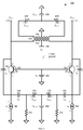
FIG. 1 schematically illustrates a circuit diagram for showing the configuration of a differential oscillator according to an example of the present invention; -
FIG. 2 schematically illustrates a circuit diagram for showing the configuration of a differential oscillator according to another example of the present invention; and -
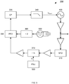
FIG. 3 schematically illustrates a circuit diagram of a PLL synthesizers according to another example of the present invention. - Embodiments of the present disclosure will be described below in detail with reference to drawings. Note that the same reference numerals are used to represent identical or equivalent elements in figures, and the description thereof will not be repeated. The embodiments set forth below represent the necessary information to enable those skilled in the art to practice the invention. Upon reading the following description in light of the accompanying drawing figures, those skilled in the art will understand the concepts of the invention and will recognize applications of these concepts not particularly addressed herein. It should be understood that these concepts and applications fall within the scope of the disclosure and the accompanying claims.
- With reference to
FIG. 1 , a schematic circuit diagram for showing a configuration of a differential oscillator according to an example of the present invention is illustrated. Thedifferential oscillator 100 is a common-base Colpitts oscillator and takes the form of a differential oscillator circuit with positive and negativeoutput terminals V out+ 110 andV out- 115. It should be noted that in the context of this specification, a differential signal may comprise two components having the same amplitude and opposite phase. A differential signal may be provided via two terminals. - The differential oscillator comprises two active devices, in this case
first transistor 130 andsecond transistor 135. Any kind of transistor or suitable active device may be used. The active devices respectivelytransistors bipolar transistors bipolar junction transistors - In the illustrated configuration, the
bipolar transistors bipolar transistors transistor biasing voltage source 160 coupled between the bases of thetransistors transistors transistors transistors -
Capacitors transistors capacitor 120 and thecapacitor 125 form positive feedback capacitors, each of which being connected to the collector and the emitter of a respective one of thetransistors capacitors transistors capacitors - A
coil 155 biased at asupply voltage V dd 140 is coupled to the collectors of thetransistors transistors coil 155. The collectors of thetransistors coil 155. In an example, asupply voltage V dd 140 is supplied to thecoil 155; in particular thesupply voltage V dd 140 is supplied to a center tap of thecoil 155. For instance, the supply voltage Vdd may be 2.5 V, or lower, or higher (e.g. 3.3 V or 5 V). - The emitters of the
transistors varactors varactors tuning voltage source 200 to supply an interconnection common net of thevaractors varactors varactors varactors transistors varactors - In order to enable the tuning voltage Vtune2 to tune the
varactor capacitors further capacitors transistors varactors capacitors capacitors resistors capacitors biasing resistors varactors - In the differential oscillator, a bias
current source 190 provides a bias current Ib1 for thetransistor 130 and a biascurrent source 195 provides a bias current Ib2 for thetransistor 135, respectively. The biascurrent sources current sources transistor current sources transistor - The positive and negative
output terminals V out+ 110 andV out- 115 are coupled to the collectors of the respective one of thetransistors - The
coil 155 is a first or primary coil of atransformer 150 comprising a second orsecondary coil 156 inductively coupled with thecoil 155. Thesecond coil 156 is coupled in series tovaractors tuning voltage source 230 to the common interconnection net of thevaractors varactors varactors varactors varactors second coil 156. The center tap of thesecond coil 156 is applied to a reference potential, and in particular, the center tap of thesecond coil 156 is set to lowest reference potential such as ground, in order to achieve a maximal tuning range within a given supply. - The main frequency tuning of the differential oscillator is enabled by the transformer coupled
varactor pair varactors varactors varactor pair - With respect to
FIG. 1 , an example of a differential oscillator is illustrated and described, which comprisesbipolar transistors bipolar transistors bipolar transistors - Referring now to
FIG. 2 , a schematic circuit diagram for showing another configuration of a differential oscillator according to an example of the present invention is illustrated. The active devices respectivelytransistors FIG. 1 . Hence, the above description essentially applies likewise to the configuration ofFIG. 2 provided that the technical terms relating to the terminals of thebipolar transistors - For the sake of description, the collector terminal and the drain terminal will be also referred to as a first current terminal, the emitter terminal and drain terminal will be also referred to as a second current terminal and the base terminal and gate terminal will be also referred to as a control terminal.
- With respect to
FIG. 3 , a schematic circuit diagram of a PLL synthesizer according to another example of the present invention is illustrated. The illustrated PLL synthesizer should be understood to represent a use case of the above described differential VCO, but the present application should not be understood to be limited thereto. - The PLL synthesizer comprises a divider chain receiving the output signal of the
differential VCO 100. The divider chain may comprise a static frequency divider, SFD, 310 and aprogrammable divider 310. The programmable divider may receive control information in form of a frequency control word from a frequency selection logic, FSL. The output of the divider chain is supplied to a phase and frequency detector, PFD, 330, which further receives a reference input signal, e.g. from a master oscillator, 300, and a downstream arranged fixed frequency divider, 305. The phase and frequency difference generated by the phase and frequency detector, PFD, 330 is supplied to a charge pump, CP, 335 and afilter 340, which finally generate the tuning voltage signal Vture1 for being supplied to thedifferential voltage oscillator 100. - According to an example of the present application, a differential oscillator circuit is provided. The differential oscillator circuit comprises a pair of transistors with control terminals biased by a common biasing voltage. The differential oscillator circuit further comprises a transformer having a primary coil coupled between first current terminals of the transistors and a secondary coil coupled in a closed series circuit with two varactors, which are arranged for being tuned by a first common tuning voltage. The differential oscillator circuit further comprises a series circuit comprising two further varactors coupled in series to second current terminals of the transistors. The two further varactors are arranged for being tuned by a second common tuning voltage.
- According to an example, the differential oscillator circuit further comprises feedback capacitors. Each of the feedback capacitors is coupled between the first and second current terminals of a respective one of the transistors.
- According to an example, the differential oscillator circuit further comprises bias current sources. Each of the bias current sources is inserted between the second current terminals of a respective one of the transistors and a reference potential (e.g. a lowest reference potential or ground). The bias current sources may supply direct currents, and in particular, the bias current sources may supply the same direct current to the second current terminals of a respective one of the transistors.
- According to an example, the transistors form a balanced differential pair.
- According to an example, the primary coil has a center tap, which is arranged to receive a supply voltage. According to an example, the secondary coil has a center tap, which is arranged receive the reference potential (e.g. a lowest reference potential or ground).
- According to an example, the transistors are bipolar transistors. The first current terminal is a collector terminal, the second current terminal is an emitter terminal, and the control terminal is a base terminal. According to an example, the transistors are bipolar transistors and in particular npn-transistors.
- According to an example, the transistors are metal-oxide semiconductor (MOS) transistors and in particular MOSFETs (metal-oxide semiconductor field effect transistors). The first current terminal is a drain terminal, the second current terminal is a source terminal, and the control terminal is a gate terminal. According to an example, the transistors are n-channel MOS transistors and n-channel MOSFETs.
- According to an example, the differential oscillator circuit further comprises two capacitors. Each of the two capacitors is coupled in series between the second current terminals of a respective one of the transistors and a respective one of the two further varactors.
- According to an example, the differential oscillator circuit further comprises two resistors. Each of the two resistors is coupled to an interconnection between a respective one of the two capacitors and an adjacent one of the two further varactors and reference potential (e.g. a lowest reference potential or ground).
- According to an example, the differential oscillator circuit further comprises a biasing voltage source coupled to an interconnection of the control terminals of the transistors and arranged to supply the common biasing voltage. The biasing voltage source is arranged to supply a common mode DC biasing voltage.
- According to an example, the differential oscillator circuit further comprises a first tuning voltage source coupled to an interconnection of the two varactors and arranged to supply the first common tuning voltage. The first tuning voltage source is arranged to supply a first common DC tuning voltage.
- According to an example, the differential oscillator circuit further comprises a second tuning voltage source coupled to an interconnection of the two further varactors and arranged to supply the second common tuning voltage. The second tuning voltage source is arranged to supply a second common DC tuning voltage.
- In the foregoing specification, the invention has been described with reference to specific examples of embodiments of the invention. It will, however, be evident that various modifications and changes may be made therein without departing from the broader spirit and scope of the invention as set forth in the appended claims.
- For example, the semiconductor substrate described herein can be any semiconductor material or combinations of materials, such as gallium arsenide, silicon germanium, silicon-on- insulator (SOI), silicon, monocrystalline silicon, the like, and combinations of the above.
- The connections or couplings as discussed herein may be any type of connection or coupling suitable to transfer signals from or to the respective nodes, units or devices, for example via intermediate devices. The terms coupling and connection, respectively coupled and connected, may be used interchangeably. Accordingly, unless implied or stated otherwise, the connections may for example be direct connections or indirect connections. The connections may be illustrated or described in reference to be a single connection, a plurality of connections, unidirectional connections, or bidirectional connections. However, different embodiments may vary the implementation of the connections. For example, separate unidirectional connections may be used rather than bidirectional connections and vice versa. Also, plurality of connections may be replaced with a single connection that transfers multiple signals serially or in a time multiplexed manner. Likewise, single connections carrying multiple signals may be separated out into various different connections carrying subsets of these signals. Therefore, many options exist for transferring signals.
- Each signal described herein may be designed as differential: positive or negative analog signal. In the case of a negative analog signal, the signal is relative lower than the common-mode DC signal, which corresponds to an analog ground level zero. In the case of a positive signal, the signal is higher than the common-mode DC signal, which corresponds to an analog ground. Note that any of the differential signals described herein can be designed as either negative or positive signals.
- Those skilled in the art will recognize that the boundaries between functional blocks are merely illustrative and that alternative embodiments may merge functional blocks or circuit elements or impose an alternate decomposition of functionality upon various blocks or circuit elements. Thus, it is to be understood that the architectures depicted herein are merely exemplary, and that in fact many other architectures can be implemented which achieve the same functionality. For example, an inductive coil and a resistor may be integrated into one element.
- Any arrangement of components to achieve the same functionality is effectively "associated" such that the desired functionality is achieved. Hence, any two components herein combined to achieve a particular functionality can be seen as "associated with" each other such that the desired functionality is achieved, irrespective of architectures or intermedial components. Likewise, any two components so associated can also be viewed as being "operably connected", or "operably coupled", to each other to achieve the desired functionality.
- Furthermore, those skilled in the art will recognize that boundaries between the above described operations merely illustrative. The multiple operations may be combined into a single operation, a single operation may be distributed in additional operations and operations may be executed at least partially overlapping in time. Moreover, alternative embodiments may include multiple instances of a particular operation, and the order of operations may be altered in various other embodiments.
- Also, the illustrated examples may be implemented as circuitry located on a single integrated circuit or within a same device, in an embodiment. For example, all the components of the oscillator circuit may be integrated on one substrate. Alternatively, the examples may be implemented as any number of separate integrated circuits or separate devices interconnected with each other in a suitable manner. For example, one or more than one of the output branches may be provided partially or completely on a substrate different from the substrate the oscillator core is provided on.
- Also, the examples, the embodiments, or portions thereof, may implemented as soft or code representations of physical circuitry or of logical representations convertible into physical circuitry, such as in a hardware description language of any appropriate type.
- Also, the invention is not limited to physical devices or units implemented in non- programmable hardware but can also be applied in programmable devices or units able to perform the desired device functions by operating in accordance with suitable program code, such as mainframes, minicomputers, servers, workstations, personal computers, notepads, personal digital assistants, electronic games, automotive and other embedded systems, cell phones and various other wireless devices, commonly denoted in this application as "computer systems".
- However, other modifications, variations and alternatives are also possible. The specifications and drawings are, accordingly, to be regarded in an illustrative rather than in a restrictive sense.
- In the claims, any reference signs placed between parentheses shall not be construed as limiting the claim. The word "comprising" does not exclude the presence of other elements or steps then those listed in a claim. Furthermore, the terms "a" or "an", as used herein, are defined as one or more than one. Also, the use of introductory phrases such as "at least one" and "one or more" in the claims should not be construed to imply that the introduction of another claim element by the indefinite articles "a" or "an" limits any particular claim containing such introduced claim element to inventions containing only one such element, even when the same claim includes the introductory phrases "one or more" or "at least one" and indefinite articles such as "a" or "an". The same holds true for the use of definite articles. Unless stated otherwise, terms such as "first" and "second" are used to arbitrarily distinguish between the elements such terms describe. Thus, these terms are not necessarily intended to indicate temporal or other prioritization of such elements. The mere fact that certain measures are recited in mutually different claims does not indicate that a combination of these measures cannot be used to advantage.
Claims (15)
- A differential oscillator circuit comprising:a pair of transistors (130, 130', 135, 135') with control terminals biased by a common biasing voltage (Vbias);a transformer (150) having a primary coil (155) coupled between first current terminals of the transistors (130, 130', 135, 135') and a secondary coil (156) coupled in a closed series circuit with two varactors (220, 225), which are arranged for being tuned by a first common tuning voltage (Vtune1); anda series circuit comprising two further varactors (170, 175) coupled in series to second current terminals of the transistors (130, 130', 135, 135'), wherein the two further varactors (170, 175) are arranged for being tuned by a second common tuning voltage (Vtune2).
- The circuit according to claim 1, further comprising:
feedback capacitors (120, 125), each of which coupled between the first and second current terminals of a respective one of the transistors (130, 130', 135, 135'). - The circuit according to claim 1 or claim 2, further comprising:
bias current sources (190, 195), each of which inserted between the second current terminals of a respective one of the transistors (130, 130', 135, 135') and a reference potential. - The circuit according to any preceding claim,
wherein the transistors (130, 130', 135, 135') form a balanced differential pair. - The circuit according to any preceding claim,
wherein the primary coil (155) has a center tap, which is arranged to receive a supply voltage (Vdd). - The circuit according to any preceding claim,
wherein the secondary coil (156) has a center tap, which is supplied to the reference potential. - The circuit according to any preceding claim,
wherein the transistors (130, 135) are bipolar transistors, wherein the first current terminal is a collector terminal, the second current terminal is an emitter terminal and the control terminal is a base terminal. - The circuit according to claim 7,
wherein the transistors (130, 135) are npn-transistors. - The circuit according to any one of the claims 1 to 6,
wherein the transistors (130', 135') are metal-oxide semiconductor, MOS, transistors, wherein the first current terminal is a drain terminal, the second current terminal is a source terminal and the control terminal is a gate terminal. - The circuit according to claim 9,
wherein the transistors (130', 135') are n-channel MOS transistors. - The circuit according to any preceding claim, further comprising:
two capacitors (180, 185), each of which coupled in series between the second current terminals of a respective one of the transistors (130, 130', 135, 135') and a respective one of the two further varactors (170, 175). - The circuit according to claim 11, further comprising:
two resistors (210, 215), each of which coupled to an interconnection between a respective one of the two capacitors (180, 185) and an adjacent one of the two further varactors (170, 175) and base reference potential. - The circuit according to any preceding claim, further comprising:
a biasing voltage source (160) coupled to an interconnection of the control terminals of the transistors (130, 130', 135, 135') and arranged to supply the common biasing voltage (Vbias). - The circuit according to any preceding claim, further comprising:
a first tuning voltage source (230) coupled to an interconnection of the two varactors (220, 225) and arranged to supply the first common tuning voltage (Vtune1). - The circuit according to any preceding claim, further comprising:
a second tuning voltage source (200) coupled to an interconnection of the two further varactors (170, 175) and arranged to supply the second common tuning voltage (Vtune2).
Priority Applications (3)
| Application Number | Priority Date | Filing Date | Title |
|---|---|---|---|
| EP18305691.0A EP3579407A1 (en) | 2018-06-06 | 2018-06-06 | Differential voltage-controlled (vco) oscillator |
| US16/427,455 US10826431B2 (en) | 2018-06-06 | 2019-05-31 | Differential voltage-controlled (VCO) oscillator |
| CN201910483666.XA CN110572155A (en) | 2018-06-06 | 2019-06-05 | Differential Voltage Controlled (VCO) Oscillator |
Applications Claiming Priority (1)
| Application Number | Priority Date | Filing Date | Title |
|---|---|---|---|
| EP18305691.0A EP3579407A1 (en) | 2018-06-06 | 2018-06-06 | Differential voltage-controlled (vco) oscillator |
Publications (1)
| Publication Number | Publication Date |
|---|---|
| EP3579407A1 true EP3579407A1 (en) | 2019-12-11 |
Family
ID=62715986
Family Applications (1)
| Application Number | Title | Priority Date | Filing Date |
|---|---|---|---|
| EP18305691.0A Withdrawn EP3579407A1 (en) | 2018-06-06 | 2018-06-06 | Differential voltage-controlled (vco) oscillator |
Country Status (3)
| Country | Link |
|---|---|
| US (1) | US10826431B2 (en) |
| EP (1) | EP3579407A1 (en) |
| CN (1) | CN110572155A (en) |
Families Citing this family (2)
| Publication number | Priority date | Publication date | Assignee | Title |
|---|---|---|---|---|
| EP3836401A1 (en) | 2019-12-10 | 2021-06-16 | NXP USA, Inc. | Frequency synthesizer with phase noise temperature compensation, communication unit and method therefor |
| CN111948662B (en) * | 2020-08-13 | 2023-07-21 | 重庆大学 | A dynamic ranging method based on optimization method for anti-frequency drift sweeping interference |
Citations (7)
| Publication number | Priority date | Publication date | Assignee | Title |
|---|---|---|---|---|
| US20040196110A1 (en) * | 2003-04-04 | 2004-10-07 | Vito Boccuzzi | Differently-tuned VCO using inductively coupled varactors |
| US6946924B2 (en) * | 2002-08-14 | 2005-09-20 | International Business Machines Corporation | Low noise voltage controlled oscillator |
| US20080106343A1 (en) * | 2006-11-07 | 2008-05-08 | National Taiwan University Of Science And Technology | Multi-phase voltage-control oscillator |
| US20100123536A1 (en) * | 2008-11-19 | 2010-05-20 | Yumin Lu | Tunable capacitively loaded transformer providing switched inductance for rf/microwave integrated circuits |
| US20110043401A1 (en) * | 2008-05-13 | 2011-02-24 | Freescale Semiconductor, Inc. | Voltage-controlled oscillator and radar system |
| US8489054B2 (en) * | 2010-03-16 | 2013-07-16 | Stmicroelectronics S.R.L. | Millimeter wave oscillator |
| WO2018023367A1 (en) * | 2016-08-02 | 2018-02-08 | 华为技术有限公司 | Voltage waveform shaping oscillator |
Family Cites Families (4)
| Publication number | Priority date | Publication date | Assignee | Title |
|---|---|---|---|---|
| US7154349B2 (en) | 2004-08-11 | 2006-12-26 | Qualcomm, Incorporated | Coupled-inductor multi-band VCO |
| ITVA20070009A1 (en) * | 2007-01-17 | 2008-07-18 | St Microelectronics Srl | METHOD OF ADJUSTING THE FREQUENCY OF RESONANCE OF AN LC RESONANT CIRCUIT AND ITS RESONANT CIRCUIT |
| US8749316B2 (en) * | 2009-06-23 | 2014-06-10 | Qualcomm Incorporated | Programmable varactor and methods of operation thereof |
| US9461583B2 (en) * | 2015-01-08 | 2016-10-04 | Infineon Technologies Ag | System and method for a voltage controlled oscillator |
-
2018
- 2018-06-06 EP EP18305691.0A patent/EP3579407A1/en not_active Withdrawn
-
2019
- 2019-05-31 US US16/427,455 patent/US10826431B2/en active Active
- 2019-06-05 CN CN201910483666.XA patent/CN110572155A/en not_active Withdrawn
Patent Citations (8)
| Publication number | Priority date | Publication date | Assignee | Title |
|---|---|---|---|---|
| US6946924B2 (en) * | 2002-08-14 | 2005-09-20 | International Business Machines Corporation | Low noise voltage controlled oscillator |
| US20040196110A1 (en) * | 2003-04-04 | 2004-10-07 | Vito Boccuzzi | Differently-tuned VCO using inductively coupled varactors |
| US20080106343A1 (en) * | 2006-11-07 | 2008-05-08 | National Taiwan University Of Science And Technology | Multi-phase voltage-control oscillator |
| US20110043401A1 (en) * | 2008-05-13 | 2011-02-24 | Freescale Semiconductor, Inc. | Voltage-controlled oscillator and radar system |
| US20100123536A1 (en) * | 2008-11-19 | 2010-05-20 | Yumin Lu | Tunable capacitively loaded transformer providing switched inductance for rf/microwave integrated circuits |
| US8489054B2 (en) * | 2010-03-16 | 2013-07-16 | Stmicroelectronics S.R.L. | Millimeter wave oscillator |
| WO2018023367A1 (en) * | 2016-08-02 | 2018-02-08 | 华为技术有限公司 | Voltage waveform shaping oscillator |
| EP3442118A1 (en) * | 2016-08-02 | 2019-02-13 | Huawei Technologies Co., Ltd. | Voltage waveform shaping oscillator |
Non-Patent Citations (1)
| Title |
|---|
| ZIRATH H ET AL: "MMIC-oscillator designs for ultra low phase noise", COMPOUND SEMICONDUCTOR INTEGRATED CIRCUIT SYMPOSIUM, 2005. CSIC '05. I EEE PALM SPRINGS, CA, USA 30 OCT. - 2 NOV. 2005, PISCATAWAY, NJ, USA,IEEE, 30 October 2005 (2005-10-30), pages 204 - 207, XP010852492, ISBN: 978-0-7803-9250-2, DOI: 10.1109/CSICS.2005.1531813 * |
Also Published As
| Publication number | Publication date |
|---|---|
| US20190379326A1 (en) | 2019-12-12 |
| CN110572155A (en) | 2019-12-13 |
| US10826431B2 (en) | 2020-11-03 |
Similar Documents
| Publication | Publication Date | Title |
|---|---|---|
| US7298183B2 (en) | High frequency divider circuits and methods | |
| US7522007B2 (en) | Injection locked frequency divider | |
| US7710211B2 (en) | Injection-locked frequency divider with a wide injection-locked frequency range | |
| US8085087B2 (en) | Switched capacitor circuit capable of minimizing clock feedthrough effect and having low phase noise and method thereof | |
| US7592875B2 (en) | Injection-locked oscillator circuit | |
| EP2201686B1 (en) | Voltage controlled oscillator with cascaded emitter follower buffer stages | |
| US20190372576A1 (en) | Dual voltage controlled oscillator circuits for a broadband phase locked loop for multi-band millimeter-wave 5g communication | |
| US7332951B2 (en) | Switched capacitor circuit capable of minimizing clock feedthrough effect and having low phase noise and method thereof | |
| CN105790759A (en) | System And Method For A Voltage Controlled Oscillator | |
| TWI489767B (en) | Oscillator circuit | |
| US10826431B2 (en) | Differential voltage-controlled (VCO) oscillator | |
| US9344035B2 (en) | System and method for a voltage controlled oscillator | |
| US10938345B2 (en) | Gm-boosted differential voltage-controlled oscillator (VCO) | |
| US20050206434A1 (en) | Switched capacitor circuit capable of minimizing clock feedthrough effect and having low phase noise and method thereof | |
| US20160072436A1 (en) | Method and Apparatus of Synchronizing Oscillators | |
| Wang et al. | A 20GHz VCO and frequency doubler for W-band FMCW radar applications | |
| US9106179B2 (en) | Voltage-controlled oscillators and related systems | |
| WO2013085971A1 (en) | An injection locked divider with injection point located at a tapped inductor | |
| US7741926B2 (en) | Frequency synthesizer having improved frequency hopping | |
| US20130141178A1 (en) | Injection Locked Divider with Injection Point Located at a Tapped Inductor | |
| Bhavsar et al. | Low Noise L band PLL-VCO designed for the IRNSS-Rx using BiCMOS 180 nm Process | |
| Jacquemod et al. | Comparison between RTW VCO and LC QVCO 12 GHz PLLs | |
| Pawar et al. | Design and Implementation of Ku Band LC-VCO using 90nm CMOS Process | |
| KR102273842B1 (en) | Temperature compensated LC oscillator | |
| US20110043293A1 (en) | DeMOS VCO |
Legal Events
| Date | Code | Title | Description |
|---|---|---|---|
| PUAI | Public reference made under article 153(3) epc to a published international application that has entered the european phase |
Free format text: ORIGINAL CODE: 0009012 |
|
| STAA | Information on the status of an ep patent application or granted ep patent |
Free format text: STATUS: THE APPLICATION HAS BEEN PUBLISHED |
|
| AK | Designated contracting states |
Kind code of ref document: A1 Designated state(s): AL AT BE BG CH CY CZ DE DK EE ES FI FR GB GR HR HU IE IS IT LI LT LU LV MC MK MT NL NO PL PT RO RS SE SI SK SM TR |
|
| AX | Request for extension of the european patent |
Extension state: BA ME |
|
| STAA | Information on the status of an ep patent application or granted ep patent |
Free format text: STATUS: REQUEST FOR EXAMINATION WAS MADE |
|
| 17P | Request for examination filed |
Effective date: 20200612 |
|
| RBV | Designated contracting states (corrected) |
Designated state(s): AL AT BE BG CH CY CZ DE DK EE ES FI FR GB GR HR HU IE IS IT LI LT LU LV MC MK MT NL NO PL PT RO RS SE SI SK SM TR |
|
| STAA | Information on the status of an ep patent application or granted ep patent |
Free format text: STATUS: EXAMINATION IS IN PROGRESS |
|
| 17Q | First examination report despatched |
Effective date: 20210922 |
|
| STAA | Information on the status of an ep patent application or granted ep patent |
Free format text: STATUS: THE APPLICATION HAS BEEN WITHDRAWN |
|
| 18W | Application withdrawn |
Effective date: 20220110 |