EP3579272A1 - Electronic device - Google Patents
Electronic device Download PDFInfo
- Publication number
- EP3579272A1 EP3579272A1 EP19176094.1A EP19176094A EP3579272A1 EP 3579272 A1 EP3579272 A1 EP 3579272A1 EP 19176094 A EP19176094 A EP 19176094A EP 3579272 A1 EP3579272 A1 EP 3579272A1
- Authority
- EP
- European Patent Office
- Prior art keywords
- signal
- electronic device
- disposed
- pads
- light
- Prior art date
- Legal status (The legal status is an assumption and is not a legal conclusion. Google has not performed a legal analysis and makes no representation as to the accuracy of the status listed.)
- Withdrawn
Links
Images




Classifications
-
- H—ELECTRICITY
- H05—ELECTRIC TECHNIQUES NOT OTHERWISE PROVIDED FOR
- H05K—PRINTED CIRCUITS; CASINGS OR CONSTRUCTIONAL DETAILS OF ELECTRIC APPARATUS; MANUFACTURE OF ASSEMBLAGES OF ELECTRICAL COMPONENTS
- H05K1/00—Printed circuits
- H05K1/02—Details
- H05K1/0296—Conductive pattern lay-out details not covered by sub groups H05K1/02 - H05K1/0295
- H05K1/0298—Multilayer circuits
-
- H—ELECTRICITY
- H10—SEMICONDUCTOR DEVICES; ELECTRIC SOLID-STATE DEVICES NOT OTHERWISE PROVIDED FOR
- H10W—GENERIC PACKAGES, INTERCONNECTIONS, CONNECTORS OR OTHER CONSTRUCTIONAL DETAILS OF DEVICES COVERED BY CLASS H10
- H10W90/00—Package configurations
-
- H—ELECTRICITY
- H05—ELECTRIC TECHNIQUES NOT OTHERWISE PROVIDED FOR
- H05K—PRINTED CIRCUITS; CASINGS OR CONSTRUCTIONAL DETAILS OF ELECTRIC APPARATUS; MANUFACTURE OF ASSEMBLAGES OF ELECTRICAL COMPONENTS
- H05K1/00—Printed circuits
- H05K1/02—Details
- H05K1/0274—Optical details, e.g. printed circuits comprising integral optical means
-
- H—ELECTRICITY
- H05—ELECTRIC TECHNIQUES NOT OTHERWISE PROVIDED FOR
- H05K—PRINTED CIRCUITS; CASINGS OR CONSTRUCTIONAL DETAILS OF ELECTRIC APPARATUS; MANUFACTURE OF ASSEMBLAGES OF ELECTRICAL COMPONENTS
- H05K1/00—Printed circuits
- H05K1/02—Details
- H05K1/11—Printed elements for providing electric connections to or between printed circuits
-
- H—ELECTRICITY
- H05—ELECTRIC TECHNIQUES NOT OTHERWISE PROVIDED FOR
- H05K—PRINTED CIRCUITS; CASINGS OR CONSTRUCTIONAL DETAILS OF ELECTRIC APPARATUS; MANUFACTURE OF ASSEMBLAGES OF ELECTRICAL COMPONENTS
- H05K1/00—Printed circuits
- H05K1/18—Printed circuits structurally associated with non-printed electric components
- H05K1/181—Printed circuits structurally associated with non-printed electric components associated with surface mounted components
-
- H—ELECTRICITY
- H10—SEMICONDUCTOR DEVICES; ELECTRIC SOLID-STATE DEVICES NOT OTHERWISE PROVIDED FOR
- H10H—INORGANIC LIGHT-EMITTING SEMICONDUCTOR DEVICES HAVING POTENTIAL BARRIERS
- H10H20/00—Individual inorganic light-emitting semiconductor devices having potential barriers, e.g. light-emitting diodes [LED]
- H10H20/80—Constructional details
- H10H20/83—Electrodes
- H10H20/831—Electrodes characterised by their shape
-
- H—ELECTRICITY
- H10—SEMICONDUCTOR DEVICES; ELECTRIC SOLID-STATE DEVICES NOT OTHERWISE PROVIDED FOR
- H10H—INORGANIC LIGHT-EMITTING SEMICONDUCTOR DEVICES HAVING POTENTIAL BARRIERS
- H10H20/00—Individual inorganic light-emitting semiconductor devices having potential barriers, e.g. light-emitting diodes [LED]
- H10H20/80—Constructional details
- H10H20/85—Packages
- H10H20/857—Interconnections, e.g. lead-frames, bond wires or solder balls
Definitions
- Embodiments of the present disclosure relate to an electronic device, and in particular they relate to an electronic device including a conductive structure.
- the present disclosure is to provide an electronic device designed to have a larger size, high resolution, thin or narrow frame, for example a tiled electronic device.
- an electronic device includes a first substrate, a first conductive layer, a plurality of first electrode pads, a plurality of first light-emitting units, a plurality of first signal pads and a conductive structure.
- the first conductive layer is disposed on the first substrate.
- the first electrode pads are disposed on the first conductive layer.
- the first light-emitting units overlap and are disposed on the first electrode pads.
- the first light-emitting units are electrically connected to the first electrode pads respectively.
- the first signal pads are disposed on the first conductive layer and electrically connected to the first conductive layer.
- the conductive structure is disposed on the first signal pads, and at least two of the first signal pads are electrically connected to each other through the conductive structure.
- a first feature is disposed on (or formed on) a second feature in the description that follows may include embodiments in which the first feature and second feature are disposed (or formed) in direct contact, and may also include embodiments in which additional features may be disposed (or formed) between the first feature and second feature, so that the first feature and second feature may not be in direct contact.
- spatially relative terms such as “beneath,” “below,” “lower,” “on,” “above,” “upper” and the like, may be used herein for ease of description to describe one element or feature's relationship to other elements or features as illustrated in the figures.
- the spatially relative terms are intended to encompass different orientations of the device in use or operation in addition to the orientation depicted in the figures.
- the apparatus may be otherwise oriented (rotated 45 degrees or at other orientations) and the spatially relative descriptors used herein may likewise be interpreted accordingly.
- the terms “about” and “substantially” typically mean +/-20% of the stated value, more typically +/-10% of the stated value, more typically +/-5% of the stated value, more typically +/-3% of the stated value, more typically +/-2% of the stated value, more typically +/-1% of the stated value and even more typically +/-0.5% of the stated value.
- the stated value of the present disclosure is an approximate value. That is, when there is no specific description of the terms “about” and “substantially”, the stated value includes the meaning of "about” or “substantially”.
- first,” “second,” “third,” etc. can be used herein to describe various elements, components, regions, layers and/or sections, these elements, components, regions, layers and/or sections should not be limited through these terms. These terms are only used to distinguish one element, component, region, layer or section from another region, layer or section. Thus, a first element, component, region, layer or section discussed below could be termed a second element, component, region, layer or section without departing from the teachings of the present disclosure.
- the elements in the drawings are merely illustrative, and the dimensions (including length, width, or height) of the elements should not be limited in the drawings.
- the electronic device described in the present disclosure may include a display device, a light-emitting device, a detecting device, a touch device, or other suitable device, but the disclosed embodiments are not limited thereto.
- FIG. 1 is a partial top view illustrating an electronic device 100 according to one embodiment of the present disclosure.
- FIG. 2 is a partial top view illustrating a tiled electronic device 101 according to one embodiment of the present disclosure.
- FIG. 3 is a partial cross-sectional view illustrating the tiled electronic device 101 along line A-A' and line B-B' in FIG. 1 .
- the electronic device 100 may include a substrate, and in the embodiment as shown in FIG.2 , the tiled electronic device 101 may include a plurality of substrates.
- the corresponding positions or the materials of the elements (or layers) on the substrate of the electronic device 100 may be the same as or be similar to the corresponding elements (or layers) disposed on the plurality of substrates of the tiled electronic device 101.
- the elements (or layers) mentioned above may include conductive layers, electrode pads, light-emitting units, signal pads or other suitable elements (or layers), which may refer to the following embodiments (as shown in FIG. 1 to FIG. 3 ) in more detail. Therefore, the cross-sectional view of the electronic device 100 may also refer to the cross-sectional view as shown in FIG. 3 .
- the electronic device 100 includes a first substrate 11, a first conductive layer 21, a plurality of first electrode pads 31, a plurality of first light-emitting units 41, a plurality of first signal pads 51 and a conductive structure 60.
- the first conductive layer 21 may be electrically connected to the plurality of first electrode pads 31 and the plurality of first signal pads 51, respectively.
- the first substrate 11 may be an array substrate, and the first conductive layer 21 may be disposed (or formed) on the first substrate 11.
- the first conductive layer 21 may be used as the conductive line for transmitting voltage signals.
- the material of the first conductive layer 21 may include metals (e.g., copper, molybdenum, aluminum, tungsten, gold, chromium, nickel, platinum, titanium), alloys (e.g., alloys of the above metals), transparent conductive materials, other suitable conductive materials, or a combination thereof, but it is not limited thereto.
- the transparent conductive materials may include indium tin oxide (ITO), tin oxide (TO), indium zinc oxide (IZO), indium gallium zinc oxide (IGZO), antimony-doped tin oxide (ATO), aluminium-doped zinc oxide (AZO), but it is not limited thereto.
- the first conductive layer 21 may include a single-layer material, a multi-layer material or a composite material.
- the first electrode pads 31 are disposed on the first conductive layer 21, the first light-emitting units 41 overlap and are disposed on the first electrode pads 31, and the first light-emitting units 41 are electrically connected to the first electrode pads 31, respectively.
- the cathode (and/or anode) of the first light-emitting unit 41 may be electrically connected to the first conductive layer 21 through the first electrode pads 31. That is, the first electrode pads 31 may be used as the pads of the first light-emitting units 41.
- the first light-emitting units 41 may include light-emitting diodes (LED), micro LED, mini LED, quantum dot light-emitting diodes (QLED/QDLED), quantum dots or other suitable components, but it is not limited thereto.
- the first light-emitting units 41 may include organic light-emitting diodes (OLED), but it is not limited thereto.
- the first signal pads 51 are disposed on the first conductive layer 21 and electrically connected to the first conductive layer 21, the conductive structure 60 is disposed on the first signal pads 51, and at least two of the first signal pads 51 are electrically connected to each other through the conductive structure 60 as shown in FIG. 3 .
- the first signal pads 51 are disposed between the conductive structure 60 and the first conductive layer 21 in the Z-direction (i.e., the normal direction of the first substrate 11), and the conductive structure 60 is electrically connected to the first conductive layer 21 through the first signal pads 51 as shown in FIG. 1 and FIG. 3 .
- the conductive structure 60 may overlap at least part of the first signal pads 51 in the Z-direction.
- the conductive structure 60 is electrically connected to the circuit board 70 as shown in FIG. 1 or voltage-signal supply circuits (not shown).
- the circuit board 70 may include a flexible printed circuit (FPC), a chip on film (COF) or a printed circuit board (PCB), but it is not limited thereto.
- the circuit board 70 may be electrically connected to the first conductive layer 21 through a conductive pad 80 (see FIG. 3 ).
- the circuit board 70 is disposed on the first substrate 11, at least one voltage signal transmitted through (or supplied from) the circuit board 70 may be transmitted to the first conductive layer 21 through the conductive structure 60, and the voltage signal may be transmitted to the first light-emitting units 41 through the first conductive layer 21.
- the first light-emitting units 41 may modulate the light to be emitted or the brightness of the light according to the received voltage signal, but the present disclosure is not limited thereto.
- the voltage signal mentioned above may include a supply voltage (e.g., VDD, VSS), a bias voltage, a reset voltage, a ground voltage (GND), or another suitable voltage signal, but it is not limited thereto.
- the first signal pads 51 may be used as power pads, but it is not limited thereto.
- the material of the first electrode pads 31 may be the same as the material of the signal pads 51, or the material of the first electrode pads 31 may be different from the material of the signal pads 51.
- the material of the first electrode pads 31 (or the material of the signal pads 51) may include nickel, copper, gold, tin, silver, other suitable conductive materials, alloys of the above metals or a combination thereof, but it is not limited thereto. It should be noted that the connecting relationship between the first signal pads 51 and the first conductive layer 21 is not limited to that as shown in FIG. 3 . Other suitable conductive materials may be disposed between the first signal pads 51 and the first conductive layer 21.
- the voltage signals transmitted through (or supplied from) the circuit board 70 may be transmitted to the light-emitting units (e.g., the first light-emitting units 41) by the conductive structure 60 with low impedance, which can enhance the transmission efficiency of the voltage signal or reduce the number of circuit boards 70.
- the impedance of the conductive structure 60 may be lowered by increasing the thickness T of the conductive layer 60 as shown in FIG. 3 , or by using a low-impedance material (e.g., gold, silver, copper) in the conductive layer 60, but the present disclosure is not limited thereto.
- the thickness T of the conductive layer 60 may be greater than or equal to the thickness T2 of the first conductive layer 21 as shown in FIG.
- the thickness T of the conductive layer 60 may be defined by a maximum thickness of the conductive layer 60 in the Z-direction, and the thickness T2 of the first conductive layer 21 may be defined by a minimum thickness of the first conductive layer 21 in the Z-direction. The detailed measurement method of the above thicknesses will be described later.
- the first substrate 11 may be divided into a first region 11-1 and a second region 11-2, and the first region 11-1 may be adjacent to (or surround) the second region 11-2 as show in FIG. 1 .
- the first region 11-1 may be a non-operating region (or non-display region), while the second region 11-2 may be an operating region (or display region).
- the outermost first light-emitting units may respectively has at least one side edge closest to the edge of the first substrate 11 as shown in FIG. 1 .
- the connected lines (such as the dashed-lines shown in FIG.
- the first light-emitting units 41 may include the light-emitting diodes, micro LED, mini LED or quantum dot light-emitting diodes, the profile of the first light-emitting unit 41 may be defined by the boundary of the first light-emitting unit 41 projecting on the first substrate 11 in the Z-direction, but it is not limited thereto, and the side edges closest to the edge of the first substrate 11 may be obtained from the profile.
- the profile of the first light-emitting units 41 may be defined by the boundary of the uppermost layers (or elements) included in the first light-emitting units 41 projecting on the first substrate 11 in the Z-direction, but it is not limited thereto, and the side edges closest to the edge of the first substrate 11 may be obtained from such profile.
- one of the first light-emitting units 41 may include a cathode electrode, an anode electrode or a light-emitting layer, but it is not limited thereto.
- the first light-emitting units 41 include organic light-emitting diodes, and the boundary of the first light-emitting units 41 may be defined by a pixel defining layer (PDL), but it is not limited thereto.
- the pixel defining layer (now shown) may be disposed on the first substrate 11, and the pixel defining layer may have a plurality of openings.
- the first light-emitting units 41 may respectively be disposed corresponding to or overlap the openings of the pixel defining layer.
- the projecting area of the openings of the pixel defining layer on the first substrate 11 may be defined as the profile of the first light-emitting units 41, but it is not limited thereto.
- the first light-emitting units 41 may be disposed corresponding to (or overlap) the second region 11-2 of the first substrate 11. That is, the first light-emitting units 41 may be disposed in the second region 11-2.
- the conductive structure 60 may be disposed corresponding to (or overlap) the first region 11-1 of the first substrate 11. That is, the conductive structure 60 may be disposed in the first region 11-1, but it is not limited thereto.
- the conductive structure 60 may have at least one openings O, and the openings O may be disposed corresponding to (or overlap) the second region 11-2 as shown in FIG. 1 ; or the openings O may overlap at least one of the first light-emitting units 41. In some embodiments, at least part of the conductive structure 60 may overlap at least one of the first light-emitting units 41.
- the electronic device 101 may be a tiled electronic device.
- the electronic device 101 includes a first substrate 11, a first conductive layer 21, a plurality of first electrode pads 31, a plurality of first light-emitting units 41, a plurality of first signal pads 51 and a conductive structure 60.
- the electronic device 101 further includes a second substrate 12, a second conductive layer 22, a plurality of second electrode pads 32, a plurality of second light-emitting units 42 and a plurality of second signal pads 52.
- the second substrate 12 may be an array substrate.
- the second conductive layer 22 may be disposed (or formed) on the second substrate 12, and the second conductive layer 22 may be electrically connected to the plurality of second electrode pads 32 and the plurality of second signal pads 52.
- the material of the second conductive layer 22, the material of the second electrode pads 32, and/or the material of the second signal pads 52 may be the same as or different from the material of the first conductive layer 21, the material of the first electrode pads 31, and/or the material of the first signal pads 51, respectively.
- the second electrode pads 32 are disposed on the second conductive layer 22, the second light-emitting units 42 may overlap (or be disposed on) the second electrode pads 32, and the second light-emitting units 42 are electrically connected to the second electrode pads 32 respectively.
- the second electrode pads 32 may be used as the pads of the second light-emitting units 42, and the second light-emitting units 42 may be electrically connected to the second conductive layer 22 through the second electrode pads 32.
- the second signal pads 52 are disposed on the second conductive layer 22, and the second signal pads 52 are electrically connected to the second conductive layer 22, the conductive structure 60 is disposed on the second signal pads 52, and at least two of the second signal pads 52 are electrically connected to each other through the conductive structure 60 as shown in FIG. 3 .
- the second signal pads 52 are disposed between the conductive structure 60 and the second conductive layer 22 in the Z-direction (i.e., the normal direction of the second substrate 12).
- the conductive structure 60 is electrically connected to the second conductive layer 22 through the second signal pads 52 as shown in FIG. 2 and FIG. 3 .
- the conductive structure 60 may overlap at least part of the second signal pads 52 in the Z-direction.
- the second substrate 12 may be divided into a first region 12-1 and a second region 12-2, and the first region 12-1 may be adjacent to (or surround) the second region 12-2.
- the first region 12-1 of the second substrate 12 may be a non-operating region (or non-display region), the second region 12-2 of the second substrate 12 may be an operating region (or display region).
- the definition of the first region 12-1 of the second substrate 12 and the definition of the second region 12-2 of the second substrate 12 may be similar to the definition of the first region 11-1 of the first substrate 11 and the definition of the second region 11-2 of the first substrate 11, which will not be repeated here. As shown in FIG.
- the second light-emitting units 42 may be disposed corresponding to (or overlap) the second region 12-2 of the second substrate 12. That is, the second light-emitting units 42 may be disposed in the second region 12-2.
- the conductive structure 60 may be disposed corresponding to (or overlap) the first region 12-1 of the second substrate 12. That is, the conductive structure 60 may be disposed in the first region 12-1, but it is not limited thereto.
- the second signal pads 52 may be disposed corresponding to (or overlap) the first region 12-1. That is, the second signal pads 52 may be disposed in the first region 12-1, but it is not limited thereto.
- the conductive structure 60 may have at least one openings O, and the openings O may be disposed corresponding to (or overlap) the second region 11-2 and/or the second region 12-2 as shown in FIG. 2 ; or the openings O may overlap at least one of the first light-emitting units 41 and/or at least one of the second light-emitting units 42. In some embodiments, at least one portion of the conductive structure 60 may overlap at least one of the second light-emitting units 42.
- the circuit board 70 may be electrically connected to at least one of the first signal pads 51 and at least one of the second signal pads 52 through conductive structure 60.
- at least one voltage signal transmitted through (or supplied from) the circuit board 70 may be transmitted to the first conductive layer 21 and/or the second conductive layer 22 through the conductive structure 60, and the voltage signals may be transmitted to the first light-emitting units 41 through the first conductive layer 21, and the voltage signals may be transmitted to the second light-emitting units 42 through the second conductive layer 22, but it is not limited thereto.
- the second signal pads 52 may be used to connect the conductive structure 60 to the second conductive layer 22. In some embodiments, the second signal pads 52 may be used as power pads, but it is not limited thereto.
- the connecting relationships between various elements (or layers) or the materials of various elements (or layers) disposed on the second substrate 12 may be the same as or similar to those disposed on the first substrate 11, except for the conductive structure.
- the elements (or layers) mentioned above may include the conductive layer, the electrode pads, the light-emitting units, the signal pads or other suitable elements (or layers).
- the electronic device 101 having four substrates is used as an example, but the present disclosure is not limited thereto.
- the electronic device may be a tiled electronic device having more or fewer substrates.
- the number and arrangement of the substrates (including the first substrate 11 or the second substrate 12), the light-emitting units (including the first light-emitting units 41 or the second light-emitting units 42), the signal pads (including the first signal pads 51 or the second signal pads 52) or other elements as shown in the figures of the present disclosure are examples only, and the present disclosure is not limited thereto.
- the substrates (including the first substrate 11 or the second substrate 12) as shown in the figures of the present disclosure are illustrated to be rectangular, but those are examples.
- the shape of substrates may include curved, polygonal, obtuse, acute or irregular shapes.
- the number of the circuit boards 70, the position of the circuit boards 70 or the way for electrically connecting the circuit boards 70 and the conductive structure 60 are not limited to the embodiments as shown in FIG. 1 and FIG. 2 .
- the circuit boards 70 may be in direct contact with the conductive structure 60, and the circuit boards 70 may be electrically connected to the conductive structure 60; or the circuit boards 70 may be electrically connected to the conductive structure 60 by other conductive elements (e.g., the circuit structure LS), which will be described in following FIG. 6 and FIG. 7 .
- the conductive structure 60 may be manufactured by inkjet printing or net technology, and may be disposed on the first signal pads 51 and the second signal pads 52 by compression, welding or laser heating, but the present disclosure is not limited thereto.
- the electronic device 101 may include a protective layer CL, and the protective layer CL may be disposed on the conductive structure 60 as shown in FIG. 3 .
- the protective layer CL may cover the conductive structure 60, and not overlap or cover the light-emitting units (such as the first light-emitting units 41 and the second light-emitting units 42), but it is not limited thereto.
- the protective layer CL may cover a portion of an insulating layer IL, and the insulating layer IL may be disposed between the first conductive layer 21 and the first light-emitting units 41.
- the insulating layer IL may be disposed between the second conductive layer 22 and the second light-emitting units 42, but it is not limited thereto.
- the material of the protective layer CL may include an absorption material, a light-shielding material, a material having buffering feature, a material having protective feature or a combination thereof, but it is not limited thereto.
- the material of the protective layer CL may be water-proof, antistatic or antifouling.
- the protective layer CL may include a single-layer material, a multi-layer material or a composite material.
- the thickness T4 of the protective layer CL may be less than or equal to the thickness T of the conductive structure 60.
- the thickness T4 of the protective layer CL may be greater than or equal to the thickness T of the conductive structure 60.
- the thickness T4 of the protective layer CL may be defined by a minimum thickness of the protective layer CL in the Z-direction.
- the material of the protective layer CL may include a transparent material, and at least part of the protective layer CL may overlap or not overlap the light-emitting units.
- FIG. 4 is a partial top view illustrating an electronic device 102 according to another embodiment of the present disclosure.
- FIG. 5 is a partial cross-sectional view illustrating the electronic device 102 along line C-C' in FIG. 4 .
- the embodiment as shown in FIG. 4 is similar to the embodiment as shown in FIG. 1 .
- the first substrate 11 may be divided into a first region 11-1 and a second region 11-2, and the plurality of first light-emitting units 41 may be disposed corresponding to the second region 11-2.
- the differences between the embodiment as shown in FIG. 4 and the embodiment as shown in FIG. 1 is that the conductive structure 60 of the electronic device 102 may be disposed corresponding to (or overlap) the first region 11-1 and the second region 11-2. That is, the conductive structure 60 may be disposed in first region 11-1 and the second region 11-2.
- the conductive structure 60 may be divided into a first portion 61 and a second portion 62 as shown in FIG. 4 and FIG. 5 .
- the first portion 61 may be disposed corresponding to (or overlap) the first region 11-1. That is, the first portion 61 may be disposed in the first region 11-1.
- the second portion 62 may be disposed corresponding to (or overlap) the second region 11-2. That is, the second portion 62 may be disposed in the second region 11-2.
- the second portion 62 of the conductive structure 60 may include at least one signal line SL.
- the signal lines SL may extend along the X-direction, but it is not limited thereto. In other embodiments (e.g., the embodiment as shown in following FIG. 9 ), the signal lines SL may extend along the Y-direction or other directions.
- the material of the signal line SL may include a material having low impedance, but it is not limited thereto.
- the material of the signal line SL may include metals (e.g., gold, silver, copper, etc.), alloys or other suitable materials, but it is not limited thereto.
- the material of the signal line SL may include a single-layer material, a multi-layer material or a composite material.
- the thickness T1 of the signal line SL may be greater than or equal to the thickness T2 of the first conductive layer 21 as shown in FIG. 5 .
- the thickness T of the first portion 61 of the conductive structure 60 may be the same as or different from the thickness T1 of the signal line SL.
- the material of the first portion 61 of the conductive structure 60 may be the same as or different from the material of the second portion 62 (e.g., the signal lines SL) of the conductive structure 60.
- the material of the first portion 61 of the conductive structure 60 may be the same as the material of the signal line SL, and the thickness T of the first portion 61 of the conductive structure 60 may be substantially the same as the thickness T1 of the signal line SL as shown in FIG. 5 , but it is not limited thereto.
- the first portion 61 of the conductive structure 60 and the signal lines SL may be manufactured in the same process.
- the first portion 61 of the conductive structure 60 may be connected to or contact with the second portion 62 of the conductive structure 60.
- the width W of the signal line SL of the second portion 62 of the conductive structure 60 may be less than or equal to the gap S between two adjacent first light-emitting units 41 as shown in FIG. 5 .
- the width W may be defined by a maximum width of the signal line SL along a direction perpendicular to an extending direction of the signal line SL.
- the signal lines SL extend along the X-direction as shown in FIG. 4 and FIG. 5 , so the width W may be defined by the maximum width of the signal line SL in the Y-direction, wherein Y-direction may be perpendicular to X-direction and Z-direction.
- the gap S may be defined by a minimum gap between two adjacent ones of first light-emitting units 41 in the direction perpendicular to the extending direction of the signal line SL.
- the signal lines SL extend along the X-direction as shown in FIG. 4 and FIG. 5
- the gap S may be defined by the minimum gap between two adjacent ones of first light-emitting units 41 in the Y-direction.
- the ratio of the width W of the signal line SL of the second portion 62 of the conductive structure 60 to the gap S between two adjacent first light-emitting units 41 may be between 0.05 and 0.95 (0.05 ⁇ W/S ⁇ 0.95).
- W/S may be between 0.05 and 0.4 (0.05 ⁇ W/S ⁇ 0.4), or between 0.4 and 0.7 (0.4 ⁇ W/S ⁇ 0.7), or between 0.7 and 0.95 (0.7 ⁇ W/S ⁇ 0.95).
- the width W of the signal line SL of the second portion 62 of the conductive structure 60 may be narrow, the impedance may be higher, and the voltage signals cannot be uniformly transmitted to the light-emitting units.
- the width W of the signal line SL of the second portion 62 is greater than the gap S, the lights emitted from the first light-emitting units 41 (and/or the second light-emitting units 42) may be shielded, which may influence the brightness of the lights. Therefore, if W/S is in the range mentioned above, which can increase the uniformly of voltage signals transmitted to the light-emitting units, or the influence of the brightness of the lights may be reduced.
- the width W and/or the gap S may be measured using optical microscopy (OM), but it is not limited thereto.
- the OM image may include at least two first light-emitting units 41 and one signal line SL, the maximum width of the signal line SL in the image may be measured to obtain the width W, and the minimum gap between two adjacent ones of the first light-emitting units 41 in the image may be measured to obtain the gap S, but it is not limited thereto.
- the width W and the gap S may be obtained by observing local cross-sectional view (e.g., the C-C' cross-sectional view in FIG. 5 , but it is not limited thereto) using a scanning electron microscope (SEM). In the local cross-sectional view, the maximum width of the signal line SL may be measured to obtain the width W, and the minimum gap between two adjacent ones of the first light-emitting units 41 may be measured to obtain the gap S, but it is not limited thereto.
- SEM scanning electron microscope
- the signal line SL of the second portion 62 of the conductive structure 60 may have a thickness T1, and the first conductive layer 21 may have a thickness T2.
- the ratio of thickness T1 to thickness T2 may be between 10 and 300 (10 ⁇ T1/T2 ⁇ 300), but it is not limited thereto.
- the ratio of thickness T1 to thickness T2 may be between 10 and 200 (10 ⁇ T1/T2 ⁇ 200).
- the ratio of thickness T1 to thickness T2 may be between 10 and 100 (10 ⁇ T1/T2 ⁇ 100).
- the thickness T1 may be greater than or equal to the thickness T2.
- the thickness T1 may be defined by a maximum thickness of the signal line SL in the Z-direction, and the thickness T2 may be defined by a minimum thickness of the first conductive layer 21 in the Z-direction.
- the thickness T2 of the first conductive layer 21 may be between 1 ⁇ m and 10 ⁇ m (1 ⁇ m ⁇ T2 ⁇ 10 ⁇ m). In some embodiments, the thickness T2 of the first conductive layer 21 may be between 1 ⁇ m and 2 ⁇ m 1 ⁇ m ⁇ T2 ⁇ 2 ⁇ m), or between 5 ⁇ m and 10 ⁇ m (5 ⁇ m ⁇ T2 ⁇ 10 ⁇ m).
- the thickness T1 of the signal line SL may be between 100 ⁇ m and 300 ⁇ m (100 ⁇ m ⁇ T1 ⁇ 300 ⁇ m).
- the thickness T1 of the signal line SL may be between 100 ⁇ m and 200 ⁇ m (100 ⁇ m ⁇ T1 ⁇ 200 ⁇ m), or between 200 ⁇ m and 300 ⁇ m (200 ⁇ m ⁇ T1 ⁇ 300 ⁇ m).
- one of the first signal pads 51 may have a thickness T3 as shown in FIG. 5 , and the ratio of thickness T1 of the signal line SL to thickness T3 of one of the first signal pads 51 may be between 0.05 and 100 (0.05 ⁇ T1/T3 ⁇ 100), but it is not limited thereto.
- the ratio of thickness T1 to thickness T3 may be between 0.5 and 50 (0.5 ⁇ T1/T3 ⁇ 50).
- the thickness of the above elements may be obtained by observing a local cross-sectional view (e.g., the C-C' cross-sectional view in FIG. 5 , but it is not limited thereto) using a scanning electron microscope, and the thickness of the corresponding elements (or layers) may be measured in a local cross-sectional view, or they may be measured by another suitable measuring method.
- a local cross-sectional view e.g., the C-C' cross-sectional view in FIG. 5 , but it is not limited thereto
- the thickness of the corresponding elements (or layers) may be measured in a local cross-sectional view, or they may be measured by another suitable measuring method.
- FIG. 6 is a partial top view illustrating an electronic device 102' according to another embodiment of the present disclosure.
- FIG. 7 is a partial cross-sectional view illustrating the electronic device 102' along line C1-C1' in FIG. 6 .
- the embodiment as shown in FIG. 6 is similar to the embodiment as shown in FIG. 4 .
- the electronic device 102' may further include a circuit structure LS, and the circuit structure LS may be disposed corresponding to (or overlap) the first region 11-1 of the first substrate 11.
- the circuit structure LS may be disposed under the first portion 61 of the conductive structure 60 as shown in FIG.
- the first portion 61 may be electrically connected to the conductive pad 80 of the circuit board 70 through the circuit structure LS, but it is not limited thereto.
- the circuit structure LS may be disposed under the first portion 61 of the conductive structure 60, and the conductive structure 60 may be electrically connected to a voltage-signal supply circuit (not shown) through the circuit structure LS, but it is not limited thereto.
- the circuit structure LS may include a composite-layer structure, which may include at least one dielectric layer DL and at least one circuit layer LL, the circuit layer LL may be electrically connected to the conductive pad 80 of the circuit board 70 as shown in FIG. 7 , but it is not limited thereto.
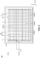
- FIG. 8 is a partial top view illustrating an electronic device 103 according to one embodiment of the present disclosure. It should be noted that some elements may be omitted in FIG. 8 for the sake of brevity.
- the electronic device 103 as shown in FIG. 8 is similar to the electronic device 102 as shown in FIG. 4 .
- the conductive structure 60 of the electronic device 103 may be interdigitated.
- the conductive structure 60 may include a first portion 61 and a second portion 62.
- the first portion 61 may be divided into a section 61-1 and a section 61-2
- the second portion 62 may include at least one first signal line SL1 and at least one second signal line SL2, but it is not limited thereto.
- the first signal lines SL1 and the second signal lines SL2 may be extended along the X-direction as shown in FIG. 8 , but it is not limited thereto.
- the first signal lines SL1 and the second signal lines SL2 may be alternately disposed. That is, the first signal lines SL1 and the second signal lines SL2 may not overlap in the Z-direction, but it is not limited thereto.
- the material of the first signal line SL1 may be the same as or different from the material of the second signal line SL2.
- the first signal line SL1 may be connected to section 61-1 of the first portion 61, and the first signal line SL1 may be electrically connected to the circuit board 71 (or the voltage-signal supply circuit) through section 61-1, but it is not limited thereto.
- the second signal line SL2 may be connected to section 61-2 of the first portion 61, and the second signal line SL2 may be electrically connected to the circuit board 72 (or the voltage-signal supply circuit) through section 61-2, but it is not limited thereto.
- the circuit board 71 and the circuit board 72 may be used for supplying or transmitting the same voltage signal or different voltage signals.
- the circuit board 71 may be used for supplying or transmitting supply voltage (VDD)
- the circuit board 72 may be used for supplying or transmitting supply voltage (VSS) or ground reference voltage, but it is not limited thereto.
- the section 61-1 and the section 61-2 may be electrically insulated from each other.
- the electronic device 103 may further include at least one circuit board 73, and the circuit board 73 may be disposed on the first substrate.
- the conductive pads (not shown) of the circuit board 73 may be electrically connected to conductive pads (not shown, and different from the conductive pads of the first signal pads and the first electrode pads) of the first substrate 11 the as shown in FIG. 8 .
- the conductive pads of the circuit board 73 may be electrically connected to the conductive pads of the first substrate 11 directly, or the conductive pads of the circuit board 73 may be electrically connected to conductive pads of the first substrate 11 through an anisotropic conductive film (ACF).
- ACF anisotropic conductive film
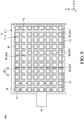
- FIG. 9 is a partial top view illustrating an electronic device 104 according to one embodiment of the present disclosure. It should be noted that some elements may be omitted in FIG. 9 , for the sake of brevity.
- the electronic device 104 as shown in FIG. 9 is similar to the electronic device 102 as shown in FIG. 4 .
- the second portion 62 of the conductive structure 60 may include the signal lines SL extending along the X-direction, and signal lines SL extending along the Y-direction. That is, the signal lines SL of the second portion 62 may form a grid structure (or net structure), but it is not limited thereto.
- the light-emitting (or display) uniformity of the electronic device may be increased by the conductive structure 60.
- the second portion 62 of the conductive structure 60 may include the signal lines SL extending along other directions. In some embodiments, the shape of the second portion 62 of the conductive structure 60 may have other irregular-shaped. In some embodiments, one of the first light-emitting units 41 may be connected and disposed corresponding to at least one of the first signal pads 51 as shown in FIG. 9 . In some embodiments, the number of the first signals pad 51 and/or the positions of the first signals pad 51 connected and disposed corresponding to different first light-emitting units 41 may be the same or different.
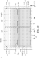
- FIG. 10 is a partial top view illustrating a tiled electronic device 1 according to one embodiment of the present disclosure.
- the tiled electronic device 1 may include a plurality of electronic devices 100'.
- the structure of the electronic devices 100' may be similar to the structure of the electronic devices 100 as shown in FIG. 1 , the structure of the electronic devices 102 as shown in FIG. 2 , the structure of the electronic devices 102' as shown in FIG. 6 , the structure of the electronic devices 103 as shown in FIG. 8 , or the structure of the electronic devices 104 as shown in FIG. 9 , except for the conductive structure 60.
- the conductive structure 60' of the tiled electronic device 1 may be divided into a first portion 61' and a second portion 62', the first portion 61' may be disposed corresponding to (or overlap) the non-operating region (or non-display region), and the second portion 62' may be disposed corresponding to (or overlap) the operating region (or display region) as shown in FIG. 10 .
- the material of the first portion 61' of the conductive structure 60' may be the same as or similar to the material of the first portion 61 of the conductive structure 60
- the material of the second portion 62' of the conductive structure 60' may be the same as or similar to the material of the second portion 62 of the conductive structure 60.
- the material of the first portion 61' of the conductive structure 60' may be the same as or different than the material of the second portion 62' of the conductive structure 60'.
- the first portion 61' of the conductive structure 60' may be disposed corresponding to (or overlap) a tiled seam TG between two substrates as shown in FIG. 10 , and the first portion 61' may be electrically connected with at least one signal line SL and the circuit board 70.
- the first portion 61' may be electrically connected to the circuit board 70 (e.g., the conductive pad 80 of the circuit board 70), and the first portion 61' may transit the voltage signal to the signal line SL (or voltage-signal supply circuit).
- the signal line SL may be disposed corresponding to (or overlap) and be electrically connected to the signal pads (e.g., the first signal pads 51 or second signal pads 52 mentioned above) in different substrates, and the voltage signal may be transmitted to the light-emitting units (e.g., the first light-emitting units 41 or second light-emitting units 42 mentioned above) in different substrates through the signal line SL of the second portion 62', but it is not limited thereto. Due to the conductive structure 60', the transmission efficiency of the voltage signal may be enhanced, or the number of the circuit boards 70 (or the number of the voltage-signal supply circuit) may be reduced.
- tiled electronic device may need to separately set and electrically connect to individual circuit boards between different substrates, and the tiled seam may be lager because the circuit boards need to occupy some spaces of the substrates.
- the electronic device (or the tiled electronic device) of the embodiments according to the present disclosure may deal with the issues.
- a protective material (referring to protective layer CL), a shielding material, other suitable materials or a combination thereof may be disposed (or coated) on the conductive structure 60' (or the conductive structure 60).
- the shielding material may be used for shielding the tiled seam TG between the substrates, and the protective material may be used for reducing collisions or increasing the yield of the electronic devices.
Landscapes
- Engineering & Computer Science (AREA)
- Microelectronics & Electronic Packaging (AREA)
- Electroluminescent Light Sources (AREA)
Abstract
An electronic device includes a first substrate, a first conductive layer, a plurality of first electrode pads, a plurality of first light-emitting units, a plurality of first signal pads and a conductive structure. The first conductive layer is disposed on the first substrate. The first electrode pads are disposed on the first conductive layer. The first light-emitting units overlap and are disposed on the first electrode pads. The first light-emitting units are electrically connected to the first electrode pads respectively. The first signal pads are disposed on the first conductive layer and electrically connected to the first conductive layer. The conductive structure is disposed on the first signal pads, and at least two of the first signal pads are electrically connected to each other through the conductive structure.
Description
- This application claims the benefit of
U.S. Provisional Application No. 62/680,665, filed June 5, 2018 201910104660.7, filed February 1, 2019 - Embodiments of the present disclosure relate to an electronic device, and in particular they relate to an electronic device including a conductive structure.
- As technology advances, some electronic devices are designed to have a larger size, high resolution, thin or narrow frame, etc., and the tiled electronic devices are designed to have such characteristics. There are still many aspects of current electronic devices that need improvement. Therefore, how to satisfy the above characteristics has become a subject.
- It is an object of the present disclosure to provide an electronic device that may deal with the above issues and that enables in particular an even signal transmission with a low-cost configuration with reduced space requirements. In particular the present disclosure is to provide an electronic device designed to have a larger size, high resolution, thin or narrow frame, for example a tiled electronic device.
- These problems are reduced by an electronic device as claimed in
claim 1. Further advantageous embodiments are the subject-matter of the dependent claims. - In accordance with some embodiments of the present disclosure, an electronic device includes a first substrate, a first conductive layer, a plurality of first electrode pads, a plurality of first light-emitting units, a plurality of first signal pads and a conductive structure. The first conductive layer is disposed on the first substrate. The first electrode pads are disposed on the first conductive layer. The first light-emitting units overlap and are disposed on the first electrode pads. The first light-emitting units are electrically connected to the first electrode pads respectively. The first signal pads are disposed on the first conductive layer and electrically connected to the first conductive layer. The conductive structure is disposed on the first signal pads, and at least two of the first signal pads are electrically connected to each other through the conductive structure.
- Aspects of the embodiments of the present disclosure can be understood from the following detailed description when read with the accompanying figures. It should be noted that, in accordance with the standard practice in the industry, various features are not drawn to scale. In fact, the dimensions of the various features may be arbitrarily increased or reduced for clarity of discussion.
-
FIG. 1 is a partial top view illustrating an electronic device according to one embodiment of the present disclosure. -
FIG. 2 is a partial top view illustrating a tiled electronic device according to one embodiment of the present disclosure. -
FIG. 3 is a partial cross-sectional view illustrating the tiledelectronic device 101 along line A-A' and line B-B' inFIG. 1 . -
FIG. 4 is a partial top view illustrating an electronic device according to another embodiment of the present disclosure. -
FIG. 5 is a partial cross-sectional view illustrating the electronic device along line C-C' inFIG. 4 . -
FIG. 6 is a partial top view illustrating an electronic device according to another embodiment of the present disclosure. -
FIG. 7 is a partial cross-sectional view illustrating the electronic device along line C1-C1' inFIG. 6 . -
FIG. 8 is a partial top view illustrating an electronic device according to one embodiment of the present disclosure. -
FIG. 9 is a partial top view illustrating an electronic device according to one embodiment of the present disclosure. -
FIG. 10 is a partial top view illustrating a tiled electronic device according to one embodiment of the present disclosure. - The following disclosure provides many different embodiments, or examples, for implementing different features of the subject matter provided. Specific examples of components and arrangements are described below to simplify the present disclosure. These are, of course, merely examples and are not intended to be limiting. For example, a first feature is disposed on (or formed on) a second feature in the description that follows may include embodiments in which the first feature and second feature are disposed (or formed) in direct contact, and may also include embodiments in which additional features may be disposed (or formed) between the first feature and second feature, so that the first feature and second feature may not be in direct contact.
- It should be understood that additional steps may be implemented before, during, or after the illustrated methods, and some steps might be replaced or omitted in other embodiments of the illustrated methods.
- Furthermore, spatially relative terms, such as "beneath," "below," "lower," "on," "above," "upper" and the like, may be used herein for ease of description to describe one element or feature's relationship to other elements or features as illustrated in the figures. The spatially relative terms are intended to encompass different orientations of the device in use or operation in addition to the orientation depicted in the figures. The apparatus may be otherwise oriented (rotated 45 degrees or at other orientations) and the spatially relative descriptors used herein may likewise be interpreted accordingly.
- In the present disclosure, the terms "about" and "substantially" typically mean +/-20% of the stated value, more typically +/-10% of the stated value, more typically +/-5% of the stated value, more typically +/-3% of the stated value, more typically +/-2% of the stated value, more typically +/-1% of the stated value and even more typically +/-0.5% of the stated value. The stated value of the present disclosure is an approximate value. That is, when there is no specific description of the terms "about" and "substantially", the stated value includes the meaning of "about" or "substantially".
- It should be understood that, although the terms "first," "second," "third," etc. can be used herein to describe various elements, components, regions, layers and/or sections, these elements, components, regions, layers and/or sections should not be limited through these terms. These terms are only used to distinguish one element, component, region, layer or section from another region, layer or section. Thus, a first element, component, region, layer or section discussed below could be termed a second element, component, region, layer or section without departing from the teachings of the present disclosure.
- Unless otherwise defined, all terms (including technical and scientific terms) used herein have the same meaning as commonly understood through one of ordinary skill in the art to which this disclosure belongs. It should be understood that terms such as those defined in commonly used dictionaries should be interpreted as having a meaning that is consistent with their meaning in the context of the relevant art and will not be interpreted in an idealized or overly formal sense unless expressly so defined in the embodiments of the present disclosure.
- Further, the elements in the drawings are merely illustrative, and the dimensions (including length, width, or height) of the elements should not be limited in the drawings. Furthermore, the electronic device described in the present disclosure may include a display device, a light-emitting device, a detecting device, a touch device, or other suitable device, but the disclosed embodiments are not limited thereto.
-
FIG. 1 is a partial top view illustrating anelectronic device 100 according to one embodiment of the present disclosure.FIG. 2 is a partial top view illustrating a tiledelectronic device 101 according to one embodiment of the present disclosure.FIG. 3 is a partial cross-sectional view illustrating the tiledelectronic device 101 along line A-A' and line B-B' inFIG. 1 . In the embodiment as shown inFIG.1 , theelectronic device 100 may include a substrate, and in the embodiment as shown inFIG.2 , the tiledelectronic device 101 may include a plurality of substrates. It should be noted that, the corresponding positions or the materials of the elements (or layers) on the substrate of theelectronic device 100 may be the same as or be similar to the corresponding elements (or layers) disposed on the plurality of substrates of the tiledelectronic device 101. The elements (or layers) mentioned above may include conductive layers, electrode pads, light-emitting units, signal pads or other suitable elements (or layers), which may refer to the following embodiments (as shown inFIG. 1 to FIG. 3 ) in more detail. Therefore, the cross-sectional view of theelectronic device 100 may also refer to the cross-sectional view as shown inFIG. 3 . - Referring to
FIG. 1 andFIG. 3 , theelectronic device 100 includes afirst substrate 11, a firstconductive layer 21, a plurality offirst electrode pads 31, a plurality of first light-emitting units 41, a plurality offirst signal pads 51 and aconductive structure 60. The firstconductive layer 21 may be electrically connected to the plurality offirst electrode pads 31 and the plurality offirst signal pads 51, respectively. For example, thefirst substrate 11 may be an array substrate, and the firstconductive layer 21 may be disposed (or formed) on thefirst substrate 11. In some embodiments, the firstconductive layer 21 may be used as the conductive line for transmitting voltage signals. The material of the firstconductive layer 21 may include metals (e.g., copper, molybdenum, aluminum, tungsten, gold, chromium, nickel, platinum, titanium), alloys (e.g., alloys of the above metals), transparent conductive materials, other suitable conductive materials, or a combination thereof, but it is not limited thereto. The transparent conductive materials may include indium tin oxide (ITO), tin oxide (TO), indium zinc oxide (IZO), indium gallium zinc oxide (IGZO), antimony-doped tin oxide (ATO), aluminium-doped zinc oxide (AZO), but it is not limited thereto. The firstconductive layer 21 may include a single-layer material, a multi-layer material or a composite material. In some embodiments, thefirst electrode pads 31 are disposed on the firstconductive layer 21, the first light-emittingunits 41 overlap and are disposed on thefirst electrode pads 31, and the first light-emittingunits 41 are electrically connected to thefirst electrode pads 31, respectively. In more detail, the cathode (and/or anode) of the first light-emittingunit 41 may be electrically connected to the firstconductive layer 21 through thefirst electrode pads 31. That is, thefirst electrode pads 31 may be used as the pads of the first light-emittingunits 41. In some embodiments, the first light-emittingunits 41 may include light-emitting diodes (LED), micro LED, mini LED, quantum dot light-emitting diodes (QLED/QDLED), quantum dots or other suitable components, but it is not limited thereto. In some embodiments, the first light-emittingunits 41 may include organic light-emitting diodes (OLED), but it is not limited thereto. - In some embodiments, the
first signal pads 51 are disposed on the firstconductive layer 21 and electrically connected to the firstconductive layer 21, theconductive structure 60 is disposed on thefirst signal pads 51, and at least two of thefirst signal pads 51 are electrically connected to each other through theconductive structure 60 as shown inFIG. 3 . For example, thefirst signal pads 51 are disposed between theconductive structure 60 and the firstconductive layer 21 in the Z-direction (i.e., the normal direction of the first substrate 11), and theconductive structure 60 is electrically connected to the firstconductive layer 21 through thefirst signal pads 51 as shown inFIG. 1 andFIG. 3 . In some embodiments, theconductive structure 60 may overlap at least part of thefirst signal pads 51 in the Z-direction. - In some embodiments, the
conductive structure 60 is electrically connected to thecircuit board 70 as shown inFIG. 1 or voltage-signal supply circuits (not shown). Thecircuit board 70 may include a flexible printed circuit (FPC), a chip on film (COF) or a printed circuit board (PCB), but it is not limited thereto. In some embodiments, thecircuit board 70 may be electrically connected to the firstconductive layer 21 through a conductive pad 80 (seeFIG. 3 ). In more detail, thecircuit board 70 is disposed on thefirst substrate 11, at least one voltage signal transmitted through (or supplied from) thecircuit board 70 may be transmitted to the firstconductive layer 21 through theconductive structure 60, and the voltage signal may be transmitted to the first light-emittingunits 41 through the firstconductive layer 21. The first light-emittingunits 41 may modulate the light to be emitted or the brightness of the light according to the received voltage signal, but the present disclosure is not limited thereto. The voltage signal mentioned above may include a supply voltage (e.g., VDD, VSS), a bias voltage, a reset voltage, a ground voltage (GND), or another suitable voltage signal, but it is not limited thereto. - In some embodiments, the
first signal pads 51 may be used as power pads, but it is not limited thereto. In some embodiments, the material of thefirst electrode pads 31 may be the same as the material of thesignal pads 51, or the material of thefirst electrode pads 31 may be different from the material of thesignal pads 51. In some embodiments, the material of the first electrode pads 31 (or the material of the signal pads 51) may include nickel, copper, gold, tin, silver, other suitable conductive materials, alloys of the above metals or a combination thereof, but it is not limited thereto. It should be noted that the connecting relationship between thefirst signal pads 51 and the firstconductive layer 21 is not limited to that as shown inFIG. 3 . Other suitable conductive materials may be disposed between thefirst signal pads 51 and the firstconductive layer 21. - In some embodiments, the voltage signals transmitted through (or supplied from) the
circuit board 70 may be transmitted to the light-emitting units (e.g., the first light-emitting units 41) by theconductive structure 60 with low impedance, which can enhance the transmission efficiency of the voltage signal or reduce the number ofcircuit boards 70. For example, the impedance of theconductive structure 60 may be lowered by increasing the thickness T of theconductive layer 60 as shown inFIG. 3 , or by using a low-impedance material (e.g., gold, silver, copper) in theconductive layer 60, but the present disclosure is not limited thereto. In some embodiments, the thickness T of theconductive layer 60 may be greater than or equal to the thickness T2 of the firstconductive layer 21 as shown inFIG. 3 , but it is not limited thereto. The thickness T of theconductive layer 60 may be defined by a maximum thickness of theconductive layer 60 in the Z-direction, and the thickness T2 of the firstconductive layer 21 may be defined by a minimum thickness of the firstconductive layer 21 in the Z-direction. The detailed measurement method of the above thicknesses will be described later. - In some embodiments, the
first substrate 11 may be divided into a first region 11-1 and a second region 11-2, and the first region 11-1 may be adjacent to (or surround) the second region 11-2 as show inFIG. 1 . The first region 11-1 may be a non-operating region (or non-display region), while the second region 11-2 may be an operating region (or display region). In some embodiments, the outermost first light-emitting units may respectively has at least one side edge closest to the edge of thefirst substrate 11 as shown inFIG. 1 . The connected lines (such as the dashed-lines shown inFIG. 1 ) of these side edges (or the extension lines of the side edges) may form a second region 11-2 of thefirst substrate 11, and a region other than the second region 11-2 is the first region 11-1 of thefirst substrate 11. For example, the first light-emittingunits 41 may include the light-emitting diodes, micro LED, mini LED or quantum dot light-emitting diodes, the profile of the first light-emittingunit 41 may be defined by the boundary of the first light-emittingunit 41 projecting on thefirst substrate 11 in the Z-direction, but it is not limited thereto, and the side edges closest to the edge of thefirst substrate 11 may be obtained from the profile. Or, the profile of the first light-emittingunits 41 may be defined by the boundary of the uppermost layers (or elements) included in the first light-emittingunits 41 projecting on thefirst substrate 11 in the Z-direction, but it is not limited thereto, and the side edges closest to the edge of thefirst substrate 11 may be obtained from such profile. In some embodiments, one of the first light-emittingunits 41 may include a cathode electrode, an anode electrode or a light-emitting layer, but it is not limited thereto. - In some embodiments (not shown), the first light-emitting
units 41 include organic light-emitting diodes, and the boundary of the first light-emittingunits 41 may be defined by a pixel defining layer (PDL), but it is not limited thereto. For example, the pixel defining layer (now shown) may be disposed on thefirst substrate 11, and the pixel defining layer may have a plurality of openings. The first light-emittingunits 41 may respectively be disposed corresponding to or overlap the openings of the pixel defining layer. The projecting area of the openings of the pixel defining layer on thefirst substrate 11 may be defined as the profile of the first light-emittingunits 41, but it is not limited thereto. - As shown in
FIG. 1 , the first light-emittingunits 41 may be disposed corresponding to (or overlap) the second region 11-2 of thefirst substrate 11. That is, the first light-emittingunits 41 may be disposed in the second region 11-2. Theconductive structure 60 may be disposed corresponding to (or overlap) the first region 11-1 of thefirst substrate 11. That is, theconductive structure 60 may be disposed in the first region 11-1, but it is not limited thereto. - In some embodiments, the
conductive structure 60 may have at least one openings O, and the openings O may be disposed corresponding to (or overlap) the second region 11-2 as shown inFIG. 1 ; or the openings O may overlap at least one of the first light-emittingunits 41. In some embodiments, at least part of theconductive structure 60 may overlap at least one of the first light-emittingunits 41. - Referring to
FIG. 2 andFIG. 3 , theelectronic device 101 may be a tiled electronic device. Theelectronic device 101 includes afirst substrate 11, a firstconductive layer 21, a plurality offirst electrode pads 31, a plurality of first light-emittingunits 41, a plurality offirst signal pads 51 and aconductive structure 60. Moreover, theelectronic device 101 further includes asecond substrate 12, a secondconductive layer 22, a plurality ofsecond electrode pads 32, a plurality of second light-emittingunits 42 and a plurality ofsecond signal pads 52. Thesecond substrate 12 may be an array substrate. The secondconductive layer 22 may be disposed (or formed) on thesecond substrate 12, and the secondconductive layer 22 may be electrically connected to the plurality ofsecond electrode pads 32 and the plurality ofsecond signal pads 52. The material of the secondconductive layer 22, the material of thesecond electrode pads 32, and/or the material of thesecond signal pads 52 may be the same as or different from the material of the firstconductive layer 21, the material of thefirst electrode pads 31, and/or the material of thefirst signal pads 51, respectively. - In some embodiments (
FIG. 3 ), thesecond electrode pads 32 are disposed on the secondconductive layer 22, the second light-emittingunits 42 may overlap (or be disposed on) thesecond electrode pads 32, and the second light-emittingunits 42 are electrically connected to thesecond electrode pads 32 respectively. Thesecond electrode pads 32 may be used as the pads of the second light-emittingunits 42, and the second light-emittingunits 42 may be electrically connected to the secondconductive layer 22 through thesecond electrode pads 32. - In some embodiments, the
second signal pads 52 are disposed on the secondconductive layer 22, and thesecond signal pads 52 are electrically connected to the secondconductive layer 22, theconductive structure 60 is disposed on thesecond signal pads 52, and at least two of thesecond signal pads 52 are electrically connected to each other through theconductive structure 60 as shown inFIG. 3 . For example, thesecond signal pads 52 are disposed between theconductive structure 60 and the secondconductive layer 22 in the Z-direction (i.e., the normal direction of the second substrate 12). In some embodiments, theconductive structure 60 is electrically connected to the secondconductive layer 22 through thesecond signal pads 52 as shown inFIG. 2 andFIG. 3 . In some embodiments, theconductive structure 60 may overlap at least part of thesecond signal pads 52 in the Z-direction. - Moreover, similar to the
first substrate 11, thesecond substrate 12 may be divided into a first region 12-1 and a second region 12-2, and the first region 12-1 may be adjacent to (or surround) the second region 12-2. The first region 12-1 of thesecond substrate 12 may be a non-operating region (or non-display region), the second region 12-2 of thesecond substrate 12 may be an operating region (or display region). The definition of the first region 12-1 of thesecond substrate 12 and the definition of the second region 12-2 of thesecond substrate 12 may be similar to the definition of the first region 11-1 of thefirst substrate 11 and the definition of the second region 11-2 of thefirst substrate 11, which will not be repeated here. As shown inFIG. 2 , the second light-emittingunits 42 may be disposed corresponding to (or overlap) the second region 12-2 of thesecond substrate 12. That is, the second light-emittingunits 42 may be disposed in the second region 12-2. Theconductive structure 60 may be disposed corresponding to (or overlap) the first region 12-1 of thesecond substrate 12. That is, theconductive structure 60 may be disposed in the first region 12-1, but it is not limited thereto. In some embodiments, thesecond signal pads 52 may be disposed corresponding to (or overlap) the first region 12-1. That is, thesecond signal pads 52 may be disposed in the first region 12-1, but it is not limited thereto. - In some embodiments, the
conductive structure 60 may have at least one openings O, and the openings O may be disposed corresponding to (or overlap) the second region 11-2 and/or the second region 12-2 as shown inFIG. 2 ; or the openings O may overlap at least one of the first light-emittingunits 41 and/or at least one of the second light-emittingunits 42. In some embodiments, at least one portion of theconductive structure 60 may overlap at least one of the second light-emittingunits 42. - In some embodiments, the
circuit board 70 may be electrically connected to at least one of thefirst signal pads 51 and at least one of thesecond signal pads 52 throughconductive structure 60. In more detail, at least one voltage signal transmitted through (or supplied from) thecircuit board 70 may be transmitted to the firstconductive layer 21 and/or the secondconductive layer 22 through theconductive structure 60, and the voltage signals may be transmitted to the first light-emittingunits 41 through the firstconductive layer 21, and the voltage signals may be transmitted to the second light-emittingunits 42 through the secondconductive layer 22, but it is not limited thereto. Thesecond signal pads 52 may be used to connect theconductive structure 60 to the secondconductive layer 22. In some embodiments, thesecond signal pads 52 may be used as power pads, but it is not limited thereto. - In some embodiments, the connecting relationships between various elements (or layers) or the materials of various elements (or layers) disposed on the
second substrate 12 may be the same as or similar to those disposed on thefirst substrate 11, except for the conductive structure. The elements (or layers) mentioned above may include the conductive layer, the electrode pads, the light-emitting units, the signal pads or other suitable elements (or layers). - It should be noted that, the
electronic device 101 having four substrates is used as an example, but the present disclosure is not limited thereto. The electronic device may be a tiled electronic device having more or fewer substrates. The number and arrangement of the substrates (including thefirst substrate 11 or the second substrate 12), the light-emitting units (including the first light-emittingunits 41 or the second light-emitting units 42), the signal pads (including thefirst signal pads 51 or the second signal pads 52) or other elements as shown in the figures of the present disclosure are examples only, and the present disclosure is not limited thereto. The substrates (including thefirst substrate 11 or the second substrate 12) as shown in the figures of the present disclosure are illustrated to be rectangular, but those are examples. In some embodiments, the shape of substrates (including thefirst substrate 11 or the second substrate 12) may include curved, polygonal, obtuse, acute or irregular shapes. Furthermore, the number of thecircuit boards 70, the position of thecircuit boards 70 or the way for electrically connecting thecircuit boards 70 and theconductive structure 60 are not limited to the embodiments as shown inFIG. 1 andFIG. 2 . In some embodiments, thecircuit boards 70 may be in direct contact with theconductive structure 60, and thecircuit boards 70 may be electrically connected to theconductive structure 60; or thecircuit boards 70 may be electrically connected to theconductive structure 60 by other conductive elements (e.g., the circuit structure LS), which will be described in followingFIG. 6 andFIG. 7 . - In some embodiments, the
conductive structure 60 may be manufactured by inkjet printing or net technology, and may be disposed on thefirst signal pads 51 and thesecond signal pads 52 by compression, welding or laser heating, but the present disclosure is not limited thereto. - In some embodiments, the electronic device 101 (or the electronic device 100) may include a protective layer CL, and the protective layer CL may be disposed on the
conductive structure 60 as shown inFIG. 3 . In some embodiments, the protective layer CL may cover theconductive structure 60, and not overlap or cover the light-emitting units (such as the first light-emittingunits 41 and the second light-emitting units 42), but it is not limited thereto. In some embodiments, the protective layer CL may cover a portion of an insulating layer IL, and the insulating layer IL may be disposed between the firstconductive layer 21 and the first light-emittingunits 41. In some embodiments, the insulating layer IL may be disposed between the secondconductive layer 22 and the second light-emittingunits 42, but it is not limited thereto. In some embodiments, the material of the protective layer CL may include an absorption material, a light-shielding material, a material having buffering feature, a material having protective feature or a combination thereof, but it is not limited thereto. In some embodiments, the material of the protective layer CL may be water-proof, antistatic or antifouling. In some embodiments, the protective layer CL may include a single-layer material, a multi-layer material or a composite material. In some embodiments, the thickness T4 of the protective layer CL may be less than or equal to the thickness T of theconductive structure 60. In other embodiments, the thickness T4 of the protective layer CL may be greater than or equal to the thickness T of theconductive structure 60. The thickness T4 of the protective layer CL may be defined by a minimum thickness of the protective layer CL in the Z-direction. In some embodiments, the material of the protective layer CL may include a transparent material, and at least part of the protective layer CL may overlap or not overlap the light-emitting units. -
FIG. 4 is a partial top view illustrating anelectronic device 102 according to another embodiment of the present disclosure.FIG. 5 is a partial cross-sectional view illustrating theelectronic device 102 along line C-C' inFIG. 4 . The embodiment as shown inFIG. 4 is similar to the embodiment as shown inFIG. 1 . Thefirst substrate 11 may be divided into a first region 11-1 and a second region 11-2, and the plurality of first light-emittingunits 41 may be disposed corresponding to the second region 11-2. The differences between the embodiment as shown inFIG. 4 and the embodiment as shown inFIG. 1 is that theconductive structure 60 of theelectronic device 102 may be disposed corresponding to (or overlap) the first region 11-1 and the second region 11-2. That is, theconductive structure 60 may be disposed in first region 11-1 and the second region 11-2. - In some embodiments, the
conductive structure 60 may be divided into afirst portion 61 and asecond portion 62 as shown inFIG. 4 andFIG. 5 . Thefirst portion 61 may be disposed corresponding to (or overlap) the first region 11-1. That is, thefirst portion 61 may be disposed in the first region 11-1. Thesecond portion 62 may be disposed corresponding to (or overlap) the second region 11-2. That is, thesecond portion 62 may be disposed in the second region 11-2. - In some embodiments, the
second portion 62 of theconductive structure 60 may include at least one signal line SL. InFIG. 4 , the signal lines SL may extend along the X-direction, but it is not limited thereto. In other embodiments (e.g., the embodiment as shown in followingFIG. 9 ), the signal lines SL may extend along the Y-direction or other directions. In some embodiments, the material of the signal line SL may include a material having low impedance, but it is not limited thereto. In some embodiments, the material of the signal line SL may include metals (e.g., gold, silver, copper, etc.), alloys or other suitable materials, but it is not limited thereto. In some embodiments, the material of the signal line SL may include a single-layer material, a multi-layer material or a composite material. - In some embodiments, the thickness T1 of the signal line SL may be greater than or equal to the thickness T2 of the first
conductive layer 21 as shown inFIG. 5 . In some embodiments, the thickness T of thefirst portion 61 of theconductive structure 60 may be the same as or different from the thickness T1 of the signal line SL. In some embodiments, the material of thefirst portion 61 of theconductive structure 60 may be the same as or different from the material of the second portion 62 (e.g., the signal lines SL) of theconductive structure 60. In some embodiments, the material of thefirst portion 61 of theconductive structure 60 may be the same as the material of the signal line SL, and the thickness T of thefirst portion 61 of theconductive structure 60 may be substantially the same as the thickness T1 of the signal line SL as shown inFIG. 5 , but it is not limited thereto. In some embodiments, thefirst portion 61 of theconductive structure 60 and the signal lines SL may be manufactured in the same process. In some embodiments, thefirst portion 61 of theconductive structure 60 may be connected to or contact with thesecond portion 62 of theconductive structure 60. - In some embodiments, the width W of the signal line SL of the
second portion 62 of theconductive structure 60 may be less than or equal to the gap S between two adjacent first light-emittingunits 41 as shown inFIG. 5 . The width W may be defined by a maximum width of the signal line SL along a direction perpendicular to an extending direction of the signal line SL. For example, the signal lines SL extend along the X-direction as shown inFIG. 4 andFIG. 5 , so the width W may be defined by the maximum width of the signal line SL in the Y-direction, wherein Y-direction may be perpendicular to X-direction and Z-direction. The gap S may be defined by a minimum gap between two adjacent ones of first light-emittingunits 41 in the direction perpendicular to the extending direction of the signal line SL. For example, the signal lines SL extend along the X-direction as shown inFIG. 4 andFIG. 5 , and the gap S may be defined by the minimum gap between two adjacent ones of first light-emittingunits 41 in the Y-direction. - In some embodiments, the ratio of the width W of the signal line SL of the
second portion 62 of theconductive structure 60 to the gap S between two adjacent first light-emitting units 41 (i.e., W/S) may be between 0.05 and 0.95 (0.05 ≦ W/S ≦ 0.95). In some embodiments, W/S may be between 0.05 and 0.4 (0.05 ≦ W/S ≦ 0.4), or between 0.4 and 0.7 (0.4 ≦ W/S ≦ 0.7), or between 0.7 and 0.95 (0.7 ≦ W/S ≦ 0.95). - It should be noted that, if the width W of the signal line SL of the
second portion 62 of theconductive structure 60 may be narrow, the impedance may be higher, and the voltage signals cannot be uniformly transmitted to the light-emitting units. Moreover, if the width W of the signal line SL of thesecond portion 62 is greater than the gap S, the lights emitted from the first light-emitting units 41 (and/or the second light-emitting units 42) may be shielded, which may influence the brightness of the lights. Therefore, if W/S is in the range mentioned above, which can increase the uniformly of voltage signals transmitted to the light-emitting units, or the influence of the brightness of the lights may be reduced. - It should be noted that the width W and/or the gap S may be measured using optical microscopy (OM), but it is not limited thereto. The OM image may include at least two first light-emitting
units 41 and one signal line SL, the maximum width of the signal line SL in the image may be measured to obtain the width W, and the minimum gap between two adjacent ones of the first light-emittingunits 41 in the image may be measured to obtain the gap S, but it is not limited thereto. The width W and the gap S may be obtained by observing local cross-sectional view (e.g., the C-C' cross-sectional view inFIG. 5 , but it is not limited thereto) using a scanning electron microscope (SEM). In the local cross-sectional view, the maximum width of the signal line SL may be measured to obtain the width W, and the minimum gap between two adjacent ones of the first light-emittingunits 41 may be measured to obtain the gap S, but it is not limited thereto. - As shown in
FIG. 5 , the signal line SL of thesecond portion 62 of theconductive structure 60 may have a thickness T1, and the firstconductive layer 21 may have a thickness T2. In some embodiments, the ratio of thickness T1 to thickness T2 may be between 10 and 300 (10 ≦ T1/T2 ≦ 300), but it is not limited thereto. In some embodiments, the ratio of thickness T1 to thickness T2 may be between 10 and 200 (10 ≦ T1/T2 ≦ 200). In some embodiments, the ratio of thickness T1 to thickness T2 may be between 10 and 100 (10 ≦ T1/T2 ≦ 100). In some embodiments, the thickness T1 may be greater than or equal to the thickness T2. The thickness T1 may be defined by a maximum thickness of the signal line SL in the Z-direction, and the thickness T2 may be defined by a minimum thickness of the firstconductive layer 21 in the Z-direction. - In some embodiments, the thickness T2 of the first
conductive layer 21 may be between 1 µm and 10 µm (1 µm ≦ T2 ≦ 10 µm). In some embodiments, the thickness T2 of the firstconductive layer 21 may be between 1 µm and 2µm 1 µm ≦ T2 ≦ 2 µm), or between 5 µm and 10 µm (5 µm ≦ T2 ≦ 10 µm). The thickness T1 of the signal line SL may be between 100 µm and 300 µm (100 µm ≦ T1 ≦ 300 µm). In some embodiments, the thickness T1 of the signal line SL may be between 100 µm and 200 µm (100 µm ≦ T1 ≦ 200 µm), or between 200 µm and 300 µm (200 µm ≦ T1 ≦ 300 µm). In some embodiments, one of thefirst signal pads 51 may have a thickness T3 as shown inFIG. 5 , and the ratio of thickness T1 of the signal line SL to thickness T3 of one of thefirst signal pads 51 may be between 0.05 and 100 (0.05 ≦ T1/T3 ≦ 100), but it is not limited thereto. In some embodiments, the ratio of thickness T1 to thickness T3 may be between 0.5 and 50 (0.5 ≦ T1/T3 ≦ 50). It should be noted that the thickness of the above elements may be obtained by observing a local cross-sectional view (e.g., the C-C' cross-sectional view inFIG. 5 , but it is not limited thereto) using a scanning electron microscope, and the thickness of the corresponding elements (or layers) may be measured in a local cross-sectional view, or they may be measured by another suitable measuring method. -
FIG. 6 is a partial top view illustrating an electronic device 102' according to another embodiment of the present disclosure.FIG. 7 is a partial cross-sectional view illustrating the electronic device 102' along line C1-C1' inFIG. 6 . The embodiment as shown inFIG. 6 is similar to the embodiment as shown inFIG. 4 . The differences between the embodiment as shown inFIG. 6 and the embodiment as shown inFIG. 4 is that the electronic device 102' may further include a circuit structure LS, and the circuit structure LS may be disposed corresponding to (or overlap) the first region 11-1 of thefirst substrate 11. In some embodiments, the circuit structure LS may be disposed under thefirst portion 61 of theconductive structure 60 as shown inFIG. 7 , and thefirst portion 61 may be electrically connected to theconductive pad 80 of thecircuit board 70 through the circuit structure LS, but it is not limited thereto. In some embodiments, the circuit structure LS may be disposed under thefirst portion 61 of theconductive structure 60, and theconductive structure 60 may be electrically connected to a voltage-signal supply circuit (not shown) through the circuit structure LS, but it is not limited thereto. In some embodiments, the circuit structure LS may include a composite-layer structure, which may include at least one dielectric layer DL and at least one circuit layer LL, the circuit layer LL may be electrically connected to theconductive pad 80 of thecircuit board 70 as shown inFIG. 7 , but it is not limited thereto. -
FIG. 8 is a partial top view illustrating anelectronic device 103 according to one embodiment of the present disclosure. It should be noted that some elements may be omitted inFIG. 8 for the sake of brevity. Theelectronic device 103 as shown inFIG. 8 is similar to theelectronic device 102 as shown inFIG. 4 . One of the differences between these electronic devices is that theconductive structure 60 of theelectronic device 103 may be interdigitated. For example, theconductive structure 60 may include afirst portion 61 and asecond portion 62. Thefirst portion 61 may be divided into a section 61-1 and a section 61-2, and thesecond portion 62 may include at least one first signal line SL1 and at least one second signal line SL2, but it is not limited thereto. - In some embodiments, the first signal lines SL1 and the second signal lines SL2 may be extended along the X-direction as shown in
FIG. 8 , but it is not limited thereto. In some embodiments, the first signal lines SL1 and the second signal lines SL2 may be alternately disposed. That is, the first signal lines SL1 and the second signal lines SL2 may not overlap in the Z-direction, but it is not limited thereto. In some embodiments, the material of the first signal line SL1 may be the same as or different from the material of the second signal line SL2. In some embodiments, the first signal line SL1 may be connected to section 61-1 of thefirst portion 61, and the first signal line SL1 may be electrically connected to the circuit board 71 (or the voltage-signal supply circuit) through section 61-1, but it is not limited thereto. In some embodiments, the second signal line SL2 may be connected to section 61-2 of thefirst portion 61, and the second signal line SL2 may be electrically connected to the circuit board 72 (or the voltage-signal supply circuit) through section 61-2, but it is not limited thereto. - In some embodiments, the
circuit board 71 and thecircuit board 72 may be used for supplying or transmitting the same voltage signal or different voltage signals. For example, thecircuit board 71 may be used for supplying or transmitting supply voltage (VDD), and thecircuit board 72 may be used for supplying or transmitting supply voltage (VSS) or ground reference voltage, but it is not limited thereto. In some embodiment, the section 61-1 and the section 61-2 may be electrically insulated from each other. - In some embodiments, the
electronic device 103 may further include at least onecircuit board 73, and thecircuit board 73 may be disposed on the first substrate. In more detail, the conductive pads (not shown) of thecircuit board 73 may be electrically connected to conductive pads (not shown, and different from the conductive pads of the first signal pads and the first electrode pads) of thefirst substrate 11 the as shown inFIG. 8 . The conductive pads of thecircuit board 73 may be electrically connected to the conductive pads of thefirst substrate 11 directly, or the conductive pads of thecircuit board 73 may be electrically connected to conductive pads of thefirst substrate 11 through an anisotropic conductive film (ACF). -
FIG. 9 is a partial top view illustrating anelectronic device 104 according to one embodiment of the present disclosure. It should be noted that some elements may be omitted inFIG. 9 , for the sake of brevity. Theelectronic device 104 as shown inFIG. 9 is similar to theelectronic device 102 as shown inFIG. 4 . One of the differences between these electronic devices is that thesecond portion 62 of theconductive structure 60 may include the signal lines SL extending along the X-direction, and signal lines SL extending along the Y-direction. That is, the signal lines SL of thesecond portion 62 may form a grid structure (or net structure), but it is not limited thereto. The light-emitting (or display) uniformity of the electronic device may be increased by theconductive structure 60. In some embodiments, thesecond portion 62 of theconductive structure 60 may include the signal lines SL extending along other directions. In some embodiments, the shape of thesecond portion 62 of theconductive structure 60 may have other irregular-shaped. In some embodiments, one of the first light-emittingunits 41 may be connected and disposed corresponding to at least one of thefirst signal pads 51 as shown inFIG. 9 . In some embodiments, the number of thefirst signals pad 51 and/or the positions of thefirst signals pad 51 connected and disposed corresponding to different first light-emittingunits 41 may be the same or different. -
FIG. 10 is a partial top view illustrating a tiledelectronic device 1 according to one embodiment of the present disclosure. As shown inFIG. 1 , the tiledelectronic device 1 may include a plurality of electronic devices 100'. For example, the structure of the electronic devices 100' may be similar to the structure of theelectronic devices 100 as shown inFIG. 1 , the structure of theelectronic devices 102 as shown inFIG. 2 , the structure of the electronic devices 102' as shown inFIG. 6 , the structure of theelectronic devices 103 as shown inFIG. 8 , or the structure of theelectronic devices 104 as shown inFIG. 9 , except for theconductive structure 60. - In some embodiments, the conductive structure 60' of the tiled
electronic device 1 may be divided into a first portion 61' and a second portion 62', the first portion 61' may be disposed corresponding to (or overlap) the non-operating region (or non-display region), and the second portion 62' may be disposed corresponding to (or overlap) the operating region (or display region) as shown inFIG. 10 . In some embodiments, the material of the first portion 61' of the conductive structure 60' may be the same as or similar to the material of thefirst portion 61 of theconductive structure 60, and the material of the second portion 62' of the conductive structure 60' may be the same as or similar to the material of thesecond portion 62 of theconductive structure 60. In this embodiment, the material of the first portion 61' of the conductive structure 60' may be the same as or different than the material of the second portion 62' of the conductive structure 60'. - In some embodiments, the first portion 61' of the conductive structure 60' may be disposed corresponding to (or overlap) a tiled seam TG between two substrates as shown in
FIG. 10 , and the first portion 61' may be electrically connected with at least one signal line SL and thecircuit board 70. In more detail, the first portion 61' may be electrically connected to the circuit board 70 (e.g., theconductive pad 80 of the circuit board 70), and the first portion 61' may transit the voltage signal to the signal line SL (or voltage-signal supply circuit). The signal line SL may be disposed corresponding to (or overlap) and be electrically connected to the signal pads (e.g., thefirst signal pads 51 orsecond signal pads 52 mentioned above) in different substrates, and the voltage signal may be transmitted to the light-emitting units (e.g., the first light-emittingunits 41 or second light-emittingunits 42 mentioned above) in different substrates through the signal line SL of the second portion 62', but it is not limited thereto. Due to the conductive structure 60', the transmission efficiency of the voltage signal may be enhanced, or the number of the circuit boards 70 (or the number of the voltage-signal supply circuit) may be reduced. - In general tiled electronic device may need to separately set and electrically connect to individual circuit boards between different substrates, and the tiled seam may be lager because the circuit boards need to occupy some spaces of the substrates. The electronic device (or the tiled electronic device) of the embodiments according to the present disclosure may deal with the issues.
- In some embodiments, a protective material (referring to protective layer CL), a shielding material, other suitable materials or a combination thereof may be disposed (or coated) on the conductive structure 60' (or the conductive structure 60). The shielding material may be used for shielding the tiled seam TG between the substrates, and the protective material may be used for reducing collisions or increasing the yield of the electronic devices.
- The foregoing outlines features of several embodiments so that those skilled in the art may better understand the aspects of the present disclosure. Those skilled in the art should appreciate that they may readily use the present disclosure as a basis for designing or modifying other processes and structures for carrying out the same purposes and/or achieving the same advantages of the embodiments introduced herein. Those skilled in the art should also realize that such equivalent constructions do not depart from the spirit and scope of the present disclosure, and that they may make various changes, substitutions, and alterations herein without departing from the spirit and scope of the present disclosure. Therefore, the scope of protection should be determined through the claims. In addition, although some embodiments of the present disclosure are disclosed above, they are not intended to limit the scope of the present disclosure.
- Reference throughout this specification to features, advantages, or similar language does not imply that all of the features and advantages that may be realized with the present disclosure should be or are in any single embodiment of the disclosure. Rather, language referring to the features and advantages is understood to mean that a specific feature, advantage, or characteristic described in connection with an embodiment is included in at least one embodiment of the present disclosure. Thus, discussions of the features and advantages, and similar language, throughout this specification may, but do not necessarily, refer to the same embodiment.
- Furthermore, the described features, advantages, and characteristics of the disclosure may be combined in any suitable manner in one or more embodiments. One skilled in the relevant art will recognize, in light of the description herein, that the disclosure can be practiced without one or more of the specific features or advantages of a particular embodiment. In other instances, additional features and advantages may be recognized in certain embodiments that may not be present in all embodiments of the disclosure.
Claims (15)
- An electronic device (100), comprising:a first substrate (11);a first conductive layer (21) disposed on the first substrate (11);a plurality of first electrode pads (31) disposed on the first conductive layer (21);a plurality of first light-emitting units (41) overlapping and disposed on the first electrode pads (31), wherein the plurality of first light-emitting units (41) is electrically connected to the plurality of first electrode pads (31) respectively;a plurality of first signal pads (51) disposed on the first conductive layer (21) and electrically connected to the first conductive layer (21); anda conductive structure (60) disposed on the plurality of first signal pads (51);wherein at least two of the plurality of first signal pads (51) are electrically connected to each other through the conductive structure (60).
- The electronic device according to claim 1, wherein the first substrate (11) has a first region (11-1) and a second region (11-2) adjacent to the first region (11-1), the plurality of first light-emitting units (41) is disposed corresponding to the second region (11-2), and the conductive structure (60) comprises a first portion (61) disposed corresponding to the first region (11-1).
- The electronic device according to claim 2, wherein the conductive structure (60) further comprises a second portion (62) disposed corresponding to the second region (11-2), and at least part of the plurality of first signal pads (51) is disposed corresponding to the second region (11-2).
- The electronic device according to claim 3, wherein the second portion (62) comprises at least one signal line (SL), and a width (W) of one of the at least one signal line (SL) is less than or equal to a gap (S) between two adjacent ones of the plurality of first light-emitting units (41).
- The electronic device according to claim 4, wherein a ratio of the width (W) of the at least one signal line (SL) to the gap (S) between two adjacent ones of the plurality of first light-emitting units (41) is between 0.05 and 0.95.
- The electronic device according to claim 4, wherein a material of the at least one signal line (SL) comprises metals or alloys.
- The electronic device according to any of claims 3 to 6, wherein
the second portion (62) comprises a plurality of signal lines (SL), and the plurality of signal lines (SL) is extended along a first direction(X); or
the second portion (62) comprises a plurality of first signal lines (SL1) and a plurality of second signal lines (SL2), and the plurality of first signal lines (SL1) and the plurality of second signal lines (SL2) are alternately disposed; or
the second portion (62) comprises a plurality of first signal lines (SL1) and a plurality of second signal lines (SL2), the plurality of first signal lines (SL1) is electrically connected to a first circuit board (71), the plurality of second signal lines (SL2) is electrically connected to a second circuit board (72); or
the second portion (62) comprises a plurality of signal lines (SL), and the plurality of signal lines (SL)form a grid structure. - The electronic device according to any of claims 2 to 7, further comprising:a circuit structure (LS) disposed corresponding to the first region (11-1); andat least one circuit board (70) electrically connected to at least one of the plurality of first signal pads (51) through the conductive structure (60), wherein the circuit structure (LS) comprises at least one dielectric layer (DL) and at least one circuit layer (LL).
- The electronic device according to claim 4, wherein the at least one signal line (SL) has a first thickness (T1), the first conductive layer (21) has a second thickness (T2), and a ratio of the first thickness (T1) to the second thickness (T2) is between 10 and 300.
- The electronic device according to claim 4, wherein the at least one signal line (SL) has a first thickness (T1), one of the plurality of first signal pads (51) has a third thickness (T3), and a ratio of the first thickness (T1) to the third thickness (T3)is between 0.05 and 100.
- The electronic device according to any of the preceding claims, further comprising:a second substrate (12);a second conductive layer (22) disposed on the second substrate (12);a plurality of second electrode pads (32) disposed on the second conductive layer (22);a plurality of second light-emitting units (42) overlapping and disposed on the plurality of second electrode pads (32), and electrically connected to the plurality of second electrode pads (32) respectively; anda plurality of second signal pads (52) disposed on the second conductive layer (22) and electrically connected to the second conductive layer (22);wherein at least one of the plurality of second signal pads (52) is electrically connected to at least one of the plurality of first signal pads (31) through the conductive structure (60).
- The electronic device according to claim 11, further comprising:
at least one circuit board (70) electrically connected to at least one of the plurality of second signal pads (52) and electrically connected to at least one of the plurality of the first signal pads (51) through the conductive structure (60). - The electronic device according to claim 11 or 12, wherein a tiled seam (TG) is formed between the first substrate (11) and the second substrate (12), and at least one portion of the conductive structure (60) is disposed corresponding to the tiled seam (TG).
- The electronic device according to any of the preceding claims, further comprising:
a protective layer (CL) disposed on the conductive structure (60). - The electronic device according to any of the preceding claims, wherein the conductive structure (60) is used for transmitting a voltage signal, wherein the voltage signal preferably includes a supply voltage, a bias voltage, a reset voltage or a ground voltage.
Applications Claiming Priority (2)
| Application Number | Priority Date | Filing Date | Title |
|---|---|---|---|
| US201862680665P | 2018-06-05 | 2018-06-05 | |
| CN201910104660.7A CN110571321B (en) | 2018-06-05 | 2019-02-01 | electronic device |
Publications (1)
| Publication Number | Publication Date |
|---|---|
| EP3579272A1 true EP3579272A1 (en) | 2019-12-11 |
Family
ID=66668709
Family Applications (1)
| Application Number | Title | Priority Date | Filing Date |
|---|---|---|---|
| EP19176094.1A Withdrawn EP3579272A1 (en) | 2018-06-05 | 2019-05-23 | Electronic device |
Country Status (2)
| Country | Link |
|---|---|
| US (1) | US11013111B2 (en) |
| EP (1) | EP3579272A1 (en) |
Families Citing this family (6)
| Publication number | Priority date | Publication date | Assignee | Title |
|---|---|---|---|---|
| TWI736051B (en) * | 2019-12-06 | 2021-08-11 | 啟耀光電股份有限公司 | Electronic device |
| CN113453420A (en) * | 2020-03-25 | 2021-09-28 | 华为技术有限公司 | Circuit board, manufacturing method thereof and electronic equipment |
| CN111341223B (en) * | 2020-04-09 | 2024-07-26 | 大连集思特科技有限公司 | Multilayer flexible transparent display circuit, display screen and manufacturing method of display screen |
| CN114765241B (en) * | 2021-01-13 | 2025-07-29 | 京东方科技集团股份有限公司 | Light-emitting substrate and display device |
| TWI784612B (en) * | 2021-07-05 | 2022-11-21 | 友達光電股份有限公司 | Display device |
| CN116802806A (en) * | 2022-01-12 | 2023-09-22 | 厦门市芯颖显示科技有限公司 | Display panels and spliced displays |
Citations (6)
| Publication number | Priority date | Publication date | Assignee | Title |
|---|---|---|---|---|
| US20010032985A1 (en) * | 1999-12-22 | 2001-10-25 | Bhat Jerome C. | Multi-chip semiconductor LED assembly |
| EP2317552A2 (en) * | 2009-10-30 | 2011-05-04 | Toshiba Lighting & Technology Corporation | Light-emitting device, method of manufacturing light-emitting device, and illumination device |
| US20140362565A1 (en) * | 2013-06-11 | 2014-12-11 | Epistar Corporation | Light emitting device |
| EP2830090A1 (en) * | 2013-07-23 | 2015-01-28 | Grote Industries, LLC | Flexible lighting device having unobtrusive conductive layers |
| US20170170151A1 (en) * | 2015-12-11 | 2017-06-15 | Lg Electronics Inc. | Display device using semiconductor light emitting device and method for manufacturing the same |
| US20180033853A1 (en) * | 2016-07-26 | 2018-02-01 | X-Celeprint Limited | Devices with a single metal layer |
Family Cites Families (7)
| Publication number | Priority date | Publication date | Assignee | Title |
|---|---|---|---|---|
| US785220A (en) * | 1903-09-05 | 1905-03-21 | George Knaggs | Folding bed. |
| US7128442B2 (en) * | 2003-05-09 | 2006-10-31 | Kian Shin Lee | Illumination unit with a solid-state light generating source, a flexible substrate, and a flexible and optically transparent encapsulant |
| US20070094630A1 (en) | 2005-10-21 | 2007-04-26 | Texas Instruments Incorporated | Power grid design in an integrated circuit |
| US20120155076A1 (en) * | 2010-06-24 | 2012-06-21 | Intematix Corporation | Led-based light emitting systems and devices |
| CN103098215B (en) * | 2010-08-24 | 2016-08-24 | 皇家飞利浦电子股份有限公司 | Organic electroluminescence device |
| US9178123B2 (en) * | 2012-12-10 | 2015-11-03 | LuxVue Technology Corporation | Light emitting device reflective bank structure |
| US8674470B1 (en) | 2012-12-22 | 2014-03-18 | Monolithic 3D Inc. | Semiconductor device and structure |
-
2019
- 2019-05-03 US US16/402,289 patent/US11013111B2/en active Active
- 2019-05-23 EP EP19176094.1A patent/EP3579272A1/en not_active Withdrawn
Patent Citations (6)
| Publication number | Priority date | Publication date | Assignee | Title |
|---|---|---|---|---|
| US20010032985A1 (en) * | 1999-12-22 | 2001-10-25 | Bhat Jerome C. | Multi-chip semiconductor LED assembly |
| EP2317552A2 (en) * | 2009-10-30 | 2011-05-04 | Toshiba Lighting & Technology Corporation | Light-emitting device, method of manufacturing light-emitting device, and illumination device |
| US20140362565A1 (en) * | 2013-06-11 | 2014-12-11 | Epistar Corporation | Light emitting device |
| EP2830090A1 (en) * | 2013-07-23 | 2015-01-28 | Grote Industries, LLC | Flexible lighting device having unobtrusive conductive layers |
| US20170170151A1 (en) * | 2015-12-11 | 2017-06-15 | Lg Electronics Inc. | Display device using semiconductor light emitting device and method for manufacturing the same |
| US20180033853A1 (en) * | 2016-07-26 | 2018-02-01 | X-Celeprint Limited | Devices with a single metal layer |
Also Published As
| Publication number | Publication date |
|---|---|
| US20190373723A1 (en) | 2019-12-05 |
| US11013111B2 (en) | 2021-05-18 |
Similar Documents
| Publication | Publication Date | Title |
|---|---|---|
| US11013111B2 (en) | Electronic device | |
| EP4120053B1 (en) | Display apparatus | |
| US20200388636A1 (en) | Electronic device and tiled electronic device | |
| US20180157359A1 (en) | Touch Display Device | |
| CN109725756B (en) | Electrode connection structure and electronic device including the same | |
| US12300641B2 (en) | Electronic device including conductive element on side surface of substrate | |
| US10139947B2 (en) | Touch-sensing device having light-shielding layers with different edge roughness | |
| US9262001B2 (en) | High-accuracy OLED touch display panel structure of narrow border | |
| KR102874591B1 (en) | Display Device | |
| EP4465288A2 (en) | Electronic device | |
| KR102717429B1 (en) | Electronic device | |
| KR102598734B1 (en) | Emi shielding film and display device including the same | |
| KR102902697B1 (en) | Display device, method for fabricating the display device, and elctronic device including the display device | |
| CN111062178A (en) | electronic device | |
| US11791292B1 (en) | Embedded touch panel display device | |
| US20250079709A1 (en) | Antenna structure and image display device | |
| US20240264695A1 (en) | Touch sensor and display device including touch sensor | |
| KR101414423B1 (en) | Touch screen panel | |
| JP6440049B2 (en) | Flexible electrode member for touch panel, touch panel, and image display device | |
| US11488916B2 (en) | Conductive structure and electronic device comprising the same | |
| KR20160038632A (en) | Chip-on-film package | |
| KR102718560B1 (en) | Display device, method for fabricating the display device, and elctronic device including the display device | |
| US20240365495A1 (en) | Display Device | |
| US20250306721A1 (en) | Touch device | |
| US20240363597A1 (en) | Display Device |
Legal Events
| Date | Code | Title | Description |
|---|---|---|---|
| PUAI | Public reference made under article 153(3) epc to a published international application that has entered the european phase |
Free format text: ORIGINAL CODE: 0009012 |
|
| STAA | Information on the status of an ep patent application or granted ep patent |
Free format text: STATUS: THE APPLICATION HAS BEEN PUBLISHED |
|
| AK | Designated contracting states |
Kind code of ref document: A1 Designated state(s): AL AT BE BG CH CY CZ DE DK EE ES FI FR GB GR HR HU IE IS IT LI LT LU LV MC MK MT NL NO PL PT RO RS SE SI SK SM TR |
|
| AX | Request for extension of the european patent |
Extension state: BA ME |
|
| STAA | Information on the status of an ep patent application or granted ep patent |
Free format text: STATUS: THE APPLICATION IS DEEMED TO BE WITHDRAWN |
|
| 18D | Application deemed to be withdrawn |
Effective date: 20200613 |