EP3576300A1 - An lc oscillator powering arrangement and a method of powering an lc oscillator - Google Patents
An lc oscillator powering arrangement and a method of powering an lc oscillator Download PDFInfo
- Publication number
- EP3576300A1 EP3576300A1 EP18175371.6A EP18175371A EP3576300A1 EP 3576300 A1 EP3576300 A1 EP 3576300A1 EP 18175371 A EP18175371 A EP 18175371A EP 3576300 A1 EP3576300 A1 EP 3576300A1
- Authority
- EP
- European Patent Office
- Prior art keywords
- ripple
- oscillator
- supply voltage
- supply
- gain
- Prior art date
- Legal status (The legal status is an assumption and is not a legal conclusion. Google has not performed a legal analysis and makes no representation as to the accuracy of the status listed.)
- Pending
Links
Images










Classifications
-
- H—ELECTRICITY
- H03—ELECTRONIC CIRCUITRY
- H03B—GENERATION OF OSCILLATIONS, DIRECTLY OR BY FREQUENCY-CHANGING, BY CIRCUITS EMPLOYING ACTIVE ELEMENTS WHICH OPERATE IN A NON-SWITCHING MANNER; GENERATION OF NOISE BY SUCH CIRCUITS
- H03B5/00—Generation of oscillations using amplifier with regenerative feedback from output to input
- H03B5/08—Generation of oscillations using amplifier with regenerative feedback from output to input with frequency-determining element comprising lumped inductance and capacitance
- H03B5/12—Generation of oscillations using amplifier with regenerative feedback from output to input with frequency-determining element comprising lumped inductance and capacitance active element in amplifier being semiconductor device
- H03B5/1237—Generation of oscillations using amplifier with regenerative feedback from output to input with frequency-determining element comprising lumped inductance and capacitance active element in amplifier being semiconductor device comprising means for varying the frequency of the generator
- H03B5/124—Generation of oscillations using amplifier with regenerative feedback from output to input with frequency-determining element comprising lumped inductance and capacitance active element in amplifier being semiconductor device comprising means for varying the frequency of the generator the means comprising a voltage dependent capacitance
- H03B5/1246—Generation of oscillations using amplifier with regenerative feedback from output to input with frequency-determining element comprising lumped inductance and capacitance active element in amplifier being semiconductor device comprising means for varying the frequency of the generator the means comprising a voltage dependent capacitance the means comprising transistors used to provide a variable capacitance
- H03B5/1253—Generation of oscillations using amplifier with regenerative feedback from output to input with frequency-determining element comprising lumped inductance and capacitance active element in amplifier being semiconductor device comprising means for varying the frequency of the generator the means comprising a voltage dependent capacitance the means comprising transistors used to provide a variable capacitance the transistors being field-effect transistors
-
- H—ELECTRICITY
- H03—ELECTRONIC CIRCUITRY
- H03B—GENERATION OF OSCILLATIONS, DIRECTLY OR BY FREQUENCY-CHANGING, BY CIRCUITS EMPLOYING ACTIVE ELEMENTS WHICH OPERATE IN A NON-SWITCHING MANNER; GENERATION OF NOISE BY SUCH CIRCUITS
- H03B5/00—Generation of oscillations using amplifier with regenerative feedback from output to input
- H03B5/08—Generation of oscillations using amplifier with regenerative feedback from output to input with frequency-determining element comprising lumped inductance and capacitance
- H03B5/12—Generation of oscillations using amplifier with regenerative feedback from output to input with frequency-determining element comprising lumped inductance and capacitance active element in amplifier being semiconductor device
- H03B5/1206—Generation of oscillations using amplifier with regenerative feedback from output to input with frequency-determining element comprising lumped inductance and capacitance active element in amplifier being semiconductor device using multiple transistors for amplification
- H03B5/1212—Generation of oscillations using amplifier with regenerative feedback from output to input with frequency-determining element comprising lumped inductance and capacitance active element in amplifier being semiconductor device using multiple transistors for amplification the amplifier comprising a pair of transistors, wherein an output terminal of each being connected to an input terminal of the other, e.g. a cross coupled pair
-
- H—ELECTRICITY
- H03—ELECTRONIC CIRCUITRY
- H03B—GENERATION OF OSCILLATIONS, DIRECTLY OR BY FREQUENCY-CHANGING, BY CIRCUITS EMPLOYING ACTIVE ELEMENTS WHICH OPERATE IN A NON-SWITCHING MANNER; GENERATION OF NOISE BY SUCH CIRCUITS
- H03B5/00—Generation of oscillations using amplifier with regenerative feedback from output to input
- H03B5/08—Generation of oscillations using amplifier with regenerative feedback from output to input with frequency-determining element comprising lumped inductance and capacitance
- H03B5/12—Generation of oscillations using amplifier with regenerative feedback from output to input with frequency-determining element comprising lumped inductance and capacitance active element in amplifier being semiconductor device
- H03B5/1228—Generation of oscillations using amplifier with regenerative feedback from output to input with frequency-determining element comprising lumped inductance and capacitance active element in amplifier being semiconductor device the amplifier comprising one or more field effect transistors
-
- H—ELECTRICITY
- H03—ELECTRONIC CIRCUITRY
- H03B—GENERATION OF OSCILLATIONS, DIRECTLY OR BY FREQUENCY-CHANGING, BY CIRCUITS EMPLOYING ACTIVE ELEMENTS WHICH OPERATE IN A NON-SWITCHING MANNER; GENERATION OF NOISE BY SUCH CIRCUITS
- H03B5/00—Generation of oscillations using amplifier with regenerative feedback from output to input
- H03B5/08—Generation of oscillations using amplifier with regenerative feedback from output to input with frequency-determining element comprising lumped inductance and capacitance
- H03B5/12—Generation of oscillations using amplifier with regenerative feedback from output to input with frequency-determining element comprising lumped inductance and capacitance active element in amplifier being semiconductor device
- H03B5/1237—Generation of oscillations using amplifier with regenerative feedback from output to input with frequency-determining element comprising lumped inductance and capacitance active element in amplifier being semiconductor device comprising means for varying the frequency of the generator
- H03B5/1262—Generation of oscillations using amplifier with regenerative feedback from output to input with frequency-determining element comprising lumped inductance and capacitance active element in amplifier being semiconductor device comprising means for varying the frequency of the generator the means comprising switched elements
- H03B5/1265—Generation of oscillations using amplifier with regenerative feedback from output to input with frequency-determining element comprising lumped inductance and capacitance active element in amplifier being semiconductor device comprising means for varying the frequency of the generator the means comprising switched elements switched capacitors
-
- H—ELECTRICITY
- H03—ELECTRONIC CIRCUITRY
- H03B—GENERATION OF OSCILLATIONS, DIRECTLY OR BY FREQUENCY-CHANGING, BY CIRCUITS EMPLOYING ACTIVE ELEMENTS WHICH OPERATE IN A NON-SWITCHING MANNER; GENERATION OF NOISE BY SUCH CIRCUITS
- H03B5/00—Generation of oscillations using amplifier with regenerative feedback from output to input
- H03B5/08—Generation of oscillations using amplifier with regenerative feedback from output to input with frequency-determining element comprising lumped inductance and capacitance
- H03B5/12—Generation of oscillations using amplifier with regenerative feedback from output to input with frequency-determining element comprising lumped inductance and capacitance active element in amplifier being semiconductor device
- H03B5/1237—Generation of oscillations using amplifier with regenerative feedback from output to input with frequency-determining element comprising lumped inductance and capacitance active element in amplifier being semiconductor device comprising means for varying the frequency of the generator
- H03B5/1275—Generation of oscillations using amplifier with regenerative feedback from output to input with frequency-determining element comprising lumped inductance and capacitance active element in amplifier being semiconductor device comprising means for varying the frequency of the generator having further means for varying a parameter in dependence on the frequency
- H03B5/1278—Generation of oscillations using amplifier with regenerative feedback from output to input with frequency-determining element comprising lumped inductance and capacitance active element in amplifier being semiconductor device comprising means for varying the frequency of the generator having further means for varying a parameter in dependence on the frequency the parameter being an amplitude of a signal, e.g. maintaining a constant output amplitude over the frequency range
-
- H—ELECTRICITY
- H03—ELECTRONIC CIRCUITRY
- H03B—GENERATION OF OSCILLATIONS, DIRECTLY OR BY FREQUENCY-CHANGING, BY CIRCUITS EMPLOYING ACTIVE ELEMENTS WHICH OPERATE IN A NON-SWITCHING MANNER; GENERATION OF NOISE BY SUCH CIRCUITS
- H03B5/00—Generation of oscillations using amplifier with regenerative feedback from output to input
- H03B5/08—Generation of oscillations using amplifier with regenerative feedback from output to input with frequency-determining element comprising lumped inductance and capacitance
- H03B5/12—Generation of oscillations using amplifier with regenerative feedback from output to input with frequency-determining element comprising lumped inductance and capacitance active element in amplifier being semiconductor device
- H03B5/1237—Generation of oscillations using amplifier with regenerative feedback from output to input with frequency-determining element comprising lumped inductance and capacitance active element in amplifier being semiconductor device comprising means for varying the frequency of the generator
- H03B5/1275—Generation of oscillations using amplifier with regenerative feedback from output to input with frequency-determining element comprising lumped inductance and capacitance active element in amplifier being semiconductor device comprising means for varying the frequency of the generator having further means for varying a parameter in dependence on the frequency
- H03B5/129—Generation of oscillations using amplifier with regenerative feedback from output to input with frequency-determining element comprising lumped inductance and capacitance active element in amplifier being semiconductor device comprising means for varying the frequency of the generator having further means for varying a parameter in dependence on the frequency the parameter being a bias voltage or a power supply
Definitions
- the present inventive concept relates to an LC oscillator powering arrangement and a method of powering an LC oscillator.
- Portable devices such as Internet-of-Things (loT) devices, often include LC oscillators for radio communication purposes and may be powered by batteries or energy harvesters.
- LoT Internet-of-Things
- the devices may need DC-DC converters to transform output levels from power sources to a nominal supply voltage of circuitry of the loT devices.
- switching operation of the DC-DC converters may cause output ripples in supply voltage.
- ripples may severely degrade performance of circuitry that is sensitive to the supply voltage. For instance, ripples in supply voltage to an LC oscillator may cause periodic amplitude variations and the LC oscillator to output a varying oscillating frequency leading to large spurs in the LC oscillator output spectrum.
- An objective of the present inventive concept is to provide an LC oscillator powering arrangement which may ensure that an oscillation frequency output by the LC oscillator is accurately controlled.
- an LC oscillator powering arrangement comprising an LC oscillator configured to provide an oscillating signal output; a current source configured to supply the LC oscillator with a supply current, the current source during operation being controlled by a control voltage and supplied with a supply voltage subject to supply voltage ripple; and a replication block configured to generate an optionally amplified replica of the supply voltage ripple directly from the supply voltage and to overlay the replica on the control voltage.
- Ripple present on the supply voltage will affect the current supplied by the current source to the LC oscillator, resulting in a time-varying oscillation amplitude.
- this effect may be compensated for.
- the replication block may be configured to generate a replica of the supply voltage ripple or an amplified replica of the supply voltage ripple.
- the generated replica may have the same amplitude as the ripple, be amplified with a pre-determined gain, or be amplified with a variable gain settable in a calibration procedure.
- the LC oscillator powering arrangement is configured to generate an optionally amplified replica of a ripple directly from the supply voltage.
- Generating the replica directly from the supply voltage should be understood as the replica being generated, over the cycle of periodic variations (ripple) of the supple voltage, only from that supply voltage and not, for example, based in whole or part on the output of the LC oscillator.
- Using such a replica generated directly from the supply voltage instead of, for example, from detection of the time-varying amplitude of the LC oscillator output, avoids delay effects in the LC oscillator and detection circuitry, leading to better compensation for the supply voltage ripple.
- the LC oscillator power arrangement being able to provide a stable supply current, despite supply voltage ripple, a need for power-consuming linear regulators, such as low-dropout linear regulators (LDOs), may be avoided.
- LDOs low-dropout linear regulators
- the LC oscillator powering arrangement further comprises a calibration block, where the replication block is configured to amplify the replica with a tunable fractional gain settable by the calibration block, the calibration block being connected to the oscillating signal output of the LC oscillator and configured to minimize the amplitude variation of the oscillating signal output of the LC oscillator by determining an optimum value of the tunable fractional gain of the replication block.
- This calibration is performed on a time scale longer, and typically much longer, than the cycle of periodic variations (ripple) of the supple voltage.
- the current source may be controlled to output a stable supply current despite supply voltage ripple by providing a replica of the supply voltage ripple to the control voltage.
- a replica on the control voltage based on a fixed pre-determined gain may not perfectly compensate for the supply voltage ripple.
- the arrangement may be affected by process, voltage and temperature (PVT) variations.
- the replica of the ripple may be amplified with an adjustable gain in order to ensure that a compensation for supply voltage ripple is provided, which is insensitive to PVT variations.
- the oscillating signal may be analyzed in order to set a gain that include compensation for PVT variations or any other factors causing variation in the optimal gain between the supply voltage ripple and the replica.
- the replication block may be configured to amplify the replica with a gain that is a combination of a fixed gain and a tunable fractional gain, which is set by the calibration block.
- the fixed gain may be set to 1, whereas an appropriate tunable fractional gain may be determined by the calibration block in order to determine a suitable compensation for supply voltage ripple.
- the calibration block comprises a detector configured to detect an amplitude variation of the oscillating signal output of the LC oscillator; a comparator comparing the amplitude variation with a reference voltage; and a controller connected to the comparator and configured to set the tunable fractional gain of the replication block during calibration.
- the calibration block may be configured to determine how the amplitude variation is affected by tuning the fractional gain. This may be used in order to determine an optimum value of the tunable fractional gain, which may then be set by the controller.
- the LC powering arrangement is configured so that, during the minimizing of the amplitude variation, the reference voltage is set to a value larger than a minimum of the amplitude variation, the controller being configured to determine the optimum value of the tunable fractional gain as an average of a lower gain corresponding to a first output transition of the comparator and a higher gain corresponding to a second output transition of the comparator.
- the current source is a MOS transistor.
- the current source may be implemented as a simple circuit component, which implies that the LC oscillator powering arrangement may be compact.
- the current source is a PMOS transistor
- the supply voltage is applied at a source terminal of the PMOS transistor
- the control voltage is applied at a gate terminal of the PMOS transistor
- the supply current is drawn from a drain terminal of the PMOS transistor.
- the supply current of the PMOS transistor may for an ideal device be controlled by a gate-to-source voltage. By providing a replica of the supply voltage ripple at the gate terminal, the supply voltage ripple provided at the source terminal may be compensated for.
- the supply current may also depend on a drain-to-source voltage. This implies that an amplified replica of the supply ripple may be needed.
- the use of a calibration block for providing a tunable fractional gain may be advantageous in ensuring that an appropriate amplification of the supply ripple is used, which may be compensate for PVT variations.
- the tunable fractional gain is settable by a n-bit digital code, where n is a predetermined integer.
- the replication block comprises a replicating part, providing unitary gain, and a fractional part providing the tunable fractional gain, the fractional part comprising n injection blocks each individually switchable by an individual bit in the n-bit digital code.
- the digital code may be used in order to quickly control the gain of the replication block, since an injection block may easily be controlled to contribute to the gain in dependence on a bit of the digital code.
- the replicating part comprises a diode-connected PMOS transistor in series with two NMOS transistors forming a cascode
- each of the injection blocks comprises a current-source PMOS transistor in series with a switching PMOS transistor, a gate terminal of the switching PMOS transistor being connected to a corresponding the individual bit of the digital code and a drain terminal of the switching PMOS transistor being connected to a node of the cascode.
- the replicating part may provide a unitary gain. By connecting a drain of the switching PMOS transistor to a node of the cascode of the replicating part, a fractional gain may be added to the unitary gain based on a signal, corresponding to the individual bit of the digital code, provided on the gate terminal of the switching PMOS transistor.
- the detector comprises a peak detector, an amplifier, and a low-pass filter.
- the peak detector may detect an amplitude variation of the oscillating signal output of the LC oscillator. This amplitude variation may further be amplified in order to facilitate detection of the amplitude variation. Further, the low-pass filter may ensure that the amplitude variation may be separated from an oscillation frequency of the LC oscillator and harmonics thereof.
- the LC oscillator powering arrangement is provided on a single chip.
- the LC oscillator powering arrangement may be compact and small size, ensuring that the LC oscillator powering arrangement is suitable for use e.g. in loT devices.
- a method of powering an LC oscillator desensitizing the LC oscillator from supply voltage ripple and comprising: applying a supply voltage driving a current source, the supply voltage being subject to supply voltage ripple; generating and optionally amplifying a replica of the supply voltage ripple directly from the supply voltage; and applying a control voltage at the current source, the control voltage being overlaid with the replica, supplying the LC oscillator with a supply current from the current source.
- An LC oscillator powering arrangement is provided which is insensitive to supply voltage ripple so that an LC oscillator may provide a desired oscillation output frequency.
- Fig. 1a illustrates the operating principle of providing supply pushing reduction.
- an LC oscillator 110 comprising a resonant tank 120, comprising an inductor and a capacitor, and cross-coupled transistors M 1 , M 2 , M 3 and M 4 is supplied with current I 0 from a current source.
- the current source is illustrated as being implemented by way of a MOS transistor, in this example a PMOS transistor M 0 , supplying the LC oscillator 110 with a supply current I 0 .
- the transistor M 0 is supplied with voltage V DD , which is applied at its source terminal, and controlled by a control voltage V b0 , which is applied at its gate terminal.
- V DD voltage
- V b0 control voltage
- a replica G A ripple of the supply ripple A ripple is generated at a ripple replication block 130, directly from the supply voltage V DD , and overlaid on the gate of PMOS current source transistor M 0 .
- the variation of oscillating frequency f osc of the LC oscillator 110 with the supply voltage, V DD is mainly caused by the variation of parasitic capacitances seen by the resonant tank 120.
- the cross-coupled transistors M 1 -M 4 provide a negative transconductance to sustain the oscillation and will experience cut-off, saturation and triode operating regions during each oscillation cycle.
- V DD varies
- the supply current, I 0 and the corresponding oscillation amplitude, V osc
- V osc will also vary.
- the gate capacitance of MOS transistors shows nonlinear dependence on the voltages at their terminals (i.e.
- M 0 is an ideal device, whose drain current is solely controlled by its V gs according to the square law, then an exact copy of the supply ripple waveform is required at its gate terminal V b0 to keep I 0 and V osc constant.
- V b0 gate terminal
- a channel-length modulation effect is not negligible.
- the drain current of M 0 also depends on its V ds .
- Fig. 1a also shows the equivalent model to estimate the optimum gain ( G opt ).
- G opt may be calculated as G opt ⁇ 1 + 1 g m 0 ⁇ r o 0 . Since g m0 ⁇ r o0 is relatively large (e.g. >10), G opt is slightly larger than 1.
- Portable devices such as Internet-of-Things (loT) devices powered by batteries or energy harvesters generally need buck and/or switching DC-DC converters to transform the output levels of energy sources to the nominal supply voltage of loT electronic circuitry. Due to the switching operation of DC-DC converters, the resulting output ripples can severely degrade performance of the supply-sensitive circuitry, such as LC-tank oscillators, when connected directly. This supply pushing of LC-tank oscillators, even those at state-of-the-art, needs to be substantially reduced to allow them to operate from DC-DC converters, which naturally contain high level of ripples. To avoid this, a low dropout (LDO) linear regulator is usually inserted after the switching converter to stabilize the supply voltage. However, the extra voltage overhead ( ⁇ 200 mV) will worsen the system's power efficiency ( ⁇ 80% under 1V supply). This will make it even more critical with the supply scaling down with technology.
- LDO low dropout
- a feed-forward supply ripple replication and cancellation technique which may be wholly contained within an LC oscillator in order to make it practically insensitive to supply ripples of switching DC-DC converters. Since, in the present disclosure, the LC oscillator may be driven directly from the output of the DC-DC converter, no extra voltage headroom is required. Therefore, power is saved.
- a calibration block here in the form of a calibration loop 140, may also be implemented, optionally integrated on-die, as shown in Fig. 1b .
- the replication block 130 is configured to amplify the replica with a tunable fractional gain settable by the calibration block 140, with the calibration block 140 being connected to the oscillating signal output V osc of the LC oscillator.
- the optimum gain is prone to PVT variations.
- the calibration loop 140 may compensate for such variations, improving performance as compared to using a pre-determined gain.
- the calibration scheme is based on measuring the variation of the oscillation amplitude, ⁇ V amp , in response to the V DD perturbations.
- Fig. 3 shows the operating principle of the calibration loop 140.
- G ⁇ G opt case A
- ⁇ I 0,Vbo is smaller than ⁇ I 0,VDD
- ⁇ V amp is in phase with ⁇ V DD and decreases in magnitude as G gets closer to G opt .
- G > G opt case B
- ⁇ I 0,Vb0 becomes larger than ⁇ I 0,VDD .
- ⁇ V amp is out of phase with ⁇ V DD , and its magnitude increases again with the increase of G.
- G G opt
- ideally a constant oscillation amplitude is maintained under supply variations.
- the calibration loop 140 may be configured to measure ⁇ V amp under different gain settings to calculate the optimum operating point for the oscillator circuit.
- the calibration block 140 is configured to minimize the amplitude variation ⁇ V amp of the oscillating signal output V osc of the LC oscillator 110 by determining an optimum value of a tunable fractional gain G of the replication block 130.
- the calibration loop 140 may be configured to only be active during calibration.
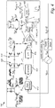
- Fig. 4 shows an example block diagram of an integrated calibration loop 140.
- the perturbation of the oscillation amplitude, ⁇ V amp is used in the loop 140 as a stimulus to calibrate G opt .
- the outputs of the oscillator may be first connected to a peak detector 410.
- the output V pd of the peak detector 410 contains two frequency components: the desired one at f ripple , and the additional one at the second harmonic of the oscillation frequency, f osc .
- V pd may then be amplified through self-biased inverters.
- the inverter stages 422, 424 may be implemented.
- the inverter stages 422, 424 amplify the small input level at V pd (e.g. 1 mV) to a larger amplitude (e.g. , 250 mV) at the output V inv , with a relatively large gain (e.g. 48 dB).
- the output of the inverter chain, V inv may be filtered by an RC low-pass filter (LPF) 430.
- the cut-off frequency of the LPF 430 may be set to pass through the desired frequency component at f ripple , while the second harmonic at 2 ⁇ f osc is filtered out. If there is any mismatch in the input differential pair of the peak detector, V pd would contain a third frequency component at f osc . Since f osc (several GHz) is much higher than f ripple (tens of MHz), this component is filtered out by the inverter chain and the LPF. Hence, the mismatch in the peak detector will not affect the calibration results.
- the calibration block 140 comprises a detector - comprising the peak detector 410, the amplifier 420, and the LFP 430 - configured to detect the amplitude variation ⁇ V amp of the oscillating signal output V osc of the LC oscillator 110.
- V ref is roughly set to a voltage higher than the product of the desired ⁇ V amp and the DC gain of the peak detector 410 cascade with the inverter stages 422, 424.
- the output V out of the comparator 440 may be connected to the clock terminal of a D flip-flop (DFF) 450.
- DFF D flip-flop
- a digital algorithm in the loop monitors the latch output, Latch_out, and may calculate the optimum control code S t (see below) for the ripple replication block 130. Other ways of controlling the replication block 130 are equally possible.
- the digital block 460 attempts to find the minimum point of ⁇ V amp vs. the control code ( ⁇ V amp,min in Fig. 5a).
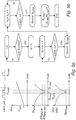
- Fig. 5a shows the operating principle of the proposed technique.
- the reference voltage, V ref at the comparator input is roughly set to a value corresponding to an oscillation amplitude variation of ⁇ V amp,th , which is higher than ⁇ V amp,min .
- the calibration process starts from a small value of S t , where G ⁇ G opt and ⁇ V amp > ⁇ V amp,th .
- the initial value of Latch_out is '1'.
- the algorithm keeps increasing S t , which decreases ⁇ V amp as G approaches G opt .
- the LC powering arrangement 100 is configured so that, during the minimizing of the amplitude variation ⁇ V amp , the reference voltage V ref is set to a value larger than a minimum ⁇ V amp,min of the amplitude variation, a controller, here in the form of digital block 460, being configured to determine the optimum value G opt of the tunable fractional gain G as an average of a lower gain corresponding to a first output transition of the comparator 440 and a higher gain corresponding to a second output transition of the comparator 440.
- a calibration algorithm is proposed whereby only one comparator 440 without any offset calibration needs to be used in the loop. Otherwise, to precisely detect ⁇ V amp,min , a set of comparators and DFFs would be needed.
- the simulated amplitude variation at the output of the LPF is ⁇ 300 mV.
- 20 comparators, followed by a DFF each are able to achieve a voltage resolution of 15 mV.
- Some offset calibration techniques would also have been needed to reduce the input referred offset of comparators to a level much lower than the voltage resolution.
- the digital algorithm would then count the number of '1's in the output of the DFFs to determine ⁇ V amp . Such a method would increase the design complexity greatly.
- the method of the present disclosure achieves an accurate determination of ⁇ V amp,min while retaining low design complexity.
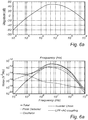
- Fig. 6b shows the simulated power spectrum density (PSD) of noise at the comparator's input.
- PSD power spectrum density
- a major part of the noise is contributed by the oscillator itself.
- the differential output of the oscillator is less affected by the variation of the common mode voltage, but the output level of the peak detector would be modulated.
- the calibration loop 140 is more sensitive to the common mode noise from the oscillator 110, e.g. noise of the supply current source.
- the common-mode noise is finally passed to the comparator's 440 input. From Fig.
- the integrated noise is around 14 mV, corresponding to ⁇ 0.095 mV equivalent input noise at the input of the peak detector at 5 MHz f ripple .
- ⁇ V amp is simulated to be ⁇ 1.8 mV (0.64 mV rms ), leading to a SNR of 16.5 dB, which is sufficient for an effective calibration.
- Fig. 7 shows a schematic of an example ripple replication block 130 together with an example LC oscillator 110.
- the ripple replication block 130 is proposed to bias the gate terminal of current source M 0 of the LC oscillator 110.
- the ripple replication block 130 is logically divided into two parts.
- the first part 132 (left dashed box in Fig. 7 ) contains a diode-connected PMOS transistor, M b0 , in series with two cascode NMOS transistors, M b1,2 . Due to the high output impedance of the cascode, M b0 just 'replicates' the supply ripple to V b0 with a fixed and unitary gain of 1.
- the first term on the right hand side of equation 3 is covered by this part.
- the fractional part 134 (right dashed box in Fig. 7 ) is introduced to inject some extra current proportional to V DD into the cascode node, V inj .
- the tunable fractional gain is settable by a n -bit digital code, where n is a predetermined integer and the fractional part of the replication block comprises n injection blocks each individually switchable by an individual bit in the n -bit digital code.
- the fractional part thus provides an adjustable transconductance between V DD and V inj .
- the final gain G provided by the ripple replication block 130 can be approximated as G ⁇ 1 + g m , f g m , b 0 where g m,f and g m,b0 are the total equivalent transconductance of the fractional part 134 and the transconductance of M b0 , respectively. Since G opt is only slightly larger than 1, the required g m,f should be much smaller than g m,b0 . Therefore, the total current injected into V inj is much smaller than the current consumed by M b0 , and would not lead to a large variation of the operating point of the LC oscillator. Moreover, the cascode transistor M b1 could be removed for designs with lower V DD . The slightly reduced gain provided by the first part could be compensated by slightly increasing g m,f .
- a channel length of 120 nm is used for M 0 leading to a load of ⁇ 800 fF.
- the total current consumption (including the fractional part) is ⁇ 200 ⁇ A with a maximum G of ⁇ 1.1.
- a 5-bit thermometer code is implemented to cover the aforementioned maximum G.
- the PMOS transistors in the fractional part are sized to achieve tuning resolution of ⁇ 0.003 as a trade-off between the resolution and calibration time.
- the unit-gain bandwidth, ⁇ u of the ripple replication block is established by both the frequency of the supply ripple, f ripple , and the tolerable phase shift between the ripple and the replica.
- a complementary cross-coupled oscillator structure may be chosen. This leads to lower power consumption compared to its NMOS- and PMOS-only counterparts at same V DD and equivalent parallel resistance of the tank.
- the designed oscillator uses a transformer-based resonant tank. Since the ripple replication block is connected to the gate of supply current source M 0 , the replicator's output noise (see Fig. 8a ), especially flicker noise of transistors M b0,2 , will modulate the oscillator's current, thus up-converting into output phase noise (PN) through a mechanism such as Groszkowski's effect. An implicit common-mode resonance technique is applied, which limits PN degradation.
- Single-ended capacitor banks are connected to a symmetrical transformer, as shown in Fig. 8b , are used to tune the common-mode resonance frequency to around 2 ⁇ f osc .
- Simulation results in Fig. 8c show that the PN degradation can be reduced to ⁇ 1 dB when the implicit common-mode technique is used.
- Both the NMOS and PMOS cross-coupled transistors M 1-4 provide the negative transconductance in the complementary structure.
- the body terminals of the PMOS cross-coupled pair, M 1,2 are deliberately connected to their source terminals to avoid the body effect. Otherwise, their threshold voltage, V th , would be modulated under supply variations thus varying the oscillation amplitude V osc , consequently pushing f osc .
- Simulation results show that the supply pushing due to this body effect could be as high as 9.5 MHz/V. Note that the above mentioned NMOS alternative to the supply current transistor M 0 would not be effective unless a costly triple-well technology is used.
- the example LC oscillator 110 with the proposed powering arrangement 100 with feed-forward ripple replication and cancellation was implemented in TSMC 40-nm 1 P8M CMOS process without ultra-thick metal layers.
- the proposed calibration loop 140 was also integrated on-die.
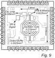
- Fig. 9 shows the chip micrograph.
- the total active area is 0.23 mm 2 , in which the oscillator core occupies about 0.215 mm 2 .
- the additional area occupied by the ripple replication block with its biasing circuit and the calibration loop 140 is just 0.012 mm 2 .
- the symmetrical transformer was designed by stacking the top two metal layers with the aluminum capping layer, which enhances the tank's Q-factor.
- the spacing between each turn of the transformer was optimized for a magnetic coupling factor of 0.31.
- the simulated differential inductance of the transformer is 1.7 nH.
- the Q-factor of the whole tank is estimated to be ⁇ 7.
- the capacitor banks are split into a 5-bit differential bank and a 5-bit common
- the measured tuning range (TR) is 4.9-5.7 GHz (15%).
- Fig. 10a shows the measured PN performance across the TR. PN varies from -108 to -111 dBc/Hz @1 MHz offset, with a flicker noise corner of around 100 kHz.
- the control code S t of the ripple replication block is manually swept while a 50 mV pp (peak-to-peak) 5 MHz sinusoidal ripple is applied on the oscillator supply.
- Fig. 12a The effectiveness of the automatic calibration loop 140 is verified in Fig. 12a , which compares the spectra before and after the calibration. With the supply contamination by a 50 mV pp 5 MHz sinusoidal ripple, the spur level is reduced by 30 dBc and reaches -68.7 dBc after the calibration.
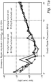
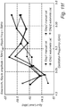
- Fig. 11a shows the measured spur level over the frequency of the supply ripple.
- the proposed technique achieves ⁇ -49 dBc optimum spur levels under ⁇ 50 mV pp , 0.5-20 MHz sinusoidal ripples, while the calibrated spur levels closely follow the optimum ones in most cases.
- the increase of the spur level at high ripple frequencies is due to the bandwidth limitation of the ripple replication block, and could be extended by expending more power.
- Fig. 12a The increase of the spur level at high ripple frequencies is due to the bandwidth limitation of the ripple replication block, and could be extended by expending more power.
- the spur level is measured across the tuning range of the oscillator.
- the worst-case spur under a 50 mV pp 5MHz sinusoidal ripple is ⁇ 59 dBc.
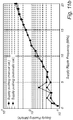
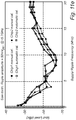
- Fig. 11b and Fig. 11d show the oscillator's supply pushing based on the measured spur levels. When the ripple frequency is lower than 12 MHz, the calculated supply pushing is lower than 1 MHz/V for both the optimum and calibrated cases.
- Fig. 12b compares the spectra before and after the calibration. Under a 50 mV pp 5 MHz saw-tooth ripple, the spur at the fundamental offset is reduced by 22.9 dB and reaches -61.7 dBc after the calibration. For spurs at higher harmonics, the suppression is also observed, but with lower magnitudes (5.8 dBc suppression for the second harmonic reaching -59.1 dBc after the calibration).
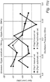
- Fig. 11e shows the spur levels over the ripple frequency. The worst-case spur of -47 dBc is found under ⁇ 50 mV pp , 0.5-20 MHz saw-tooth ripples, while the calibration results follow the optima. In Fig. 11f , the spurs are lower than -58 dBc within the entire tuning range under a 50 mV pp 5 MHz saw-tooth ripple.
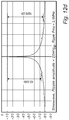
- Fig. 12c shows the measured oscillator spectrum under a 50 mV pp 2.5 MHz supply ripple.
- a spur can also be observed at an offset frequency of 5 MHz (i.e. 2 ⁇ 2.5 MHz).
- This second ripple harmonic spur mainly comes from the nonlinearity of the fractional part of the ripple replication block.
- the transistors in this part are biased with small overdrive voltage, resulting in V IP2 ⁇ 140 mV and g m / l ds ⁇ 19.
- these transistors need to be re-sized and biased with better linearity and smaller g m / l ds .
- the resulting increase in current consumption would be quite small (i.e.
- the spur at the second ripple harmonic reduces faster with the ripple amplitude.
- the measured spur level at the second harmonic is reduced to -65.9 dBc under a 20 mV pp ripple, which should bear little practical consequences.
- the IC chip was also measured over the temperature range of 0-80 °C, and the results are shown in Fig. 13 .
- the spur levels are lower than -60 dBc, except for the calibrated one at 80 °C.
- Table I summarizes the features and performance of the proposed technique.
- Table 1 Description Feed-forward compensation Osc. Type LC Tech. (nm) 40 (w/o UTM) V pp (V) 1.0 Frequency Range (GHz) 4.9 - 5.7 (15%) PN (dBc/Hz) @1 MHz -107.9 to -110.9 Ripple amplitude 50 mV pp Sinewave Spur (dBc) @1 MHz ⁇ -54 @5 MHz ⁇ -58 K sup (MHz/V) @1 MHz ⁇ 0.16* @5 MHz ⁇ 0.5* Improv.
- the proposed ripple replication block 130 generates an amplified supply ripple replica G A ripple at the gate terminal of the oscillator's 110 supply current source, in order to stabilize the supply current and oscillation amplitude under supply variations.
- the oscillation frequency is stabilized in turn, leading to ⁇ 1 MHz/V supply pushing for supply ripples up to 12 MHz.
- implicit common mode resonance is used in the resonant tank.
- a calibration loop 140 with a simple and effective algorithm is also integrated on-chip, which effectively finds the optimum gain G for the ripple replication block 130.
Landscapes
- Engineering & Computer Science (AREA)
- Power Engineering (AREA)
- Inductance-Capacitance Distribution Constants And Capacitance-Resistance Oscillators (AREA)
- Dc-Dc Converters (AREA)
Abstract
Description
- The present inventive concept relates to an LC oscillator powering arrangement and a method of powering an LC oscillator.
- Portable devices, such as Internet-of-Things (loT) devices, often include LC oscillators for radio communication purposes and may be powered by batteries or energy harvesters.
- The devices may need DC-DC converters to transform output levels from power sources to a nominal supply voltage of circuitry of the loT devices. However, switching operation of the DC-DC converters may cause output ripples in supply voltage. Such ripples may severely degrade performance of circuitry that is sensitive to the supply voltage. For instance, ripples in supply voltage to an LC oscillator may cause periodic amplitude variations and the LC oscillator to output a varying oscillating frequency leading to large spurs in the LC oscillator output spectrum.
- An objective of the present inventive concept is to provide an LC oscillator powering arrangement which may ensure that an oscillation frequency output by the LC oscillator is accurately controlled.
- This and other objectives of the present inventive concept are at least partly met by the invention as defined in the independent claims. Preferred embodiments are set out in the dependent claims.
- According to an aspect of the present inventive concept there is provided an LC oscillator powering arrangement, comprising an LC oscillator configured to provide an oscillating signal output; a current source configured to supply the LC oscillator with a supply current, the current source during operation being controlled by a control voltage and supplied with a supply voltage subject to supply voltage ripple; and a replication block configured to generate an optionally amplified replica of the supply voltage ripple directly from the supply voltage and to overlay the replica on the control voltage.
- Ripple present on the supply voltage will affect the current supplied by the current source to the LC oscillator, resulting in a time-varying oscillation amplitude. By overlaying a replica of the supply voltage ripple on the control voltage controlling the current source, this effect may be compensated for.
- The replication block may be configured to generate a replica of the supply voltage ripple or an amplified replica of the supply voltage ripple. Thus, the generated replica may have the same amplitude as the ripple, be amplified with a pre-determined gain, or be amplified with a variable gain settable in a calibration procedure.
- The LC oscillator powering arrangement according to the first aspect is configured to generate an optionally amplified replica of a ripple directly from the supply voltage. Generating the replica directly from the supply voltage should be understood as the replica being generated, over the cycle of periodic variations (ripple) of the supple voltage, only from that supply voltage and not, for example, based in whole or part on the output of the LC oscillator. Using such a replica generated directly from the supply voltage, instead of, for example, from detection of the time-varying amplitude of the LC oscillator output, avoids delay effects in the LC oscillator and detection circuitry, leading to better compensation for the supply voltage ripple.
- Thanks to the LC oscillator power arrangement being able to provide a stable supply current, despite supply voltage ripple, a need for power-consuming linear regulators, such as low-dropout linear regulators (LDOs), may be avoided. This allows the LC oscillator to be run directly on the output of a DC-DC converter, such as a switched-mode power supply. Hereby, power is saved.
- According to one embodiment, the LC oscillator powering arrangement further comprises a calibration block, where the replication block is configured to amplify the replica with a tunable fractional gain settable by the calibration block, the calibration block being connected to the oscillating signal output of the LC oscillator and configured to minimize the amplitude variation of the oscillating signal output of the LC oscillator by determining an optimum value of the tunable fractional gain of the replication block.
- This calibration is performed on a time scale longer, and typically much longer, than the cycle of periodic variations (ripple) of the supple voltage.
- The current source may be controlled to output a stable supply current despite supply voltage ripple by providing a replica of the supply voltage ripple to the control voltage. However, a replica on the control voltage based on a fixed pre-determined gain may not perfectly compensate for the supply voltage ripple. In particular, the arrangement may be affected by process, voltage and temperature (PVT) variations. Thus, the replica of the ripple may be amplified with an adjustable gain in order to ensure that a compensation for supply voltage ripple is provided, which is insensitive to PVT variations.
- Using the calibration block, the oscillating signal may be analyzed in order to set a gain that include compensation for PVT variations or any other factors causing variation in the optimal gain between the supply voltage ripple and the replica.
- The replication block may be configured to amplify the replica with a gain that is a combination of a fixed gain and a tunable fractional gain, which is set by the calibration block.
- The fixed gain may be set to 1, whereas an appropriate tunable fractional gain may be determined by the calibration block in order to determine a suitable compensation for supply voltage ripple.
- This allows the gain of the replica to be fine-tuned for optimal attenuation of the amplitude variation of the LC oscillator output.
- According to one embodiment, the calibration block comprises a detector configured to detect an amplitude variation of the oscillating signal output of the LC oscillator; a comparator comparing the amplitude variation with a reference voltage; and a controller connected to the comparator and configured to set the tunable fractional gain of the replication block during calibration.
- Using the detector and the comparator, the calibration block may be configured to determine how the amplitude variation is affected by tuning the fractional gain. This may be used in order to determine an optimum value of the tunable fractional gain, which may then be set by the controller.
- According to one embodiment, the LC powering arrangement is configured so that, during the minimizing of the amplitude variation, the reference voltage is set to a value larger than a minimum of the amplitude variation, the controller being configured to determine the optimum value of the tunable fractional gain as an average of a lower gain corresponding to a first output transition of the comparator and a higher gain corresponding to a second output transition of the comparator.
- This allows the optimal gain of the replica to be accurately determined in a relatively simple circuit, reducing complexity and thereby power consumption and cost.
- According to one embodiment, the current source is a MOS transistor.
- Thus, the current source may be implemented as a simple circuit component, which implies that the LC oscillator powering arrangement may be compact.
- According to one embodiment, the current source is a PMOS transistor, the supply voltage is applied at a source terminal of the PMOS transistor, the control voltage is applied at a gate terminal of the PMOS transistor, and the supply current is drawn from a drain terminal of the PMOS transistor.
- The supply current of the PMOS transistor may for an ideal device be controlled by a gate-to-source voltage. By providing a replica of the supply voltage ripple at the gate terminal, the supply voltage ripple provided at the source terminal may be compensated for.
- However, for nanoscale PMOS transistors, the supply current may also depend on a drain-to-source voltage. This implies that an amplified replica of the supply ripple may be needed.
- The use of a calibration block for providing a tunable fractional gain may be advantageous in ensuring that an appropriate amplification of the supply ripple is used, which may be compensate for PVT variations.
- According to one embodiment, the tunable fractional gain is settable by a n-bit digital code, where n is a predetermined integer.
- This implies that a predetermined resolution of setting the tunable fractional gain may be used and that a trade-off between the time for determining the optimum value of the tunable fractional gain by the calibration block and the achievable resolution may be made, given a chosen dynamic range for the gain, by setting the predetermined integer.
- According to one embodiment, the replication block comprises a replicating part, providing unitary gain, and a fractional part providing the tunable fractional gain, the fractional part comprising n injection blocks each individually switchable by an individual bit in the n-bit digital code.
- This implies that the digital code may be used in order to quickly control the gain of the replication block, since an injection block may easily be controlled to contribute to the gain in dependence on a bit of the digital code.
- According to one embodiment, the replicating part comprises a diode-connected PMOS transistor in series with two NMOS transistors forming a cascode, and each of the injection blocks comprises a current-source PMOS transistor in series with a switching PMOS transistor, a gate terminal of the switching PMOS transistor being connected to a corresponding the individual bit of the digital code and a drain terminal of the switching PMOS transistor being connected to a node of the cascode.
- The replicating part may provide a unitary gain. By connecting a drain of the switching PMOS transistor to a node of the cascode of the replicating part, a fractional gain may be added to the unitary gain based on a signal, corresponding to the individual bit of the digital code, provided on the gate terminal of the switching PMOS transistor.
- According to one embodiment, the detector comprises a peak detector, an amplifier, and a low-pass filter.
- The peak detector may detect an amplitude variation of the oscillating signal output of the LC oscillator. This amplitude variation may further be amplified in order to facilitate detection of the amplitude variation. Further, the low-pass filter may ensure that the amplitude variation may be separated from an oscillation frequency of the LC oscillator and harmonics thereof.
- According to one embodiment, the LC oscillator powering arrangement is provided on a single chip.
- This implies that the LC oscillator powering arrangement may be compact and small size, ensuring that the LC oscillator powering arrangement is suitable for use e.g. in loT devices.
- According to another aspect of the present inventive concept, there is provided a method of powering an LC oscillator, the method desensitizing the LC oscillator from supply voltage ripple and comprising: applying a supply voltage driving a current source, the supply voltage being subject to supply voltage ripple; generating and optionally amplifying a replica of the supply voltage ripple directly from the supply voltage; and applying a control voltage at the current source, the control voltage being overlaid with the replica, supplying the LC oscillator with a supply current from the current source.
- Effects and features of this second aspect are largely analogous to those described above in connection with the first aspect. Embodiments mentioned in relation to the first aspect are largely compatible with the second aspect.
- By applying a control voltage at a current source, wherein the control voltage is overlaid with a replica of supply voltage ripple generated directly from the supply voltage, a good compensation of the supply voltage ripple on the supply current generated may be provided.
- The above, as well as additional objects, features and advantages of the present inventive concept, will be better understood through the following illustrative and non-limiting detailed description, with reference to the appended drawings. In the drawings like reference numerals will be used for like elements unless stated otherwise.
-
Fig. 1a is a conceptual block diagram of an LC oscillator powering arrangement with the equivalent model. -
Fig. 1b is a conceptual block diagram of the proposed supply pushing reduction technique using a calibration loop. -
Fig. 2 shows simulation results of an LC oscillator with the proposed technique. -
Fig. 3 shows the operating principle of the calibration loop based on oscillation amplitude variation (ΔV osc). -
Fig. 4 is a block diagram of a calibration loop. -
Fig. 5a shows the operating principle of the calibration loop using a proposed algorithm. -
Fig. 5b is a flow chart of the calibration loop with the proposed algorithm. -
Fig. 6a shows a simulated transfer function from peak detector output to comparator input in the calibration loop. -
Fig. 6b shows a simulated power spectrum density of noise at comparator input with contributions from different noise sources. -
Fig. 7 is a schematic of an implemented LC oscillator with a ripple replication block. -
Fig. 8a shows the output noise of the ripple replication block. -
Fig. 8b shows a schematic of a symmetrical transformer of the LC oscillator. -
Fig. 8c shows the phase degradation of the LC oscillator with and without the common mode resonance. -
Fig. 9 shows a chip micrograph of the LC oscillator with reduced supply pushing. -
Fig. 10a shows measured phase noise of the oscillator across a gain tuning range of the calibration loop. -
Fig. 10b shows measured spur level over a control code S t provided by the calibration loop. -
Fig. 11a shows measured spur levels over sinusoidal ripple frequency; and -
Fig. 11b shows the corresponding supply pushing for both manual and automatic calibrations. -
Fig. 11c shows measured spur levels over the oscillation frequency under the sinusoidal ripple; and -
Fig. 11d shows the corresponding supply pushing for both manual and automatic calibrations. -
Fig. 11e shows measured spur levels over the frequency of sawtooth ripple; and -
Fig. 11f shows measured spur levels over the oscillation frequency under the sawtooth ripple. -
Fig. 12a shows measured oscillator spectra before and after calibration under 50 mV peak-to-peak 5MHz sinusoidal ripple. -
Fig. 12b shows measured oscillator spectra before and after calibration under 50mV peak-to-peak 5MHz saw-tooth ripple. -
Fig. 12c shows measured oscillator spectra under 50 mV peak-to-peak 2.5MHz sinusoidal ripple. -
Fig. 12d shows measured oscillator spectra under 20 mV peak-to-peak 2.5MHz sinusoidal ripple. -
Fig. 13 shows measured spur levels over 0-80 °C. - An LC oscillator powering arrangement is provided which is insensitive to supply voltage ripple so that an LC oscillator may provide a desired oscillation output frequency.
- In the following, the operating principle of a technique for avoiding that a variation in supply voltage pushes or affects an oscillation output frequency, wherein the technique is based on replication of supply voltage ripple and in order to cancel an effect of the supply voltage ripple, will be elaborated. Particular reference will be made to a detailed circuit realization of a 5 GHz LC oscillator with the proposed feed-forward supply pushing reduction technique and an on-chip calibration loop.
-
Fig. 1a illustrates the operating principle of providing supply pushing reduction. In an LCoscillator powering arrangement 100, anLC oscillator 110 comprising aresonant tank 120, comprising an inductor and a capacitor, and cross-coupled transistors M1 , M2, M3 and M4 is supplied with current I0 from a current source. - In this embodiment, the current source is illustrated as being implemented by way of a MOS transistor, in this example a PMOS transistor M0, supplying the
LC oscillator 110 with a supply current I0. The transistor M 0 is supplied with voltage VDD , which is applied at its source terminal, and controlled by a control voltage Vb0, which is applied at its gate terminal. To stabilize I0, and thus the oscillating signal output Vosc being output by theLC oscillator 110, in face of VDD variations, a replica G A ripple of the supply ripple A ripple is generated at aripple replication block 130, directly from the supply voltage VDD , and overlaid on the gate of PMOS current source transistor M0. In the simplest case, if the replica is an exact copy of the supply voltage, i.e., G = 1, the gate-to-source voltage Vgs of the PMOS current source transistor M0 will be stabilized. As a result, the variation of I0 , and thereby of Vosc , will largely be suppressed. - The variation of oscillating frequency fosc of the
LC oscillator 110 with the supply voltage, VDD , is mainly caused by the variation of parasitic capacitances seen by theresonant tank 120. The cross-coupled transistors M1-M4 provide a negative transconductance to sustain the oscillation and will experience cut-off, saturation and triode operating regions during each oscillation cycle. When VDD varies, the supply current, I 0, and the corresponding oscillation amplitude, V osc, will also vary. Thus it will change the time interval during which the transistors stay in each operating region. Since the gate capacitance of MOS transistors shows nonlinear dependence on the voltages at their terminals (i.e. gate-to-source voltage V gs and drain-to-source voltage V ds), the change in the operating states of MOS transistors would vary the equivalent parasitic capacitance, C par,equ. Thus, the oscillating frequency will be pushed. If a periodical ripple is on VDD , I 0 and Vosc will also show periodical variations. Therefore, the change of C par,equ will also be periodical and could manifest itself as large spurs in the output spectrum of theLC oscillator 110. Stabilizing I 0 and V osc under VDD variations allows a clean output spectrum to be obtained when V DD contains ripples. - If M0 is an ideal device, whose drain current is solely controlled by its Vgs according to the square law, then an exact copy of the supply ripple waveform is required at its gate terminal Vb0 to keep I0 and V osc constant. However, for nanoscale CMOS technologies, a channel-length modulation effect is not negligible. This means that the drain current of M0 also depends on its Vds. Thus in order to compensate for residue current variation due to the variation of Vds of M0, it may be advantageous to use an amplified replica of the supply ripple in the waveform at Vb0
-
Fig. 1a also shows the equivalent model to estimate the optimum gain (Gopt ). Based on this model, the supply voltage variation, ΔVDD , induced supply current variation, ΔI 0,VDD , could be calculated as

tank 120 that is seen by M0 , while gm0 and ro0 are the effective transconductance and output resistance of M0 , respectively. To compensate for the supply current variation due to Vds , the magnitudes of (1) and (2) should be equal. Hence, G opt may be calculated as
- As shown in simulation results in
Fig. 2 , the variations of I0 and V osc do get largely suppressed when the waveform applied at Vb0 is the same as that of the supply ripple (gain, G = 1). Hence, the frequency variations due to the supply voltage are largely reduced, resulting in a much lower supply pushing of the oscillator.Fig. 2 also shows that I0 and V osc are further stabilized (i.e. ∼10 times smaller variations compared to the G = 1 case) under supply variations when G ≈ G opt, thus the supply pushing of the oscillator becomes much lower. - Portable devices such as Internet-of-Things (loT) devices powered by batteries or energy harvesters generally need buck and/or switching DC-DC converters to transform the output levels of energy sources to the nominal supply voltage of loT electronic circuitry. Due to the switching operation of DC-DC converters, the resulting output ripples can severely degrade performance of the supply-sensitive circuitry, such as LC-tank oscillators, when connected directly. This supply pushing of LC-tank oscillators, even those at state-of-the-art, needs to be substantially reduced to allow them to operate from DC-DC converters, which naturally contain high level of ripples. To avoid this, a low dropout (LDO) linear regulator is usually inserted after the switching converter to stabilize the supply voltage. However, the extra voltage overhead (∼200 mV) will worsen the system's power efficiency (∼80% under 1V supply). This will make it even more critical with the supply scaling down with technology.
- In the present disclosure, there is proposed a feed-forward supply ripple replication and cancellation technique which may be wholly contained within an LC oscillator in order to make it practically insensitive to supply ripples of switching DC-DC converters. Since, in the present disclosure, the LC oscillator may be driven directly from the output of the DC-DC converter, no extra voltage headroom is required. Therefore, power is saved.
- Optionally, a calibration block, here in the form of a
calibration loop 140, may also be implemented, optionally integrated on-die, as shown inFig. 1b . Thereplication block 130 is configured to amplify the replica with a tunable fractional gain settable by thecalibration block 140, with thecalibration block 140 being connected to the oscillating signal output V osc of the LC oscillator. - As can be gathered from
equation 3, the optimum gain is prone to PVT variations. Thecalibration loop 140 may compensate for such variations, improving performance as compared to using a pre-determined gain. - The calibration scheme is based on measuring the variation of the oscillation amplitude, ΔVamp , in response to the VDD perturbations.
Fig. 3 shows the operating principle of thecalibration loop 140. When G < G opt (case A), ΔI0,Vbo is smaller than ΔI0,VDD , so ΔV amp is in phase with ΔVDD and decreases in magnitude as G gets closer to G opt. However, when G > G opt (case B), ΔI0,Vb0 becomes larger than ΔI0,VDD. Then, ΔVamp is out of phase with ΔVDD , and its magnitude increases again with the increase of G. At the optimum point, G = G opt, and ideally a constant oscillation amplitude is maintained under supply variations. - Thus, the
calibration loop 140 may be configured to measure ΔV amp under different gain settings to calculate the optimum operating point for the oscillator circuit. Thus, thecalibration block 140 is configured to minimize the amplitude variation ΔVamp of the oscillating signal output V osc of theLC oscillator 110 by determining an optimum value of a tunable fractional gain G of thereplication block 130. Thecalibration loop 140 may be configured to only be active during calibration. -
Fig. 4 shows an example block diagram of anintegrated calibration loop 140. As discussed above, the perturbation of the oscillation amplitude, ΔV amp, is used in theloop 140 as a stimulus to calibrate G opt. The outputs of the oscillator may be first connected to apeak detector 410. Ideally, the output Vpd of thepeak detector 410, contains two frequency components: the desired one at f ripple, and the additional one at the second harmonic of the oscillation frequency, f osc. Vpd may then be amplified through self-biased inverters. - Two inverter stages 422, 424 with bandwidth of ∼20 MHz may be implemented. The inverter stages 422, 424 amplify the small input level at Vpd (e.g. 1 mV) to a larger amplitude (e.g., 250 mV) at the output V inv, with a relatively large gain (e.g. 48 dB).
- The output of the inverter chain, Vinv , may be filtered by an RC low-pass filter (LPF) 430. The cut-off frequency of the
LPF 430 may be set to pass through the desired frequency component at f ripple, while the second harmonic at 2 × f osc is filtered out. If there is any mismatch in the input differential pair of the peak detector, Vpd would contain a third frequency component at f osc. Since f osc (several GHz) is much higher than f ripple (tens of MHz), this component is filtered out by the inverter chain and the LPF. Hence, the mismatch in the peak detector will not affect the calibration results. - The resulting transfer function from
amplifier 420 input Vpd toLPF 430 output V lpf is shown as a function of frequency inFig. 6a . - Thus, the
calibration block 140 comprises a detector - comprising thepeak detector 410, theamplifier 420, and the LFP 430 - configured to detect the amplitude variation ΔV amp of the oscillating signal output V osc of theLC oscillator 110. - The output of the
LPF 430, V lpf, may then be compared with a reference value, V ref, through acomparator 440. V ref is roughly set to a voltage higher than the product of the desired ΔV amp and the DC gain of thepeak detector 410 cascade with the inverter stages 422, 424. - The output Vout of the
comparator 440 may be connected to the clock terminal of a D flip-flop (DFF) 450. When V ref is crossed, the comparator's 440 output becomes high, triggering the output of the DFF to flip to '1'. A digital algorithm in the loop monitors the latch output, Latch_out, and may calculate the optimum control code St (see below) for theripple replication block 130. Other ways of controlling thereplication block 130 are equally possible. - The
digital block 460 attempts to find the minimum point of ΔV amp vs. the control code (ΔV amp,min inFig. 5a). Fig. 5a shows the operating principle of the proposed technique. The reference voltage, V ref, at the comparator input is roughly set to a value corresponding to an oscillation amplitude variation of ΔV amp,th, which is higher than ΔV amp,min. The calibration process starts from a small value of St , where G < G opt and ΔV amp > ΔV amp,th. Thus, the initial value of Latch_out is '1'. The algorithm keeps increasing St , which decreases ΔV amp as G approaches G opt. When ΔV amp becomes lower than ΔV amp,th, Latch_out changes from '1' to '0'. The algorithm records this code as S t,min, and then increases St again. When S t is large enough, ΔV amp would be higher than ΔV amp,th again, and Latch_out switches back to 1. The algorithm records this code as S t,max, and the optimum code, S t,avg, is calculated as the average of these two recorded codes.Fig. 5b reveals the operational flow chart of this calibration process. The high-pass response of the loop due to AC-coupling limits the settling time when St changes. In this example, the corner frequency is designed to be ∼2.5 MHz, resulting in a settling time of 0.4 µs per step. Lower corner frequency could be used to detect lower ripple frequency at the expense of longer settling time. - Thus, the
LC powering arrangement 100 is configured so that, during the minimizing of the amplitude variation ΔV amp, the reference voltage V ref is set to a value larger than a minimum ΔV amp,min of the amplitude variation, a controller, here in the form ofdigital block 460, being configured to determine the optimum value G opt of the tunable fractional gain G as an average of a lower gain corresponding to a first output transition of thecomparator 440 and a higher gain corresponding to a second output transition of thecomparator 440. - Thus, in the present disclosure, a calibration algorithm is proposed whereby only one
comparator 440 without any offset calibration needs to be used in the loop. Otherwise, to precisely detect ΔV amp,min, a set of comparators and DFFs would be needed. The simulated amplitude variation at the output of the LPF is ∼300 mV. Thus, 20 comparators, followed by a DFF each, are able to achieve a voltage resolution of 15 mV. Some offset calibration techniques would also have been needed to reduce the input referred offset of comparators to a level much lower than the voltage resolution. The digital algorithm would then count the number of '1's in the output of the DFFs to determine ΔV amp. Such a method would increase the design complexity greatly. Thus, the method of the present disclosure achieves an accurate determination of ΔV amp,min while retaining low design complexity. -
Fig. 6b shows the simulated power spectrum density (PSD) of noise at the comparator's input. A major part of the noise is contributed by the oscillator itself. The differential output of the oscillator is less affected by the variation of the common mode voltage, but the output level of the peak detector would be modulated. Thus, thecalibration loop 140 is more sensitive to the common mode noise from theoscillator 110, e.g. noise of the supply current source. After being shaped by the transfer function of theinverter chain 420 andLPF 430, the common-mode noise is finally passed to the comparator's 440 input. FromFig. 6b , the integrated noise is around 14 mV, corresponding to ∼0.095 mV equivalent input noise at the input of the peak detector at 5 MHz f ripple. To achieve less than -50dBc spur level, ΔVamp is simulated to be ∼1.8 mV (0.64 mVrms), leading to a SNR of 16.5 dB, which is sufficient for an effective calibration. -
Fig. 7 shows a schematic of an exampleripple replication block 130 together with anexample LC oscillator 110. Theripple replication block 130 is proposed to bias the gate terminal of current source M 0 of theLC oscillator 110. To generate the required replica with the desired gain G larger than 1, theripple replication block 130 is logically divided into two parts. The first part 132 (left dashed box inFig. 7 ) contains a diode-connected PMOS transistor, M b0, in series with two cascode NMOS transistors, M b1,2. Due to the high output impedance of the cascode, M b0 just 'replicates' the supply ripple to V b0 with a fixed and unitary gain of 1. Thus, the first term on the right hand side ofequation 3 is covered by this part. - To boost the gain above 1, the fractional part 134 (right dashed box in
Fig. 7 ) is introduced to inject some extra current proportional to V DD into the cascode node, V inj. To digitally control the fractional gain, current source PMOS transistors M pk (k = 0, 1, ... n) are individually turned on/off by switch PMOS transistors M sk (k = 0, 1, ... n) according to the digital code S t generated by thecalibration loop 140. Switching PMOS transistor M pk drain terminal is connected to the node V inj of the cascode. - Thus, the tunable fractional gain is settable by a n-bit digital code, where n is a predetermined integer and the fractional part of the replication block comprises n injection blocks each individually switchable by an individual bit in the n-bit digital code.
- The fractional part thus provides an adjustable transconductance between V DD and V inj. The final gain G provided by the
ripple replication block 130 can be approximated as
fractional part 134 and the transconductance of Mb0 , respectively. Since Gopt is only slightly larger than 1, the required gm,f should be much smaller than gm,b0 . Therefore, the total current injected into Vinj is much smaller than the current consumed by Mb0, and would not lead to a large variation of the operating point of the LC oscillator. Moreover, the cascode transistor Mb1 could be removed for designs with lower VDD. The slightly reduced gain provided by the first part could be compensated by slightly increasing gm,f . - In this design, a channel length of 120 nm is used for M0 leading to a load of ∼800 fF. When gm /lds ≈ 12, the total current consumption (including the fractional part) is ∼200 µA with a maximum G of ∼1.1. A 5-bit thermometer code is implemented to cover the aforementioned maximum G. The PMOS transistors in the fractional part are sized to achieve tuning resolution of ∼0.003 as a trade-off between the resolution and calibration time. The unit-gain bandwidth, ωu , of the ripple replication block is established by both the frequency of the supply ripple, f ripple, and the tolerable phase shift between the ripple and the replica. To guarantee < -50 dBc spur level at f ripple = 20 MHz, a ωu of 450 MHz is required based on simulations. Together with the capacitive load at the output of the ripple replication block, this bandwidth requirement determines the current consumption of this block. A smaller capacitance could be achieved when M0 is designed with a minimum channel length. However, the required G opt would increase, which could adversely affect the tuning resolution and/or calibration time. The present design provides a compromise.
- For the
LC oscillator 110, as in this example, a complementary cross-coupled oscillator structure may be chosen. This leads to lower power consumption compared to its NMOS- and PMOS-only counterparts at same VDD and equivalent parallel resistance of the tank. The designed oscillator uses a transformer-based resonant tank. Since the ripple replication block is connected to the gate of supply current source M0 , the replicator's output noise (seeFig. 8a ), especially flicker noise of transistors Mb0,2 , will modulate the oscillator's current, thus up-converting into output phase noise (PN) through a mechanism such as Groszkowski's effect. An implicit common-mode resonance technique is applied, which limits PN degradation. Single-ended capacitor banks are connected to a symmetrical transformer, as shown inFig. 8b , are used to tune the common-mode resonance frequency to around 2 × f osc. Simulation results inFig. 8c show that the PN degradation can be reduced to < 1 dB when the implicit common-mode technique is used. Both the NMOS and PMOS cross-coupled transistors M1-4 provide the negative transconductance in the complementary structure. The body terminals of the PMOS cross-coupled pair, M1,2 , are deliberately connected to their source terminals to avoid the body effect. Otherwise, their threshold voltage, Vth , would be modulated under supply variations thus varying the oscillation amplitude V osc, consequently pushing f osc. Simulation results show that the supply pushing due to this body effect could be as high as 9.5 MHz/V. Note that the above mentioned NMOS alternative to the supply current transistor M0 would not be effective unless a costly triple-well technology is used. - The
example LC oscillator 110 with the proposed poweringarrangement 100 with feed-forward ripple replication and cancellation was implemented in TSMC 40-nm 1 P8M CMOS process without ultra-thick metal layers. The proposedcalibration loop 140 was also integrated on-die.Fig. 9 shows the chip micrograph. The total active area is 0.23 mm2, in which the oscillator core occupies about 0.215 mm2. The additional area occupied by the ripple replication block with its biasing circuit and thecalibration loop 140 is just 0.012 mm2. The symmetrical transformer was designed by stacking the top two metal layers with the aluminum capping layer, which enhances the tank's Q-factor. The spacing between each turn of the transformer was optimized for a magnetic coupling factor of 0.31. The simulated differential inductance of the transformer is 1.7 nH. The Q-factor of the whole tank is estimated to be ∼7. The capacitor banks are split into a 5-bit differential bank and a 5-bit common-mode bank to tune the common-mode resonance frequency. - The measured tuning range (TR) is 4.9-5.7 GHz (15%).
Fig. 10a shows the measured PN performance across the TR. PN varies from -108 to -111 dBc/Hz @1 MHz offset, with a flicker noise corner of around 100 kHz. To verify the concept of the proposed technique, the control code St of the ripple replication block is manually swept while a 50 mVpp (peak-to-peak) 5 MHz sinusoidal ripple is applied on the oscillator supply. As shown inFig. 10b , there exists an optimum code at which the spur level is lower than -60 dBc, corresponding to a >27 dB improvement over the St =0 case. Note that G ≈ 1 when St =0, and the oscillator already benefits from the significantly reduced supply pushing. - The effectiveness of the
automatic calibration loop 140 is verified inFig. 12a , which compares the spectra before and after the calibration. With the supply contamination by a 50mV pp 5 MHz sinusoidal ripple, the spur level is reduced by 30 dBc and reaches -68.7 dBc after the calibration.Fig. 11a shows the measured spur level over the frequency of the supply ripple. The proposed technique achieves ≤ -49 dBc optimum spur levels under ≤50 mVpp, 0.5-20 MHz sinusoidal ripples, while the calibrated spur levels closely follow the optimum ones in most cases. The increase of the spur level at high ripple frequencies is due to the bandwidth limitation of the ripple replication block, and could be extended by expending more power. InFig. 11c , the spur level is measured across the tuning range of the oscillator. The worst-case spur under a 50 mVpp 5MHz sinusoidal ripple is ≤ 59 dBc.Fig. 11b andFig. 11d show the oscillator's supply pushing based on the measured spur levels. When the ripple frequency is lower than 12 MHz, the calculated supply pushing is lower than 1 MHz/V for both the optimum and calibrated cases. - Similar measurements were also performed for saw-tooth ripples.
Fig. 12b compares the spectra before and after the calibration. Under a 50mV pp 5 MHz saw-tooth ripple, the spur at the fundamental offset is reduced by 22.9 dB and reaches -61.7 dBc after the calibration. For spurs at higher harmonics, the suppression is also observed, but with lower magnitudes (5.8 dBc suppression for the second harmonic reaching -59.1 dBc after the calibration).Fig. 11e shows the spur levels over the ripple frequency. The worst-case spur of -47 dBc is found under ≤50 mVpp, 0.5-20 MHz saw-tooth ripples, while the calibration results follow the optima. InFig. 11f , the spurs are lower than -58 dBc within the entire tuning range under a 50mV pp 5 MHz saw-tooth ripple. -
Fig. 12c shows the measured oscillator spectrum under a 50 mVpp 2.5 MHz supply ripple. A spur can also be observed at an offset frequency of 5 MHz (i.e. 2×2.5 MHz). This second ripple harmonic spur mainly comes from the nonlinearity of the fractional part of the ripple replication block. To achieve fine tuning resolution, the transistors in this part are biased with small overdrive voltage, resulting in VIP2 ≈ 140 mV and gm /lds ≈ 19. To improve the performance at the second ripple these transistors need to be re-sized and biased with better linearity and smaller gm /lds. The resulting increase in current consumption would be quite small (i.e. ∼12 µA) since the current consumed by the fractional part is much smaller than that consumed by the integer part. Also, the spur at the second ripple harmonic reduces faster with the ripple amplitude. As shown inFig. 12c , the measured spur level at the second harmonic is reduced to -65.9 dBc under a 20 mVpp ripple, which should bear little practical consequences. - The IC chip was also measured over the temperature range of 0-80 °C, and the results are shown in
Fig. 13 . The spur levels are lower than -60 dBc, except for the calibrated one at 80 °C. - Table I summarizes the features and performance of the proposed technique.
Table 1 Description Feed-forward compensation Osc. Type LC Tech. (nm) 40 (w/o UTM) Vpp (V) 1.0 Frequency Range (GHz) 4.9 - 5.7 (15%) PN (dBc/Hz) @1 MHz -107.9 to -110.9 Ripple amplitude 50 mVpp Sinewave Spur (dBc) @1 MHz < -54 @5 MHz < -58 Ksup (MHz/V) @1 MHz < 0.16* @5 MHz < 0.5* Improv. (dBc) @1 MHz 18 - 24** @5 MHz 24 - 30** Saw-tooth Spur (dBc) @1 MHz < -50 @5 MHz < -58 Improv. (dBc) @1 MHz 11.3** @5 MHz 22 - 27** Osc. Power Cons. (mW) 0.8 - 1.3 Power Cons. K sup Reduction Tech. (mW) 0.2 Area of K sup Reduction Tech (mm2) 0.012 Total area (mm2) 0.23 * Calculated value from the spur level.
** Compared with the case St = 0 (G = 1) where the supply pushing of the oscillator is already suppressed. - With the present disclosure, it is possible to significantly reduce supply pushing in current-mode LC oscillators while consuming no extra voltage headroom. The proposed
ripple replication block 130 generates an amplified supply ripple replica G A ripple at the gate terminal of the oscillator's 110 supply current source, in order to stabilize the supply current and oscillation amplitude under supply variations. The oscillation frequency is stabilized in turn, leading to <1 MHz/V supply pushing for supply ripples up to 12 MHz. To suppress the phase noise degradation due to the extra circuitry, implicit common mode resonance is used in the resonant tank. Acalibration loop 140 with a simple and effective algorithm is also integrated on-chip, which effectively finds the optimum gain G for theripple replication block 130. - In the above the inventive concept has mainly been described with reference to a limited number of examples. However, as is readily appreciated by a person skilled in the art, other examples than the ones disclosed above are equally possible within the scope of the inventive concept, as defined by the appended claims.
Claims (12)
- An LC oscillator (110) powering arrangement (100), comprising:an LC oscillator (110) configured to provide an oscillating signal output (V osc);a current source (M0 ) configured to supply said LC oscillator (110) with a supply current (I 0), said current source (M0 ) during operation being controlled by a control voltage (Vb0 ) and supplied with a supply voltage (VDD ) subject to supply voltage ripple (A ripple); anda replication block (130) configured to generate an optionally amplified replica (G A ripple) of said supply voltage ripple (A ripple) directly from said supply voltage (Vb0 ) and to overlay said replica (G A ripple) on said control voltage (Vb0 ).
- The arrangement (100) of claim 1, further comprising a calibration block (140), wherein said replication block (130) is configured to amplify said replica with a tunable fractional gain (G) settable by said calibration block (140), said calibration block (140) being connected to said oscillating signal output (V osc) of said LC oscillator (110) and configured to minimize an amplitude variation (ΔV amp) of said oscillating signal output (V osc) of said LC oscillator (110) by determining an optimum value (G opt) of said tunable fractional gain (G) of said replication block.
- The arrangement (100) of claim 2, wherein said calibration block (140) comprises:a detector configured to detect said amplitude variation;a comparator (440) comparing said amplitude variation (ΔV amp) with a reference voltage (V ref); anda controller (460) connected to said comparator (440) and configured to set said tunable fractional gain (G) of said replication block (130) during calibration.
- The arrangement (100) of claim 3, configured so that, during said minimizing of said amplitude variation (ΔV amp), said reference voltage (V ref) is set to a value larger than a minimum of said amplitude variation (ΔV amp), said controller being configured to determine said optimum value (G opt) of said tunable fractional gain (G) as an average of a lower gain corresponding to a first output transition of said comparator and a higher gain corresponding to a second output transition of said comparator.
- The arrangement (100) of any one of the preceding claims, wherein said current source (M0 ) is a MOS transistor.
- The arrangement (100) of claim 5, wherein said current source (M0 ) is a PMOS transistor, said supply voltage (VDD ) is applied at a source terminal of said PMOS transistor (M0 ), said control voltage is applied at a gate terminal of said PMOS transistor (M0 ), and said supply current is drawn from a drain terminal of said PMOS transistor (M0 ).
- The arrangement (100) of any one of claims 2-6, wherein said tunable fractional gain (G) is settable by a n-bit digital code (St ), wherein n is a predetermined integer.
- The arrangement (100) of claim 7, wherein said replication block (130) comprises a replicating part (132), providing unitary gain, and a fractional part (134) providing said tunable fractional gain (G), said fractional part (134) comprising n injection blocks each individually switchable by an individual bit in said n-bit digital code (St ).
- The arrangement (100) of claim 8, wherein said replicating part comprises a diode-connected PMOS transistor (Mb0) in series with two NMOS transistors (Mb1 , Mb2 ) forming a cascode, and each of said injection blocks comprises a current-source PMOS transistor (Mpk ) in series with a switching PMOS transistor (Msk ), a gate terminal of said switching PMOS transistor being connected to a corresponding said individual bit of said digital code (St ) and a drain terminal of said switching PMOS transistor being connected to a node of said cascode.
- The arrangement (100) of any one of claims 3-9, wherein said detector comprises a peak detector (410), an amplifier (420), and a low-pass filter (430).
- The arrangement (100) of any one of the preceding claims, provided on a single chip.
- A method of powering an LC oscillator (110), said method desensitizing said LC oscillator (110) from supply voltage ripple (A ripple) and comprising:applying a supply voltage (VDD ) driving a current source (M0 ), said supply voltage (VDD ) being subject to supply voltage ripple (A ripple);generating and optionally amplifying a replica of said supply voltage ripple (G A ripple) directly from said supply voltage (VDD ); andapplying a control voltage (Vb0 ) at said current source, said control voltage (Vb0 ) being overlaid with said replica (G A ripple),supplying said LC oscillator (110) with a supply current from said current source (M0 ).
Priority Applications (2)
| Application Number | Priority Date | Filing Date | Title |
|---|---|---|---|
| EP18175371.6A EP3576300A1 (en) | 2018-05-31 | 2018-05-31 | An lc oscillator powering arrangement and a method of powering an lc oscillator |
| US16/427,933 US10892710B2 (en) | 2018-05-31 | 2019-05-31 | LC oscillator powering arrangement and method of powering an LC oscillator |
Applications Claiming Priority (1)
| Application Number | Priority Date | Filing Date | Title |
|---|---|---|---|
| EP18175371.6A EP3576300A1 (en) | 2018-05-31 | 2018-05-31 | An lc oscillator powering arrangement and a method of powering an lc oscillator |
Publications (1)
| Publication Number | Publication Date |
|---|---|
| EP3576300A1 true EP3576300A1 (en) | 2019-12-04 |
Family
ID=62562954
Family Applications (1)
| Application Number | Title | Priority Date | Filing Date |
|---|---|---|---|
| EP18175371.6A Pending EP3576300A1 (en) | 2018-05-31 | 2018-05-31 | An lc oscillator powering arrangement and a method of powering an lc oscillator |
Country Status (2)
| Country | Link |
|---|---|
| US (1) | US10892710B2 (en) |
| EP (1) | EP3576300A1 (en) |
Cited By (1)
| Publication number | Priority date | Publication date | Assignee | Title |
|---|---|---|---|---|
| US11463045B2 (en) * | 2018-09-25 | 2022-10-04 | Sony Semiconductor Solutions Corporation | Oscillator circuit and radio receiver |
Citations (7)
| Publication number | Priority date | Publication date | Assignee | Title |
|---|---|---|---|---|
| US20020167366A1 (en) * | 2001-02-12 | 2002-11-14 | Sanduleanu Mihai Adrian Tiberiu | LC controllable oscillator, a quadrature oscillator and a communication arrangement |
| US7336134B1 (en) * | 2004-06-25 | 2008-02-26 | Rf Micro Devices, Inc. | Digitally controlled oscillator |
| US20080100350A1 (en) * | 2004-03-22 | 2008-05-01 | Mobius Microsystems, Inc. | Spread Spectrum Clock and Reference Signal Generator |
| US20100295626A1 (en) * | 2009-05-19 | 2010-11-25 | Electronics And Telecommunications Research Institute | Voltage-controlled oscillator robust against power noise and communication apparatus using the same |
| US20130271226A1 (en) * | 2011-07-01 | 2013-10-17 | Si-Ware Systems Inc. | Self-Biased Amplitude-Controlled Oscillator With Constant Harmonic Content |
| US20150280645A1 (en) * | 2014-03-25 | 2015-10-01 | Avago Technologies General Ip (Singapore) Pte. Ltd. | Inductive-Capacitive (LC) Voltage Controlled Oscillator (VCO) Having Tuning Range Controlled By A Digital-To-Analog Converter (DAC) With Programmable Tail Current |
| JP2017130819A (en) * | 2016-01-21 | 2017-07-27 | ソニー株式会社 | Variable capacitance circuit, oscillator circuit and control method for variable capacitance circuit |
Family Cites Families (10)
| Publication number | Priority date | Publication date | Assignee | Title |
|---|---|---|---|---|
| JP3860316B2 (en) * | 1997-12-24 | 2006-12-20 | 東芝マイクロエレクトロニクス株式会社 | Stabilized oscillation circuit |
| US6552618B2 (en) | 2000-12-13 | 2003-04-22 | Agere Systems Inc. | VCO gain self-calibration for low voltage phase lock-loop applications |
| US7355482B2 (en) | 2006-02-17 | 2008-04-08 | Seiko Epson Corporation | Methods and apparatus for compensating a variable oscillator for process, voltage, and temperature variations using a replica oscillator |
| US7948330B2 (en) | 2009-03-19 | 2011-05-24 | Qualcomm Incorporated | Current controlled oscillator with regulated symmetric loads |
| US8918070B2 (en) | 2012-05-04 | 2014-12-23 | Analog Devices, Inc. | Frequency tuning for LC circuits |
| WO2014013289A1 (en) | 2012-07-20 | 2014-01-23 | Freescale Semiconductor, Inc. | Calibration arrangement for frequency synthesizers |
| US9225231B2 (en) | 2012-09-14 | 2015-12-29 | Rf Micro Devices, Inc. | Open loop ripple cancellation circuit in a DC-DC converter |
| DE102014102940A1 (en) * | 2013-03-13 | 2014-09-18 | Analog Devices, Inc. | Oscillator with LC primary and secondary oscillations |
| US9634607B2 (en) | 2014-03-11 | 2017-04-25 | Qualcomm Incorporated | Low noise and low power voltage-controlled oscillator (VCO) using transconductance (gm) degeneration |
| US9552006B1 (en) | 2015-03-09 | 2017-01-24 | Inphi Corporation | Wideband low dropout voltage regulator with power supply rejection boost |
-
2018
- 2018-05-31 EP EP18175371.6A patent/EP3576300A1/en active Pending
-
2019
- 2019-05-31 US US16/427,933 patent/US10892710B2/en active Active
Patent Citations (7)
| Publication number | Priority date | Publication date | Assignee | Title |
|---|---|---|---|---|
| US20020167366A1 (en) * | 2001-02-12 | 2002-11-14 | Sanduleanu Mihai Adrian Tiberiu | LC controllable oscillator, a quadrature oscillator and a communication arrangement |
| US20080100350A1 (en) * | 2004-03-22 | 2008-05-01 | Mobius Microsystems, Inc. | Spread Spectrum Clock and Reference Signal Generator |
| US7336134B1 (en) * | 2004-06-25 | 2008-02-26 | Rf Micro Devices, Inc. | Digitally controlled oscillator |
| US20100295626A1 (en) * | 2009-05-19 | 2010-11-25 | Electronics And Telecommunications Research Institute | Voltage-controlled oscillator robust against power noise and communication apparatus using the same |
| US20130271226A1 (en) * | 2011-07-01 | 2013-10-17 | Si-Ware Systems Inc. | Self-Biased Amplitude-Controlled Oscillator With Constant Harmonic Content |
| US20150280645A1 (en) * | 2014-03-25 | 2015-10-01 | Avago Technologies General Ip (Singapore) Pte. Ltd. | Inductive-Capacitive (LC) Voltage Controlled Oscillator (VCO) Having Tuning Range Controlled By A Digital-To-Analog Converter (DAC) With Programmable Tail Current |
| JP2017130819A (en) * | 2016-01-21 | 2017-07-27 | ソニー株式会社 | Variable capacitance circuit, oscillator circuit and control method for variable capacitance circuit |
Cited By (1)
| Publication number | Priority date | Publication date | Assignee | Title |
|---|---|---|---|---|
| US11463045B2 (en) * | 2018-09-25 | 2022-10-04 | Sony Semiconductor Solutions Corporation | Oscillator circuit and radio receiver |
Also Published As
| Publication number | Publication date |
|---|---|
| US10892710B2 (en) | 2021-01-12 |
| US20190372525A1 (en) | 2019-12-05 |
Similar Documents
| Publication | Publication Date | Title |
|---|---|---|
| US10536152B2 (en) | Oscillating circuit and method for calibrating a resonant frequency of an LC tank of an injection-locked oscillator (ILO) of the oscillating circuit while stopping self-oscillation of the ILO | |
| US9218016B2 (en) | Voltage reference generation circuit using gate-to-source voltage difference and related method thereof | |
| US10996697B2 (en) | Switched capacitor biasing circuit | |
| JP5009123B2 (en) | Crystal oscillator with amplitude control over a wide voltage and temperature range | |
| US9473150B2 (en) | Peak detectors for amplitude control of oscillators | |
| JP2011528870A (en) | Low noise high efficiency bias generation circuit and method | |
| CN104426479A (en) | Low-power consumption, low-jitter, and wide working-range crystal oscillator circuit | |
| US10185339B2 (en) | Feedforward cancellation of power supply noise in a voltage regulator | |
| EP2706427A2 (en) | Chopper based relaxation oscillator | |
| US10622943B2 (en) | Oscillator | |
| US8823463B2 (en) | Oscillator circuit and method for generating an oscillation | |
| US8704605B1 (en) | Class-AB XTAL circuit | |
| Chen et al. | A supply pushing reduction technique for LC oscillators based on ripple replication and cancellation | |
| US10892710B2 (en) | LC oscillator powering arrangement and method of powering an LC oscillator | |
| US10158288B2 (en) | Apparatus and method of a slope regulator and regulation slope of switching power FETs | |
| Wu et al. | A high power supply rejection and low noise low-dropout regulator for voltage controlled oscillator | |
| US12199568B2 (en) | Oscillator with biased cross-coupled transistors, a current source, a tail resistor and a tail capacitor | |
| US11018625B1 (en) | Frequency reference generator | |
| US12531532B2 (en) | RF amplifier of accurate bias and healthy headroom and method thereof | |
| Wang et al. | Systematic design of supply regulated LC-tank voltage-controlled oscillators | |
| US7365610B2 (en) | Push compensation in an oscillator | |
| US6362613B1 (en) | Integrated circuit with improved current mirror impedance and method of operation | |
| US20190020330A1 (en) | Variable capacitance circuit, oscillator circuit, and method of controlling variable capacitance circuit | |
| Kwok et al. | A stable compensation scheme for low dropout regulator in the absence of ESR | |
| CN100386706C (en) | Bias Compensation Circuit for Adjusting Transistor Transconductance Variation Range in Load |
Legal Events
| Date | Code | Title | Description |
|---|---|---|---|
| PUAI | Public reference made under article 153(3) epc to a published international application that has entered the european phase |
Free format text: ORIGINAL CODE: 0009012 |
|
| STAA | Information on the status of an ep patent application or granted ep patent |
Free format text: STATUS: THE APPLICATION HAS BEEN PUBLISHED |
|
| AK | Designated contracting states |
Kind code of ref document: A1 Designated state(s): AL AT BE BG CH CY CZ DE DK EE ES FI FR GB GR HR HU IE IS IT LI LT LU LV MC MK MT NL NO PL PT RO RS SE SI SK SM TR |
|
| AX | Request for extension of the european patent |
Extension state: BA ME |
|
| STAA | Information on the status of an ep patent application or granted ep patent |
Free format text: STATUS: REQUEST FOR EXAMINATION WAS MADE |
|
| 17P | Request for examination filed |
Effective date: 20200603 |
|
| RBV | Designated contracting states (corrected) |
Designated state(s): AL AT BE BG CH CY CZ DE DK EE ES FI FR GB GR HR HU IE IS IT LI LT LU LV MC MK MT NL NO PL PT RO RS SE SI SK SM TR |
|
| STAA | Information on the status of an ep patent application or granted ep patent |
Free format text: STATUS: EXAMINATION IS IN PROGRESS |
|
| 17Q | First examination report despatched |
Effective date: 20210910 |