EP3576280A1 - Connection structure of inductive element - Google Patents
Connection structure of inductive element Download PDFInfo
- Publication number
- EP3576280A1 EP3576280A1 EP18198676.1A EP18198676A EP3576280A1 EP 3576280 A1 EP3576280 A1 EP 3576280A1 EP 18198676 A EP18198676 A EP 18198676A EP 3576280 A1 EP3576280 A1 EP 3576280A1
- Authority
- EP
- European Patent Office
- Prior art keywords
- inductive element
- connection
- positioning
- connection structure
- connecting part
- Prior art date
- Legal status (The legal status is an assumption and is not a legal conclusion. Google has not performed a legal analysis and makes no representation as to the accuracy of the status listed.)
- Granted
Links
Images




Classifications
-
- H—ELECTRICITY
- H01—ELECTRIC ELEMENTS
- H01F—MAGNETS; INDUCTANCES; TRANSFORMERS; SELECTION OF MATERIALS FOR THEIR MAGNETIC PROPERTIES
- H01F27/00—Details of transformers or inductances, in general
- H01F27/02—Casings
- H01F27/027—Casings specially adapted for combination of signal type inductors or transformers with electronic circuits, e.g. mounting on printed circuit boards
-
- H—ELECTRICITY
- H02—GENERATION; CONVERSION OR DISTRIBUTION OF ELECTRIC POWER
- H02M—APPARATUS FOR CONVERSION BETWEEN AC AND AC, BETWEEN AC AND DC, OR BETWEEN DC AND DC, AND FOR USE WITH MAINS OR SIMILAR POWER SUPPLY SYSTEMS; CONVERSION OF DC OR AC INPUT POWER INTO SURGE OUTPUT POWER; CONTROL OR REGULATION THEREOF
- H02M7/00—Conversion of AC power input into DC power output; Conversion of DC power input into AC power output
- H02M7/003—Constructional details, e.g. physical layout, assembly, wiring or busbar connections
-
- H—ELECTRICITY
- H01—ELECTRIC ELEMENTS
- H01F—MAGNETS; INDUCTANCES; TRANSFORMERS; SELECTION OF MATERIALS FOR THEIR MAGNETIC PROPERTIES
- H01F27/00—Details of transformers or inductances, in general
-
- H—ELECTRICITY
- H01—ELECTRIC ELEMENTS
- H01F—MAGNETS; INDUCTANCES; TRANSFORMERS; SELECTION OF MATERIALS FOR THEIR MAGNETIC PROPERTIES
- H01F27/00—Details of transformers or inductances, in general
- H01F27/06—Mounting, supporting or suspending transformers, reactors or choke coils not being of the signal type
-
- H—ELECTRICITY
- H01—ELECTRIC ELEMENTS
- H01F—MAGNETS; INDUCTANCES; TRANSFORMERS; SELECTION OF MATERIALS FOR THEIR MAGNETIC PROPERTIES
- H01F27/00—Details of transformers or inductances, in general
- H01F27/28—Coils; Windings; Conductive connections
-
- H—ELECTRICITY
- H01—ELECTRIC ELEMENTS
- H01F—MAGNETS; INDUCTANCES; TRANSFORMERS; SELECTION OF MATERIALS FOR THEIR MAGNETIC PROPERTIES
- H01F27/00—Details of transformers or inductances, in general
- H01F27/28—Coils; Windings; Conductive connections
- H01F27/2823—Wires
-
- H—ELECTRICITY
- H01—ELECTRIC ELEMENTS
- H01F—MAGNETS; INDUCTANCES; TRANSFORMERS; SELECTION OF MATERIALS FOR THEIR MAGNETIC PROPERTIES
- H01F27/00—Details of transformers or inductances, in general
- H01F27/28—Coils; Windings; Conductive connections
- H01F27/29—Terminals; Tapping arrangements for signal inductances
-
- H—ELECTRICITY
- H01—ELECTRIC ELEMENTS
- H01R—ELECTRICALLY-CONDUCTIVE CONNECTIONS; STRUCTURAL ASSOCIATIONS OF A PLURALITY OF MUTUALLY-INSULATED ELECTRICAL CONNECTING ELEMENTS; COUPLING DEVICES; CURRENT COLLECTORS
- H01R11/00—Individual connecting elements providing two or more spaced connecting locations for conductive members which are, or may be, thereby interconnected, e.g. end pieces for wires or cables supported by the wire or cable and having means for facilitating electrical connection to some other wire, terminal, or conductive member, blocks of binding posts
- H01R11/03—Individual connecting elements providing two or more spaced connecting locations for conductive members which are, or may be, thereby interconnected, e.g. end pieces for wires or cables supported by the wire or cable and having means for facilitating electrical connection to some other wire, terminal, or conductive member, blocks of binding posts characterised by the relationship between the connecting locations
- H01R11/05—Individual connecting elements providing two or more spaced connecting locations for conductive members which are, or may be, thereby interconnected, e.g. end pieces for wires or cables supported by the wire or cable and having means for facilitating electrical connection to some other wire, terminal, or conductive member, blocks of binding posts characterised by the relationship between the connecting locations the connecting locations having different types of direct connections
-
- H—ELECTRICITY
- H01—ELECTRIC ELEMENTS
- H01R—ELECTRICALLY-CONDUCTIVE CONNECTIONS; STRUCTURAL ASSOCIATIONS OF A PLURALITY OF MUTUALLY-INSULATED ELECTRICAL CONNECTING ELEMENTS; COUPLING DEVICES; CURRENT COLLECTORS
- H01R11/00—Individual connecting elements providing two or more spaced connecting locations for conductive members which are, or may be, thereby interconnected, e.g. end pieces for wires or cables supported by the wire or cable and having means for facilitating electrical connection to some other wire, terminal, or conductive member, blocks of binding posts
- H01R11/03—Individual connecting elements providing two or more spaced connecting locations for conductive members which are, or may be, thereby interconnected, e.g. end pieces for wires or cables supported by the wire or cable and having means for facilitating electrical connection to some other wire, terminal, or conductive member, blocks of binding posts characterised by the relationship between the connecting locations
- H01R11/09—Individual connecting elements providing two or more spaced connecting locations for conductive members which are, or may be, thereby interconnected, e.g. end pieces for wires or cables supported by the wire or cable and having means for facilitating electrical connection to some other wire, terminal, or conductive member, blocks of binding posts characterised by the relationship between the connecting locations the connecting locations being identical
-
- H—ELECTRICITY
- H01—ELECTRIC ELEMENTS
- H01R—ELECTRICALLY-CONDUCTIVE CONNECTIONS; STRUCTURAL ASSOCIATIONS OF A PLURALITY OF MUTUALLY-INSULATED ELECTRICAL CONNECTING ELEMENTS; COUPLING DEVICES; CURRENT COLLECTORS
- H01R12/00—Structural associations of a plurality of mutually-insulated electrical connecting elements, specially adapted for printed circuits, e.g. printed circuit boards [PCB], flat or ribbon cables, or like generally planar structures, e.g. terminal strips, terminal blocks; Coupling devices specially adapted for printed circuits, flat or ribbon cables, or like generally planar structures; Terminals specially adapted for contact with, or insertion into, printed circuits, flat or ribbon cables, or like generally planar structures
- H01R12/50—Fixed connections
- H01R12/51—Fixed connections for rigid printed circuits or like structures
- H01R12/55—Fixed connections for rigid printed circuits or like structures characterised by the terminals
- H01R12/58—Fixed connections for rigid printed circuits or like structures characterised by the terminals terminals for insertion into holes
-
- H—ELECTRICITY
- H01—ELECTRIC ELEMENTS
- H01R—ELECTRICALLY-CONDUCTIVE CONNECTIONS; STRUCTURAL ASSOCIATIONS OF A PLURALITY OF MUTUALLY-INSULATED ELECTRICAL CONNECTING ELEMENTS; COUPLING DEVICES; CURRENT COLLECTORS
- H01R4/00—Electrically-conductive connections between two or more conductive members in direct contact, i.e. touching one another; Means for effecting or maintaining such contact; Electrically-conductive connections having two or more spaced connecting locations for conductors and using contact members penetrating insulation
- H01R4/28—Clamped connections, spring connections
- H01R4/30—Clamped connections, spring connections utilising a screw or nut clamping member
-
- H—ELECTRICITY
- H01—ELECTRIC ELEMENTS
- H01R—ELECTRICALLY-CONDUCTIVE CONNECTIONS; STRUCTURAL ASSOCIATIONS OF A PLURALITY OF MUTUALLY-INSULATED ELECTRICAL CONNECTING ELEMENTS; COUPLING DEVICES; CURRENT COLLECTORS
- H01R4/00—Electrically-conductive connections between two or more conductive members in direct contact, i.e. touching one another; Means for effecting or maintaining such contact; Electrically-conductive connections having two or more spaced connecting locations for conductors and using contact members penetrating insulation
- H01R4/28—Clamped connections, spring connections
- H01R4/30—Clamped connections, spring connections utilising a screw or nut clamping member
- H01R4/34—Conductive members located under head of screw
-
- H—ELECTRICITY
- H01—ELECTRIC ELEMENTS
- H01R—ELECTRICALLY-CONDUCTIVE CONNECTIONS; STRUCTURAL ASSOCIATIONS OF A PLURALITY OF MUTUALLY-INSULATED ELECTRICAL CONNECTING ELEMENTS; COUPLING DEVICES; CURRENT COLLECTORS
- H01R4/00—Electrically-conductive connections between two or more conductive members in direct contact, i.e. touching one another; Means for effecting or maintaining such contact; Electrically-conductive connections having two or more spaced connecting locations for conductors and using contact members penetrating insulation
- H01R4/28—Clamped connections, spring connections
- H01R4/50—Clamped connections, spring connections utilising a cam, wedge, cone or ball also combined with a screw
-
- H—ELECTRICITY
- H05—ELECTRIC TECHNIQUES NOT OTHERWISE PROVIDED FOR
- H05K—PRINTED CIRCUITS; CASINGS OR CONSTRUCTIONAL DETAILS OF ELECTRIC APPARATUS; MANUFACTURE OF ASSEMBLAGES OF ELECTRICAL COMPONENTS
- H05K5/00—Casings, cabinets or drawers for electric apparatus
- H05K5/0026—Casings, cabinets or drawers for electric apparatus provided with connectors and printed circuit boards [PCB], e.g. automotive electronic control units
- H05K5/0069—Casings, cabinets or drawers for electric apparatus provided with connectors and printed circuit boards [PCB], e.g. automotive electronic control units having connector relating features for connecting the connector pins with the PCB or for mounting the connector body with the housing
-
- H—ELECTRICITY
- H05—ELECTRIC TECHNIQUES NOT OTHERWISE PROVIDED FOR
- H05K—PRINTED CIRCUITS; CASINGS OR CONSTRUCTIONAL DETAILS OF ELECTRIC APPARATUS; MANUFACTURE OF ASSEMBLAGES OF ELECTRICAL COMPONENTS
- H05K5/00—Casings, cabinets or drawers for electric apparatus
- H05K5/10—Casings, cabinets or drawers for electric apparatus comprising several parts forming a closed casing
- H05K5/13—Casings, cabinets or drawers for electric apparatus comprising several parts forming a closed casing assembled by screws
-
- F—MECHANICAL ENGINEERING; LIGHTING; HEATING; WEAPONS; BLASTING
- F16—ENGINEERING ELEMENTS AND UNITS; GENERAL MEASURES FOR PRODUCING AND MAINTAINING EFFECTIVE FUNCTIONING OF MACHINES OR INSTALLATIONS; THERMAL INSULATION IN GENERAL
- F16B—DEVICES FOR FASTENING OR SECURING CONSTRUCTIONAL ELEMENTS OR MACHINE PARTS TOGETHER, e.g. NAILS, BOLTS, CIRCLIPS, CLAMPS, CLIPS OR WEDGES; JOINTS OR JOINTING
- F16B2200/00—Constructional details of connections not covered for in other groups of this subclass
- F16B2200/93—Fastener comprising feature for establishing a good electrical connection, e.g. electrostatic discharge or insulation feature
-
- H—ELECTRICITY
- H01—ELECTRIC ELEMENTS
- H01F—MAGNETS; INDUCTANCES; TRANSFORMERS; SELECTION OF MATERIALS FOR THEIR MAGNETIC PROPERTIES
- H01F27/00—Details of transformers or inductances, in general
- H01F27/06—Mounting, supporting or suspending transformers, reactors or choke coils not being of the signal type
- H01F2027/065—Mounting on printed circuit boards
-
- H—ELECTRICITY
- H01—ELECTRIC ELEMENTS
- H01R—ELECTRICALLY-CONDUCTIVE CONNECTIONS; STRUCTURAL ASSOCIATIONS OF A PLURALITY OF MUTUALLY-INSULATED ELECTRICAL CONNECTING ELEMENTS; COUPLING DEVICES; CURRENT COLLECTORS
- H01R11/00—Individual connecting elements providing two or more spaced connecting locations for conductive members which are, or may be, thereby interconnected, e.g. end pieces for wires or cables supported by the wire or cable and having means for facilitating electrical connection to some other wire, terminal, or conductive member, blocks of binding posts
- H01R11/01—Individual connecting elements providing two or more spaced connecting locations for conductive members which are, or may be, thereby interconnected, e.g. end pieces for wires or cables supported by the wire or cable and having means for facilitating electrical connection to some other wire, terminal, or conductive member, blocks of binding posts characterised by the form or arrangement of the conductive interconnection between the connecting locations
-
- H—ELECTRICITY
- H01—ELECTRIC ELEMENTS
- H01R—ELECTRICALLY-CONDUCTIVE CONNECTIONS; STRUCTURAL ASSOCIATIONS OF A PLURALITY OF MUTUALLY-INSULATED ELECTRICAL CONNECTING ELEMENTS; COUPLING DEVICES; CURRENT COLLECTORS
- H01R12/00—Structural associations of a plurality of mutually-insulated electrical connecting elements, specially adapted for printed circuits, e.g. printed circuit boards [PCB], flat or ribbon cables, or like generally planar structures, e.g. terminal strips, terminal blocks; Coupling devices specially adapted for printed circuits, flat or ribbon cables, or like generally planar structures; Terminals specially adapted for contact with, or insertion into, printed circuits, flat or ribbon cables, or like generally planar structures
- H01R12/50—Fixed connections
- H01R12/51—Fixed connections for rigid printed circuits or like structures
- H01R12/53—Fixed connections for rigid printed circuits or like structures connecting to cables except for flat or ribbon cables
Definitions
- connection structure and more particularly to a connection structure of inductive element.
- FIG. 1 shows a circuit block diagram of a grid-connected inverter system of the related art.
- the grid-connected inverter system is provided to convert a DC power source Vdc generated from renewable energy, such as solar energy, wind energy, or so on into an AC power source Vac to feed into an electrical grid.
- a front stage DC-to-DC converter 11A is used to adjust a voltage value of the DC power source Vdc, such as a boost converter for stepping up the DC power source Vdc.
- a next stage DC-to-AC converter 12A is used to convert the DC power source Vdc into an AC power source.
- the filter 13A is used to filter the AC power source to feed into the electrical grid.
- a boost inductor is usually used, and in the filter 13A, a filter inductor is usually used.
- unwanted interference in the system would be generated from the boost inductor and/or the filter inductor.
- FIG. 2A and FIG. 2B show an assembled sectional view and an assembled top view of a first connection manner between an inductor 20A and a circuit board 10A of the related art, respectively.
- a connection manner between an inductor 20A and a circuit board 10A is shown in FIG. 2A and FIG. 2B .
- the inductor 20A is electrically connected to the circuit board 10A through connection wires 21A.
- digging holes on the circuit board 10A is necessary so that the connection wires 21A can pass through the circuit board 10A to be electrically connected to and locked on the circuit board 10A.
- FIG. 3A and FIG. 3B show an assembled sectional view and an assembled top view of a second connection manner between the inductor 20A and the circuit board 10A of the related art, respectively.
- Another connection manner between the inductor 20A and the circuit board 10A is shown in FIG. 3A and FIG. 3B .
- the connection wires 21A bypasses the circuit board 10A to be electrically connected to and locked on the circuit board 10A without digging holes on the circuit board 10A.
- connection wires 21A extend above the circuit board 10A, the electromagnetic interference caused by the high-frequency current flowing through the connection wires 21A to interfere circuit components mounted on the circuit substrate 10A and reduce overall efficiency.
- An objective of the present disclosure is to provide a connection structure of an inductive element to solve problems of increasing costs, power consumption, and electromagnetic interference due to the lengthening connection wires.
- connection structure of the inductive element includes a circuit substrate, an inductive element, at least one connection wire, a supporting element, a containing element, a positioning element, a connecting element, and a locking element.
- the circuit substrate has a through hole.
- Each connection wire has a first end and a second end opposite to the first end. The first end is connected to the inductive element and a fixed terminal is disposed on the second end.
- the supporting element is disposed on a base body and provided to support the connection wire.
- the containing element is formed on the supporting element and provides a containing space.
- the positioning element is contained in the containing space, and the positioning element has a positioning part.
- the connecting element has a first connecting part and a second connecting part, and the first connecting part is connected to the positioning part to clip the fixed terminal.
- the locking element has a locking part, and the locking part is connected to the second connecting part to lock on the circuit substrate.
- connection structure of the inductive element is provided to effectively and significantly reduce costs, power consumption, and electromagnetic interference.
- connection structure includes a circuit substrate 10, an inductive element 20, at least one connection wire 21, a supporting element 30, a containing element 40, a positioning element 50, a connecting element 60, and a locking element 70.
- the circuit substrate 10 may be a printed circuit board (PCB) or other substrates capable of supporting circuit elements.
- the circuit substrate 10 has a through hole 11 thereon.
- the type of the core may be a U-shaped core, a block-shaped core, or others.
- connection wire 21 may be, for example but not limited to, a cable wire. More specifically, the at least one connection wire 21 may be connected to the coil through at least one connection pin (not shown) so that an output voltage and/or an output current of the inductive element 20 can be provided through the at least one connection pin.
- the connection wire 21 has two ends, i.e., a first end and a second end. The first end (also referred to as "connection end") is connected to a coil wound on the core of the inductive element 20, and a fixed terminal 22 is disposed on the second end (also referred to as "free end").
- the fixed terminal 22 may be a ring-shaped terminal, a C-shaped terminal, a U-shaped terminal, a V-shaped terminal, or so on.
- FIG. 6 shows an assembled sectional view of the connection structure of the inductive element disposed on a base body according to the first embodiment of the present disclosure.
- the major difference between FIG. 6 and FIG. 5 is that a base body 90 is illustrated in the former.
- the base body 90 may be an inner base of a case, and the inner base may be made of non-conductive materials or conductive materials.
- the inductive element 20, the circuit substrate 10, and the above-mentioned elements are contained in the case.
- the base body 90 may be, for example but not limited to, formed by a die-casting manner.
- the supporting element 30 is disposed on the base body 90, namely the supporting element 30 is disposed on the inner base of the case. Further, by injecting glue into an inner space of the case, the inductive element 20 can be firmly disposed on the base body 90 and has good heat dissipation.
- the containing element 40 is formed on the supporting element 30 to provide a containing space 41.
- the supporting element 30 is integrally or detachably formed with the containing element 40.
- the supporting element 30 may be integrally with the containing element 40 by an injection-molded manner or a die-casting manner so that the containing space 41 is formed in the containing element 40 and the containing element 40 is formed on the supporting element 30.
- the supporting element 30 and the containing element 40 are two separable elements (i.e., two-piece construction), and the containing element 40 is formed on the supporting element 30 by connecting the two separable elements.
- the positioning element 50 is contained in the containing space 41 of the containing element 40, and the positioning element 50 has a positioning part 51.
- the containing element 40 has a hexagonal cross section from top view, and the positioning element correspondingly has a hexagonal cross section from top view so that the positioning element 50 can be contained in the containing space 41 of the containing element 40.
- the positioning element 50 is a hexagonal nut which can be a plastic nut or a metal nut. In other embodiments, the positioning element 50 may be a nut with a polygonal cross section from top view or made of another material.
- the containing element 40 is designed corresponding to the positioning element 50.
- the connecting element 60 has a first connecting part 61 and a second connecting part 62.
- the first connecting part 61 of the connecting element 60 passes through the fixed terminal 22, which is a ring-shaped terminal, to connect to the positioning part 51 of the positioning element 50 so that the fixed terminal 22 is clipped between the first connecting part 61 and the positioning part 51.
- the connecting element 60 has a hexagonal cross section from top view, and the first connecting part 61 with an external thread outwardly protrudes from one end of the connecting element 60.
- the positioning part 51 of the positioning element 50 is a concave structure.
- the positioning part 51 is an internal thread of the hexagonal nut. Accordingly, the first connecting part 61 with the external thread passes through the fixed terminal 22 to connect to the internal thread, namely the positioning part 51 of the hexagonal nut by a screw connection manner.
- the fixed terminal 22 can be clipped between the first connecting part 61 and the positioning part 51.
- the locking element 70 has a locking part 71.
- the locking part 71 of the locking element 70 passes through the through hole 11 of the circuit substrate 10 to connect to the second connecting part 62 of the connecting element 60 so that the locking element 70 locks on the circuit substrate 10.
- the second connecting part 62 of the connecting element 60 is a concave structure. Take the connecting element 60 as a hexagonal column for example, the second connecting part 62 is an internal thread of the hexagonal column. Also, the locking part 71 with an external thread outwardly protrudes from one end of the locking element 70. In this embodiment, the locking element 70 may be a screw.
- the locking part 71 with the external thread passes through the through hole 11 of the circuit substrate 10 to connect to the internal thread, namely the second connecting part 62 of the hexagonal column by a screw connection manner.
- the circuit substrate 10 can be clipped between the locking part 71 and the second connecting part 62, namely the locking element 70 locks on the circuit substrate 10.
- FIG. 7 , FIG. 8 , and FIG. 9 show partial perspective exploded views of the connection structure of the inductive element according to a second embodiment, a third embodiment, and a fourth embodiment of the present disclosure, respectively.
- These embodiments show different connection designs between the positioning part 51 and the first connecting part 61 and between the locking part 71 and the second connecting part 62.
- the positioning part 51 of the positioning element 50 is a concave structure, and therefore the first connecting part 61 of the connecting element 60 is correspondingly a convex structure.
- the second connecting part 62 of the connecting element 60 is a convex structure, and therefore the locking part 71 of the locking element 70 is correspondingly a concave structure.
- the positioning part 51 of the positioning element 50 is a convex structure, and therefore the first connecting part 61 of the connecting element 60 is correspondingly a concave structure.
- the second connecting part 62 of the connecting element 60 is a concave structure, and therefore the locking part 71 of the locking element 70 is correspondingly a convex structure.
- the positioning part 51 of the positioning element 50 is a convex structure, and therefore the first connecting part 61 of the connecting element 60 is correspondingly a concave structure.
- the second connecting part 62 of the connecting element 60 is a convex structure, and therefore the locking part 71 of the locking element 70 is correspondingly a concave structure.
- connection designs between the positioning part 51 and the first connecting part 61 and between the locking part 71 and the second connecting part 62 are not limited to implement by the hexagonal nut or the hexagonal column with the internal thread for the concave structure and to implement by the hexagonal column or the screw with the external thread for the convex structure.
- a component which has connecting and/or locking functions it would be used as the positioning part 51, the first connecting part 61, the second connecting part 62, or the locking part 71, that is, the concave structure is not limited to be implemented by the nut with the internal thread and the convex structure is not limited to be implemented by the screw with the external thread.
- FIG. 10 shows an assembled sectional view of the connection structure of the inductive element according to a fifth embodiment of the present disclosure.
- the major difference between FIG. 10 and FIG. 5 is that the position of the connection wire 21 extending from the inductive element 20 is different.
- the connection wire 21 is extended from at one side, which is away from the positioning element 50 (or the connecting element 60, the locking element 70) of the inductive element 20.
- the connection wire 21 is connected at a left side of the inductive element 20 and extended to the positioning element 50. If the connection wire is not easily bent, the configuration shown in FIG.
- connection wire 21 shown in FIG. 10 is extended from at one side, which is near to the positioning element 50 (or the connecting element 60, the locking element 70) of the inductive element 20. From the view of FIG. 10 , the connection wire 21 is connected at a right side of the inductive element 20 and extended to the positioning element 50. Therefore, the configuration shown in FIG. 10 is beneficial to significantly shorten length and reduce costs of the connection wire 21.
- FIG. 11 shows an assembled sectional view of the connection structure of the inductive element according to a sixth embodiment of the present disclosure.
- the major difference between FIG. 11 and FIG. 6 is that the position of the supporting element 30 corresponding to the inductive element 20 is different.
- the supporting element 30 is disposed in a space between the core and the coil, namely the supporting element 30 is disposed inside the inductive element 20.
- the supporting element 30 is not disposed in the space between the core and the coil, namely the supporting element 30 is disposed outside the inductive element 20.
- the position of the supporting element 30 is not limited to the above-mentioned embodiments, and therefore the position of the supporting element 30 corresponding to the inductive element 20 may be adjusted according to the type of the core, the available space, or so on. Regardless of the U-shaped core or the block-shaped core, the connection relationship among the circuit substrate 10, the inductive element 20, the supporting element 30, the containing element 40, the positioning element 50, the connecting element 60, and the locking element 70 can be implemented.
- connection structure further includes a metal plate 80.
- the metal plate 80 is disposed between the circuit substrate 10 and the connection wire 21 for providing radiation shielding, thereby significantly reducing electromagnetic interference caused by the high-frequency current flowing through the connection wire 21 to interfere circuit components mounted on the circuit substrate 10.
Landscapes
- Engineering & Computer Science (AREA)
- Power Engineering (AREA)
- Microelectronics & Electronic Packaging (AREA)
- Coils Or Transformers For Communication (AREA)
- Coils Of Transformers For General Uses (AREA)
- Housings And Mounting Of Transformers (AREA)
- Coupling Device And Connection With Printed Circuit (AREA)
Abstract
Description
- The present disclosure relates to a connection structure, and more particularly to a connection structure of inductive element.
- The statements in this section merely provide background information related to the present disclosure and do not necessarily constitute prior art.
- Please refer to
FIG. 1 , which shows a circuit block diagram of a grid-connected inverter system of the related art. The grid-connected inverter system is provided to convert a DC power source Vdc generated from renewable energy, such as solar energy, wind energy, or so on into an AC power source Vac to feed into an electrical grid. In the grid-connected inverter system, a front stage DC-to-DC converter 11A is used to adjust a voltage value of the DC power source Vdc, such as a boost converter for stepping up the DC power source Vdc. A next stage DC-to-AC converter 12A is used to convert the DC power source Vdc into an AC power source. Thefilter 13A is used to filter the AC power source to feed into the electrical grid. - In the DC-to-
DC converter 11A, a boost inductor is usually used, and in thefilter 13A, a filter inductor is usually used. However, unwanted interference in the system would be generated from the boost inductor and/or the filter inductor. - Please refer to
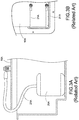
FIG. 2A and FIG. 2B , which show an assembled sectional view and an assembled top view of a first connection manner between aninductor 20A and acircuit board 10A of the related art, respectively. A connection manner between aninductor 20A and acircuit board 10A is shown inFIG. 2A and FIG. 2B . Theinductor 20A is electrically connected to thecircuit board 10A throughconnection wires 21A. In this connection manner, digging holes on thecircuit board 10A is necessary so that theconnection wires 21A can pass through thecircuit board 10A to be electrically connected to and locked on thecircuit board 10A. However, it would cause damage to theconnection wires 21A as well as increase process time. - Please refer to
FIG. 3A and FIG. 3B , which show an assembled sectional view and an assembled top view of a second connection manner between theinductor 20A and thecircuit board 10A of the related art, respectively. Another connection manner between theinductor 20A and thecircuit board 10A is shown inFIG. 3A and FIG. 3B . In comparison withFIG. 2A and FIG. 2B , theconnection wires 21A bypasses thecircuit board 10A to be electrically connected to and locked on thecircuit board 10A without digging holes on thecircuit board 10A. However, it would increase costs and power consumption due to the lengtheningconnection wires 21A. - Moreover, in the two connection manners, since the
connection wires 21A extend above thecircuit board 10A, the electromagnetic interference caused by the high-frequency current flowing through theconnection wires 21A to interfere circuit components mounted on thecircuit substrate 10A and reduce overall efficiency. - An objective of the present disclosure is to provide a connection structure of an inductive element to solve problems of increasing costs, power consumption, and electromagnetic interference due to the lengthening connection wires.
- In order to achieve the above-mentioned objective, the connection structure of the inductive element includes a circuit substrate, an inductive element, at least one connection wire, a supporting element, a containing element, a positioning element, a connecting element, and a locking element. The circuit substrate has a through hole. Each connection wire has a first end and a second end opposite to the first end. The first end is connected to the inductive element and a fixed terminal is disposed on the second end. The supporting element is disposed on a base body and provided to support the connection wire. The containing element is formed on the supporting element and provides a containing space. The positioning element is contained in the containing space, and the positioning element has a positioning part. The connecting element has a first connecting part and a second connecting part, and the first connecting part is connected to the positioning part to clip the fixed terminal. The locking element has a locking part, and the locking part is connected to the second connecting part to lock on the circuit substrate.
- Accordingly, the connection structure of the inductive element is provided to effectively and significantly reduce costs, power consumption, and electromagnetic interference.
- It is to be understood that both the foregoing general description and the following detailed description are exemplary, and are intended to provide further explanation of the present disclosure as claimed. Other advantages and features of the present disclosure will be apparent from the following description, drawings and claims.
- The present disclosure can be more fully understood by reading the following detailed description of the embodiment, with reference made to the accompanying drawings as follows:
-
FIG. 1 is a circuit block diagram of a grid-connected inverter system of the related art. -
FIG. 2A is an assembled sectional view of a first connection manner between an inductor and a circuit board of the related art. -
FIG. 2B is an assembled top view of the first connection manner between the inductor and the circuit board of the related art. -
FIG. 3A is an assembled sectional view of a second connection manner between the inductor and the circuit board of the related art. -
FIG. 3B is an assembled top view of the second connection manner between the inductor and the circuit board of the related art. -
FIG. 4 is a perspective exploded view of a connection structure of an inductive element according to a first embodiment of the present disclosure. -
FIG. 5 is an assembled sectional view of the connection structure of the inductive element according to a first embodiment of the present disclosure. -
FIG. 6 is an assembled sectional view of the connection structure of the inductive element disposed on a base body according to the first embodiment of the present disclosure. -
FIG. 7 is a partial perspective exploded view of the connection structure of the inductive element according to a second embodiment of the present disclosure. -
FIG. 8 is a partial perspective exploded view of the connection structure of the inductive element according to a third embodiment of the present disclosure. -
FIG. 9 is a partial perspective exploded view of the connection structure of the inductive element according to a fourth embodiment of the present disclosure. -
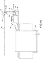
FIG. 10 is an assembled sectional view of the connection structure of the inductive element according to a fifth embodiment of the present disclosure. -
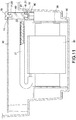
FIG. 11 is an assembled sectional view of the connection structure of the inductive element according to a sixth embodiment of the present disclosure. -
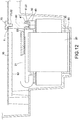
FIG. 12 is an assembled sectional view of the connection structure of the inductive element according to a seventh embodiment of the present disclosure. - Reference will now be made to the drawing figures to describe the present disclosure in detail. It will be understood that the drawing figures and exemplified embodiments of present disclosure are not limited to the details thereof.
- Please refer to
FIG. 4 andFIG. 5 , which show a perspective exploded view and an assembled sectional view of a connection structure of an inductive element according to a first embodiment of the present disclosure, respectively. The connection structure of the inductive element (hereinafter referred to as "connection structure") includes acircuit substrate 10, aninductive element 20, at least oneconnection wire 21, a supportingelement 30, a containingelement 40, apositioning element 50, a connectingelement 60, and a lockingelement 70. Thecircuit substrate 10 may be a printed circuit board (PCB) or other substrates capable of supporting circuit elements. Thecircuit substrate 10 has a throughhole 11 thereon. Theinductive element 20, such as an inductor which has a core and a coil wound on the core. In particular, the type of the core may be a U-shaped core, a block-shaped core, or others. - Each
connection wire 21 may be, for example but not limited to, a cable wire. More specifically, the at least oneconnection wire 21 may be connected to the coil through at least one connection pin (not shown) so that an output voltage and/or an output current of theinductive element 20 can be provided through the at least one connection pin. Theconnection wire 21 has two ends, i.e., a first end and a second end. The first end (also referred to as "connection end") is connected to a coil wound on the core of theinductive element 20, and a fixedterminal 22 is disposed on the second end (also referred to as "free end"). In different embodiments, the fixedterminal 22 may be a ring-shaped terminal, a C-shaped terminal, a U-shaped terminal, a V-shaped terminal, or so on. - Please refer to
FIG. 6 , which shows an assembled sectional view of the connection structure of the inductive element disposed on a base body according to the first embodiment of the present disclosure. The major difference betweenFIG. 6 andFIG. 5 is that abase body 90 is illustrated in the former. Thebase body 90 may be an inner base of a case, and the inner base may be made of non-conductive materials or conductive materials. Theinductive element 20, thecircuit substrate 10, and the above-mentioned elements are contained in the case. Also, thebase body 90 may be, for example but not limited to, formed by a die-casting manner. The supportingelement 30 is disposed on thebase body 90, namely the supportingelement 30 is disposed on the inner base of the case. Further, by injecting glue into an inner space of the case, theinductive element 20 can be firmly disposed on thebase body 90 and has good heat dissipation. - See
FIG. 4 andFIG. 5 again, the containingelement 40 is formed on the supportingelement 30 to provide a containingspace 41. In different embodiments, the supportingelement 30 is integrally or detachably formed with the containingelement 40. For example, the supportingelement 30 may be integrally with the containingelement 40 by an injection-molded manner or a die-casting manner so that the containingspace 41 is formed in the containingelement 40 and the containingelement 40 is formed on the supportingelement 30. Further, the supportingelement 30 and the containingelement 40 are two separable elements (i.e., two-piece construction), and the containingelement 40 is formed on the supportingelement 30 by connecting the two separable elements. - The
positioning element 50 is contained in the containingspace 41 of the containingelement 40, and thepositioning element 50 has apositioning part 51. As the embodiment shown inFIG. 4 , the containingelement 40 has a hexagonal cross section from top view, and the positioning element correspondingly has a hexagonal cross section from top view so that thepositioning element 50 can be contained in the containingspace 41 of the containingelement 40. In one embodiment, thepositioning element 50 is a hexagonal nut which can be a plastic nut or a metal nut. In other embodiments, thepositioning element 50 may be a nut with a polygonal cross section from top view or made of another material. Also, the containingelement 40 is designed corresponding to thepositioning element 50. - The connecting
element 60 has a first connectingpart 61 and a second connectingpart 62. As the embodiment shown inFIG. 4 andFIG. 5 , the first connectingpart 61 of the connectingelement 60 passes through the fixedterminal 22, which is a ring-shaped terminal, to connect to thepositioning part 51 of thepositioning element 50 so that the fixedterminal 22 is clipped between the first connectingpart 61 and thepositioning part 51. As the embodiment shown inFIG. 4 andFIG. 5 , the connectingelement 60 has a hexagonal cross section from top view, and the first connectingpart 61 with an external thread outwardly protrudes from one end of the connectingelement 60. Thepositioning part 51 of thepositioning element 50 is a concave structure. Take thepositioning element 50 as the hexagonal nut for example, thepositioning part 51 is an internal thread of the hexagonal nut. Accordingly, the first connectingpart 61 with the external thread passes through the fixedterminal 22 to connect to the internal thread, namely thepositioning part 51 of the hexagonal nut by a screw connection manner. When the first connectingpart 61 is screwed and fastened to thepositioning part 51, the fixedterminal 22 can be clipped between the first connectingpart 61 and thepositioning part 51. - The locking
element 70 has a lockingpart 71. As the embodiment shown inFIG. 4 , the lockingpart 71 of the lockingelement 70 passes through the throughhole 11 of thecircuit substrate 10 to connect to the second connectingpart 62 of the connectingelement 60 so that the lockingelement 70 locks on thecircuit substrate 10. As the embodiment shown inFIG. 4 andFIG. 5 , the second connectingpart 62 of the connectingelement 60 is a concave structure. Take the connectingelement 60 as a hexagonal column for example, the second connectingpart 62 is an internal thread of the hexagonal column. Also, the lockingpart 71 with an external thread outwardly protrudes from one end of the lockingelement 70. In this embodiment, the lockingelement 70 may be a screw. Accordingly, the lockingpart 71 with the external thread passes through the throughhole 11 of thecircuit substrate 10 to connect to the internal thread, namely the second connectingpart 62 of the hexagonal column by a screw connection manner. When the lockingpart 71 is screwed and fastened to the second connectingpart 62, thecircuit substrate 10 can be clipped between the lockingpart 71 and the second connectingpart 62, namely the lockingelement 70 locks on thecircuit substrate 10. - Please refer to
FIG. 7 ,FIG. 8 , andFIG. 9 , which show partial perspective exploded views of the connection structure of the inductive element according to a second embodiment, a third embodiment, and a fourth embodiment of the present disclosure, respectively. These embodiments show different connection designs between the positioningpart 51 and the first connectingpart 61 and between the lockingpart 71 and the second connectingpart 62. - As the second embodiment shown in
FIG. 7 , thepositioning part 51 of thepositioning element 50 is a concave structure, and therefore the first connectingpart 61 of the connectingelement 60 is correspondingly a convex structure. Moreover, the second connectingpart 62 of the connectingelement 60 is a convex structure, and therefore the lockingpart 71 of the lockingelement 70 is correspondingly a concave structure. - As the third embodiment shown in
FIG. 8 , thepositioning part 51 of thepositioning element 50 is a convex structure, and therefore the first connectingpart 61 of the connectingelement 60 is correspondingly a concave structure. Moreover, the second connectingpart 62 of the connectingelement 60 is a concave structure, and therefore the lockingpart 71 of the lockingelement 70 is correspondingly a convex structure. - As the fourth embodiment shown in
FIG. 9 , thepositioning part 51 of thepositioning element 50 is a convex structure, and therefore the first connectingpart 61 of the connectingelement 60 is correspondingly a concave structure. Moreover, the second connectingpart 62 of the connectingelement 60 is a convex structure, and therefore the lockingpart 71 of the lockingelement 70 is correspondingly a concave structure. - The four different connection designs between the positioning
part 51 and the first connectingpart 61 and between the lockingpart 71 and the second connectingpart 62 are not limited to implement by the hexagonal nut or the hexagonal column with the internal thread for the concave structure and to implement by the hexagonal column or the screw with the external thread for the convex structure. As long as a component which has connecting and/or locking functions, it would be used as thepositioning part 51, the first connectingpart 61, the second connectingpart 62, or the lockingpart 71, that is, the concave structure is not limited to be implemented by the nut with the internal thread and the convex structure is not limited to be implemented by the screw with the external thread. - Please refer to
FIG. 10 , which shows an assembled sectional view of the connection structure of the inductive element according to a fifth embodiment of the present disclosure. The major difference betweenFIG. 10 andFIG. 5 is that the position of theconnection wire 21 extending from theinductive element 20 is different. In the latter shown inFIG. 5 , theconnection wire 21 is extended from at one side, which is away from the positioning element 50 (or the connectingelement 60, the locking element 70) of theinductive element 20. From the view ofFIG. 5 , theconnection wire 21 is connected at a left side of theinductive element 20 and extended to thepositioning element 50. If the connection wire is not easily bent, the configuration shown inFIG. 5 is beneficial to reduce the distance between theinductive element 20 and the connecting element 60 (or the locking element 70), thereby saving the inner space of the case. In comparison withFIG. 5 , if the connection wire is easily bent, theconnection wire 21 shown inFIG. 10 is extended from at one side, which is near to the positioning element 50 (or the connectingelement 60, the locking element 70) of theinductive element 20. From the view ofFIG. 10 , theconnection wire 21 is connected at a right side of theinductive element 20 and extended to thepositioning element 50. Therefore, the configuration shown inFIG. 10 is beneficial to significantly shorten length and reduce costs of theconnection wire 21. - Please refer to
FIG. 11 , which shows an assembled sectional view of the connection structure of the inductive element according to a sixth embodiment of the present disclosure. The major difference betweenFIG. 11 andFIG. 6 is that the position of the supportingelement 30 corresponding to theinductive element 20 is different. In the latter shown inFIG. 6 , the supportingelement 30 is disposed in a space between the core and the coil, namely the supportingelement 30 is disposed inside theinductive element 20. In comparison withFIG. 6 , the supportingelement 30 is not disposed in the space between the core and the coil, namely the supportingelement 30 is disposed outside theinductive element 20. Moreover, the position of the supportingelement 30 is not limited to the above-mentioned embodiments, and therefore the position of the supportingelement 30 corresponding to theinductive element 20 may be adjusted according to the type of the core, the available space, or so on. Regardless of the U-shaped core or the block-shaped core, the connection relationship among thecircuit substrate 10, theinductive element 20, the supportingelement 30, the containingelement 40, thepositioning element 50, the connectingelement 60, and the lockingelement 70 can be implemented. - Please refer to
FIG. 12 , which shows an assembled sectional view of the connection structure of the inductive element according to a seventh embodiment of the present disclosure. In this embodiment, the connection structure further includes ametal plate 80. Themetal plate 80 is disposed between thecircuit substrate 10 and theconnection wire 21 for providing radiation shielding, thereby significantly reducing electromagnetic interference caused by the high-frequency current flowing through theconnection wire 21 to interfere circuit components mounted on thecircuit substrate 10. - In conclusion, the present disclosure has following features and advantages:
- 1. The connection structure of the inductive element is provided to shorten length of the connection wire, reduce required costs, and reduce power consumption.
- 2. The connection structure of the inductive element is provided to reduce electromagnetic interference and increase overall efficiency.
- 3. The positioning part, the first connecting part, the second connecting part, and the locking part can be concave structure or convex structure to increase design diversity and convenience of use.
- 4. The glue is injected into the inner space of the case to fix the inductive element and make the inductive element have good heat dissipation.
Claims (15)
- A connection structure of an inductive element, characterized in that the connection structure of the inductive element comprising:a circuit substrate (10) having a through hole (11);an inductive element (20) and at least one connection wire (21), and each connection wire (21) having a first end connected to the inductive element (20) and a second end being opposite to the first end and having a fixed terminal (22) disposed on the second end;a supporting element (30) disposed on a base body (90) and configured to support the connection wire (21);a containing element (40) formed on the supporting element (30) and configured to provide a containing space (41);a positioning element (50) contained in the containing space (41), and the positioning element (50) having a positioning part (51);a connecting element (60) having a first connecting part (61) and a second connecting part (62), and the first connecting part (61) connected to the positioning part (51) to clip the fixed terminal (22); anda locking element (70) having a locking part (71), and the locking part (71) connected to the second connecting part (62) to lock on the circuit substrate (10).
- The connection structure of the inductive element in claim 1, wherein the positioning part (51) is a concave structure, the first connecting part (61) is a convex structure, the second connecting part (62) is a concave structure, and the locking part (71) is a convex structure.
- The connection structure of the inductive element in claim 1, wherein the positioning part (51) is a concave structure, the first connecting part (61) is a convex structure, the second connecting part (62) is a convex structure, and the locking part (71) is a concave structure.
- The connection structure of the inductive element in claim 1, wherein the positioning part (51) is a convex structure, the first connecting part (61) is a concave structure, the second connecting part (62) is a concave structure, and the locking part (71) is a convex structure.
- The connection structure of the inductive element in claim 1, wherein the positioning part (51) is a convex structure, the first connecting part (61) is a concave structure, the second connecting part (62) is a convex structure, and the locking part (71) is a concave structure.
- The connection structure of the inductive element in claim 1, wherein the supporting element (30) is combined with the inductive element (20).
- The connection structure of the inductive element in claim 1, wherein the supporting element (30) is separated from the inductive element (20).
- The connection structure of the inductive element in claim 1, wherein the connection wire (21) is connected to one side, which is away from the positioning element (50), the connecting element (60), or the locking element (70), of the inductive element (20).
- The connection structure of the inductive element in claim 1, wherein the connection wire (21) is connected to one side, which is near to the positioning element (50), the connecting element (60), or the locking element (70), of the inductive element (20).
- The connection structure of the inductive element in claim 1, further comprising:
a metal plate (80) disposed between the circuit substrate (10) and the connection wire (21). - The connection structure of the inductive element in claim 1, wherein the fixed terminal (22) is a ring-shaped terminal, a C-shaped terminal, a U-shaped terminal, or a V-shaped terminal.
- The connection structure of the inductive element in claim 1, wherein the supporting element (30) is integrally or detachably formed with the containing element (40).
- The connection structure of the inductive element in claim 1, wherein the base body (90) is an inner base of a case, and a glue is injected into an inner space of the case to fix the inductive element (20).
- The connection structure of the inductive element in claim 2, wherein the positioning element (50) is a nut.
- The connection structure of the inductive element in claim 2, wherein the locking element (70) is a screw.
Applications Claiming Priority (1)
| Application Number | Priority Date | Filing Date | Title |
|---|---|---|---|
| CN201810542419.8A CN110556236A (en) | 2018-05-30 | 2018-05-30 | Connection structure of inductance element |
Publications (2)
| Publication Number | Publication Date |
|---|---|
| EP3576280A1 true EP3576280A1 (en) | 2019-12-04 |
| EP3576280B1 EP3576280B1 (en) | 2021-12-08 |
Family
ID=63762399
Family Applications (1)
| Application Number | Title | Priority Date | Filing Date |
|---|---|---|---|
| EP18198676.1A Active EP3576280B1 (en) | 2018-05-30 | 2018-10-04 | Connection structure of inductive element |
Country Status (4)
| Country | Link |
|---|---|
| US (2) | US11600422B2 (en) |
| EP (1) | EP3576280B1 (en) |
| JP (1) | JP6498831B1 (en) |
| CN (2) | CN117766277A (en) |
Cited By (2)
| Publication number | Priority date | Publication date | Assignee | Title |
|---|---|---|---|---|
| EP4271152A1 (en) * | 2022-04-27 | 2023-11-01 | FRONIUS INTERNATIONAL GmbH | Electronic assembly comprising at least one printed circuit board and external electronic components and inverter with such an electronic assembly |
| EP4422366A1 (en) * | 2023-02-23 | 2024-08-28 | Huawei Digital Power Technologies Co., Ltd. | Power converter |
Families Citing this family (5)
| Publication number | Priority date | Publication date | Assignee | Title |
|---|---|---|---|---|
| CN111210970B (en) | 2020-02-12 | 2022-09-27 | 台达电子企业管理(上海)有限公司 | Terminal and electronic equipment |
| CN114828393B (en) * | 2022-06-28 | 2022-09-13 | 锦浪科技股份有限公司 | Wiring and locking structure of main board wire |
| CN115295289A (en) * | 2022-07-13 | 2022-11-04 | 华为数字能源技术有限公司 | Element assembling device in electronic equipment and electronic equipment |
| EP4498772A1 (en) * | 2023-07-28 | 2025-01-29 | Siemens Aktiengesellschaft | Electronic power assembly with improved design |
| TWI903885B (en) * | 2024-11-25 | 2025-11-01 | 英業達股份有限公司 | Adapter device |
Citations (4)
| Publication number | Priority date | Publication date | Assignee | Title |
|---|---|---|---|---|
| JP2005273839A (en) * | 2004-03-26 | 2005-10-06 | Fuji Electric Fa Components & Systems Co Ltd | Mounting body |
| US20060040529A1 (en) * | 2004-08-20 | 2006-02-23 | Via Technologies, Inc. | Main board and fixing component thereof |
| JP2014072926A (en) * | 2012-09-27 | 2014-04-21 | Sanyo Electric Co Ltd | Electrical apparatus |
| EP3285555A1 (en) * | 2016-08-15 | 2018-02-21 | Delta Electronics Inc. | Connection structure of electronic components and circuit board |
Family Cites Families (8)
| Publication number | Priority date | Publication date | Assignee | Title |
|---|---|---|---|---|
| JPS565321Y2 (en) * | 1980-03-12 | 1981-02-05 | ||
| JPS59195721U (en) * | 1983-06-14 | 1984-12-26 | 三菱電機株式会社 | Connection device for electrical conductors |
| JPH1012292A (en) * | 1996-06-24 | 1998-01-16 | Yazaki Corp | control unit |
| US6011769A (en) * | 1996-07-04 | 2000-01-04 | Tdk Corporation | Optical information recording/reproducing apparatus with high frequency imposing circuit |
| JP2013225564A (en) * | 2012-04-20 | 2013-10-31 | Mitsubishi Electric Corp | Connection structure of reactor |
| CN107770960B (en) | 2016-08-15 | 2020-01-03 | 台达电子工业股份有限公司 | Connection structure of electronic element and circuit board |
| JP6774728B2 (en) * | 2016-09-09 | 2020-10-28 | 株式会社タムラ製作所 | Terminal block and reactor |
| JP2024072926A (en) * | 2022-11-17 | 2024-05-29 | 日本電信電話株式会社 | Apparatus and method for searching minimum value of energy function, and program |
-
2018
- 2018-05-30 CN CN202311838348.3A patent/CN117766277A/en active Pending
- 2018-05-30 CN CN201810542419.8A patent/CN110556236A/en active Pending
- 2018-09-28 JP JP2018185143A patent/JP6498831B1/en active Active
- 2018-09-28 US US16/145,894 patent/US11600422B2/en active Active
- 2018-10-04 EP EP18198676.1A patent/EP3576280B1/en active Active
-
2023
- 2023-01-18 US US18/156,203 patent/US20230154664A1/en active Pending
Patent Citations (4)
| Publication number | Priority date | Publication date | Assignee | Title |
|---|---|---|---|---|
| JP2005273839A (en) * | 2004-03-26 | 2005-10-06 | Fuji Electric Fa Components & Systems Co Ltd | Mounting body |
| US20060040529A1 (en) * | 2004-08-20 | 2006-02-23 | Via Technologies, Inc. | Main board and fixing component thereof |
| JP2014072926A (en) * | 2012-09-27 | 2014-04-21 | Sanyo Electric Co Ltd | Electrical apparatus |
| EP3285555A1 (en) * | 2016-08-15 | 2018-02-21 | Delta Electronics Inc. | Connection structure of electronic components and circuit board |
Cited By (4)
| Publication number | Priority date | Publication date | Assignee | Title |
|---|---|---|---|---|
| EP4271152A1 (en) * | 2022-04-27 | 2023-11-01 | FRONIUS INTERNATIONAL GmbH | Electronic assembly comprising at least one printed circuit board and external electronic components and inverter with such an electronic assembly |
| WO2023208977A1 (en) * | 2022-04-27 | 2023-11-02 | Fronius International Gmbh | Electronic assembly comprising at least one circuit board and external electronic components, and inverter comprising such an electronic assembly |
| US12289854B2 (en) | 2022-04-27 | 2025-04-29 | Fronius International Gmbh | Electronic assembly comprising at least one circuit board and external electronic components, and inverter comprising such an electronic assembly |
| EP4422366A1 (en) * | 2023-02-23 | 2024-08-28 | Huawei Digital Power Technologies Co., Ltd. | Power converter |
Also Published As
| Publication number | Publication date |
|---|---|
| US11600422B2 (en) | 2023-03-07 |
| CN110556236A (en) | 2019-12-10 |
| US20190371509A1 (en) | 2019-12-05 |
| CN117766277A (en) | 2024-03-26 |
| EP3576280B1 (en) | 2021-12-08 |
| JP2019212886A (en) | 2019-12-12 |
| US20230154664A1 (en) | 2023-05-18 |
| JP6498831B1 (en) | 2019-04-10 |
Similar Documents
| Publication | Publication Date | Title |
|---|---|---|
| US20230154664A1 (en) | Connection structure of inductive element | |
| US9263177B1 (en) | Pin inductors and associated systems and methods | |
| EP1760867B1 (en) | Switching power supply unit | |
| US8164406B2 (en) | Transformer | |
| CN101840765B (en) | Coil component, transformer and switching power supply unit | |
| US20060279394A1 (en) | Terminal system for planar magnetics assembly | |
| US20200111599A1 (en) | Inductor and power supply conversion circuit | |
| CN101651024A (en) | High power manufacturing friendly transformer | |
| US7911309B2 (en) | Conductive winding module and transformer having such conductive winding module | |
| CN114499156A (en) | Integrated electromagnetic interference filter | |
| KR20220098116A (en) | Dc-dc converter | |
| CN101523684B (en) | Snap-on high-power, high-current connectors with integrated EMI filtering | |
| JP2018143010A (en) | Electronic circuit device | |
| CN114694927B (en) | Power conversion module | |
| CN109546450A (en) | Electric connector combination and its fixing seat | |
| CN219760020U (en) | Photovoltaic inverter | |
| EP3905500A1 (en) | In-vehicle power conversion device | |
| KR20140004847A (en) | Bobbin structure provided with terminal block and magnetic body using the same | |
| TWI660381B (en) | Connection structure of inductive element | |
| CN222952920U (en) | High-voltage high-power coupling inductor | |
| JP2006202895A (en) | Mounting structure of sheet metal wiring | |
| CN220234468U (en) | Inverter | |
| CN222421604U (en) | High Current Chip Inductor | |
| US10881024B2 (en) | Electronic device having a hermetically sealed housing with internal projection | |
| JP7853390B2 (en) | Inverters and cable-free inductors |
Legal Events
| Date | Code | Title | Description |
|---|---|---|---|
| PUAI | Public reference made under article 153(3) epc to a published international application that has entered the european phase |
Free format text: ORIGINAL CODE: 0009012 |
|
| STAA | Information on the status of an ep patent application or granted ep patent |
Free format text: STATUS: THE APPLICATION HAS BEEN PUBLISHED |
|
| AK | Designated contracting states |
Kind code of ref document: A1 Designated state(s): AL AT BE BG CH CY CZ DE DK EE ES FI FR GB GR HR HU IE IS IT LI LT LU LV MC MK MT NL NO PL PT RO RS SE SI SK SM TR |
|
| AX | Request for extension of the european patent |
Extension state: BA ME |
|
| STAA | Information on the status of an ep patent application or granted ep patent |
Free format text: STATUS: REQUEST FOR EXAMINATION WAS MADE |
|
| 17P | Request for examination filed |
Effective date: 20200604 |
|
| RBV | Designated contracting states (corrected) |
Designated state(s): AL AT BE BG CH CY CZ DE DK EE ES FI FR GB GR HR HU IE IS IT LI LT LU LV MC MK MT NL NO PL PT RO RS SE SI SK SM TR |
|
| STAA | Information on the status of an ep patent application or granted ep patent |
Free format text: STATUS: EXAMINATION IS IN PROGRESS |
|
| 17Q | First examination report despatched |
Effective date: 20200930 |
|
| GRAP | Despatch of communication of intention to grant a patent |
Free format text: ORIGINAL CODE: EPIDOSNIGR1 |
|
| STAA | Information on the status of an ep patent application or granted ep patent |
Free format text: STATUS: GRANT OF PATENT IS INTENDED |
|
| INTG | Intention to grant announced |
Effective date: 20210621 |
|
| GRAS | Grant fee paid |
Free format text: ORIGINAL CODE: EPIDOSNIGR3 |
|
| GRAA | (expected) grant |
Free format text: ORIGINAL CODE: 0009210 |
|
| STAA | Information on the status of an ep patent application or granted ep patent |
Free format text: STATUS: THE PATENT HAS BEEN GRANTED |
|
| AK | Designated contracting states |
Kind code of ref document: B1 Designated state(s): AL AT BE BG CH CY CZ DE DK EE ES FI FR GB GR HR HU IE IS IT LI LT LU LV MC MK MT NL NO PL PT RO RS SE SI SK SM TR |
|
| REG | Reference to a national code |
Ref country code: GB Ref legal event code: FG4D |
|
| REG | Reference to a national code |
Ref country code: AT Ref legal event code: REF Ref document number: 1454500 Country of ref document: AT Kind code of ref document: T Effective date: 20211215 Ref country code: CH Ref legal event code: EP |
|
| REG | Reference to a national code |
Ref country code: DE Ref legal event code: R096 Ref document number: 602018027802 Country of ref document: DE |
|
| REG | Reference to a national code |
Ref country code: IE Ref legal event code: FG4D |
|
| REG | Reference to a national code |
Ref country code: NL Ref legal event code: FP |
|
| REG | Reference to a national code |
Ref country code: LT Ref legal event code: MG9D |
|
| PG25 | Lapsed in a contracting state [announced via postgrant information from national office to epo] |
Ref country code: RS Free format text: LAPSE BECAUSE OF FAILURE TO SUBMIT A TRANSLATION OF THE DESCRIPTION OR TO PAY THE FEE WITHIN THE PRESCRIBED TIME-LIMIT Effective date: 20211208 Ref country code: LT Free format text: LAPSE BECAUSE OF FAILURE TO SUBMIT A TRANSLATION OF THE DESCRIPTION OR TO PAY THE FEE WITHIN THE PRESCRIBED TIME-LIMIT Effective date: 20211208 Ref country code: FI Free format text: LAPSE BECAUSE OF FAILURE TO SUBMIT A TRANSLATION OF THE DESCRIPTION OR TO PAY THE FEE WITHIN THE PRESCRIBED TIME-LIMIT Effective date: 20211208 Ref country code: BG Free format text: LAPSE BECAUSE OF FAILURE TO SUBMIT A TRANSLATION OF THE DESCRIPTION OR TO PAY THE FEE WITHIN THE PRESCRIBED TIME-LIMIT Effective date: 20220308 |
|
| REG | Reference to a national code |
Ref country code: AT Ref legal event code: MK05 Ref document number: 1454500 Country of ref document: AT Kind code of ref document: T Effective date: 20211208 |
|
| PG25 | Lapsed in a contracting state [announced via postgrant information from national office to epo] |
Ref country code: SE Free format text: LAPSE BECAUSE OF FAILURE TO SUBMIT A TRANSLATION OF THE DESCRIPTION OR TO PAY THE FEE WITHIN THE PRESCRIBED TIME-LIMIT Effective date: 20211208 Ref country code: NO Free format text: LAPSE BECAUSE OF FAILURE TO SUBMIT A TRANSLATION OF THE DESCRIPTION OR TO PAY THE FEE WITHIN THE PRESCRIBED TIME-LIMIT Effective date: 20220308 Ref country code: LV Free format text: LAPSE BECAUSE OF FAILURE TO SUBMIT A TRANSLATION OF THE DESCRIPTION OR TO PAY THE FEE WITHIN THE PRESCRIBED TIME-LIMIT Effective date: 20211208 Ref country code: HR Free format text: LAPSE BECAUSE OF FAILURE TO SUBMIT A TRANSLATION OF THE DESCRIPTION OR TO PAY THE FEE WITHIN THE PRESCRIBED TIME-LIMIT Effective date: 20211208 Ref country code: GR Free format text: LAPSE BECAUSE OF FAILURE TO SUBMIT A TRANSLATION OF THE DESCRIPTION OR TO PAY THE FEE WITHIN THE PRESCRIBED TIME-LIMIT Effective date: 20220309 Ref country code: ES Free format text: LAPSE BECAUSE OF FAILURE TO SUBMIT A TRANSLATION OF THE DESCRIPTION OR TO PAY THE FEE WITHIN THE PRESCRIBED TIME-LIMIT Effective date: 20211208 |
|
| PG25 | Lapsed in a contracting state [announced via postgrant information from national office to epo] |
Ref country code: SM Free format text: LAPSE BECAUSE OF FAILURE TO SUBMIT A TRANSLATION OF THE DESCRIPTION OR TO PAY THE FEE WITHIN THE PRESCRIBED TIME-LIMIT Effective date: 20211208 Ref country code: SK Free format text: LAPSE BECAUSE OF FAILURE TO SUBMIT A TRANSLATION OF THE DESCRIPTION OR TO PAY THE FEE WITHIN THE PRESCRIBED TIME-LIMIT Effective date: 20211208 Ref country code: RO Free format text: LAPSE BECAUSE OF FAILURE TO SUBMIT A TRANSLATION OF THE DESCRIPTION OR TO PAY THE FEE WITHIN THE PRESCRIBED TIME-LIMIT Effective date: 20211208 Ref country code: PT Free format text: LAPSE BECAUSE OF FAILURE TO SUBMIT A TRANSLATION OF THE DESCRIPTION OR TO PAY THE FEE WITHIN THE PRESCRIBED TIME-LIMIT Effective date: 20220408 Ref country code: EE Free format text: LAPSE BECAUSE OF FAILURE TO SUBMIT A TRANSLATION OF THE DESCRIPTION OR TO PAY THE FEE WITHIN THE PRESCRIBED TIME-LIMIT Effective date: 20211208 Ref country code: CZ Free format text: LAPSE BECAUSE OF FAILURE TO SUBMIT A TRANSLATION OF THE DESCRIPTION OR TO PAY THE FEE WITHIN THE PRESCRIBED TIME-LIMIT Effective date: 20211208 |
|
| PG25 | Lapsed in a contracting state [announced via postgrant information from national office to epo] |
Ref country code: PL Free format text: LAPSE BECAUSE OF FAILURE TO SUBMIT A TRANSLATION OF THE DESCRIPTION OR TO PAY THE FEE WITHIN THE PRESCRIBED TIME-LIMIT Effective date: 20211208 Ref country code: AT Free format text: LAPSE BECAUSE OF FAILURE TO SUBMIT A TRANSLATION OF THE DESCRIPTION OR TO PAY THE FEE WITHIN THE PRESCRIBED TIME-LIMIT Effective date: 20211208 |
|
| REG | Reference to a national code |
Ref country code: DE Ref legal event code: R097 Ref document number: 602018027802 Country of ref document: DE |
|
| PG25 | Lapsed in a contracting state [announced via postgrant information from national office to epo] |
Ref country code: IS Free format text: LAPSE BECAUSE OF FAILURE TO SUBMIT A TRANSLATION OF THE DESCRIPTION OR TO PAY THE FEE WITHIN THE PRESCRIBED TIME-LIMIT Effective date: 20220408 |
|
| PLBE | No opposition filed within time limit |
Free format text: ORIGINAL CODE: 0009261 |
|
| STAA | Information on the status of an ep patent application or granted ep patent |
Free format text: STATUS: NO OPPOSITION FILED WITHIN TIME LIMIT |
|
| PG25 | Lapsed in a contracting state [announced via postgrant information from national office to epo] |
Ref country code: DK Free format text: LAPSE BECAUSE OF FAILURE TO SUBMIT A TRANSLATION OF THE DESCRIPTION OR TO PAY THE FEE WITHIN THE PRESCRIBED TIME-LIMIT Effective date: 20211208 Ref country code: AL Free format text: LAPSE BECAUSE OF FAILURE TO SUBMIT A TRANSLATION OF THE DESCRIPTION OR TO PAY THE FEE WITHIN THE PRESCRIBED TIME-LIMIT Effective date: 20211208 |
|
| 26N | No opposition filed |
Effective date: 20220909 |
|
| PG25 | Lapsed in a contracting state [announced via postgrant information from national office to epo] |
Ref country code: SI Free format text: LAPSE BECAUSE OF FAILURE TO SUBMIT A TRANSLATION OF THE DESCRIPTION OR TO PAY THE FEE WITHIN THE PRESCRIBED TIME-LIMIT Effective date: 20211208 |
|
| PG25 | Lapsed in a contracting state [announced via postgrant information from national office to epo] |
Ref country code: MC Free format text: LAPSE BECAUSE OF FAILURE TO SUBMIT A TRANSLATION OF THE DESCRIPTION OR TO PAY THE FEE WITHIN THE PRESCRIBED TIME-LIMIT Effective date: 20211208 |
|
| REG | Reference to a national code |
Ref country code: CH Ref legal event code: PL |
|
| REG | Reference to a national code |
Ref country code: BE Ref legal event code: MM Effective date: 20221031 |
|
| PG25 | Lapsed in a contracting state [announced via postgrant information from national office to epo] |
Ref country code: LU Free format text: LAPSE BECAUSE OF NON-PAYMENT OF DUE FEES Effective date: 20221004 |
|
| PG25 | Lapsed in a contracting state [announced via postgrant information from national office to epo] |
Ref country code: LI Free format text: LAPSE BECAUSE OF NON-PAYMENT OF DUE FEES Effective date: 20221031 Ref country code: CH Free format text: LAPSE BECAUSE OF NON-PAYMENT OF DUE FEES Effective date: 20221031 |
|
| PG25 | Lapsed in a contracting state [announced via postgrant information from national office to epo] |
Ref country code: BE Free format text: LAPSE BECAUSE OF NON-PAYMENT OF DUE FEES Effective date: 20221031 |
|
| PG25 | Lapsed in a contracting state [announced via postgrant information from national office to epo] |
Ref country code: IE Free format text: LAPSE BECAUSE OF NON-PAYMENT OF DUE FEES Effective date: 20221004 |
|
| PG25 | Lapsed in a contracting state [announced via postgrant information from national office to epo] |
Ref country code: HU Free format text: LAPSE BECAUSE OF FAILURE TO SUBMIT A TRANSLATION OF THE DESCRIPTION OR TO PAY THE FEE WITHIN THE PRESCRIBED TIME-LIMIT; INVALID AB INITIO Effective date: 20181004 |
|
| PG25 | Lapsed in a contracting state [announced via postgrant information from national office to epo] |
Ref country code: CY Free format text: LAPSE BECAUSE OF FAILURE TO SUBMIT A TRANSLATION OF THE DESCRIPTION OR TO PAY THE FEE WITHIN THE PRESCRIBED TIME-LIMIT Effective date: 20211208 |
|
| PG25 | Lapsed in a contracting state [announced via postgrant information from national office to epo] |
Ref country code: MK Free format text: LAPSE BECAUSE OF FAILURE TO SUBMIT A TRANSLATION OF THE DESCRIPTION OR TO PAY THE FEE WITHIN THE PRESCRIBED TIME-LIMIT Effective date: 20211208 |
|
| PG25 | Lapsed in a contracting state [announced via postgrant information from national office to epo] |
Ref country code: TR Free format text: LAPSE BECAUSE OF FAILURE TO SUBMIT A TRANSLATION OF THE DESCRIPTION OR TO PAY THE FEE WITHIN THE PRESCRIBED TIME-LIMIT Effective date: 20211208 |
|
| PG25 | Lapsed in a contracting state [announced via postgrant information from national office to epo] |
Ref country code: MT Free format text: LAPSE BECAUSE OF FAILURE TO SUBMIT A TRANSLATION OF THE DESCRIPTION OR TO PAY THE FEE WITHIN THE PRESCRIBED TIME-LIMIT Effective date: 20211208 |
|
| PGFP | Annual fee paid to national office [announced via postgrant information from national office to epo] |
Ref country code: NL Payment date: 20251026 Year of fee payment: 8 |
|
| PGFP | Annual fee paid to national office [announced via postgrant information from national office to epo] |
Ref country code: DE Payment date: 20251029 Year of fee payment: 8 |
|
| PGFP | Annual fee paid to national office [announced via postgrant information from national office to epo] |
Ref country code: GB Payment date: 20251027 Year of fee payment: 8 |
|
| PGFP | Annual fee paid to national office [announced via postgrant information from national office to epo] |
Ref country code: IT Payment date: 20251021 Year of fee payment: 8 |
|
| PGFP | Annual fee paid to national office [announced via postgrant information from national office to epo] |
Ref country code: FR Payment date: 20251027 Year of fee payment: 8 |