EP3576277B1 - Method for controlling a psfb converter and psfb converter - Google Patents
Method for controlling a psfb converter and psfb converter Download PDFInfo
- Publication number
- EP3576277B1 EP3576277B1 EP19177639.2A EP19177639A EP3576277B1 EP 3576277 B1 EP3576277 B1 EP 3576277B1 EP 19177639 A EP19177639 A EP 19177639A EP 3576277 B1 EP3576277 B1 EP 3576277B1
- Authority
- EP
- European Patent Office
- Prior art keywords
- drive signal
- clock
- bridge arm
- mosfet
- phase difference
- Prior art date
- Legal status (The legal status is an assumption and is not a legal conclusion. Google has not performed a legal analysis and makes no representation as to the accuracy of the status listed.)
- Active
Links
Images



Classifications
-
- H—ELECTRICITY
- H02—GENERATION; CONVERSION OR DISTRIBUTION OF ELECTRIC POWER
- H02M—APPARATUS FOR CONVERSION BETWEEN AC AND AC, BETWEEN AC AND DC, OR BETWEEN DC AND DC, AND FOR USE WITH MAINS OR SIMILAR POWER SUPPLY SYSTEMS; CONVERSION OF DC OR AC INPUT POWER INTO SURGE OUTPUT POWER; CONTROL OR REGULATION THEREOF
- H02M3/00—Conversion of DC power input into DC power output
- H02M3/22—Conversion of DC power input into DC power output with intermediate conversion into AC
- H02M3/24—Conversion of DC power input into DC power output with intermediate conversion into AC by static converters
- H02M3/28—Conversion of DC power input into DC power output with intermediate conversion into AC by static converters using discharge tubes with control electrode or semiconductor devices with control electrode to produce the intermediate AC
- H02M3/325—Conversion of DC power input into DC power output with intermediate conversion into AC by static converters using discharge tubes with control electrode or semiconductor devices with control electrode to produce the intermediate AC using devices of a triode or a transistor type requiring continuous application of a control signal
- H02M3/335—Conversion of DC power input into DC power output with intermediate conversion into AC by static converters using discharge tubes with control electrode or semiconductor devices with control electrode to produce the intermediate AC using devices of a triode or a transistor type requiring continuous application of a control signal using semiconductor devices only
- H02M3/337—Conversion of DC power input into DC power output with intermediate conversion into AC by static converters using discharge tubes with control electrode or semiconductor devices with control electrode to produce the intermediate AC using devices of a triode or a transistor type requiring continuous application of a control signal using semiconductor devices only in push-pull configuration
- H02M3/3376—Conversion of DC power input into DC power output with intermediate conversion into AC by static converters using discharge tubes with control electrode or semiconductor devices with control electrode to produce the intermediate AC using devices of a triode or a transistor type requiring continuous application of a control signal using semiconductor devices only in push-pull configuration with automatic control of output voltage or current
-
- H—ELECTRICITY
- H02—GENERATION; CONVERSION OR DISTRIBUTION OF ELECTRIC POWER
- H02M—APPARATUS FOR CONVERSION BETWEEN AC AND AC, BETWEEN AC AND DC, OR BETWEEN DC AND DC, AND FOR USE WITH MAINS OR SIMILAR POWER SUPPLY SYSTEMS; CONVERSION OF DC OR AC INPUT POWER INTO SURGE OUTPUT POWER; CONTROL OR REGULATION THEREOF
- H02M3/00—Conversion of DC power input into DC power output
- H02M3/02—Conversion of DC power input into DC power output without intermediate conversion into AC
- H02M3/04—Conversion of DC power input into DC power output without intermediate conversion into AC by static converters
- H02M3/10—Conversion of DC power input into DC power output without intermediate conversion into AC by static converters using discharge tubes with control electrode or semiconductor devices with control electrode
- H02M3/145—Conversion of DC power input into DC power output without intermediate conversion into AC by static converters using discharge tubes with control electrode or semiconductor devices with control electrode using devices of a triode or transistor type requiring continuous application of a control signal
- H02M3/155—Conversion of DC power input into DC power output without intermediate conversion into AC by static converters using discharge tubes with control electrode or semiconductor devices with control electrode using devices of a triode or transistor type requiring continuous application of a control signal using semiconductor devices only
- H02M3/156—Conversion of DC power input into DC power output without intermediate conversion into AC by static converters using discharge tubes with control electrode or semiconductor devices with control electrode using devices of a triode or transistor type requiring continuous application of a control signal using semiconductor devices only with automatic control of output voltage or current, e.g. switching regulators
- H02M3/158—Conversion of DC power input into DC power output without intermediate conversion into AC by static converters using discharge tubes with control electrode or semiconductor devices with control electrode using devices of a triode or transistor type requiring continuous application of a control signal using semiconductor devices only with automatic control of output voltage or current, e.g. switching regulators including plural semiconductor devices as final control devices for a single load
- H02M3/1584—Conversion of DC power input into DC power output without intermediate conversion into AC by static converters using discharge tubes with control electrode or semiconductor devices with control electrode using devices of a triode or transistor type requiring continuous application of a control signal using semiconductor devices only with automatic control of output voltage or current, e.g. switching regulators including plural semiconductor devices as final control devices for a single load with a plurality of power processing stages connected in parallel
-
- H—ELECTRICITY
- H02—GENERATION; CONVERSION OR DISTRIBUTION OF ELECTRIC POWER
- H02M—APPARATUS FOR CONVERSION BETWEEN AC AND AC, BETWEEN AC AND DC, OR BETWEEN DC AND DC, AND FOR USE WITH MAINS OR SIMILAR POWER SUPPLY SYSTEMS; CONVERSION OF DC OR AC INPUT POWER INTO SURGE OUTPUT POWER; CONTROL OR REGULATION THEREOF
- H02M3/00—Conversion of DC power input into DC power output
- H02M3/22—Conversion of DC power input into DC power output with intermediate conversion into AC
- H02M3/24—Conversion of DC power input into DC power output with intermediate conversion into AC by static converters
- H02M3/28—Conversion of DC power input into DC power output with intermediate conversion into AC by static converters using discharge tubes with control electrode or semiconductor devices with control electrode to produce the intermediate AC
- H02M3/325—Conversion of DC power input into DC power output with intermediate conversion into AC by static converters using discharge tubes with control electrode or semiconductor devices with control electrode to produce the intermediate AC using devices of a triode or a transistor type requiring continuous application of a control signal
- H02M3/335—Conversion of DC power input into DC power output with intermediate conversion into AC by static converters using discharge tubes with control electrode or semiconductor devices with control electrode to produce the intermediate AC using devices of a triode or a transistor type requiring continuous application of a control signal using semiconductor devices only
- H02M3/33507—Conversion of DC power input into DC power output with intermediate conversion into AC by static converters using discharge tubes with control electrode or semiconductor devices with control electrode to produce the intermediate AC using devices of a triode or a transistor type requiring continuous application of a control signal using semiconductor devices only with automatic control of the output voltage or current, e.g. flyback converters
- H02M3/33515—Conversion of DC power input into DC power output with intermediate conversion into AC by static converters using discharge tubes with control electrode or semiconductor devices with control electrode to produce the intermediate AC using devices of a triode or a transistor type requiring continuous application of a control signal using semiconductor devices only with automatic control of the output voltage or current, e.g. flyback converters with digital control
-
- H—ELECTRICITY
- H02—GENERATION; CONVERSION OR DISTRIBUTION OF ELECTRIC POWER
- H02M—APPARATUS FOR CONVERSION BETWEEN AC AND AC, BETWEEN AC AND DC, OR BETWEEN DC AND DC, AND FOR USE WITH MAINS OR SIMILAR POWER SUPPLY SYSTEMS; CONVERSION OF DC OR AC INPUT POWER INTO SURGE OUTPUT POWER; CONTROL OR REGULATION THEREOF
- H02M3/00—Conversion of DC power input into DC power output
- H02M3/22—Conversion of DC power input into DC power output with intermediate conversion into AC
- H02M3/24—Conversion of DC power input into DC power output with intermediate conversion into AC by static converters
- H02M3/28—Conversion of DC power input into DC power output with intermediate conversion into AC by static converters using discharge tubes with control electrode or semiconductor devices with control electrode to produce the intermediate AC
- H02M3/325—Conversion of DC power input into DC power output with intermediate conversion into AC by static converters using discharge tubes with control electrode or semiconductor devices with control electrode to produce the intermediate AC using devices of a triode or a transistor type requiring continuous application of a control signal
- H02M3/335—Conversion of DC power input into DC power output with intermediate conversion into AC by static converters using discharge tubes with control electrode or semiconductor devices with control electrode to produce the intermediate AC using devices of a triode or a transistor type requiring continuous application of a control signal using semiconductor devices only
- H02M3/33569—Conversion of DC power input into DC power output with intermediate conversion into AC by static converters using discharge tubes with control electrode or semiconductor devices with control electrode to produce the intermediate AC using devices of a triode or a transistor type requiring continuous application of a control signal using semiconductor devices only having several active switching elements
- H02M3/33573—Full-bridge at primary side of an isolation transformer
-
- H—ELECTRICITY
- H02—GENERATION; CONVERSION OR DISTRIBUTION OF ELECTRIC POWER
- H02M—APPARATUS FOR CONVERSION BETWEEN AC AND AC, BETWEEN AC AND DC, OR BETWEEN DC AND DC, AND FOR USE WITH MAINS OR SIMILAR POWER SUPPLY SYSTEMS; CONVERSION OF DC OR AC INPUT POWER INTO SURGE OUTPUT POWER; CONTROL OR REGULATION THEREOF
- H02M1/00—Details of apparatus for conversion
- H02M1/0003—Details of control, feedback or regulation circuits
-
- H—ELECTRICITY
- H02—GENERATION; CONVERSION OR DISTRIBUTION OF ELECTRIC POWER
- H02M—APPARATUS FOR CONVERSION BETWEEN AC AND AC, BETWEEN AC AND DC, OR BETWEEN DC AND DC, AND FOR USE WITH MAINS OR SIMILAR POWER SUPPLY SYSTEMS; CONVERSION OF DC OR AC INPUT POWER INTO SURGE OUTPUT POWER; CONTROL OR REGULATION THEREOF
- H02M1/00—Details of apparatus for conversion
- H02M1/0003—Details of control, feedback or regulation circuits
- H02M1/0006—Arrangements for supplying an adequate voltage to the control circuit of converters
-
- H—ELECTRICITY
- H02—GENERATION; CONVERSION OR DISTRIBUTION OF ELECTRIC POWER
- H02M—APPARATUS FOR CONVERSION BETWEEN AC AND AC, BETWEEN AC AND DC, OR BETWEEN DC AND DC, AND FOR USE WITH MAINS OR SIMILAR POWER SUPPLY SYSTEMS; CONVERSION OF DC OR AC INPUT POWER INTO SURGE OUTPUT POWER; CONTROL OR REGULATION THEREOF
- H02M1/00—Details of apparatus for conversion
- H02M1/0048—Circuits or arrangements for reducing losses
- H02M1/0054—Transistor switching losses
-
- H—ELECTRICITY
- H02—GENERATION; CONVERSION OR DISTRIBUTION OF ELECTRIC POWER
- H02M—APPARATUS FOR CONVERSION BETWEEN AC AND AC, BETWEEN AC AND DC, OR BETWEEN DC AND DC, AND FOR USE WITH MAINS OR SIMILAR POWER SUPPLY SYSTEMS; CONVERSION OF DC OR AC INPUT POWER INTO SURGE OUTPUT POWER; CONTROL OR REGULATION THEREOF
- H02M3/00—Conversion of DC power input into DC power output
- H02M3/01—Resonant DC/DC converters
-
- H—ELECTRICITY
- H02—GENERATION; CONVERSION OR DISTRIBUTION OF ELECTRIC POWER
- H02M—APPARATUS FOR CONVERSION BETWEEN AC AND AC, BETWEEN AC AND DC, OR BETWEEN DC AND DC, AND FOR USE WITH MAINS OR SIMILAR POWER SUPPLY SYSTEMS; CONVERSION OF DC OR AC INPUT POWER INTO SURGE OUTPUT POWER; CONTROL OR REGULATION THEREOF
- H02M7/00—Conversion of AC power input into DC power output; Conversion of DC power input into AC power output
- H02M7/42—Conversion of DC power input into AC power output without possibility of reversal
- H02M7/44—Conversion of DC power input into AC power output without possibility of reversal by static converters
- H02M7/48—Conversion of DC power input into AC power output without possibility of reversal by static converters using discharge tubes with control electrode or semiconductor devices with control electrode
- H02M7/53—Conversion of DC power input into AC power output without possibility of reversal by static converters using discharge tubes with control electrode or semiconductor devices with control electrode using devices of a triode or transistor type requiring continuous application of a control signal
- H02M7/537—Conversion of DC power input into AC power output without possibility of reversal by static converters using discharge tubes with control electrode or semiconductor devices with control electrode using devices of a triode or transistor type requiring continuous application of a control signal using semiconductor devices only, e.g. single switched pulse inverters
- H02M7/5387—Conversion of DC power input into AC power output without possibility of reversal by static converters using discharge tubes with control electrode or semiconductor devices with control electrode using devices of a triode or transistor type requiring continuous application of a control signal using semiconductor devices only, e.g. single switched pulse inverters in a bridge configuration
- H02M7/53871—Conversion of DC power input into AC power output without possibility of reversal by static converters using discharge tubes with control electrode or semiconductor devices with control electrode using devices of a triode or transistor type requiring continuous application of a control signal using semiconductor devices only, e.g. single switched pulse inverters in a bridge configuration with automatic control of output voltage or current
- H02M7/53878—Conversion of DC power input into AC power output without possibility of reversal by static converters using discharge tubes with control electrode or semiconductor devices with control electrode using devices of a triode or transistor type requiring continuous application of a control signal using semiconductor devices only, e.g. single switched pulse inverters in a bridge configuration with automatic control of output voltage or current by time shifting switching signals of one diagonal pair of the bridge with respect to the other diagonal pair
Definitions
- This application relates to the field of power supply technologies, and in particular, to a phase-shifted full bridge (PSFB) converter control method and a PSFB converter.
- PSFB phase-shifted full bridge
- a PSFB converter is capable of converting direct current into direct current of different voltages (for example, direct current of a lower voltage). Reliability of the PSFB converter needs to be improved.
- US2014/0177281 A1 discloses a full bridge converter in a power converting system and including a PSFB power converting system with a controller unit that is configured to balance the temperature of the legs of the converter.
- EP 1679783 A2 discloses a single stage switch mode power converter that receives a supply line voltage and a supply line current from a power supply line, and provides one or more regulated output voltages for a load, such as an amplifier.
- CN 103595274 A discloses a method for controlling a double-direction power flow high-frequency isolated active clamping rectifier.
- US 2014/092634 A1 discloses a mixed control method for a resonant converter, a resonant converter system and a mixed controller.
- CN 107070241 A discloses a method for controlling a PSFB
- This application provides a method for controlling a PSFB converter and a PSFB converter, to improve reliability of the PSFB converter.
- the technical solutions are as follows.
- a method for controlling a PSFB converter includes: controlling, by a control circuit, a first clock and a second clock to operate in a first state, and controlling a timer to start timing, where the PSFB converter includes a first bridge arm and a second bridge arm, the first bridge arm includes a first metal oxide semiconductor field effect transistor (MOSFET) and a second MOSFET, the second bridge arm includes a third MOSFET and a fourth MOSFET, a first drive signal output by the control circuit based on the first clock is input to a gate of the first MOSFET, a second drive signal output by the control circuit based on the first clock is input to a gate of the second MOSFET, a third drive signal output by the control circuit based on the second clock is input to a gate of the third MOSFET, a fourth drive signal output by the control circuit based on the second clock is input to a gate of the fourth MOSFET, the first drive signal, the second drive signal, the third drive signal,
- a lifespan of the PSFB converter depends on a bridge arm with a shorter lifespan of the two bridge arms.
- the PSFB converter has relatively low reliability.
- a lifespan of a bridge arm is related to a loss of the bridge arm.
- a conduction loss and a turn-on loss of each of the four MOSFETs approximate to 0, and therefore a loss of each MOSFET is basically a turn-off loss of the MOSFET. Accordingly, a loss of each bridge arm also approximates to a sum of turn-off losses of two MOSFETs of the bridge arm. Therefore, a relatively large difference between two turn-off losses of two bridge arms affects reliability of the PSFB converter.
- a turn-off loss of the leading bridge arm is greater than a turn-off loss of the lagging bridge arm. Therefore, in this application, the control circuit switches roles of the leading bridge arm and the lagging bridge arm after a working time reaches a threshold. Therefore, according to the control method provided in this application, the first bridge arm can act as the leading bridge arm in one time period and act as the lagging bridge arm in another time period, and similarly, the second bridge arm can act as the lagging bridge arm in one time period and act as the leading bridge arm in another time period, so that a turn-off loss of the first bridge arm and a turn-off loss of the second bridge arm become almost the same, thereby improving reliability of the PSFB converter.
- the first bridge arm and the second bridge arm form a quadrilateral, the first MOSFET is at a first corner of the quadrilateral, the second MOSFET is at a second corner of the quadrilateral, the third MOSFET is at a third corner of the quadrilateral, the fourth MOSFET is at a fourth corner of the quadrilateral, the first corner and the third corner are opposite to each other, and the second corner and the fourth corner are opposite to each other.
- controlling, by the control circuit, the first clock and the second clock to switch to a second state includes: setting a phase difference between the first drive signal and the third drive signal to an opposite number of a before-switching phase difference, where the before-switching phase difference is a phase difference between the first drive signal and the third drive signal when the first clock and the second clock operate in the first state.
- control circuit may control, by changing the phase difference between the first drive signal and the third drive signal, the first clock and the second clock to switch to the second state.
- the phase difference between the first drive signal and the third drive signal is the before-switching phase difference when the first clock and the second clock operate in the first state. If the phase difference between the first drive signal and the third drive signal is set to the opposite number of the before-switching phase difference, the first clock and the second clock can be switched to the second state.
- the setting a phase difference between the first drive signal and the third drive signal to an opposite number of a before-switching phase difference includes: gradually changing the phase difference between the first drive signal and the third drive signal until the phase difference between the first drive signal and the third drive signal is the opposite number of the before-switching phase difference.
- the phase difference between the first drive signal and the third drive signal may be gradually changed when the phase difference between the first drive signal and the third drive signal is set to the opposite number of the before-switching phase difference.
- the method further includes: gradually changing the drive frequency in a process of gradually changing the phase difference between the first drive signal and the third drive signal, so that a product of the phase difference and the drive frequency falls within a target range.
- the method further includes: controlling, by the control circuit when the control circuit controls the first clock and the second clock to switch to the second state, the timer to restart timing; and controlling, by the control circuit when new timing duration of the timer reaches a second threshold, the first clock and the second clock to switch to the first state.
- the first clock and the second clock cycle can be controlled to alternately operate in the first state and the second state, so as to improve reliability of the PSFB converter.
- a PSFB converter includes a first bridge arm, a second bridge arm, a power output circuit, and a control circuit.
- the first bridge arm and the second bridge arm are connected in parallel, the first bridge arm includes a first MOSFET and a second MOSFET, the second bridge arm includes a third MOSFET and a fourth MOSFET, a first input end of the power output circuit is connected to a bridge arm midpoint of the first bridge arm, and a second input end of the power output circuit is connected to a bridge arm midpoint of the second bridge arm.
- the control circuit includes a first clock, a second clock, and a timer, a first drive signal output by the control circuit based on the first clock is input to a gate of the first MOSFET, a second drive signal output by the control circuit based on the first clock is input to a gate of the second MOSFET, a third drive signal output by the control circuit based on the second clock is input to a gate of the third MOSFET, a fourth drive signal output by the control circuit based on the second clock is input to a gate of the fourth MOSFET, the first drive signal, the second drive signal, the third drive signal, and the fourth drive signal are all periodic signals, frequencies of the first drive signal, the second drive signal, the third drive signal, and the fourth drive signal are the same and are drive frequencies, the first drive signal and the second drive signal are complementary to each other, and the third drive signal and the fourth drive signal are complementary to each other.
- the control circuit provides a function of implementing the method for controlling a PSFB converter in the first aspect.
- FIG. 1 is a schematic structural diagram of a PSFB converter according to an embodiment of this application.
- a PSFB converter 100 includes a first bridge arm 101, a second bridge arm 102, a power output circuit 103, and a control circuit 104.
- the PSFB converter 100 has positive and negative power input ports: a positive power input port V+ and a negative power input port V-.
- An input power supply may be connected to the PSFB converter by using the positive and negative power input ports, to transfer energy to a load by using the PSFB converter.
- the first bridge arm 101 and the second bridge arm 102 are connected in parallel to the positive and negative power input ports of the PSFB converter 100.
- the first bridge arm 101 includes a first MOSFET M1 and a second MOSFET M2, and the second bridge arm 102 includes a third MOSFET M3 and a fourth MOSFET M4.
- That the first bridge arm 101 is connected in parallel to the positive and negative power input ports of the PSFB converter 100 means that a drain of the first MOSFET M1 is connected to the positive power input port V+, and that a source of the first MOSFET M1 is connected to a drain of the second MOSFET M2.
- That the second bridge arm 102 is connected in parallel to the positive and negative power input ports of the PSFB converter 100 means that a source of the second MOSFET M2 is connected to the negative power input port V-.
- a drain of the fourth MOSFET M4 is connected to the positive power input port V+, and a source of the fourth MOSFET M4 is connected to a drain of the third MOSFET M3.
- a source of the third MOSFET M3 is connected to the negative power input port V-.
- the first bridge arm and the second bridge arm form a quadrilateral
- the first MOSFET is at a first corner of the quadrilateral
- the second MOSFET is at a second corner of the quadrilateral
- the third MOSFET is at a third corner of the quadrilateral
- the fourth MOSFET is at a fourth corner of the quadrilateral
- the first corner and the third corner are opposite to each other
- the second corner and the fourth corner are opposite to each other.
- Sources and drains of one or more of the MOSFETs may be exchanged.
- the control circuit 104 includes a first clock T1, a second clock T2, and a timer T3.
- the control circuit 104 outputs a first drive signal DR1 and a second drive signal DR2 based on the first clock T1, and outputs a third drive signal DR3 and a fourth drive signal DR4 based on the second clock T2.
- the first drive signal DR1 is input to a gate of the first MOSFET M1
- the second drive signal DR2 is input to a gate of the second MOSFET M2
- the third drive signal DR3 is input to a gate of the third MOSFET M3
- the fourth drive signal Drive4 is input to a gate of the fourth MOSFET M2.
- the first drive signal output by the control circuit based on the first clock is input to the gate of the first MOSFET
- the second drive signal output by the control circuit based on the first clock is input to the gate of the second MOSFET
- the third drive signal output by the control circuit based on the second clock is input to the gate of the third MOSFET
- the fourth drive signal output by the control circuit based on the second clock is input to the gate of the fourth MOSFET.
- the timer T3 is configured to perform timing.
- the control circuit 104 controls the first clock T1 and the second clock T2 by using the timer T3, to implement the method for controlling a PSFB converter provided in the embodiments of this application.
- Signals that the control circuit 104 controls to generate based on the first clock and the second clock are digital signals.
- the control circuit 104 may further include two drive circuits: a first drive circuit and a second drive circuit.
- the first drive circuit is connected to the first clock, and is configured to convert a digital signal generated by the first clock into the first drive signal and the second drive signal.
- the second drive circuit is connected to the second clock, and is configured to convert a digital signal generated by the second clock into the third drive signal and the fourth drive signal.
- control circuit 104 further includes a control chip.
- the control chip may be an MCU, a field-programmable gate array (FPGA), a digital signal processor (DSP), or the like.
- the first drive circuit and the second drive circuit may be integrated into the control chip or may be disposed outside the control chip. This is not specifically limited in this embodiment of this application.
- control circuit 104 has a plurality of power-on manners.
- the control circuit 104 may also include an additional power supply, and the additional power supply is configured to supply power to the control circuit.
- control circuit 104 is connected to the input power supply by using another converter, and the input power supply supplies power to the control circuit 104 by using the another converter.
- the another converter is a voltage converter different from the PSFB converter, and is configured to convert a voltage of the input power supply to a voltage required by the control circuit 104.
- control circuit 104 may also be directly connected to an output end of the PSFB converter, so that power is supplied to the control circuit 104 by using the output end of the PSFB converter.
- first drive circuit and the second drive circuit also need to be powered on.
- the power-on manners of the control circuit 104 Details are not repeated herein.
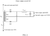
- FIG. 2 is a schematic diagram of a power output circuit 103 according to an embodiment of this application.
- the power output circuit 103 has two input ends: a first input end 1031 and a second input end 1032.
- the power output circuit 103 also has two output ends: a first output end 1033 and a second output end 1034.
- the first input end 1031 is connected to a bridge arm midpoint of a first bridge arm 101
- the second input end 1032 is connected to a bridge arm midpoint of a second bridge arm 102
- the first output end 1033 and the second output end 1034 are to two ends of a load R.
- the bridge arm midpoint refers to a junction between two MOSFETs of a corresponding bridge arm.
- the power output circuit 103 includes a resonant inductor L R , a transformer T, two diodes D1 and D2, an output inductor L OUT , and an output capacitor C OUT .
- the first input end 1031 of the power output circuit 103 is at one end of the resonant inductor L R
- the other end of the resonant inductor L R is connected to one end of a primary coil N P of the transformer T
- the second input end 1032 of the power output circuit 103 is at the other end of the primary coil N P of the transformer T.
- the transformer T has two secondary coils: a secondary coil N1 and a secondary coil N2.
- One end of the secondary coil N1 is connected to an anode of the diode D1, and a cathode of the diode D1 is connected to one end of the output inductor L OUT .
- the other end of the secondary coil N1 is connected to one end of the secondary coil N2, and the other end of the secondary coil N2 is connected to an anode of the diode D2.
- a cathode of the diode D2 is also connected to the one end of the output inductor L OUT , the other end of the output inductor L OUT is connected to one end of the load R, and the other end of the load R is connected to the other end of the secondary coil N1.
- the output capacitor C OUT is connected to the load R in parallel.
- That the output capacitor C OUT is connected to the load R in parallel means that one end of the output capacitor C OUT is connected to the first output end of the power output circuit, and that the other end of the output capacitor C OUT is connected to the second output end of the power output circuit.
- the first output end 1033 of the power output circuit 103 is at the other end of the output inductor L OUT
- the second output end 1034 of the power output circuit 103 is at the other end of the secondary coil N1 and the one end of the secondary coil N2.
- the second output end 1034 of the power output circuit 103 is grounded.
- the power output circuit shown in FIG. 1 or FIG. 2 may not include the resonant inductor L R . In this case, the two input ends of the power output circuit are at two ends of the primary coil of the transformer T. Other connection relationships are shown in FIG. 1 or FIG. 2 . Details are not repeated herein.
- the PSFB converter 100 may further include a filter capacitor C IN .
- the filter capacitor C IN is connected in parallel to the positive and negative power input ports of the PSFB converter, and is configured to perform filtering for the input power supply.
- the control circuit 104 when the PSFB converter is connected to the load R, as shown in FIG. 1 , the control circuit 104 further includes a voltage measurement port. The voltage measurement port is connected to the one end of the load R, and the control circuit 104 may determine voltages at two ends of the load R based on the voltage measurement port.
- a first drive signal DR1 and a second drive signal DR2 are a pair of complementary drive signals. That the first drive signal DR1 and the second drive signal DR2 are complementary means that when the first drive signal DR1 is a high-level signal, the second drive signal DR2 is a low-level signal, and that when the second drive signal DR2 is a high-level signal, the first drive signal DR1 is a low-level signal.
- a third drive signal DR3 and a fourth drive signal DR4 are a pair of complementary drive signals.
- the input power supply is short-circuited.
- a dead time is set between the first drive signal DR1 and the second drive signal DR2, and the dead time is a time in which the first drive signal DR1 and the second drive signal DR2 each are of a low-level. Accordingly, a dead time is also set between the third drive signal DR3 and the fourth drive signal DR4.
- the dead time is very short, for example, 0.5 ms or 1 ms.
- FIG. 3 is a schematic diagram of a drive signal according to an embodiment of this application. As shown in FIG. 3 , all four drive signals are periodic square wave signals. A first drive signal DR1 and a second drive signal DR2 are complementary to each other, and a third drive signal DR3 and a fourth drive signal DR4 are complementary to each other. A dead time is extremely short. Therefore, in FIG. 3 , a dead time between the first drive signal DR1 and the second drive signal DR2 and a dead time between the third drive signal DR3 and the fourth drive signal Drive4 are not marked.
- a phase difference between the first drive signal DR1 and the third drive signal DR3 is a positive value
- a phase difference between the second drive signal DR2 and the fourth drive signal DR4 is also a positive value. That a phase difference between the first drive signal DR1 and the third drive signal DR3 is a positive value means that it takes some time to align a rising edge of the first drive signal DR1 with a rising edge of the third drive signal DR3.
- the phase difference between the first drive signal DR1 and the third drive signal DR3 is the same as the phase difference between the second drive signal DR2 and the fourth drive signal DR4.
- a working process of a PSFB converter may be divided into the following stages.
- the first drive signal DR1 and the third drive signal DR3 each are a high-level signal, a first MOSFET M1 and a third MOSFET M3 each are in a conducting state, and current passing through a primary coil N P becomes larger.
- a speed at which the current becomes larger slows down because of self-coupling of the primary coil N P .
- the current passing through the primary coil N P becomes largest.
- the diode D1 is turned on, the diode D2 is turned off, and the secondary coil N1, the diode D1, an output inductor L OUT , and an output capacitor C OUT form a loop to supply energy to a load R.
- the first MOSFET M1 is turned off, and a second MOSFET M2 is turned on.
- the second MOSFET M2 and the third MOSFET M3 each are in a conducting state, and a resonant inductor L R , the primary coil N P , the second MOSFET M2, and the third MOSFET M3 form a circuit.
- Energy stored in the resonant inductor L R and the primary coil N P is discharged, and the current passing through the primary coil N P becomes smaller.
- the diode D1 is still turned on, the diode D2 is still turned off, and the secondary coil N1, the diode D1, the output inductor L OUT , and the output capacitor C OUT form a loop to supply energy to the load R.
- the third MOSFET M3 is turned off, and a fourth MOSFET M4 is turned on.
- the second MOSFET M2 and the fourth MOSFET M4 each are in a conducting state, and power is supplied to the second MOSFET M2 and the fourth MOSFET M4 by using an input power supply.
- the current passing through the primary coil N P is increased negatively.
- the current passing from the secondary coil N1 to the anode of the diode D1 is backward current, and the current passing from the secondary coil N2 to the anode of the diode D2 is forward current. Therefore, in the time period from t4 to t6, the diode D1 is turned off, the diode D2 is turned on, and the secondary coil N2, the diode D2, the output inductor L OUT , and the output capacitor C OUT form a loop to supply energy to the load R.
- the second MOSFET M2 is turned off, and the first MOSFET M1 is turned on.
- the first MOSFET M1 and the fourth MOSFET M4 each are in a conducting state.
- the resonant inductor L R , the transformer T, the first MOSFET M1, and the fourth MOSFET M4 form a circuit.
- Energy stored in the resonant inductor L R and the transformer is discharged, and the current passing through the primary coil N P becomes smaller.
- a next cycle begins. In this time period, the secondary coil N2, the diode D2, the output inductor LOUT, and the output capacitor C OUT form a loop to supply energy to the load R.
- a first bridge arm is a leading bridge arm
- a second bridge arm is a lagging bridge arm.
- the current at the moment t3 is greater than the current at the moment t4. Therefore, a turn-off loss of the first MOSFET M1 is greater than a turn-off loss of the third MOSFET M3, and similarly, a turn-off loss of the second MOSFET M2 is also greater than a turn-off loss of the fourth MOSFET M4. If the PSFB converter keeps operating under the drive signals shown in FIG. 3 , in other words, if a controller keeps controlling the first clock and the second clock to operate in the first state, a turn-off loss of the first bridge arm is greater than a turn-off loss of the second bridge arm in a quite long time period, resulting in low reliability of the PSFB converter.
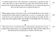
- FIG. 4 is a flowchart of a method for controlling a PSFB converter according to an embodiment of this application. The method is applied to the PSFB converter. As shown in FIG. 4 , the method includes the following steps.
- Step 401 A control circuit controls a first clock and a second clock to operate in a first state, and controls a timer to start timing, where when the first clock and the second clock operate in the first state, a first bridge arm is a leading bridge arm, and a second bridge arm is a lagging bridge arm.
- control circuit controls a first clock and a second clock to operate in a first state has been described in detail in the foregoing descriptions of the structure of the PSFB converter. Details are not repeated herein.
- the control circuit when the control circuit controls the first clock and the second clock to operate in the first state, the control circuit also needs to control the timer to start timing, so as to switch between the leading bridge arm and the lagging bridge arm after the first clock and the second clock operate in the first state for a time period, and improve reliability of the PSFB converter.
- Step 402 When timing duration of the timer reaches a first threshold, the control circuit controls the first clock and the second clock to switch to a second state, where when the first clock and the second clock operate in the second state, the first bridge arm is the lagging bridge arm, and the second bridge arm is the leading bridge arm.
- That the control circuit controls the first clock and the second clock to switch to a second state means that the control circuit re-outputs a first drive signal and a second drive signal based on the first clock and re-outputs a third drive signal and a fourth drive signal based on the second clock.
- a phase difference between the first drive signal and the third drive signal is a negative value
- a phase difference between the second drive signal and the fourth drive signal is also a negative value.
- the first bridge arm is the lagging bridge arm
- the second bridge arm is the leading bridge arm.
- step 402 may be specifically: setting the phase difference between the first drive signal and the third drive signal to an opposite number of a before-switching phase difference, where the before-switching phase difference is a phase difference between the first drive signal and the third drive signal when the first clock and the second clock operate in the first state.
- FIG. 5 is a schematic diagram of another drive signal according to an embodiment of this application.
- a phase difference between a first drive signal and a third drive signal is a negative value
- a phase difference between a second drive signal and a fourth drive signal is also a negative value.
- That a phase difference between a first drive signal and a third drive signal is a negative value means that it takes some time to align a rising edge of the third drive signal with a rising edge of the first drive signal.
- That a phase difference between a second drive signal and a fourth drive signal is a negative value means that it also takes some time to align a rising edge of the fourth drive signal with a rising edge of the second drive signal.
- the first drive signal and the third drive signal each are a high-level signal
- the first MOSFET M1 and the third MOSFET M3 each are in a conducting state
- current passing through a primary coil N P becomes larger.
- a speed at which the current becomes larger slows down because of self-coupling of the primary coil N P .
- the third MOSFET M3 is turned off, the fourth MOSFET M4 is turned on, the first MOSFET M1 and the fourth MOSFET M4 each are in a conducting state, a resonant inductor L R , a transformer T, the first MOSFET M1, and the fourth MOSFET M4 form a loop, energy stored in the resonant inductor L R and the transformer T is discharged, and the current passing through the primary coil N P becomes smaller.
- the first MOSFET M1 is turned off, the second MOSFET M2 is turned on, the second MOSFET M2 and the fourth MOSFET M4 each are in a conducting state, and power is supplied to the second MOSFET M2 and the fourth MOSFET M4 by using an input power supply V IN .
- the current passing through the primary coil N P is increased negatively.
- the speed at which the current becomes larger slows down because of self-coupling of the primary coil N P .
- the fourth MOSFET M4 is turned off, the third MOSFET M3 is turned on, the second MOSFET M2 and the third MOSFET M3 each are in a conducting state, the resonant inductor L R , the transformer T, the second MOSFET M2, and the third MOSFET M3 form a loop, the energy stored in the resonant inductor L R and the transformer T is discharged, and the current passing through the primary coil N P becomes smaller.
- a next cycle begins. As shown in FIG.
- the third MOSFET M3 is already turned on, and before the second MOSFET M2 and the fourth MOSFET M4 each are in the conducting state, the fourth MOSFET M4 is also already turned on. Therefore, based on the drive signals shown in FIG. 5 , the first bridge arm is the lagging bridge arm, and the second bridge arm becomes the leading bridge arm.
- the phase difference between the first drive signal and the third drive signal may be gradually changed until the phase difference between the first drive signal and the third drive signal is the opposite number of the before-switching phase difference, and wherein the control circuit is further configured to gradually change the drive frequency in a process of gradually changing the phase difference between the first drive signal and the third drive signal, so that a product of the phase difference and the drive frequency falls within a target range.
- the phase difference between the first drive signal and the third drive signal may be gradually decreased.
- the phase difference between the first drive signal and the third drive signal is 0, the phase difference between the first drive signal and the third drive signal is continuously decreased, until an absolute value of the phase difference between the first drive signal and the third drive signal is equal to the before-switching phase difference.
- An implementation of gradually decreasing the phase difference between the first drive signal and the third drive signal may be: determining whether a current phase difference between the first drive signal and the third drive signal is 0 at each rising edge of the first drive signal. If the current phase difference between the first drive signal and the third drive signal is not 0, a change amount is subtracted from the current phase difference between the first drive signal and the third drive signal, and a phase difference obtained through subtracting the change amount is used as the current phase difference between the first drive signal and the third drive signal. In other words, before the phase difference between the first drive signal and the third drive signal becomes 0, duration from a current moment to a moment at which the rising edge of the first drive signal is aligned with the rising edge of the third drive signal is subtracted at each rising edge of the first drive signal.
- the change amount may be preset or may be obtained through calculation. Change amounts for all changes may be the same or may be different. For example, when the change amounts for all the changes are the same, the change amount may be referred to as a step. Assuming that the before-switching phase difference is 30 and that the step is 1, after 30 rising edges of the first drive signal, the phase difference between the first drive signal and the third drive signal may be decreased to 0. For another example, when the change amounts for all the changes are different, a relatively large change amount may be set at an early stage of gradually changing the phase difference between the first drive signal and the third drive signal, and when the phase difference between the first drive signal and the third drive signal approximates to 0, the change amount is reduced.
- an implementation of continuously decreasing the phase difference between the first drive signal and the third drive signal is: determining, at each rising edge of the third drive signal, whether an absolute value of the current phase difference between the first drive signal and the third drive signal is the before-switching phase difference.
- the absolute value of the current phase difference between the first drive signal and the third drive signal is not the before-switching phase difference, a change amount is subtracted from the current phase difference between the first drive signal and the third drive signal, a phase difference obtained through subtracting the change amount is used as the current phase difference between the first drive signal and the third drive signal.
- duration from a current moment to a moment at which the rising edge of the third drive single is aligned with the rising edge of the first drive signal is added at each rising edge of the third drive signal.
- the change amount is set in a same manner as described above. Details are not repeated herein. For example, if the before-switching phase difference is 30 and the change amount is 1, after the phase difference between the first drive signal and the third drive signal becomes 0, the phase difference between the first drive signal and the third drive signal may become the opposite number of the before-switching phase difference after 30 rising edges of the third drive signal.
- a drive frequency is gradually changed in a process of gradually changing the phase difference between the first drive signal and the third drive signal, so that a product of the phase difference and the drive frequency falls within a target range.
- the drive frequency is gradually increased in a process of gradually decreasing the phase difference between the first drive signal and the third drive signal, so that a product of a decreased phase difference and an increased drive frequency falls within the target range.
- the drive frequency is gradually decreased in a process of continuously decreasing the phase difference between the first drive signal and the third drive signal, so that a product of an absolute value of a decreased phase difference and a decreased drive frequency falls within the target range.
- the absolute value of the phase difference between the first drive signal and the third drive signal is first decreased and then increased.
- the drive frequency is increased.
- the drive frequency is decreased.
- the first bridge arm can act as the leading bridge arm in one time period and act as the lagging bridge arm in another time period
- the second bridge arm can act as the lagging bridge arm in one time period and act as the leading bridge arm in another time period, so that a turn-off loss of the first bridge arm and a turn-off loss of the second bridge arm become almost the same, thereby improving reliability of the PSFB converter. Therefore, in a possible implementation, before the PSFB converter is used, a lifespan of the PSFB converter may be estimated, and the first threshold and a second threshold of the timer are set based on the lifespan of the PSFB converter. For example, the first threshold and the second threshold each may be a half of the estimated lifespan.
- the first bridge arm is the leading bridge arm and the second bridge arm is the lagging bridge arm for a half of usage time
- the first bridge arm is the lagging bridge arm and the second bridge arm is the leading bridge arm for another half of the usage time, so that the turn-off loss of the first bridge arm and the turn-off loss of the second bridge arm become almost the same.
- a specification of a MOSFET of the leading bridge arm is the same as that of a MOSFET of the lagging bridge arm, and a lifespan of the leading bridge arm is X and a lifespan of the lagging bridge arm is Y under a same usage condition, X is less than Y. If a controller keeps controlling the first clock and the second clock to operate in the first state, a lifespan of the first bridge arm is X, and a lifespan of the second bridge arm is Y. In this case, the lifespan of the PSFB converter is X.
- duration in which the first bridge arm acts as the leading bridge arm is almost the same as duration in which the second bridge arm acts as the leading bridge arm
- duration in which the first bridge arm acts as the lagging bridge arm is also almost the same as duration in which the second bridge arm acts as the lagging bridge arm.
- the lifespan of the first bridge arm is almost the same as the lifespan of the second bridge arm, both being 2XY/(X+Y).
- the lifespan of the PSFB converter is 2XY/(X+Y).
- X is less than Y, and therefore X is less than 2XY/(X+Y).
- X is 800 hours and Y is 1200 hours. If the controller keeps controlling the first clock and the second clock to operate in the first state, the lifespan of the PSFB converter is 800 hours. However, according to the control method provided in this embodiment of this application, the lifespan of the PSFB converter is 960 hours, thereby improving reliability of the PSFB converter.
- control circuit may further control the first clock and the second clock cycle to alternately operate in the first state and the second state, so as to improve reliability of the PSFB converter.
- control circuit further needs to continue to implement control by performing the following step 403.
- Step 403 The control circuit controls the timer to restart timing, and when new timing duration of the timer reaches a second threshold, the control circuit controls the first clock and the second clock to switch to the first state.
- the first threshold and the second threshold may be the same or may be different.
- the control circuit controls the first clock and the second clock to switch a working status each time the timing duration of the timer reaches the first threshold or the second threshold. This implements that the leading bridge arm and the lagging bridge arm are switched each time the timing duration reaches the first threshold or the second threshold.
- the first threshold or the second threshold may be randomly set, for example, both the first threshold and the second threshold are 100 hours. Each time the timing duration reaches 100 hours, the control circuit controls the first clock and the second clock to switch from the first state to the second state, or controls the first clock and the second clock to switch from the second state to the first state.
- a timing cycle of the timer may be: the first threshold, the second threshold, the second threshold, and the first threshold.
- the controller controls the first clock and the second clock to switch to the second state
- duration in which the controller control the first clock and the second clock to operate in the second state reaches the second threshold
- the controller controls the first clock and the second clock to switch to the second state
- duration in which the controller control the first clock and the second clock to operate in the second state reaches the first threshold
- the controller controls the first clock and the second clock to switch to the first state
- the first threshold is 100 hours
- the second threshold is 50 hours.
- the first clock and the second clock switch to the second state and operate in the second state for 50 hours, then switch to the first state and operate in the first state for 50 hours, and then switch to the second state and operate in the second state for 100 hours, so that the turn-off loss of the first bridge arm and the turn-off loss of the second bridge arm become almost the same.
- reliability of the PSFB converter is related to turn-off losses of the two bridge arms.
- a greater difference between the two turn-off losses corresponding to the two bridge arms indicates lower reliability of the PSFB converter.
- a turn-off loss of the leading bridge arm is greater than a turn-off loss of the lagging bridge arm. Therefore, in this application, after the control circuit of the PSFB converter controls the first clock and the second clock to operate in the first state for a time period, the control circuit controls the first clock and the second clock to switch to the second state.
- the first bridge arm When the first clock and the second clock operate in the first state, the first bridge arm is the leading bridge arm, and the second bridge arm is the lagging bridge arm, and when the first clock and the second clock operate in the second state, the first bridge arm is the lagging bridge arm, and the second bridge arm is the leading bridge arm. Therefore, according to the control method provided in this application, the first bridge arm can act as the leading bridge arm in one time period and act as the lagging bridge arm in another time period, and similarly, the second bridge arm can act as the lagging bridge arm in one time period and act as the leading bridge arm in another time period, so that the turn-off loss of the first bridge arm and the turn-off loss of the second bridge arm become almost the same, thereby improving reliability of the PSFB converter.
Landscapes
- Engineering & Computer Science (AREA)
- Power Engineering (AREA)
- Dc-Dc Converters (AREA)
Description
- This application relates to the field of power supply technologies, and in particular, to a phase-shifted full bridge (PSFB) converter control method and a PSFB converter.
- A PSFB converter is capable of converting direct current into direct current of different voltages (for example, direct current of a lower voltage). Reliability of the PSFB converter needs to be improved.
US2014/0177281 A1 discloses a full bridge converter in a power converting system and including a PSFB power converting system with a controller unit that is configured to balance the temperature of the legs of the converter.EP 1679783 A2 discloses a single stage switch mode power converter that receives a supply line voltage and a supply line current from a power supply line, and provides one or more regulated output voltages for a load, such as an amplifier.CN 103595274 A discloses a method for controlling a double-direction power flow high-frequency isolated active clamping rectifier.US 2014/092634 A1 discloses a mixed control method for a resonant converter, a resonant converter system and a mixed controller.CN 107070241 A discloses a method for controlling a PSFB converter. - This application provides a method for controlling a PSFB converter and a PSFB converter, to improve reliability of the PSFB converter. The technical solutions are as follows.
- According to a first aspect, a method for controlling a PSFB converter is provided, where the method includes:
controlling, by a control circuit, a first clock and a second clock to operate in a first state, and controlling a timer to start timing, where the PSFB converter includes a first bridge arm and a second bridge arm, the first bridge arm includes a first metal oxide semiconductor field effect transistor (MOSFET) and a second MOSFET, the second bridge arm includes a third MOSFET and a fourth MOSFET, a first drive signal output by the control circuit based on the first clock is input to a gate of the first MOSFET, a second drive signal output by the control circuit based on the first clock is input to a gate of the second MOSFET, a third drive signal output by the control circuit based on the second clock is input to a gate of the third MOSFET, a fourth drive signal output by the control circuit based on the second clock is input to a gate of the fourth MOSFET, the first drive signal, the second drive signal, the third drive signal, and the fourth drive signal are all periodic signals, frequencies of the first drive signal, the second drive signal, the third drive signal, and the fourth drive signal are the same and are drive frequencies, the first drive signal and the second drive signal are complementary to each other, the third drive signal and the fourth drive signal are complementary to each other, and when the first clock and the second clock operate in the first state, the first bridge arm is a leading bridge arm, and the second bridge arm is a lagging bridge arm; and controlling, by the control circuit when timing duration of the timer reaches a first threshold, the first clock and the second clock to switch to a second state, where when the first clock and the second clock operate in the second state, the first bridge arm is the lagging bridge arm, and the second bridge arm is the leading bridge arm, wherein the first bridge arm and the second bridge arm form a quadrilateral, the first MOSFET is at a first corner of the quadrilateral, the second MOSFET is at a second corner of the quadrilateral, the third MOSFET is at a third corner of the quadrilateral, the fourth MOSFET is at a fourth corner of the quadrilateral, the first corner and the third corner are opposite to each other, and the second corner and the fourth corner are opposite to each other, wherein the controlling, by the control circuit, the first clock and the second clock to switch to a second state comprises: setting a phase difference between the first drive signal and the third drive signal to an opposite number of a before-switching phase difference, wherein the before-switching phase difference is a phase difference between the first drive signal and the third drive signal when the first clock and the second clock operate in the first state, characterized in that the setting a phase difference between the first drive signal and the third drive signal to an opposite number of a before-switching phase difference comprises: gradually changing the phase difference between the first drive signal and the third drive signal until the phase difference between the first drive signal and the third drive signal is the opposite number of the before-switching phase difference, and wherein the method further comprises: gradually changing the drive frequency in a process of gradually changing the phase difference between the first drive signal and the third drive signal, so that a product of the phase difference and the drive frequency falls within a target range. - If the two bridge arms of the PSFB converter do not have a same lifespan, a lifespan of the PSFB converter depends on a bridge arm with a shorter lifespan of the two bridge arms. As a result, the PSFB converter has relatively low reliability. A lifespan of a bridge arm is related to a loss of the bridge arm. In the PSFB converter, a conduction loss and a turn-on loss of each of the four MOSFETs approximate to 0, and therefore a loss of each MOSFET is basically a turn-off loss of the MOSFET. Accordingly, a loss of each bridge arm also approximates to a sum of turn-off losses of two MOSFETs of the bridge arm. Therefore, a relatively large difference between two turn-off losses of two bridge arms affects reliability of the PSFB converter. In a working process of the PSFB converter, a turn-off loss of the leading bridge arm is greater than a turn-off loss of the lagging bridge arm. Therefore, in this application, the control circuit switches roles of the leading bridge arm and the lagging bridge arm after a working time reaches a threshold. Therefore, according to the control method provided in this application, the first bridge arm can act as the leading bridge arm in one time period and act as the lagging bridge arm in another time period, and similarly, the second bridge arm can act as the lagging bridge arm in one time period and act as the leading bridge arm in another time period, so that a turn-off loss of the first bridge arm and a turn-off loss of the second bridge arm become almost the same, thereby improving reliability of the PSFB converter.
- The first bridge arm and the second bridge arm form a quadrilateral, the first MOSFET is at a first corner of the quadrilateral, the second MOSFET is at a second corner of the quadrilateral, the third MOSFET is at a third corner of the quadrilateral, the fourth MOSFET is at a fourth corner of the quadrilateral, the first corner and the third corner are opposite to each other, and the second corner and the fourth corner are opposite to each other.
- Optionally, the controlling, by the control circuit, the first clock and the second clock to switch to a second state includes: setting a phase difference between the first drive signal and the third drive signal to an opposite number of a before-switching phase difference, where the before-switching phase difference is a phase difference between the first drive signal and the third drive signal when the first clock and the second clock operate in the first state.
- In this application, the control circuit may control, by changing the phase difference between the first drive signal and the third drive signal, the first clock and the second clock to switch to the second state. The phase difference between the first drive signal and the third drive signal is the before-switching phase difference when the first clock and the second clock operate in the first state. If the phase difference between the first drive signal and the third drive signal is set to the opposite number of the before-switching phase difference, the first clock and the second clock can be switched to the second state.
- Optionally, the setting a phase difference between the first drive signal and the third drive signal to an opposite number of a before-switching phase difference includes: gradually changing the phase difference between the first drive signal and the third drive signal until the phase difference between the first drive signal and the third drive signal is the opposite number of the before-switching phase difference.
- In this application, to avoid an abnormality of the PSFB converter caused by an abrupt change in the phase difference between the first drive signal and the third drive signal, the phase difference between the first drive signal and the third drive signal may be gradually changed when the phase difference between the first drive signal and the third drive signal is set to the opposite number of the before-switching phase difference.
- Optionally, the method further includes: gradually changing the drive frequency in a process of gradually changing the phase difference between the first drive signal and the third drive signal, so that a product of the phase difference and the drive frequency falls within a target range.
- When a voltage of an input power supply connected to the PSFB converter is fixed, voltages applied to two ends of a load by the PSFB converter are related to a duty cycle. The duty cycle is a product of the drive frequency and the phase difference between the first drive signal and the third drive signal. Therefore, in the process of changing the phase difference between the first drive signal and the third drive signal, the drive frequency is correspondingly adjusted to avoid a sharp change in the voltages at the two ends of the load. Optionally, the method further includes: controlling, by the control circuit when the control circuit controls the first clock and the second clock to switch to the second state, the timer to restart timing; and controlling, by the control circuit when new timing duration of the timer reaches a second threshold, the first clock and the second clock to switch to the first state.
- In this application, the first clock and the second clock cycle can be controlled to alternately operate in the first state and the second state, so as to improve reliability of the PSFB converter.
- According to a second aspect, a PSFB converter is provided, where the PSFB converter includes a first bridge arm, a second bridge arm, a power output circuit, and a control circuit.
- The first bridge arm and the second bridge arm are connected in parallel, the first bridge arm includes a first MOSFET and a second MOSFET, the second bridge arm includes a third MOSFET and a fourth MOSFET, a first input end of the power output circuit is connected to a bridge arm midpoint of the first bridge arm, and a second input end of the power output circuit is connected to a bridge arm midpoint of the second bridge arm.
- The control circuit includes a first clock, a second clock, and a timer, a first drive signal output by the control circuit based on the first clock is input to a gate of the first MOSFET, a second drive signal output by the control circuit based on the first clock is input to a gate of the second MOSFET, a third drive signal output by the control circuit based on the second clock is input to a gate of the third MOSFET, a fourth drive signal output by the control circuit based on the second clock is input to a gate of the fourth MOSFET, the first drive signal, the second drive signal, the third drive signal, and the fourth drive signal are all periodic signals, frequencies of the first drive signal, the second drive signal, the third drive signal, and the fourth drive signal are the same and are drive frequencies, the first drive signal and the second drive signal are complementary to each other, and the third drive signal and the fourth drive signal are complementary to each other.
- The control circuit provides a function of implementing the method for controlling a PSFB converter in the first aspect.
-
-
FIG. 1 is a schematic structural diagram of a PSFB converter according to an embodiment of this application; -
FIG. 2 is a schematic diagram of a power output circuit according to an embodiment of this application; -
FIG. 3 is a schematic diagram of a drive signal according to an embodiment of this application; -
FIG. 4 is a flowchart of a method for controlling a PSFB converter according to an embodiment of this application; and -
FIG. 5 is a schematic diagram of another drive signal according to an embodiment of this application. - To make the objectives, technical solutions, and advantages of this application clearer, the following further describes the implementations of this application in detail with reference to the accompanying drawings.
-
FIG. 1 is a schematic structural diagram of a PSFB converter according to an embodiment of this application. As shown inFIG. 1 , aPSFB converter 100 includes afirst bridge arm 101, asecond bridge arm 102, apower output circuit 103, and acontrol circuit 104. - As shown in
FIG. 1 , thePSFB converter 100 has positive and negative power input ports: a positive power input port V+ and a negative power input port V-. An input power supply may be connected to the PSFB converter by using the positive and negative power input ports, to transfer energy to a load by using the PSFB converter. Thefirst bridge arm 101 and thesecond bridge arm 102 are connected in parallel to the positive and negative power input ports of thePSFB converter 100. Thefirst bridge arm 101 includes a first MOSFET M1 and a second MOSFET M2, and thesecond bridge arm 102 includes a third MOSFET M3 and a fourth MOSFET M4. - That the
first bridge arm 101 is connected in parallel to the positive and negative power input ports of thePSFB converter 100 means that a drain of the first MOSFET M1 is connected to the positive power input port V+, and that a source of the first MOSFET M1 is connected to a drain of the second MOSFET M2. That thesecond bridge arm 102 is connected in parallel to the positive and negative power input ports of thePSFB converter 100 means that a source of the second MOSFET M2 is connected to the negative power input port V-. A drain of the fourth MOSFET M4 is connected to the positive power input port V+, and a source of the fourth MOSFET M4 is connected to a drain of the third MOSFET M3. A source of the third MOSFET M3 is connected to the negative power input port V-. The following can be learned from the connection relationships: the first bridge arm and the second bridge arm form a quadrilateral, the first MOSFET is at a first corner of the quadrilateral, the second MOSFET is at a second corner of the quadrilateral, the third MOSFET is at a third corner of the quadrilateral, the fourth MOSFET is at a fourth corner of the quadrilateral, the first corner and the third corner are opposite to each other, and the second corner and the fourth corner are opposite to each other. Sources and drains of one or more of the MOSFETs may be exchanged. - The
control circuit 104 includes a first clock T1, a second clock T2, and a timer T3. Thecontrol circuit 104 outputs a first drive signal DR1 and a second drive signal DR2 based on the first clock T1, and outputs a third drive signal DR3 and a fourth drive signal DR4 based on the second clock T2. The first drive signal DR1 is input to a gate of the first MOSFET M1, the second drive signal DR2 is input to a gate of the second MOSFET M2, the third drive signal DR3 is input to a gate of the third MOSFET M3, and the fourth drive signal Drive4 is input to a gate of the fourth MOSFET M2. In other words, the first drive signal output by the control circuit based on the first clock is input to the gate of the first MOSFET, the second drive signal output by the control circuit based on the first clock is input to the gate of the second MOSFET, the third drive signal output by the control circuit based on the second clock is input to the gate of the third MOSFET, and the fourth drive signal output by the control circuit based on the second clock is input to the gate of the fourth MOSFET. - The timer T3 is configured to perform timing. The
control circuit 104 controls the first clock T1 and the second clock T2 by using the timer T3, to implement the method for controlling a PSFB converter provided in the embodiments of this application. - Signals that the
control circuit 104 controls to generate based on the first clock and the second clock are digital signals. In this case, thecontrol circuit 104 may further include two drive circuits: a first drive circuit and a second drive circuit. The first drive circuit is connected to the first clock, and is configured to convert a digital signal generated by the first clock into the first drive signal and the second drive signal. The second drive circuit is connected to the second clock, and is configured to convert a digital signal generated by the second clock into the third drive signal and the fourth drive signal. - In addition, the
control circuit 104 further includes a control chip. The control chip may be an MCU, a field-programmable gate array (FPGA), a digital signal processor (DSP), or the like. The first drive circuit and the second drive circuit may be integrated into the control chip or may be disposed outside the control chip. This is not specifically limited in this embodiment of this application. - In addition, in this embodiment of this application, the
control circuit 104 has a plurality of power-on manners. For example, thecontrol circuit 104 may also include an additional power supply, and the additional power supply is configured to supply power to the control circuit. For another example, thecontrol circuit 104 is connected to the input power supply by using another converter, and the input power supply supplies power to thecontrol circuit 104 by using the another converter. The another converter is a voltage converter different from the PSFB converter, and is configured to convert a voltage of the input power supply to a voltage required by thecontrol circuit 104. For another example, when a voltage required by the load is almost the same as the voltage required by thecontrol circuit 104, thecontrol circuit 104 may also be directly connected to an output end of the PSFB converter, so that power is supplied to thecontrol circuit 104 by using the output end of the PSFB converter. - In addition, the first drive circuit and the second drive circuit also need to be powered on. For a specific power-on manner, refer to the power-on manners of the
control circuit 104. Details are not repeated herein. -
FIG. 2 is a schematic diagram of apower output circuit 103 according to an embodiment of this application. As shown inFIG. 2 , thepower output circuit 103 has two input ends: afirst input end 1031 and asecond input end 1032. Thepower output circuit 103 also has two output ends: afirst output end 1033 and asecond output end 1034. As shown inFIG. 1 , thefirst input end 1031 is connected to a bridge arm midpoint of afirst bridge arm 101, thesecond input end 1032 is connected to a bridge arm midpoint of asecond bridge arm 102, and thefirst output end 1033 and thesecond output end 1034 are to two ends of a load R. The bridge arm midpoint refers to a junction between two MOSFETs of a corresponding bridge arm. - In one possible implementation, as shown in
FIG. 1 orFIG. 2 , thepower output circuit 103 includes a resonant inductor LR, a transformer T, two diodes D1 and D2, an output inductor LOUT, and an output capacitor COUT. Thefirst input end 1031 of thepower output circuit 103 is at one end of the resonant inductor LR, the other end of the resonant inductor LR is connected to one end of a primary coil NP of the transformer T, and thesecond input end 1032 of thepower output circuit 103 is at the other end of the primary coil NP of the transformer T. The transformer T has two secondary coils: a secondary coil N1 and a secondary coil N2. One end of the secondary coil N1 is connected to an anode of the diode D1, and a cathode of the diode D1 is connected to one end of the output inductor LOUT. The other end of the secondary coil N1 is connected to one end of the secondary coil N2, and the other end of the secondary coil N2 is connected to an anode of the diode D2. A cathode of the diode D2 is also connected to the one end of the output inductor LOUT, the other end of the output inductor LOUT is connected to one end of the load R, and the other end of the load R is connected to the other end of the secondary coil N1. The output capacitor COUT is connected to the load R in parallel. That the output capacitor COUT is connected to the load R in parallel means that one end of the output capacitor COUT is connected to the first output end of the power output circuit, and that the other end of the output capacitor COUT is connected to the second output end of the power output circuit. Thefirst output end 1033 of thepower output circuit 103 is at the other end of the output inductor LOUT, and thesecond output end 1034 of thepower output circuit 103 is at the other end of the secondary coil N1 and the one end of the secondary coil N2. In addition, as shown inFIG. 1 , thesecond output end 1034 of thepower output circuit 103 is grounded. In another possible implementation, the power output circuit shown inFIG. 1 orFIG. 2 may not include the resonant inductor LR. In this case, the two input ends of the power output circuit are at two ends of the primary coil of the transformer T. Other connection relationships are shown inFIG. 1 orFIG. 2 . Details are not repeated herein. - Optionally, as shown in
FIG. 1 , thePSFB converter 100 may further include a filter capacitor CIN. The filter capacitor CIN is connected in parallel to the positive and negative power input ports of the PSFB converter, and is configured to perform filtering for the input power supply. Optionally, when the PSFB converter is connected to the load R, as shown inFIG. 1 , thecontrol circuit 104 further includes a voltage measurement port. The voltage measurement port is connected to the one end of the load R, and thecontrol circuit 104 may determine voltages at two ends of the load R based on the voltage measurement port. - For ease of description below, a working principle of the PSFB converter is first described herein.
- In this embodiment of this application, all four drive signals are periodic signals, and frequencies of the four drive signals are the same. For ease of description, the frequencies of the four drive signals are referred to as drive frequencies. A first drive signal DR1 and a second drive signal DR2 are a pair of complementary drive signals. That the first drive signal DR1 and the second drive signal DR2 are complementary means that when the first drive signal DR1 is a high-level signal, the second drive signal DR2 is a low-level signal, and that when the second drive signal DR2 is a high-level signal, the first drive signal DR1 is a low-level signal. Similarly, a third drive signal DR3 and a fourth drive signal DR4 are a pair of complementary drive signals.
- As shown in
FIG. 1 , when the first drive signal DR1 and the second drive signal DR2 each are a high-level signal, or when the third drive signal DR3 and the fourth drive signal DR4 each are a high-level signal, the input power supply is short-circuited. To avoid a short circuit, a dead time is set between the first drive signal DR1 and the second drive signal DR2, and the dead time is a time in which the first drive signal DR1 and the second drive signal DR2 each are of a low-level. Accordingly, a dead time is also set between the third drive signal DR3 and the fourth drive signal DR4. Usually, the dead time is very short, for example, 0.5 ms or 1 ms.FIG. 3 is a schematic diagram of a drive signal according to an embodiment of this application. As shown inFIG. 3 , all four drive signals are periodic square wave signals. A first drive signal DR1 and a second drive signal DR2 are complementary to each other, and a third drive signal DR3 and a fourth drive signal DR4 are complementary to each other. A dead time is extremely short. Therefore, inFIG. 3 , a dead time between the first drive signal DR1 and the second drive signal DR2 and a dead time between the third drive signal DR3 and the fourth drive signal Drive4 are not marked. - As shown in
FIG. 3 , a phase difference between the first drive signal DR1 and the third drive signal DR3 is a positive value, and a phase difference between the second drive signal DR2 and the fourth drive signal DR4 is also a positive value. That a phase difference between the first drive signal DR1 and the third drive signal DR3 is a positive value means that it takes some time to align a rising edge of the first drive signal DR1 with a rising edge of the third drive signal DR3. Because the first drive signal DR1 and the second drive signal DR2 are complementary to each other and the third drive signal DR3 and the fourth drive signal DR4 are complementary to each other, the phase difference between the first drive signal DR1 and the third drive signal DR3 is the same as the phase difference between the second drive signal DR2 and the fourth drive signal DR4. - Based on the drive signals shown in
FIG. 3 and the structure of the PSFB converter shown inFIG. 1 , as shown inFIG. 3 , a working process of a PSFB converter may be divided into the following stages. - At t1, the first drive signal DR1 and the third drive signal DR3 each are a high-level signal, a first MOSFET M1 and a third MOSFET M3 each are in a conducting state, and current passing through a primary coil NP becomes larger. At t2, a speed at which the current becomes larger slows down because of self-coupling of the primary coil NP. At t3, the current passing through the primary coil NP becomes largest.
- In this time period, the current passing through the primary coil NP keeps getting larger, and therefore current is generated in a secondary coil N1 and a secondary coil N2. There are dotted terminals between the primary coil NP of a transformer T and the two secondary coils (the dotted terminals between the primary coil NP and the two secondary coils are marked as black dots in
FIG. 1 ), and the dotted terminals are ports of a same current direction. It can be learned that in the time period from t1 to t3, current passing from the secondary coil N1 to an anode of a diode D1 is forward current, and current passing from the secondary coil N2 to an anode of a diode D2 is backward current. Therefore, in the time period from t1 to t3, the diode D1 is turned on, the diode D2 is turned off, and the secondary coil N1, the diode D1, an output inductor LOUT, and an output capacitor COUT form a loop to supply energy to a load R. - At t3, the first MOSFET M1 is turned off, and a second MOSFET M2 is turned on. At this time, the second MOSFET M2 and the third MOSFET M3 each are in a conducting state, and a resonant inductor LR, the primary coil NP, the second MOSFET M2, and the third MOSFET M3 form a circuit. Energy stored in the resonant inductor LR and the primary coil NP is discharged, and the current passing through the primary coil NP becomes smaller.
- In this time period, the diode D1 is still turned on, the diode D2 is still turned off, and the secondary coil N1, the diode D1, the output inductor LOUT, and the output capacitor COUT form a loop to supply energy to the load R.
- At t4, the third MOSFET M3 is turned off, and a fourth MOSFET M4 is turned on. At this time, the second MOSFET M2 and the fourth MOSFET M4 each are in a conducting state, and power is supplied to the second MOSFET M2 and the fourth MOSFET M4 by using an input power supply. The current passing through the primary coil NP is increased negatively.
- At t5, a speed at which the current becomes larger slows down because of self-coupling of the primary coil NP. At t6, the current passing through the primary coil NP is negatively increased to a largest value.
- In this time period, the current passing from the secondary coil N1 to the anode of the diode D1 is backward current, and the current passing from the secondary coil N2 to the anode of the diode D2 is forward current. Therefore, in the time period from t4 to t6, the diode D1 is turned off, the diode D2 is turned on, and the secondary coil N2, the diode D2, the output inductor LOUT, and the output capacitor COUT form a loop to supply energy to the load R.
- At t6, the second MOSFET M2 is turned off, and the first MOSFET M1 is turned on. At this time, the first MOSFET M1 and the fourth MOSFET M4 each are in a conducting state. At this time, the resonant inductor LR, the transformer T, the first MOSFET M1, and the fourth MOSFET M4 form a circuit. Energy stored in the resonant inductor LR and the transformer is discharged, and the current passing through the primary coil NP becomes smaller. At t7, a next cycle begins. In this time period, the secondary coil N2, the diode D2, the output inductor LOUT, and the output capacitor COUT form a loop to supply energy to the load R.
- As shown in
FIG. 3 , before the first MOSFET M1 and the third MOSFET M3 each are in the conducting state, the first MOSFET M1 is already turned on, and before the second MOSFET M2 and the fourth MOSFET M4 each are in the conducting state, the second MOSFET M2 is also already turned on. Therefore, under the control of the four drive signals shown inFIG. 3 , a first bridge arm is a leading bridge arm, and a second bridge arm is a lagging bridge arm. In this embodiment of this application, if four drive signals output by a first clock T1 and a second clock T2 are the drive signals shown inFIG. 3 , it is considered that the first clock and the second clock operate in a first state. - As shown in
FIG. 3 , the current at the moment t3 is greater than the current at the moment t4. Therefore, a turn-off loss of the first MOSFET M1 is greater than a turn-off loss of the third MOSFET M3, and similarly, a turn-off loss of the second MOSFET M2 is also greater than a turn-off loss of the fourth MOSFET M4. If the PSFB converter keeps operating under the drive signals shown inFIG. 3 , in other words, if a controller keeps controlling the first clock and the second clock to operate in the first state, a turn-off loss of the first bridge arm is greater than a turn-off loss of the second bridge arm in a quite long time period, resulting in low reliability of the PSFB converter. Therefore, an embodiment of this application provides a method for controlling a PSFB converter, to improve reliability of the PSFB converter.FIG. 4 is a flowchart of a method for controlling a PSFB converter according to an embodiment of this application. The method is applied to the PSFB converter. As shown inFIG. 4 , the method includes the following steps. - Step 401: A control circuit controls a first clock and a second clock to operate in a first state, and controls a timer to start timing, where when the first clock and the second clock operate in the first state, a first bridge arm is a leading bridge arm, and a second bridge arm is a lagging bridge arm.
- That the control circuit controls a first clock and a second clock to operate in a first state has been described in detail in the foregoing descriptions of the structure of the PSFB converter. Details are not repeated herein.
- In this embodiment of this application, to prevent the first bridge arm from always acting as the leading bridge arm and prevent the second bridge arm from always acting as the lagging bridge arm, when the control circuit controls the first clock and the second clock to operate in the first state, the control circuit also needs to control the timer to start timing, so as to switch between the leading bridge arm and the lagging bridge arm after the first clock and the second clock operate in the first state for a time period, and improve reliability of the PSFB converter.
- Step 402: When timing duration of the timer reaches a first threshold, the control circuit controls the first clock and the second clock to switch to a second state, where when the first clock and the second clock operate in the second state, the first bridge arm is the lagging bridge arm, and the second bridge arm is the leading bridge arm.
- That the control circuit controls the first clock and the second clock to switch to a second state means that the control circuit re-outputs a first drive signal and a second drive signal based on the first clock and re-outputs a third drive signal and a fourth drive signal based on the second clock. In this case, a phase difference between the first drive signal and the third drive signal is a negative value, and a phase difference between the second drive signal and the fourth drive signal is also a negative value. In this case, when the four drive signals are input to gates of four MOSFETs respectively in the manner shown in
FIG. 1 , the first bridge arm is the lagging bridge arm, and the second bridge arm is the leading bridge arm. - In this embodiment of this application, the phase difference between the first drive signal and the third drive signal is the same as the phase difference between the second drive signal and the fourth drive signal. Therefore, adjusting the phase difference between the first drive signal and the third drive signal is adjusting the phase difference between the second drive signal and the fourth drive signal. Therefore, in a possible implementation,
step 402 may be specifically: setting the phase difference between the first drive signal and the third drive signal to an opposite number of a before-switching phase difference, where the before-switching phase difference is a phase difference between the first drive signal and the third drive signal when the first clock and the second clock operate in the first state. -
FIG. 5 is a schematic diagram of another drive signal according to an embodiment of this application. As shown inFIG. 5 , a phase difference between a first drive signal and a third drive signal is a negative value, and a phase difference between a second drive signal and a fourth drive signal is also a negative value. That a phase difference between a first drive signal and a third drive signal is a negative value means that it takes some time to align a rising edge of the third drive signal with a rising edge of the first drive signal. That a phase difference between a second drive signal and a fourth drive signal is a negative value means that it also takes some time to align a rising edge of the fourth drive signal with a rising edge of the second drive signal. - In the drive signals shown in
FIG. 5 , at t1, the first drive signal and the third drive signal each are a high-level signal, the first MOSFET M1 and the third MOSFET M3 each are in a conducting state, and current passing through a primary coil NP becomes larger. At t2, a speed at which the current becomes larger slows down because of self-coupling of the primary coil NP. At t3, the third MOSFET M3 is turned off, the fourth MOSFET M4 is turned on, the first MOSFET M1 and the fourth MOSFET M4 each are in a conducting state, a resonant inductor LR, a transformer T, the first MOSFET M1, and the fourth MOSFET M4 form a loop, energy stored in the resonant inductor LR and the transformer T is discharged, and the current passing through the primary coil NP becomes smaller. At t4, the first MOSFET M1 is turned off, the second MOSFET M2 is turned on, the second MOSFET M2 and the fourth MOSFET M4 each are in a conducting state, and power is supplied to the second MOSFET M2 and the fourth MOSFET M4 by using an input power supply VIN. The current passing through the primary coil NP is increased negatively. At t5, the speed at which the current becomes larger slows down because of self-coupling of the primary coil NP. At t6, the fourth MOSFET M4 is turned off, the third MOSFET M3 is turned on, the second MOSFET M2 and the third MOSFET M3 each are in a conducting state, the resonant inductor LR, the transformer T, the second MOSFET M2, and the third MOSFET M3 form a loop, the energy stored in the resonant inductor LR and the transformer T is discharged, and the current passing through the primary coil NP becomes smaller. At t7, a next cycle begins. As shown inFIG. 5 , before the first MOSFET M1 and the third MOSFET M3 each are in the conducting state, the third MOSFET M3 is already turned on, and before the second MOSFET M2 and the fourth MOSFET M4 each are in the conducting state, the fourth MOSFET M4 is also already turned on. Therefore, based on the drive signals shown inFIG. 5 , the first bridge arm is the lagging bridge arm, and the second bridge arm becomes the leading bridge arm. - Further, to avoid an abnormality of the PSFB converter caused by an abrupt change in the phase difference between the first drive signal and the third drive signal, when the phase difference between the first drive signal and the third drive signal is set to an opposite number of a before-switching phase difference, the phase difference between the first drive signal and the third drive signal may be gradually changed until the phase difference between the first drive signal and the third drive signal is the opposite number of the before-switching phase difference, and wherein the control circuit is further configured to gradually change the drive frequency in a process of gradually changing the phase difference between the first drive signal and the third drive signal, so that a product of the phase difference and the drive frequency falls within a target range.
- In a possible implementation, the phase difference between the first drive signal and the third drive signal may be gradually decreased. When the phase difference between the first drive signal and the third drive signal is 0, the phase difference between the first drive signal and the third drive signal is continuously decreased, until an absolute value of the phase difference between the first drive signal and the third drive signal is equal to the before-switching phase difference.
- An implementation of gradually decreasing the phase difference between the first drive signal and the third drive signal may be: determining whether a current phase difference between the first drive signal and the third drive signal is 0 at each rising edge of the first drive signal. If the current phase difference between the first drive signal and the third drive signal is not 0, a change amount is subtracted from the current phase difference between the first drive signal and the third drive signal, and a phase difference obtained through subtracting the change amount is used as the current phase difference between the first drive signal and the third drive signal. In other words, before the phase difference between the first drive signal and the third drive signal becomes 0, duration from a current moment to a moment at which the rising edge of the first drive signal is aligned with the rising edge of the third drive signal is subtracted at each rising edge of the first drive signal.
- The change amount may be preset or may be obtained through calculation. Change amounts for all changes may be the same or may be different. For example, when the change amounts for all the changes are the same, the change amount may be referred to as a step. Assuming that the before-switching phase difference is 30 and that the step is 1, after 30 rising edges of the first drive signal, the phase difference between the first drive signal and the third drive signal may be decreased to 0. For another example, when the change amounts for all the changes are different, a relatively large change amount may be set at an early stage of gradually changing the phase difference between the first drive signal and the third drive signal, and when the phase difference between the first drive signal and the third drive signal approximates to 0, the change amount is reduced.
- In addition, after the phase difference between the first drive signal and the third drive signal becomes 0, if the phase difference between the first drive signal and the third drive signal continues to be decreased, the phase difference between the first drive signal and the third drive signal becomes a negative value. In other words, it takes some time to align the rising edge of the third drive signal with the rising edge of the first drive signal. Therefore, an implementation of continuously decreasing the phase difference between the first drive signal and the third drive signal is: determining, at each rising edge of the third drive signal, whether an absolute value of the current phase difference between the first drive signal and the third drive signal is the before-switching phase difference. If the absolute value of the current phase difference between the first drive signal and the third drive signal is not the before-switching phase difference, a change amount is subtracted from the current phase difference between the first drive signal and the third drive signal, a phase difference obtained through subtracting the change amount is used as the current phase difference between the first drive signal and the third drive signal. In other words, before the absolute value of the phase difference between the first drive signal and the third drive signal is increased to the before-switching phase difference, duration from a current moment to a moment at which the rising edge of the third drive single is aligned with the rising edge of the first drive signal is added at each rising edge of the third drive signal.
- The change amount is set in a same manner as described above. Details are not repeated herein. For example, if the before-switching phase difference is 30 and the change amount is 1, after the phase difference between the first drive signal and the third drive signal becomes 0, the phase difference between the first drive signal and the third drive signal may become the opposite number of the before-switching phase difference after 30 rising edges of the third drive signal.
- Further, to make voltages at two ends of a load remain stable, a drive frequency is gradually changed in a process of gradually changing the phase difference between the first drive signal and the third drive signal, so that a product of the phase difference and the drive frequency falls within a target range.
- For example, in a possible implementation of gradually changing the phase difference between the first drive signal and the third drive signal, the drive frequency is gradually increased in a process of gradually decreasing the phase difference between the first drive signal and the third drive signal, so that a product of a decreased phase difference and an increased drive frequency falls within the target range. The drive frequency is gradually decreased in a process of continuously decreasing the phase difference between the first drive signal and the third drive signal, so that a product of an absolute value of a decreased phase difference and a decreased drive frequency falls within the target range.
- It should be noted that there is a dead time between the first drive signal and the second drive signal and that there is also a dead time between the third drive signal and the fourth drive signal. Therefore, in the process of changing the phase difference between the first drive signal and the third drive signal, the phase difference between the first drive signal and the third drive signal is unlikely to be 0. In other words, in the process of changing the phase difference between the first drive signal and the third drive signal, when the phase difference between the first drive signal and the third drive signal is decreased until approaching 0, the phase difference between the first drive signal and the third drive signal becomes a negative value if the phase difference between the first drive signal and the third drive signal continues to be decreased.
- In the process of changing the phase difference between the first drive signal and the third drive signal, the absolute value of the phase difference between the first drive signal and the third drive signal is first decreased and then increased. In a process of decreasing the absolute value of the phase difference between the first drive signal and the third drive signal, the drive frequency is increased. In a process of increasing the absolute value of the phase difference between the first drive signal and the third drive signal, the drive frequency is decreased. When the PSFB converter is connected to the load, because a voltage required by the load is usually within a given range, a voltage output by the input power supply by using the PSFB converter needs to be maintained within the given range. Assuming that the voltage of the input power supply is Vin, and that the voltage outputted by the input power supply by using the PSFB converter is Vo, a duty cycle of the PSFB converter may be expressed as D=nV0/Vin, where n is a turn ratio of a primary turn to a secondary turn of the transformer. The duty cycle of the PSFB converter may alternatively be expressed as D=phase×f, where phase is the phase difference between the first drive signal and the third drive signal, and f is the drive frequency. Therefore, if the voltages applied to the two ends of the load need to remain within a range, the duty cycle also needs to remain within a value range, and this value range is the target range.
- According to step 401 and step 402, the first bridge arm can act as the leading bridge arm in one time period and act as the lagging bridge arm in another time period, and similarly, the second bridge arm can act as the lagging bridge arm in one time period and act as the leading bridge arm in another time period, so that a turn-off loss of the first bridge arm and a turn-off loss of the second bridge arm become almost the same, thereby improving reliability of the PSFB converter. Therefore, in a possible implementation, before the PSFB converter is used, a lifespan of the PSFB converter may be estimated, and the first threshold and a second threshold of the timer are set based on the lifespan of the PSFB converter. For example, the first threshold and the second threshold each may be a half of the estimated lifespan. In this way, in an entire process of using the PSFB converter, the first bridge arm is the leading bridge arm and the second bridge arm is the lagging bridge arm for a half of usage time, and the first bridge arm is the lagging bridge arm and the second bridge arm is the leading bridge arm for another half of the usage time, so that the turn-off loss of the first bridge arm and the turn-off loss of the second bridge arm become almost the same.
- If a specification of a MOSFET of the leading bridge arm is the same as that of a MOSFET of the lagging bridge arm, and a lifespan of the leading bridge arm is X and a lifespan of the lagging bridge arm is Y under a same usage condition, X is less than Y. If a controller keeps controlling the first clock and the second clock to operate in the first state, a lifespan of the first bridge arm is X, and a lifespan of the second bridge arm is Y. In this case, the lifespan of the PSFB converter is X. However, if the controller controls the first clock and the second clock according to the method provided in this embodiment of this application, duration in which the first bridge arm acts as the leading bridge arm is almost the same as duration in which the second bridge arm acts as the leading bridge arm, and duration in which the first bridge arm acts as the lagging bridge arm is also almost the same as duration in which the second bridge arm acts as the lagging bridge arm. In this case, the lifespan of the first bridge arm is almost the same as the lifespan of the second bridge arm, both being 2XY/(X+Y). In this case, the lifespan of the PSFB converter is 2XY/(X+Y). X is less than Y, and therefore X is less than 2XY/(X+Y). It can be learned that the control method provided in this embodiment of this application can improve the lifespan of the PSFB converter, thereby improving reliability of the PSFB converter.
- For example, X is 800 hours and Y is 1200 hours. If the controller keeps controlling the first clock and the second clock to operate in the first state, the lifespan of the PSFB converter is 800 hours. However, according to the control method provided in this embodiment of this application, the lifespan of the PSFB converter is 960 hours, thereby improving reliability of the PSFB converter.
- Optionally, in this embodiment of this application, the control circuit may further control the first clock and the second clock cycle to alternately operate in the first state and the second state, so as to improve reliability of the PSFB converter. In this case, after
step 402, the control circuit further needs to continue to implement control by performing the followingstep 403. - Step 403: The control circuit controls the timer to restart timing, and when new timing duration of the timer reaches a second threshold, the control circuit controls the first clock and the second clock to switch to the first state.
- The first threshold and the second threshold may be the same or may be different. When the first threshold is the same as the second threshold, it indicates that when specified timing duration in the timer is the first threshold or the second threshold, the control circuit controls the first clock and the second clock to switch a working status each time the timing duration of the timer reaches the first threshold or the second threshold. This implements that the leading bridge arm and the lagging bridge arm are switched each time the timing duration reaches the first threshold or the second threshold.
- The first threshold or the second threshold may be randomly set, for example, both the first threshold and the second threshold are 100 hours. Each time the timing duration reaches 100 hours, the control circuit controls the first clock and the second clock to switch from the first state to the second state, or controls the first clock and the second clock to switch from the second state to the first state.
- When the first threshold is different from the second threshold, to make the turn-off loss of the first bridge arm and the turn-off loss of the second bridge arm become almost the same, a timing cycle of the timer may be: the first threshold, the second threshold, the second threshold, and the first threshold. In this case, when duration in which the controller controls the first clock and the second clock to operate in the first state reaches the first threshold, the controller controls the first clock and the second clock to switch to the second state, and when duration in which the controller control the first clock and the second clock to operate in the second state reaches the second threshold, the controller controls the first clock and the second clock to switch to the first state. When duration in which the controller controls the first clock and the second clock to operate in the first state reaches the second threshold, the controller controls the first clock and the second clock to switch to the second state, and when duration in which the controller control the first clock and the second clock to operate in the second state reaches the first threshold, the controller controls the first clock and the second clock to switch to the first state.
- For example, the first threshold is 100 hours, and the second threshold is 50 hours. In this case, after having operated in the first state for 100 hours, the first clock and the second clock switch to the second state and operate in the second state for 50 hours, then switch to the first state and operate in the first state for 50 hours, and then switch to the second state and operate in the second state for 100 hours, so that the turn-off loss of the first bridge arm and the turn-off loss of the second bridge arm become almost the same.
- In addition, for an implementation of controlling, by the control circuit, the first clock and the second clock to switch to the first state, refer to the implementation of controlling, by the control circuit, the first clock and the second clock to switch to the second state in
step 402. Details are not repeated herein. - In this embodiment of this application, reliability of the PSFB converter is related to turn-off losses of the two bridge arms. To be specific, a greater difference between the two turn-off losses corresponding to the two bridge arms indicates lower reliability of the PSFB converter. In a working process of the PSFB converter, a turn-off loss of the leading bridge arm is greater than a turn-off loss of the lagging bridge arm. Therefore, in this application, after the control circuit of the PSFB converter controls the first clock and the second clock to operate in the first state for a time period, the control circuit controls the first clock and the second clock to switch to the second state. When the first clock and the second clock operate in the first state, the first bridge arm is the leading bridge arm, and the second bridge arm is the lagging bridge arm, and when the first clock and the second clock operate in the second state, the first bridge arm is the lagging bridge arm, and the second bridge arm is the leading bridge arm. Therefore, according to the control method provided in this application, the first bridge arm can act as the leading bridge arm in one time period and act as the lagging bridge arm in another time period, and similarly, the second bridge arm can act as the lagging bridge arm in one time period and act as the leading bridge arm in another time period, so that the turn-off loss of the first bridge arm and the turn-off loss of the second bridge arm become almost the same, thereby improving reliability of the PSFB converter.
Claims (4)
- A method for controlling a phase-shifted full bridge, PSFB, converter (100), wherein
the method comprises:Controlling (401), by a control circuit (104), a first clock (T1) and a second clock (T2) to operate in a first state, and controlling a timer to start timing, whereinthe PSFB converter comprises a first bridge arm (101) and a second bridge arm (102), the first bridge arm comprises a first metal oxide semiconductor field effect transistor, MOSFET, and a second MOSFET, the second bridge arm comprises a third MOSFET and a fourth MOSFET, a first drive signal (DR1) output by the control circuit based on the first clock is input to a gate of the first MOSFET, a second drive signal (DR2) output by the control circuit based on the first clock is input to a gate of the second MOSFET, a third drive signal (DR3) output by the control circuit based on the second clock is input to a gate of the third MOSFET, a fourth drive signal (DR4) output by the control circuit based on the second clock is input to a gate of the fourth MOSFET, the first drive signal, the second drive signal, the third drive signal, and the fourth drive signal are all periodic signals, frequencies of the first drive signal, the second drive signal, the third drive signal, and the fourth drive signal are the same and are drive frequencies, the first drive signal and the second drive signal are complementary to each other, the third drive signal and the fourth drive signal are complementary to each other, and when the first clock and the second clock operate in the first state, the first bridge arm is a leading bridge arm, and the second bridge arm is a lagging bridge arm; andcontrolling (402), by the control circuit (104) when timing duration of the timer reaches a first threshold, the first clock and the second clock to switch to a second state, wherein when the first clock and the second clock operate in the second state, the first bridge arm is the lagging bridge arm, and the second bridge arm is the leading bridge arm,wherein the first bridge arm (101) and the second bridge arm (102) form a quadrilateral, the first MOSFET is at a first corner of the quadrilateral, the second MOSFET is at a second corner of the quadrilateral, the third MOSFET is at a third corner of the quadrilateral, the fourth MOSFET is at a fourth corner of the quadrilateral, the first corner and the third corner are opposite to each other, and the second corner and the fourth corner are opposite to each other,wherein the controlling, by the control circuit, the first clock (T1) and the second clock (T2) to switch to a second state comprises:setting a phase difference between the first drive signal (DR1) and the third drive signal (DR3) to an opposite number of a before-switching phase difference, wherein the before-switching phase difference is a phase difference between the first drive signal and the third drive signal when the first clock and the second clock operate in the first state,characterized in that the setting a phase difference between the first drive signal (DR1) and the third drive signal (DR3) to an opposite number of a before-switching phase difference comprises:
gradually changing the phase difference between the first drive signal and the third drive signal until the phase difference between the first drive signal and the third drive signal is the opposite number of the before-switching phase difference, and wherein the method further comprises:
gradually changing the drive frequency in a process of gradually changing the phase difference between the first drive signal (DR1) and the third drive signal (DR3), so that a product of the phase difference and the drive frequency falls within a target range. - The method according to claim 1, wherein the method further comprises:controlling, by the control circuit (104) when the control circuit controls the first clock (T1) and the second clock (T2) to switch to the second state, the timer to restart timing; andcontrolling, by the control circuit (104) when new timing duration of the timer reaches a second threshold, the first clock and the second clock to switch to the first state.
- A phase-shifted full bridge PSFB converter (100), wherein the, PSFB, converter comprises a first bridge arm, a second bridge arm, a power output circuit, and a control circuit, whereinthe first bridge arm (101) and the second bridge arm (102) are connected in parallel, the first bridge arm comprises a first metal oxide semiconductor field effect transistor, MOSFET, and a second MOSFET, the second bridge arm comprises a third MOSFET and a fourth MOSFET, a first input end of the power output circuit is connected to a bridge arm midpoint of the first bridge arm, and a second input end of the power output circuit is connected to a bridge arm midpoint of the second bridge arm;the control circuit comprises a first clock (T1), a second clock (T2), and a timer, a first drive signal (DR1) output by the control circuit based on the first clock is input to a gate of the first MOSFET, a second drive signal (DR2) output by the control circuit based on the first clock is input to a gate of the second MOSFET, a third drive signal (DR3) output by the control circuit based on the second clock is input to a gate of the third MOSFET, a fourth drive signal (DR4) output by the control circuit based on the second clock is input to a gate of the fourth MOSFET, the first drive signal, the second drive signal, the third drive signal, and the fourth drive signal are all periodic signals, frequencies of the first drive signal, the second drive signal, the third drive signal, and the fourth drive signal are the same and are drive frequencies, the first drive signal and the second drive signal are complementary to each other, and the third drive signal and the fourth drive signal are complementary to each other;the control circuit (104) is configured to control the first clock and the second clock to operate in a first state, and control the timer to start timing, and when the first clock and the second clock operate in the first state, the first bridge arm (1010 is a leading bridge arm, and the second bridge arm (102) is a lagging bridge arm; andthe control circuit (104) is further configured to: when timing duration of the timer reaches a first threshold, control the first clock and the second clock to switch to a second state, wherein when the first clock and the second clock operate in the second state, the first bridge arm is the lagging bridge arm, and the second bridge arm is the leading bridge arm,wherein the first bridge arm (101) and the second bridge arm (102) form a quadrilateral, the first MOSFET is at a first corner of the quadrilateral, the second MOSFET is at a second corner of the quadrilateral, the third MOSFET is at a third corner of the quadrilateral, the fourth MOSFET is at a fourth corner of the quadrilateral, the first corner and the third corner are opposite to each other, and the second corner and the fourth corner are opposite to each other,wherein the control circuit (104) is specifically configured to:set a phase difference between the first drive signal (DR1) and the third drive signal (DR3) to an opposite number of a before-switching phase difference, wherein the before-switching phase difference is a phase difference between the first drive signal and the third drive signal when the first clock and the second clock operate in the first state,characterized in that the control circuit is specifically configured to:
gradually change the phase difference between the first drive signal and the third drive signal until the phase difference between the first drive signal and the third drive signal is the opposite number of the before-switching phase difference, and wherein the control circuit (104) is further configured to gradually change the drive frequency in a process of gradually changing the phase difference between the first drive signal (DR1) and the third drive signal (DR3), so that a product of the phase difference and the drive frequency falls within a target range. - The PSFB converter according to any one of claims 2 and 3, wherein the control circuit (104) is further configured to:
when controlling the first clock and the second clock to switch to the second state, control the timer to restart timing, and when new timing duration of the timer reaches a second threshold, control the first clock (T1) and the second clock (T2) to switch to the first state.
Applications Claiming Priority (1)
| Application Number | Priority Date | Filing Date | Title |
|---|---|---|---|
| CN201810547340.4A CN110557022B (en) | 2018-05-31 | 2018-05-31 | Method for controlling PSFB converter and PSFB converter |
Publications (2)
| Publication Number | Publication Date |
|---|---|
| EP3576277A1 EP3576277A1 (en) | 2019-12-04 |
| EP3576277B1 true EP3576277B1 (en) | 2022-07-27 |
Family
ID=66685425
Family Applications (1)
| Application Number | Title | Priority Date | Filing Date |
|---|---|---|---|
| EP19177639.2A Active EP3576277B1 (en) | 2018-05-31 | 2019-05-31 | Method for controlling a psfb converter and psfb converter |
Country Status (3)
| Country | Link |
|---|---|
| US (1) | US10784786B2 (en) |
| EP (1) | EP3576277B1 (en) |
| CN (1) | CN110557022B (en) |
Families Citing this family (3)
| Publication number | Priority date | Publication date | Assignee | Title |
|---|---|---|---|---|
| CN111478572B (en) * | 2020-04-13 | 2021-02-19 | 北京理工大学 | Single-pole AC-DC converter modal smooth switching and power factor correction control method |
| EP4102703A1 (en) * | 2021-06-09 | 2022-12-14 | Delta Electronics (Thailand) Public Co., Ltd. | Alternating asymmetrical phase-shift modulation |
| CN114825961B (en) * | 2022-04-28 | 2026-03-27 | 华为数字能源技术有限公司 | Controllers, power supply modules, and electronic devices used to control phase-shifted full-bridge circuits. |
Citations (1)
| Publication number | Priority date | Publication date | Assignee | Title |
|---|---|---|---|---|
| CN107070241A (en) * | 2017-06-06 | 2017-08-18 | 西北工业大学 | The heat balance control method of the double active bridging parallel operation power devices of aviation |
Family Cites Families (8)
| Publication number | Priority date | Publication date | Assignee | Title |
|---|---|---|---|---|
| US7283379B2 (en) * | 2005-01-07 | 2007-10-16 | Harman International Industries, Incorporated | Current controlled switch mode power supply |
| US7652899B2 (en) * | 2007-05-30 | 2010-01-26 | Delphi Technologies, Inc. | Switching sequence control method for a PS-ZVT bridge converter |
| CN101386099A (en) * | 2008-10-28 | 2009-03-18 | 上海沪工电焊机制造有限公司 | Soft-switch invert welding power numerical control method of electric welding machine |
| CN103715906B (en) * | 2012-09-29 | 2017-05-24 | 台达电子工业股份有限公司 | Resonant converter hybrid control method, resonant converter system and hybrid controller |
| CN104113215B (en) * | 2012-11-27 | 2017-03-22 | 台达电子工业股份有限公司 | DC-DC converter and control method thereof |
| TW201427246A (en) * | 2012-12-26 | 2014-07-01 | Yen-Shin Lai | Phase-shift full-bridge converter and the controlling thereof |
| CN103595274B (en) * | 2013-11-27 | 2017-02-08 | 东南大学 | Method for controlling double-direction power flow high-frequency isolated active clamping rectifier |
| CN106849652B (en) * | 2017-02-17 | 2019-03-19 | 国电南瑞科技股份有限公司 | A 0°~360° digital phase shift control method and system |
-
2018
- 2018-05-31 CN CN201810547340.4A patent/CN110557022B/en not_active Expired - Fee Related
-
2019
- 2019-05-30 US US16/426,962 patent/US10784786B2/en not_active Expired - Fee Related
- 2019-05-31 EP EP19177639.2A patent/EP3576277B1/en active Active
Patent Citations (1)
| Publication number | Priority date | Publication date | Assignee | Title |
|---|---|---|---|---|
| CN107070241A (en) * | 2017-06-06 | 2017-08-18 | 西北工业大学 | The heat balance control method of the double active bridging parallel operation power devices of aviation |
Also Published As
| Publication number | Publication date |
|---|---|
| CN110557022A (en) | 2019-12-10 |
| US20190372468A1 (en) | 2019-12-05 |
| US10784786B2 (en) | 2020-09-22 |
| EP3576277A1 (en) | 2019-12-04 |
| CN110557022B (en) | 2021-05-14 |
Similar Documents
| Publication | Publication Date | Title |
|---|---|---|
| US8248046B2 (en) | DC-DC converter for pulse frequency modulation control and power supply system | |
| US6535400B2 (en) | Control circuit for synchronous rectifiers in DC/DC converters to reduce body diode conduction losses | |
| US8912773B2 (en) | Synchronous buck converter including multi-mode control for light load efficiency and related method | |
| US7456620B2 (en) | Determining dead times in switched-mode DC-DC converters | |
| CN205105103U (en) | Single -phase resonant transformation ware and heterogeneous resonant transformation ware | |
| US20150002115A1 (en) | Series-capacitor buck converter multiphase controller | |
| US20050110475A1 (en) | Adaptive delay control circuit for switched mode power supply | |
| US11070135B2 (en) | Converter with soft-start period of output voltage | |
| US8198881B2 (en) | Chopper type DC-DC converter | |
| CN101944848B (en) | Multi mode modulator and method with improved dynamic load regulation | |
| JP4955728B2 (en) | Method and apparatus for digital power processing operated by zero voltage switching | |
| US20200336070A1 (en) | Method for improving conversion efficiency of ccm mode of flyback resonant switch power supply | |
| EP3576277A1 (en) | Method for controlling a psfb converter and psfb converter | |
| CN110994988B (en) | BUCK-BOOST converter circuit and control method thereof | |
| US10491105B1 (en) | Power converter and dead-time control circuit therefor | |
| TWI899512B (en) | Dc/dc converter | |
| EP3783789A1 (en) | Control method for controlling resonant power converter, and resonant power converter | |
| CN105359278A (en) | Active diode having improved transistor turn-off control method | |
| US10587192B2 (en) | DC-DC voltage reducing converter with a test mode operation | |
| JPH06225522A (en) | Switching power supply circuit | |
| US20200382002A1 (en) | Power converter and method of operating the same | |
| EP3920400A1 (en) | Buck-boost circuit and control method therefor | |
| CN106059300B (en) | A kind of voltage changer based on pulse over-cycle phase width modulated mode | |
| TW201729525A (en) | Switching regulator | |
| CN114614675B (en) | Control circuit with power saving mode for power supply circuit |
Legal Events
| Date | Code | Title | Description |
|---|---|---|---|
| PUAI | Public reference made under article 153(3) epc to a published international application that has entered the european phase |
Free format text: ORIGINAL CODE: 0009012 |
|
| STAA | Information on the status of an ep patent application or granted ep patent |
Free format text: STATUS: THE APPLICATION HAS BEEN PUBLISHED |
|
| AK | Designated contracting states |
Kind code of ref document: A1 Designated state(s): AL AT BE BG CH CY CZ DE DK EE ES FI FR GB GR HR HU IE IS IT LI LT LU LV MC MK MT NL NO PL PT RO RS SE SI SK SM TR |
|
| AX | Request for extension of the european patent |
Extension state: BA ME |
|
| STAA | Information on the status of an ep patent application or granted ep patent |
Free format text: STATUS: REQUEST FOR EXAMINATION WAS MADE |
|
| 17P | Request for examination filed |
Effective date: 20200323 |
|
| RBV | Designated contracting states (corrected) |
Designated state(s): AL AT BE BG CH CY CZ DE DK EE ES FI FR GB GR HR HU IE IS IT LI LT LU LV MC MK MT NL NO PL PT RO RS SE SI SK SM TR |
|
| STAA | Information on the status of an ep patent application or granted ep patent |
Free format text: STATUS: EXAMINATION IS IN PROGRESS |
|
| 17Q | First examination report despatched |
Effective date: 20210222 |
|
| GRAP | Despatch of communication of intention to grant a patent |
Free format text: ORIGINAL CODE: EPIDOSNIGR1 |
|
| STAA | Information on the status of an ep patent application or granted ep patent |
Free format text: STATUS: GRANT OF PATENT IS INTENDED |
|
| INTG | Intention to grant announced |
Effective date: 20220318 |
|
| GRAS | Grant fee paid |
Free format text: ORIGINAL CODE: EPIDOSNIGR3 |
|
| GRAA | (expected) grant |
Free format text: ORIGINAL CODE: 0009210 |
|
| STAA | Information on the status of an ep patent application or granted ep patent |
Free format text: STATUS: THE PATENT HAS BEEN GRANTED |
|
| AK | Designated contracting states |
Kind code of ref document: B1 Designated state(s): AL AT BE BG CH CY CZ DE DK EE ES FI FR GB GR HR HU IE IS IT LI LT LU LV MC MK MT NL NO PL PT RO RS SE SI SK SM TR |
|
| REG | Reference to a national code |
Ref country code: CH Ref legal event code: EP |
|
| REG | Reference to a national code |
Ref country code: AT Ref legal event code: REF Ref document number: 1507748 Country of ref document: AT Kind code of ref document: T Effective date: 20220815 |
|
| REG | Reference to a national code |
Ref country code: DE Ref legal event code: R096 Ref document number: 602019017376 Country of ref document: DE |
|
| REG | Reference to a national code |
Ref country code: IE Ref legal event code: FG4D |
|
| REG | Reference to a national code |
Ref country code: LT Ref legal event code: MG9D |
|
| REG | Reference to a national code |
Ref country code: NL Ref legal event code: MP Effective date: 20220727 |
|
| PG25 | Lapsed in a contracting state [announced via postgrant information from national office to epo] |
Ref country code: SE Free format text: LAPSE BECAUSE OF FAILURE TO SUBMIT A TRANSLATION OF THE DESCRIPTION OR TO PAY THE FEE WITHIN THE PRESCRIBED TIME-LIMIT Effective date: 20220727 Ref country code: RS Free format text: LAPSE BECAUSE OF FAILURE TO SUBMIT A TRANSLATION OF THE DESCRIPTION OR TO PAY THE FEE WITHIN THE PRESCRIBED TIME-LIMIT Effective date: 20220727 Ref country code: PT Free format text: LAPSE BECAUSE OF FAILURE TO SUBMIT A TRANSLATION OF THE DESCRIPTION OR TO PAY THE FEE WITHIN THE PRESCRIBED TIME-LIMIT Effective date: 20221128 Ref country code: NO Free format text: LAPSE BECAUSE OF FAILURE TO SUBMIT A TRANSLATION OF THE DESCRIPTION OR TO PAY THE FEE WITHIN THE PRESCRIBED TIME-LIMIT Effective date: 20221027 Ref country code: NL Free format text: LAPSE BECAUSE OF FAILURE TO SUBMIT A TRANSLATION OF THE DESCRIPTION OR TO PAY THE FEE WITHIN THE PRESCRIBED TIME-LIMIT Effective date: 20220727 Ref country code: LV Free format text: LAPSE BECAUSE OF FAILURE TO SUBMIT A TRANSLATION OF THE DESCRIPTION OR TO PAY THE FEE WITHIN THE PRESCRIBED TIME-LIMIT Effective date: 20220727 Ref country code: LT Free format text: LAPSE BECAUSE OF FAILURE TO SUBMIT A TRANSLATION OF THE DESCRIPTION OR TO PAY THE FEE WITHIN THE PRESCRIBED TIME-LIMIT Effective date: 20220727 Ref country code: FI Free format text: LAPSE BECAUSE OF FAILURE TO SUBMIT A TRANSLATION OF THE DESCRIPTION OR TO PAY THE FEE WITHIN THE PRESCRIBED TIME-LIMIT Effective date: 20220727 Ref country code: ES Free format text: LAPSE BECAUSE OF FAILURE TO SUBMIT A TRANSLATION OF THE DESCRIPTION OR TO PAY THE FEE WITHIN THE PRESCRIBED TIME-LIMIT Effective date: 20220727 |
|
| REG | Reference to a national code |
Ref country code: AT Ref legal event code: MK05 Ref document number: 1507748 Country of ref document: AT Kind code of ref document: T Effective date: 20220727 |
|
| PG25 | Lapsed in a contracting state [announced via postgrant information from national office to epo] |
Ref country code: PL Free format text: LAPSE BECAUSE OF FAILURE TO SUBMIT A TRANSLATION OF THE DESCRIPTION OR TO PAY THE FEE WITHIN THE PRESCRIBED TIME-LIMIT Effective date: 20220727 Ref country code: IS Free format text: LAPSE BECAUSE OF FAILURE TO SUBMIT A TRANSLATION OF THE DESCRIPTION OR TO PAY THE FEE WITHIN THE PRESCRIBED TIME-LIMIT Effective date: 20221127 Ref country code: HR Free format text: LAPSE BECAUSE OF FAILURE TO SUBMIT A TRANSLATION OF THE DESCRIPTION OR TO PAY THE FEE WITHIN THE PRESCRIBED TIME-LIMIT Effective date: 20220727 Ref country code: GR Free format text: LAPSE BECAUSE OF FAILURE TO SUBMIT A TRANSLATION OF THE DESCRIPTION OR TO PAY THE FEE WITHIN THE PRESCRIBED TIME-LIMIT Effective date: 20221028 |
|
| PG25 | Lapsed in a contracting state [announced via postgrant information from national office to epo] |
Ref country code: SM Free format text: LAPSE BECAUSE OF FAILURE TO SUBMIT A TRANSLATION OF THE DESCRIPTION OR TO PAY THE FEE WITHIN THE PRESCRIBED TIME-LIMIT Effective date: 20220727 Ref country code: RO Free format text: LAPSE BECAUSE OF FAILURE TO SUBMIT A TRANSLATION OF THE DESCRIPTION OR TO PAY THE FEE WITHIN THE PRESCRIBED TIME-LIMIT Effective date: 20220727 Ref country code: DK Free format text: LAPSE BECAUSE OF FAILURE TO SUBMIT A TRANSLATION OF THE DESCRIPTION OR TO PAY THE FEE WITHIN THE PRESCRIBED TIME-LIMIT Effective date: 20220727 Ref country code: CZ Free format text: LAPSE BECAUSE OF FAILURE TO SUBMIT A TRANSLATION OF THE DESCRIPTION OR TO PAY THE FEE WITHIN THE PRESCRIBED TIME-LIMIT Effective date: 20220727 Ref country code: AT Free format text: LAPSE BECAUSE OF FAILURE TO SUBMIT A TRANSLATION OF THE DESCRIPTION OR TO PAY THE FEE WITHIN THE PRESCRIBED TIME-LIMIT Effective date: 20220727 |
|
| REG | Reference to a national code |
Ref country code: DE Ref legal event code: R097 Ref document number: 602019017376 Country of ref document: DE |
|
| PG25 | Lapsed in a contracting state [announced via postgrant information from national office to epo] |
Ref country code: SK Free format text: LAPSE BECAUSE OF FAILURE TO SUBMIT A TRANSLATION OF THE DESCRIPTION OR TO PAY THE FEE WITHIN THE PRESCRIBED TIME-LIMIT Effective date: 20220727 Ref country code: EE Free format text: LAPSE BECAUSE OF FAILURE TO SUBMIT A TRANSLATION OF THE DESCRIPTION OR TO PAY THE FEE WITHIN THE PRESCRIBED TIME-LIMIT Effective date: 20220727 |
|
| PLBE | No opposition filed within time limit |
Free format text: ORIGINAL CODE: 0009261 |
|
| STAA | Information on the status of an ep patent application or granted ep patent |
Free format text: STATUS: NO OPPOSITION FILED WITHIN TIME LIMIT |
|
| PG25 | Lapsed in a contracting state [announced via postgrant information from national office to epo] |
Ref country code: AL Free format text: LAPSE BECAUSE OF FAILURE TO SUBMIT A TRANSLATION OF THE DESCRIPTION OR TO PAY THE FEE WITHIN THE PRESCRIBED TIME-LIMIT Effective date: 20220727 |
|
| 26N | No opposition filed |
Effective date: 20230502 |
|
| PGFP | Annual fee paid to national office [announced via postgrant information from national office to epo] |
Ref country code: DE Payment date: 20230404 Year of fee payment: 5 |
|
| PG25 | Lapsed in a contracting state [announced via postgrant information from national office to epo] |
Ref country code: SI Free format text: LAPSE BECAUSE OF FAILURE TO SUBMIT A TRANSLATION OF THE DESCRIPTION OR TO PAY THE FEE WITHIN THE PRESCRIBED TIME-LIMIT Effective date: 20220727 |
|
| REG | Reference to a national code |
Ref country code: CH Ref legal event code: PL |
|
| PG25 | Lapsed in a contracting state [announced via postgrant information from national office to epo] |
Ref country code: MC Free format text: LAPSE BECAUSE OF FAILURE TO SUBMIT A TRANSLATION OF THE DESCRIPTION OR TO PAY THE FEE WITHIN THE PRESCRIBED TIME-LIMIT Effective date: 20220727 |
|
| GBPC | Gb: european patent ceased through non-payment of renewal fee |
Effective date: 20230531 |
|
| REG | Reference to a national code |
Ref country code: BE Ref legal event code: MM Effective date: 20230531 |
|
| PG25 | Lapsed in a contracting state [announced via postgrant information from national office to epo] |
Ref country code: MC Free format text: LAPSE BECAUSE OF FAILURE TO SUBMIT A TRANSLATION OF THE DESCRIPTION OR TO PAY THE FEE WITHIN THE PRESCRIBED TIME-LIMIT Effective date: 20220727 Ref country code: LU Free format text: LAPSE BECAUSE OF NON-PAYMENT OF DUE FEES Effective date: 20230531 Ref country code: LI Free format text: LAPSE BECAUSE OF NON-PAYMENT OF DUE FEES Effective date: 20230531 Ref country code: CH Free format text: LAPSE BECAUSE OF NON-PAYMENT OF DUE FEES Effective date: 20230531 |
|
| REG | Reference to a national code |
Ref country code: IE Ref legal event code: MM4A |
|
| PG25 | Lapsed in a contracting state [announced via postgrant information from national office to epo] |
Ref country code: IE Free format text: LAPSE BECAUSE OF NON-PAYMENT OF DUE FEES Effective date: 20230531 |
|
| PG25 | Lapsed in a contracting state [announced via postgrant information from national office to epo] |
Ref country code: IE Free format text: LAPSE BECAUSE OF NON-PAYMENT OF DUE FEES Effective date: 20230531 Ref country code: GB Free format text: LAPSE BECAUSE OF NON-PAYMENT OF DUE FEES Effective date: 20230531 |
|
| PG25 | Lapsed in a contracting state [announced via postgrant information from national office to epo] |
Ref country code: IT Free format text: LAPSE BECAUSE OF FAILURE TO SUBMIT A TRANSLATION OF THE DESCRIPTION OR TO PAY THE FEE WITHIN THE PRESCRIBED TIME-LIMIT Effective date: 20220727 Ref country code: FR Free format text: LAPSE BECAUSE OF NON-PAYMENT OF DUE FEES Effective date: 20230531 Ref country code: BE Free format text: LAPSE BECAUSE OF NON-PAYMENT OF DUE FEES Effective date: 20230531 |
|
| PG25 | Lapsed in a contracting state [announced via postgrant information from national office to epo] |
Ref country code: BG Free format text: LAPSE BECAUSE OF FAILURE TO SUBMIT A TRANSLATION OF THE DESCRIPTION OR TO PAY THE FEE WITHIN THE PRESCRIBED TIME-LIMIT Effective date: 20220727 |
|
| PG25 | Lapsed in a contracting state [announced via postgrant information from national office to epo] |
Ref country code: BG Free format text: LAPSE BECAUSE OF FAILURE TO SUBMIT A TRANSLATION OF THE DESCRIPTION OR TO PAY THE FEE WITHIN THE PRESCRIBED TIME-LIMIT Effective date: 20220727 |
|
| REG | Reference to a national code |
Ref country code: DE Ref legal event code: R119 Ref document number: 602019017376 Country of ref document: DE |
|
| PG25 | Lapsed in a contracting state [announced via postgrant information from national office to epo] |
Ref country code: DE Free format text: LAPSE BECAUSE OF NON-PAYMENT OF DUE FEES Effective date: 20241203 |
|
| PG25 | Lapsed in a contracting state [announced via postgrant information from national office to epo] |
Ref country code: CY Free format text: LAPSE BECAUSE OF FAILURE TO SUBMIT A TRANSLATION OF THE DESCRIPTION OR TO PAY THE FEE WITHIN THE PRESCRIBED TIME-LIMIT; INVALID AB INITIO Effective date: 20190531 |
|
| PG25 | Lapsed in a contracting state [announced via postgrant information from national office to epo] |
Ref country code: HU Free format text: LAPSE BECAUSE OF FAILURE TO SUBMIT A TRANSLATION OF THE DESCRIPTION OR TO PAY THE FEE WITHIN THE PRESCRIBED TIME-LIMIT; INVALID AB INITIO Effective date: 20190531 |
|
| PG25 | Lapsed in a contracting state [announced via postgrant information from national office to epo] |
Ref country code: TR Free format text: LAPSE BECAUSE OF FAILURE TO SUBMIT A TRANSLATION OF THE DESCRIPTION OR TO PAY THE FEE WITHIN THE PRESCRIBED TIME-LIMIT Effective date: 20220727 |