EP3572969A1 - Landing electrical contact - Google Patents
Landing electrical contact Download PDFInfo
- Publication number
- EP3572969A1 EP3572969A1 EP19175265.8A EP19175265A EP3572969A1 EP 3572969 A1 EP3572969 A1 EP 3572969A1 EP 19175265 A EP19175265 A EP 19175265A EP 3572969 A1 EP3572969 A1 EP 3572969A1
- Authority
- EP
- European Patent Office
- Prior art keywords
- wiring assembly
- profile
- electrical
- rigid
- curved
- Prior art date
- Legal status (The legal status is an assumption and is not a legal conclusion. Google has not performed a legal analysis and makes no representation as to the accuracy of the status listed.)
- Granted
Links
Images







Classifications
-
- G—PHYSICS
- G06—COMPUTING OR CALCULATING; COUNTING
- G06K—GRAPHICAL DATA READING; PRESENTATION OF DATA; RECORD CARRIERS; HANDLING RECORD CARRIERS
- G06K7/00—Methods or arrangements for sensing record carriers, e.g. for reading patterns
- G06K7/10—Methods or arrangements for sensing record carriers, e.g. for reading patterns by electromagnetic radiation, e.g. optical sensing; by corpuscular radiation
- G06K7/10009—Methods or arrangements for sensing record carriers, e.g. for reading patterns by electromagnetic radiation, e.g. optical sensing; by corpuscular radiation sensing by radiation using wavelengths larger than 0.1 mm, e.g. radio-waves or microwaves
-
- G—PHYSICS
- G06—COMPUTING OR CALCULATING; COUNTING
- G06K—GRAPHICAL DATA READING; PRESENTATION OF DATA; RECORD CARRIERS; HANDLING RECORD CARRIERS
- G06K7/00—Methods or arrangements for sensing record carriers, e.g. for reading patterns
- G06K7/0013—Methods or arrangements for sensing record carriers, e.g. for reading patterns by galvanic contacts, e.g. card connectors for ISO-7816 compliant smart cards or memory cards, e.g. SD card readers
- G06K7/0021—Methods or arrangements for sensing record carriers, e.g. for reading patterns by galvanic contacts, e.g. card connectors for ISO-7816 compliant smart cards or memory cards, e.g. SD card readers for reading/sensing record carriers having surface contacts
- G06K7/0026—Methods or arrangements for sensing record carriers, e.g. for reading patterns by galvanic contacts, e.g. card connectors for ISO-7816 compliant smart cards or memory cards, e.g. SD card readers for reading/sensing record carriers having surface contacts the galvanic contacts of the connector adapted for landing on the contacts of the card upon card insertion
-
- H—ELECTRICITY
- H01—ELECTRIC ELEMENTS
- H01R—ELECTRICALLY-CONDUCTIVE CONNECTIONS; STRUCTURAL ASSOCIATIONS OF A PLURALITY OF MUTUALLY-INSULATED ELECTRICAL CONNECTING ELEMENTS; COUPLING DEVICES; CURRENT COLLECTORS
- H01R13/00—Details of coupling devices of the kinds covered by groups H01R12/70 or H01R24/00 - H01R33/00
- H01R13/02—Contact members
- H01R13/22—Contacts for co-operating by abutting
- H01R13/24—Contacts for co-operating by abutting resilient; resiliently-mounted
- H01R13/2407—Contacts for co-operating by abutting resilient; resiliently-mounted characterized by the resilient means
-
- G—PHYSICS
- G06—COMPUTING OR CALCULATING; COUNTING
- G06F—ELECTRIC DIGITAL DATA PROCESSING
- G06F21/00—Security arrangements for protecting computers, components thereof, programs or data against unauthorised activity
- G06F21/70—Protecting specific internal or peripheral components, in which the protection of a component leads to protection of the entire computer
- G06F21/82—Protecting input, output or interconnection devices
- G06F21/85—Protecting input, output or interconnection devices interconnection devices, e.g. bus-connected or in-line devices
-
- G—PHYSICS
- G06—COMPUTING OR CALCULATING; COUNTING
- G06K—GRAPHICAL DATA READING; PRESENTATION OF DATA; RECORD CARRIERS; HANDLING RECORD CARRIERS
- G06K7/00—Methods or arrangements for sensing record carriers, e.g. for reading patterns
- G06K7/0013—Methods or arrangements for sensing record carriers, e.g. for reading patterns by galvanic contacts, e.g. card connectors for ISO-7816 compliant smart cards or memory cards, e.g. SD card readers
- G06K7/0047—Methods or arrangements for sensing record carriers, e.g. for reading patterns by galvanic contacts, e.g. card connectors for ISO-7816 compliant smart cards or memory cards, e.g. SD card readers for reading/sensing record carriers having edge contacts
-
- G—PHYSICS
- G11—INFORMATION STORAGE
- G11C—STATIC STORES
- G11C16/00—Erasable programmable read-only memories
- G11C16/02—Erasable programmable read-only memories electrically programmable
- G11C16/06—Auxiliary circuits, e.g. for writing into memory
- G11C16/10—Programming or data input circuits
-
- H—ELECTRICITY
- H01—ELECTRIC ELEMENTS
- H01R—ELECTRICALLY-CONDUCTIVE CONNECTIONS; STRUCTURAL ASSOCIATIONS OF A PLURALITY OF MUTUALLY-INSULATED ELECTRICAL CONNECTING ELEMENTS; COUPLING DEVICES; CURRENT COLLECTORS
- H01R12/00—Structural associations of a plurality of mutually-insulated electrical connecting elements, specially adapted for printed circuits, e.g. printed circuit boards [PCB], flat or ribbon cables, or like generally planar structures, e.g. terminal strips, terminal blocks; Coupling devices specially adapted for printed circuits, flat or ribbon cables, or like generally planar structures; Terminals specially adapted for contact with, or insertion into, printed circuits, flat or ribbon cables, or like generally planar structures
- H01R12/70—Coupling devices
- H01R12/77—Coupling devices for flexible printed circuits, flat or ribbon cables or like structures
- H01R12/771—Details
-
- H—ELECTRICITY
- H05—ELECTRIC TECHNIQUES NOT OTHERWISE PROVIDED FOR
- H05K—PRINTED CIRCUITS; CASINGS OR CONSTRUCTIONAL DETAILS OF ELECTRIC APPARATUS; MANUFACTURE OF ASSEMBLAGES OF ELECTRICAL COMPONENTS
- H05K1/00—Printed circuits
- H05K1/02—Details
- H05K1/0277—Bendability or stretchability details
- H05K1/028—Bending or folding regions of flexible printed circuits
- H05K1/0281—Reinforcement details thereof
-
- H—ELECTRICITY
- H05—ELECTRIC TECHNIQUES NOT OTHERWISE PROVIDED FOR
- H05K—PRINTED CIRCUITS; CASINGS OR CONSTRUCTIONAL DETAILS OF ELECTRIC APPARATUS; MANUFACTURE OF ASSEMBLAGES OF ELECTRICAL COMPONENTS
- H05K1/00—Printed circuits
- H05K1/02—Details
- H05K1/03—Use of materials for the substrate
- H05K1/0393—Flexible materials
Definitions
- the present teachings relate to the field of memory devices and product marking, for example, products including a tag or label for authentication and/or inventory control and, more particularly, to readers and scanners for reading and/or writing data from/to a product marked with an electronic memory, tag, or label.
- Xerox Printed Memory is a highly secure printed label including rewritable memory.
- the labels may be used for authentication to determine whether a product is authentic or genuine to prevent counterfeiting.
- the printed memory may be attached as a label onto a subassembly of a customer-replaceable unit such as various consumable components, supplies, shipment packaging, consumer products, documents, etc.
- Data from the printed memory may be read, for example, after installation of the unit to which it is attached into a host device and compared to an expected result or value. If the value read from the printed memory matches the expected value, circuitry within the host device allows the host device to function. If the value read from the printed memory does not match the expected value, the circuitry disables functionality of the host device until an authentic or genuine unit is installed.
- Xerox Printed Memory may be used to track a product through a manufacturing process and/or a supply chain.
- the labels can be programmed to mark individual items with a unique electronic identifier that may be verified with a scanner.
- Other uses for Xerox Printed Memory are contemplated including, but not limited to, smart consumables where an object is associated with data that is later used by a base unit to improve or optimize performance, consumption records where bulk usage of a product supply is tracked, tracking of items or people outside of a manufacturing environment, etc.
- a Xerox Printed Memory includes a layer of ferroelectric or ferrite material (i.e., a ferroelectric layer) positioned between a plurality of wiring lines (e.g., word lines and bit lines). A region of the ferroelectric layer situated between each bit line and word line forms a memory cell.
- the memory may be written with one of two digital memory states by applying a suitable write voltage to the wiring lines.
- the memory state may be read by applying a suitable read voltage to the wiring lines through electrical contacts (e.g., landings or landing pads).
- the ferroelectric material may be formed by various manufacturing processes.
- the printed memory device will display particular electrical characteristics. For example, for a given read voltage, different compositions of the ferroelectric layer return different output values.
- the manufacture and composition of the memory itself is difficult to counterfeit and provides secure and reliable anti-counterfeiting measures and reliable product tracking.
- An electrical device reader can include a wiring assembly having a flexible substrate and a plurality of electrical contacts supported by the flexible substrate.
- the device reader can further include an electrical connector electrically coupled with the plurality of electrical contacts, wherein the wiring assembly is configured to flex from a first profile in which the plurality of electrical contacts are not electrically coupled with a plurality of contact pads of an electrical device into a second profile in which the plurality of electrical contacts are electrically coupled with the plurality of contact pads of the electrical device.
- the first profile can be a flat profile and the second profile can be a curved profile.
- the electrical device reader can further include a cradle positioned relative to the electrical connector and having a curved surface that defines a recess in the cradle, wherein the wiring assembly is configured to flex and conform to the curved surface of the cradle into a curved profile during a transfer of data from and/or to an electrical device through the wiring assembly.
- the cradle can define a first channel and a second channel and the electrical connector can include a first tab and a second tab, where the first tab is positioned within the first channel, the second tab is positioned within the second channel, and the first and second tabs are configured to slide within the first and second channels.
- the electrical connector can be configured to slide back and forth within the recess defined by the curved surface of the cradle.
- the flexible substrate can include a flexible underlayer, wherein the flexible underlayer includes one or more of a synthetic foam, a urethane foam, a urethane foam rubber, and felt.
- the electrical connector can include a first carriage and a second carriage
- the cradle can include a first slot and a second slot
- the first and second carriages can be positioned within the first and second slots, thereby constraining movement of the electrical connector relative to the cradle along a path.
- the flexible substrate can include a rigid first portion and at least a rigid second portion, and the rigid first portion and the rigid second portion can be configured to articulate between a first position having the first profile and a second position having the second profile.
- the electrical device can further include a positioner that elastically maintains the wiring assembly in the first position having the first profile.
- the plurality of electrical contacts can include a plurality of spring-loaded electrical contacts.
- the electrical device reader can further include a driver mechanism configured to reposition the wiring assembly from the first position to the second position.
- the electronic device reader described above can be part of an electronic device, wherein the electronic device further includes a replaceable component having a curved surface and an electrical device attached to the curved surface of the replaceable component and having a curved profile.
- the wiring assembly of the electronic device reader can be configured to flex from a first profile in which the plurality of electrical contacts are not electrically coupled with a plurality of contact pads of the electrical device into a second profile in which the plurality of electrical contacts are electrically coupled with the plurality of contact pads of the electrical device.
- a method for authenticating a replaceable component of a host device can include positioning a wiring assembly in a first position adjacent to a curved printed memory, wherein a plurality of electrical contacts of the wiring assembly do not electrically couple with a plurality of contact pads of the curved printed memory, and the wiring assembly has a first profile in the first position and repositioning the wiring assembly into a second position, wherein the plurality of electrical contacts of the wiring assembly are electrically coupled with the plurality of contact pads of the curved printed memory and the wiring assembly has a second profile in the second position.
- data can be read from the curved printed memory.
- the method can further include comparing the data read from the curved printed memory to expected data. Responsive to the data read from the curved printed memory matching the expected data, functionality of the host device can be enabled and, responsive to the data read from the curved printed memory not matching the expected data, functionality of the host device can be disabled.
- the repositioning of the wiring assembly into the second position can include flexing a flexible underlayer of the wiring assembly from a flat profile to a curved profile.
- the repositioning of the wiring assembly into the second position can include articulating a rigid first portion of the wiring assembly and at least a second rigid second portion of the wiring assembly between the first position and the second position, and can further include engaging the rigid first portion and the rigid second portion with a driver mechanism thereby repositioning the rigid first portion and the rigid second portion from the first position to the second position and repositioning the wiring assembly from the second position into the first position using a positioner that elastically maintains the rigid first portion and the rigid second portion in the first position.
- data refers to any type of information, signals, or results that are obtained from or sent to an electrical device such as a memory device, an integrated circuit, or another electrical device, or any information obtained from monitoring, interrogating, querying, or measuring, etc., an electrical device.
- data includes digital data, analog data, voltage values, current values, resistance values, vector values, scalar values, and/or flux values.
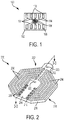
- FIG. 1 printed memory 100 includes a substrate 102, for example, a flexible dielectric substrate 102, such as a flexible polymer substrate, that may include an adhesive backing layer to aid in attachment of the printed memory 100 to a surface of a product, a plurality of wiring lines (e.g., word lines and bit lines) 104 and a ferroelectric layer 106 directly interposed or positioned between the word lines and the bit lines.
- a substrate 102 for example, a flexible dielectric substrate 102, such as a flexible polymer substrate, that may include an adhesive backing layer to aid in attachment of the printed memory 100 to a surface of a product, a plurality of wiring lines (e.g., word lines and bit lines) 104 and a ferroelectric layer 106 directly interposed or positioned between the word lines and the bit lines.
- a memory cell that stores the logic bit or logic state is provided by and within the ferroelectric layer 106 at the physical location that is interposed between the intersection of each word line and bit line. It will thus be appreciated that the word lines and bit lines do not physically intersect, but are physically separated by the ferroelectric layer 106.
- the printed memory 100 depicted in FIG. 1 includes 10 wiring lines 104 (five word lines and five bit lines), and thus the FIG. 1 device includes 25 memory cells and may thus store 25 bits of information. Each wiring line 104 terminates in a contact pad 108. It will be appreciated that a Xerox Printed Memory may include other structures that are not described or depicted for simplicity, while various depicted structures may be removed or modified.
- Each memory cell of the printed memory 100 may be read by applying a suitable read voltage to two of the wiring lines 104 (i.e., to one word line and one bit line) and measuring an electrical response.
- the plurality of contact pads 108 can be physically and electrically contacted with probe contacts of a reader. A voltage is applied across the contact pads 108 through probe contacts, and the resulting response is measured.
- Each memory cell may individually addressed during a read or write cycle, and two or more, or all, of the memory cells in the memory array may be read or written simultaneously or serially.
- the contact pads 108 of the printed memory 100 and other electrical devices can be formed using a carbon-impregnated composite, electrically conductive inks such as silver nanoparticle ink, or one or more other suitable materials.
- the probe contacts of the reader can be placed into physical contact with the contact pads 108 in a direction that is perpendicular to the plane of the contact pads 108, thereby minimizing wear or scratching from the physical contact.
- the printed memory 100 may be placed onto arcuate or curved surfaces.
- An implementation of the present teachings provides a reader that may be used with printed memory 100, such as Xerox Printed Memory 100, or another memory device or electrical device.
- the reader can be a standalone device such as a handheld reader, or can be integrated as a subsystem of another electronic host device such as a printer.
- the printed memory 100 can be placed onto a curved surface, such as an exterior surface of a toner bottle, and used as a toner bottle anti-counterfeiting measure.
- the printed memory 100 can be read by the reader, where the reader is a subsystem of the printer to confirm that an installed toner bottle is genuine (e.g., is not a counterfeit or a gray market product).
- a controller and circuitry within the printer can enable printer functionality if the toner bottle is determined to be genuine, or can disable printer functionality if the toner bottle is determined to be counterfeit or gray market.
- FIGS. 2-9 depict various reader components in accordance with an implementation of the present teachings. While the figures depict various structures and features of a possible implementation of the present teachings, it will be appreciated that this or other designs may include other structures and/or features that are not depicted, while various depicted structures and/or features may be removed or modified.
- FIG. 2 is a perspective depiction, and FIG. 3 is a cross section along 3-3 of FIG. 2 , of a wiring assembly 200, such as a printed wiring assembly, for a reader in accordance with an implementation of the present teachings.
- the wiring assembly 200 includes a flexible circuit 202 that includes a substrate 204 and a plurality of electrically conductive interconnects or traces 206 formed on the substrate 204.
- the substrate 204 is a flexible electrically insulative material, for example, a polymer such as a polyimide.
- the traces 206 can be or include an electrically conductive material such as a metal, a metal alloy, a conductive ink, etc.
- each trace 206 can terminate a contact pad (e.g., a first contact pad) 208 having an electrical contact 210 formed thereon that will make physical and electrical contact with the contact pads 108 of the printed memory 100.
- Each electrical contact 210 can be or include, for example, a conductive bump formed at least partially from a solder material, a metal-filled epoxy, or another electrically conductive material. etc.
- each electrical contact 210 can be or include a spring-loaded connector, a probe tip, an anisotropic elastomeric interconnect, or another type of electrical contact 210.
- a second end of each trace 206 opposite the first end can also terminate a contact pad (e.g., a second contact pad) 212.
- the second end of each trace can be electrically coupled to an electrically conductive stud or via 300 at an underside of each contact pad 212.
- the conductive via 300 extends from the underside of the of the contact pad 212 to a back surface 302 of the wiring assembly 200 as depicted in FIG. 3 and facilitates the electrical coupling of each contact pad 212 with a connector and cable as described below.
- the back surface 302 of the wiring assembly 200 is opposite a front surface 304, where the front surface 304 includes traces 206.
- the wiring assembly 200 can further include a flexible substrate or flexible underlayer 216 attached to, and supporting, the flexible circuit 202 including the electrical contacts 210.
- the flexible underlayer 216 can include a foam layer or polymer core layer that bends, flexes, or is compliant when placed under pressure.
- the flexible underlayer 216 can be or include a synthetic material, for example, a synthetic foam such as a urethane foam or a urethane foam rubber, or another material such as felt or another natural or synthetic flexible material.
- the conductive vias 300 can traverse through openings in the flexible underlayer 216 and extend from a back surface 302 of the wiring assembly 200 as depicted in FIG. 3 .
- electrical connectors can be incorporated with an articulated flexible circuit having spring-loaded or telescoping electrical contacts, where the articulated flexible circuit conforms to a shape of a structure to which the printed memory 100 is attached, for example, as discussed below relative to FIGS. 17-19 .
- the wiring assembly 200 can optionally include a backing 218 such as a flexible, low-friction backing that provides low sliding friction and added wear resistance to the back surface 302 of the wiring assembly 200 during use of the reader as described below.
- a "low-friction" backing 218 refers to a structure where a coefficient of friction of the material of the backing 218 is less than a coefficient of friction of the material of the flexible underlayer 216.
- the backing 218 can be or include a synthetic material such as a polyamide film or polyethylene terephthalate film, for example a nylon film or a Mylar® film, having a thickness of from about 0.002 inches (0.05 millimeters) to about 0.025 inches (0.6 millimeters).
- the backing 218 may contribute to a stiffness of the wiring assembly 200.
- the wiring assembly 200 may be excessively stiff if the backing 218 is too thick. Insufficient thickness of the backing 218 may lead to failure of the backing during use if the backing is worn through by physical contact with the cradle 402 or is otherwise damaged through contact with the cradle 402 in such a way as to impair its function.
- the wiring assembly 200 can include one or more optional mounting features that assist in mounting and/or aligning the wiring assembly 200 to an electrical connector as described below.
- the wiring assembly 200 can include one or more mounting holes 220 as mounting features, although other types of mounting features and techniques for mounting the electrical connector to the wiring assembly 200 are contemplated.
- the reader 400 can further include a cradle 402 that may be attached to, or otherwise positioned adjacent to, the wiring assembly 200 as depicted in the perspective depictions of FIGS. 4 and 5 .
- the cradle 402 includes a surface 403 such as a curved surface that defines a recess 404 having a shape that is suitable to receive the structure to which the printed memory 100 is attached.
- the printed memory 100 is attached to an exterior convex surface of a toner bottle having a radius, and thus the surface 403 and the recess 404 defined thereby has a concave shape as depicted, with a radius that is suitable to receive the surface of the toner bottle.
- the reader 400 can also include a connector 500, such as an electrical connector, physically and/or electrically attached to and/or integrated with the wiring assembly 200.
- the connector 500 can be physically connected to the cradle 402 such that it is moveably attached to the cradle 402, such as slidably attached to the cradle 402, or the connector 500 can be fixedly attached to the cradle 402.
- the connector 500 may be constrained to move in a particular way relative to the cradle 402. In particular, the connector 500 may be constrained to slide along a path relative to the cradle 402.
- the connector 500 can be electrically coupled to each via 300 of the plurality of vias 300.
- the connector 500 may be electrically coupled to a cable 502 that is used to route electrical signals, data, or other information between the printed memory 100 and other reader circuitry, such as a host controller 1604 ( FIG. 16 ), during use as described below.
- the connector may include a mass-produced and/or commercially available connector positioned within a custom housing such as a custom plastic housing.
- the connector 500 can include one or more arms or carriages 504 that are received by slots 506 defined by the cradle 402 as depicted in FIG. 5 , where the carriages 504 are positioned within the slots 506.
- FIG. 5 depicts first and second carriages 504 and first and second slots 506.
- the slots 506 are shaped to position the carriages 504, and thus the connector 500, relative to the cradle 402.
- the connector 500 may include one or more pegs 406 such as heat stakes received by the mounting holes 220 as depicted in FIG. 4 , which mount the wiring assembly 200 onto the connector 500 and the cradle 402, and position the circuit assembly 200 relative to the cradle 402.
- the pegs 406 can be offset from the printed memory 100 and the structure to which the printed memory 100 is attached.
- the pegs 406 can be, include, or be functionally replaced by, one or more rivets, screws, adhesives, etc.
- each peg 406 may extend into a recess (not depicted for simplicity) in the structure to which the printed memory 100 is attached.
- the cradle 402 can include alignment tabs 408 that also assist to laterally position the wiring assembly 200 on the cradle 402.
- the back surface 302 of the wiring assembly 200 can rest on a front face 410 of the cradle 402.
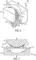
- FIG. 6 is a perspective depiction, and FIG. 7 is a cross section, of a portion of an article or structure 600 such as a replaceable component having a curved surface 602 to which a printed memory 100 is attached.
- the depictions of FIGS. 6 and 7 are during an initial physical (but not electrical) contact of the printed memory 100 with the wiring assembly 200, in preparation for a read cycle of the printed memory 100.
- the structure 600 and the wiring assembly 200 are brought in contact with each other, through movement of the structure 600, the reader 400, or both.
- a surface of the printed memory 100 on the curved surface 602 physically contacts the wiring assembly 200 between electrical contacts 210.
- the electrical contacts 210 and the contact pads 108 do not physically or electrically contact each other.
- wiring assembly 200 bends or flexes and begins to conform to the shape of the curved surface 602 of the structure 600.
- the electrical contacts 210 and the contact pads 108 physically and electrically contact each other and, as the wiring assembly 200 continues to flex, the electrical contacts 210 roll into place onto the contact pads 108, until the electrical contacts 210 and the contact pads 108 are in complete physical and electrical contact with each other.
- the wiring assembly 200 thus flexes from a first flat profile as depicted in FIG. 7 to a second curved profile as depicted in FIG. 9 . As depicted particularly in FIG.
- the back surface 302 of the wiring assembly 200 conforms to, and physically contacts, the surface 403 of the cradle 402 that defines the recess 404.
- a complete electrical pathway may extend, or can be formed, from and/or between the ferroelectric layer 106, to the wiring lines 104, to the contact pads 108, to the electrical contacts 210, to the traces 206, to the vias 300, to the connector 500 to the cable 502, and to the controller such as the host controller 1604 ( FIG. 16 ).
- the flexible and compliant wiring assembly 200 allows for electrical connection of the electrical contacts 210 to the contact pads 108 of the printed memory 100 in a direction generally perpendicular to the printed memory 100 without sliding the electrical contacts 210 across the contact pads 108, which could wear or damage the contact pads 108.
- the compliant wiring assembly 200 wraps around the curved shape of the structure 600 and the printed memory 100 attached thereto as physical and electrical contact is made to the printed memory 100. In contrast, electrical contacts of a permanently curved wiring assembly would slide across the contact pads 108 of the printed memory 100, thereby contributing to wear and possible damage of the contact pads 108.
- the reader 400 of FIGS. 4-9 and more particularly the wiring assembly 200 of the reader 400, physically contacts the printed memory 100 when at least one of the wiring assembly 200 and the printed memory 100 is moving in a generally perpendicular direction toward the other.
- FIG. 10 depicts a part of a reader 1000, including wiring assembly 200 as described herein and a cradle 1002.
- the cradle 1002 includes a surface 1004 such as a curved surface that defines a recess 1006.
- the cradle 1002 can further include an angled surface 1007 that intersects the curved surface 1004 at an incline or oblique angle, for example, at an angle of from about 10° to about 75°, or from about 15° to about 60°. Inclusion of the optional angled surface 1007 may reduce wear of the back surface 302 of the wiring assembly 200 and/or may guide the wiring assembly 200 more precisely onto the curved surface 1004.
- the angled surface 1007 can thus control the motion of the wiring assembly 200 into the curved surface 1004 of the cradle 1002 to achieve a desired final position from a wider range of initial positions, or to make the transition from an initial position to a final position more smooth or gentle, thereby reducing wear and tear on the wiring assembly 200 and/or the cradle 1002.
- the angled surface 1007 can be, for example, a chamfer (i.e., a straight line or planar surface), a fillet (i.e., a circular or elliptical arc), or may have a specialized profile suitable for the specific device design.
- the back surface 302 of the wiring assembly 200 may slide across the angled surface 1007 and onto the curved surface 1004.
- the back surface 302 of the wiring assembly 200 may be provided by the flexible low-friction backing 218 described above to further reduce wear of the wiring assembly 200 during one or more read operations of one or more printed memories 100 by the reader 1000.
- the cradle 1002 can include and define other features, such as a pair of opposing slots or channels (i.e., a first channel and a second channel) 1008, with one channel 1008 at each lateral side of the cradle 1002.
- FIG. 11 depicts the FIG. 10 device after attachment of the cradle 1002 and the wiring assembly 200 to an electrical connector 1100, where the electrical connector 1100 is electrically coupled to each of the electrical contacts 210 through the plurality conductive traces 206, for example, through the plurality of conductive vias 300 ( FIG. 3 ) or another technique.
- the electrical connector 1100 can include one or more pegs 406, where the one or more pegs 406 provide a similar attachment and alignment function as described with reference to FIG. 4 . It will be appreciated that, in FIG. 4 , the pegs 406 are inserted through holes 220 in a direction from the back surface 302 of the wiring assembly 200, while in FIG. 11 the pegs are inserted through holes 220 in a direction from the front surface 304 of the wiring assembly 200.
- the electrical connector 1100 can be electrically coupled to a cable, such as cable 502 ( FIG. 5 ), where the cable provides similar functionality to cable 502 (not depicted in FIG. 11 for simplicity).
- the electrical connector 1100 includes a pair of opposing tabs (i.e., a first tab and a second tab) 1102, where each tab 1102 is inserted into, received by, and configured to slide back and forth along, one of the channels 1008. As the tabs 1102 slide back and forth within the channels 1008, the electrical connector 1100 slides back and forth within the recess 1006. Additionally, because the wiring assembly 200 is attached to the electrical connector 1100, the wiring assembly 200 can also slide back and forth within the recess 1006 defined by the curved surface 1004.
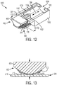
- FIG. 12 is a perspective depiction
- FIG. 13 is a cross section along 13-13 of FIG. 12 , of a portion of a structure 600 such as a replaceable component, for example, a toner bottle, having a curved surface 602 to which a printed memory 100 is attached.
- the depictions of FIGS. 12 and 13 are during an initial physical (but not electrical) contact of the printed memory 100 with the wiring assembly 200.
- the tabs 1102 are slid within the channels 1008 from a first end 1201 toward a second end 1202 opposite the first end 1201 of the cradle 1002.
- the cradle 1002 remains stationary while the structure 600, the electrical connector 1100, and the wiring assembly 200 attached to the electrical connector 1100 are moved toward the opposite end 1202 of the cradle 1002.
- the structure 600, the electrical connector 1100, and the wiring assembly 200 attached to the electrical connector 1100 remain stationary while the cradle 1002 is moved toward the structure 600 as the tabs 1102 slide within the channels 1008.
- both the cradle 1002 and the assembly including the structure 600, the wiring assembly 200, and the electrical connector 1100 are moved toward each other.
- FIGS. 14 and 15 depict the structures of FIGS. 12 and 13 after the plurality of electrical contacts 210 of the wiring assembly 200 physically and electrically contact the plurality of contact pads 108 of the printed memory 100.
- the tabs 1102 slide within the channels 1008 from the position of FIG. 12 to the position of FIG. 14
- the back surface 302 of the wiring assembly 200 slides across the angled surface 1007 and onto the curved surface 1004.
- at least a portion of the structure 600 is positioned within the recess 1006.
- the wiring assembly 200 bends, flexes, and/or conforms to the curved surface 1004 and wraps around the printed memory 100 such that the electrical contacts 210 physically and electrically contact the contact pads 108.
- the electrical contacts 210 physically contact the contact pads 108 without sliding across the contact pads 108, which would otherwise accelerate wear and possible damage of the contact pads 108.
- the wiring assembly 200 thus flexes from a first flat profile as depicted in FIG. 13 to a second curved profile as depicted in FIG. 15 .
- FIG. 16 is a schematic depiction of an example host device 1600 in an implementation of the present teachings.
- a host device 1600 can include other features and/or structures that are not depicted for simplicity, while various depicted features and/or structures can be removed or modified.
- the host device 1600 can be or include, for example, a printer or another electronic device that can include a replaceable component 1602, for example, a customer replaceable component such as a toner cartridge, an ink cartridge, a fuser, or another printer part.
- Other fields that may benefit from an implementation to reduce or prevent counterfeiting, or for other uses, include industries such as cosmetics, comestibles, pharmaceuticals, filters, reagents, medical devices, interchangeable heads or other interchangeable parts for electronic devices or other tools, etc.
- Circuitry within and/or electrically coupled to the host device 1600 can include a host controller 1604, a security module 1606, a printed memory reader 1608 (e.g., a reader 400, 1000 described herein or another reader), and a printed memory 1610 (e.g., printed memory 100 as described herein or another authentication circuit) attached to the replaceable component 1602.
- the host controller 1604 instructs the security module 1606 to perform a read operation of the printed memory 1610 on the replaceable component 1602.
- the read operation can include electrically coupling the printed memory reader 1608 with the printed memory 1610 as described herein, for example, using the wiring assembly 200.
- the security module 1606 compares data read from the printed memory 1610 using the printed memory reader 1608 to expected data from, for example, a lookup table stored in the security module 1606. If the read data matches the expected data, the security module 1606 instructs the host controller 1604 to enable functionality of the host device 1600. If the read data does not match the expected data, the security module 1606 instructs the host controller 1604 to disable functionality of the host device 1600.
- a reader in accordance with the present teachings may be an electrical device reader that is used to read and/or write and/or monitor and/or perform another operation on or from an electrical device other than printed memory, for example, for use during a transfer of data to and/or from an integrated circuit, a logic device, a microprocessor, other types of memory devices, a printed circuit board, etc., through the wiring assembly 200.
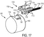
- FIGS. 17-19 depict another implementation of a wiring assembly 1700 that conforms to a shape of an article or structure 600 such as a replaceable component having a curved surface 602 to which a printed memory 100 is attached.
- the wiring assembly 1700 can include a flexible substrate 1706 that includes a rigid first portion 1708 and a rigid second portion 1710 configured to cooperatively engage the printed memory 100 with a plurality of electrical contacts 1712, for example, spring-loaded electrical contacts. While this implementation is described relative to two rigid portions, a wiring assembly having a flexible substrate that includes more than two rigid portions is contemplated.
- Each electrical contact 1712 of the plurality of electrical contacts 1712 can be directly electrically coupled with one or more electrical connectors 1714, or can be electrically coupled using electrically conductive traces (not individually depicted for simplicity).
- the electrical connectors 1714 can be electrically coupled to, for example, a security module 1606 ( FIG. 16 ) through one or more cables 1716.
- the wiring assembly 1700 can be mounted to a shaft 1718 that positions the wiring assembly 1700 within the host device 1600 ( FIG. 16 ).
- the structure 600 Upon positioning the structure 600 within the host device 1600, the structure 600, and more particularly the printed memory 100 positioned on the structure 600, can be aligned with the wiring assembly 1700 using any suitable technique such that the electrical contacts 1712 of the wiring assembly 1700 are positioned relative to the contact pads 108 of the printed circuit 100.
- one or more alignment grooves 1720 defined by the structure 600 can mate with one or more contours 1722 of the wiring assembly 1700 as depicted in FIG. 18 to align the electrical contacts 1712 with the contact pads 108.
- FIG. 17 further depicts a positioner 1724 (e.g., a spring) that elastically maintains the first portion 1708 and the second portion 1710 of the wiring assembly 1700 in a first position depicted in FIGS. 17 and 18 , but allows the wiring assembly 1700 to be repositioned into a second position depicted in FIG. 19 as discussed below.
- a positioner 1724 e.g., a spring
- the wiring assembly 1700 can engage with a driver mechanism 1900 which repositions the flexible substrate 1706 from the first position as depicted in FIG. 18 to the second position as depicted in FIG. 19 .
- the driver mechanism 1900 includes a pair of guides that engage with the first portion 1708 and second portion 1710 of the flexible substrate 1706 during or after the positioning of the structure 600.
- Other driver mechanisms for example, electromechanical driver mechanisms, are contemplated.
- the flexible substrate 1706 pivots and articulates about a pivot point provided by the shaft 1718 to provide the flexible substrate of the wiring assembly 1700.
- the wiring assembly 1700 thus flexes and/or articulates from a first profile "P 1 " as depicted in FIG. 18 to a second profile "P 2 " as depicted in FIG. 19 , where the second profile is different from the first profile.
- the flexible substrate 1706 including the first portion 1708 and the second portion 1710, is thus configured as a flexible substrate that supports the electrical contacts 1712.
- profile P 1 defines an angle greater than 180° while in FIG. 19 profile P 2 defines an angle less than 180°, although other implementations are contemplated.
- the electrical contacts 1712 physically and electrically contact the contact pads 108 of the printed memory, and thus the wiring assembly 1700 can be used to perform a memory operation on the printed memory 100.
- the driver mechanism 1900 can release the first portion 1708 and second portion 1710 of the wiring assembly 1700, and the positioner 1724 repositions the wiring assembly 1700 into the first position of FIG. 17 . This can occur, for example, when the structure 600 is removed from the host device 1600 by a user, or at any other desired time after performing the memory operation.
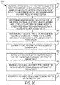
- a process or method 2000 for authenticating a replaceable component of a host device is depicted in the flow chart of FIG. 20 .
- the method 2000 can proceed by operation or use of one or more of the structures depicted in the figures described above, and thus is described with reference to one or more of the previous figures; however, it will be appreciated that the method 2000 is not limited to any particular structure or use unless expressly stated herein. It will be appreciated that while the method 2000 is described as a series of acts or events, the present teachings are not limited by the ordering of such acts or events. Some acts can occur in different orders and/or concurrently with other acts or events apart from those described herein. Further, a method in accordance with the present teachings can include other acts or events that have not been depicted for simplicity, while other illustrated acts or events can be removed or modified.
- a wiring assembly 200, 1700 in a first position can be positioned adjacent to a curved printed memory 100, wherein electrical contacts 210, 1712 of the wiring assembly 200, 1700 do not electrically couple with the contact pads 108 of the printed memory as at 2002. Further, in the first position, the wiring assembly has a first profile (see, for example, FIGS. 6, 7 , 12, 13 , and 18 ).
- the wiring assembly 200, 1700 is repositioned into a second position, wherein the electrical contacts 210, 1712 of the wiring assembly 200, 1700 are electrically coupled with the contact pads 108 of the curved printed memory 100 and the wiring assembly 200, 1700 has a second profile in the second position (see, for example, FIGS. 8, 9 , 14, 15 , 18 ).
- data can be read from the printed memory 100. It will be appreciated that in other implementations, a different memory operation can be performed exclusive of, or in addition to, the read operation of the printed memory 100.
- the data read from the printed memory can be compared to expected data, for example, using the security module 1606, the host controller 1604, or another component of the host device 1600 ( FIG. 16 ), as at 2008.
- functionality of the host device 1600 can be enabled, for example, by or using the security module 1606.
- functionality of the host device 1600 can be disabled, for example, by or using the security module 1606.
- the wiring assembly 200, 1700 can be repositioned from the second position to the first position as at 2014.
- a reader in accordance with the present teachings may be used with any electrical device such as an electrical device including a removable or consumable object, wherein the electrical device electrically connects to the reader at a plurality of contact points and sliding contact is undesirable.
- the reader is particularly useful when contact pads of a device being read, written, monitored, etc., can be worn and/or damaged by a sliding contact with contact pads, probes, pins, etc., of a reader. This can occur, for example, in a device design when the contact pads are part of, or positioned on, or positioned as, a curved surface, as well as in other device designs.
- the wiring assembly has a first profile when electrical contacts of the wiring assembly are not electrically coupled to contact pads of an electrical device, and the wiring assembly has a second profile that is different than the first profile when the electrical contacts of the wiring assembly are electrically coupled to contact pads of the electrical device.
- the wiring assembly may have a first profile that is other than flat, such as curved in a first direction or by a first amount.
- the wiring assembly may have a second profile that is different than the first profile, such as curved in a second direction that is different than the first direction, or curved by a second amount that is different than the first amount.
- the first and/or second profiles can be other than curved or flat, such as doubly curved or some other configuration.
- "curved" can include any shape of a surface not constrained to planar, including cylindrical, piecewise planar, varying curvature, multiply curved shapes such as double-curved shapes, etc.
- the numerical values as stated for the parameter can take on negative values.
- the example value of range stated as "less than 10" can assume negative values, e.g. - 1, -2, -3, -10, -20, -30, etc.
- one or more of the acts depicted herein may be carried out in one or more separate acts and/or phases.
- the terms “including,” “includes,” “having,” “has,” “with,” or variants thereof are used in either the detailed description and the claims, such terms are intended to be inclusive in a manner similar to the term “comprising.”
- the term “at least one of” is used to mean one or more of the listed items can be selected.
- the term “one or more of” with respect to a listing of items such as, for example, A and B, means A alone, B alone, or A and B.
- the term “on” used with respect to two materials, one “on” the other, means at least some contact between the materials, while “over” means the materials are in proximity, but possibly with one or more additional intervening materials such that contact is possible but not required. Neither “on” nor “over” implies any directionality as used herein.
- the term “conformal” describes a coating material in which angles of the underlying material are preserved by the conformal material. The term “about” indicates that the value listed may be somewhat altered, as long as the alteration does not result in nonconformance of the process or structure to the illustrated implementation. Finally, "exemplary” indicates the description is used as an example, rather than implying that it is an ideal.
- Terms of relative position as used in this application are defined based on a plane parallel to the conventional plane or working surface of a workpiece, regardless of the orientation of the workpiece.
- the term “horizontal” or “lateral” as used in this application is defined as a plane parallel to the conventional plane or working surface of a workpiece, regardless of the orientation of the workpiece.
- the term “vertical” refers to a direction perpendicular to the horizontal. Terms such as “on,” “side” (as in “sidewall”), “higher,” “lower,” “over,” “top,” and “under” are defined with respect to the conventional plane or working surface being on the top surface of the workpiece, regardless of the orientation of the workpiece.
Landscapes
- Engineering & Computer Science (AREA)
- Physics & Mathematics (AREA)
- Theoretical Computer Science (AREA)
- General Physics & Mathematics (AREA)
- Artificial Intelligence (AREA)
- Computer Vision & Pattern Recognition (AREA)
- Microelectronics & Electronic Packaging (AREA)
- Health & Medical Sciences (AREA)
- Toxicology (AREA)
- Computer Hardware Design (AREA)
- Electromagnetism (AREA)
- General Health & Medical Sciences (AREA)
- Computer Security & Cryptography (AREA)
- Software Systems (AREA)
- General Engineering & Computer Science (AREA)
- Coupling Device And Connection With Printed Circuit (AREA)
- Accessory Devices And Overall Control Thereof (AREA)
- Electrophotography Configuration And Component (AREA)
Abstract
Description
- The present teachings relate to the field of memory devices and product marking, for example, products including a tag or label for authentication and/or inventory control and, more particularly, to readers and scanners for reading and/or writing data from/to a product marked with an electronic memory, tag, or label.
- Xerox Printed Memory is a highly secure printed label including rewritable memory. In one exemplary use, the labels may be used for authentication to determine whether a product is authentic or genuine to prevent counterfeiting. For example, the printed memory may be attached as a label onto a subassembly of a customer-replaceable unit such as various consumable components, supplies, shipment packaging, consumer products, documents, etc. Data from the printed memory may be read, for example, after installation of the unit to which it is attached into a host device and compared to an expected result or value. If the value read from the printed memory matches the expected value, circuitry within the host device allows the host device to function. If the value read from the printed memory does not match the expected value, the circuitry disables functionality of the host device until an authentic or genuine unit is installed.
- In another implementation, Xerox Printed Memory may be used to track a product through a manufacturing process and/or a supply chain. The labels can be programmed to mark individual items with a unique electronic identifier that may be verified with a scanner. Other uses for Xerox Printed Memory are contemplated including, but not limited to, smart consumables where an object is associated with data that is later used by a base unit to improve or optimize performance, consumption records where bulk usage of a product supply is tracked, tracking of items or people outside of a manufacturing environment, etc.
- A Xerox Printed Memory includes a layer of ferroelectric or ferrite material (i.e., a ferroelectric layer) positioned between a plurality of wiring lines (e.g., word lines and bit lines). A region of the ferroelectric layer situated between each bit line and word line forms a memory cell. The memory may be written with one of two digital memory states by applying a suitable write voltage to the wiring lines. The memory state may be read by applying a suitable read voltage to the wiring lines through electrical contacts (e.g., landings or landing pads).
- Various manufacturing processes may be used to form the ferroelectric material. Depending on the manufacturing process used, the printed memory device will display particular electrical characteristics. For example, for a given read voltage, different compositions of the ferroelectric layer return different output values. The manufacture and composition of the memory itself is difficult to counterfeit and provides secure and reliable anti-counterfeiting measures and reliable product tracking.
- The following presents a simplified summary in order to provide a basic understanding of some aspects of one or more implementations of the present teachings. This summary is not an extensive overview, nor is it intended to identify key or critical elements of the present teachings, nor to delineate the scope of the disclosure. Rather, its primary purpose is merely to present one or more concepts in simplified form as a prelude to the detailed description presented later.
- An electrical device reader according to an implementation of the present teachings can include a wiring assembly having a flexible substrate and a plurality of electrical contacts supported by the flexible substrate. The device reader can further include an electrical connector electrically coupled with the plurality of electrical contacts, wherein the wiring assembly is configured to flex from a first profile in which the plurality of electrical contacts are not electrically coupled with a plurality of contact pads of an electrical device into a second profile in which the plurality of electrical contacts are electrically coupled with the plurality of contact pads of the electrical device.
- Optionally, the first profile can be a flat profile and the second profile can be a curved profile. The electrical device reader can further include a cradle positioned relative to the electrical connector and having a curved surface that defines a recess in the cradle, wherein the wiring assembly is configured to flex and conform to the curved surface of the cradle into a curved profile during a transfer of data from and/or to an electrical device through the wiring assembly. The cradle can define a first channel and a second channel and the electrical connector can include a first tab and a second tab, where the first tab is positioned within the first channel, the second tab is positioned within the second channel, and the first and second tabs are configured to slide within the first and second channels. The electrical connector can be configured to slide back and forth within the recess defined by the curved surface of the cradle.
- The flexible substrate can include a flexible underlayer, wherein the flexible underlayer includes one or more of a synthetic foam, a urethane foam, a urethane foam rubber, and felt.
- In an implementation, the electrical connector can include a first carriage and a second carriage, the cradle can include a first slot and a second slot, and the first and second carriages can be positioned within the first and second slots, thereby constraining movement of the electrical connector relative to the cradle along a path.
- The flexible substrate can include a rigid first portion and at least a rigid second portion, and the rigid first portion and the rigid second portion can be configured to articulate between a first position having the first profile and a second position having the second profile. The electrical device can further include a positioner that elastically maintains the wiring assembly in the first position having the first profile. The plurality of electrical contacts can include a plurality of spring-loaded electrical contacts. The electrical device reader can further include a driver mechanism configured to reposition the wiring assembly from the first position to the second position.
- The electronic device reader described above can be part of an electronic device, wherein the electronic device further includes a replaceable component having a curved surface and an electrical device attached to the curved surface of the replaceable component and having a curved profile. The wiring assembly of the electronic device reader can be configured to flex from a first profile in which the plurality of electrical contacts are not electrically coupled with a plurality of contact pads of the electrical device into a second profile in which the plurality of electrical contacts are electrically coupled with the plurality of contact pads of the electrical device.
- A method for authenticating a replaceable component of a host device can include positioning a wiring assembly in a first position adjacent to a curved printed memory, wherein a plurality of electrical contacts of the wiring assembly do not electrically couple with a plurality of contact pads of the curved printed memory, and the wiring assembly has a first profile in the first position and repositioning the wiring assembly into a second position, wherein the plurality of electrical contacts of the wiring assembly are electrically coupled with the plurality of contact pads of the curved printed memory and the wiring assembly has a second profile in the second position. Further, with the plurality of contact pads electrically coupled to the plurality of electrical contacts, data can be read from the curved printed memory. The method can further include comparing the data read from the curved printed memory to expected data. Responsive to the data read from the curved printed memory matching the expected data, functionality of the host device can be enabled and, responsive to the data read from the curved printed memory not matching the expected data, functionality of the host device can be disabled.
- The repositioning of the wiring assembly into the second position can include flexing a flexible underlayer of the wiring assembly from a flat profile to a curved profile.
- The repositioning of the wiring assembly into the second position can include articulating a rigid first portion of the wiring assembly and at least a second rigid second portion of the wiring assembly between the first position and the second position, and can further include engaging the rigid first portion and the rigid second portion with a driver mechanism thereby repositioning the rigid first portion and the rigid second portion from the first position to the second position and repositioning the wiring assembly from the second position into the first position using a positioner that elastically maintains the rigid first portion and the rigid second portion in the first position.
-
FIG. 1 is a plan view of a memory device, for example, a printed memory such as a Xerox Printed Memory. -
FIG. 2 is a perspective depiction of a wiring assembly according to an implementation of the present teachings. -
FIG. 3 is a cross section of theFIG. 2 wiring assembly. -
FIG. 4 is a perspective depiction of a portion of a reader in accordance with an implementation of the present teachings. -
FIG. 5 is another perspective depiction of theFIG. 4 structure. -
FIG. 6 is a perspective depiction of the reader ofFIG. 4 in preparation for a read of a printed memory device attached to a structure. -
FIG. 7 is a cross section of theFIG. 6 device. -
FIG. 8 is a perspective depiction of theFIG. 6 device where the printed memory and reader are positioned for a read operation. -
FIG. 9 is a cross section of theFIG. 8 device. -
FIG. 10 is a perspective depiction of a reader portion in accordance with another implementation of the present teachings. -
FIG. 11 . is a perspective depiction of theFIG. 10 device, further including an electrical connector. -
FIG. 12 is a perspective depiction of theFIG. 11 device in preparation for a read of a printed memory device attached to a structure. -
FIG. 13 is a cross section of theFIG. 12 device. -
FIG. 14 is a perspective depiction of theFIG. 11 device where the printed memory and reader are positioned for a read operation. -
FIG. 15 is a cross section of theFIG. 14 device. -
FIG. 16 is a schematic depiction of a host device including a reader in accordance with an implementation of the present teachings. -
FIG. 17 is a perspective depiction of another implementation of the present teachings. -
FIG. 18 is an end view of theFIG. 17 structure in a first position. -
FIG. 19 is an end view of theFIG. 17 structure in a second position. -
FIG. 20 is a flow chart depicting a method for authenticating a replaceable component in a host device. - As used herein, "data" refers to any type of information, signals, or results that are obtained from or sent to an electrical device such as a memory device, an integrated circuit, or another electrical device, or any information obtained from monitoring, interrogating, querying, or measuring, etc., an electrical device. The term "data" includes digital data, analog data, voltage values, current values, resistance values, vector values, scalar values, and/or flux values.
- An example of a
memory device 100, for example, a printed memory (printed memory device) 100 such as a Xerox PrintedMemory 100 is depicted in the plan view ofFIG. 1 . The structure and function of the Xerox PrintedMemory 100 is known, and is only briefly discussed herein. TheFIG. 1 printedmemory 100 includes asubstrate 102, for example, a flexibledielectric substrate 102, such as a flexible polymer substrate, that may include an adhesive backing layer to aid in attachment of the printedmemory 100 to a surface of a product, a plurality of wiring lines (e.g., word lines and bit lines) 104 and a ferroelectric layer 106 directly interposed or positioned between the word lines and the bit lines. A memory cell that stores the logic bit or logic state is provided by and within the ferroelectric layer 106 at the physical location that is interposed between the intersection of each word line and bit line. It will thus be appreciated that the word lines and bit lines do not physically intersect, but are physically separated by the ferroelectric layer 106. The printedmemory 100 depicted inFIG. 1 includes 10 wiring lines 104 (five word lines and five bit lines), and thus theFIG. 1 device includes 25 memory cells and may thus store 25 bits of information. Eachwiring line 104 terminates in acontact pad 108. It will be appreciated that a Xerox Printed Memory may include other structures that are not described or depicted for simplicity, while various depicted structures may be removed or modified. Each memory cell of the printedmemory 100 may be read by applying a suitable read voltage to two of the wiring lines 104 (i.e., to one word line and one bit line) and measuring an electrical response. To apply the read voltage, the plurality ofcontact pads 108 can be physically and electrically contacted with probe contacts of a reader. A voltage is applied across thecontact pads 108 through probe contacts, and the resulting response is measured. Each memory cell may individually addressed during a read or write cycle, and two or more, or all, of the memory cells in the memory array may be read or written simultaneously or serially. - The
contact pads 108 of the printedmemory 100 and other electrical devices can be formed using a carbon-impregnated composite, electrically conductive inks such as silver nanoparticle ink, or one or more other suitable materials. When thecontact pads 108 are provided on a flat, planar, or near-planar surface, the probe contacts of the reader can be placed into physical contact with thecontact pads 108 in a direction that is perpendicular to the plane of thecontact pads 108, thereby minimizing wear or scratching from the physical contact. However, being physically flexible, the printedmemory 100 may be placed onto arcuate or curved surfaces. Physically contacting thecontact pads 108 with probe pads when the printedmemory 100 is placed onto a curved surface can result in accelerated wear of thecontact pads 108 as the probe contacts slide into place across and ontocontact pads 108. The rate of wear and/or scratching may be increased as the radius of the curved surface to which the printedmemory 100 is attached decreases, for example, because the smaller radius results in a smaller contact area and thus larger contact pressure or contact stress. - An implementation of the present teachings provides a reader that may be used with printed
memory 100, such as Xerox PrintedMemory 100, or another memory device or electrical device. The reader can be a standalone device such as a handheld reader, or can be integrated as a subsystem of another electronic host device such as a printer. In one implementation, the printedmemory 100 can be placed onto a curved surface, such as an exterior surface of a toner bottle, and used as a toner bottle anti-counterfeiting measure. The printedmemory 100 can be read by the reader, where the reader is a subsystem of the printer to confirm that an installed toner bottle is genuine (e.g., is not a counterfeit or a gray market product). A controller and circuitry within the printer can enable printer functionality if the toner bottle is determined to be genuine, or can disable printer functionality if the toner bottle is determined to be counterfeit or gray market. -
FIGS. 2-9 depict various reader components in accordance with an implementation of the present teachings. While the figures depict various structures and features of a possible implementation of the present teachings, it will be appreciated that this or other designs may include other structures and/or features that are not depicted, while various depicted structures and/or features may be removed or modified. -
FIG. 2 is a perspective depiction, andFIG. 3 is a cross section along 3-3 ofFIG. 2 , of awiring assembly 200, such as a printed wiring assembly, for a reader in accordance with an implementation of the present teachings. Thewiring assembly 200 includes aflexible circuit 202 that includes asubstrate 204 and a plurality of electrically conductive interconnects or traces 206 formed on thesubstrate 204. Thesubstrate 204 is a flexible electrically insulative material, for example, a polymer such as a polyimide. Thetraces 206 can be or include an electrically conductive material such as a metal, a metal alloy, a conductive ink, etc. - A first end of each
trace 206 can terminate a contact pad (e.g., a first contact pad) 208 having anelectrical contact 210 formed thereon that will make physical and electrical contact with thecontact pads 108 of the printedmemory 100. Eachelectrical contact 210 can be or include, for example, a conductive bump formed at least partially from a solder material, a metal-filled epoxy, or another electrically conductive material. etc. In another implementation, eachelectrical contact 210 can be or include a spring-loaded connector, a probe tip, an anisotropic elastomeric interconnect, or another type ofelectrical contact 210. - A second end of each
trace 206 opposite the first end can also terminate a contact pad (e.g., a second contact pad) 212. The second end of each trace can be electrically coupled to an electrically conductive stud or via 300 at an underside of eachcontact pad 212. The conductive via 300 extends from the underside of the of thecontact pad 212 to aback surface 302 of thewiring assembly 200 as depicted inFIG. 3 and facilitates the electrical coupling of eachcontact pad 212 with a connector and cable as described below. As depicted inFIG. 3 , theback surface 302 of thewiring assembly 200 is opposite afront surface 304, where thefront surface 304 includestraces 206. - The
wiring assembly 200 can further include a flexible substrate orflexible underlayer 216 attached to, and supporting, theflexible circuit 202 including theelectrical contacts 210. In an implementation, theflexible underlayer 216 can include a foam layer or polymer core layer that bends, flexes, or is compliant when placed under pressure. Theflexible underlayer 216 can be or include a synthetic material, for example, a synthetic foam such as a urethane foam or a urethane foam rubber, or another material such as felt or another natural or synthetic flexible material. Theconductive vias 300 can traverse through openings in theflexible underlayer 216 and extend from aback surface 302 of thewiring assembly 200 as depicted inFIG. 3 . In another implementation, electrical connectors can be incorporated with an articulated flexible circuit having spring-loaded or telescoping electrical contacts, where the articulated flexible circuit conforms to a shape of a structure to which the printedmemory 100 is attached, for example, as discussed below relative toFIGS. 17-19 . - The
wiring assembly 200 can optionally include abacking 218 such as a flexible, low-friction backing that provides low sliding friction and added wear resistance to theback surface 302 of thewiring assembly 200 during use of the reader as described below. As used herein, a "low-friction" backing 218 refers to a structure where a coefficient of friction of the material of thebacking 218 is less than a coefficient of friction of the material of theflexible underlayer 216. Thebacking 218 can be or include a synthetic material such as a polyamide film or polyethylene terephthalate film, for example a nylon film or a Mylar® film, having a thickness of from about 0.002 inches (0.05 millimeters) to about 0.025 inches (0.6 millimeters). Thebacking 218 may contribute to a stiffness of thewiring assembly 200. Thewiring assembly 200 may be excessively stiff if thebacking 218 is too thick. Insufficient thickness of thebacking 218 may lead to failure of the backing during use if the backing is worn through by physical contact with thecradle 402 or is otherwise damaged through contact with thecradle 402 in such a way as to impair its function. - Additionally, the
wiring assembly 200 can include one or more optional mounting features that assist in mounting and/or aligning thewiring assembly 200 to an electrical connector as described below. For example, thewiring assembly 200 can include one or more mountingholes 220 as mounting features, although other types of mounting features and techniques for mounting the electrical connector to thewiring assembly 200 are contemplated. - In addition to the
wiring assembly 200, thereader 400 can further include acradle 402 that may be attached to, or otherwise positioned adjacent to, thewiring assembly 200 as depicted in the perspective depictions ofFIGS. 4 and5 . In this implementation, thecradle 402 includes asurface 403 such as a curved surface that defines arecess 404 having a shape that is suitable to receive the structure to which the printedmemory 100 is attached. In this non-limiting example implementation, the printedmemory 100 is attached to an exterior convex surface of a toner bottle having a radius, and thus thesurface 403 and therecess 404 defined thereby has a concave shape as depicted, with a radius that is suitable to receive the surface of the toner bottle. - As depicted in
FIGS. 4 and5 , thereader 400 can also include aconnector 500, such as an electrical connector, physically and/or electrically attached to and/or integrated with thewiring assembly 200. In some implementations, theconnector 500 can be physically connected to thecradle 402 such that it is moveably attached to thecradle 402, such as slidably attached to thecradle 402, or theconnector 500 can be fixedly attached to thecradle 402. Theconnector 500 may be constrained to move in a particular way relative to thecradle 402. In particular, theconnector 500 may be constrained to slide along a path relative to thecradle 402. Theconnector 500 can be electrically coupled to each via 300 of the plurality ofvias 300. Additionally, theconnector 500 may be electrically coupled to acable 502 that is used to route electrical signals, data, or other information between the printedmemory 100 and other reader circuitry, such as a host controller 1604 (FIG. 16 ), during use as described below. In an implementation, the connector may include a mass-produced and/or commercially available connector positioned within a custom housing such as a custom plastic housing. - To facilitate alignment between the
connector 500 and thecradle 402, theconnector 500 can include one or more arms orcarriages 504 that are received byslots 506 defined by thecradle 402 as depicted inFIG. 5 , where thecarriages 504 are positioned within theslots 506.FIG. 5 depicts first andsecond carriages 504 and first andsecond slots 506. Theslots 506 are shaped to position thecarriages 504, and thus theconnector 500, relative to thecradle 402. Furthermore, theconnector 500 may include one ormore pegs 406 such as heat stakes received by the mountingholes 220 as depicted inFIG. 4 , which mount thewiring assembly 200 onto theconnector 500 and thecradle 402, and position thecircuit assembly 200 relative to thecradle 402. Thepegs 406 can be offset from the printedmemory 100 and the structure to which the printedmemory 100 is attached. In another implementation, thepegs 406 can be, include, or be functionally replaced by, one or more rivets, screws, adhesives, etc. In another implementation, eachpeg 406 may extend into a recess (not depicted for simplicity) in the structure to which the printedmemory 100 is attached. Thecradle 402 can includealignment tabs 408 that also assist to laterally position thewiring assembly 200 on thecradle 402. Theback surface 302 of thewiring assembly 200 can rest on afront face 410 of thecradle 402. -
FIG. 6 is a perspective depiction, andFIG. 7 is a cross section, of a portion of an article orstructure 600 such as a replaceable component having acurved surface 602 to which a printedmemory 100 is attached. The depictions ofFIGS. 6 and 7 are during an initial physical (but not electrical) contact of the printedmemory 100 with thewiring assembly 200, in preparation for a read cycle of the printedmemory 100. As depicted inFIG. 7 , thestructure 600 and thewiring assembly 200 are brought in contact with each other, through movement of thestructure 600, thereader 400, or both. As thestructure 600 and thewiring assembly 200 are brought together, a surface of the printedmemory 100 on thecurved surface 602 physically contacts thewiring assembly 200 betweenelectrical contacts 210. At this point, theelectrical contacts 210 and thecontact pads 108 do not physically or electrically contact each other. As thestructure 600 and thewiring assembly 200 continue to be brought together, wiringassembly 200 bends or flexes and begins to conform to the shape of thecurved surface 602 of thestructure 600. Theelectrical contacts 210 and thecontact pads 108 physically and electrically contact each other and, as thewiring assembly 200 continues to flex, theelectrical contacts 210 roll into place onto thecontact pads 108, until theelectrical contacts 210 and thecontact pads 108 are in complete physical and electrical contact with each other. Thewiring assembly 200 thus flexes from a first flat profile as depicted inFIG. 7 to a second curved profile as depicted inFIG. 9 . As depicted particularly inFIG. 9 , theback surface 302 of thewiring assembly 200 conforms to, and physically contacts, thesurface 403 of thecradle 402 that defines therecess 404. Once a predetermined compressive force is applied between thestructure 600 and thereader 400, and more particularly between thecontact pads 108 of the printedmemory 100 and theelectrical contacts 210 of the wiring assembly 200 (i.e., generally, a compressive force in the direction of the arrows depicted inFIG. 7 ), a memory operation such as a read operation can be performed on the printedmemory 100. Once electrical connection is established between thecontact pads 108 and theelectrical contacts 210, a complete electrical pathway may extend, or can be formed, from and/or between the ferroelectric layer 106, to thewiring lines 104, to thecontact pads 108, to theelectrical contacts 210, to thetraces 206, to thevias 300, to theconnector 500 to thecable 502, and to the controller such as the host controller 1604 (FIG. 16 ). - The flexible and
compliant wiring assembly 200 allows for electrical connection of theelectrical contacts 210 to thecontact pads 108 of the printedmemory 100 in a direction generally perpendicular to the printedmemory 100 without sliding theelectrical contacts 210 across thecontact pads 108, which could wear or damage thecontact pads 108. Thecompliant wiring assembly 200 wraps around the curved shape of thestructure 600 and the printedmemory 100 attached thereto as physical and electrical contact is made to the printedmemory 100. In contrast, electrical contacts of a permanently curved wiring assembly would slide across thecontact pads 108 of the printedmemory 100, thereby contributing to wear and possible damage of thecontact pads 108. - The
reader 400 ofFIGS. 4-9 , and more particularly thewiring assembly 200 of thereader 400, physically contacts the printedmemory 100 when at least one of thewiring assembly 200 and the printedmemory 100 is moving in a generally perpendicular direction toward the other. - Another implementation of the present teachings is depicted in
FIGS. 10-15 .FIG. 10 depicts a part of areader 1000, includingwiring assembly 200 as described herein and acradle 1002. Thecradle 1002 includes asurface 1004 such as a curved surface that defines arecess 1006. Thecradle 1002 can further include anangled surface 1007 that intersects thecurved surface 1004 at an incline or oblique angle, for example, at an angle of from about 10° to about 75°, or from about 15° to about 60°. Inclusion of the optionalangled surface 1007 may reduce wear of theback surface 302 of thewiring assembly 200 and/or may guide thewiring assembly 200 more precisely onto thecurved surface 1004. Theangled surface 1007 can thus control the motion of thewiring assembly 200 into thecurved surface 1004 of thecradle 1002 to achieve a desired final position from a wider range of initial positions, or to make the transition from an initial position to a final position more smooth or gentle, thereby reducing wear and tear on thewiring assembly 200 and/or thecradle 1002. It will be appreciated that theangled surface 1007 can be, for example, a chamfer (i.e., a straight line or planar surface), a fillet (i.e., a circular or elliptical arc), or may have a specialized profile suitable for the specific device design. During use of thereader 1000, theback surface 302 of thewiring assembly 200 may slide across theangled surface 1007 and onto thecurved surface 1004. In this implementation, theback surface 302 of thewiring assembly 200 may be provided by the flexible low-friction backing 218 described above to further reduce wear of thewiring assembly 200 during one or more read operations of one or more printedmemories 100 by thereader 1000. Thecradle 1002 can include and define other features, such as a pair of opposing slots or channels (i.e., a first channel and a second channel) 1008, with onechannel 1008 at each lateral side of thecradle 1002. -
FIG. 11 depicts theFIG. 10 device after attachment of thecradle 1002 and thewiring assembly 200 to anelectrical connector 1100, where theelectrical connector 1100 is electrically coupled to each of theelectrical contacts 210 through the plurality conductive traces 206, for example, through the plurality of conductive vias 300 (FIG. 3 ) or another technique. Theelectrical connector 1100 can include one ormore pegs 406, where the one ormore pegs 406 provide a similar attachment and alignment function as described with reference toFIG. 4 . It will be appreciated that, inFIG. 4 , thepegs 406 are inserted throughholes 220 in a direction from theback surface 302 of thewiring assembly 200, while inFIG. 11 the pegs are inserted throughholes 220 in a direction from thefront surface 304 of thewiring assembly 200. - Further, the
electrical connector 1100 can be electrically coupled to a cable, such as cable 502 (FIG. 5 ), where the cable provides similar functionality to cable 502 (not depicted inFIG. 11 for simplicity). - As further depicted in
FIG. 11 , theelectrical connector 1100 includes a pair of opposing tabs (i.e., a first tab and a second tab) 1102, where eachtab 1102 is inserted into, received by, and configured to slide back and forth along, one of thechannels 1008. As thetabs 1102 slide back and forth within thechannels 1008, theelectrical connector 1100 slides back and forth within therecess 1006. Additionally, because thewiring assembly 200 is attached to theelectrical connector 1100, thewiring assembly 200 can also slide back and forth within therecess 1006 defined by thecurved surface 1004. -
FIG. 12 is a perspective depiction, andFIG. 13 is a cross section along 13-13 ofFIG. 12 , of a portion of astructure 600 such as a replaceable component, for example, a toner bottle, having acurved surface 602 to which a printedmemory 100 is attached. The depictions ofFIGS. 12 and 13 are during an initial physical (but not electrical) contact of the printedmemory 100 with thewiring assembly 200. Once thestructure 600 andwiring assembly 200 are positioned relative to each other as depicted inFIGS. 12 and 13 , thetabs 1102 are slid within thechannels 1008 from afirst end 1201 toward asecond end 1202 opposite thefirst end 1201 of thecradle 1002. In one implementation, thecradle 1002 remains stationary while thestructure 600, theelectrical connector 1100, and thewiring assembly 200 attached to theelectrical connector 1100 are moved toward theopposite end 1202 of thecradle 1002. In another implementation, thestructure 600, theelectrical connector 1100, and thewiring assembly 200 attached to theelectrical connector 1100 remain stationary while thecradle 1002 is moved toward thestructure 600 as thetabs 1102 slide within thechannels 1008. In yet another implementation, both thecradle 1002 and the assembly including thestructure 600, thewiring assembly 200, and theelectrical connector 1100, are moved toward each other. -
FIGS. 14 and 15 depict the structures ofFIGS. 12 and 13 after the plurality ofelectrical contacts 210 of thewiring assembly 200 physically and electrically contact the plurality ofcontact pads 108 of the printedmemory 100. As thetabs 1102 slide within thechannels 1008 from the position ofFIG. 12 to the position ofFIG. 14 , theback surface 302 of thewiring assembly 200 slides across theangled surface 1007 and onto thecurved surface 1004. Simultaneously, at least a portion of thestructure 600 is positioned within therecess 1006. As theback surface 302 slides onto thecurved surface 1004, thewiring assembly 200 bends, flexes, and/or conforms to thecurved surface 1004 and wraps around the printedmemory 100 such that theelectrical contacts 210 physically and electrically contact thecontact pads 108. Thus theelectrical contacts 210 physically contact thecontact pads 108 without sliding across thecontact pads 108, which would otherwise accelerate wear and possible damage of thecontact pads 108. Thewiring assembly 200 thus flexes from a first flat profile as depicted inFIG. 13 to a second curved profile as depicted inFIG. 15 . - In the implementation of
FIGS. 10-15 , when thewiring assembly 200 and the printedmemory 100 are moving relative to thecradle 1002, the surface of the printedmemory 100 having thecontact pads 108 moves in a direction parallel to a direction of movement of thefront surface 304 of thewiring assembly 200. -
FIG. 16 is a schematic depiction of anexample host device 1600 in an implementation of the present teachings. It will be appreciated that ahost device 1600 can include other features and/or structures that are not depicted for simplicity, while various depicted features and/or structures can be removed or modified. Thehost device 1600 can be or include, for example, a printer or another electronic device that can include areplaceable component 1602, for example, a customer replaceable component such as a toner cartridge, an ink cartridge, a fuser, or another printer part. Other fields that may benefit from an implementation to reduce or prevent counterfeiting, or for other uses, include industries such as cosmetics, comestibles, pharmaceuticals, filters, reagents, medical devices, interchangeable heads or other interchangeable parts for electronic devices or other tools, etc. Circuitry within and/or electrically coupled to thehost device 1600 can include ahost controller 1604, asecurity module 1606, a printed memory reader 1608 (e.g., areader memory 100 as described herein or another authentication circuit) attached to thereplaceable component 1602. In an implementation, upon an installation of thereplaceable component 1602 and powering on thehost device 1600, thehost controller 1604 instructs thesecurity module 1606 to perform a read operation of the printedmemory 1610 on thereplaceable component 1602. The read operation can include electrically coupling the printedmemory reader 1608 with the printedmemory 1610 as described herein, for example, using thewiring assembly 200. Thesecurity module 1606 compares data read from the printedmemory 1610 using the printedmemory reader 1608 to expected data from, for example, a lookup table stored in thesecurity module 1606. If the read data matches the expected data, thesecurity module 1606 instructs thehost controller 1604 to enable functionality of thehost device 1600. If the read data does not match the expected data, thesecurity module 1606 instructs thehost controller 1604 to disable functionality of thehost device 1600. - It will be appreciated that the
security module 1606 may enable or disable device functionality directly, and that other operational methods resulting in the same or similar outcomes are contemplated. It will also be appreciated that while the present teachings are discussed for illustration purposes relative to a read operation of a printed memory, a reader in accordance with the present teachings may be an electrical device reader that is used to read and/or write and/or monitor and/or perform another operation on or from an electrical device other than printed memory, for example, for use during a transfer of data to and/or from an integrated circuit, a logic device, a microprocessor, other types of memory devices, a printed circuit board, etc., through thewiring assembly 200. -
FIGS. 17-19 depict another implementation of awiring assembly 1700 that conforms to a shape of an article orstructure 600 such as a replaceable component having acurved surface 602 to which a printedmemory 100 is attached. Thewiring assembly 1700 can include aflexible substrate 1706 that includes a rigidfirst portion 1708 and a rigidsecond portion 1710 configured to cooperatively engage the printedmemory 100 with a plurality ofelectrical contacts 1712, for example, spring-loaded electrical contacts. While this implementation is described relative to two rigid portions, a wiring assembly having a flexible substrate that includes more than two rigid portions is contemplated. Eachelectrical contact 1712 of the plurality ofelectrical contacts 1712 can be directly electrically coupled with one or moreelectrical connectors 1714, or can be electrically coupled using electrically conductive traces (not individually depicted for simplicity). Theelectrical connectors 1714 can be electrically coupled to, for example, a security module 1606 (FIG. 16 ) through one ormore cables 1716. - The
wiring assembly 1700 can be mounted to ashaft 1718 that positions thewiring assembly 1700 within the host device 1600 (FIG. 16 ). Upon positioning thestructure 600 within thehost device 1600, thestructure 600, and more particularly the printedmemory 100 positioned on thestructure 600, can be aligned with thewiring assembly 1700 using any suitable technique such that theelectrical contacts 1712 of thewiring assembly 1700 are positioned relative to thecontact pads 108 of the printedcircuit 100. In one implementation, for example, one ormore alignment grooves 1720 defined by thestructure 600 can mate with one ormore contours 1722 of thewiring assembly 1700 as depicted inFIG. 18 to align theelectrical contacts 1712 with thecontact pads 108.FIG. 17 further depicts a positioner 1724 (e.g., a spring) that elastically maintains thefirst portion 1708 and thesecond portion 1710 of thewiring assembly 1700 in a first position depicted inFIGS. 17 and18 , but allows thewiring assembly 1700 to be repositioned into a second position depicted inFIG. 19 as discussed below. - During or after the positioning and alignment of the printed
memory 100 with theelectrical contacts 1712 as depicted inFIG. 18 , thewiring assembly 1700, and more particularly thefirst portion 1708 andsecond portion 1710 of theflexible substrate 1706, can engage with adriver mechanism 1900 which repositions theflexible substrate 1706 from the first position as depicted inFIG. 18 to the second position as depicted inFIG. 19 . In this implementation, thedriver mechanism 1900 includes a pair of guides that engage with thefirst portion 1708 andsecond portion 1710 of theflexible substrate 1706 during or after the positioning of thestructure 600. Other driver mechanisms, for example, electromechanical driver mechanisms, are contemplated. During the repositioning, theflexible substrate 1706 pivots and articulates about a pivot point provided by theshaft 1718 to provide the flexible substrate of thewiring assembly 1700. Thewiring assembly 1700 thus flexes and/or articulates from a first profile "P1" as depicted inFIG. 18 to a second profile "P2" as depicted inFIG. 19 , where the second profile is different from the first profile. Theflexible substrate 1706, including thefirst portion 1708 and thesecond portion 1710, is thus configured as a flexible substrate that supports theelectrical contacts 1712. InFIG. 18 , profile P1 defines an angle greater than 180° while inFIG. 19 profile P2 defines an angle less than 180°, although other implementations are contemplated. When in theFIG. 19 position, theelectrical contacts 1712 physically and electrically contact thecontact pads 108 of the printed memory, and thus thewiring assembly 1700 can be used to perform a memory operation on the printedmemory 100. - After performing the memory operation, the
driver mechanism 1900 can release thefirst portion 1708 andsecond portion 1710 of thewiring assembly 1700, and thepositioner 1724 repositions thewiring assembly 1700 into the first position ofFIG. 17 . This can occur, for example, when thestructure 600 is removed from thehost device 1600 by a user, or at any other desired time after performing the memory operation. - A process or
method 2000 for authenticating a replaceable component of a host device is depicted in the flow chart ofFIG. 20 . Themethod 2000 can proceed by operation or use of one or more of the structures depicted in the figures described above, and thus is described with reference to one or more of the previous figures; however, it will be appreciated that themethod 2000 is not limited to any particular structure or use unless expressly stated herein. It will be appreciated that while themethod 2000 is described as a series of acts or events, the present teachings are not limited by the ordering of such acts or events. Some acts can occur in different orders and/or concurrently with other acts or events apart from those described herein. Further, a method in accordance with the present teachings can include other acts or events that have not been depicted for simplicity, while other illustrated acts or events can be removed or modified. - In an implementation of the
method 2000 for authenticating areplaceable component 600 of ahost device 1600, awiring assembly memory 100, whereinelectrical contacts wiring assembly contact pads 108 of the printed memory as at 2002. Further, in the first position, the wiring assembly has a first profile (see, for example,FIGS. 6, 7 ,12, 13 , and18 ). Next, at 2004, thewiring assembly electrical contacts wiring assembly contact pads 108 of the curved printedmemory 100 and thewiring assembly FIGS. 8, 9 ,14, 15 ,18 ). At 2006, with the plurality ofcontact pads 108 of the printedmemory 100 electrically coupled to the plurality ofelectrical contacts wiring assembly memory 100. It will be appreciated that in other implementations, a different memory operation can be performed exclusive of, or in addition to, the read operation of the printedmemory 100. - Next, the data read from the printed memory can be compared to expected data, for example, using the
security module 1606, thehost controller 1604, or another component of the host device 1600 (FIG. 16 ), as at 2008. At 2010, responsive to the data read matching the expected data, functionality of thehost device 1600 can be enabled, for example, by or using thesecurity module 1606. At 2012, responsive to the data read not matching the expected data, functionality of thehost device 1600 can be disabled, for example, by or using thesecurity module 1606. During themethod 1700, thewiring assembly - It will be appreciated that while the present teachings are discussed with regard to a reader for performing a memory operation on a printed memory that may be attached to a curved surface, other uses are contemplated. For example, a reader in accordance with the present teachings may be used with any electrical device such as an electrical device including a removable or consumable object, wherein the electrical device electrically connects to the reader at a plurality of contact points and sliding contact is undesirable. Without limiting, the reader is particularly useful when contact pads of a device being read, written, monitored, etc., can be worn and/or damaged by a sliding contact with contact pads, probes, pins, etc., of a reader. This can occur, for example, in a device design when the contact pads are part of, or positioned on, or positioned as, a curved surface, as well as in other device designs.
- It will be further appreciated that while the present teachings are discussed relative to a wiring assembly having a flat profile being flexed into a curved profile, other implementations of the present teachings are contemplated. Generally, the wiring assembly has a first profile when electrical contacts of the wiring assembly are not electrically coupled to contact pads of an electrical device, and the wiring assembly has a second profile that is different than the first profile when the electrical contacts of the wiring assembly are electrically coupled to contact pads of the electrical device. In a natural, unflexed, free, or unconnected state, the wiring assembly may have a first profile that is other than flat, such as curved in a first direction or by a first amount. In a flexed, bent, or connected state, the wiring assembly may have a second profile that is different than the first profile, such as curved in a second direction that is different than the first direction, or curved by a second amount that is different than the first amount. The first and/or second profiles can be other than curved or flat, such as doubly curved or some other configuration. Additionally, "curved" can include any shape of a surface not constrained to planar, including cylindrical, piecewise planar, varying curvature, multiply curved shapes such as double-curved shapes, etc.
- Notwithstanding that the numerical ranges and parameters setting forth the broad scope of the present teachings are approximations, the numerical values set forth in the specific examples are reported as precisely as possible. Any numerical value, however, inherently contains certain errors necessarily resulting from the standard deviation found in their respective testing measurements. Moreover, all ranges disclosed herein are to be understood to encompass any and all sub-ranges subsumed therein. For example, a range of "less than 10" can include any and all sub-ranges between (and including) the minimum value of zero and the maximum value of 10, that is, any and all sub-ranges having a minimum value of equal to or greater than zero and a maximum value of equal to or less than 10, e.g., 1 to 5. In certain cases, the numerical values as stated for the parameter can take on negative values. In this case, the example value of range stated as "less than 10" can assume negative values, e.g. - 1, -2, -3, -10, -20, -30, etc.
- While the present teachings have been illustrated with respect to one or more implementations, alterations and/or modifications can be made to the illustrated examples without departing from the spirit and scope of the appended claims. For example, it will be appreciated that while the process is described as a series of acts or events, the present teachings are not limited by the ordering of such acts or events. Some acts may occur in different orders and/or concurrently with other acts or events apart from those described herein. Also, not all process stages may be required to implement a methodology in accordance with one or more aspects or implementations of the present teachings. It will be appreciated that structural components and/or processing stages can be added or existing structural components and/or processing stages can be removed or modified. Further, one or more of the acts depicted herein may be carried out in one or more separate acts and/or phases. Furthermore, to the extent that the terms "including," "includes," "having," "has," "with," or variants thereof are used in either the detailed description and the claims, such terms are intended to be inclusive in a manner similar to the term "comprising." The term "at least one of" is used to mean one or more of the listed items can be selected. As used herein, the term "one or more of" with respect to a listing of items such as, for example, A and B, means A alone, B alone, or A and B. Further, in the discussion and claims herein, the term "on" used with respect to two materials, one "on" the other, means at least some contact between the materials, while "over" means the materials are in proximity, but possibly with one or more additional intervening materials such that contact is possible but not required. Neither "on" nor "over" implies any directionality as used herein. The term "conformal" describes a coating material in which angles of the underlying material are preserved by the conformal material. The term "about" indicates that the value listed may be somewhat altered, as long as the alteration does not result in nonconformance of the process or structure to the illustrated implementation. Finally, "exemplary" indicates the description is used as an example, rather than implying that it is an ideal. Other implementations of the present teachings will be apparent to those skilled in the art from consideration of the specification and practice of the disclosure herein. It is intended that the specification and examples be considered as exemplary only, with a true scope and spirit of the present teachings being indicated by the following claims.
- Terms of relative position as used in this application are defined based on a plane parallel to the conventional plane or working surface of a workpiece, regardless of the orientation of the workpiece. The term "horizontal" or "lateral" as used in this application is defined as a plane parallel to the conventional plane or working surface of a workpiece, regardless of the orientation of the workpiece. The term "vertical" refers to a direction perpendicular to the horizontal. Terms such as "on," "side" (as in "sidewall"), "higher," "lower," "over," "top," and "under" are defined with respect to the conventional plane or working surface being on the top surface of the workpiece, regardless of the orientation of the workpiece.
Claims (20)
- An electrical device reader, comprising:a wiring assembly, comprising:a flexible substrate; anda plurality of electrical contacts supported by the flexible substrate; andan electrical connector electrically coupled with the plurality of electrical contacts,wherein the wiring assembly is configured to flex from a first profile in which the plurality of electrical contacts are not electrically coupled with a plurality of contact pads of an electrical device into a second profile in which the plurality of electrical contacts are electrically coupled with the plurality of contact pads of the electrical device.
- The electrical device reader of claim 1, wherein the first profile is a flat profile and the second profile is a curved profile.
- The electrical device reader of claim 1, further comprising a cradle positioned relative to the electrical connector and comprising a curved surface that defines a recess in the cradle, wherein the wiring assembly is configured to flex and conform to the curved surface of the cradle into a curved profile during a transfer of data from and/or to an electrical device through the wiring assembly.
- The electrical device reader of claim 3, wherein:the cradle defines a first channel and a second channel;the electrical connector comprises a first tab and a second tab;the first tab is positioned within the first channel;the second tab is positioned within the second channel; andthe first and second tabs are configured to slide within the first and second channels.
- The electrical device reader of claim 4, wherein the electrical connector is configured to slide back and forth within the recess defined by the curved surface of the cradle.
- The electrical device reader of claim 3, wherein the flexible substrate comprises a flexible underlayer, wherein the flexible underlayer includes one or more of a synthetic foam, a urethane foam, a urethane foam rubber, and felt.
- The electrical device reader of claim 3, wherein:the electrical connector comprises a first carriage and a second carriage;the cradle comprises a first slot and a second slot; andthe first and second carriages are positioned within the first and second slots, thereby constraining movement of the electrical connector relative to the cradle along a path.
- The electrical device reader of claim 1, wherein:the flexible substrate comprises a rigid first portion and at least a rigid second portion; andthe rigid first portion and the rigid second portion are configured to articulate between a first position having the first profile and a second position having the second profile.
- The electrical device reader of claim 8, further comprising a positioner that elastically maintains the wiring assembly in the first position having the first profile.
- The electrical device reader of claim 8, wherein the plurality of electrical contacts comprise a plurality of spring-loaded electrical contacts.
- The electrical device reader of claim 10, further comprising a driver mechanism configured to reposition the wiring assembly from the first position to the second position.
- An electronic device, comprising:a replaceable component comprising a curved surface;an electrical device attached to the curved surface of the replaceable component and having a curved profile; andan electrical device reader, comprising:a wiring assembly, comprising:a flexible substrate; anda plurality of electrical contacts supported by the flexible substrate; andan electrical connector electrically coupled with the plurality of electrical contacts,wherein the wiring assembly is configured to flex from a first profile in which the plurality of electrical contacts are not electrically coupled with a plurality of contact pads of the electrical device into a second profile in which the plurality of electrical contacts are electrically coupled with the plurality of contact pads of the electrical device.
- The electronic device of claim 12, the electrical device reader further comprising a cradle positioned relative to the electrical connector and comprising a curved surface that defines a recess in the cradle, wherein the wiring assembly is configured to flex and conform to the curved surface of the cradle into a curved profile during a transfer of data from and/or to an electrical device through the wiring assembly.
- The electronic device of claim 13, wherein:the first profile is a flat profile and the second profile is a curved profile the cradle defines a first channel and a second channel;the electrical connector comprises a first tab and a second tab;the first tab is positioned within the first channel;the second tab is positioned within the second channel; andthe first and second tabs are configured to slide within the first and second channels.
- The electronic device of claim 12, wherein:the flexible substrate comprises a rigid first portion and at least a rigid second portion; andthe rigid first portion and the rigid second portion are configured to articulate between a first position having the first profile and a second position having the second profile.
- The electronic device of claim 15, wherein the electrical device reader further comprises:a positioner that elastically maintains the wiring assembly in the first position having the first profile; anda driver mechanism configured to reposition the wiring assembly from the first position to the second position,wherein the plurality of electrical contacts comprise a plurality of spring-loaded electrical contacts.
- A method for authenticating a replaceable component of a host device, comprising:positioning a wiring assembly in a first position adjacent to a curved printed memory, wherein a plurality of electrical contacts of the wiring assembly do not electrically couple with a plurality of contact pads of the curved printed memory, and the wiring assembly has a first profile in the first position;repositioning the wiring assembly into a second position, wherein the plurality of electrical contacts of the wiring assembly are electrically coupled with the plurality of contact pads of the curved printed memory and the wiring assembly has a second profile in the second position;with the plurality of contact pads electrically coupled to the plurality of electrical contacts, reading data from the curved printed memory;comparing the data read from the curved printed memory to expected data;responsive to the data read from the curved printed memory matching the expected data, enabling functionality of the host device; andresponsive to the data read from the curved printed memory not matching the expected data, disabling functionality of the host device.
- The method of claim 17, wherein the repositioning of the wiring assembly into the second position comprises flexing a flexible underlayer of the wiring assembly from a flat profile to a curved profile.
- The method of claim 17, wherein the repositioning of the wiring assembly into the second position comprises articulating a rigid first portion of the wiring assembly and at least a rigid second portion of the wiring assembly between the first position and the second position.
- The method of claim 19, further comprising:engaging the rigid first portion and the rigid second portion with a driver mechanism thereby repositioning the rigid first portion and the rigid second portion from the first position to the second position; andrepositioning the wiring assembly from the second position into the first position using a positioner that elastically maintains the rigid first portion and the rigid second portion in the first position.
Applications Claiming Priority (1)
| Application Number | Priority Date | Filing Date | Title |
|---|---|---|---|
| US15/987,784 US10797421B2 (en) | 2018-05-23 | 2018-05-23 | Landing electrical contact |
Publications (2)
| Publication Number | Publication Date |
|---|---|
| EP3572969A1 true EP3572969A1 (en) | 2019-11-27 |
| EP3572969B1 EP3572969B1 (en) | 2021-11-24 |
Family
ID=66625771
Family Applications (1)
| Application Number | Title | Priority Date | Filing Date |
|---|---|---|---|
| EP19175265.8A Active EP3572969B1 (en) | 2018-05-23 | 2019-05-17 | Landing electrical contact |
Country Status (5)
| Country | Link |
|---|---|
| US (1) | US10797421B2 (en) |
| EP (1) | EP3572969B1 (en) |
| JP (1) | JP7327884B2 (en) |
| KR (1) | KR102451210B1 (en) |
| CN (1) | CN110532821B (en) |
Families Citing this family (2)
| Publication number | Priority date | Publication date | Assignee | Title |
|---|---|---|---|---|
| US10796212B2 (en) | 2018-10-02 | 2020-10-06 | Xerox Corporation | Orientation-agnostic method to interface to printed memory label |
| WO2020073206A1 (en) * | 2018-10-09 | 2020-04-16 | 华为技术有限公司 | Chip, method for generating private key, and method for trusted verification |
Citations (2)
| Publication number | Priority date | Publication date | Assignee | Title |
|---|---|---|---|---|
| US5583445A (en) * | 1994-02-04 | 1996-12-10 | Hughes Aircraft Company | Opto-electronic membrane probe |
| US9934415B1 (en) * | 2017-04-20 | 2018-04-03 | Xerox Corporation | Handheld reader having transparent circuit board for alignment of multiple electrical contacts |
Family Cites Families (14)
| Publication number | Priority date | Publication date | Assignee | Title |
|---|---|---|---|---|
| US20070206364A1 (en) * | 2006-03-02 | 2007-09-06 | Saint-Gobain Performance Plastics Corporation | Methods of forming a flexible circuit board |
| JP4947637B2 (en) * | 2007-01-09 | 2012-06-06 | ソニーモバイルコミュニケーションズ株式会社 | Non-contact power transmission coil, portable terminal and terminal charging device |
| FR2944625B1 (en) * | 2009-04-15 | 2012-03-09 | Ingenico Sa | MEMORY CARD READER. |
| US8981796B2 (en) * | 2010-04-30 | 2015-03-17 | Cynetic Designs Ltd. | Wireless method and apparatus for detecting damage in ceramic body armor |
| US8559830B2 (en) * | 2011-05-11 | 2013-10-15 | Xerox Corporation | Lockout device and an indicator to ensure that the correct consumable is replaced in a printing device |
| US8584331B2 (en) * | 2011-09-14 | 2013-11-19 | Xerox Corporation | In situ flexible circuit embossing to form an electrical interconnect |
| US9024891B2 (en) * | 2011-11-03 | 2015-05-05 | Synaptics Incorporated | Single substrate touch sensor |
| US9293851B2 (en) * | 2013-03-15 | 2016-03-22 | Nike, Inc. | Electronic connector having flexible region |
| US9433349B2 (en) * | 2013-07-17 | 2016-09-06 | General Electric Company | Surface stationary array coil structure for multi-modality imaging |
| US20160072554A1 (en) * | 2014-09-08 | 2016-03-10 | Aliphcom | Near-field antennas and methods of implementing the same for wearable pods and devices that include metalized interfaces |
| US9886571B2 (en) | 2016-02-16 | 2018-02-06 | Xerox Corporation | Security enhancement of customer replaceable unit monitor (CRUM) |
| US9933906B2 (en) * | 2016-03-28 | 2018-04-03 | Synaptics Incorporated | Capacitive sensing using discrete lighting elements |
| KR102473658B1 (en) * | 2016-05-27 | 2022-12-02 | 삼성전자주식회사 | Semiconductor device |
| KR102590307B1 (en) * | 2016-08-30 | 2023-10-16 | 엘지디스플레이 주식회사 | Flexible display device and method of manufacturing the same |
-
2018
- 2018-05-23 US US15/987,784 patent/US10797421B2/en active Active
-
2019
- 2019-04-25 JP JP2019083815A patent/JP7327884B2/en active Active
- 2019-04-25 CN CN201910336295.2A patent/CN110532821B/en active Active
- 2019-05-07 KR KR1020190052814A patent/KR102451210B1/en active Active
- 2019-05-17 EP EP19175265.8A patent/EP3572969B1/en active Active
Patent Citations (2)
| Publication number | Priority date | Publication date | Assignee | Title |
|---|---|---|---|---|
| US5583445A (en) * | 1994-02-04 | 1996-12-10 | Hughes Aircraft Company | Opto-electronic membrane probe |
| US9934415B1 (en) * | 2017-04-20 | 2018-04-03 | Xerox Corporation | Handheld reader having transparent circuit board for alignment of multiple electrical contacts |
Also Published As
| Publication number | Publication date |
|---|---|
| US20190363471A1 (en) | 2019-11-28 |
| JP2019204501A (en) | 2019-11-28 |
| US10797421B2 (en) | 2020-10-06 |
| CN110532821A (en) | 2019-12-03 |
| CN110532821B (en) | 2022-04-05 |
| JP7327884B2 (en) | 2023-08-16 |
| KR20190133598A (en) | 2019-12-03 |
| EP3572969B1 (en) | 2021-11-24 |
| KR102451210B1 (en) | 2022-10-06 |
Similar Documents
| Publication | Publication Date | Title |
|---|---|---|
| EP3572969B1 (en) | Landing electrical contact | |
| US20170068833A1 (en) | Radio frequency identification system | |
| JP5352006B2 (en) | Card device and socket | |
| US20070153426A1 (en) | Recording disk drive capable of suppressing vibration of flexible printed circuit board | |
| US8397997B2 (en) | Removable media spindle and antenna assembly for printer | |
| GB2387567A (en) | Ink cartridge and holder with positioning means | |
| EP1060895B1 (en) | A printer and method adapted to sense data of a consumable loaded into the printer | |
| US20130015959A1 (en) | Rfid tag issuing apparatus and rfid tag misalignment detecting method | |
| US8992105B2 (en) | Printing system ribbon including print transferable circuitry and elements | |
| US11106958B2 (en) | Orientation-agnostic method to interface to printed memory | |
| JP2016074542A (en) | Paper tray size sensing mechanism | |
| US6480356B1 (en) | Magnetic head transducer spring assembly and method of making same | |
| EP1416431A1 (en) | Docking station for writing to electronically writable display | |
| US6083771A (en) | Method and system for manufacturing theft-deterrent computer components | |
| US7621451B2 (en) | Radio frequency identification labels and systems and methods for making the same | |
| JP6258752B2 (en) | IC tag issuing device | |
| EP1760628B1 (en) | Magnetic head group, magnetic recording medium processing device and magnetic head-holding frame | |
| JP4689411B2 (en) | Magnetic head assembly, magnetic recording medium processing apparatus, and frame for holding magnetic head | |
| CN214027861U (en) | Portable Label Printer | |
| JP2004322496A (en) | Image forming apparatus and image forming method using the same | |
| CN114503223A (en) | System and method for identifying and marking cables in an industrial rack | |
| HK1125340A1 (en) | Circuit board | |
| HK1125340B (en) | Circuit board |
Legal Events
| Date | Code | Title | Description |
|---|---|---|---|
| PUAI | Public reference made under article 153(3) epc to a published international application that has entered the european phase |
Free format text: ORIGINAL CODE: 0009012 |
|
| STAA | Information on the status of an ep patent application or granted ep patent |
Free format text: STATUS: THE APPLICATION HAS BEEN PUBLISHED |
|
| AK | Designated contracting states |
Kind code of ref document: A1 Designated state(s): AL AT BE BG CH CY CZ DE DK EE ES FI FR GB GR HR HU IE IS IT LI LT LU LV MC MK MT NL NO PL PT RO RS SE SI SK SM TR |
|
| AX | Request for extension of the european patent |
Extension state: BA ME |
|
| STAA | Information on the status of an ep patent application or granted ep patent |
Free format text: STATUS: REQUEST FOR EXAMINATION WAS MADE |
|
| 17P | Request for examination filed |
Effective date: 20200527 |
|
| RBV | Designated contracting states (corrected) |
Designated state(s): AL AT BE BG CH CY CZ DE DK EE ES FI FR GB GR HR HU IE IS IT LI LT LU LV MC MK MT NL NO PL PT RO RS SE SI SK SM TR |
|
| GRAP | Despatch of communication of intention to grant a patent |
Free format text: ORIGINAL CODE: EPIDOSNIGR1 |
|
| STAA | Information on the status of an ep patent application or granted ep patent |
Free format text: STATUS: GRANT OF PATENT IS INTENDED |
|
| INTG | Intention to grant announced |
Effective date: 20210621 |
|
| GRAS | Grant fee paid |
Free format text: ORIGINAL CODE: EPIDOSNIGR3 |
|
| GRAA | (expected) grant |
Free format text: ORIGINAL CODE: 0009210 |
|
| STAA | Information on the status of an ep patent application or granted ep patent |
Free format text: STATUS: THE PATENT HAS BEEN GRANTED |
|
| AK | Designated contracting states |
Kind code of ref document: B1 Designated state(s): AL AT BE BG CH CY CZ DE DK EE ES FI FR GB GR HR HU IE IS IT LI LT LU LV MC MK MT NL NO PL PT RO RS SE SI SK SM TR |
|
| REG | Reference to a national code |
Ref country code: GB Ref legal event code: FG4D |
|
| REG | Reference to a national code |
Ref country code: AT Ref legal event code: REF Ref document number: 1450429 Country of ref document: AT Kind code of ref document: T Effective date: 20211215 |
|
| REG | Reference to a national code |
Ref country code: DE Ref legal event code: R096 Ref document number: 602019009456 Country of ref document: DE |
|
| REG | Reference to a national code |
Ref country code: IE Ref legal event code: FG4D |
|
| REG | Reference to a national code |
Ref country code: LT Ref legal event code: MG9D |
|
| REG | Reference to a national code |
Ref country code: NL Ref legal event code: MP Effective date: 20211124 |
|
| REG | Reference to a national code |
Ref country code: AT Ref legal event code: MK05 Ref document number: 1450429 Country of ref document: AT Kind code of ref document: T Effective date: 20211124 |
|
| PG25 | Lapsed in a contracting state [announced via postgrant information from national office to epo] |
Ref country code: RS Free format text: LAPSE BECAUSE OF FAILURE TO SUBMIT A TRANSLATION OF THE DESCRIPTION OR TO PAY THE FEE WITHIN THE PRESCRIBED TIME-LIMIT Effective date: 20211124 Ref country code: LT Free format text: LAPSE BECAUSE OF FAILURE TO SUBMIT A TRANSLATION OF THE DESCRIPTION OR TO PAY THE FEE WITHIN THE PRESCRIBED TIME-LIMIT Effective date: 20211124 Ref country code: FI Free format text: LAPSE BECAUSE OF FAILURE TO SUBMIT A TRANSLATION OF THE DESCRIPTION OR TO PAY THE FEE WITHIN THE PRESCRIBED TIME-LIMIT Effective date: 20211124 Ref country code: BG Free format text: LAPSE BECAUSE OF FAILURE TO SUBMIT A TRANSLATION OF THE DESCRIPTION OR TO PAY THE FEE WITHIN THE PRESCRIBED TIME-LIMIT Effective date: 20220224 Ref country code: AT Free format text: LAPSE BECAUSE OF FAILURE TO SUBMIT A TRANSLATION OF THE DESCRIPTION OR TO PAY THE FEE WITHIN THE PRESCRIBED TIME-LIMIT Effective date: 20211124 |
|
| PG25 | Lapsed in a contracting state [announced via postgrant information from national office to epo] |
Ref country code: IS Free format text: LAPSE BECAUSE OF FAILURE TO SUBMIT A TRANSLATION OF THE DESCRIPTION OR TO PAY THE FEE WITHIN THE PRESCRIBED TIME-LIMIT Effective date: 20220324 Ref country code: SE Free format text: LAPSE BECAUSE OF FAILURE TO SUBMIT A TRANSLATION OF THE DESCRIPTION OR TO PAY THE FEE WITHIN THE PRESCRIBED TIME-LIMIT Effective date: 20211124 Ref country code: PT Free format text: LAPSE BECAUSE OF FAILURE TO SUBMIT A TRANSLATION OF THE DESCRIPTION OR TO PAY THE FEE WITHIN THE PRESCRIBED TIME-LIMIT Effective date: 20220324 Ref country code: PL Free format text: LAPSE BECAUSE OF FAILURE TO SUBMIT A TRANSLATION OF THE DESCRIPTION OR TO PAY THE FEE WITHIN THE PRESCRIBED TIME-LIMIT Effective date: 20211124 Ref country code: NO Free format text: LAPSE BECAUSE OF FAILURE TO SUBMIT A TRANSLATION OF THE DESCRIPTION OR TO PAY THE FEE WITHIN THE PRESCRIBED TIME-LIMIT Effective date: 20220224 Ref country code: NL Free format text: LAPSE BECAUSE OF FAILURE TO SUBMIT A TRANSLATION OF THE DESCRIPTION OR TO PAY THE FEE WITHIN THE PRESCRIBED TIME-LIMIT Effective date: 20211124 Ref country code: LV Free format text: LAPSE BECAUSE OF FAILURE TO SUBMIT A TRANSLATION OF THE DESCRIPTION OR TO PAY THE FEE WITHIN THE PRESCRIBED TIME-LIMIT Effective date: 20211124 Ref country code: HR Free format text: LAPSE BECAUSE OF FAILURE TO SUBMIT A TRANSLATION OF THE DESCRIPTION OR TO PAY THE FEE WITHIN THE PRESCRIBED TIME-LIMIT Effective date: 20211124 Ref country code: GR Free format text: LAPSE BECAUSE OF FAILURE TO SUBMIT A TRANSLATION OF THE DESCRIPTION OR TO PAY THE FEE WITHIN THE PRESCRIBED TIME-LIMIT Effective date: 20220225 Ref country code: ES Free format text: LAPSE BECAUSE OF FAILURE TO SUBMIT A TRANSLATION OF THE DESCRIPTION OR TO PAY THE FEE WITHIN THE PRESCRIBED TIME-LIMIT Effective date: 20211124 |
|
| PG25 | Lapsed in a contracting state [announced via postgrant information from national office to epo] |
Ref country code: SM Free format text: LAPSE BECAUSE OF FAILURE TO SUBMIT A TRANSLATION OF THE DESCRIPTION OR TO PAY THE FEE WITHIN THE PRESCRIBED TIME-LIMIT Effective date: 20211124 Ref country code: SK Free format text: LAPSE BECAUSE OF FAILURE TO SUBMIT A TRANSLATION OF THE DESCRIPTION OR TO PAY THE FEE WITHIN THE PRESCRIBED TIME-LIMIT Effective date: 20211124 Ref country code: RO Free format text: LAPSE BECAUSE OF FAILURE TO SUBMIT A TRANSLATION OF THE DESCRIPTION OR TO PAY THE FEE WITHIN THE PRESCRIBED TIME-LIMIT Effective date: 20211124 Ref country code: EE Free format text: LAPSE BECAUSE OF FAILURE TO SUBMIT A TRANSLATION OF THE DESCRIPTION OR TO PAY THE FEE WITHIN THE PRESCRIBED TIME-LIMIT Effective date: 20211124 Ref country code: DK Free format text: LAPSE BECAUSE OF FAILURE TO SUBMIT A TRANSLATION OF THE DESCRIPTION OR TO PAY THE FEE WITHIN THE PRESCRIBED TIME-LIMIT Effective date: 20211124 Ref country code: CZ Free format text: LAPSE BECAUSE OF FAILURE TO SUBMIT A TRANSLATION OF THE DESCRIPTION OR TO PAY THE FEE WITHIN THE PRESCRIBED TIME-LIMIT Effective date: 20211124 |
|
| REG | Reference to a national code |
Ref country code: DE Ref legal event code: R097 Ref document number: 602019009456 Country of ref document: DE |
|
| PLBE | No opposition filed within time limit |
Free format text: ORIGINAL CODE: 0009261 |
|
| STAA | Information on the status of an ep patent application or granted ep patent |
Free format text: STATUS: NO OPPOSITION FILED WITHIN TIME LIMIT |
|
| PG25 | Lapsed in a contracting state [announced via postgrant information from national office to epo] |
Ref country code: AL Free format text: LAPSE BECAUSE OF FAILURE TO SUBMIT A TRANSLATION OF THE DESCRIPTION OR TO PAY THE FEE WITHIN THE PRESCRIBED TIME-LIMIT Effective date: 20211124 |
|
| 26N | No opposition filed |
Effective date: 20220825 |
|
| PG25 | Lapsed in a contracting state [announced via postgrant information from national office to epo] |
Ref country code: SI Free format text: LAPSE BECAUSE OF FAILURE TO SUBMIT A TRANSLATION OF THE DESCRIPTION OR TO PAY THE FEE WITHIN THE PRESCRIBED TIME-LIMIT Effective date: 20211124 |
|
| REG | Reference to a national code |
Ref country code: CH Ref legal event code: PL |
|
| REG | Reference to a national code |
Ref country code: BE Ref legal event code: MM Effective date: 20220531 |
|
| PG25 | Lapsed in a contracting state [announced via postgrant information from national office to epo] |
Ref country code: MC Free format text: LAPSE BECAUSE OF FAILURE TO SUBMIT A TRANSLATION OF THE DESCRIPTION OR TO PAY THE FEE WITHIN THE PRESCRIBED TIME-LIMIT Effective date: 20211124 Ref country code: LU Free format text: LAPSE BECAUSE OF NON-PAYMENT OF DUE FEES Effective date: 20220517 Ref country code: LI Free format text: LAPSE BECAUSE OF NON-PAYMENT OF DUE FEES Effective date: 20220531 Ref country code: CH Free format text: LAPSE BECAUSE OF NON-PAYMENT OF DUE FEES Effective date: 20220531 |
|
| PG25 | Lapsed in a contracting state [announced via postgrant information from national office to epo] |
Ref country code: IE Free format text: LAPSE BECAUSE OF NON-PAYMENT OF DUE FEES Effective date: 20220517 |
|
| PG25 | Lapsed in a contracting state [announced via postgrant information from national office to epo] |
Ref country code: IT Free format text: LAPSE BECAUSE OF FAILURE TO SUBMIT A TRANSLATION OF THE DESCRIPTION OR TO PAY THE FEE WITHIN THE PRESCRIBED TIME-LIMIT Effective date: 20211124 Ref country code: BE Free format text: LAPSE BECAUSE OF NON-PAYMENT OF DUE FEES Effective date: 20220531 |
|
| GBPC | Gb: european patent ceased through non-payment of renewal fee |
Effective date: 20230517 |
|
| PG25 | Lapsed in a contracting state [announced via postgrant information from national office to epo] |
Ref country code: HU Free format text: LAPSE BECAUSE OF FAILURE TO SUBMIT A TRANSLATION OF THE DESCRIPTION OR TO PAY THE FEE WITHIN THE PRESCRIBED TIME-LIMIT; INVALID AB INITIO Effective date: 20190517 |
|
| PG25 | Lapsed in a contracting state [announced via postgrant information from national office to epo] |
Ref country code: MK Free format text: LAPSE BECAUSE OF FAILURE TO SUBMIT A TRANSLATION OF THE DESCRIPTION OR TO PAY THE FEE WITHIN THE PRESCRIBED TIME-LIMIT Effective date: 20211124 Ref country code: CY Free format text: LAPSE BECAUSE OF FAILURE TO SUBMIT A TRANSLATION OF THE DESCRIPTION OR TO PAY THE FEE WITHIN THE PRESCRIBED TIME-LIMIT Effective date: 20211124 Ref country code: GB Free format text: LAPSE BECAUSE OF NON-PAYMENT OF DUE FEES Effective date: 20230517 |
|
| PG25 | Lapsed in a contracting state [announced via postgrant information from national office to epo] |
Ref country code: MT Free format text: LAPSE BECAUSE OF FAILURE TO SUBMIT A TRANSLATION OF THE DESCRIPTION OR TO PAY THE FEE WITHIN THE PRESCRIBED TIME-LIMIT Effective date: 20211124 |
|
| PGFP | Annual fee paid to national office [announced via postgrant information from national office to epo] |
Ref country code: DE Payment date: 20250423 Year of fee payment: 7 |
|
| PGFP | Annual fee paid to national office [announced via postgrant information from national office to epo] |
Ref country code: FR Payment date: 20250423 Year of fee payment: 7 |
|
| PG25 | Lapsed in a contracting state [announced via postgrant information from national office to epo] |
Ref country code: TR Free format text: LAPSE BECAUSE OF FAILURE TO SUBMIT A TRANSLATION OF THE DESCRIPTION OR TO PAY THE FEE WITHIN THE PRESCRIBED TIME-LIMIT Effective date: 20211124 |