EP3572968A1 - Clock gating unit for a transponder - Google Patents
Clock gating unit for a transponder Download PDFInfo
- Publication number
- EP3572968A1 EP3572968A1 EP18173666.1A EP18173666A EP3572968A1 EP 3572968 A1 EP3572968 A1 EP 3572968A1 EP 18173666 A EP18173666 A EP 18173666A EP 3572968 A1 EP3572968 A1 EP 3572968A1
- Authority
- EP
- European Patent Office
- Prior art keywords
- transponder
- data frame
- digital logic
- clock gating
- clock
- Prior art date
- Legal status (The legal status is an assumption and is not a legal conclusion. Google has not performed a legal analysis and makes no representation as to the accuracy of the status listed.)
- Granted
Links
Images


Classifications
-
- G—PHYSICS
- G06—COMPUTING OR CALCULATING; COUNTING
- G06K—GRAPHICAL DATA READING; PRESENTATION OF DATA; RECORD CARRIERS; HANDLING RECORD CARRIERS
- G06K19/00—Record carriers for use with machines and with at least a part designed to carry digital markings
- G06K19/06—Record carriers for use with machines and with at least a part designed to carry digital markings characterised by the kind of the digital marking, e.g. shape, nature, code
- G06K19/067—Record carriers with conductive marks, printed circuits or semiconductor circuit elements, e.g. credit or identity cards also with resonating or responding marks without active components
- G06K19/07—Record carriers with conductive marks, printed circuits or semiconductor circuit elements, e.g. credit or identity cards also with resonating or responding marks without active components with integrated circuit chips
- G06K19/0723—Record carriers with conductive marks, printed circuits or semiconductor circuit elements, e.g. credit or identity cards also with resonating or responding marks without active components with integrated circuit chips the record carrier comprising an arrangement for non-contact communication, e.g. wireless communication circuits on transponder cards, non-contact smart cards or RFIDs
-
- G—PHYSICS
- G06—COMPUTING OR CALCULATING; COUNTING
- G06F—ELECTRIC DIGITAL DATA PROCESSING
- G06F1/00—Details not covered by groups G06F3/00 - G06F13/00 and G06F21/00
- G06F1/26—Power supply means, e.g. regulation thereof
- G06F1/32—Means for saving power
- G06F1/3203—Power management, i.e. event-based initiation of a power-saving mode
- G06F1/3234—Power saving characterised by the action undertaken
- G06F1/3237—Power saving characterised by the action undertaken by disabling clock generation or distribution
-
- G—PHYSICS
- G06—COMPUTING OR CALCULATING; COUNTING
- G06F—ELECTRIC DIGITAL DATA PROCESSING
- G06F1/00—Details not covered by groups G06F3/00 - G06F13/00 and G06F21/00
- G06F1/26—Power supply means, e.g. regulation thereof
- G06F1/28—Supervision thereof, e.g. detecting power-supply failure by out of limits supervision
-
- G—PHYSICS
- G06—COMPUTING OR CALCULATING; COUNTING
- G06F—ELECTRIC DIGITAL DATA PROCESSING
- G06F1/00—Details not covered by groups G06F3/00 - G06F13/00 and G06F21/00
- G06F1/26—Power supply means, e.g. regulation thereof
- G06F1/30—Means for acting in the event of power-supply failure or interruption, e.g. power-supply fluctuations
- G06F1/305—Means for acting in the event of power-supply failure or interruption, e.g. power-supply fluctuations in the event of power-supply fluctuations
-
- G—PHYSICS
- G06—COMPUTING OR CALCULATING; COUNTING
- G06F—ELECTRIC DIGITAL DATA PROCESSING
- G06F1/00—Details not covered by groups G06F3/00 - G06F13/00 and G06F21/00
- G06F1/26—Power supply means, e.g. regulation thereof
- G06F1/32—Means for saving power
- G06F1/3203—Power management, i.e. event-based initiation of a power-saving mode
- G06F1/3206—Monitoring of events, devices or parameters that trigger a change in power modality
-
- G—PHYSICS
- G06—COMPUTING OR CALCULATING; COUNTING
- G06K—GRAPHICAL DATA READING; PRESENTATION OF DATA; RECORD CARRIERS; HANDLING RECORD CARRIERS
- G06K7/00—Methods or arrangements for sensing record carriers, e.g. for reading patterns
- G06K7/0008—General problems related to the reading of electronic memory record carriers, independent of its reading method, e.g. power transfer
-
- Y—GENERAL TAGGING OF NEW TECHNOLOGICAL DEVELOPMENTS; GENERAL TAGGING OF CROSS-SECTIONAL TECHNOLOGIES SPANNING OVER SEVERAL SECTIONS OF THE IPC; TECHNICAL SUBJECTS COVERED BY FORMER USPC CROSS-REFERENCE ART COLLECTIONS [XRACs] AND DIGESTS
- Y02—TECHNOLOGIES OR APPLICATIONS FOR MITIGATION OR ADAPTATION AGAINST CLIMATE CHANGE
- Y02D—CLIMATE CHANGE MITIGATION TECHNOLOGIES IN INFORMATION AND COMMUNICATION TECHNOLOGIES [ICT], I.E. INFORMATION AND COMMUNICATION TECHNOLOGIES AIMING AT THE REDUCTION OF THEIR OWN ENERGY USE
- Y02D10/00—Energy efficient computing, e.g. low power processors, power management or thermal management
Definitions
- the present disclosure relates to a transponder. Furthermore, the present disclosure relates to a method of operating a transponder, and to a corresponding computer program.
- a transponder such as a radio frequency identification (RFID) transponder, may receive commands from a reader and respond to those commands.
- RFID radio frequency identification
- the communication between the transponder and the reader may be susceptible to problems. For example, some commands may not be properly received or processed by the transponder. Similarly, some responses may not be properly received or processed by the reader.
- a transponder comprising: digital logic for processing one or more portions of a data frame; a status detection unit configured to detect a status of a data frame reception or data frame transmission; a clock gating unit configured to apply clock gating to said digital logic in dependence on the status of said data frame reception or data frame transmission.
- detecting the status of data frame reception comprises detecting an end of a Miller pause, and the clock gating unit is configured to apply said clock gating after said Miller pause.
- detecting the status of data frame transmission comprises detecting that the digital logic is active during the transmission of a response, and the clock gating unit is configured to apply said clock gating while the digital logic is active.
- detecting that the digital logic is active comprises detecting that the digital logic is copying response data to a transmission buffer.
- applying the clock gating comprises disabling the digital logic during a first predefined number of clock cycles and enabling the digital logic during a second predefined number of clock cycles.
- the first predefined number is one and the second predefined number is one; the first predefined number is two and the second predefined number is two; or the first predefined number is three and the second predefined number is one.
- disabling the digital logic and enabling the digital logic are repeated.
- the clock gating unit is further configured to apply said disabling and enabling for a predefined maximum number of clock cycles.
- the first predefined number of clock cycles, the second predefined number of clock cycles, and/or the predefined maximum number of clock cycles are programmable parameters.
- the transponder further comprises a memory for storing said programmable parameters.
- said memory is a non-volatile memory.
- the transponder is a radio frequency identification (RFID) transponder, in particular an RFID tag or an RFID card.
- RFID radio frequency identification
- a method of operating a transponder comprising: detecting, by a status detection unit of said transponder, a status of a data frame reception or data frame transmission; applying, by a clock gating unit of said transponder, clock gating to digital logic of said transponder in dependence on the status of said data frame reception or data frame transmission; processing, by said digital logic, one or more portions of a data frame.
- a computer program comprising instructions that, when executed by a processing unit, carry out a method of the kind set forth.
- a non-transitory computer-readable medium comprising a computer program of the kind set forth.
- RFID transponders are widely used, in different areas of industry and commerce and for various purposes.
- RFID transponders may for example be embodied as so-called RFID tags or RFID cards.
- NFC near field communication
- RFID transponders are regarded as a specific type of RFID transponders.
- the principles described herein may also be applied to NFC transponders.
- a transponder such as a radio frequency identification (RFID) transponder, may receive commands from a reader and respond to those commands.
- RFID radio frequency identification
- the communication between the transponder and the reader may be susceptible to problems. For example, some commands may not be properly received or processed by the transponder. Similarly, some responses may not be properly received or processed by the reader.
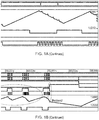
- Fig. 1A shows an example of an operation 100 of a transponder.
- a command is received by the transponder, it should be decoded, processed and a response should be transmitted back to the reader.
- a voltage sensor based mechanism can be used to gate clocks of most of the active digital logic momentarily to reduce power consumption and resume on voltage recovery. This is useful to avoid resets due to low voltage, particularly at lower field strengths. This is referred to as a clock-stop concept.
- the clock-stop concept or clock-stop feature enables achieving a higher distance of operation of the transponder from the reader (i.e. a lower minimal field strength H min ).
- Fig. 1 illustrates that a clock-stop is triggered ( vsens _ clkstop _ a _ o ) each time that the voltage drops below 1.8V ( vdda _ int ) .
- the digital logic clocks should be gated using vsens _ clkstop _ a _ o.
- vdda _ int denotes an internal signal that represents the operating voltage of the transponder.
- Fig. 1B shows another example of an operation 102 of a transponder.
- a reader communicates to a transponder a specific sequence of logical bits 0/1, which are amplitude modulated by the reader.
- This amplitude modulation of a created radio frequency (RF) field is referred to as a Miller pause in said technical standard ISO/IEC14443-2.
- RF radio frequency
- the transponder's digital logic (CPU subsystem) remains ungated after the Miller pause, in order to store (i.e. process) one or more bytes of the received command frame in a transponder memory.
- CPU subsystem the transponder's digital logic
- the demodulator of the tag may detect such a drop of voltage as a Miller pause. This, in turn, may result in a wrong Miller decoding and not responding to the command. This may predominantly be visible for higher baud rates such as 212 kbps, 424 kbps and 848 kbps, due to a lower demodulator sensitivity to detect lower Miller pause depths (for example modulation depths of 40%).
- Fig. 1B shows a simulation waveform with a command being received by the transponder ( dmod _ sync ) .
- the digital processing starts and consumes power causing a voltage drop ( vdda _ int ) .
- a traditional voltage sensor based clock-stop ( vsens _ clkstop _ a _ o ) is triggered after reaching a threshold voltage (1.8V). This clock-stop ( vsens _ clkstop _ a _ o ) gates the digital processing until the voltage is recovered ( vdda _ int ).
- a first problem is that the variation in voltage ( vdda _ int ) between Miller pauses may be detected by the demodulator of the transponder as a wrong Miller pause.
- a second problem is that the starting voltage ( vdda _ int ) at the start of the next Miller pause may drop due to the digital processing until the start of the next Miller pause; this may result in a higher minimum operating field strength (H min ) as it can trigger a low voltage reset (for example a 1.2V reset in the present example).
- a transponder transmits a response back to the reader.
- the transponder's digital logic copies response bytes to a transmit buffer of said transponder. Since this copying may involve an activity of the central processing unit (CPU), power drops may occur, which may become visible as noise to the reader during response detection. Generally speaking, any activity of the CPU may become visible as noise to the reader during response detection. Readers often employ a signal-to-noise ratio (SNR), and the noise generated as a result of systematic processing by the CPU may be significantly visible. This, in turn, may result in errors in the response detection by the reader, depending on the reader's response detection sensitivity.
- SNR signal-to-noise ratio
- a transponder comprising digital logic for processing one or more portions of a data frame, a status detection unit configured to detect a status of a data frame reception or data frame transmission, and a clock gating unit configured to apply clock gating to said digital logic in dependence on the status of said data frame reception or data frame transmission.
- a response frame can be avoided or at least significantly reduced.
- said portions of the data frame may be bytes of the data frame.
- other portions of the data frame may also be processed by the digital logic, and the presently disclosed status-dependent clock gating may be applied equally well to digital logic that processes other portions than bytes (e.g., portions comprising any number of bits).
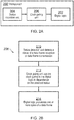
- Fig. 2A shows an illustrative embodiment of a transponder 200.
- the transponder 200 comprises digital logic 202, a status detection unit 204, and a clock gating unit 206.
- the digital logic 202 is configured to process one or more bytes of a data frame.
- the status detection unit 204 is configured to detect a status of a data frame reception or data frame transmission.
- the clock gating unit 206 is configured to apply clock gating to the digital logic 202 in dependence on the status of the data frame reception or in dependence on the status of the data frame transmission.
- Clock gating refers to stalling the clock to the digital logic and/or to preventing the system clock signal from reaching the digital logic.
- Fig. 2B shows an illustrative embodiment of a method 208 of operating a transponder.
- the method 208 comprises, at 210, that the status detection unit 204 detects a status of a data frame reception or data frame transmission, at 212, that the clock gating unit 206 applies clock gating to the digital logic 202 in dependence on the detected status, and at 214, that the digital logic 202 processes one or more bytes of a data frame.
- detecting the status of data frame reception comprises detecting an end of a Miller pause, and the clock gating unit is configured to apply said clock gating after said Miller pause.
- a transponder is set to reception status to receive one or more bytes of a data frame (a command from the reader), because it cannot transmit without a command from a reader.
- An analog demodulator detects Miller pauses and converts the Miller pauses to digital signals, which are used for detecting logic bits 0's and 1's. A transition of such a digital signal from high to low can be regarded as the end of a Miller pause. The same digital signal may be used to gate the digital logic, because the transponder has low power or no power during Miller pause.
- the clock gating unit is configured to apply clock gating after the Miller pause.
- the digital logic is generally active to copy the byte(s) from a receive buffer to internal memory or to execute any other operations.
- the clock gating By applying the clock gating, the power consumed by the digital logic is effectively controlled. In this way, the likelihood of a significant variation in voltage after a Miller pause may be reduced, which in turn reduces the risk that such a voltage variation is detected as a wrong Miller pause by the demodulator. Furthermore, the likelihood of a significant voltage drop at the start of the next Miller pause may also be reduced, so that the minimum operating field strength does not increase to an unacceptable level.
- detecting the status of data frame transmission comprises detecting that the digital logic is active during the transmission of a response, wherein the clock gating unit is configured to apply said clock gating while the digital logic is active.
- detecting that the digital logic is active comprises detecting that the digital logic is copying response data to a transmission buffer.
- a transponder performs, once a command is received, its specific operations and prepares response data for transmission by setting the transponder status to transmission.
- the response data may for example comprise response bytes.
- a CPU subsystem is generally active to copy response data byte(s), one after the other, from internal memory to the transmit buffer or to execute any other operations.
- the clock gating unit is configured to apply clock gating while the digital logic is active during the transmission of a response. In this way, the likelihood that power drops occur during response transmissions may be reduced, which in turn reduces the risk of errors in the response detection by the reader.
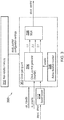
- Fig. 3 shows an illustrative embodiment of a clock gating subsystem 300 of a transponder.
- the clock gating subsystem 300 comprises a clock gating unit 302, a non-volatile memory 310, and a synchronizer 312.
- the clock gating unit 302 comprises a clock_control generator 304, a multiplexer 306, and an active duration counter 308.
- a transponder's demodulator may be sensitive to the drop or rise of the voltage between the Miller pauses of a command.
- a capacitor is often used as a secondary power source, in addition to the power harvested from the field, which may cause the drop or rise of the voltage.
- the drop or rise in the voltage may be regulated by gating the digital logic clocks with a predefined clock during reception.
- the clock control may be optimized so as to regulate the voltage between Miller pauses and to ensure a safe capture of the command by providing a sufficient number of active clocks to perform a copy operation or to perform other digital operations.
- the voltage regulator logic may be configured via the non-volatile memory 310. The use of the non-volatile memory 310 results in effective and practical implementation of the clock gating mechanism.
- the clock control generator 304 may retrieve clock control configuration settings (i.e. parameters) from said non-volatile memory 310.
- the active duration of the clock control may also be a configuration setting or parameter stored in the non-volatile memory 310.
- the active duration may be defined as the number of clock cycles during which the configured gated clock control is active from the end of a Miller pause. After the active duration, the clock to the digital logic is gated until the next Miller pause.
- the synchronizer 312 is configured to synchronize an asynchronous demodulated signal with the digital logic clock domain.
- the clock control generator 304 is configured to generate different clock control signals, in dependence on the configuration settings.
- the configuration settings or parameters may be as follows:
- a 2-bit counter may be used to generate these signals. This module may be enabled during command reception ( rx _ enable ).
- the active duration counter 308 may be a 5-bit counter, which is used to enable the clock control generator 304 for a configured active duration cycle count (e.g. stored as parameter act _ duration in the non-volatile memory 310). If the parameter act _ duration is set to 0, then this is treated as a disablement of the active duration feature.
- the multiplexer 306 is configured to multiplex the three types of clock-gating signals based on the configuration settings.
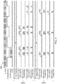
- Fig. 4 shows an illustrative embodiment of the use 400 of different programmable parameters.
- the active duration may be a programmable parameter ( act _ duration ) stored in the non-volatile memory 310.
- the parameter act _ duration has the value 00: this means that the feature to limit the number of active duration clocks after the Miller pause ( dmod ) has been disabled. In other words, it means that the configured clock gating is applied until the next Miller pause.
- the parameter act _ duration has the value 04: this means that the feature to limit the number of active duration clocks after the Miller pause ( dmod ) has been enabled and has been set to four.
- the configured clock gating is applied during four cycles after the end of Miller pause, and subsequently the clock is gated until the next Miller pause.
- the clock gating unit 304 is further configured to apply a configured clock gating for a predefined maximum number of clock cycles.
- the configured clock gating comprises disabling the digital logic during a first predefined number of clock cycles and enabling the digital logic during a second predefined number of clock cycles.
- the first predefined number and the second predefined number may for example be 1 and 1, 2 and 2, respectively 3 and 1, as described above.
- the second problem shown in Fig. 1B may be avoided.
- the active duration is disabled, there might be active clocks until the next Miller pause, which might result in a voltage drop at the start of next Miller pause.
- the active clocks encroach the next Miller pause.
- the voltage may be fully recovered before the next Miller pause.
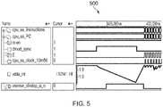
- Fig. 5 shows a simulation result 500 with applied clock gating.
- Fig. 5 shows a simulation waveform for a command that is being received by a transponder ( dmod _ sync ).
- the clock-control (E) starts and the digital processing is stalled for predefined intervals to regulate the power or voltage ( vdda _ int ).
- the variation in voltage ( vdda _ int ) between Miller pauses is well regulated (not dropping below 1.8V) and also the digital processing is completed ahead of the next Miller pause.
- the starting voltage ( vdda _ int ) at the start of the next Miller pause is at full strength as the digital processing is completed before the next Miller pause. This may result in a lower minimum operating field strength (H min ) as it may avoid triggering a low voltage reset.
- the systems and methods described herein may at least partially be embodied by a computer program or a plurality of computer programs, which may exist in a variety of forms both active and inactive in a single computer system or across multiple computer systems.
- they may exist as software program(s) comprised of program instructions in source code, object code, executable code or other formats for performing some of the steps.
- Any of the above may be embodied on a computer-readable medium, which may include storage devices and signals, in compressed or uncompressed form.
- the term "computer” refers to any electronic device comprising a processor, such as a general-purpose central processing unit (CPU), a specific-purpose processor or a microcontroller.
- a computer is capable of receiving data (an input), of performing a sequence of predetermined operations thereupon, and of producing thereby a result in the form of information or signals (an output).
- the term "computer” will mean either a processor in particular or more generally a processor in association with an assemblage of interrelated elements contained within a single case or housing.
- processor or “processing unit” refers to a data processing circuit that may be a microprocessor, a co-processor, a microcontroller, a microcomputer, a central processing unit, a field programmable gate array (FPGA), a programmable logic circuit, and/or any circuit that manipulates signals (analog or digital) based on operational instructions that are stored in a memory.
- memory refers to a storage circuit or multiple storage circuits such as read-only memory, random access memory, volatile memory, non-volatile memory, static memory, dynamic memory, Flash memory, cache memory, and/or any circuit that stores digital information.
- a "computer-readable medium” or “storage medium” may be any means that can contain, store, communicate, propagate, or transport a computer program for use by or in connection with the instruction execution system, apparatus, or device.
- the computer-readable medium may be, for example but not limited to, an electronic, magnetic, optical, electromagnetic, infrared, or semiconductor system, apparatus, device, or propagation medium.
- the computer-readable medium may include the following: an electrical connection having one or more wires, a portable computer diskette, a random access memory (RAM), a read-only memory (ROM), an erasable programmable read-only memory (EPROM or Flash memory), an optical fiber, a portable compact disc read-only memory (CDROM), a digital versatile disc (DVD), a Blu-ray disc (BD), and a memory card.
- RAM random access memory
- ROM read-only memory
- EPROM or Flash memory erasable programmable read-only memory
- CDROM compact disc read-only memory
- DVD digital versatile disc
- BD Blu-ray disc
Landscapes
- Engineering & Computer Science (AREA)
- Theoretical Computer Science (AREA)
- Physics & Mathematics (AREA)
- General Physics & Mathematics (AREA)
- General Engineering & Computer Science (AREA)
- Computer Networks & Wireless Communication (AREA)
- Computer Hardware Design (AREA)
- Microelectronics & Electronic Packaging (AREA)
- Artificial Intelligence (AREA)
- Computer Vision & Pattern Recognition (AREA)
- Near-Field Transmission Systems (AREA)
Abstract
Description
- The present disclosure relates to a transponder. Furthermore, the present disclosure relates to a method of operating a transponder, and to a corresponding computer program. A transponder, such as a radio frequency identification (RFID) transponder, may receive commands from a reader and respond to those commands. However, the communication between the transponder and the reader may be susceptible to problems. For example, some commands may not be properly received or processed by the transponder. Similarly, some responses may not be properly received or processed by the reader.
- In accordance with a first aspect of the present disclosure, a transponder is provided, comprising: digital logic for processing one or more portions of a data frame; a status detection unit configured to detect a status of a data frame reception or data frame transmission; a clock gating unit configured to apply clock gating to said digital logic in dependence on the status of said data frame reception or data frame transmission.
- In an embodiment, detecting the status of data frame reception comprises detecting an end of a Miller pause, and the clock gating unit is configured to apply said clock gating after said Miller pause.
- In an embodiment, detecting the status of data frame transmission comprises detecting that the digital logic is active during the transmission of a response, and the clock gating unit is configured to apply said clock gating while the digital logic is active.
- In an embodiment, detecting that the digital logic is active comprises detecting that the digital logic is copying response data to a transmission buffer.
- In an embodiment, applying the clock gating comprises disabling the digital logic during a first predefined number of clock cycles and enabling the digital logic during a second predefined number of clock cycles.
- In an embodiment, the first predefined number is one and the second predefined number is one; the first predefined number is two and the second predefined number is two; or the first predefined number is three and the second predefined number is one.
- In an embodiment, disabling the digital logic and enabling the digital logic are repeated.
- In an embodiment, the clock gating unit is further configured to apply said disabling and enabling for a predefined maximum number of clock cycles.
- In an embodiment, the first predefined number of clock cycles, the second predefined number of clock cycles, and/or the predefined maximum number of clock cycles are programmable parameters.
- In an embodiment, the transponder further comprises a memory for storing said programmable parameters.
- In an embodiment, said memory is a non-volatile memory.
- In an embodiment, the transponder is a radio frequency identification (RFID) transponder, in particular an RFID tag or an RFID card.
- In accordance with a second aspect of the present disclosure, a method of operating a transponder is conceived, the method comprising: detecting, by a status detection unit of said transponder, a status of a data frame reception or data frame transmission; applying, by a clock gating unit of said transponder, clock gating to digital logic of said transponder in dependence on the status of said data frame reception or data frame transmission; processing, by said digital logic, one or more portions of a data frame.
- In accordance with the third aspect of the present disclosure, a computer program is provided, comprising instructions that, when executed by a processing unit, carry out a method of the kind set forth.
- In an embodiment, a non-transitory computer-readable medium comprising a computer program of the kind set forth.
- Embodiments will be described in more detail with reference to the appended drawings, in which:
-
Fig. 1A shows an example of an operation of a transponder; -
Fig. 1B shows an example of a command frame reception of a transponder; -
Fig. 2A shows an illustrative embodiment of a transponder; -
Fig. 2B shows an illustrative embodiment of a method of operating a transponder; -
Fig. 3 shows an illustrative embodiment of a clock gating subsystem of a transponder; -
Fig. 4 shows an illustrative embodiment of the use of different programmable parameters; -
Fig. 5 shows a simulation result with applied clock gating. - Nowadays, RFID transponders are widely used, in different areas of industry and commerce and for various purposes. RFID transponders may for example be embodied as so-called RFID tags or RFID cards. It is noted that, in the present disclosure, near field communication (NFC) transponders are regarded as a specific type of RFID transponders. Thus, the principles described herein may also be applied to NFC transponders. As mentioned above, a transponder, such as a radio frequency identification (RFID) transponder, may receive commands from a reader and respond to those commands. However, the communication between the transponder and the reader may be susceptible to problems. For example, some commands may not be properly received or processed by the transponder. Similarly, some responses may not be properly received or processed by the reader.
-
Fig. 1A shows an example of anoperation 100 of a transponder. During communication with a reader, once a command is received by the transponder, it should be decoded, processed and a response should be transmitted back to the reader. During command reception there is often a drop of the voltage due to active digital logic which captures or processes a received command. A voltage sensor based mechanism can be used to gate clocks of most of the active digital logic momentarily to reduce power consumption and resume on voltage recovery. This is useful to avoid resets due to low voltage, particularly at lower field strengths. This is referred to as a clock-stop concept. The clock-stop concept or clock-stop feature enables achieving a higher distance of operation of the transponder from the reader (i.e. a lower minimal field strength Hmin). - The waveform shown in
Fig. 1 illustrates that a clock-stop is triggered (vsens_clkstop_a_o) each time that the voltage drops below 1.8V (vdda_int). Thus, the digital logic clocks should be gated using vsens_clkstop_a_o. It is noted that vdda_int denotes an internal signal that represents the operating voltage of the transponder. -
Fig. 1B shows another example of anoperation 102 of a transponder. According to the technical standard ISO/IEC14443-2, section "Communication signal interface Type A", a reader communicates to a transponder a specific sequence oflogical bits 0/1, which are amplitude modulated by the reader. This amplitude modulation of a created radio frequency (RF) field is referred to as a Miller pause in said technical standard ISO/IEC14443-2. During the Miller pause a transponder has low or no power. While receiving a command from a reader, to operate at lower field strength, most of the digital logic clock of an RFID transponder is gated during a demodulator Miller pause. However, the transponder's digital logic (CPU subsystem) remains ungated after the Miller pause, in order to store (i.e. process) one or more bytes of the received command frame in a transponder memory. Unfortunately, such an ungated CPU subsystem clock results in a higher digital power consumption, and the demodulator of the tag may detect such a drop of voltage as a Miller pause. This, in turn, may result in a wrong Miller decoding and not responding to the command. This may predominantly be visible for higher baud rates such as 212 kbps, 424 kbps and 848 kbps, due to a lower demodulator sensitivity to detect lower Miller pause depths (for example modulation depths of 40%). -
Fig. 1B shows a simulation waveform with a command being received by the transponder (dmod_sync). After the Miller pause (dmod_sync) the digital processing starts and consumes power causing a voltage drop (vdda_int). A traditional voltage sensor based clock-stop (vsens_clkstop_a_o) is triggered after reaching a threshold voltage (1.8V). This clock-stop (vsens_clkstop_a_o) gates the digital processing until the voltage is recovered (vdda_int). A first problem is that the variation in voltage (vdda_int) between Miller pauses may be detected by the demodulator of the transponder as a wrong Miller pause. A second problem is that the starting voltage (vdda_int) at the start of the next Miller pause may drop due to the digital processing until the start of the next Miller pause; this may result in a higher minimum operating field strength (Hmin) as it can trigger a low voltage reset (for example a 1.2V reset in the present example). - Similarly, another problem (not shown) may occur while a transponder transmits a response back to the reader. In particular, while transmitting said response, the transponder's digital logic copies response bytes to a transmit buffer of said transponder. Since this copying may involve an activity of the central processing unit (CPU), power drops may occur, which may become visible as noise to the reader during response detection. Generally speaking, any activity of the CPU may become visible as noise to the reader during response detection. Readers often employ a signal-to-noise ratio (SNR), and the noise generated as a result of systematic processing by the CPU may be significantly visible. This, in turn, may result in errors in the response detection by the reader, depending on the reader's response detection sensitivity.
- Now a transponder and a corresponding method of operating a transponder will be discussed, which may alleviate at least some of the aforementioned problems.
- In accordance with the present disclosure, a transponder is provided, comprising digital logic for processing one or more portions of a data frame, a status detection unit configured to detect a status of a data frame reception or data frame transmission, and a clock gating unit configured to apply clock gating to said digital logic in dependence on the status of said data frame reception or data frame transmission. By detecting the status of a data frame reception or data frame transmission, and applying clock gating to the digital logic in dependence on the detected status, the activity of the digital logic can effectively be controlled or tuned in dependence on the status of data frame reception or transmission. Thereby, voltage variations caused by the digital processing of a received data frame (e.g. a command frame) or a data frame that is being prepared for transmission or being transmitted (e.g. a response frame) can be avoided or at least significantly reduced. In this way, at least some of the above-mentioned errors can be avoided. It is noted that said portions of the data frame may be bytes of the data frame. However, other portions of the data frame may also be processed by the digital logic, and the presently disclosed status-dependent clock gating may be applied equally well to digital logic that processes other portions than bytes (e.g., portions comprising any number of bits).
-
Fig. 2A shows an illustrative embodiment of atransponder 200. Thetransponder 200 comprisesdigital logic 202, a status detection unit 204, and aclock gating unit 206. Thedigital logic 202 is configured to process one or more bytes of a data frame. Furthermore, the status detection unit 204 is configured to detect a status of a data frame reception or data frame transmission. Finally, theclock gating unit 206 is configured to apply clock gating to thedigital logic 202 in dependence on the status of the data frame reception or in dependence on the status of the data frame transmission. Clock gating refers to stalling the clock to the digital logic and/or to preventing the system clock signal from reaching the digital logic. -
Fig. 2B shows an illustrative embodiment of amethod 208 of operating a transponder. Themethod 208 comprises, at 210, that the status detection unit 204 detects a status of a data frame reception or data frame transmission, at 212, that theclock gating unit 206 applies clock gating to thedigital logic 202 in dependence on the detected status, and at 214, that thedigital logic 202 processes one or more bytes of a data frame. - In an embodiment, detecting the status of data frame reception comprises detecting an end of a Miller pause, and the clock gating unit is configured to apply said clock gating after said Miller pause. By default, a transponder is set to reception status to receive one or more bytes of a data frame (a command from the reader), because it cannot transmit without a command from a reader. An analog demodulator detects Miller pauses and converts the Miller pauses to digital signals, which are used for detecting
logic bits 0's and 1's. A transition of such a digital signal from high to low can be regarded as the end of a Miller pause. The same digital signal may be used to gate the digital logic, because the transponder has low power or no power during Miller pause. The clock gating unit is configured to apply clock gating after the Miller pause. The digital logic is generally active to copy the byte(s) from a receive buffer to internal memory or to execute any other operations. By applying the clock gating, the power consumed by the digital logic is effectively controlled. In this way, the likelihood of a significant variation in voltage after a Miller pause may be reduced, which in turn reduces the risk that such a voltage variation is detected as a wrong Miller pause by the demodulator. Furthermore, the likelihood of a significant voltage drop at the start of the next Miller pause may also be reduced, so that the minimum operating field strength does not increase to an unacceptable level. - In an embodiment, detecting the status of data frame transmission comprises detecting that the digital logic is active during the transmission of a response, wherein the clock gating unit is configured to apply said clock gating while the digital logic is active. Furthermore, in a practical and effective implementation, detecting that the digital logic is active comprises detecting that the digital logic is copying response data to a transmission buffer. A transponder performs, once a command is received, its specific operations and prepares response data for transmission by setting the transponder status to transmission. The response data may for example comprise response bytes. During transmission a CPU subsystem is generally active to copy response data byte(s), one after the other, from internal memory to the transmit buffer or to execute any other operations. The clock gating unit is configured to apply clock gating while the digital logic is active during the transmission of a response. In this way, the likelihood that power drops occur during response transmissions may be reduced, which in turn reduces the risk of errors in the response detection by the reader.
-
Fig. 3 shows an illustrative embodiment of aclock gating subsystem 300 of a transponder. Theclock gating subsystem 300 comprises aclock gating unit 302, anon-volatile memory 310, and asynchronizer 312. Theclock gating unit 302 comprises aclock_control generator 304, amultiplexer 306, and anactive duration counter 308. As mentioned above, a transponder's demodulator may be sensitive to the drop or rise of the voltage between the Miller pauses of a command. A capacitor is often used as a secondary power source, in addition to the power harvested from the field, which may cause the drop or rise of the voltage. In accordance with the present disclosure, the drop or rise in the voltage may be regulated by gating the digital logic clocks with a predefined clock during reception. The clock control may be optimized so as to regulate the voltage between Miller pauses and to ensure a safe capture of the command by providing a sufficient number of active clocks to perform a copy operation or to perform other digital operations. The voltage regulator logic may be configured via thenon-volatile memory 310. The use of thenon-volatile memory 310 results in effective and practical implementation of the clock gating mechanism. In particular, theclock control generator 304 may retrieve clock control configuration settings (i.e. parameters) from saidnon-volatile memory 310. The choice of a high regulation (3:1) or medium regulation (2:2 or 1:1) can also be configured using thenon-volatile memory 310. In addition, the active duration of the clock control may also be a configuration setting or parameter stored in thenon-volatile memory 310. The active duration may be defined as the number of clock cycles during which the configured gated clock control is active from the end of a Miller pause. After the active duration, the clock to the digital logic is gated until the next Miller pause. Thesynchronizer 312 is configured to synchronize an asynchronous demodulated signal with the digital logic clock domain. Theclock control generator 304 is configured to generate different clock control signals, in dependence on the configuration settings. The configuration settings or parameters may be as follows: - 1:1 → The digital logic (CPU subsystem) is disabled during one cycle of a 13.56 MHz clock and enabled during the next one cycle. This is repeated.
- 2:2 → The digital logic (CPU subsystem) is disabled during two cycles of a 13.56 MHz clock and enabled during the next two cycles. This is repeated.
- 3:1 → The digital logic (CPU subsystem) is disabled during three cycles of a 13.56 MHz clock and enabled during the next one cycle. This is repeated.
- These values further enable an effective and practical implementation of the clock gating mechanism. A 2-bit counter may be used to generate these signals. This module may be enabled during command reception (rx_enable). The
active duration counter 308 may be a 5-bit counter, which is used to enable theclock control generator 304 for a configured active duration cycle count (e.g. stored as parameter act_duration in the non-volatile memory 310). If the parameter act_duration is set to 0, then this is treated as a disablement of the active duration feature. Themultiplexer 306 is configured to multiplex the three types of clock-gating signals based on the configuration settings. -
Fig. 4 shows an illustrative embodiment of theuse 400 of different programmable parameters. In particular, two examples are shown, in order to illustrate the use of the active duration feature. As mentioned above, the active duration may be a programmable parameter (act_duration) stored in thenon-volatile memory 310. In a first case, the parameter act_duration has the value 00: this means that the feature to limit the number of active duration clocks after the Miller pause (dmod) has been disabled. In other words, it means that the configured clock gating is applied until the next Miller pause. In a second case, the parameter act_duration has the value 04: this means that the feature to limit the number of active duration clocks after the Miller pause (dmod) has been enabled and has been set to four. In other words, the configured clock gating is applied during four cycles after the end of Miller pause, and subsequently the clock is gated until the next Miller pause. Thus, in an embodiment, theclock gating unit 304 is further configured to apply a configured clock gating for a predefined maximum number of clock cycles. The configured clock gating comprises disabling the digital logic during a first predefined number of clock cycles and enabling the digital logic during a second predefined number of clock cycles. The first predefined number and the second predefined number may for example be 1 and 1, 2 and 2, respectively 3 and 1, as described above. In this way, the second problem shown inFig. 1B may be avoided. In particular, in case the active duration is disabled, there might be active clocks until the next Miller pause, which might result in a voltage drop at the start of next Miller pause. Using the active duration, it is avoided that the active clocks encroach the next Miller pause. As a result, the voltage may be fully recovered before the next Miller pause. -
Fig. 5 shows asimulation result 500 with applied clock gating. In particular,Fig. 5 shows a simulation waveform for a command that is being received by a transponder (dmod_sync). After the Miller pause (dmod_sync) the clock-control (E) starts and the digital processing is stalled for predefined intervals to regulate the power or voltage (vdda_int). The variation in voltage (vdda_int) between Miller pauses is well regulated (not dropping below 1.8V) and also the digital processing is completed ahead of the next Miller pause. It can also be observed that the starting voltage (vdda_int) at the start of the next Miller pause is at full strength as the digital processing is completed before the next Miller pause. This may result in a lower minimum operating field strength (Hmin) as it may avoid triggering a low voltage reset. - The systems and methods described herein may at least partially be embodied by a computer program or a plurality of computer programs, which may exist in a variety of forms both active and inactive in a single computer system or across multiple computer systems. For example, they may exist as software program(s) comprised of program instructions in source code, object code, executable code or other formats for performing some of the steps. Any of the above may be embodied on a computer-readable medium, which may include storage devices and signals, in compressed or uncompressed form.
- As used herein, the term "computer" refers to any electronic device comprising a processor, such as a general-purpose central processing unit (CPU), a specific-purpose processor or a microcontroller. A computer is capable of receiving data (an input), of performing a sequence of predetermined operations thereupon, and of producing thereby a result in the form of information or signals (an output). Depending on the context, the term "computer" will mean either a processor in particular or more generally a processor in association with an assemblage of interrelated elements contained within a single case or housing.
- The term "processor" or "processing unit" refers to a data processing circuit that may be a microprocessor, a co-processor, a microcontroller, a microcomputer, a central processing unit, a field programmable gate array (FPGA), a programmable logic circuit, and/or any circuit that manipulates signals (analog or digital) based on operational instructions that are stored in a memory. The term "memory" refers to a storage circuit or multiple storage circuits such as read-only memory, random access memory, volatile memory, non-volatile memory, static memory, dynamic memory, Flash memory, cache memory, and/or any circuit that stores digital information.
- As used herein, a "computer-readable medium" or "storage medium" may be any means that can contain, store, communicate, propagate, or transport a computer program for use by or in connection with the instruction execution system, apparatus, or device. The computer-readable medium may be, for example but not limited to, an electronic, magnetic, optical, electromagnetic, infrared, or semiconductor system, apparatus, device, or propagation medium. More specific examples (non-exhaustive list) of the computer-readable medium may include the following: an electrical connection having one or more wires, a portable computer diskette, a random access memory (RAM), a read-only memory (ROM), an erasable programmable read-only memory (EPROM or Flash memory), an optical fiber, a portable compact disc read-only memory (CDROM), a digital versatile disc (DVD), a Blu-ray disc (BD), and a memory card.
- It is noted that the embodiments above have been described with reference to different subject-matters. In particular, some embodiments may have been described with reference to method-type claims whereas other embodiments may have been described with reference to apparatus-type claims. However, a person skilled in the art will gather from the above that, unless otherwise indicated, in addition to any combination of features belonging to one type of subject-matter also any combination of features relating to different subject-matters, in particular a combination of features of the method-type claims and features of the apparatus-type claims, is considered to be disclosed with this document.
- Furthermore, it is noted that the drawings are schematic. In different drawings, similar or identical elements are provided with the same reference signs. Furthermore, it is noted that in an effort to provide a concise description of the illustrative embodiments, implementation details which fall into the customary practice of the skilled person may not have been described. It should be appreciated that in the development of any such implementation, as in any engineering or design project, numerous implementation-specific decisions must be made in order to achieve the developers' specific goals, such as compliance with system-related and business-related constraints, which may vary from one implementation to another. Moreover, it should be appreciated that such a development effort might be complex and time consuming, but would nevertheless be a routine undertaking of design, fabrication, and manufacture for those of ordinary skill.
- Finally, it is noted that the skilled person will be able to design many alternative embodiments without departing from the scope of the appended claims. In the claims, any reference sign placed between parentheses shall not be construed as limiting the claim. The word "comprise(s)" or "comprising" does not exclude the presence of elements or steps other than those listed in a claim. The word "a" or "an" preceding an element does not exclude the presence of a plurality of such elements. Measures recited in the claims may be implemented by means of hardware comprising several distinct elements and/or by means of a suitably programmed processor. In a device claim enumerating several means, several of these means may be embodied by one and the same item of hardware. The mere fact that certain measures are recited in mutually different dependent claims does not indicate that a combination of these measures cannot be used to advantage.
-
- 100
- operation of a transponder
- 102
- operation of a transponder
- 200
- transponder
- 202
- digital logic
- 204
- status detection unit
- 206
- clock gating unit
- 208
- method of operating a transponder
- 210
- status detection unit detects a status of a data frame receipt or data frame transmission
- 212
- clock gating unit applies clock gating to the digital logic in dependence on the detected status
- 214
- digital logic processes one or more data frames
- 300
- clock gating subsystem of transponder
- 302
- clock gating unit
- 304
- clock_control generator (counter)
- 306
- multiplexer
- 308
- active duration counter
- 310
- non-volatile memory
- 312
- synchronizer
- 400
- use of different programmable parameters
- 500
- simulation result with applied clock gating
Claims (15)
- A transponder, comprising:digital logic for processing one or more portions of a data frame;a status detection unit configured to detect a status of a data frame reception or data frame transmission;a clock gating unit configured to apply clock gating to said digital logic in dependence on the status of said data frame reception or data frame transmission.
- The transponder of claim 1, wherein detecting the status of data frame reception comprises detecting an end of a Miller pause, and wherein the clock gating unit is configured to apply said clock gating after said Miller pause.
- The transponder of any preceding claim, wherein detecting the status of data frame transmission comprises detecting that the digital logic is active during the transmission of a response, and wherein the clock gating unit is configured to apply said clock gating while the digital logic is active.
- The transponder of claim 3, wherein detecting that the digital logic is active comprises detecting that the digital logic is copying response data to a transmission buffer.
- The transponder of any preceding claim, wherein applying the clock gating comprises disabling the digital logic during a first predefined number of clock cycles and enabling the digital logic during a second predefined number of clock cycles.
- The transponder of claim 5, wherein:the first predefined number is one and the second predefined number is one;the first predefined number is two and the second predefined number is two; orthe first predefined number is three and the second predefined number is one.
- The transponder of claim 5 or 6, wherein disabling the digital logic and enabling the digital logic are repeated.
- The transponder of any one of claims 5 to 7, wherein the clock gating unit is further configured to apply said disabling and enabling for a predefined maximum number of clock cycles.
- The transponder of any one of claims 5 to 8, wherein the first predefined number of clock cycles, the second predefined number of clock cycles, and/or the predefined maximum number of clock cycles are programmable parameters.
- The transponder of claim 9, further comprising a memory for storing said programmable parameters.
- The transponder of claim 10, wherein said memory is a non-volatile memory.
- The transponder of any preceding claim, being a radio frequency identification, RFID, transponder, in particular an RFID tag or an RFID card.
- A method of operating a transponder, the method comprising:detecting, by a status detection unit of said transponder, a status of a data frame reception or data frame transmission;applying, by a clock gating unit of said transponder, clock gating to digital logic of said transponder in dependence on the status of said data frame reception or data frame transmission;processing, by said digital logic, one or more portions of a data frame.
- A computer program comprising instructions that, when executed by a processing unit, carry out the method of claim 13.
- A non-transitory computer-readable medium comprising the computer program of claim 14.
Priority Applications (2)
| Application Number | Priority Date | Filing Date | Title |
|---|---|---|---|
| EP18173666.1A EP3572968B1 (en) | 2018-05-22 | 2018-05-22 | Clock gating unit for a transponder |
| US16/406,083 US11068040B2 (en) | 2018-05-22 | 2019-05-08 | Clock gating unit for a transponder |
Applications Claiming Priority (1)
| Application Number | Priority Date | Filing Date | Title |
|---|---|---|---|
| EP18173666.1A EP3572968B1 (en) | 2018-05-22 | 2018-05-22 | Clock gating unit for a transponder |
Publications (2)
| Publication Number | Publication Date |
|---|---|
| EP3572968A1 true EP3572968A1 (en) | 2019-11-27 |
| EP3572968B1 EP3572968B1 (en) | 2021-08-04 |
Family
ID=62244305
Family Applications (1)
| Application Number | Title | Priority Date | Filing Date |
|---|---|---|---|
| EP18173666.1A Active EP3572968B1 (en) | 2018-05-22 | 2018-05-22 | Clock gating unit for a transponder |
Country Status (2)
| Country | Link |
|---|---|
| US (1) | US11068040B2 (en) |
| EP (1) | EP3572968B1 (en) |
Families Citing this family (1)
| Publication number | Priority date | Publication date | Assignee | Title |
|---|---|---|---|---|
| US11209891B2 (en) * | 2019-11-27 | 2021-12-28 | Robert Bosch Gmbh | Clock control to increase robustness of a serial bus interface |
Citations (7)
| Publication number | Priority date | Publication date | Assignee | Title |
|---|---|---|---|---|
| US20060109087A1 (en) * | 2004-11-24 | 2006-05-25 | Electronics And Telecommunications Research Institute | Low power digital circuit for RFID tag |
| US20070297214A1 (en) * | 2006-06-09 | 2007-12-27 | Semiconductor Energy Laboratory Co., Ltd. | Semiconductor device |
| US20080266061A1 (en) * | 2007-04-26 | 2008-10-30 | Em Microelectronic-Marin Sa | Transponder circuit with double clock extractor unit |
| US20150054571A1 (en) * | 2013-08-21 | 2015-02-26 | Semiconductor Energy Laboratory Co., Ltd. | Charge pump circuit and semiconductor device including the same |
| CN104636691A (en) * | 2013-11-13 | 2015-05-20 | 成都新方洲信息技术有限公司 | Transponder for RFID (radio frequency identification) system |
| US20150254543A1 (en) * | 2010-10-05 | 2015-09-10 | Nxp B.V. | Smart card |
| US20150347791A1 (en) * | 2013-02-07 | 2015-12-03 | Newport Digital Technologies Australia Pty Ltd | Rfid tracking |
Family Cites Families (9)
| Publication number | Priority date | Publication date | Assignee | Title |
|---|---|---|---|---|
| US5504485A (en) | 1994-07-21 | 1996-04-02 | Amtech Corporation | System for preventing reading of undesired RF signals |
| DE19732643A1 (en) * | 1997-07-29 | 1999-02-04 | Siemens Ag | Circuit arrangement for tamper-proof reception of an OOK-modulated signal |
| WO1999050738A2 (en) * | 1998-03-27 | 1999-10-07 | Koninklijke Philips Electronics N.V. | Passive data carrier having means for reducing the power consumption |
| FR2812142A1 (en) * | 2000-07-21 | 2002-01-25 | Microcid Sa | PASSIVE TRANSPONDER AND READER FOR NON-CONTACT IDENTIFICATION OF SUCH TRANSPONDERS |
| US8193912B1 (en) | 2008-03-13 | 2012-06-05 | Impinj, Inc. | RFID tag dynamically adjusting clock frequency |
| US9064196B1 (en) | 2008-03-13 | 2015-06-23 | Impinj, Inc. | RFID tag dynamically adjusting clock frequency |
| US7605612B1 (en) * | 2008-05-16 | 2009-10-20 | International Business Machines Corporation | Techniques for reducing power requirements of an integrated circuit |
| KR101543646B1 (en) * | 2009-03-13 | 2015-08-12 | 삼성전자주식회사 | TYPE-A demodulator and integrated circuit card with it |
| US8076970B2 (en) * | 2009-06-10 | 2011-12-13 | Infineon Technologies Ag | Adaptive demodulator |
-
2018
- 2018-05-22 EP EP18173666.1A patent/EP3572968B1/en active Active
-
2019
- 2019-05-08 US US16/406,083 patent/US11068040B2/en active Active
Patent Citations (7)
| Publication number | Priority date | Publication date | Assignee | Title |
|---|---|---|---|---|
| US20060109087A1 (en) * | 2004-11-24 | 2006-05-25 | Electronics And Telecommunications Research Institute | Low power digital circuit for RFID tag |
| US20070297214A1 (en) * | 2006-06-09 | 2007-12-27 | Semiconductor Energy Laboratory Co., Ltd. | Semiconductor device |
| US20080266061A1 (en) * | 2007-04-26 | 2008-10-30 | Em Microelectronic-Marin Sa | Transponder circuit with double clock extractor unit |
| US20150254543A1 (en) * | 2010-10-05 | 2015-09-10 | Nxp B.V. | Smart card |
| US20150347791A1 (en) * | 2013-02-07 | 2015-12-03 | Newport Digital Technologies Australia Pty Ltd | Rfid tracking |
| US20150054571A1 (en) * | 2013-08-21 | 2015-02-26 | Semiconductor Energy Laboratory Co., Ltd. | Charge pump circuit and semiconductor device including the same |
| CN104636691A (en) * | 2013-11-13 | 2015-05-20 | 成都新方洲信息技术有限公司 | Transponder for RFID (radio frequency identification) system |
Non-Patent Citations (1)
| Title |
|---|
| "IDENTIFICATION CARDS etc", INTERNATIONAL STANDARD ISO/IEC, no. 14443-2, 1 July 2001 (2001-07-01), pages I - IV,01, XP001146901 * |
Also Published As
| Publication number | Publication date |
|---|---|
| EP3572968B1 (en) | 2021-08-04 |
| US11068040B2 (en) | 2021-07-20 |
| US20190361514A1 (en) | 2019-11-28 |
Similar Documents
| Publication | Publication Date | Title |
|---|---|---|
| EP3800767B1 (en) | Detection of nfc proximity ic cards (piccs) during wireless charging | |
| US9940489B2 (en) | Radiofrequency transponder circuit | |
| US11533081B2 (en) | NFC device detection | |
| KR20160015193A (en) | Improvements in rfid tracking | |
| EP3996425B1 (en) | Rf communication devices and operating methods | |
| US20220321173A1 (en) | Nfc device, operating method and computer program | |
| EP3457580B1 (en) | Nfc controller | |
| US7717349B2 (en) | Semiconductor device for IC tag, IC tag and control method for IC tag for detecting and executing command from radio wave | |
| JP2018151785A (en) | Transponder, interrogator, control method of transponder, control method of interrogator, information processing program, and recording medium | |
| US11068040B2 (en) | Clock gating unit for a transponder | |
| US7468668B2 (en) | Semiconductor device for IC tag, IC tag, and control method for IC tag for detecting and executing command from radio wave | |
| CN111914575B (en) | Transponder and method of operating the same | |
| TWI384402B (en) | Method of accessing rfid tag and circuit for determining whether to reply command sent from reader or not | |
| US11199621B2 (en) | Clock-stop frequency adjustment for a transponder | |
| CN112699694B (en) | Tag detection circuit of reader-writer and reader-writer | |
| US7429913B2 (en) | Low power digital circuit for RFID tag | |
| JP7654494B2 (en) | Tag Reader | |
| US11386192B2 (en) | Authentication token and method of operating the same | |
| JP3696796B2 (en) | Electromagnetic induction interrogation device and communication method | |
| CN117351691B (en) | Infrared control device, system, data transmission method, medium, and program product | |
| KR102152529B1 (en) | Method and apparatus for optical signal communication | |
| KR102391928B1 (en) | Apparatus and Method for Multi-Sensing, Door Lock System Using the Same | |
| JP2001307033A (en) | Non-contact ic card reader | |
| KR20040055983A (en) | Card reader and data processing method in card reader |
Legal Events
| Date | Code | Title | Description |
|---|---|---|---|
| PUAI | Public reference made under article 153(3) epc to a published international application that has entered the european phase |
Free format text: ORIGINAL CODE: 0009012 |
|
| STAA | Information on the status of an ep patent application or granted ep patent |
Free format text: STATUS: THE APPLICATION HAS BEEN PUBLISHED |
|
| AK | Designated contracting states |
Kind code of ref document: A1 Designated state(s): AL AT BE BG CH CY CZ DE DK EE ES FI FR GB GR HR HU IE IS IT LI LT LU LV MC MK MT NL NO PL PT RO RS SE SI SK SM TR |
|
| AX | Request for extension of the european patent |
Extension state: BA ME |
|
| STAA | Information on the status of an ep patent application or granted ep patent |
Free format text: STATUS: REQUEST FOR EXAMINATION WAS MADE |
|
| 17P | Request for examination filed |
Effective date: 20200527 |
|
| RBV | Designated contracting states (corrected) |
Designated state(s): AL AT BE BG CH CY CZ DE DK EE ES FI FR GB GR HR HU IE IS IT LI LT LU LV MC MK MT NL NO PL PT RO RS SE SI SK SM TR |
|
| STAA | Information on the status of an ep patent application or granted ep patent |
Free format text: STATUS: EXAMINATION IS IN PROGRESS |
|
| 17Q | First examination report despatched |
Effective date: 20200710 |
|
| GRAP | Despatch of communication of intention to grant a patent |
Free format text: ORIGINAL CODE: EPIDOSNIGR1 |
|
| STAA | Information on the status of an ep patent application or granted ep patent |
Free format text: STATUS: GRANT OF PATENT IS INTENDED |
|
| INTG | Intention to grant announced |
Effective date: 20210512 |
|
| GRAS | Grant fee paid |
Free format text: ORIGINAL CODE: EPIDOSNIGR3 |
|
| GRAA | (expected) grant |
Free format text: ORIGINAL CODE: 0009210 |
|
| STAA | Information on the status of an ep patent application or granted ep patent |
Free format text: STATUS: THE PATENT HAS BEEN GRANTED |
|
| AK | Designated contracting states |
Kind code of ref document: B1 Designated state(s): AL AT BE BG CH CY CZ DE DK EE ES FI FR GB GR HR HU IE IS IT LI LT LU LV MC MK MT NL NO PL PT RO RS SE SI SK SM TR |
|
| REG | Reference to a national code |
Ref country code: GB Ref legal event code: FG4D |
|
| REG | Reference to a national code |
Ref country code: AT Ref legal event code: REF Ref document number: 1417743 Country of ref document: AT Kind code of ref document: T Effective date: 20210815 |
|
| REG | Reference to a national code |
Ref country code: CH Ref legal event code: EP |
|
| REG | Reference to a national code |
Ref country code: DE Ref legal event code: R096 Ref document number: 602018021049 Country of ref document: DE |
|
| REG | Reference to a national code |
Ref country code: IE Ref legal event code: FG4D |
|
| REG | Reference to a national code |
Ref country code: LT Ref legal event code: MG9D |
|
| REG | Reference to a national code |
Ref country code: NL Ref legal event code: MP Effective date: 20210804 |
|
| REG | Reference to a national code |
Ref country code: AT Ref legal event code: MK05 Ref document number: 1417743 Country of ref document: AT Kind code of ref document: T Effective date: 20210804 |
|
| PG25 | Lapsed in a contracting state [announced via postgrant information from national office to epo] |
Ref country code: RS Free format text: LAPSE BECAUSE OF FAILURE TO SUBMIT A TRANSLATION OF THE DESCRIPTION OR TO PAY THE FEE WITHIN THE PRESCRIBED TIME-LIMIT Effective date: 20210804 Ref country code: SE Free format text: LAPSE BECAUSE OF FAILURE TO SUBMIT A TRANSLATION OF THE DESCRIPTION OR TO PAY THE FEE WITHIN THE PRESCRIBED TIME-LIMIT Effective date: 20210804 Ref country code: FI Free format text: LAPSE BECAUSE OF FAILURE TO SUBMIT A TRANSLATION OF THE DESCRIPTION OR TO PAY THE FEE WITHIN THE PRESCRIBED TIME-LIMIT Effective date: 20210804 Ref country code: ES Free format text: LAPSE BECAUSE OF FAILURE TO SUBMIT A TRANSLATION OF THE DESCRIPTION OR TO PAY THE FEE WITHIN THE PRESCRIBED TIME-LIMIT Effective date: 20210804 Ref country code: HR Free format text: LAPSE BECAUSE OF FAILURE TO SUBMIT A TRANSLATION OF THE DESCRIPTION OR TO PAY THE FEE WITHIN THE PRESCRIBED TIME-LIMIT Effective date: 20210804 Ref country code: NO Free format text: LAPSE BECAUSE OF FAILURE TO SUBMIT A TRANSLATION OF THE DESCRIPTION OR TO PAY THE FEE WITHIN THE PRESCRIBED TIME-LIMIT Effective date: 20211104 Ref country code: PT Free format text: LAPSE BECAUSE OF FAILURE TO SUBMIT A TRANSLATION OF THE DESCRIPTION OR TO PAY THE FEE WITHIN THE PRESCRIBED TIME-LIMIT Effective date: 20211206 Ref country code: AT Free format text: LAPSE BECAUSE OF FAILURE TO SUBMIT A TRANSLATION OF THE DESCRIPTION OR TO PAY THE FEE WITHIN THE PRESCRIBED TIME-LIMIT Effective date: 20210804 Ref country code: BG Free format text: LAPSE BECAUSE OF FAILURE TO SUBMIT A TRANSLATION OF THE DESCRIPTION OR TO PAY THE FEE WITHIN THE PRESCRIBED TIME-LIMIT Effective date: 20211104 Ref country code: LT Free format text: LAPSE BECAUSE OF FAILURE TO SUBMIT A TRANSLATION OF THE DESCRIPTION OR TO PAY THE FEE WITHIN THE PRESCRIBED TIME-LIMIT Effective date: 20210804 |
|
| PG25 | Lapsed in a contracting state [announced via postgrant information from national office to epo] |
Ref country code: PL Free format text: LAPSE BECAUSE OF FAILURE TO SUBMIT A TRANSLATION OF THE DESCRIPTION OR TO PAY THE FEE WITHIN THE PRESCRIBED TIME-LIMIT Effective date: 20210804 Ref country code: LV Free format text: LAPSE BECAUSE OF FAILURE TO SUBMIT A TRANSLATION OF THE DESCRIPTION OR TO PAY THE FEE WITHIN THE PRESCRIBED TIME-LIMIT Effective date: 20210804 Ref country code: GR Free format text: LAPSE BECAUSE OF FAILURE TO SUBMIT A TRANSLATION OF THE DESCRIPTION OR TO PAY THE FEE WITHIN THE PRESCRIBED TIME-LIMIT Effective date: 20211105 |
|
| PG25 | Lapsed in a contracting state [announced via postgrant information from national office to epo] |
Ref country code: NL Free format text: LAPSE BECAUSE OF FAILURE TO SUBMIT A TRANSLATION OF THE DESCRIPTION OR TO PAY THE FEE WITHIN THE PRESCRIBED TIME-LIMIT Effective date: 20210804 |
|
| PG25 | Lapsed in a contracting state [announced via postgrant information from national office to epo] |
Ref country code: DK Free format text: LAPSE BECAUSE OF FAILURE TO SUBMIT A TRANSLATION OF THE DESCRIPTION OR TO PAY THE FEE WITHIN THE PRESCRIBED TIME-LIMIT Effective date: 20210804 |
|
| REG | Reference to a national code |
Ref country code: DE Ref legal event code: R097 Ref document number: 602018021049 Country of ref document: DE |
|
| PG25 | Lapsed in a contracting state [announced via postgrant information from national office to epo] |
Ref country code: SM Free format text: LAPSE BECAUSE OF FAILURE TO SUBMIT A TRANSLATION OF THE DESCRIPTION OR TO PAY THE FEE WITHIN THE PRESCRIBED TIME-LIMIT Effective date: 20210804 Ref country code: SK Free format text: LAPSE BECAUSE OF FAILURE TO SUBMIT A TRANSLATION OF THE DESCRIPTION OR TO PAY THE FEE WITHIN THE PRESCRIBED TIME-LIMIT Effective date: 20210804 Ref country code: RO Free format text: LAPSE BECAUSE OF FAILURE TO SUBMIT A TRANSLATION OF THE DESCRIPTION OR TO PAY THE FEE WITHIN THE PRESCRIBED TIME-LIMIT Effective date: 20210804 Ref country code: EE Free format text: LAPSE BECAUSE OF FAILURE TO SUBMIT A TRANSLATION OF THE DESCRIPTION OR TO PAY THE FEE WITHIN THE PRESCRIBED TIME-LIMIT Effective date: 20210804 Ref country code: CZ Free format text: LAPSE BECAUSE OF FAILURE TO SUBMIT A TRANSLATION OF THE DESCRIPTION OR TO PAY THE FEE WITHIN THE PRESCRIBED TIME-LIMIT Effective date: 20210804 Ref country code: AL Free format text: LAPSE BECAUSE OF FAILURE TO SUBMIT A TRANSLATION OF THE DESCRIPTION OR TO PAY THE FEE WITHIN THE PRESCRIBED TIME-LIMIT Effective date: 20210804 |
|
| PLBE | No opposition filed within time limit |
Free format text: ORIGINAL CODE: 0009261 |
|
| STAA | Information on the status of an ep patent application or granted ep patent |
Free format text: STATUS: NO OPPOSITION FILED WITHIN TIME LIMIT |
|
| 26N | No opposition filed |
Effective date: 20220506 |
|
| PG25 | Lapsed in a contracting state [announced via postgrant information from national office to epo] |
Ref country code: IT Free format text: LAPSE BECAUSE OF FAILURE TO SUBMIT A TRANSLATION OF THE DESCRIPTION OR TO PAY THE FEE WITHIN THE PRESCRIBED TIME-LIMIT Effective date: 20210804 |
|
| PG25 | Lapsed in a contracting state [announced via postgrant information from national office to epo] |
Ref country code: SI Free format text: LAPSE BECAUSE OF FAILURE TO SUBMIT A TRANSLATION OF THE DESCRIPTION OR TO PAY THE FEE WITHIN THE PRESCRIBED TIME-LIMIT Effective date: 20210804 |
|
| REG | Reference to a national code |
Ref country code: CH Ref legal event code: PL |
|
| REG | Reference to a national code |
Ref country code: BE Ref legal event code: MM Effective date: 20220531 |
|
| GBPC | Gb: european patent ceased through non-payment of renewal fee |
Effective date: 20220522 |
|
| PG25 | Lapsed in a contracting state [announced via postgrant information from national office to epo] |
Ref country code: MC Free format text: LAPSE BECAUSE OF FAILURE TO SUBMIT A TRANSLATION OF THE DESCRIPTION OR TO PAY THE FEE WITHIN THE PRESCRIBED TIME-LIMIT Effective date: 20210804 Ref country code: LU Free format text: LAPSE BECAUSE OF NON-PAYMENT OF DUE FEES Effective date: 20220522 Ref country code: LI Free format text: LAPSE BECAUSE OF NON-PAYMENT OF DUE FEES Effective date: 20220531 Ref country code: CH Free format text: LAPSE BECAUSE OF NON-PAYMENT OF DUE FEES Effective date: 20220531 |
|
| PG25 | Lapsed in a contracting state [announced via postgrant information from national office to epo] |
Ref country code: IE Free format text: LAPSE BECAUSE OF NON-PAYMENT OF DUE FEES Effective date: 20220522 Ref country code: FR Free format text: LAPSE BECAUSE OF NON-PAYMENT OF DUE FEES Effective date: 20220531 |
|
| PG25 | Lapsed in a contracting state [announced via postgrant information from national office to epo] |
Ref country code: GB Free format text: LAPSE BECAUSE OF NON-PAYMENT OF DUE FEES Effective date: 20220522 Ref country code: BE Free format text: LAPSE BECAUSE OF NON-PAYMENT OF DUE FEES Effective date: 20220531 |
|
| P01 | Opt-out of the competence of the unified patent court (upc) registered |
Effective date: 20230725 |
|
| PG25 | Lapsed in a contracting state [announced via postgrant information from national office to epo] |
Ref country code: HU Free format text: LAPSE BECAUSE OF FAILURE TO SUBMIT A TRANSLATION OF THE DESCRIPTION OR TO PAY THE FEE WITHIN THE PRESCRIBED TIME-LIMIT; INVALID AB INITIO Effective date: 20180522 |
|
| PG25 | Lapsed in a contracting state [announced via postgrant information from national office to epo] |
Ref country code: MK Free format text: LAPSE BECAUSE OF FAILURE TO SUBMIT A TRANSLATION OF THE DESCRIPTION OR TO PAY THE FEE WITHIN THE PRESCRIBED TIME-LIMIT Effective date: 20210804 Ref country code: CY Free format text: LAPSE BECAUSE OF FAILURE TO SUBMIT A TRANSLATION OF THE DESCRIPTION OR TO PAY THE FEE WITHIN THE PRESCRIBED TIME-LIMIT Effective date: 20210804 |
|
| PG25 | Lapsed in a contracting state [announced via postgrant information from national office to epo] |
Ref country code: TR Free format text: LAPSE BECAUSE OF FAILURE TO SUBMIT A TRANSLATION OF THE DESCRIPTION OR TO PAY THE FEE WITHIN THE PRESCRIBED TIME-LIMIT Effective date: 20210804 |
|
| PG25 | Lapsed in a contracting state [announced via postgrant information from national office to epo] |
Ref country code: MT Free format text: LAPSE BECAUSE OF FAILURE TO SUBMIT A TRANSLATION OF THE DESCRIPTION OR TO PAY THE FEE WITHIN THE PRESCRIBED TIME-LIMIT Effective date: 20210804 |
|
| PGFP | Annual fee paid to national office [announced via postgrant information from national office to epo] |
Ref country code: DE Payment date: 20250423 Year of fee payment: 8 |