EP3572861A1 - Display device - Google Patents
Display device Download PDFInfo
- Publication number
- EP3572861A1 EP3572861A1 EP17893407.1A EP17893407A EP3572861A1 EP 3572861 A1 EP3572861 A1 EP 3572861A1 EP 17893407 A EP17893407 A EP 17893407A EP 3572861 A1 EP3572861 A1 EP 3572861A1
- Authority
- EP
- European Patent Office
- Prior art keywords
- optical path
- laser light
- light
- optical
- luminance
- Prior art date
- Legal status (The legal status is an assumption and is not a legal conclusion. Google has not performed a legal analysis and makes no representation as to the accuracy of the status listed.)
- Withdrawn
Links
Images


Classifications
-
- G—PHYSICS
- G02—OPTICS
- G02B—OPTICAL ELEMENTS, SYSTEMS OR APPARATUS
- G02B26/00—Optical devices or arrangements for the control of light using movable or deformable optical elements
- G02B26/08—Optical devices or arrangements for the control of light using movable or deformable optical elements for controlling the direction of light
- G02B26/0816—Optical devices or arrangements for the control of light using movable or deformable optical elements for controlling the direction of light by means of one or more reflecting elements
-
- G—PHYSICS
- G02—OPTICS
- G02B—OPTICAL ELEMENTS, SYSTEMS OR APPARATUS
- G02B26/00—Optical devices or arrangements for the control of light using movable or deformable optical elements
- G02B26/08—Optical devices or arrangements for the control of light using movable or deformable optical elements for controlling the direction of light
- G02B26/10—Scanning systems
-
- G—PHYSICS
- G02—OPTICS
- G02B—OPTICAL ELEMENTS, SYSTEMS OR APPARATUS
- G02B26/00—Optical devices or arrangements for the control of light using movable or deformable optical elements
- G02B26/02—Optical devices or arrangements for the control of light using movable or deformable optical elements for controlling the intensity of light
-
- G—PHYSICS
- G02—OPTICS
- G02B—OPTICAL ELEMENTS, SYSTEMS OR APPARATUS
- G02B26/00—Optical devices or arrangements for the control of light using movable or deformable optical elements
- G02B26/08—Optical devices or arrangements for the control of light using movable or deformable optical elements for controlling the direction of light
- G02B26/10—Scanning systems
- G02B26/101—Scanning systems with both horizontal and vertical deflecting means, e.g. raster or XY scanners
-
- G—PHYSICS
- G02—OPTICS
- G02B—OPTICAL ELEMENTS, SYSTEMS OR APPARATUS
- G02B27/00—Optical systems or apparatus not provided for by any of the groups G02B1/00 - G02B26/00, G02B30/00
- G02B27/01—Head-up displays
-
- G—PHYSICS
- G02—OPTICS
- G02B—OPTICAL ELEMENTS, SYSTEMS OR APPARATUS
- G02B27/00—Optical systems or apparatus not provided for by any of the groups G02B1/00 - G02B26/00, G02B30/00
- G02B27/01—Head-up displays
- G02B27/0101—Head-up displays characterised by optical features
-
- G—PHYSICS
- G02—OPTICS
- G02B—OPTICAL ELEMENTS, SYSTEMS OR APPARATUS
- G02B27/00—Optical systems or apparatus not provided for by any of the groups G02B1/00 - G02B26/00, G02B30/00
- G02B27/10—Beam splitting or combining systems
- G02B27/1066—Beam splitting or combining systems for enhancing image performance, like resolution, pixel numbers, dual magnifications or dynamic range, by tiling, slicing or overlapping fields of view
-
- G—PHYSICS
- G03—PHOTOGRAPHY; CINEMATOGRAPHY; ANALOGOUS TECHNIQUES USING WAVES OTHER THAN OPTICAL WAVES; ELECTROGRAPHY; HOLOGRAPHY
- G03B—APPARATUS OR ARRANGEMENTS FOR TAKING PHOTOGRAPHS OR FOR PROJECTING OR VIEWING THEM; APPARATUS OR ARRANGEMENTS EMPLOYING ANALOGOUS TECHNIQUES USING WAVES OTHER THAN OPTICAL WAVES; ACCESSORIES THEREFOR
- G03B21/00—Projectors or projection-type viewers; Accessories therefor
- G03B21/14—Details
- G03B21/20—Lamp housings
- G03B21/2006—Lamp housings characterised by the light source
- G03B21/2033—LED or laser light sources
-
- G—PHYSICS
- G09—EDUCATION; CRYPTOGRAPHY; DISPLAY; ADVERTISING; SEALS
- G09G—ARRANGEMENTS OR CIRCUITS FOR CONTROL OF INDICATING DEVICES USING STATIC MEANS TO PRESENT VARIABLE INFORMATION
- G09G3/00—Control arrangements or circuits, of interest only in connection with visual indicators other than cathode-ray tubes
- G09G3/02—Control arrangements or circuits, of interest only in connection with visual indicators other than cathode-ray tubes by tracing or scanning a light beam on a screen
-
- H—ELECTRICITY
- H04—ELECTRIC COMMUNICATION TECHNIQUE
- H04N—PICTORIAL COMMUNICATION, e.g. TELEVISION
- H04N5/00—Details of television systems
- H04N5/74—Projection arrangements for image reproduction, e.g. using eidophor
-
- H—ELECTRICITY
- H04—ELECTRIC COMMUNICATION TECHNIQUE
- H04N—PICTORIAL COMMUNICATION, e.g. TELEVISION
- H04N9/00—Details of colour television systems
- H04N9/12—Picture reproducers
- H04N9/31—Projection devices for colour picture display, e.g. using electronic spatial light modulators [ESLM]
- H04N9/3129—Projection devices for colour picture display, e.g. using electronic spatial light modulators [ESLM] scanning a light beam on the display screen
-
- H—ELECTRICITY
- H04—ELECTRIC COMMUNICATION TECHNIQUE
- H04N—PICTORIAL COMMUNICATION, e.g. TELEVISION
- H04N9/00—Details of colour television systems
- H04N9/12—Picture reproducers
- H04N9/31—Projection devices for colour picture display, e.g. using electronic spatial light modulators [ESLM]
- H04N9/3141—Constructional details thereof
- H04N9/315—Modulator illumination systems
- H04N9/3155—Modulator illumination systems for controlling the light source
-
- H—ELECTRICITY
- H04—ELECTRIC COMMUNICATION TECHNIQUE
- H04N—PICTORIAL COMMUNICATION, e.g. TELEVISION
- H04N9/00—Details of colour television systems
- H04N9/12—Picture reproducers
- H04N9/31—Projection devices for colour picture display, e.g. using electronic spatial light modulators [ESLM]
- H04N9/3141—Constructional details thereof
- H04N9/315—Modulator illumination systems
- H04N9/3164—Modulator illumination systems using multiple light sources
-
- H—ELECTRICITY
- H04—ELECTRIC COMMUNICATION TECHNIQUE
- H04N—PICTORIAL COMMUNICATION, e.g. TELEVISION
- H04N9/00—Details of colour television systems
- H04N9/12—Picture reproducers
- H04N9/31—Projection devices for colour picture display, e.g. using electronic spatial light modulators [ESLM]
- H04N9/3191—Testing thereof
- H04N9/3194—Testing thereof including sensor feedback
-
- G—PHYSICS
- G02—OPTICS
- G02B—OPTICAL ELEMENTS, SYSTEMS OR APPARATUS
- G02B27/00—Optical systems or apparatus not provided for by any of the groups G02B1/00 - G02B26/00, G02B30/00
- G02B27/01—Head-up displays
- G02B27/0101—Head-up displays characterised by optical features
- G02B2027/0118—Head-up displays characterised by optical features comprising devices for improving the contrast of the display / brillance control visibility
-
- G—PHYSICS
- G02—OPTICS
- G02B—OPTICAL ELEMENTS, SYSTEMS OR APPARATUS
- G02B27/00—Optical systems or apparatus not provided for by any of the groups G02B1/00 - G02B26/00, G02B30/00
- G02B27/10—Beam splitting or combining systems
- G02B27/14—Beam splitting or combining systems operating by reflection only
- G02B27/141—Beam splitting or combining systems operating by reflection only using dichroic mirrors
-
- G—PHYSICS
- G02—OPTICS
- G02B—OPTICAL ELEMENTS, SYSTEMS OR APPARATUS
- G02B27/00—Optical systems or apparatus not provided for by any of the groups G02B1/00 - G02B26/00, G02B30/00
- G02B27/10—Beam splitting or combining systems
- G02B27/14—Beam splitting or combining systems operating by reflection only
- G02B27/145—Beam splitting or combining systems operating by reflection only having sequential partially reflecting surfaces
-
- G—PHYSICS
- G02—OPTICS
- G02B—OPTICAL ELEMENTS, SYSTEMS OR APPARATUS
- G02B5/00—Optical elements other than lenses
- G02B5/20—Filters
- G02B5/205—Neutral density filters
Definitions
- This embodiment relates to a display device.
- a head-up display device disclosed in Patent Literature 1 includes a first laser light source that outputs a first laser light having relatively high luminance and a second laser light source that outputs a second laser light having relatively low luminance.
- This head-up display device in the related art switches the first light source and the second light source depending on circumstances so as to achieve a dimming ratio of a projection image.
- a head-up display device disclosed in Patent Literature 2 is provided with a light attenuation unit such as a filter in a subsequent stage of a light source.
- a drive unit such as an actuator moves the light attenuation unit back and forth relative to an optical path of laser light so as to achieve a dimming ratio of a projection image.
- a typical laser light source is a device that has difficulty in maintaining stable operation with a low output.
- a head-up display in the related art adjusts luminance by controlling an output from a laser light source.
- stable operation with a low output remains as an unsolved issue.
- there is a limit on display of a projection image with low luminance and it is difficult to achieve a sufficient dimming ratio.
- a device in which two different laser light sources are switched, as disclosed in Patent Literature 1 may increase in size, and accordingly, cause cost increase.
- a device provided with a light attenuation unit that moves back and forth relative to an optical path of laser, as disclosed in Patent Literature 2 may also increase in size.
- the present invention has been made to solve the above problems, and an object of the present invention is provide a display device that enables enhancement of dimming ratio of a projection image without increasing in size.
- a display device includes: a light source unit configured to output laser light; a light-guide optical system configured to form a plurality of optical paths of the laser light; an optical path switch element configured to switch an optical path of the laser light to any one of the plurality of optical paths; an optical member configured to form a single optical path in a subsequent stage of the plurality of optical paths; a projection mirror configured to form a projection image to be projected on a screen by scanning the laser light that passed through the single optical path.
- the plurality of optical paths includes an optical path for low luminance and an optical path for high luminance which make the laser light have different luminance.
- the optical path switch element is disposed on an optical path between the light source unit and the projection mirror.
- the display device includes a control unit configured to control luminance of the projection image by controlling the output of the laser light in the light source unit, and controlling the switching of the optical path of the laser light by the optical path switch element.
- the luminance of the projection image is controlled by controlling the output of the laser light in the light source unit, and controlling the switching of the optical path of the laser light by the optical path switch element.
- Such control sufficiently enhances a dimming ratio of the projection image.
- the optical path switch element that switches between the optical path for low luminance and the optical path for high luminance is disposed on an optical path between the light source unit and the projection mirror. Since the optical path switch element is disposed in a preceding stage of the projection mirror, it is possible to control the luminance by switching the optical paths before the scanning laser light is spread by the projection mirror. This makes it possible to avoid enlargement of a device as compared with a device in which light sources having different luminance are disposed separately or a device which makes a light attenuation unit move back and forth relative to an optical path of laser light.
- At least the optical path for low luminance may include a plurality of luminance attenuation elements.
- a desired amount of attenuation of the laser light may be achieved by the plurality of luminance attenuation elements. Accordingly, there is no need to provide one luminance attenuation element with excessive attenuation characteristics, which enables stable luminance attenuation.
- a condenser configured to collect the laser light on the screen may be disposed between the light source unit and the projection mirror. This arrangement makes it possible to display a high-resolution projection image on the screen.
- the light source unit may include a plurality of light sources configured to output laser light having different wavelengths.
- the projection image is formed by laser light corresponding to, for example, each of RGB.
- the display device may include a multiplexing optical system configured to multiplex the laser light output from the plurality of light sources. Even when the plurality of light sources is used, this arrangement standardizes the optical paths of the laser light and enables downsizing of the device.
- an aperture may be disposed between the optical path switch element and the projection mirror.
- An angle shift of the optical path switch element may cause an optical axis shift of the laser light in a subsequent stage of the optical path switch element. With the optical axis shift, incidence of the laser light upon the projection mirror may cause stray light. Disposing the aperture between the optical path switch element and the projection mirror makes it possible to block a component of the laser light in a portion where the optical axis is shifted by the aperture, which leads to prevention of stray light.
- the aperture may be disposed between the optical member and the projection mirror.
- incidence of the laser light upon the projection mirror with the optical axis shift may cause stray light.
- Disposing the aperture between the optical member and the projection mirror makes it possible to block a component in which the optical axis is shifted by the aperture, which leads to prevention of stray light. This arrangement is particularly useful when the optical member is inclined relative to the optical axis of the laser light.
- a light receiving element configured to the laser light may be disposed in a subsequent stage of the optical member. Monitoring a position of the optical axis of the laser light with the light receiving element makes it possible to prevent stray light more reliably. Furthermore, monitoring a light intensity of the laser light with the light receiving element makes it possible to stably control the luminance of the projection image.
- the light receiving element may at least detect the laser light that passed through the optical path for low luminance. Since an amount of attenuation of the laser light is larger in the optical path for low luminance than in the optical path for high luminance, it is particularly useful to monitor a light intensity of the laser light with the light receiving element.
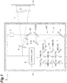
- FIG. 1 is a schematic view illustrating an arrangement of a display device according to an embodiment.
- a display device 1 is a scanning-projection display device that scans a screen S with laser light L and forms a projection image G.
- the display device 1 is applied to, for example, a head-up display which is to be mounted on a vehicle.
- the screen S includes, for example, a diffusion plate.
- the projection image G is formed. Displaying the projection image G on the windshield of a vehicle enables a user to visualize the image projected on the windshield while making the image superimposed on the background.
- the display device 1 includes, as illustrated in FIG. 1 , a light source unit 2 that outputs the laser light L, a light-guide optical system 3 that forms a plurality of optical paths of the laser light L, an optical path switch element 4 that switches an optical path of the laser light L to any of the plurality of optical paths, an optical member 5 that forms a single optical path in a subsequent stage of the plurality of optical paths, a projection mirror 6 that allows scanning with the laser light L to form the projection image G, a light receiving element 7 that detects the laser light L, and a control unit 8 that controls driving of the display device 1.
- a light source unit 2 that outputs the laser light L
- a light-guide optical system 3 that forms a plurality of optical paths of the laser light L
- an optical path switch element 4 that switches an optical path of the laser light L to any of the plurality of optical paths
- an optical member 5 that forms a single optical path in a subsequent stage of the plurality of optical paths
- a projection mirror 6 that allows scanning with the laser light
- the housing 11 includes, for example, aluminum (aluminum die casting alloys such as ADC12) and has a light blocking effect against the laser light L and ambient light.
- ADC12 aluminum die casting alloys
- One surface of the housing 11 is provided with a window member 12 that outputs, toward the screen S, the laser light L used for scanning by the projection mirror 6.
- the window member 12 includes optical glass such as BK7.
- the window member 12 is preferably provided with a thin film or the like which transmits the laser light L and blocks ambient light.
- the light source unit 2 is provided with a unit including a plurality of light sources 13 (13A (red), 13B (green), 13C (blue)) that respectively emits the laser light L corresponding to wavelengths of RGB.
- the light sources 13 include laser diodes (LD), vertical cavity surface emitting lasers (VCSEL), super luminescent diodes (SLD), and light emitting diodes (LED).
- the drive of the light sources 13 is controlled based on control signals from the control unit 8.
- condensers 14 (14A to 14C) are disposed corresponding to the light sources 13A to 13C, respectively.
- dichroic mirrors 15 (15A to 15C) are disposed in a subsequent stage of the condensers 14A to 14C, respectively.
- the condensers 14 are, for example, convex lens, elements that collect the laser light L on the screen S.
- the condensers 14A to 14C are disposed close to the light sources 13A to 13C, respectively, but the condensers 14 may be disposed in any place as long as they are on an optical path between the light sources 13 and the projection mirror 6.
- the dichroic mirrors 15A to 15C are included a multiplexing optical system 16 that multiplexes the laser light L output from the light sources 13A to 13C.
- the laser light L output from the light sources 13A to 13C are made coaxial by the dichroic mirrors 15A to 15C through the condensers 14A to 14C and is guided to the optical path switch element 4.
- the light-guide optical system 3 is an optical system that forms two optical paths, an optical path for low luminance M1 and an optical path for high luminance M2, which makes the laser light L have different luminance.
- the optical path for low luminance M1 includes the optical path switch element 4 and mirrors (luminance attenuation elements) 21A and 21B.
- the optical path for high luminance M2 includes the optical path switch element 4 and one mirror 21B.
- the optical path switch element 4 is an element disposed on an optical path between the light source unit 2 and the projection mirror 6. Examples of the optical path switch element 4 include a micro electro mechanical systems (MEMS) mirror and a polygon mirror.
- MEMS micro electro mechanical systems
- the optical path switch element 4 is driven based on a control signal from the control unit 8 and guides the laser light L from the light source unit 2 to one of the optical path for low luminance M1 and the optical path for high luminance M2.
- Each of the mirrors 21A and 21B is a partial reflection mirror that reflects part of the laser light L and transmits the most part.
- the optical path switch element 4 guides the laser light L to the optical path for low luminance M1
- the laser light L is greatly attenuated by being reflected by each of the mirror 21A and the mirror 21B.
- the optical path switch element 4 guides the laser light L to the optical path for high luminance M2
- the laser light L passes through the mirror 21B without being attenuated that much.
- a component transmitted through the mirror 21B is blocked by a wall of the housing 11.
- the mirror 21B has an attenuation factor of 50% or more, and the luminance attenuation element in a preceding stage of the mirror 21B (mirror 21A in this case) in the optical path for low luminance M1 preferably has an attenuation factor of 50% or more.
- an attenuation factor of 50% or more may be achieved by the plurality of luminance attenuation elements.
- the optical member 5 includes the mirror 21B.
- This mirror 21B forms a single optical path for the laser light L disposed in a subsequent stage of the optical path for low luminance M1 and the optical path for high luminance M2.
- the laser light L that has passed through the optical path for low luminance M1 and the laser light L that has passed through the optical path for high luminance M2 become coaxial in a subsequent stage of the mirror 21B and become the same optical path.
- a partial transmission mirror 23 is disposed, as a reflection unit that bends the optical paths of the laser light L, in the subsequent stage of the mirror 21B.
- the partial transmission mirror 23 is an element that transmits part of the laser light L and reflects the most part.
- the laser light L reflected by the partial transmission mirror 23 is guided to the projection mirror 6.
- the partial transmission mirror 23 bends the optical paths of the laser light L from the mirror 21B at a predetermined angle, which enables downsizing of the device.
- the partial transmission mirror 23 may be omitted.
- an aperture 22 corresponding to a light diameter of the laser light L is disposed on an optical path between the optical member 5 and the projection mirror 6.
- the aperture 22 is disposed between the partial transmission mirror 23 and the projection mirror 6. If an optical axis shift of the laser light L from the optical member 5 occurs, a component of the laser light L in a portion with an optical axis shift is blocked by the aperture 22.
- the aperture 22 may be disposed between the optical path switch element 4 and the projection mirror 6.
- the aperture 22 may be disposed between the mirror 21B and the partial transmission mirror 23 or may be disposed in each of the optical path for low luminance M1 and the optical path for high luminance M2.
- the projection mirror 6 is an element that allows scanning of the screen S with the laser light L that has passed through the single optical path, thereby forming the projection image G which is to be projected on the screen S.
- Examples of the projection mirror 6 include a micro electro mechanical systems (MEMS) mirror and a polygon mirror.
- the projection mirror 6 oscillates at a predetermined frequency based on a control signal from the control unit 8. Oscillation of the projection mirror 6 allows scanning of the screen S with the laser light L output to the outside of the housing 11 through the window member 12 and leads to formation of the projection image G on the screen S.
- MEMS micro electro mechanical systems
- the light receiving element 7 is an element that monitors an optical axis and a light intensity of the laser light L.
- An example of the light receiving element 7 includes a PIN photodiode.
- the light receiving element 7 is disposed in a subsequent stage of the optical member 5 and detects, in regard to the laser light L that has passed through the optical path for low luminance M1, at least a component transmitted through the partial transmission mirror 23.
- the light receiving element 7 generates information indicating a detection result of the laser light L and outputs the result to the control unit 8.
- the display device 1 in detecting the laser light L with low luminance, from a viewpoint of avoiding influences of unnecessary light including ambient light, it is preferable that the display device 1 be provided with a band pass filter or the like in a preceding stage of the light receiving element 7. Furthermore, the display device 1 may be provided with a plurality of light receiving elements 7 that separately detects the laser light L of each of RGB. In this case, one of RGB may be set in advance as a reference color, and after an output of the laser light L of the reference color is adjusted, an output of the laser light L of another color may be adjusted according to the output. When a light intensity of the laser light L is detected by the light receiving element 7, a signal may be multiplied on a circuit of the light receiving element 7, and the multiplied value may be used as the detection result.
- the control unit 8 is, physically, a computer that includes a memory such as RAM and ROM, a processor (arithmetic circuit) such as a CPU, a storage unit such as a communication interface and a hard disk, and a display unit such as a display. Examples of such computer include personal computers, cloud servers, and smart devices (such as smart phones and tablet terminals).
- the computer causes the CPU to execute a program stored in the memory and executes the following functional processing.
- the control unit 8 is, functionally, a section that controls driving of the light sources 13, the optical path switch element 4, and the projection mirror 6.
- the control unit 8 receives detection information associated with the brightness outside a vehicle from, for example, a brightness sensor disposed outside the device. Based on the detection information, the control unit 8 combines the output control of the laser light L in the light source unit 2 and the switching control of the optical paths of the laser light L in the optical path switch element 4 so as to control the luminance of the projection image G, thereby achieving the visibility of the projection image G.
- the control unit 8 controls the output of the laser light L and causes the laser light L to pass through one of the optical path for low luminance M1 and the optical path for high luminance M2 so as to change the luminance of the projection image G.
- the control unit 8 switches the optical path of the laser light L to the optical path for high luminance M2 and increases the luminance of the projection image G.
- the control unit 8 switches the optical path of the laser light L to the optical path for low luminance M1 and decreases the luminance of the projection image G sufficiently.
- the luminance of the projection image G is controlled by the output control of the laser light L in the light source unit 2 and the switching control of the optical paths of the laser light L in the optical path switch element 4.
- Such control sufficiently enhances a dimming ratio of the projection image G.
- at least the optical path for low luminance M1 among the plurality of optical paths include a plurality of mirrors (luminance attenuation elements) 21A and 21B.
- a desired amount of attenuation of the laser light L may be achieved by the plurality of luminance attenuation elements. Accordingly, there is no need to provide one luminance attenuation element with excessive attenuation characteristics, which enables stable luminance attenuation.
- the optical path for low luminance M1 includes one mirror, it is necessary to provide the mirror with high attenuation characteristics. However, it is difficult to stably manufacture a mirror having an attenuation factor of 99% or more (transmittance of 99% or more, or reflectance of 1% or less). Furthermore, in a case where the optical path for low luminance M1 includes one mirror having transmittance of 99% or less, assuming that the intensity of the laser light L is controlled within a range from 1 mW to 100 mW, the dimming ratio becomes 9900 : 1 at a maximum.
- the laser light L output from the light source 13A is controlled to have intensity from 2 mW to 200 mW
- the laser light L output from each of the light source 13B (green) and the light source 13C is controlled to have an intensity from 1 mW to 100 mW.
- a dimming ratio is about 10000 : 1.
- changing the characteristics of the mirror 21A and the mirror 21B makes it possible to switch between the optical path for low luminance M1 and the optical path for high luminance M2.
- a dimming ratio is about 9900 : 1.
- the optical path switch element 4 that switches between the optical path for low luminance M1 and the optical path for high luminance M2 is disposed on an optical path between the light source unit 2 and the projection mirror 6. Since the optical path switch element 4 is disposed in a preceding stage of the projection mirror 6, it is possible to control the luminance by switching the optical paths before the scanning laser light L is spread by the projection mirror 6. This makes it possible to avoid enlargement of a device as compared with a device in which light sources having different luminance are disposed separately or a device which makes a light attenuation unit move back and forth relative to an optical path of laser light. This arrangement also prevents an increase in optical path length due to the optical path for low luminance M1 and the optical path for high luminance M2. Prevention of an increase in optical path length prevents enlargement of the condenser 14 that collects the laser light L on the screen S.
- the condenser 14 that collects the laser light L on the screen S is disposed between the light sources 13 and the projection mirror 6. This arrangement makes it possible to collect the laser light L at a position on the screen S and to display the high-resolution projection image G.
- the light source unit 2 includes the plurality of light sources 13A to 13C which outputs the laser light L having different wavelengths. Accordingly, the projection image G is formed by the laser light L corresponding to, for example, each of RGB. Furthermore, the display device 1 is provided with the multiplexing optical system 16 that multiplexes the laser light L output from the plurality of light sources 13A to 13C. This arrangement standardizes the optical paths of the laser light L even when the plurality of light sources 13A to 13C is used, which enables downsizing of the device.
- the aperture 22 is disposed between the optical path switch element 4 and the projection mirror 6.
- An angle shift of the optical path switch element 4 may cause an optical axis shift of the laser light L in a subsequent stage of the optical path switch element 4.
- incidence of the laser light L upon the projection mirror 6 may cause stray light.
- Disposing the aperture 22 between the optical path switch element 4 and the projection mirror 6 makes it possible for a component of the laser light L in a portion where the optical axis is shifted to be blocked by the aperture 22, which leads to prevention of stray light.
- the aperture 22 is disposed between the optical member 5 (mirror 21B) and the projection mirror 6.
- the optical axis shift of the laser light L due to refraction is caused in the optical member 5
- incidence of the laser light L upon the projection mirror 6 with the optical axis shift may cause stray light.
- Disposing the aperture 22 between the optical path switch element 4 and the projection mirror 6 makes it possible for a component of the laser light L in a portion where the optical axis is shifted to be blocked by the aperture 22, which leads to prevention of stray light.
- the light receiving element 7 that detects the laser light L that has passed through at least the optical path for low luminance is disposed in the subsequent stage of the optical member 5. Monitoring a position of the optical axis of the laser light L with the light receiving element 7 makes it possible to prevent stray light more reliably. Furthermore, monitoring a light intensity of the laser light L with the light receiving element 7 makes it possible to stably control the luminance of the projection image G. Particularly, since an amount of attenuation of the laser light is larger in the optical path for low luminance M1 than in the optical path for high luminance M2, it is useful to monitor a light intensity of the laser light L with the light receiving element 7. It should be noted that the light receiving element 7 may detect one of a light intensity of the laser light L and a position of the optical axis of the laser light L.
- the optical path for low luminance M1 includes the mirrors 21A and 21B
- the optical path for high luminance M2 includes the mirror 21B
- the number of the luminance attenuation elements included in the optical path for low luminance M1 and the optical path for high luminance M2 may be any number.
- a partial reflection mirror 21C may be additionally disposed in the optical path for high luminance M2.
- the partial reflection mirror 21C may be disposed between the mirror 21B and the partial transmission mirror 23.
- an element that absorbs part of energy of the laser light L such as an attenuation filter, may be disposed as a luminance attenuation element in the display device 1.
- partial reflection mirrors 21D and 21E may be additionally disposed in the optical path for low luminance M1 so as to attenuate the laser light L in a stepwise manner.
- two or more luminance attenuation units are provided in a preceding stage of the mirror 21B in the optical path for low luminance M1, and this arrangement enables reduction of attenuation factor in each luminance attenuation element. Therefore, it is possible to reduce burden in manufacturing of each luminance attenuation element. Furthermore, even if there is a manufacturing error in attenuation factor, decreasing the attenuation factor of each luminance attenuation element makes deviation from desired luminance smaller.
- the display device 1 may be further provided with a component that corrects an optical path length difference between the optical path for low luminance M1 and the optical path for high luminance M2.
- an optical path correcting element 31 may be disposed in the optical path for high luminance M2, and as illustrated in FIG. 5 , mirrors 21F and 21G that form a delay circuit may be disposed in the optical path for high luminance M2.
- An example of the optical path correcting element 31 includes optical glass such as BK7.
- the optical path length difference between the optical path for low luminance M1 and the optical path for high luminance M2 is corrected, which enables a low-luminance display and a high-luminance display to come to a focus, thus making it possible to prevent degradation in quality of the projection image G.
- the display device 1 may be further provided with a component that prevents an optical axis shift of the laser light L due to the mirror 21B.
- a prism 32 may be disposed as the optical member 5 in such a manner that the laser light L from the optical path for low luminance M1 and the laser light L from the optical path for high luminance M2 enter the prism 32. According to such an arrangement, incidence of the laser light L upon the prism 32 in a perpendicular manner does not cause an optical axis shift due to refraction. Accordingly, it is possible to prevent stray light and color shift due to the optical axis shift.
- the prism 32 may function as a luminance attenuation element.
- the prism 32 may be a prism that attenuates the laser light L passing through the optical path for low luminance M1 by 50% or more.
- the optical path for high luminance M2 may be provided with a mirror 21H that cancels out an optical axis shift of the laser light L due to the mirror 21B.
- a mirror 21H that cancels out an optical axis shift of the laser light L due to the mirror 21B.
- a positional relationship between the projection mirror 6 and the light receiving element 7 may be changed.
- an example illustrated in FIG. 8 employs a partial reflection mirror 25 that reflects part of the laser light L and transmits the most part.
- a positional relationship between the projection mirror 6, the aperture 22, and the light receiving element 7 is inversion of the arrangement illustrated in FIG. 1 .
- the light receiving element 7 is disposed in the subsequent stage of the optical member 5.
- a plurality of light receiving elements 7 having different ranges of light intensity detection may be disposed in the subsequent stage of the optical member 5.
- a light intensity of the laser light L passing through the optical path for low luminance M1 may be detected by the light receiving element 7 disposed in the subsequent stage of the optical member 5, and a light intensity of the laser light L passing through the optical path for high luminance M2 may be detected by the light receiving element disposed close to the light sources 13.
- the range of light intensity detection is expanded. Accordingly, it is possible to detect a light intensity even when the dimming ratio is enhanced.
- the embodiment illustrates the display device 1 applied to a head-up display which is to be mounted on a vehicle, but the display device 1 may also be applied to devices other than the head-up display.
- the control unit 8 may execute switching control of the optical paths of the laser light L according to not only the brightness outside a vehicle but also the brightness of environmental light including the brightness outside the vehicle.
- the display device 1 may not be necessarily provided with the light receiving element 7. In a case where the light receiving element 7 is omitted, a high reflection mirror or the like may be disposed in the display device 1 in place of the partial transmission mirror 23.
Landscapes
- Physics & Mathematics (AREA)
- General Physics & Mathematics (AREA)
- Optics & Photonics (AREA)
- Engineering & Computer Science (AREA)
- Multimedia (AREA)
- Signal Processing (AREA)
- Computer Hardware Design (AREA)
- Theoretical Computer Science (AREA)
- Transforming Electric Information Into Light Information (AREA)
- Mechanical Optical Scanning Systems (AREA)
- Projection Apparatus (AREA)
- Control Of Indicators Other Than Cathode Ray Tubes (AREA)
- Mechanical Light Control Or Optical Switches (AREA)
Abstract
Description
- This embodiment relates to a display device.
- In recent years, a development of display devices such as head-up displays or head mounted displays has been advanced. Those display devices project a projection image on a display disposed, for example, in front of a user's field of view and display the image while making the image superimposed on the background. From a viewpoint of achieving good visibility, such display devices require adjustment of luminance of a projection image depending on circumstances (particularly, on brightness). Accordingly, such display devices require to have a sufficient dimming ratio (luminance gradient) of a projection image.
- For example, a head-up display device disclosed in
Patent Literature 1 includes a first laser light source that outputs a first laser light having relatively high luminance and a second laser light source that outputs a second laser light having relatively low luminance. This head-up display device in the related art switches the first light source and the second light source depending on circumstances so as to achieve a dimming ratio of a projection image. - A head-up display device disclosed in
Patent Literature 2, for example, is provided with a light attenuation unit such as a filter in a subsequent stage of a light source. A drive unit such as an actuator moves the light attenuation unit back and forth relative to an optical path of laser light so as to achieve a dimming ratio of a projection image. -
- Patent Literature 1: Japanese Unexamined Patent Publication No.
2016-25430 - Patent Literature 2: Japanese Unexamined Patent Publication No.
2015-525899 - A typical laser light source is a device that has difficulty in maintaining stable operation with a low output. A head-up display in the related art adjusts luminance by controlling an output from a laser light source. However, in adjusting luminance by output control of a laser light source, stable operation with a low output remains as an unsolved issue. For this reason, there is a limit on display of a projection image with low luminance, and it is difficult to achieve a sufficient dimming ratio. Furthermore, a device in which two different laser light sources are switched, as disclosed in
Patent Literature 1, may increase in size, and accordingly, cause cost increase. A device provided with a light attenuation unit that moves back and forth relative to an optical path of laser, as disclosed inPatent Literature 2, may also increase in size. - The present invention has been made to solve the above problems, and an object of the present invention is provide a display device that enables enhancement of dimming ratio of a projection image without increasing in size.
- A display device according to this embodiment includes: a light source unit configured to output laser light; a light-guide optical system configured to form a plurality of optical paths of the laser light; an optical path switch element configured to switch an optical path of the laser light to any one of the plurality of optical paths; an optical member configured to form a single optical path in a subsequent stage of the plurality of optical paths; a projection mirror configured to form a projection image to be projected on a screen by scanning the laser light that passed through the single optical path. The plurality of optical paths includes an optical path for low luminance and an optical path for high luminance which make the laser light have different luminance. The optical path switch element is disposed on an optical path between the light source unit and the projection mirror. The display device includes a control unit configured to control luminance of the projection image by controlling the output of the laser light in the light source unit, and controlling the switching of the optical path of the laser light by the optical path switch element.
- In this display device, the luminance of the projection image is controlled by controlling the output of the laser light in the light source unit, and controlling the switching of the optical path of the laser light by the optical path switch element. Such control sufficiently enhances a dimming ratio of the projection image. In this display device, the optical path switch element that switches between the optical path for low luminance and the optical path for high luminance is disposed on an optical path between the light source unit and the projection mirror. Since the optical path switch element is disposed in a preceding stage of the projection mirror, it is possible to control the luminance by switching the optical paths before the scanning laser light is spread by the projection mirror. This makes it possible to avoid enlargement of a device as compared with a device in which light sources having different luminance are disposed separately or a device which makes a light attenuation unit move back and forth relative to an optical path of laser light.
- In the plurality of optical paths, at least the optical path for low luminance may include a plurality of luminance attenuation elements. In this case, a desired amount of attenuation of the laser light may be achieved by the plurality of luminance attenuation elements. Accordingly, there is no need to provide one luminance attenuation element with excessive attenuation characteristics, which enables stable luminance attenuation.
- In addition, a condenser configured to collect the laser light on the screen may be disposed between the light source unit and the projection mirror. This arrangement makes it possible to display a high-resolution projection image on the screen.
- The light source unit may include a plurality of light sources configured to output laser light having different wavelengths. In this case, the projection image is formed by laser light corresponding to, for example, each of RGB.
- The display device may include a multiplexing optical system configured to multiplex the laser light output from the plurality of light sources. Even when the plurality of light sources is used, this arrangement standardizes the optical paths of the laser light and enables downsizing of the device.
- Furthermore, an aperture may be disposed between the optical path switch element and the projection mirror. An angle shift of the optical path switch element may cause an optical axis shift of the laser light in a subsequent stage of the optical path switch element. With the optical axis shift, incidence of the laser light upon the projection mirror may cause stray light. Disposing the aperture between the optical path switch element and the projection mirror makes it possible to block a component of the laser light in a portion where the optical axis is shifted by the aperture, which leads to prevention of stray light.
- The aperture may be disposed between the optical member and the projection mirror. In a case where an optical axis shift of the laser light due to refraction is caused in the optical member, incidence of the laser light upon the projection mirror with the optical axis shift may cause stray light. Disposing the aperture between the optical member and the projection mirror makes it possible to block a component in which the optical axis is shifted by the aperture, which leads to prevention of stray light. This arrangement is particularly useful when the optical member is inclined relative to the optical axis of the laser light.
- Still further, a light receiving element configured to the laser light may be disposed in a subsequent stage of the optical member. Monitoring a position of the optical axis of the laser light with the light receiving element makes it possible to prevent stray light more reliably. Furthermore, monitoring a light intensity of the laser light with the light receiving element makes it possible to stably control the luminance of the projection image.
- The light receiving element may at least detect the laser light that passed through the optical path for low luminance. Since an amount of attenuation of the laser light is larger in the optical path for low luminance than in the optical path for high luminance, it is particularly useful to monitor a light intensity of the laser light with the light receiving element.
- With this display device, it is possible to enhance a dimming ratio of a projection image without upsizing the device.
-
-
FIG. 1 is a schematic view illustrating an arrangement of a display device according to an embodiment. -
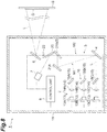
FIG. 2 is a schematic view illustrating an arrangement of a display device according to a modification. -
FIG. 3 is a schematic view illustrating an arrangement of a display device according to another modification. -
FIG. 4 is a schematic view illustrating an arrangement of a display device according to another modification. -
FIG. 5 is a schematic view illustrating an arrangement of a display device according to another modification. -
FIG. 6 is a schematic view illustrating an arrangement of a display device according to another modification. -
FIG. 7 is a schematic view illustrating an arrangement of a display device according to another modification. -
FIG. 8 is a schematic view illustrating an arrangement of a display device according to another modification. - With reference to the drawings, preferred embodiments of a display device according to an aspect of the present invention will now be described in detail.
-
FIG. 1 is a schematic view illustrating an arrangement of a display device according to an embodiment. Adisplay device 1 is a scanning-projection display device that scans a screen S with laser light L and forms a projection image G. Thedisplay device 1 is applied to, for example, a head-up display which is to be mounted on a vehicle. The screen S includes, for example, a diffusion plate. When the laser light L modulated by a predetermined projection signal is projected on the diffusion plate, the projection image G is formed. Displaying the projection image G on the windshield of a vehicle enables a user to visualize the image projected on the windshield while making the image superimposed on the background. - The
display device 1 includes, as illustrated inFIG. 1 , alight source unit 2 that outputs the laser light L, a light-guideoptical system 3 that forms a plurality of optical paths of the laser light L, an optical path switchelement 4 that switches an optical path of the laser light L to any of the plurality of optical paths, anoptical member 5 that forms a single optical path in a subsequent stage of the plurality of optical paths, aprojection mirror 6 that allows scanning with the laser light L to form the projection image G, alight receiving element 7 that detects the laser light L, and acontrol unit 8 that controls driving of thedisplay device 1. - These components are provided, for example, on a substrate (not illustrated) disposed inside a
housing 11. Thehousing 11 includes, for example, aluminum (aluminum die casting alloys such as ADC12) and has a light blocking effect against the laser light L and ambient light. One surface of thehousing 11 is provided with a window member 12 that outputs, toward the screen S, the laser light L used for scanning by theprojection mirror 6. The window member 12 includes optical glass such as BK7. The window member 12 is preferably provided with a thin film or the like which transmits the laser light L and blocks ambient light. - The
light source unit 2 is provided with a unit including a plurality of light sources 13 (13A (red), 13B (green), 13C (blue)) that respectively emits the laser light L corresponding to wavelengths of RGB. Examples of thelight sources 13 include laser diodes (LD), vertical cavity surface emitting lasers (VCSEL), super luminescent diodes (SLD), and light emitting diodes (LED). The drive of thelight sources 13 is controlled based on control signals from thecontrol unit 8. - In the
light source unit 2, condensers 14 (14A to 14C) are disposed corresponding to thelight sources 13A to 13C, respectively. In addition, dichroic mirrors 15 (15A to 15C) are disposed in a subsequent stage of thecondensers 14A to 14C, respectively. Thecondensers 14 are, for example, convex lens, elements that collect the laser light L on the screen S. In this embodiment, thecondensers 14A to 14C are disposed close to thelight sources 13A to 13C, respectively, but thecondensers 14 may be disposed in any place as long as they are on an optical path between thelight sources 13 and theprojection mirror 6. - The dichroic mirrors 15A to 15C are included a multiplexing
optical system 16 that multiplexes the laser light L output from thelight sources 13A to 13C. The laser light L output from thelight sources 13A to 13C are made coaxial by thedichroic mirrors 15A to 15C through thecondensers 14A to 14C and is guided to the optical path switchelement 4. - In this embodiment, the light-guide
optical system 3 is an optical system that forms two optical paths, an optical path for low luminance M1 and an optical path for high luminance M2, which makes the laser light L have different luminance. The optical path for low luminance M1 includes the optical path switchelement 4 and mirrors (luminance attenuation elements) 21A and 21B. On the other hand, the optical path for high luminance M2 includes the optical path switchelement 4 and onemirror 21B. The optical path switchelement 4 is an element disposed on an optical path between thelight source unit 2 and theprojection mirror 6. Examples of the optical path switchelement 4 include a micro electro mechanical systems (MEMS) mirror and a polygon mirror. The optical path switchelement 4 is driven based on a control signal from thecontrol unit 8 and guides the laser light L from thelight source unit 2 to one of the optical path for low luminance M1 and the optical path for high luminance M2. - Each of the
mirrors element 4 guides the laser light L to the optical path for low luminance M1, the laser light L is greatly attenuated by being reflected by each of themirror 21A and themirror 21B. When the optical path switchelement 4 guides the laser light L to the optical path for high luminance M2, the laser light L passes through themirror 21B without being attenuated that much. In the laser light L that passes through the optical path for low luminance M1, a component transmitted through themirror 21B is blocked by a wall of thehousing 11. - The
mirror 21B has an attenuation factor of 50% or more, and the luminance attenuation element in a preceding stage of themirror 21B (mirror 21A in this case) in the optical path for low luminance M1 preferably has an attenuation factor of 50% or more. In a case where a plurality of luminance attenuation elements is disposed in the preceding stage of themirror 21B, an attenuation factor of 50% or more may be achieved by the plurality of luminance attenuation elements. - In this embodiment, the
optical member 5 includes themirror 21B. Thismirror 21B forms a single optical path for the laser light L disposed in a subsequent stage of the optical path for low luminance M1 and the optical path for high luminance M2. In other words, the laser light L that has passed through the optical path for low luminance M1 and the laser light L that has passed through the optical path for high luminance M2 become coaxial in a subsequent stage of themirror 21B and become the same optical path. In addition, apartial transmission mirror 23 is disposed, as a reflection unit that bends the optical paths of the laser light L, in the subsequent stage of themirror 21B. Thepartial transmission mirror 23 is an element that transmits part of the laser light L and reflects the most part. The laser light L reflected by thepartial transmission mirror 23 is guided to theprojection mirror 6. Thepartial transmission mirror 23 bends the optical paths of the laser light L from themirror 21B at a predetermined angle, which enables downsizing of the device. However, thepartial transmission mirror 23 may be omitted. - Furthermore, an
aperture 22 corresponding to a light diameter of the laser light L is disposed on an optical path between theoptical member 5 and theprojection mirror 6. In this embodiment, theaperture 22 is disposed between thepartial transmission mirror 23 and theprojection mirror 6. If an optical axis shift of the laser light L from theoptical member 5 occurs, a component of the laser light L in a portion with an optical axis shift is blocked by theaperture 22. It should be noted that theaperture 22 may be disposed between the optical path switchelement 4 and theprojection mirror 6. Theaperture 22 may be disposed between themirror 21B and thepartial transmission mirror 23 or may be disposed in each of the optical path for low luminance M1 and the optical path for high luminance M2. - The
projection mirror 6 is an element that allows scanning of the screen S with the laser light L that has passed through the single optical path, thereby forming the projection image G which is to be projected on the screen S. Examples of theprojection mirror 6 include a micro electro mechanical systems (MEMS) mirror and a polygon mirror. Theprojection mirror 6 oscillates at a predetermined frequency based on a control signal from thecontrol unit 8. Oscillation of theprojection mirror 6 allows scanning of the screen S with the laser light L output to the outside of thehousing 11 through the window member 12 and leads to formation of the projection image G on the screen S. - The
light receiving element 7 is an element that monitors an optical axis and a light intensity of the laser light L. An example of thelight receiving element 7 includes a PIN photodiode. Thelight receiving element 7 is disposed in a subsequent stage of theoptical member 5 and detects, in regard to the laser light L that has passed through the optical path for low luminance M1, at least a component transmitted through thepartial transmission mirror 23. Thelight receiving element 7 generates information indicating a detection result of the laser light L and outputs the result to thecontrol unit 8. - Particularly, in detecting the laser light L with low luminance, from a viewpoint of avoiding influences of unnecessary light including ambient light, it is preferable that the
display device 1 be provided with a band pass filter or the like in a preceding stage of thelight receiving element 7. Furthermore, thedisplay device 1 may be provided with a plurality oflight receiving elements 7 that separately detects the laser light L of each of RGB. In this case, one of RGB may be set in advance as a reference color, and after an output of the laser light L of the reference color is adjusted, an output of the laser light L of another color may be adjusted according to the output. When a light intensity of the laser light L is detected by thelight receiving element 7, a signal may be multiplied on a circuit of thelight receiving element 7, and the multiplied value may be used as the detection result. - The
control unit 8 is, physically, a computer that includes a memory such as RAM and ROM, a processor (arithmetic circuit) such as a CPU, a storage unit such as a communication interface and a hard disk, and a display unit such as a display. Examples of such computer include personal computers, cloud servers, and smart devices (such as smart phones and tablet terminals). The computer causes the CPU to execute a program stored in the memory and executes the following functional processing. - The
control unit 8 is, functionally, a section that controls driving of thelight sources 13, the optical path switchelement 4, and theprojection mirror 6. Thecontrol unit 8 receives detection information associated with the brightness outside a vehicle from, for example, a brightness sensor disposed outside the device. Based on the detection information, thecontrol unit 8 combines the output control of the laser light L in thelight source unit 2 and the switching control of the optical paths of the laser light L in the optical path switchelement 4 so as to control the luminance of the projection image G, thereby achieving the visibility of the projection image G. In other words, thecontrol unit 8 controls the output of the laser light L and causes the laser light L to pass through one of the optical path for low luminance M1 and the optical path for high luminance M2 so as to change the luminance of the projection image G. For example, when the outside of the vehicle is bright, thecontrol unit 8 switches the optical path of the laser light L to the optical path for high luminance M2 and increases the luminance of the projection image G. For example, when the outside of the vehicle is dark and the luminance of the projection image G is not sufficiently decreased in the optical path for high luminance M2, thecontrol unit 8 switches the optical path of the laser light L to the optical path for low luminance M1 and decreases the luminance of the projection image G sufficiently. - As described above, in this
display device 1, the luminance of the projection image G is controlled by the output control of the laser light L in thelight source unit 2 and the switching control of the optical paths of the laser light L in the optical path switchelement 4. Such control sufficiently enhances a dimming ratio of the projection image G. In this embodiment, at least the optical path for low luminance M1 among the plurality of optical paths include a plurality of mirrors (luminance attenuation elements) 21A and 21B. In this case, a desired amount of attenuation of the laser light L may be achieved by the plurality of luminance attenuation elements. Accordingly, there is no need to provide one luminance attenuation element with excessive attenuation characteristics, which enables stable luminance attenuation. - When the optical path for low luminance M1 includes one mirror, it is necessary to provide the mirror with high attenuation characteristics. However, it is difficult to stably manufacture a mirror having an attenuation factor of 99% or more (transmittance of 99% or more, or reflectance of 1% or less). Furthermore, in a case where the optical path for low luminance M1 includes one mirror having transmittance of 99% or less, assuming that the intensity of the laser light L is controlled within a range from 1 mW to 100 mW, the dimming ratio becomes 9900 : 1 at a maximum. In contrast, in a case where attenuation is performed by a plurality of mirrors, a mirror with excessive attenuation characteristics is not required, and using a mirror with an attenuation factor that enables stable manufacturing offers a dimming ratio of 10000 : 1 or more. In addition, in the case where attenuation is performed by the plurality of mirrors, even if each mirror has a manufacturing error in attenuation factor, deviation of the luminance from desired luminance is made smaller. Accordingly, it is possible to reduce burden in manufacturing.
- For example, assume that the laser light L output from the
light source 13A (red) is controlled to have intensity from 2 mW to 200 mW, and the laser light L output from each of thelight source 13B (green) and thelight source 13C (blue) is controlled to have an intensity from 1 mW to 100 mW. In this case, when themirror 21A has reflectance of 4.0% with respect to the laser light L of each of RGB, and themirror 21B has reflectance of 20.0% and transmittance of 80.0%, a dimming ratio is about 10000 : 1. Furthermore, changing the characteristics of themirror 21A and themirror 21B makes it possible to switch between the optical path for low luminance M1 and the optical path for high luminance M2. In this case, when themirror 21A has reflectance of 100.0% , and themirror 21B has reflectance of 99.0% and transmittance of 1.0%, a dimming ratio is about 9900 : 1. - In this
display device 1, the optical path switchelement 4 that switches between the optical path for low luminance M1 and the optical path for high luminance M2 is disposed on an optical path between thelight source unit 2 and theprojection mirror 6. Since the optical path switchelement 4 is disposed in a preceding stage of theprojection mirror 6, it is possible to control the luminance by switching the optical paths before the scanning laser light L is spread by theprojection mirror 6. This makes it possible to avoid enlargement of a device as compared with a device in which light sources having different luminance are disposed separately or a device which makes a light attenuation unit move back and forth relative to an optical path of laser light. This arrangement also prevents an increase in optical path length due to the optical path for low luminance M1 and the optical path for high luminance M2. Prevention of an increase in optical path length prevents enlargement of thecondenser 14 that collects the laser light L on the screen S. - In the
display device 1, thecondenser 14 that collects the laser light L on the screen S is disposed between thelight sources 13 and theprojection mirror 6. This arrangement makes it possible to collect the laser light L at a position on the screen S and to display the high-resolution projection image G. - In the
display device 1, thelight source unit 2 includes the plurality oflight sources 13A to 13C which outputs the laser light L having different wavelengths. Accordingly, the projection image G is formed by the laser light L corresponding to, for example, each of RGB. Furthermore, thedisplay device 1 is provided with the multiplexingoptical system 16 that multiplexes the laser light L output from the plurality oflight sources 13A to 13C. This arrangement standardizes the optical paths of the laser light L even when the plurality oflight sources 13A to 13C is used, which enables downsizing of the device. - In addition, in the
display device 1, theaperture 22 is disposed between the optical path switchelement 4 and theprojection mirror 6. An angle shift of the optical path switchelement 4 may cause an optical axis shift of the laser light L in a subsequent stage of the optical path switchelement 4. With an optical axis shift, incidence of the laser light L upon theprojection mirror 6 may cause stray light. Disposing theaperture 22 between the optical path switchelement 4 and theprojection mirror 6 makes it possible for a component of the laser light L in a portion where the optical axis is shifted to be blocked by theaperture 22, which leads to prevention of stray light. - In this embodiment, the
aperture 22 is disposed between the optical member 5 (mirror 21B) and theprojection mirror 6. In a case where the optical axis shift of the laser light L due to refraction is caused in theoptical member 5, incidence of the laser light L upon theprojection mirror 6 with the optical axis shift may cause stray light. Disposing theaperture 22 between the optical path switchelement 4 and theprojection mirror 6 makes it possible for a component of the laser light L in a portion where the optical axis is shifted to be blocked by theaperture 22, which leads to prevention of stray light. Furthermore, it is possible to prevent degradation of quality of the projection image G attributed to a color shift caused by the optical axis shift. This arrangement is particularly useful when theoptical member 5 is inclined relative to the optical axis of the laser light L. - In the
display device 1, thelight receiving element 7 that detects the laser light L that has passed through at least the optical path for low luminance is disposed in the subsequent stage of theoptical member 5. Monitoring a position of the optical axis of the laser light L with thelight receiving element 7 makes it possible to prevent stray light more reliably. Furthermore, monitoring a light intensity of the laser light L with thelight receiving element 7 makes it possible to stably control the luminance of the projection image G. Particularly, since an amount of attenuation of the laser light is larger in the optical path for low luminance M1 than in the optical path for high luminance M2, it is useful to monitor a light intensity of the laser light L with thelight receiving element 7. It should be noted that thelight receiving element 7 may detect one of a light intensity of the laser light L and a position of the optical axis of the laser light L. - The present invention should not be restricted to the aforementioned embodiment. For example, in the embodiment, the optical path for low luminance M1 includes the
mirrors mirror 21B, but the number of the luminance attenuation elements included in the optical path for low luminance M1 and the optical path for high luminance M2 may be any number. For example, as illustrated inFIG. 2 , apartial reflection mirror 21C may be additionally disposed in the optical path for high luminance M2. Thepartial reflection mirror 21C may be disposed between themirror 21B and thepartial transmission mirror 23. With such an arrangement in which the luminance of the laser light L is attenuated by a plurality of mirrors, even if there is a manufacturing error in attenuation factor, it is possible to reduce deviation from desired luminance. In the example ofFIG. 2 , in place of thepartial reflection mirror 21C, an element that absorbs part of energy of the laser light L, such as an attenuation filter, may be disposed as a luminance attenuation element in thedisplay device 1. - In addition, as illustrated in
FIG. 3 , for example, partial reflection mirrors 21D and 21E may be additionally disposed in the optical path for low luminance M1 so as to attenuate the laser light L in a stepwise manner. According to such an arrangement, two or more luminance attenuation units are provided in a preceding stage of themirror 21B in the optical path for low luminance M1, and this arrangement enables reduction of attenuation factor in each luminance attenuation element. Therefore, it is possible to reduce burden in manufacturing of each luminance attenuation element. Furthermore, even if there is a manufacturing error in attenuation factor, decreasing the attenuation factor of each luminance attenuation element makes deviation from desired luminance smaller. - The
display device 1 may be further provided with a component that corrects an optical path length difference between the optical path for low luminance M1 and the optical path for high luminance M2. In this case, for example, as illustrated inFIG. 4 , an opticalpath correcting element 31 may be disposed in the optical path for high luminance M2, and as illustrated inFIG. 5 , mirrors 21F and 21G that form a delay circuit may be disposed in the optical path for high luminance M2. An example of the opticalpath correcting element 31 includes optical glass such as BK7. According to these arrangements, the optical path length difference between the optical path for low luminance M1 and the optical path for high luminance M2 is corrected, which enables a low-luminance display and a high-luminance display to come to a focus, thus making it possible to prevent degradation in quality of the projection image G. - The
display device 1 may be further provided with a component that prevents an optical axis shift of the laser light L due to themirror 21B. In this case, for example, as illustrated inFIG. 6 , in place of themirror 21B, aprism 32 may be disposed as theoptical member 5 in such a manner that the laser light L from the optical path for low luminance M1 and the laser light L from the optical path for high luminance M2 enter theprism 32. According to such an arrangement, incidence of the laser light L upon theprism 32 in a perpendicular manner does not cause an optical axis shift due to refraction. Accordingly, it is possible to prevent stray light and color shift due to the optical axis shift. Theprism 32 may function as a luminance attenuation element. For example, theprism 32 may be a prism that attenuates the laser light L passing through the optical path for low luminance M1 by 50% or more. - Furthermore, for example, as illustrated in
FIG. 7 , the optical path for high luminance M2 may be provided with amirror 21H that cancels out an optical axis shift of the laser light L due to themirror 21B. Such an arrangement allows themirror 21H to cancel out influences of the refraction of the laser light L on themirror 21B, which enables correction of the optical axis shift. - Still further, a positional relationship between the
projection mirror 6 and thelight receiving element 7 may be changed. In place of thepartial transmission mirror 23 inFIG. 1 and the like, an example illustrated inFIG. 8 employs apartial reflection mirror 25 that reflects part of the laser light L and transmits the most part. In this example, a positional relationship between theprojection mirror 6, theaperture 22, and thelight receiving element 7 is inversion of the arrangement illustrated inFIG. 1 . With such an arrangement in which the positional relationship between theprojection mirror 6 and thelight receiving element 7 is inversed, an optical path length up to the screen S is reduced. Accordingly, it is possible to prevent enlargement of thecondenser 14. - In the embodiment, the
light receiving element 7 is disposed in the subsequent stage of theoptical member 5. However, in a case where a wide range of light intensity detection is required in thelight receiving element 7 due to enhancement in dimming ratio, a plurality oflight receiving elements 7 having different ranges of light intensity detection may be disposed in the subsequent stage of theoptical member 5. In this case, for example, a light intensity of the laser light L passing through the optical path for low luminance M1 may be detected by thelight receiving element 7 disposed in the subsequent stage of theoptical member 5, and a light intensity of the laser light L passing through the optical path for high luminance M2 may be detected by the light receiving element disposed close to thelight sources 13. With such an arrangement in which the light receiving elements for the laser light L passing through the optical path for low luminance M1 and the laser light L passing through the optical path for high luminance are provided in thedisplay device 1, the range of light intensity detection is expanded. Accordingly, it is possible to detect a light intensity even when the dimming ratio is enhanced. - The embodiment illustrates the
display device 1 applied to a head-up display which is to be mounted on a vehicle, but thedisplay device 1 may also be applied to devices other than the head-up display. In this case, thecontrol unit 8 may execute switching control of the optical paths of the laser light L according to not only the brightness outside a vehicle but also the brightness of environmental light including the brightness outside the vehicle. Furthermore, thedisplay device 1 may not be necessarily provided with thelight receiving element 7. In a case where thelight receiving element 7 is omitted, a high reflection mirror or the like may be disposed in thedisplay device 1 in place of thepartial transmission mirror 23. -
- 1
- display device
- 2
- light source unit
- 3
- light-guide optical system
- 4
- optical path switch element
- 5
- optical member
- 6
- projection mirror
- 7
- light receiving element
- 8
- control unit
- 13 (13A to 13C)
- light source
- 14 (14A to 14C)
- condenser
- 21A to 21E
- mirror (luminance attenuation element)
- 22
- aperture
- G
- projection image
- L
- laser light
- M1
- optical path for low luminance
- M2
- optical path for high luminance
- S
- screen
Claims (9)
- A display device comprising:a light source unit configured to output laser light;a light-guide optical system configured to form a plurality of optical paths of the laser light;an optical path switch element configured to switch an optical path of the laser light to any one of the plurality of optical paths;an optical member configured to form a single optical path in a subsequent stage of the plurality of optical paths;a projection mirror configured to form a projection image to be projected on a screen by scanning the laser light that passed through the single optical path,wherein the plurality of optical paths includes an optical path for low luminance and an optical path for high luminance which make the laser light have different luminance,the optical path switch element is disposed on an optical path between the light source unit and the projection mirror, andthe display device comprises a control unit configured to control luminance of the projection image by controlling the output of the laser light in the light source unit, and controlling the switching of the optical path of the laser light by the optical path switch element.
- The display device according to claim 1, wherein, in the plurality of optical paths, at least the optical path for low luminance includes a plurality of luminance attenuation elements.
- The display device according to claim 1 or 2, wherein a condenser lens configured to collect the laser light on the screen is disposed between the light source unit and the projection mirror.
- The display device according to any one of claims 1 to 3, wherein the light source unit includes a plurality of light sources configured to output the laser light having different wavelengths.
- The display device according to claim 4, comprising a multiplexing optical system configured to multiplex the laser light output from the plurality of light sources.
- The display device according to any one of claims 1 to 5, wherein an aperture is disposed between the optical path switch element and the projection mirror.
- The display device according to claim 6, wherein an aperture is disposed between the optical member and the projection mirror.
- The display device according to any one of claims 1 to 7, wherein a light receiving element configured to detect the laser light is disposed in a subsequent stage of the optical member.
- The display device according to claim 8, wherein the light receiving element at least detects the laser light that passed through the optical path for low luminance.
Applications Claiming Priority (2)
| Application Number | Priority Date | Filing Date | Title |
|---|---|---|---|
| JP2017009746A JP6885735B2 (en) | 2017-01-23 | 2017-01-23 | Scanning device |
| PCT/JP2017/038016 WO2018135056A1 (en) | 2017-01-23 | 2017-10-20 | Display device |
Publications (2)
| Publication Number | Publication Date |
|---|---|
| EP3572861A1 true EP3572861A1 (en) | 2019-11-27 |
| EP3572861A4 EP3572861A4 (en) | 2020-10-21 |
Family
ID=62908050
Family Applications (1)
| Application Number | Title | Priority Date | Filing Date |
|---|---|---|---|
| EP17893407.1A Withdrawn EP3572861A4 (en) | 2017-01-23 | 2017-10-20 | DISPLAY DEVICE |
Country Status (6)
| Country | Link |
|---|---|
| US (1) | US11340447B2 (en) |
| EP (1) | EP3572861A4 (en) |
| JP (1) | JP6885735B2 (en) |
| CN (1) | CN110199217B (en) |
| TW (1) | TWI750253B (en) |
| WO (1) | WO2018135056A1 (en) |
Families Citing this family (2)
| Publication number | Priority date | Publication date | Assignee | Title |
|---|---|---|---|---|
| US11966057B2 (en) * | 2020-11-20 | 2024-04-23 | Google Llc | Display system with adjustable field of view |
| US20230185115A1 (en) * | 2021-12-12 | 2023-06-15 | Donaldo Rex Mitogo | "M-tech" |
Family Cites Families (19)
| Publication number | Priority date | Publication date | Assignee | Title |
|---|---|---|---|---|
| US6366386B1 (en) * | 1999-06-17 | 2002-04-02 | Canon Kabushiki Kaisha | Scanning optical device and image forming apparatus using the same |
| JP2005156650A (en) | 2003-11-21 | 2005-06-16 | Hitachi Ltd | Projection-type image display device |
| JP4063213B2 (en) | 2003-12-09 | 2008-03-19 | カシオ計算機株式会社 | LIGHT SOURCE DEVICE AND PROJECTOR HAVING THE SAME |
| CN101233443B (en) | 2005-07-28 | 2010-06-23 | 松下电器产业株式会社 | Laser image display |
| JP4915348B2 (en) * | 2005-12-28 | 2012-04-11 | 株式会社ニコン | Optical scanning device, optical scanning microscope, observation method, control device, and control program |
| EP2037312A4 (en) | 2006-10-11 | 2011-07-20 | Panasonic Corp | LASER DISPLAY DEVICE |
| US7839566B2 (en) * | 2008-06-27 | 2010-11-23 | Carl Zeiss Surgical Gmbh | Surgical microscopy system and imaging method |
| JP2011022524A (en) * | 2009-07-21 | 2011-02-03 | Hitachi Consumer Electronics Co Ltd | Projection video display apparatus |
| JP2011128423A (en) * | 2009-12-18 | 2011-06-30 | Nikon Corp | Scanning microscope, method of controlling the same, and program |
| FR2993677B1 (en) | 2012-07-18 | 2015-03-27 | Valeo Etudes Electroniques | DEVICE AND METHOD FOR TRANSMITTING A LIGHT BEAM FOR FORMING AN IMAGE, PROJECTION SYSTEM AND DISPLAY USING THE SAME |
| JP5975285B2 (en) * | 2012-10-05 | 2016-08-23 | 日本精機株式会社 | Laser scanning display device |
| US20140160439A1 (en) * | 2012-12-10 | 2014-06-12 | Funai Electric Co., Ltd. | Image display device |
| JP2014197041A (en) * | 2013-03-29 | 2014-10-16 | 船井電機株式会社 | Projector |
| JP6387589B2 (en) * | 2013-08-30 | 2018-09-12 | 株式会社リコー | Image forming apparatus, vehicle, and control method of image forming apparatus |
| CN106471417B (en) * | 2014-06-13 | 2019-03-12 | 三菱电机株式会社 | Virtual image display device and vehicle head mounted display |
| JP2016025430A (en) | 2014-07-17 | 2016-02-08 | 船井電機株式会社 | Projector and head-up display device |
| US10338377B1 (en) * | 2015-07-06 | 2019-07-02 | Mirrorcle Technologies, Inc. | Head up display based on laser MEMS emissive film projection system |
| US10852533B2 (en) * | 2015-12-10 | 2020-12-01 | Ricoh Company, Ltd. | Optical scanning device, image display device, and vehicle |
| JP6694742B2 (en) * | 2016-03-25 | 2020-05-20 | 株式会社日立エルジーデータストレージ | Laser projection display |
-
2017
- 2017-01-23 JP JP2017009746A patent/JP6885735B2/en active Active
- 2017-10-20 WO PCT/JP2017/038016 patent/WO2018135056A1/en not_active Ceased
- 2017-10-20 EP EP17893407.1A patent/EP3572861A4/en not_active Withdrawn
- 2017-10-20 CN CN201780084268.XA patent/CN110199217B/en active Active
- 2017-10-20 US US16/478,989 patent/US11340447B2/en active Active
- 2017-11-07 TW TW106138376A patent/TWI750253B/en active
Also Published As
| Publication number | Publication date |
|---|---|
| TWI750253B (en) | 2021-12-21 |
| EP3572861A4 (en) | 2020-10-21 |
| JP2018120030A (en) | 2018-08-02 |
| CN110199217A (en) | 2019-09-03 |
| US20190353895A1 (en) | 2019-11-21 |
| JP6885735B2 (en) | 2021-06-16 |
| CN110199217B (en) | 2021-07-13 |
| WO2018135056A1 (en) | 2018-07-26 |
| US11340447B2 (en) | 2022-05-24 |
| TW201827890A (en) | 2018-08-01 |
Similar Documents
| Publication | Publication Date | Title |
|---|---|---|
| US9462244B2 (en) | Image display apparatus and optical component | |
| CN106200224B (en) | Projection device | |
| KR101646390B1 (en) | Combination structure of Head up display system and Driven State Monitoring | |
| EP3064984B1 (en) | Display device | |
| CN105339831A (en) | Color mixing device and display device | |
| US10194123B2 (en) | Boundary timing controller for display apparatus | |
| JP6197955B2 (en) | Display device, vehicle | |
| US11340447B2 (en) | Scanning device | |
| EP3327707B1 (en) | Light-projecting device | |
| CN109861757A (en) | Control method, time-of-flight component, electronic device and readable storage medium | |
| US10747094B2 (en) | Projection display device, method of controlling projection display device, and program for controlling projection display device | |
| CN111771151A (en) | Laser output control device and laser scanning type display device | |
| CN115339318A (en) | Head-up display with display device | |
| US9952492B2 (en) | Projection-type display device and light source control method therefor | |
| JP2018114909A (en) | Head-up display | |
| US12313855B2 (en) | Systems and methods to separate scanning mirror input and output light | |
| JP6380797B2 (en) | Head-up display device | |
| US11209722B2 (en) | Projection optical system and image projection device | |
| JP2018173437A (en) | Head-up display | |
| JP6926832B2 (en) | Head-up display device | |
| EP4597297A1 (en) | Temperature-based dynamic laser tuning to promote display uniformity | |
| JP2020112710A (en) | Head-up display | |
| US12366699B2 (en) | Coupling narrowband projector source light into display waveguides | |
| JP2017151145A (en) | Light source device and projection device | |
| JP2008058627A (en) | Projector and projection system |
Legal Events
| Date | Code | Title | Description |
|---|---|---|---|
| STAA | Information on the status of an ep patent application or granted ep patent |
Free format text: STATUS: THE INTERNATIONAL PUBLICATION HAS BEEN MADE |
|
| PUAI | Public reference made under article 153(3) epc to a published international application that has entered the european phase |
Free format text: ORIGINAL CODE: 0009012 |
|
| STAA | Information on the status of an ep patent application or granted ep patent |
Free format text: STATUS: REQUEST FOR EXAMINATION WAS MADE |
|
| 17P | Request for examination filed |
Effective date: 20190812 |
|
| AK | Designated contracting states |
Kind code of ref document: A1 Designated state(s): AL AT BE BG CH CY CZ DE DK EE ES FI FR GB GR HR HU IE IS IT LI LT LU LV MC MK MT NL NO PL PT RO RS SE SI SK SM TR |
|
| A4 | Supplementary search report drawn up and despatched |
Effective date: 20200918 |
|
| RIC1 | Information provided on ipc code assigned before grant |
Ipc: H04N 9/31 20060101ALI20200914BHEP Ipc: G02B 26/08 20060101ALI20200914BHEP Ipc: G02B 26/10 20060101AFI20200914BHEP Ipc: H04N 5/74 20060101ALI20200914BHEP Ipc: G02B 27/01 20060101ALI20200914BHEP Ipc: G02B 26/02 20060101ALI20200914BHEP Ipc: G02B 27/18 20060101ALI20200914BHEP Ipc: G02B 27/10 20060101ALI20200914BHEP |
|
| STAA | Information on the status of an ep patent application or granted ep patent |
Free format text: STATUS: EXAMINATION IS IN PROGRESS |
|
| 17Q | First examination report despatched |
Effective date: 20221207 |
|
| GRAP | Despatch of communication of intention to grant a patent |
Free format text: ORIGINAL CODE: EPIDOSNIGR1 |
|
| STAA | Information on the status of an ep patent application or granted ep patent |
Free format text: STATUS: GRANT OF PATENT IS INTENDED |
|
| RIC1 | Information provided on ipc code assigned before grant |
Ipc: G02B 27/14 20060101ALI20241108BHEP Ipc: G02B 5/20 20060101ALI20241108BHEP Ipc: G02B 26/08 20060101ALI20241108BHEP Ipc: G02B 27/18 20060101ALI20241108BHEP Ipc: H04N 5/74 20060101ALI20241108BHEP Ipc: G02B 27/01 20060101ALI20241108BHEP Ipc: G02B 27/10 20060101ALI20241108BHEP Ipc: H04N 9/31 20060101ALI20241108BHEP Ipc: G02B 26/02 20060101ALI20241108BHEP Ipc: G02B 26/10 20060101AFI20241108BHEP |
|
| INTG | Intention to grant announced |
Effective date: 20241121 |
|
| STAA | Information on the status of an ep patent application or granted ep patent |
Free format text: STATUS: THE APPLICATION IS DEEMED TO BE WITHDRAWN |
|
| 18D | Application deemed to be withdrawn |
Effective date: 20250322 |