EP3570317A1 - Area-selective deposition of a mask material - Google Patents
Area-selective deposition of a mask material Download PDFInfo
- Publication number
- EP3570317A1 EP3570317A1 EP18173024.3A EP18173024A EP3570317A1 EP 3570317 A1 EP3570317 A1 EP 3570317A1 EP 18173024 A EP18173024 A EP 18173024A EP 3570317 A1 EP3570317 A1 EP 3570317A1
- Authority
- EP
- European Patent Office
- Prior art keywords
- oxygen
- dielectric material
- line structures
- top surface
- cavity
- Prior art date
- Legal status (The legal status is an assumption and is not a legal conclusion. Google has not performed a legal analysis and makes no representation as to the accuracy of the status listed.)
- Withdrawn
Links
Images


Classifications
-
- H—ELECTRICITY
- H10—SEMICONDUCTOR DEVICES; ELECTRIC SOLID-STATE DEVICES NOT OTHERWISE PROVIDED FOR
- H10D—INORGANIC ELECTRIC SEMICONDUCTOR DEVICES
- H10D30/00—Field-effect transistors [FET]
- H10D30/60—Insulated-gate field-effect transistors [IGFET]
- H10D30/62—Fin field-effect transistors [FinFET]
- H10D30/6219—Fin field-effect transistors [FinFET] characterised by the source or drain electrodes
-
- H—ELECTRICITY
- H10—SEMICONDUCTOR DEVICES; ELECTRIC SOLID-STATE DEVICES NOT OTHERWISE PROVIDED FOR
- H10P—GENERIC PROCESSES OR APPARATUS FOR THE MANUFACTURE OR TREATMENT OF DEVICES COVERED BY CLASS H10
- H10P50/00—Etching of wafers, substrates or parts of devices
- H10P50/73—Etching of wafers, substrates or parts of devices using masks for insulating materials
-
- H—ELECTRICITY
- H10—SEMICONDUCTOR DEVICES; ELECTRIC SOLID-STATE DEVICES NOT OTHERWISE PROVIDED FOR
- H10W—GENERIC PACKAGES, INTERCONNECTIONS, CONNECTORS OR OTHER CONSTRUCTIONAL DETAILS OF DEVICES COVERED BY CLASS H10
- H10W20/00—Interconnections in chips, wafers or substrates
- H10W20/01—Manufacture or treatment
- H10W20/031—Manufacture or treatment of conductive parts of the interconnections
- H10W20/056—Manufacture or treatment of conductive parts of the interconnections by filling conductive material into holes, grooves or trenches
- H10W20/057—Manufacture or treatment of conductive parts of the interconnections by filling conductive material into holes, grooves or trenches by selectively depositing, e.g. by using selective CVD or plating
-
- H—ELECTRICITY
- H10—SEMICONDUCTOR DEVICES; ELECTRIC SOLID-STATE DEVICES NOT OTHERWISE PROVIDED FOR
- H10D—INORGANIC ELECTRIC SEMICONDUCTOR DEVICES
- H10D30/00—Field-effect transistors [FET]
- H10D30/01—Manufacture or treatment
- H10D30/021—Manufacture or treatment of FETs having insulated gates [IGFET]
- H10D30/024—Manufacture or treatment of FETs having insulated gates [IGFET] of fin field-effect transistors [FinFET]
-
- H—ELECTRICITY
- H10—SEMICONDUCTOR DEVICES; ELECTRIC SOLID-STATE DEVICES NOT OTHERWISE PROVIDED FOR
- H10D—INORGANIC ELECTRIC SEMICONDUCTOR DEVICES
- H10D30/00—Field-effect transistors [FET]
- H10D30/60—Insulated-gate field-effect transistors [IGFET]
- H10D30/62—Fin field-effect transistors [FinFET]
-
- H—ELECTRICITY
- H10—SEMICONDUCTOR DEVICES; ELECTRIC SOLID-STATE DEVICES NOT OTHERWISE PROVIDED FOR
- H10D—INORGANIC ELECTRIC SEMICONDUCTOR DEVICES
- H10D64/00—Electrodes of devices having potential barriers
- H10D64/01—Manufacture or treatment
-
- H—ELECTRICITY
- H10—SEMICONDUCTOR DEVICES; ELECTRIC SOLID-STATE DEVICES NOT OTHERWISE PROVIDED FOR
- H10P—GENERIC PROCESSES OR APPARATUS FOR THE MANUFACTURE OR TREATMENT OF DEVICES COVERED BY CLASS H10
- H10P50/00—Etching of wafers, substrates or parts of devices
- H10P50/20—Dry etching; Plasma etching; Reactive-ion etching
- H10P50/28—Dry etching; Plasma etching; Reactive-ion etching of insulating materials
-
- H—ELECTRICITY
- H10—SEMICONDUCTOR DEVICES; ELECTRIC SOLID-STATE DEVICES NOT OTHERWISE PROVIDED FOR
- H10W—GENERIC PACKAGES, INTERCONNECTIONS, CONNECTORS OR OTHER CONSTRUCTIONAL DETAILS OF DEVICES COVERED BY CLASS H10
- H10W20/00—Interconnections in chips, wafers or substrates
- H10W20/01—Manufacture or treatment
- H10W20/031—Manufacture or treatment of conductive parts of the interconnections
- H10W20/069—Manufacture or treatment of conductive parts of the interconnections by forming self-aligned vias or self-aligned contact plugs
-
- H—ELECTRICITY
- H10—SEMICONDUCTOR DEVICES; ELECTRIC SOLID-STATE DEVICES NOT OTHERWISE PROVIDED FOR
- H10P—GENERIC PROCESSES OR APPARATUS FOR THE MANUFACTURE OR TREATMENT OF DEVICES COVERED BY CLASS H10
- H10P14/00—Formation of materials, e.g. in the shape of layers or pillars
- H10P14/40—Formation of materials, e.g. in the shape of layers or pillars of conductive or resistive materials
- H10P14/412—Deposition of metallic or metal-silicide materials
- H10P14/414—Deposition of metallic or metal-silicide materials of metal-silicide materials
Definitions
- the present invention relates to the formation of a cavity in a semiconductor structure, in particular to the formation of such a cavity based on the area-selective deposition of a mask material.
- US6573602B2 discloses a method for forming a self-aligned contact.
- the method uses six distinct insulating layers, two of which are nitride layers functioning as etch stoppers.
- the two nitride insulating layers may be considered as jointly forming a double spacer.
- this plurality of insulating layers results in a relatively thick spacer region, thereby preventing a tight gate spacing.
- a cavity with a high aspect ratio can be made (e.g. a cavity that's is relatively deep compared to its width).
- the cavity can be made while minimizing the damage to surrounding elements in the structure (e.g. to the sidewalls which define the cavity).
- the formation of the cavity can be integrated into fabrication processes for different types of semiconductor structures, including semiconductor devices such as transistors.
- the cavity can be formed in a relatively simple and economical manner.
- an intermediate step in the method can concurrently enable a non-metallic hardmask to be formed. It is a further advantage of embodiments of the present invention that non-metallic hardmask avoid the introduction of metallic contamination in semiconductor structures.
- the present invention relates to a method for forming a cavity in a semiconductor structure, the method comprising:
- the present invention relates to an intermediate structure for forming a cavity in a semiconductor structure, comprising:
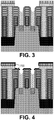
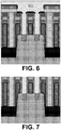
- Figs. 1 to 7 are schematic representations of vertical cross-sections through a semiconductor structure at different steps in a method for forming and subsequently filling a cavity, in accordance with embodiments of the present invention.
- Coupled should not be interpreted as being restricted to direct connections only.
- the terms “coupled” and “connected”, along with their derivatives, may be used. It should be understood that these terms are not intended as synonyms for each other.
- the scope of the expression “a device A coupled to a device B” should not be limited to devices or systems wherein an output of device A is directly connected to an input of device B. It means that there exists a path between an output of A and an input of B which may be a path including other devices or means.
- Coupled may mean that two or more elements are either in direct physical or electrical contact, or that two or more elements are not in direct contact with each other but yet still co-operate or interact with each other.
- an element described herein of an apparatus embodiment is an example of a means for carrying out the function performed by the element for the purpose of carrying out the invention.
- transistors These are devices having a first main electrode such as a drain, a second main electrode such as a source and a control electrode such as a gate for controlling the flow of electrical charges between the first and second main electrodes.
- CMOS complementary metal-oxide-semiconductor
- BICMOS Bipolar complementary metal-oxide-semiconductor
- SiGe BICMOS Bipolar complementary metal-oxide-semiconductor
- first material when a first material is said to be removed or etched selectively with respect to a second material, this means that the first material is removed or etched faster than the second material.
- the removal or etching process would remove or etch the first material at least twice faster, or more preferably at least five times faster, yet more preferably at least ten times faster, than the second material.
- the second material may be substantially not removed or etched by the removal or etching process.
- subscripts 'x' and 'y' in chemical formulae denote a corresponding integer or non-integer subscript number, and said subscript numbers are independently selected from one chemical formula to the next.
- 'x'-values are not necessarily equal; though they could be equal in some embodiments.
- a source and/or drain are understood a 'source and/or drain'.
- a 'source and/or drain entity' e.g. source/drain region
- a 'source entity and/or drain entity' e.g. a source region and/or drain region.
- a source and a drain may be comparable (e.g. indistinguishable) and their designation may depend on a relative voltage difference that is put across them in the final semiconductor device.
- oxygen-free dielectric material refers to a dielectric material which chemical formula does not comprise oxygen, i.e. it is not an oxide (e.g. it might be a nitride).
- oxygen-free is used to express that there is substantially no oxygen in the material.
- oxygen-containing dielectric material refers to a material which chemical formula comprise oxygen, e.g. it is an oxide.
- the present invention relates to a method for forming a cavity in a semiconductor structure, the method comprising:
- the semiconductor structure may typically also be referred to as a semiconductor device.
- the semiconductor structure may, for example, be a structure for forming a semiconductor circuit comprising one or more transistors, such as for forming a complementary metal oxide semiconductor (CMOS) structure.
- CMOS complementary metal oxide semiconductor
- the transistors may, for example, be fin field effect transistors (FinFETs).
- the substrate may comprise at least one semiconductor active area.
- the semiconductor active area may comprise a channel region and/or a source region and/or a drain region.
- the semiconductor active area may comprise one or more materials selected from Si, SiGe and Ge; for example, the channel region and/or the source region and/or the drain region may comprise a material selected from Si, SiGe and Ge.
- the source region and the drain region may define the channel region therebetween.
- the semiconductor active area may comprise a fin structure.
- the fin structure may comprise the channel region, the source region, and the drain region.
- the fin structure may comprise one or more materials selected from Si, SiGe, and Ge.
- a dielectric material may be present between two fin structures.
- the dielectric material may be SiO 2 .
- the dielectric material advantageously provides an electrical isolation between two fin structures.
- the source/drain regions may be epitaxially grown (e.g. in cavities formed in the fin structure) and may optionally be doped.
- the source/drain regions may comprise SiGe:P or SiGe:B.
- At least one of the line structures may comprise:
- the gate structure may comprise a gate dielectric (typically in contact with the semiconductor active area), a work function adjustment metal (i.e. a work function tuning metal) and a gate contact.
- the gate structure may define the channel region in the semiconductor active area it overlaps.
- the gate structure may be formed by a replacement metal gate (RMG) process.
- the gate dielectric may be a high-k material (e.g. HfO 2 ).
- the work function adjustment metal may be selected from TiN, TaN, TiSiN, TiAl and TiC.
- the gate contact may comprise (e.g. consist of) W.
- the gate spacer may comprise the oxygen-free dielectric material.
- the gate spacer may advantageously offer a level of protection (e.g. in a sideways direction) to the gate structure from being damaged (e.g. etched) during steps of the present method and/or further steps for fabricating the final device (e.g. the semiconductor circuit). Additionally, in the final device, the spacer can advantageously provide an electrical isolation between the gate contact on the one hand and a source/drain contact on the other hand.
- the gate spacer may be provided using a chemical vapour deposition (CVD) or an atomic layer deposition (ALD).
- the gate spacer may initially (e.g.
- the gate spacer may ultimately (e.g. after step c or d) have a thickness of from 1 to 10 nm, preferably of from 3 to 8 nm.
- the final (i.e. ultimate) gate spacer thickness for a device at the 7 nm technology node may be about 7 nm, while it may be about 5 nm for further technology nodes (e.g. N5).
- the gate cap may comprise the oxygen-free dielectric material.
- the gate cap may advantageously offer a level of protection (e.g. in a top-down direction) to the gate structure against damages (e.g. during etching) during steps of the present method and further steps for fabricating the final device (e.g. the semiconductor circuit). Additionally, in the final device, the gate cap can advantageously provide an electrical isolation between the gate contact on the one hand and an overlying metallization layer on the other hand.
- the gate cap may be provided using a chemical vapour deposition (CVD) or an atomic layer deposition (ALD), preferably CVD.
- the gate cap may have a height of from 10 to 100 nm, preferably of from 30 to 70 nm.
- the gate spacer and/or the gate plug may be provided using a chemical vapour deposition (CVD) or an atomic layer deposition (ALD).
- CVD chemical vapour deposition
- ALD atomic layer deposition
- both the gate spacer and the gate cap may comprise the oxygen-free dielectric material.
- the oxygen-free dielectric material may be a nitride material, such as silicon nitride (Si x N y ).
- the silicon nitride may be Si 3 N 4 .
- the oxygen-containing dielectric material may be SiO 2 . In embodiments, the oxygen-containing dielectric material may be an interlayer dielectric (ILD).
- ILD interlayer dielectric
- At least one trench may have a width (e.g. a shortest dimension parallel to the substrate) of from 5 to 25 nm, preferably from 10 to 20 nm, such as about 19 nm (e.g. for the N10 node), 14 nm (e.g. for the N7 node) or 11 nm (e.g. for the N5 node).
- at least one trench may have a depth (e.g. a height; a dimension perpendicular to the substrate) of from 20 to 200 nm, preferably from 50 to 100 nm.
- the trenches may be underfilled, or filled such that a top surface of the oxygen-containing dielectric material is coplanar with the top surface of the line structures, or overfilled (e.g. an overburden may be present); so long as the top surface of at least one of the line structures is at least partially exposed, the exposed part being composed of the oxygen-free dielectric material.
- the trenches may be underfilled; for example, filling at least 50% of a trench depth, preferably at least 70%, yet more preferably at least 90%, most preferably at least 95%, but less than 100% of said trench depth.
- providing the trenches being at least partially filled with the oxygen-containing dielectric material may comprise providing trenches fully filled (e.g.
- the partial etching of the oxygen-containing dielectric material is such that at least the exposed part of the top surface of the line structures is revealed and is typically such that also a small portion (e.g. depth of up to 5% or up to 10% of trench depth) of the oxygen-containing dielectric material in the trenches is removed.
- the trenches being partially underfilled e.g. by up to 5% or up to 10% of the trench depth
- the partial etch back removing a small portion of the oxygen-containing dielectric material in the trenches advantageously allows to minimize the damage to the line structures (e.g. to the gate spacer and/or gate cap); as opposed to a large etch back, which would entail a long exposure of the line structures (e.g. of the gate spacer and/or gate cap) and thus risks to critically damage said line structures (e.g. opening up the gate spacer and/or gate cap and damaging the gate structure thereunder).
- step a may comprise:
- TaSi x e.g. TaSi 2
- TaSi x can be deposited selectively onto oxygen-free dielectric materials with respect to oxygen-containing dielectric materials, and furthermore that a particularly high etch selectivity of the oxygen-containing dielectric materials with respect to the TaSi x can be achieved.
- structures having a surface comprising an oxygen-free dielectric material can be selectively capped with TaSi x , which can in turn function as a kind of hardmask layer.
- the selective etching of the oxygen-containing dielectric material is typically a non-isotropic process, where the etching rate in the vertical direction (e.g.
- top-down is typically higher than the etching rate in the horizontal direction (e.g. sideways).
- a TaSi x , layer which reinforces the oxygen-free dielectric material in the top-down direction is typically sufficient to strengthen it against undesired removal.
- the etch selectivity of the oxygen-containing dielectric material with respect to the oxygen-free material can be significantly improved, thus causing less damage to the oxygen-free dielectric material and thereby e.g. allowing less/thinner structures of oxygen-free dielectric material to be used.
- forming the layer of TaSi x may comprise a thermal atomic layer deposition (ALD). TaSix tends to automatically selectively deposit on oxygen-free dielectric materials with respect to oxygen-containing dielectric materials.
- selectively removing at least the portion of the oxygen-containing dielectric material with respect to the TaSi x in step c may comprise a plasma etching.
- the plasma etching may comprise a fluorine- and/or oxygen-based chemistry.
- the plasma etching may comprise the substeps of contacting an etchant (e.g. a C 4 F 6 /O 2 /Ar gas mixture) to the oxygen-containing dielectric material and subsequently etching the oxygen-containing dielectric material. In embodiments, these substeps may be repeated in a cyclic process.
- Step c may be referred to as a fully self-aligned contact (fSAC) etch.
- the selectivity of step c may be such that at most 7 nm (i.e. measured in a top-down direction), preferably at most 6 nm, of the oxygen-free dielectric material in the line structures (e.g. of the gate cap) is removed when an etch depth (i.e. measured in the same top-down direction) into the oxygen-containing dielectric material is at least 70 nm, preferably at least 80 nm.
- step c may be performed through a patterned hardmask.
- the patterned hardmask may be provided over a softmask layer (e.g. the overlayer, cf. supra).
- patterning the hardmask may be based on a photolithographic patterning and may comprise the use of a photoresist layer.
- an auxiliary stack e.g. advanced patterning film (APF)/SiOC or spin-on-carbon (SoC)/spin-on-glass (SoG) may be disposed between the hardmask and the photoresist layer.
- APF advanced patterning film
- SoC spin-on-carbon
- SoG spin-on-on-glass
- providing the patterned hardmask may comprise providing a patterned layer of an oxygen-free dielectric material over the semiconductor structure prior to step b and depositing a layer of TaSi x onto said patterned layer during step b.
- the oxygen-free dielectric material for the hardmask may be the same material as the oxygen-free dielectric material comprised in the line structures.
- the cavity may expose the semiconductor substrate (e.g. the source and/or drain region) and/or may expose at least one of the sidewalls of at least one of the line structures. In preferred embodiments, the cavity may expose both the semiconductor substrate and at least one of the sidewalls of at least one of the line structures. In embodiments, the cavity may be for forming a contact to a source/drain region. In embodiments, the method may comprise a further step d, after step c, of filling the cavity with a fill material.
- the fill material may comprise a conductive material (e.g. a fill metal, such as selected from W, Co, and Ru) and optionally a contact barrier (e.g. selected from Ti and TiN).
- the contact barrier may be a work function adjustment metal.
- filling the cavity with the fill material may comprise providing the contact barrier in the cavity prior to filling the cavity with the conductive material.
- the fill material may form a source/drain contact.
- the source/drain contact may be a wrap-around contact.
- the source/drain contact may be electrically coupled to the source/drain region.
- the source/drain contact may make an electrical contact with the source/drain region, and preferably a direct mechanical contact.
- the cavity may be overfilled in step d, thereby forming an overburden (i.e. a portion of the fill material extending above the cavity), and the method may comprise a further step e, after step d, of planarizing the overburden.
- the layer of TaSi x may be removed during the planarization in step e.
- the planarization is preferably performed such that the entire layer of TaSi x (e.g. both on top of the at least one line structure and on a side thereof) is removed. This typically involves also removing a portion of the line structure (e.g. a portion of the gate plug and/or gate spacer).
- the present invention relates to an intermediate structure for forming a cavity in a semiconductor structure, comprising:
- any feature of the second aspect may independently be as correspondingly described for any embodiment of the first aspect.
- a semiconductor structure comprising a semiconductor substrate (100), the semiconductor substrate (100) comprises a semiconductor active area (200) in the form of Si semiconductor fin.
- the semiconductor active area (200) comprises a channel region (210) defined between the epitaxially grown source/drain regions (220/230).
- the semiconductor active areas (200) are isolated from each other by a SiO 2 shallow trench isolation layer (240; STI).
- the semiconductor structure further comprises a set of line structures (300) on the semiconductor substrate (100), a line structure (300) comprising a gate structure (310) capped with a Si x N y oxygen-free dielectric gate plug (320) and Si x N y oxygen-free dielectric spacers (330) lining the sidewalls of the gate structure (310) and gate plug (320).
- the line structure (300) may further comprise a SiN etch stop liner (not shown) covering (e.g. lining) the oxygen-free dielectric spacers (330).
- a gate structure (310) comprises a high-k HfO 2 gate dielectric (311), a work function adjustment metal (311) and a W gate contact (312).
- the work function adjustment metal may for example be selected from TiN, TiN/TaN/TiN and TiN/TiAI/TaN/TiN.
- the longitudinal direction (longest dimension parallel to the substrate) of the gate structures (310) is typically oriented perpendicularly to the longitudinal direction of the semiconductor fins (210).
- a SiO 2 oxygen-containing dielectric material (410) fills up the trenches (400) in-between the line structures (300), e.g. over the source/drain regions (220/230).
- a 10 nm SiO 2 dielectric overlayer (500) is deposited over the semiconductor structure and a patterned Si x N y oxygen-free dielectric hardmask (600) is provided thereon.
- a patterned Si x N y oxygen-free dielectric hardmask (600) is provided thereon.
- an overlaying SiOC/advance patterning film (APF) stack or spin-on-glass (SoG)/spin-on-carbon (SoC) stack, in combination with a photoresist layer can, for instance, be used (not shown).
- the pattern is partially etched down by removing the oxygen-containing dielectric material, i.e. a portion of the overlayer (500) and/or filled trench (410) selectively with respect to the oxygen-free dielectric material, i.e. the gate plug (320), spacers (330) and/or hardmask (600), to such an extent as to expose the top surface of the gate plug (320) and spacers (330).
- This may, for example, be achieved by a plasma etch using a cyclic process of deposition and etch steps based on a C 4 F 6 /O 2 /Ar gas mixture.
- a pressure of 15 mT, 100w RF 2 MHz and 100 RF 27 MHz power supplies and a chuck temperature of 110 °C may be used. Subsequently, a wet cleaning step may be performed to remove any remaining residue after the plasma etch.
- a layer of TaSi x (700) is deposited selectively onto the oxygen-free dielectric material (320,330,600) with respect to the oxygen-containing dielectric material (410), thereby forming a mask (700) covering at least the top surface of the gate plug (320), spacers (330) and/or hardmask (600).
- the oxygen-containing dielectric material (410) is further removed from within the trenches (400), selectively with respect to the TaSi x (700) and oxygen-free dielectric material (320,330,600).
- the etch is such that it has an anisotropic nature and a particularly high selectively with respect to the TaSi x material (700), such that the TaSi x material (700) protects the oxygen-free dielectric material (320,330,600) from being etched downwards.
- the oxygen-containing dielectric material (410) can be thoroughly removed without overetching into the oxygen-free dielectric material (320,330).
- the same plasma etch as described for Fig. 3 can be used, based on the C 4 F 6 /O 2 /Ar gas mixture.
- the trenches (400) are lined with a Ti and/or TiN barrier layer (not shown) using ALD and overfilled with a W contact metal (810) using CVD or ALD.
- the contact metal (810) overburden is removed by a chemical-mechanical planarization (CMP), thereby simultaneously also removing the TaSi x material (700).
- CMP chemical-mechanical planarization
- the hardmask (600) used comprises an oxygen-free dielectric material which is further reinforced by the TaSi x material (700) by the selective deposition of the latter.
- a hardmask could likewise be made of another material with a sufficient etch resistance to the subsequent etch techniques; the reinforcement by the TaSi x material (700) is, therefore, an optional feature.
Landscapes
- Insulated Gate Type Field-Effect Transistor (AREA)
- Electrodes Of Semiconductors (AREA)
Abstract
In a first aspect, the present invention relates to a method for forming a cavity (800) in a semiconductor structure, the method comprising:a. providing a semiconductor structure comprising:i. a semiconductor substrate (100),ii. a set of line structures (300) on the semiconductor substrate (100), each line structure (300) having a top surface and sidewalls, the line structures (300) being separated by trenches (400) therebetween, andiii. an oxygen-containing dielectric material (410) at least partially filling the trenches (400) in-between the line structures (300),wherein the top surface of at least one of the line structures (300) is at least partially exposed, andwherein the exposed part of the top surface is composed of an oxygen-free dielectric material (320,330);b. forming a layer of TaSi<sub>x</sub>(700) selectively onto the oxygen-free dielectric material (320,330) with respect to the oxygen-containing dielectric material (410),c. forming the cavity (800) by selectively removing at least a portion of the oxygen-containing dielectric material (410) with respect to the TaSi<sub>x</sub>(700).
Description
- The present invention relates to the formation of a cavity in a semiconductor structure, in particular to the formation of such a cavity based on the area-selective deposition of a mask material.
- In the fabrication of semiconductor devices (e.g. field effect transistors ( FETs)), there is often a need to form cavities which are relatively narrow but nevertheless have a relatively high depth/width aspect ratio. As the downscaling of these semiconductor devices continues to advance, forming such cavities becomes increasingly demanding. Indeed, not only does the downscaling typically require the cavities to become narrower, also the elements surrounding the cavity typically must decrease in size.
- For example, in the fully self-aligned contact patterning of e.g. source/drain contacts in the fabrication of FETs, it is desirable to further scale down the gate pitch by using thinner spacers. However, achieving a sufficient aspect ratio for the space between the gate structures without over etching into the gate plug or the sidewall spacers then becomes a non-trivial challenge to overcome.
-
US6573602B2 discloses a method for forming a self-aligned contact. In order to form the cavity for the self-aligned contact, the method uses six distinct insulating layers, two of which are nitride layers functioning as etch stoppers. The two nitride insulating layers may be considered as jointly forming a double spacer. However, this plurality of insulating layers results in a relatively thick spacer region, thereby preventing a tight gate spacing. - There is thus still a need in the art for ways to address some or all of the above-mentioned challenges.
- It is an object of the present invention to provide good methods and associated intermediates for forming a cavity in a semiconductor structure. This objective is accomplished by a method and an intermediate structure according to the present invention.
- It is an advantage of embodiments of the present invention that a high etch selectivity can be achieved when making the cavity.
- It is an advantage of embodiments of the present invention that a cavity with a high aspect ratio can be made (e.g. a cavity that's is relatively deep compared to its width).
- It is an advantage of embodiments of the present invention that the cavity can be made while minimizing the damage to surrounding elements in the structure (e.g. to the sidewalls which define the cavity).
- It is an advantage of embodiments of the present invention that the formation of the cavity can be integrated into fabrication processes for different types of semiconductor structures, including semiconductor devices such as transistors.
- It is an advantage of embodiments of the present invention that formation of the cavity can be done in highly scaled down semiconductor structures, such as those corresponding to the 7 nm technology node, the 5 nm technology node, or even lower. It is a further advantage of embodiments of the present invention that they are compatible with a tight pitch between different elements (e.g. gate structures) in the semiconductor structures.
- It is an advantage of embodiments of the present invention that the cavity can be formed in a relatively simple and economical manner.
- It is an advantage of embodiments of the present invention that an intermediate step in the method can concurrently enable a non-metallic hardmask to be formed. It is a further advantage of embodiments of the present invention that non-metallic hardmask avoid the introduction of metallic contamination in semiconductor structures.
- In a first aspect, the present invention relates to a method for forming a cavity in a semiconductor structure, the method comprising:
- a. providing a semiconductor structure comprising:
- i. a semiconductor substrate,
- ii. a set of line structures on the semiconductor substrate, each line structure having a top surface and sidewalls, the line structures being separated by trenches therebetween, and
- iii. an oxygen-containing dielectric material at least partially filling the trenches in-between the line structures,
wherein the exposed part of the top surface is composed of an oxygen-free dielectric material; - b. forming a layer of TaSix selectively onto the oxygen-free dielectric material with respect to the oxygen-containing dielectric material,
- c. forming the cavity by selectively removing at least a portion of the oxygen-containing dielectric material with respect to the TaSix.
- In a second aspect, the present invention relates to an intermediate structure for forming a cavity in a semiconductor structure, comprising:
- i. a semiconductor substrate,
- ii. a set of line structures on the semiconductor substrate, each line structure comprising a top surface, the line structures being separated by trenches therebetween, wherein the top surface of at least one of the line structures is composed of an oxygen-free dielectric material;
- iii. an oxygen-containing dielectric material filling at least partially the trenches in-between the line structures, and
- iv. a layer of TaSix covering the oxygen-free dielectric material selectively with respect to the oxygen-containing dielectric material.
- Particular and preferred aspects of the invention are set out in the accompanying independent and dependent claims. Features from the dependent claims may be combined with features of the independent claims and with features of other dependent claims as appropriate and not merely as explicitly set out in the claims.
- Although there has been constant improvement, change and evolution of devices in this field, the present concepts are believed to represent substantial new and novel improvements, including departures from prior practices, resulting in the provision of more efficient, stable and reliable devices of this nature.
- The above and other characteristics, features and advantages of the present invention will become apparent from the following detailed description, taken in conjunction with the accompanying drawings, which illustrate, by way of example, the principles of the invention. This description is given for the sake of example only, without limiting the scope of the invention. The reference figures quoted below refer to the attached drawings.
-
Figs. 1 to 7 are schematic representations of vertical cross-sections through a semiconductor structure at different steps in a method for forming and subsequently filling a cavity, in accordance with embodiments of the present invention. - In the different figures, the same reference signs refer to the same or analogous elements.
- The present invention will be described with respect to particular embodiments and with reference to certain drawings but the invention is not limited thereto but only by the claims. The drawings described are only schematic and are non-limiting. In the drawings, the size of some of the elements may be exaggerated and not drawn on scale for illustrative purposes. The dimensions and the relative dimensions do not correspond to actual reductions to practice of the invention.
- Furthermore, the terms first, second and the like in the description and in the claims, are used for distinguishing between similar elements and not necessarily for describing a sequence, either temporally, spatially, in ranking or in any other manner. It is to be understood that the terms so used are interchangeable under appropriate circumstances and that the embodiments of the invention described herein are capable of operation in other sequences than described or illustrated herein.
- Moreover, the terms top, over and the like in the description and the claims are used for descriptive purposes and not necessarily for describing relative positions. It is to be understood that the terms so used are interchangeable with their antonyms under appropriate circumstances and that the embodiments of the invention described herein are capable of operation in other orientations than described or illustrated herein.
- It is to be noticed that the term "comprising", used in the claims, should not be interpreted as being restricted to the means listed thereafter; it does not exclude other elements or steps. It is thus to be interpreted as specifying the presence of the stated features, integers, steps or components as referred to, but does not preclude the presence or addition of one or more other features, integers, steps or components, or groups thereof. Thus, the scope of the expression "a device comprising means A and B" should not be limited to devices consisting only of components A and B. It means that with respect to the present invention, the only relevant components of the device are A and B.
- Similarly, it is to be noticed that the term "coupled", also used in the claims, should not be interpreted as being restricted to direct connections only. The terms "coupled" and "connected", along with their derivatives, may be used. It should be understood that these terms are not intended as synonyms for each other. Thus, the scope of the expression "a device A coupled to a device B" should not be limited to devices or systems wherein an output of device A is directly connected to an input of device B. It means that there exists a path between an output of A and an input of B which may be a path including other devices or means. "Coupled" may mean that two or more elements are either in direct physical or electrical contact, or that two or more elements are not in direct contact with each other but yet still co-operate or interact with each other.
- Reference throughout this specification to "one embodiment" or "an embodiment" means that a particular feature, structure or characteristic described in connection with the embodiment is included in at least one embodiment of the present invention. Thus, appearances of the phrases "in one embodiment" or "in an embodiment" in various places throughout this specification are not necessarily all referring to the same embodiment, but may. Furthermore, the particular features, structures or characteristics may be combined in any suitable manner, as would be apparent to one of ordinary skill in the art from this disclosure, in one or more embodiments.
- Similarly, it should be appreciated that in the description of exemplary embodiments of the invention, various features of the invention are sometimes grouped together in a single embodiment, figure, or description thereof for the purpose of streamlining the disclosure and aiding in the understanding of one or more of the various inventive aspects. This method of disclosure, however, is not to be interpreted as reflecting an intention that the claimed invention requires more features than are expressly recited in each claim. Rather, as the following claims reflect, inventive aspects lie in less than all features of a single foregoing disclosed embodiment. Thus, the claims following the detailed description are hereby expressly incorporated into this detailed description, with each claim standing on its own as a separate embodiment of this invention.
- Furthermore, while some embodiments described herein include some but not other features included in other embodiments, combinations of features of different embodiments are meant to be within the scope of the invention, and form different embodiments, as would be understood by those in the art. For example, in the following claims, any of the claimed embodiments can be used in any combination.
- Furthermore, some of the embodiments are described herein as a method or combination of elements of a method that can be implemented by a processor of a computer system or by other means of carrying out the function. Thus, a processor with the necessary instructions for carrying out such a method or element of a method forms a means for carrying out the method or element of a method. Furthermore, an element described herein of an apparatus embodiment is an example of a means for carrying out the function performed by the element for the purpose of carrying out the invention.
- In the description provided herein, numerous specific details are set forth. However, it is understood that embodiments of the invention may be practiced without these specific details. In other instances, well-known methods, structures and techniques have not been shown in detail in order not to obscure an understanding of this description.
- Reference will be made to transistors. These are devices having a first main electrode such as a drain, a second main electrode such as a source and a control electrode such as a gate for controlling the flow of electrical charges between the first and second main electrodes.
- It will be clear for a person skilled in the art that the present invention is also applicable to similar devices that can be configured in any transistor technology, including for example, but not limited thereto, CMOS, BICMOS, Bipolar and SiGe BICMOS technology.
- The following terms are provided solely to aid in the understanding of the invention.
- As used herein, and unless otherwise specified, when a first material is said to be removed or etched selectively with respect to a second material, this means that the first material is removed or etched faster than the second material. Preferably, the removal or etching process would remove or etch the first material at least twice faster, or more preferably at least five times faster, yet more preferably at least ten times faster, than the second material. In some preferred embodiments, the second material may be substantially not removed or etched by the removal or etching process.
- As used herein, and unless otherwise specified, subscripts 'x' and 'y' in chemical formulae denote a corresponding integer or non-integer subscript number, and said subscript numbers are independently selected from one chemical formula to the next. For example, when considering the formulae 'TaSix'. and 'SixNy', it is understood that both 'x'-values are not necessarily equal; though they could be equal in some embodiments.
- As used herein, and unless otherwise specified, under 'source/drain' is understood a 'source and/or drain'. Likewise, under 'source/drain entity', e.g. source/drain region, is understood a 'source entity and/or drain entity', e.g. a source region and/or drain region. In embodiments, a source and a drain may be comparable (e.g. indistinguishable) and their designation may depend on a relative voltage difference that is put across them in the final semiconductor device.
- As used herein, and unless otherwise specified, the term oxygen-free dielectric material refers to a dielectric material which chemical formula does not comprise oxygen, i.e. it is not an oxide (e.g. it might be a nitride). The term "oxygen-free is used to express that there is substantially no oxygen in the material.
- As used herein, and unless otherwise specified, the term oxygen-containing dielectric material refers to a material which chemical formula comprise oxygen, e.g. it is an oxide.
- In a first aspect, the present invention relates to a method for forming a cavity in a semiconductor structure, the method comprising:
- a. providing a semiconductor structure comprising:
- i. a semiconductor substrate,
- ii. a set of line structures on the semiconductor substrate, each line structure having a top surface and sidewalls, the line structures being separated by trenches therebetween, and
- iii. an oxygen-containing dielectric material at least partially filling the trenches in-between the line structures,
wherein the exposed part of the top surface is composed of an oxygen-free dielectric material; - b. forming a layer of TaSix selectively onto the oxygen-free dielectric material with respect to the oxygen-containing dielectric material,
- c. forming the cavity by selectively removing at least a portion of the oxygen-containing dielectric material with respect to the TaSix.
- The semiconductor structure may typically also be referred to as a semiconductor device. The semiconductor structure may, for example, be a structure for forming a semiconductor circuit comprising one or more transistors, such as for forming a complementary metal oxide semiconductor (CMOS) structure. The transistors may, for example, be fin field effect transistors (FinFETs).
- In embodiments, the substrate may comprise at least one semiconductor active area. In embodiments, the semiconductor active area may comprise a channel region and/or a source region and/or a drain region. In embodiments, the semiconductor active area may comprise one or more materials selected from Si, SiGe and Ge; for example, the channel region and/or the source region and/or the drain region may comprise a material selected from Si, SiGe and Ge. In embodiments, the source region and the drain region may define the channel region therebetween. In embodiments, the semiconductor active area may comprise a fin structure. In embodiments, the fin structure may comprise the channel region, the source region, and the drain region. In embodiments, the fin structure may comprise one or more materials selected from Si, SiGe, and Ge. In embodiments, a dielectric material may be present between two fin structures. In embodiments, the dielectric material may be SiO2. The dielectric material advantageously provides an electrical isolation between two fin structures. In embodiments, the source/drain regions may be epitaxially grown (e.g. in cavities formed in the fin structure) and may optionally be doped. In embodiments, the source/drain regions may comprise SiGe:P or SiGe:B.
- In embodiments, at least one of the line structures may comprise:
- a gate structure over the channel region, the gate structure having a top surface and sidewalls,
- a gate spacer lining at least one of the sidewalls of the gate structure, and
- a gate cap (e.g. gate plug) covering the top surface of the gate structure.
- In embodiments, the gate structure may comprise a gate dielectric (typically in contact with the semiconductor active area), a work function adjustment metal (i.e. a work function tuning metal) and a gate contact. In embodiments, the gate structure may define the channel region in the semiconductor active area it overlaps. In embodiments, the gate structure may be formed by a replacement metal gate (RMG) process. In embodiments, the gate dielectric may be a high-k material (e.g. HfO2). In embodiments, the work function adjustment metal may be selected from TiN, TaN, TiSiN, TiAl and TiC. In embodiments, the gate contact may comprise (e.g. consist of) W.
- In embodiments, the gate spacer may comprise the oxygen-free dielectric material. The gate spacer may advantageously offer a level of protection (e.g. in a sideways direction) to the gate structure from being damaged (e.g. etched) during steps of the present method and/or further steps for fabricating the final device (e.g. the semiconductor circuit). Additionally, in the final device, the spacer can advantageously provide an electrical isolation between the gate contact on the one hand and a source/drain contact on the other hand. In embodiments, the gate spacer may be provided using a chemical vapour deposition (CVD) or an atomic layer deposition (ALD). In embodiments, the gate spacer may initially (e.g. before step b) have a thickness of from 5 to 15 nm, preferably of from 7 to 10 nm. In embodiments, the gate spacer may ultimately (e.g. after step c or d) have a thickness of from 1 to 10 nm, preferably of from 3 to 8 nm. For example, the final (i.e. ultimate) gate spacer thickness for a device at the 7 nm technology node may be about 7 nm, while it may be about 5 nm for further technology nodes (e.g. N5).
- In embodiments, the gate cap may comprise the oxygen-free dielectric material. The gate cap may advantageously offer a level of protection (e.g. in a top-down direction) to the gate structure against damages (e.g. during etching) during steps of the present method and further steps for fabricating the final device (e.g. the semiconductor circuit). Additionally, in the final device, the gate cap can advantageously provide an electrical isolation between the gate contact on the one hand and an overlying metallization layer on the other hand. In embodiments, the gate cap may be provided using a chemical vapour deposition (CVD) or an atomic layer deposition (ALD), preferably CVD. In embodiments, the gate cap may have a height of from 10 to 100 nm, preferably of from 30 to 70 nm.
- In embodiments, the gate spacer and/or the gate plug may be provided using a chemical vapour deposition (CVD) or an atomic layer deposition (ALD). In preferred embodiments, both the gate spacer and the gate cap may comprise the oxygen-free dielectric material.
- In embodiments, the oxygen-free dielectric material may be a nitride material, such as silicon nitride (SixNy). In embodiments, the silicon nitride may be Si3N4.
- In embodiments, the oxygen-containing dielectric material may be SiO2. In embodiments, the oxygen-containing dielectric material may be an interlayer dielectric (ILD).
- Trenches in-between the line structures are at least partially filled with the oxygen-containing dielectric material. In embodiments, at least one trench may have a width (e.g. a shortest dimension parallel to the substrate) of from 5 to 25 nm, preferably from 10 to 20 nm, such as about 19 nm (e.g. for the N10 node), 14 nm (e.g. for the N7 node) or 11 nm (e.g. for the N5 node). In embodiments, at least one trench may have a depth (e.g. a height; a dimension perpendicular to the substrate) of from 20 to 200 nm, preferably from 50 to 100 nm. In embodiments, the trenches may be underfilled, or filled such that a top surface of the oxygen-containing dielectric material is coplanar with the top surface of the line structures, or overfilled (e.g. an overburden may be present); so long as the top surface of at least one of the line structures is at least partially exposed, the exposed part being composed of the oxygen-free dielectric material. In preferred embodiments, the trenches may be underfilled; for example, filling at least 50% of a trench depth, preferably at least 70%, yet more preferably at least 90%, most preferably at least 95%, but less than 100% of said trench depth. In embodiments, providing the trenches being at least partially filled with the oxygen-containing dielectric material may comprise providing trenches fully filled (e.g. overfilled) with the oxygen-containing dielectric material and subsequently partially etching back the oxygen-containing dielectric material. The partial etching of the oxygen-containing dielectric material is such that at least the exposed part of the top surface of the line structures is revealed and is typically such that also a small portion (e.g. depth of up to 5% or up to 10% of trench depth) of the oxygen-containing dielectric material in the trenches is removed. The trenches being partially underfilled (e.g. by up to 5% or up to 10% of the trench depth) advantageously allows a well-protecting TaSix capping layer to be formed over the exposed part (e.g. over the gate spacer).
- The partial etch back removing a small portion of the oxygen-containing dielectric material in the trenches advantageously allows to minimize the damage to the line structures (e.g. to the gate spacer and/or gate cap); as opposed to a large etch back, which would entail a long exposure of the line structures (e.g. of the gate spacer and/or gate cap) and thus risks to critically damage said line structures (e.g. opening up the gate spacer and/or gate cap and damaging the gate structure thereunder).
- In embodiments, step a may comprise:
- a1. providing the semiconductor structure wherein the top surface of the line structures is covered by an overlayer, and
- a2. selectively removing at least a portion of the overlayer with respect to the oxygen-free dielectric material, thereby obtaining the exposed part of the top surface.
- It was surprisingly found within the present invention that TaSix (e.g. TaSi2) can be deposited selectively onto oxygen-free dielectric materials with respect to oxygen-containing dielectric materials, and furthermore that a particularly high etch selectivity of the oxygen-containing dielectric materials with respect to the TaSix can be achieved. As such, it was conceived that structures having a surface comprising an oxygen-free dielectric material can be selectively capped with TaSix, which can in turn function as a kind of hardmask layer. In this respect, it is worth noting that the selective etching of the oxygen-containing dielectric material is typically a non-isotropic process, where the etching rate in the vertical direction (e.g. top-down) is typically higher than the etching rate in the horizontal direction (e.g. sideways). As such, a TaSix, layer which reinforces the oxygen-free dielectric material in the top-down direction is typically sufficient to strengthen it against undesired removal. As such, the etch selectivity of the oxygen-containing dielectric material with respect to the oxygen-free material can be significantly improved, thus causing less damage to the oxygen-free dielectric material and thereby e.g. allowing less/thinner structures of oxygen-free dielectric material to be used. In embodiments, forming the layer of TaSix may comprise a thermal atomic layer deposition (ALD). TaSix tends to automatically selectively deposit on oxygen-free dielectric materials with respect to oxygen-containing dielectric materials.
- In embodiments, selectively removing at least the portion of the oxygen-containing dielectric material with respect to the TaSix in step c may comprise a plasma etching. In embodiments, the plasma etching may comprise a fluorine- and/or oxygen-based chemistry. In embodiments, the plasma etching may comprise the substeps of contacting an etchant (e.g. a C4F6/O2/Ar gas mixture) to the oxygen-containing dielectric material and subsequently etching the oxygen-containing dielectric material. In embodiments, these substeps may be repeated in a cyclic process. Step c may be referred to as a fully self-aligned contact (fSAC) etch. In embodiments, the selectivity of step c may be such that at most 7 nm (i.e. measured in a top-down direction), preferably at most 6 nm, of the oxygen-free dielectric material in the line structures (e.g. of the gate cap) is removed when an etch depth (i.e. measured in the same top-down direction) into the oxygen-containing dielectric material is at least 70 nm, preferably at least 80 nm.
- In embodiments, step c may be performed through a patterned hardmask. In embodiments, the patterned hardmask may be provided over a softmask layer (e.g. the overlayer, cf. supra). In embodiments, patterning the hardmask may be based on a photolithographic patterning and may comprise the use of a photoresist layer. In embodiments, an auxiliary stack (e.g. advanced patterning film (APF)/SiOC or spin-on-carbon (SoC)/spin-on-glass (SoG)) may be disposed between the hardmask and the photoresist layer.
- In preferred embodiments, providing the patterned hardmask may comprise providing a patterned layer of an oxygen-free dielectric material over the semiconductor structure prior to step b and depositing a layer of TaSix onto said patterned layer during step b. Preferably, the oxygen-free dielectric material for the hardmask may be the same material as the oxygen-free dielectric material comprised in the line structures. Using the area-selective TaSix deposition to turn a patterned layer of the oxygen-free dielectric material into a hardmask is advantageously a simple way of providing a hardmask, while avoiding the use of metallic materials such as TiN. The use of metallic materials is typically shunned in the manufacture of semiconductor devices, as these metallic materials can easily form contaminations in these devices.
- In embodiments, the cavity may expose the semiconductor substrate (e.g. the source and/or drain region) and/or may expose at least one of the sidewalls of at least one of the line structures. In preferred embodiments, the cavity may expose both the semiconductor substrate and at least one of the sidewalls of at least one of the line structures. In embodiments, the cavity may be for forming a contact to a source/drain region. In embodiments, the method may comprise a further step d, after step c, of filling the cavity with a fill material. In embodiments, the fill material may comprise a conductive material (e.g. a fill metal, such as selected from W, Co, and Ru) and optionally a contact barrier (e.g. selected from Ti and TiN). In embodiments, the contact barrier may be a work function adjustment metal. In embodiments, filling the cavity with the fill material may comprise providing the contact barrier in the cavity prior to filling the cavity with the conductive material. In embodiments, the fill material may form a source/drain contact. In embodiments, the source/drain contact may be a wrap-around contact. In embodiments, the source/drain contact may be electrically coupled to the source/drain region. In embodiments, the source/drain contact may make an electrical contact with the source/drain region, and preferably a direct mechanical contact.
- In embodiments, the cavity may be overfilled in step d, thereby forming an overburden (i.e. a portion of the fill material extending above the cavity), and the method may comprise a further step e, after step d, of planarizing the overburden. In preferred embodiments, the layer of TaSix may be removed during the planarization in step e. In this case, the planarization is preferably performed such that the entire layer of TaSix (e.g. both on top of the at least one line structure and on a side thereof) is removed. This typically involves also removing a portion of the line structure (e.g. a portion of the gate plug and/or gate spacer).
- In a second aspect, the present invention relates to an intermediate structure for forming a cavity in a semiconductor structure, comprising:
- i. a semiconductor substrate,
- ii. a set of line structures on the semiconductor substrate, each line structure comprising a top surface, the line structures being separated by trenches therebetween, wherein the top surface of at least one of the line structures is composed of an oxygen-free dielectric material;
- iii. an oxygen-containing dielectric material filling at least partially the trenches in-between the line structures, and
- iv. a layer of TaSix covering the oxygen-free dielectric material selectively with respect to the oxygen-containing dielectric material.
- In embodiments, any feature of the second aspect may independently be as correspondingly described for any embodiment of the first aspect.
- The invention will now be described by a detailed description of several embodiments of the invention. It is clear that other embodiments of the invention can be configured according to the knowledge of the person skilled in the art without departing from the true technical teaching of the invention, the invention being limited only by the terms of the appended claims.
- We now refer to
Fig. 1 . A semiconductor structure is provided, comprising a semiconductor substrate (100), the semiconductor substrate (100) comprises a semiconductor active area (200) in the form of Si semiconductor fin. The semiconductor active area (200) comprises a channel region (210) defined between the epitaxially grown source/drain regions (220/230). The semiconductor active areas (200) are isolated from each other by a SiO2 shallow trench isolation layer (240; STI). The semiconductor structure further comprises a set of line structures (300) on the semiconductor substrate (100), a line structure (300) comprising a gate structure (310) capped with a SixNy oxygen-free dielectric gate plug (320) and SixNy oxygen-free dielectric spacers (330) lining the sidewalls of the gate structure (310) and gate plug (320). Optionally, the line structure (300) may further comprise a SiN etch stop liner (not shown) covering (e.g. lining) the oxygen-free dielectric spacers (330). A gate structure (310) comprises a high-k HfO2 gate dielectric (311), a work function adjustment metal (311) and a W gate contact (312). The work function adjustment metal may for example be selected from TiN, TiN/TaN/TiN and TiN/TiAI/TaN/TiN. The longitudinal direction (longest dimension parallel to the substrate) of the gate structures (310) is typically oriented perpendicularly to the longitudinal direction of the semiconductor fins (210). A SiO2 oxygen-containing dielectric material (410) fills up the trenches (400) in-between the line structures (300), e.g. over the source/drain regions (220/230). - We now refer to
Fig. 2 . A 10 nm SiO2 dielectric overlayer (500) is deposited over the semiconductor structure and a patterned SixNy oxygen-free dielectric hardmask (600) is provided thereon. For patterning the hardmask (600), an overlaying SiOC/advance patterning film (APF) stack or spin-on-glass (SoG)/spin-on-carbon (SoC) stack, in combination with a photoresist layer, can, for instance, be used (not shown). - We now refer to
Fig. 3 . The pattern is partially etched down by removing the oxygen-containing dielectric material, i.e. a portion of the overlayer (500) and/or filled trench (410) selectively with respect to the oxygen-free dielectric material, i.e. the gate plug (320), spacers (330) and/or hardmask (600), to such an extent as to expose the top surface of the gate plug (320) and spacers (330). This may, for example, be achieved by a plasma etch using a cyclic process of deposition and etch steps based on a C4F6/O2/Ar gas mixture. A pressure of 15 mT, 100wRF 2 MHz and 100 RF 27 MHz power supplies and a chuck temperature of 110 °C may be used. Subsequently, a wet cleaning step may be performed to remove any remaining residue after the plasma etch. - We now refer to
Fig. 4 . A layer of TaSix (700) is deposited selectively onto the oxygen-free dielectric material (320,330,600) with respect to the oxygen-containing dielectric material (410), thereby forming a mask (700) covering at least the top surface of the gate plug (320), spacers (330) and/or hardmask (600). - We now refer to
Fig. 5 . The oxygen-containing dielectric material (410) is further removed from within the trenches (400), selectively with respect to the TaSix (700) and oxygen-free dielectric material (320,330,600). The etch is such that it has an anisotropic nature and a particularly high selectively with respect to the TaSix material (700), such that the TaSix material (700) protects the oxygen-free dielectric material (320,330,600) from being etched downwards. In this way, the oxygen-containing dielectric material (410) can be thoroughly removed without overetching into the oxygen-free dielectric material (320,330). To achieve this, the same plasma etch as described forFig. 3 can be used, based on the C4F6/O2/Ar gas mixture. - We now refer to
Fig. 6 . The trenches (400) are lined with a Ti and/or TiN barrier layer (not shown) using ALD and overfilled with a W contact metal (810) using CVD or ALD. - We now refer to
Fig. 7 . The contact metal (810) overburden is removed by a chemical-mechanical planarization (CMP), thereby simultaneously also removing the TaSix material (700). - In the example presented above, the hardmask (600) used comprises an oxygen-free dielectric material which is further reinforced by the TaSix material (700) by the selective deposition of the latter. However, it will be clear that a hardmask could likewise be made of another material with a sufficient etch resistance to the subsequent etch techniques; the reinforcement by the TaSix material (700) is, therefore, an optional feature.
- It is to be understood that although preferred embodiments, specific constructions and configurations, as well as materials, have been discussed herein for devices according to the present invention, various changes or modifications in form and detail may be made without departing from the scope and technical teachings of this invention. For example, any formulas given above are merely representative of procedures that may be used. Functionality may be added or deleted from the block diagrams and operations may be interchanged among functional blocks. Steps may be added or deleted to methods described within the scope of the present invention.
Claims (15)
- A method for forming a cavity (800) in a semiconductor structure, the method comprising:a. providing a semiconductor structure comprising:i. a semiconductor substrate (100),ii. a set of line structures (300) on the semiconductor substrate (100), each line structure (300) having a top surface and sidewalls, the line structures (300) being separated by trenches (400) therebetween, andiii. an oxygen-containing dielectric material (410) at least partially filling the trenches (400) in-between the line structures (300),wherein the top surface of at least one of the line structures (300) is at least partially exposed, and
wherein the exposed part of the top surface is composed of an oxygen-free dielectric material (320,330);b. forming a layer of TaSix (700) selectively onto the oxygen-free dielectric material (320,330) with respect to the oxygen-containing dielectric material (410),c. forming the cavity (800) by selectively removing at least a portion of the oxygen-containing dielectric material (410) with respect to the TaSix (700). - The method according to claim 1, wherein the cavity (800) exposes the semiconductor substrate (100) and/or exposes at least one of the sidewalls of at least one of the line structures (300).
- The method according to any of the previous claims, wherein the oxygen-containing dielectric material (410) is SiO2.
- The method according to any of the previous claims, wherein the oxygen-free dielectric material (320,330) is SixNy.
- The method according to any of the previous claims, wherein the semiconductor substrate (100) comprises at least one semiconductor active area (200), the semiconductor active area (200) comprising a channel region (210), a source region (220) and a drain region (230).
- The method according to claim 5, wherein at least one of the line structures (300) comprises:- a gate structure (310) over the channel region (210), the gate structure (310) having a top surface and sidewalls,- a gate spacer (330) lining at least one of the sidewalls of the gate structure (310), and- a gate cap (320) covering the top surface of the gate structure (310).
- The method according to claim 6, wherein the gate spacer (330) and/or the gate cap comprise the oxygen-free dielectric material (320,330).
- The method according to any of claims 5 to 7, wherein the cavity (800) is for forming a contact to a source region (220) or to a drain region (230).
- The method according to any of the previous claims, wherein step a comprises:a1. providing the semiconductor structure wherein the top surface of the line structures (300) is covered by an overlayer (500), anda2.selectively removing at least a portion of the overlayer (500) with respect to the oxygen-free dielectric material (320,330), thereby obtaining the exposed part of the top surface.
- The method according to claim 9, wherein the overlayer (500) comprises the oxygen-containing dielectric material (410).
- The method according to any of the previous claims, wherein step c is performed through a patterned hardmask (600) and wherein providing the patterned hardmask (600) comprises providing a patterned layer of the oxygen-free dielectric material over the semiconductor structure prior to step b and depositing a layer of TaSix (700) onto said patterned layer during step b.
- The method according to any of the previous claims, comprising a further step d, after step c, of filling the cavity (800) with a fill material (810).
- The method according to claim 12, wherein the cavity (800) is overfilled in step d, thereby forming an overburden, and comprising a further step e, after step d, of planarizing the overburden.
- The method according to claim 13, wherein the layer of TaSix (700) is removed during the planarization in step e.
- An intermediate structure for forming a cavity (800) in a semiconductor structure, comprising:i. a semiconductor substrate (100),ii. a set of line structures (300) on the semiconductor substrate (100), each line structure (300) comprising a top surface, the line structures (300) being separated by trenches (400) therebetween, wherein the top surface of at least one of the line structures (300) is composed of an oxygen-free dielectric material (320,330);iii. an oxygen-containing dielectric material (410) filling at least partially the trenches (400) in-between the line structures (300), andiv. a layer of TaSix (700) covering the oxygen-free dielectric material (320,330) area-selectively with respect to the oxygen-containing dielectric material (410).
Priority Applications (3)
| Application Number | Priority Date | Filing Date | Title |
|---|---|---|---|
| EP18173024.3A EP3570317A1 (en) | 2018-05-17 | 2018-05-17 | Area-selective deposition of a mask material |
| US16/412,923 US10784158B2 (en) | 2018-05-17 | 2019-05-15 | Area-selective deposition of a tantalum silicide TaSix mask material |
| CN201910409763.4A CN110504162B (en) | 2018-05-17 | 2019-05-16 | Area Selective Deposition of Masking Materials |
Applications Claiming Priority (1)
| Application Number | Priority Date | Filing Date | Title |
|---|---|---|---|
| EP18173024.3A EP3570317A1 (en) | 2018-05-17 | 2018-05-17 | Area-selective deposition of a mask material |
Publications (1)
| Publication Number | Publication Date |
|---|---|
| EP3570317A1 true EP3570317A1 (en) | 2019-11-20 |
Family
ID=62200316
Family Applications (1)
| Application Number | Title | Priority Date | Filing Date |
|---|---|---|---|
| EP18173024.3A Withdrawn EP3570317A1 (en) | 2018-05-17 | 2018-05-17 | Area-selective deposition of a mask material |
Country Status (3)
| Country | Link |
|---|---|
| US (1) | US10784158B2 (en) |
| EP (1) | EP3570317A1 (en) |
| CN (1) | CN110504162B (en) |
Cited By (2)
| Publication number | Priority date | Publication date | Assignee | Title |
|---|---|---|---|---|
| CN113540034A (en) * | 2020-06-15 | 2021-10-22 | 台湾积体电路制造股份有限公司 | Semiconductor device and method of forming the same |
| EP3968387A1 (en) * | 2020-09-15 | 2022-03-16 | Imec VZW | Gate spacer patterning |
Families Citing this family (2)
| Publication number | Priority date | Publication date | Assignee | Title |
|---|---|---|---|---|
| US10892338B2 (en) | 2018-10-24 | 2021-01-12 | Globalfoundries Inc. | Scaled gate contact and source/drain cap |
| US11690216B2 (en) * | 2019-12-13 | 2023-06-27 | Micron Technology, Inc. | Structure to reduce bending in semiconductor devices |
Citations (3)
| Publication number | Priority date | Publication date | Assignee | Title |
|---|---|---|---|---|
| US6573602B2 (en) | 2001-07-12 | 2003-06-03 | Samsung Electronics Co., Ltd. | Semiconductor device with a self-aligned contact and a method of manufacturing the same |
| US20160365343A1 (en) * | 2015-06-15 | 2016-12-15 | Taiwan Semiconductor Manufacturing Co., Ltd | Gate structure with insulating structure and method for manufacturing the same |
| US9773700B1 (en) * | 2016-06-08 | 2017-09-26 | International Business Machines Corporation | Aligning conductive vias with trenches |
Family Cites Families (14)
| Publication number | Priority date | Publication date | Assignee | Title |
|---|---|---|---|---|
| DE3326142A1 (en) * | 1983-07-20 | 1985-01-31 | Siemens AG, 1000 Berlin und 8000 München | INTEGRATED SEMICONDUCTOR CIRCUIT WITH AN EXTERNAL CONTACT LAYER LEVEL MADE OF ALUMINUM OR ALUMINUM ALLOY |
| EP0388075B1 (en) * | 1989-03-16 | 1996-11-06 | STMicroelectronics, Inc. | Contacts for semiconductor devices |
| US5160407A (en) * | 1991-01-02 | 1992-11-03 | Applied Materials, Inc. | Low pressure anisotropic etch process for tantalum silicide or titanium silicide layer formed over polysilicon layer deposited on silicon oxide layer on semiconductor wafer |
| US6025255A (en) | 1998-06-25 | 2000-02-15 | Vanguard International Semiconductor Corporation | Two-step etching process for forming self-aligned contacts |
| US6569778B2 (en) | 2001-06-28 | 2003-05-27 | Hynix Semiconductor Inc. | Method for forming fine pattern in semiconductor device |
| US6716766B2 (en) | 2002-08-22 | 2004-04-06 | Micron Technology, Inc. | Process variation resistant self aligned contact etch |
| US7723229B2 (en) | 2005-04-22 | 2010-05-25 | Macronix International Co., Ltd. | Process of forming a self-aligned contact in a semiconductor device |
| US7682986B2 (en) | 2007-02-05 | 2010-03-23 | Lam Research Corporation | Ultra-high aspect ratio dielectric etch |
| US8487397B2 (en) | 2011-04-25 | 2013-07-16 | Nanya Technology Corporation | Method for forming self-aligned contact |
| KR102099408B1 (en) | 2012-09-18 | 2020-04-10 | 도쿄엘렉트론가부시키가이샤 | Plasma etching method and plasma etching device |
| US9105700B2 (en) | 2013-12-12 | 2015-08-11 | Lam Research Corporation | Method for forming self-aligned contacts/vias with high corner selectivity |
| US9576811B2 (en) | 2015-01-12 | 2017-02-21 | Lam Research Corporation | Integrating atomic scale processes: ALD (atomic layer deposition) and ALE (atomic layer etch) |
| US9818834B2 (en) * | 2016-01-07 | 2017-11-14 | Taiwan Semiconductor Manufacturing Company, Ltd. | Semiconductor device structure and method for forming the same |
| US11508827B2 (en) * | 2018-09-26 | 2022-11-22 | Taiwan Semiconductor Manufacturing Co., Ltd. | Air spacer for a gate structure of a transistor |
-
2018
- 2018-05-17 EP EP18173024.3A patent/EP3570317A1/en not_active Withdrawn
-
2019
- 2019-05-15 US US16/412,923 patent/US10784158B2/en active Active
- 2019-05-16 CN CN201910409763.4A patent/CN110504162B/en active Active
Patent Citations (3)
| Publication number | Priority date | Publication date | Assignee | Title |
|---|---|---|---|---|
| US6573602B2 (en) | 2001-07-12 | 2003-06-03 | Samsung Electronics Co., Ltd. | Semiconductor device with a self-aligned contact and a method of manufacturing the same |
| US20160365343A1 (en) * | 2015-06-15 | 2016-12-15 | Taiwan Semiconductor Manufacturing Co., Ltd | Gate structure with insulating structure and method for manufacturing the same |
| US9773700B1 (en) * | 2016-06-08 | 2017-09-26 | International Business Machines Corporation | Aligning conductive vias with trenches |
Cited By (4)
| Publication number | Priority date | Publication date | Assignee | Title |
|---|---|---|---|---|
| CN113540034A (en) * | 2020-06-15 | 2021-10-22 | 台湾积体电路制造股份有限公司 | Semiconductor device and method of forming the same |
| US12183823B2 (en) | 2020-06-15 | 2024-12-31 | Taiwan Semiconductor Manufacturing Company, Ltd. | Fin field-effect transistor with a gate structure having a dielectric protection layer |
| EP3968387A1 (en) * | 2020-09-15 | 2022-03-16 | Imec VZW | Gate spacer patterning |
| US11854803B2 (en) | 2020-09-15 | 2023-12-26 | Imec Vzw | Gate spacer patterning |
Also Published As
| Publication number | Publication date |
|---|---|
| US10784158B2 (en) | 2020-09-22 |
| US20190355619A1 (en) | 2019-11-21 |
| CN110504162B (en) | 2022-04-12 |
| CN110504162A (en) | 2019-11-26 |
Similar Documents
| Publication | Publication Date | Title |
|---|---|---|
| TWI780640B (en) | Semiconductor devices and methods of forming the same | |
| CN108933084B (en) | Replacement metal gate patterning for nanosheet devices | |
| US10749014B2 (en) | Method and structure for FinFET comprising patterned oxide and dielectric layer under spacer features | |
| TWI798709B (en) | Semiconductor structures and methods for forming the same | |
| US10847513B2 (en) | Buried interconnect conductor | |
| TWI556295B (en) | Metal gate and method of manufacturing semiconductor structure | |
| US11855082B2 (en) | Integrated circuits with FinFET gate structures | |
| US10784158B2 (en) | Area-selective deposition of a tantalum silicide TaSix mask material | |
| TW202213789A (en) | Method for fabricating semiconductor structure | |
| TW201913748A (en) | Methods for forming semiconductor devices | |
| KR102938886B1 (en) | Semiconductor device and method | |
| US20240290864A1 (en) | Backside gate contact, backside gate etch stop layer, and methods of forming same | |
| TWI794665B (en) | Semiconductor device and method for forming the same | |
| CN110571193A (en) | Method for manufacturing single diffusion barrier structure and method for manufacturing semiconductor device | |
| TW202322399A (en) | Semiconductor device and method of manufacturing the same | |
| TW201913749A (en) | Semiconductor device and method of forming same | |
| US20200105537A1 (en) | Semiconductor FinFET Device and Method | |
| CN111276543B (en) | Method for manufacturing semiconductor device | |
| US20250351402A1 (en) | Semiconductor device and method | |
| CN109103102B (en) | Semiconductor structure and method of forming the same | |
| TWI748496B (en) | Semiconductor structure and method of forming the same | |
| CN105762187A (en) | Semiconductor device and manufacturing method thereof | |
| US12327729B2 (en) | Semiconductor FinFET device and method | |
| CN118366922A (en) | Semiconductor component and method for manufacturing the same | |
| CN113113297B (en) | Semiconductor device and method of forming the same |
Legal Events
| Date | Code | Title | Description |
|---|---|---|---|
| PUAI | Public reference made under article 153(3) epc to a published international application that has entered the european phase |
Free format text: ORIGINAL CODE: 0009012 |
|
| STAA | Information on the status of an ep patent application or granted ep patent |
Free format text: STATUS: THE APPLICATION HAS BEEN PUBLISHED |
|
| AK | Designated contracting states |
Kind code of ref document: A1 Designated state(s): AL AT BE BG CH CY CZ DE DK EE ES FI FR GB GR HR HU IE IS IT LI LT LU LV MC MK MT NL NO PL PT RO RS SE SI SK SM TR |
|
| AX | Request for extension of the european patent |
Extension state: BA ME |
|
| STAA | Information on the status of an ep patent application or granted ep patent |
Free format text: STATUS: THE APPLICATION IS DEEMED TO BE WITHDRAWN |
|
| 18D | Application deemed to be withdrawn |
Effective date: 20200603 |