EP3567634A1 - Semiconductor device structure and method for forming the same - Google Patents
Semiconductor device structure and method for forming the same Download PDFInfo
- Publication number
- EP3567634A1 EP3567634A1 EP19171834.5A EP19171834A EP3567634A1 EP 3567634 A1 EP3567634 A1 EP 3567634A1 EP 19171834 A EP19171834 A EP 19171834A EP 3567634 A1 EP3567634 A1 EP 3567634A1
- Authority
- EP
- European Patent Office
- Prior art keywords
- epitaxial
- forming
- structures
- power rail
- region
- Prior art date
- Legal status (The legal status is an assumption and is not a legal conclusion. Google has not performed a legal analysis and makes no representation as to the accuracy of the status listed.)
- Granted
Links
Images















Classifications
-
- H—ELECTRICITY
- H10—SEMICONDUCTOR DEVICES; ELECTRIC SOLID-STATE DEVICES NOT OTHERWISE PROVIDED FOR
- H10W—GENERIC PACKAGES, INTERCONNECTIONS, CONNECTORS OR OTHER CONSTRUCTIONAL DETAILS OF DEVICES COVERED BY CLASS H10
- H10W20/00—Interconnections in chips, wafers or substrates
- H10W20/40—Interconnections external to wafers or substrates, e.g. back-end-of-line [BEOL] metallisations or vias connecting to gate electrodes
- H10W20/41—Interconnections external to wafers or substrates, e.g. back-end-of-line [BEOL] metallisations or vias connecting to gate electrodes characterised by their conductive parts
- H10W20/427—Power or ground buses
-
- H—ELECTRICITY
- H10—SEMICONDUCTOR DEVICES; ELECTRIC SOLID-STATE DEVICES NOT OTHERWISE PROVIDED FOR
- H10D—INORGANIC ELECTRIC SEMICONDUCTOR DEVICES
- H10D84/00—Integrated devices formed in or on semiconductor substrates that comprise only semiconducting layers, e.g. on Si wafers or on GaAs-on-Si wafers
- H10D84/80—Integrated devices formed in or on semiconductor substrates that comprise only semiconducting layers, e.g. on Si wafers or on GaAs-on-Si wafers characterised by the integration of at least one component covered by groups H10D12/00 or H10D30/00, e.g. integration of IGFETs
- H10D84/82—Integrated devices formed in or on semiconductor substrates that comprise only semiconducting layers, e.g. on Si wafers or on GaAs-on-Si wafers characterised by the integration of at least one component covered by groups H10D12/00 or H10D30/00, e.g. integration of IGFETs of only field-effect components
- H10D84/83—Integrated devices formed in or on semiconductor substrates that comprise only semiconducting layers, e.g. on Si wafers or on GaAs-on-Si wafers characterised by the integration of at least one component covered by groups H10D12/00 or H10D30/00, e.g. integration of IGFETs of only field-effect components of only insulated-gate FETs [IGFET]
- H10D84/834—Integrated devices formed in or on semiconductor substrates that comprise only semiconducting layers, e.g. on Si wafers or on GaAs-on-Si wafers characterised by the integration of at least one component covered by groups H10D12/00 or H10D30/00, e.g. integration of IGFETs of only field-effect components of only insulated-gate FETs [IGFET] comprising FinFETs
-
- B—PERFORMING OPERATIONS; TRANSPORTING
- B82—NANOTECHNOLOGY
- B82Y—SPECIFIC USES OR APPLICATIONS OF NANOSTRUCTURES; MEASUREMENT OR ANALYSIS OF NANOSTRUCTURES; MANUFACTURE OR TREATMENT OF NANOSTRUCTURES
- B82Y10/00—Nanotechnology for information processing, storage or transmission, e.g. quantum computing or single electron logic
-
- H—ELECTRICITY
- H10—SEMICONDUCTOR DEVICES; ELECTRIC SOLID-STATE DEVICES NOT OTHERWISE PROVIDED FOR
- H10D—INORGANIC ELECTRIC SEMICONDUCTOR DEVICES
- H10D30/00—Field-effect transistors [FET]
- H10D30/01—Manufacture or treatment
- H10D30/014—Manufacture or treatment of FETs having zero-dimensional [0D] or one-dimensional [1D] channels, e.g. quantum wire FETs, single-electron transistors [SET] or Coulomb blockade transistors
-
- H—ELECTRICITY
- H10—SEMICONDUCTOR DEVICES; ELECTRIC SOLID-STATE DEVICES NOT OTHERWISE PROVIDED FOR
- H10D—INORGANIC ELECTRIC SEMICONDUCTOR DEVICES
- H10D30/00—Field-effect transistors [FET]
- H10D30/01—Manufacture or treatment
- H10D30/021—Manufacture or treatment of FETs having insulated gates [IGFET]
- H10D30/031—Manufacture or treatment of FETs having insulated gates [IGFET] of thin-film transistors [TFT]
-
- H—ELECTRICITY
- H10—SEMICONDUCTOR DEVICES; ELECTRIC SOLID-STATE DEVICES NOT OTHERWISE PROVIDED FOR
- H10D—INORGANIC ELECTRIC SEMICONDUCTOR DEVICES
- H10D30/00—Field-effect transistors [FET]
- H10D30/40—FETs having zero-dimensional [0D], one-dimensional [1D] or two-dimensional [2D] charge carrier gas channels
- H10D30/43—FETs having zero-dimensional [0D], one-dimensional [1D] or two-dimensional [2D] charge carrier gas channels having one-dimensional [1D] charge carrier gas channels, e.g. quantum wire FETs or transistors having 1D quantum-confined channels
-
- H—ELECTRICITY
- H10—SEMICONDUCTOR DEVICES; ELECTRIC SOLID-STATE DEVICES NOT OTHERWISE PROVIDED FOR
- H10D—INORGANIC ELECTRIC SEMICONDUCTOR DEVICES
- H10D30/00—Field-effect transistors [FET]
- H10D30/60—Insulated-gate field-effect transistors [IGFET]
- H10D30/67—Thin-film transistors [TFT]
- H10D30/6704—Thin-film transistors [TFT] having supplementary regions or layers in the thin films or in the insulated bulk substrates for controlling properties of the device
- H10D30/6713—Thin-film transistors [TFT] having supplementary regions or layers in the thin films or in the insulated bulk substrates for controlling properties of the device characterised by the properties of the source or drain regions, e.g. compositions or sectional shapes
-
- H—ELECTRICITY
- H10—SEMICONDUCTOR DEVICES; ELECTRIC SOLID-STATE DEVICES NOT OTHERWISE PROVIDED FOR
- H10D—INORGANIC ELECTRIC SEMICONDUCTOR DEVICES
- H10D30/00—Field-effect transistors [FET]
- H10D30/60—Insulated-gate field-effect transistors [IGFET]
- H10D30/67—Thin-film transistors [TFT]
- H10D30/6729—Thin-film transistors [TFT] characterised by the electrodes
- H10D30/673—Thin-film transistors [TFT] characterised by the electrodes characterised by the shapes, relative sizes or dispositions of the gate electrodes
- H10D30/6735—Thin-film transistors [TFT] characterised by the electrodes characterised by the shapes, relative sizes or dispositions of the gate electrodes having gates fully surrounding the channels, e.g. gate-all-around
-
- H—ELECTRICITY
- H10—SEMICONDUCTOR DEVICES; ELECTRIC SOLID-STATE DEVICES NOT OTHERWISE PROVIDED FOR
- H10D—INORGANIC ELECTRIC SEMICONDUCTOR DEVICES
- H10D30/00—Field-effect transistors [FET]
- H10D30/60—Insulated-gate field-effect transistors [IGFET]
- H10D30/67—Thin-film transistors [TFT]
- H10D30/6757—Thin-film transistors [TFT] characterised by the structure of the channel, e.g. transverse or longitudinal shape or doping profile
-
- H—ELECTRICITY
- H10—SEMICONDUCTOR DEVICES; ELECTRIC SOLID-STATE DEVICES NOT OTHERWISE PROVIDED FOR
- H10D—INORGANIC ELECTRIC SEMICONDUCTOR DEVICES
- H10D62/00—Semiconductor bodies, or regions thereof, of devices having potential barriers
- H10D62/10—Shapes, relative sizes or dispositions of the regions of the semiconductor bodies; Shapes of the semiconductor bodies
- H10D62/117—Shapes of semiconductor bodies
- H10D62/118—Nanostructure semiconductor bodies
-
- H—ELECTRICITY
- H10—SEMICONDUCTOR DEVICES; ELECTRIC SOLID-STATE DEVICES NOT OTHERWISE PROVIDED FOR
- H10D—INORGANIC ELECTRIC SEMICONDUCTOR DEVICES
- H10D62/00—Semiconductor bodies, or regions thereof, of devices having potential barriers
- H10D62/10—Shapes, relative sizes or dispositions of the regions of the semiconductor bodies; Shapes of the semiconductor bodies
- H10D62/117—Shapes of semiconductor bodies
- H10D62/118—Nanostructure semiconductor bodies
- H10D62/119—Nanowire, nanosheet or nanotube semiconductor bodies
- H10D62/121—Nanowire, nanosheet or nanotube semiconductor bodies oriented parallel to substrates
-
- H—ELECTRICITY
- H10—SEMICONDUCTOR DEVICES; ELECTRIC SOLID-STATE DEVICES NOT OTHERWISE PROVIDED FOR
- H10D—INORGANIC ELECTRIC SEMICONDUCTOR DEVICES
- H10D62/00—Semiconductor bodies, or regions thereof, of devices having potential barriers
- H10D62/10—Shapes, relative sizes or dispositions of the regions of the semiconductor bodies; Shapes of the semiconductor bodies
- H10D62/124—Shapes, relative sizes or dispositions of the regions of semiconductor bodies or of junctions between the regions
-
- H—ELECTRICITY
- H10—SEMICONDUCTOR DEVICES; ELECTRIC SOLID-STATE DEVICES NOT OTHERWISE PROVIDED FOR
- H10D—INORGANIC ELECTRIC SEMICONDUCTOR DEVICES
- H10D62/00—Semiconductor bodies, or regions thereof, of devices having potential barriers
- H10D62/10—Shapes, relative sizes or dispositions of the regions of the semiconductor bodies; Shapes of the semiconductor bodies
- H10D62/13—Semiconductor regions connected to electrodes carrying current to be rectified, amplified or switched, e.g. source or drain regions
- H10D62/149—Source or drain regions of field-effect devices
- H10D62/151—Source or drain regions of field-effect devices of IGFETs
-
- H—ELECTRICITY
- H10—SEMICONDUCTOR DEVICES; ELECTRIC SOLID-STATE DEVICES NOT OTHERWISE PROVIDED FOR
- H10D—INORGANIC ELECTRIC SEMICONDUCTOR DEVICES
- H10D64/00—Electrodes of devices having potential barriers
- H10D64/01—Manufacture or treatment
- H10D64/017—Manufacture or treatment using dummy gates in processes wherein at least parts of the final gates are self-aligned to the dummy gates, i.e. replacement gate processes
-
- H—ELECTRICITY
- H10—SEMICONDUCTOR DEVICES; ELECTRIC SOLID-STATE DEVICES NOT OTHERWISE PROVIDED FOR
- H10D—INORGANIC ELECTRIC SEMICONDUCTOR DEVICES
- H10D64/00—Electrodes of devices having potential barriers
- H10D64/20—Electrodes characterised by their shapes, relative sizes or dispositions
- H10D64/23—Electrodes carrying the current to be rectified, amplified, oscillated or switched, e.g. sources, drains, anodes or cathodes
- H10D64/251—Source or drain electrodes for field-effect devices
-
- H—ELECTRICITY
- H10—SEMICONDUCTOR DEVICES; ELECTRIC SOLID-STATE DEVICES NOT OTHERWISE PROVIDED FOR
- H10D—INORGANIC ELECTRIC SEMICONDUCTOR DEVICES
- H10D84/00—Integrated devices formed in or on semiconductor substrates that comprise only semiconducting layers, e.g. on Si wafers or on GaAs-on-Si wafers
- H10D84/01—Manufacture or treatment
- H10D84/0123—Integrating together multiple components covered by H10D12/00 or H10D30/00, e.g. integrating multiple IGBTs
- H10D84/0126—Integrating together multiple components covered by H10D12/00 or H10D30/00, e.g. integrating multiple IGBTs the components including insulated gates, e.g. IGFETs
- H10D84/0149—Manufacturing their interconnections or electrodes, e.g. source or drain electrodes
-
- H—ELECTRICITY
- H10—SEMICONDUCTOR DEVICES; ELECTRIC SOLID-STATE DEVICES NOT OTHERWISE PROVIDED FOR
- H10D—INORGANIC ELECTRIC SEMICONDUCTOR DEVICES
- H10D84/00—Integrated devices formed in or on semiconductor substrates that comprise only semiconducting layers, e.g. on Si wafers or on GaAs-on-Si wafers
- H10D84/01—Manufacture or treatment
- H10D84/0123—Integrating together multiple components covered by H10D12/00 or H10D30/00, e.g. integrating multiple IGBTs
- H10D84/0126—Integrating together multiple components covered by H10D12/00 or H10D30/00, e.g. integrating multiple IGBTs the components including insulated gates, e.g. IGFETs
- H10D84/0158—Integrating together multiple components covered by H10D12/00 or H10D30/00, e.g. integrating multiple IGBTs the components including insulated gates, e.g. IGFETs the components including FinFETs
-
- H—ELECTRICITY
- H10—SEMICONDUCTOR DEVICES; ELECTRIC SOLID-STATE DEVICES NOT OTHERWISE PROVIDED FOR
- H10D—INORGANIC ELECTRIC SEMICONDUCTOR DEVICES
- H10D84/00—Integrated devices formed in or on semiconductor substrates that comprise only semiconducting layers, e.g. on Si wafers or on GaAs-on-Si wafers
- H10D84/01—Manufacture or treatment
- H10D84/02—Manufacture or treatment characterised by using material-based technologies
- H10D84/03—Manufacture or treatment characterised by using material-based technologies using Group IV technology, e.g. silicon technology or silicon-carbide [SiC] technology
- H10D84/038—Manufacture or treatment characterised by using material-based technologies using Group IV technology, e.g. silicon technology or silicon-carbide [SiC] technology using silicon technology, e.g. SiGe
-
- H—ELECTRICITY
- H10—SEMICONDUCTOR DEVICES; ELECTRIC SOLID-STATE DEVICES NOT OTHERWISE PROVIDED FOR
- H10P—GENERIC PROCESSES OR APPARATUS FOR THE MANUFACTURE OR TREATMENT OF DEVICES COVERED BY CLASS H10
- H10P14/00—Formation of materials, e.g. in the shape of layers or pillars
- H10P14/20—Formation of materials, e.g. in the shape of layers or pillars of semiconductor materials
- H10P14/34—Deposited materials, e.g. layers
- H10P14/3402—Deposited materials, e.g. layers characterised by the chemical composition
- H10P14/3404—Deposited materials, e.g. layers characterised by the chemical composition being Group IVA materials
- H10P14/3411—Silicon, silicon germanium or germanium
-
- H—ELECTRICITY
- H10—SEMICONDUCTOR DEVICES; ELECTRIC SOLID-STATE DEVICES NOT OTHERWISE PROVIDED FOR
- H10P—GENERIC PROCESSES OR APPARATUS FOR THE MANUFACTURE OR TREATMENT OF DEVICES COVERED BY CLASS H10
- H10P14/00—Formation of materials, e.g. in the shape of layers or pillars
- H10P14/20—Formation of materials, e.g. in the shape of layers or pillars of semiconductor materials
- H10P14/34—Deposited materials, e.g. layers
- H10P14/3451—Structure
- H10P14/3452—Microstructure
- H10P14/3462—Nanowires
-
- H—ELECTRICITY
- H10—SEMICONDUCTOR DEVICES; ELECTRIC SOLID-STATE DEVICES NOT OTHERWISE PROVIDED FOR
- H10P—GENERIC PROCESSES OR APPARATUS FOR THE MANUFACTURE OR TREATMENT OF DEVICES COVERED BY CLASS H10
- H10P50/00—Etching of wafers, substrates or parts of devices
- H10P50/60—Wet etching
- H10P50/64—Wet etching of semiconductor materials
- H10P50/642—Chemical etching
-
- H—ELECTRICITY
- H10—SEMICONDUCTOR DEVICES; ELECTRIC SOLID-STATE DEVICES NOT OTHERWISE PROVIDED FOR
- H10D—INORGANIC ELECTRIC SEMICONDUCTOR DEVICES
- H10D84/00—Integrated devices formed in or on semiconductor substrates that comprise only semiconducting layers, e.g. on Si wafers or on GaAs-on-Si wafers
- H10D84/80—Integrated devices formed in or on semiconductor substrates that comprise only semiconducting layers, e.g. on Si wafers or on GaAs-on-Si wafers characterised by the integration of at least one component covered by groups H10D12/00 or H10D30/00, e.g. integration of IGFETs
- H10D84/811—Combinations of field-effect devices and one or more diodes, capacitors or resistors
- H10D84/817—Combinations of field-effect devices and resistors only
Definitions
- the disclosure relates to a semiconductor structure, and more particularly to a nanosheet field effect transistor device structure and a method for forming a nanosheet field effect transistor device structure.
- the gate-all around (GAA) nanosheet (NS) device has been introduced in an effort to improve gate control by increasing gate and channel coupling, reduce OFF-state leakage current, and reduce short-channel effects (SCE).
- a gate-all around nanosheet device has a gate stack wrapped around the channel region providing access to the channel on four sides.
- the gate-all around nanosheet device provides a channel in a silicon nanosheet.
- the present disclosure provides a nanosheet field effect transistor device structure, including a gate structure, first epitaxial structures, a power rail, and a second epitaxial structure.
- the gate structure is disposed on a substrate extending in a first direction.
- the first epitaxial structures are surrounded by a contact structure disposed on opposite sides of the gate structure extending in the first direction.
- the power rail is spaced apart from the gate structure and the first epitaxial structures.
- the power rail extends in the second direction, which is perpendicular to the first direction.
- the second epitaxial structure surrounded by the contact structure disposed directly beneath the power rail.
- the second epitaxial structure is electrically connected to the power rail.
- the first epitaxial structures or the second epitaxial structure may comprise a plurality of vertically arranged epitaxial layers.
- the first epitaxial structures and the second epitaxial structure may comprise a different number of epitaxial layers.
- the first epitaxial structures and the second epitaxial structure may comprise a same number of epitaxial layers.
- the first epitaxial structures or the second epitaxial structure may comprise a single epitaxial block.
- the gate structure may comprise a plurality of vertically arranged second semiconductor layers surrounded by a gate stack.
- a space between the first epitaxial structures and the second epitaxial structure may be in a range from about 10% to about 70% of a width of the first epitaxial structures.
- a width of the second epitaxial structure may be in a range from about 25% to about 100% of a width of the power rail.
- the present disclosure also provides a method for forming a nanosheet field effect transistor device structure.
- the method includes forming a nanosheet stack comprising vertically alternately stacked first semiconductor layers and second semiconductor layers on a substrate.
- the substrate includes a device region and a boundary region.
- the device region includes a channel region and a source/drain region.
- the method also includes removing the nanosheet stack and forming epitaxial structures in the source/drain region and the boundary region.
- the method also includes removing the first semiconductor layers of the nanosheet stack in the channel region and forming a gate stack surrounding the second semiconductor layers.
- the method also includes forming a contact structure surrounding the epitaxial structures in the source/drain region and the boundary region.
- the method also includes forming a power rail in the boundary region directly above the epitaxial structure in the boundary region.
- the power rail is electrically connected to the epitaxial structure in the boundary region.
- the epitaxial structures in the source/drain region and the epitaxial structures in the boundary region are spaced apart from each other.
- Forming the epitaxial structures in the source/drain region or the boundary region may comprise forming a plurality of vertically arranged epitaxial layers.
- Forming the epitaxial structures in the source/drain region or the boundary region may comprise forming a single epitaxial block.
- the method may further comprise forming a dummy gate covering the nanosheet stack in the channel region before forming the epitaxial structures in the source/drain region and the boundary region.
- the method may further comprise forming a spacer layer on the sidewalls of the dummy gate before removing the nanosheet stack in the source/drain region and the boundary region.
- the method may further comprise removing the dummy gate in the channel region before removing the first semiconductor layers of the nanosheet stack in the channel region.
- the first semiconductor layers and second semiconductor layers may be made of different materials.
- the present disclosure further provides a nanosheet field effect transistor device structure, including first gate structures, a first epitaxial structure, and a pair of first contact structures.
- the first gate structures are disposed on a substrate.
- the first epitaxial structure is disposed between the first gate structures.
- the pair of first contact structures are disposed on opposite sides of the first epitaxial structure.
- the pair of first contact structures surround a portion of the first epitaxial structure, and the pair of first contact structures are spaced apart from each other by the first epitaxial structure.
- the first epitaxial structure may comprise a plurality of vertically arranged epitaxial layers.
- the first epitaxial structure may comprise a single epitaxial block.
- the ratio of a width and a height of the first epitaxial structure may be in a range from about 100% to about 1000%.
- the semiconductor device structure may further comprise a second gate structure disposed parallel to the first gate structures; a second epitaxial structure disposed between the second gate structure and the first gate structures; and a pair of second contact structures disposed on opposite sides of the second epitaxial structure, wherein the pair of second contact structures surround a portion of the second epitaxial structure, and the pair of second contact structures are spaced apart from each other by the second epitaxial structure.
- the first and second contact structures disposed on an end of the first epitaxial structure and the second epitaxial structure may be electrically connected to each other, and the first and second contact structures disposed on another end of first epitaxial structure and the second epitaxial structure may be electrically connected to each other.
- first and second features are formed in direct contact
- additional features may be formed between the first and second features, such that the first and second features may not be in direct contact
- present disclosure may repeat reference numerals and/or letters in the various examples. This repetition is for the purpose of simplicity and clarity and does not in itself dictate a relationship between the various embodiments and/or configurations discussed.
- spatially relative terms such as “beneath,” “below,” “lower,” “above,” “upper” and the like, may be used herein for ease of description to describe one element or feature's relationship to other elements or features as illustrated in the figures.
- the spatially relative terms are intended to encompass different orientations of the device in use or operation in addition to the orientation depicted in the figures.
- the apparatus may be otherwise oriented (rotated 90 degrees or at other orientations) and the spatially relative descriptors used herein may likewise be interpreted accordingly.
- the terms “around,” “about,” “substantial” usually mean within 20% of a given value or range, preferably within 10%, and better within 5%, or 3%, or 2%, or 1%, or 0.5%. It should be noted that the quantity herein is a substantial quantity, which means that the meaning of "around,” “about,” “substantial” are still implied even without specific mention of the terms “around,” “about,” “substantial.”
- the embodiments of the present disclosure provide a nanosheet field effect transistor device structure.
- the power rail resistance may be reduced and the circuit performance may be enhanced and the electron migration (EM) may be mitigated.
- EM electron migration
- contact structures on opposite sides of the epitaxial structures, a resistor producing in the front-end process is provided. The chip area and the cost for the mask may be further reduced.
- FIG. 1 is a top view of a nanosheet field effect transistor device structure 100 in accordance with some embodiments.
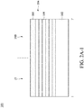
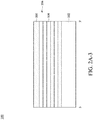
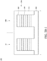
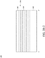
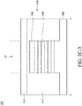
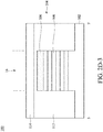
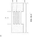
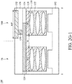
- FIGs. 2A-1 , 2A-2 , 2A-3 , 2B-1 , 2B-2 , 2B-3 , 2C-1 , 2C-2 , 2C-3 , 2D-1 , 2D-2 , 2D-3 , 2E-1 , 2E-2 , 2E-3 , 2F-1 , 2F-2 , 2F-3 , 2G-1 , 2G-2 , 2G-3 are cross-sectional representations of various stages of forming a nanosheet field effect transistor device structure 100 shown in FIG. 1 in accordance with some embodiments.
- FIGs. 2A-1 , 2B-1 , 2C-1 , 2D-1 , 2E-1 , 2F-1 , 2G-1 show cross-sectional representations taken along line 1-1' in FIG. 1 .
- FIGs. 2A-2 , 2B-2 , 2C-2 , 2D-2 , 2E-2 , 2F-2 , 2G-2 show cross-sectional representations taken along line 2-2' in FIG. 1 .
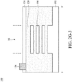
- FIGs. 2A-3 , 2B-3 , 2C-3 , 2D-3 , 2E-3 , 2F-3 , 2G-3 show cross-sectional representations taken along line 3-3' in FIG. 1 .
- the nanosheet field effect transistor device structure 100 includes a device region 10D and a boundary region 10B.
- the device region 10D includes gate structures 121 extending in the Y direction and a nanosheet stack 104 extending in the X direction.
- the nanosheet stack 104 in the device region 10D includes a channel region 16 under the gate structures 121 and a source/drain region 18 between the gate structures 121.
- the boundary region 10B includes a power rail 132 and another nanosheet stack 104 (not shown) extending in the X direction.
- the nanosheet stack 104 in the boundary region 10B is formed directly beneath the power rail 132 and electrically connected to the power rail 132.
- the source/drain region 18 is electrically connected to the power rail 132, as shown in FIG. 1 in accordance with some embodiments.
- the power rail resistance may be decreased.
- a substrate 102 is provided as shown in FIGs. 2A-1 , 2A-2 , and 2A-3 in accordance with some embodiments.
- the substrate 102 may be a semiconductor wafer such as a silicon wafer.
- the substrate 102 may also include other elementary semiconductor materials, compound semiconductor materials, and/or alloy semiconductor materials. Examples of the elementary semiconductor materials may include, but are not limited to, crystal silicon, polycrystalline silicon, amorphous silicon, germanium, and/or diamond.
- the compound semiconductor materials may include, but are not limited to, silicon carbide, gallium nitride, gallium arsenic, gallium phosphide, indium phosphide, indium arsenide, and/or indium antimonide.
- the alloy semiconductor materials may include, but are not limited to, SiGe, GaAsP, AlInAs, AlGaAs, GaInAs, GaInP, and/or GaInAsP.
- the substrate 102 includes an epitaxial layer.
- the substrate 102 has an epitaxial layer overlying a bulk semiconductor.
- the substrate 102 may also be semiconductor on insulator (SOI).
- the SOI substrate may be fabricated by a wafer bonding process, a silicon film transfer process, a separation by implantation of oxygen (SIMOX) process, other applicable methods, or a combination thereof.
- the substrate 102 may be an N-type substrate. In some embodiments, the substrate 102 may be a P-type substrate.
- a nanosheet stack 104 is formed on the substrate 102, as shown in FIGs. 1 , 2A-1 , 2A-2 , and 2A-3 in accordance with some embodiments.
- the nanosheet stack 104 may include first semiconductor layers 106 and second semiconductor layers 108 vertically alternately stacked over the substrate 102. It should be noted that, although there are four layers of the first semiconductor layers 106 and three layers of the second semiconductor layers 108 in the embodiments shown in FIGs. 2A-1 , 2A-2 , and 2A-3 , the number of first semiconductor layers 106 and the second semiconductor layers 108 is not limited thereto.
- the first semiconductor layers 106 may be made of silicon, silicon germanium, germanium tin, silicon germanium tin, gallium arsenide, indium gallium arsenide, indium arsenide, another suitable material, or a combination thereof.
- the semiconductor material layers 108 may be made of silicon, silicon germanium, germanium tin, silicon germanium tin, gallium arsenide, indium gallium arsenide, indium arsenide, another suitable material, or a combination thereof.
- the first semiconductor layers 106 and the second semiconductor material layers 108 are made of different materials.
- the first semiconductor layers 106 are made of silicon germanium
- the second semiconductor material layers 108 are made of silicon.
- the first semiconductor material layers 106 and the second semiconductor material layers 108 may be formed by an epitaxial growth process.
- Each of the first semiconductor material layers 106 and the second semiconductor material layers 108 may be formed by a selective epitaxial growth (SEG) process, a chemical vapor deposition (CVD) process (e.g., a vapor-phase epitaxy (VPE) process, a low-pressure CVD (LPCVD) process, and/or an ultra-high vacuum CVD (UHV-CVD) process), a molecular beam epitaxy process, another applicable process, or a combination thereof.
- SEG selective epitaxial growth
- CVD chemical vapor deposition
- VPE vapor-phase epitaxy
- LPCVD low-pressure CVD
- UHV-CVD ultra-high vacuum CVD
- a photoresist layer may be formed over the nanosheet stack 104 (not shown).
- the photoresist layer may be patterned by a patterning process including a photolithography process and an etching process.
- the photolithography process may include photoresist coating (e.g., spin-on coating), soft baking, mask aligning, exposure, post-exposure baking, developing the photoresist, rinsing and drying (e.g., hard baking).
- the etching process may include a dry etching process or a wet etching process.
- the nanosheet stack 104 and the upper portion of the substrate 102 are patterned by using the patterned photoresist layer as a mask as shown in FIGs. 2B-1 and 2B-3 in accordance with some embodiments.
- a patterned nanosheet stack 104 and a patterned substrate 102 may be obtained.
- the patterned photoresist layer may be removed.
- an isolation layer 110 is formed to cover the nanosheet stack 104 and the substrate 102, as shown in FIGs. 2B-1 and 2B-3 in accordance with some embodiments.
- the isolation layer 110 may be made of silicon oxide, silicon nitride, silicon oxynitride, fluoride-doped silicate glass (FSG), or another low-k dielectric material.
- the isolation layer 110 may be deposited by a deposition process, such as a chemical vapor deposition (CVD) process, a spin-on-glass process, or another applicable process.
- CVD chemical vapor deposition
- nanosheet stack 104 is patterned, separate nanosheet stacks 104 are formed in the source/drain region 18 in the device region 10D and the boundary region 10B respectively.
- the nanosheet stack 104 may be separated by the isolation layer 110.
- the isolation layer 110 is planarized to expose the top surface of the nanosheet stack 104 (not shown).
- the isolation layer 110 may be planarized by a chemical mechanical polishing (CMP) process.
- an etching process is performed on the isolation layer 110, as shown in FIGs. 2C-1 and 2C-3 in accordance with some embodiments.
- the isolation layer 110 is completely removed. Therefore, the nanosheet stack 104 and the substrate 102 are exposed, as shown in FIGs. 2C-1 .
- a portion of the isolation layer 110 is removed. As a result, the nanosheet stack 104 may be exposed and the remaining isolation layer 110 may surround the top portion of the substrate 102.
- the remaining isolation layer 110 may be an isolation structure such as a shallow trench isolation (STI) structure surrounding the top portion of the substrate 102.
- the isolation structure may be configured to prevent electrical interference or crosstalk.
- a dummy gate layer 112 is formed over the top surface and the sidewalls of the nanosheet stack 104 as shown in FIGs. 2C-2 and 2C-3 in accordance with some embodiments.
- the dummy gate layer 112 may define a channel region 16 and a source/drain region 18. As shown in FIG. 2C-2 in accordance with some embodiments, the channel region 16 is directly under the dummy gate layer 112, and the source/drain region 18 is on the opposite side of the channel region 16 and is not covered by the dummy gate layer 112.
- the dummy gate layer 112 may include a dummy dielectric layer and a dummy gate electrode layer (not shown).
- the dummy dielectric layer may be first conformally formed over the nanosheet stack 104.
- the dummy dielectric layer may be made of dielectric materials, such as silicon oxide, silicon nitride, silicon oxynitride, dielectric material(s) with high dielectric constant (high-k), or a combination thereof.
- the dummy dielectric layer may be formed by a deposition process, such as chemical vapor deposition (CVD), physical vapor deposition (PVD), atomic layer deposition (ALD), high density plasma CVD (HDPCVD), metal organic CVD (MOCVD), or plasma enhanced CVD (PECVD).
- CVD chemical vapor deposition
- PVD physical vapor deposition
- ALD atomic layer deposition
- HDPCVD high density plasma CVD
- MOCVD metal organic CVD
- PECVD plasma enhanced CVD
- the dummy gate electrode layer may be conformally formed over the dummy dielectric layer.
- the dummy gate electrode layer may be made of polysilicon.
- the dummy gate electrode layer may be formed by a deposition process, such as chemical vapor deposition (CVD), physical vapor deposition (PVD), atomic layer deposition (ALD), high density plasma CVD (HDPCVD), metal organic CVD (MOCVD), or plasma enhanced CVD (PECVD).
- CVD chemical vapor deposition
- PVD physical vapor deposition
- ALD atomic layer deposition
- HDPCVD high density plasma CVD
- MOCVD metal organic CVD
- PECVD plasma enhanced CVD
- an etching process is performed on the dummy gate layer 112 to form a dummy gate structure 112 by using a patterned hard mask layer 114.
- the dummy gate layer 112 may be partially removed in the etching process.
- the etching process may be a dry etching process or a wet etching process.
- the dummy dielectric layer and the dummy gate electrode layer are etched by a dry etching process.
- the dry etching process may include using a fluorine-based etchant gas, such as SF 6 , C x F y (where x and y may be positive integers), NF 3 , or a combination thereof.
- a fluorine-based etchant gas such as SF 6 , C x F y (where x and y may be positive integers), NF 3 , or a combination thereof.
- the first semiconductor layers 106 in the source/drain region 18 are removed, and a pair of spacers 116 are formed on sidewalls of the dummy gate layer 112, as shown in FIGs. 2D-1 and 2D-2 in accordance with some embodiments.
- the first semiconductor layers 106 in the source/drain region 18 may be removed by a dry etching process, such as an anisotropic etching process.
- the spacers 116 may be made of silicon oxide, silicon nitride, silicon oxynitride, and/or dielectric materials.
- the spacers 116 may be formed by a chemical vapor deposition (CVD) process, a spin-on-glass process, or other applicable processes. In some embodiments, the spacers 116 also fill in the gap between the first semiconductor layers 106 in the source/drain region 18 (not shown).
- epitaxial structures 118 are formed in the source/drain region 18 and the boundary region 10B, as shown in FIGs. 2E-1 and 2E-2 in accordance with some embodiments.
- the second semiconductor layers 108 in the source/drain region 18 are removed, and a strained material is grown by an epitaxial (epi) process to form the epitaxial structures 118 in the source/drain region 18 and the boundary region 10B.
- the lattice constant of the strained material may be different from the lattice constant of the substrate 102.
- the second semiconductor layers 108 in the source/drain region 18 are not removed, and the strained material is grown cladding around the second semiconductor layers 108 in the source/drain region 18 and the boundary region 10B.
- the type of the strained material in the present disclosure is not limited, depending on the needs of mobility or resistance improvement.
- the epitaxial structures 118 include vertically arranged epitaxial layers.
- the epitaxial structures 118 may include Ge, SiGe, InAs, InGaAs, InSb, GaAs, GaSb, InAlP, InP, SiC, SiP, other applicable materials, or a combination thereof.
- the epitaxial structures 118 may be formed by an epitaxial growth step, such as metalorganic chemical vapor deposition (MOCVD), metalorganic vapor phase epitaxy (MOVPE), plasma-enhanced chemical vapor deposition (PECVD), remote plasma-enhanced chemical vapor deposition (RP-CVD), molecular beam epitaxy (MBE), hydride vapor phase epitaxy (HVPE), liquid phase epitaxy (LPE), chloride vapor phase epitaxy (Cl-VPE), or any other suitable method.
- MOCVD metalorganic chemical vapor deposition
- MOVPE metalorganic vapor phase epitaxy
- PECVD plasma-enhanced chemical vapor deposition
- RP-CVD remote plasma-enh
- an inter-layer dielectric (ILD) structure 119 is formed to cover the epitaxial structure 118 as shown in FIGs. 2E-1 and 2E-2 in accordance with some embodiments.
- the inter-layer dielectric structure 119 may include multilayers made of multiple dielectric materials, such as silicon oxide, silicon nitride, silicon oxynitride, phosphosilicate glass (PSG), borophosphosilicate glass (BPSG), low-k dielectric material, and/or other applicable dielectric materials.
- low-k dielectric materials include, but are not limited to, fluorinated silica glass (FSG), carbon doped silicon oxide, amorphous fluorinated carbon, parylene, bis-benzocyclobutenes (BCB), or polyimide.
- FSG fluorinated silica glass
- carbon doped silicon oxide amorphous fluorinated carbon
- parylene parylene
- bis-benzocyclobutenes BCB
- polyimide polyimide
- the inter-layer dielectric structure 119 may be formed by chemical vapor deposition (CVD), spin-on coating, or other applicable processes.
- a planarizing process is performed on the inter-layer dielectric structure 119 until the top surface of the dummy gate layer 112 is exposed in accordance with some embodiments (not shown).
- the top surface of the dummy gate layer 112 may be substantially level with the top surfaces of the spacers 116 and the inter-layer dielectric structure 119.
- the planarizing process may include a grinding process, a chemical mechanical polishing (CMP) process, an etching process, another applicable process, or a combination thereof.
- the dummy gate layer 112 in the channel region 16 is removed, as shown in FIGs. 2E-2 and 2E-3 in accordance with some embodiments. Therefore, the first semiconductor layer 106 and the second semiconductor layer 108 in the channel region 16 may be exposed.
- the dummy gate layer 112 may be removed by an etching process, such as a dry etching process or a wet etching process.
- the first semiconductor 106 in the channel region 16 is removed, as shown in FIGs. 2E-2 and 2E-3 in accordance with some embodiments.
- the second semiconductor layers 108 are left in the channel region 16.
- the first semiconductor 106 in the channel region 16 may be removed by an etching process, such as an anisotropic etching process.
- a gate stack 120 is formed surrounding the second semiconductor layers 108 in the channel region 16, as shown in FIGs. 2E-2 and 2E-3 in accordance with some embodiments.
- the gate stack 120 fills in the space between the second semiconductor layers 108 in the channel region 16.
- the gate stack 120 may include a gate dielectric layer, a work function layer, and a gate electrode layer (not shown).
- the gate structure 121 in the channel region 16 includes vertically arranged second semiconductor layers 108 surrounded by the gate stack 120 as shown in FIGs. 2E-2 and 2E-3 in accordance with some embodiments.
- the gate dielectric layer may include a high-k dielectric layer (e.g., the dielectric constant is greater than 3.9) such as hafnium oxide (HfO 2 ).
- the high-k dielectric layer may include other high-k dielectrics such as LaO, AlO, ZrO, TiO, Ta 2 O 5 , Y 2 O 3 , SrTiO 3 , BaTiO 3 , BaZrO, HfZrO, HfLaO, HfTaO, HfSiO, HfSiON, HfTiO, LaSiO, AlSiO, BaTiO 3 , SrTiO 3 , Al 2 O 3 , other applicable high-k dielectric materials, or a combination thereof.
- the gate dielectric layer may be formed by a chemical vapor deposition process (CVD) (e.g., a plasma enhanced chemical vapor deposition (PECVD) process, a metalorganic chemical vapor deposition (MOCVD) process, or a high density plasma chemical vapor deposition (HDPCVD)), an atomic layer deposition (ALD) process (e.g., a plasma enhanced atomic layer deposition (PEALD) process), a physical vapor deposition (PVD) process (e.g., a vacuum evaporation process, or a sputtering process), other applicable processes, or a combination thereof.
- CVD chemical vapor deposition process
- PECVD plasma enhanced chemical vapor deposition
- MOCVD metalorganic chemical vapor deposition
- HDPCVD high density plasma chemical vapor deposition
- ALD atomic layer deposition
- PVD physical vapor deposition
- a vacuum evaporation process e.g., a vacuum evaporation process, or a
- the work function metal layer may be formed surrounding the gate dielectric layer.
- the work function metal layer may provide the desired work function for transistors to enhance device performance including improved threshold voltage.
- the work function metal layer may be made of metal materials, and the metal materials may include N-work-function metal or P-work-function metal.
- N-work-function metal may include tungsten (W), copper (Cu), titanium (Ti), silver (Ag), aluminum (Al), titanium aluminum alloy (TiAl), titanium aluminum nitride (TiAIN), tantalum carbide (TaC), tantalum carbon nitride (TaCN), tantalum silicon nitride (TaSiN), manganese (Mn), zirconium (Zr), or a combination thereof.
- the P-work-function metal may include titanium nitride (TiN), tungsten nitride (WN), tantalum nitride (TaN), ruthenium (Ru) or a combination thereof.
- the gate electrode layer is formed surrounding the work function metal layer.
- the gate electrode layer may be made of a conductive material, such as aluminum, copper, tungsten, titanium, tantulum, titanium nitride, tantalum nitride, nickel silicide, cobalt silicide, TaC, TaSiN, TaCN, TiAl, TiAIN, or other applicable materials.
- the gate electrode layer may be formed by a chemical vapor deposition process (e.g., a low pressure chemical vapor deposition process, or a plasma enhanced chemical vapor deposition process), a physical vapor deposition process (e.g., a vacuum evaporation process, or a sputtering process), other applicable processes, or a combination thereof.
- a first contact structure 122 is formed surrounding the epitaxial structure 118 in the source/drain region 18 and in the boundary region 10B, as shown in FIGs. 2F-1 and 2F-2 in accordance with some embodiments.
- the first contact structure 122 fills in the space between the vertically arranged epitaxial layers of the epitaxial structure 118. Therefore, the resistance of may be further reduced.
- openings are formed in the interlayer dielectric structure 119 (not shown), and a conductive material is filled in the openings to form the first contact structure 122.
- the first contact structure 122 may be made of metal materials (e.g., W, Al, or Cu), metal alloys, poly-Si, other applicable conductive materials, or a combination thereof.
- the first contact structure 122 may be formed by using a chemical vapor deposition process (CVD), a physical vapor deposition process (PVD, e.g., evaporation or sputter), an atomic layer deposition process (ALD), an electroplating process, another suitable process, or a combination thereof to deposit the conductive materials of the first contact structure 122 in the openings.
- a chemical mechanical polishing (CMP) process or an etching back process may be then optionally performed to remove excess conductive materials to form the first contact structure 122.
- a dielectric layer 124 is formed over the ILD structure 119 and a metal layer 126 is formed in the dielectric layer 124, as shown in FIGs. 2G-1 and 2G-2 in accordance with some embodiments.
- the metal layer 126 is in direct contact with and electrically connected to the first contact structure 122 formed in the source/drain region 18 and in the boundary region 10B.
- the dielectric layer 124 may be made of silicon oxide.
- the dielectric layer 124 may be deposited by CVD processes such as atmospheric pressure CVD (APCVD), low-pressure CVD (LPCVD), and plasma-enhanced CVD (PECVD).
- the metal layer 126 may include Cu, W, Ag, Ag, Sn, Ni, Co, Cr, Ti, Pb, Au, Bi, Sb, Zn, Zr, Mg, In, Te, Ga, other applicable metallic materials, an alloy thereof, or a combination thereof.
- the metal layer 126 includes a stacked structure of TiN/AlCu/TiN.
- the metal layer 126 may be deposited by a physical vapor deposition process (e.g., evaporation or sputtering), an atomic layer deposition process (ALD), an electroplating process, other applicable processes or a combination thereof, and then a chemical mechanical polishing (CMP) process or an etching back process is then optionally performed to remove excess conductive materials.
- a physical vapor deposition process e.g., evaporation or sputtering
- ALD atomic layer deposition process
- electroplating process other applicable processes or a combination thereof
- CMP chemical mechanical polishing
- a dielectric layer 128 is formed over the dielectric layer 124, and a via 130 and a power rail 132 are formed in the dielectric layer 128 in the boundary region 10B, as shown in FIG. 2G-1 in accordance with some embodiments.
- the power rail 132 is formed directly above the epitaxial structure 118 in the boundary region 10B and electrically connected to the epitaxial structure 118 in the boundary region 10B.
- the processes for forming the via 130 may be the same as, or similar to, those used to form the first contact structure 122.
- the processes for forming the power rail 132 may be the same as, or similar to, those used to form the metal layer 126. For the purpose of brevity, the descriptions of these processes are not repeated herein.
- the via 130 and the power rail 132 are formed separately.
- the via 130 and the power rail 132 are formed at the same time by a dual damascene process.
- a second contact structure 134 is formed on the gate stack 120, as shown in FIG. 2G-3 in accordance with some embodiments.
- the second contact structure 134 is electrically connected to the gate stack 120.
- the processes for forming the second contact structure 134 are the same as, or similar to, those used to form the first contact structure 122. For the purpose of brevity, the descriptions of these processes are not repeated herein.
- the space S between the epitaxial structure 118 in the source/drain region 18 and the epitaxial structure 118 in the boundary region 10B is in a range from about 5% to about 100% of the width W1 of the epitaxial structure 118 in the source/drain region 18. In some other preferred embodiments as shown in FIG. 2G-1 , the space S between the epitaxial structure 118 in the source/drain region 18 and the epitaxial structure 118 in the boundary region 10B is in a range from about 10% to about 70% of the width W1 of the epitaxial structure 118 in the source/drain region 18. If the space S is too large, the circuit area may be too large. If the space S is too small, the epitaxial structure 118 in the source/drain region 18 and the epitaxial structure 118 in the boundary region 10B may short-circuit and there may be more defects.
- the width W2 of the epitaxial structure 118 in the boundary region 10B is in a range from about 10% to about 150% of the width WP of the power rail 132. In some other preferred embodiments as shown in FIG. 2G-1 , the width W2 of the epitaxial structure 118 in the boundary region 10B is in a range from about 25% to about 100% of the width WP of the power rail 132. If the width W2 is too wide, the epitaxial structure 118 in the source/drain region 18 and the epitaxial structure 118 in the boundary region 10B may short-circuit. If the width W2 is to narrow, the power rail resistance may still be high.
- the power rail resistance may be effectively reduced, the IR drop may be suppressed, and the electron migration may be improved. Moreover, with the first contact structure 122 filled in the space between the vertically arranged epitaxial layers 118, the power rail resistance may be further reduced.
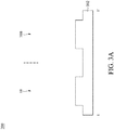
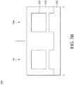
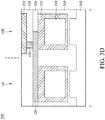
- FIGs. 3A-3D are cross-sectional representations of various stages of forming a nanosheet field effect transistor device structure 200, in accordance with some other embodiments of the disclosure. Some processes or devices are the same as, or similar to, those described in the embodiments above, and therefore the descriptions of these processes and devices are not repeated herein. The difference from the embodiments described above is that, as shown in FIGs. 3B-3D in accordance with some embodiments, the epitaxial structures 218 in the source/drain region 18 and the boundary region 10B are single epitaxial blocks.
- the first semiconductor layers 106 and the second semiconductor layers 108 in the source/drain region 18 and the boundary region 10B are both removed by an etching process, as shown in FIG. 3A in accordance with some embodiments.
- the etching process may include dry etching process, wet etching process, reactive ion etching, and/or other suitable etching process.
- the dry etching process may be performed by an oxygen-containing gas, a fluorine-containing gas (such as CF 4 , SF 6 , CH 2 F 2 , CHF 3 , and/or C 2 F 6 ), a chlorine-containing gas (such as Cl 2 , CHCl 3 , CCl 4 , and/or BCl 3 ), bromine-containing gas (such as HBr and/or CHBR 3 ), iodine- containing gas, other suitable gas and/or plasma, or a combination thereof.
- a fluorine-containing gas such as CF 4 , SF 6 , CH 2 F 2 , CHF 3 , and/or C 2 F 6
- a chlorine-containing gas such as Cl 2 , CHCl 3 , CCl 4 , and/or BCl 3
- bromine-containing gas such as HBr and/or CHBR 3
- iodine- containing gas other suitable gas and/or plasma, or a combination thereof.
- the wet etching process may be performed in wet etching etchant including diluted hydrofluoric acid (DHF), potassium hydroxide (KOH), ammonia, hydrofluoric acid (HF), nitric acid (HNO 3 ), and/or acetic acid (CH 3 COOH), other suitable wet etching etchant, or a combination thereof.
- wet etching etchant including diluted hydrofluoric acid (DHF), potassium hydroxide (KOH), ammonia, hydrofluoric acid (HF), nitric acid (HNO 3 ), and/or acetic acid (CH 3 COOH), other suitable wet etching etchant, or a combination thereof.
- an epitaxial structure 218 which is a single epitaxial block is formed in the source/drain region 18 and the boundary region 10B, as shown in FIG. 3B in accordance with some embodiments.
- the processes of forming the epitaxial structure 218 are the same as, or similar to, those used to form the epitaxial structure 118 described in the previous embodiments. For the purpose of brevity, the descriptions of these processes are not repeated herein.
- the first contact structure 122 is formed surrounding the epitaxial structure 218 in the source/drain region 18 and the boundary region 10B, as shown in FIG. 3C in accordance with some embodiments.
- the epitaxial structure 218 is spaced apart from the substrate as shown in FIG. 3C , and first contact structure 122 wrap around the epitaxial structure 218 to further reduce the resistance. This may improve production yield and transistor current by mobility enhancement.
- the power rail 132 is formed directly above the epitaxial structure 218 formed in the boundary region 10B, and the power rail 132 is electrically connected to the epitaxial structure 218 formed in the boundary region 10B, as shown in FIG. 3D in accordance with some embodiments.
- the power rail resistance may be effectively reduced, the IR drop may be suppressed, and the electron migration may be improved.
- the epitaxial structure 218 is a single epitaxial block, it may be easier to wrap around the first contact structure 122, and the production yield may be further improved and transistor current by mobility enhancement.
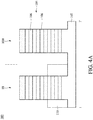
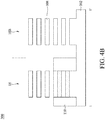
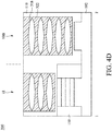
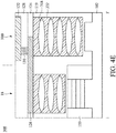
- FIGs. 4A-4E are cross-sectional representations of various stages of a modified nanosheet field effect transistor device structure 300, in accordance with some other embodiments of the disclosure. Some processes or devices are the same as, or similar to, those described in the embodiments above, and therefore the descriptions of these processes and devices are not repeated herein. The difference from the embodiments described above is that, as shown in FIG. 4E in accordance with some embodiments, the epitaxial structure 318 in the source/drain region 18 and the epitaxial structure 318 in the boundary region 10B include a different number of epitaxial layers.
- the number of first semiconductor layers 106 and the second semiconductor layers 108 in the source/drain region 18 and in the boundary region 10B exposed from the isolation layer 110 are different, as shown in FIG. 4A in accordance with some embodiments.
- the number of first semiconductor layers 106 and the second semiconductor layers 108 in the boundary region 10B is more than that of in the source/drain region 18. Therefore, after removing the first semiconductor layers 106 exposed from the isolation layer 110, the number of left second semiconductor layers 108 in the source/drain region 18 and in the boundary region 10B exposed from the isolation layer 110 are different, as shown in FIG. 4B in accordance with some embodiments.
- the epitaxial structure 318 is formed at where the second semiconductor layers 108 are exposed from the isolation layer 110, as shown in FIGs. 4C in accordance with some embodiments.
- the number of the epitaxial layers of the epitaxial structure 318 in the source/drain region 18 and in the boundary region 10B may be different.
- the contact structure 322 wrapping around the epitaxial structure 318 in the boundary region 10B is larger than that of in the source/drain region 18. Therefore, the resistance of the contact structure 322 in the boundary region 10B is lower than that in the source/drain region 18.
- the number of epitaxial layers of the epitaxial structure 318 in the source/drain region 18 and in the boundary region 10B is not limited thereto.
- the power rail resistance may be effectively reduced, the IR drop may be suppressed, and the electron migration may be improved. Moreover, since the epitaxial structure 318 is larger under the power rail 132, the power rail resistance may be further reduced.
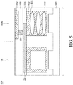
- FIG. 5 is a cross-sectional representation of a modified nanosheet field effect transistor device structure 400, in accordance with some other embodiments of the disclosure. Some processes or devices are the same as, or similar to, those described in the embodiments above, and therefore the descriptions of these processes and devices are not repeated herein. The difference from the embodiments described above is that, as shown in FIG. 5 in accordance with some embodiments, the epitaxial structure 418 in the source/drain region 18 includes a single epitaxial block, and the epitaxial structure 418 in the boundary region 10B includes vertically arranged epitaxial layers.
- the first semiconductor layers 106 and the second semiconductor layers 108 in the source/drain region 18 are removed by an etching process, as shown in FIG. 5 in accordance with some embodiments. Meanwhile, only the first semiconductor layers 106 in the boundary region 10B are removed by the etching process. Therefore, a single epitaxial block may be formed in the source/drain region 18 and vertically arranged epitaxial layers may be formed in the boundary region 10B. Since in the boundary region 10B the epitaxial layers 418 are vertically arranged, the first contact structure 422 filled in the space between the vertically arranged epitaxial layers 418. The contact structure 422 may have a lower resistance in the boundary region 10B than in the source/drain region 18, and the power rail resistance may be further reduced.
- the power rail resistance may be effectively reduced, the IR drop may be suppressed, and the electron migration may be improved. Since the epitaxial structure 418 in the source/drain region 18 is a single epitaxial block, it may be easier to wrap around the first contact structure 422, and the production yield may be further improved and transistor current by mobility enhancement. Moreover, since the epitaxial structure 418 in the boundary region 10B is vertically arranged epitaxial layers, the power rail resistance may be further reduced.
- FIG. 6 is a perspective representation of a modified nanosheet field effect transistor device structure 500 in accordance with some further embodiments.
- FIG. 7 is a top view of a modified nanosheet field effect transistor device structure 500 in accordance with some further embodiments.
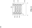
- FIG. 8 is a cross-sectional representation of a modified nanosheet field effect transistor device structure 500 in accordance with some further embodiments.
- FIG. 8 shows a cross-sectional representation taken along line 8-8' in FIG. 7 .
- a pair of contact structures 522 are disposed on opposite sides of the epitaxial structure 518. Moreover, each of the contact structures 522 surrounds a portion of the epitaxial structure 518, and the pair of contact structures 522 are spaced apart from each other by the epitaxial structure 518.
- the contact structures 522 are formed on opposite sides of the epitaxial structure 518, as shown in FIGs. 6-8 in accordance with some embodiments. Therefore, a resistor 536 is formed at the epitaxial structure 518 between the contact structures 522. Compared to the conventional resistor design, the resistor 536 between the contact structures 522 may be formed without extra masks and the chip area may be reduced.
- another resistor 536P is formed between the contact structures 522P.
- the contact structures 522 are electrically connected to the contact structures 522P at each end. Therefore, the resistors 536 and 536P between the contact structures 522 and 522P are connected in parallel.
- gate structures 121 and 121P and two pair of contact structures 522 and 522P in the embodiments shown in FIGs. 6 and 7 , the number of gate structures 121 and 121P and contact structures 522 and 522P is not limited thereto. The number of gate structures 121 and 121P and contact structures 522 and 522P may be modified, depending on the demands on the resistance of the resistor.
- the ratio of width W to height H of the epitaxial structure 518 is in a range from about 100% to about 1000%. If the ratio is too high, it may not be easy to form an epitaxial structure 518 between the gate structures 121. If the ratio is too low, extra chip area may be needed to meet the resistance requirements.
- the width W of the epitaxial structure 518 may be modified, depending on the demands on the resistance of the resistor 536.
- the epitaxial structure 518 may include vertically arranged epitaxial layers as shown in FIG. 8 in accordance with some embodiments. Therefore, the resistance of the resistor 536 is the parallel resistance of each epitaxial layer is connected in parallel between the contact structures 522.By forming epitaxial structure 518 between a pair of contact structures 522 and 522P, a resistor 536 is formed without using an extra mask. The resistance of the resistor 536 may be modified by changing the width W of the epitaxial structure 518 and the number of epitaxial structures 518 connected in parallel.
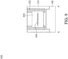
- FIG. 9 is a cross-sectional representation of a modified nanosheet field effect transistor device structure 600 in accordance with some further embodiments. Some processes or devices are the same as, or similar to, those described in the embodiments above, and therefore the descriptions of these processes and devices are not repeated herein. The difference from the embodiments described above is that, as shown in FIG. 9 in accordance with some embodiments, the epitaxial structure 618 includes a single epitaxial block.
- the epitaxial structure 618 is formed by removing the first semiconductor layers 106 and the second semiconductor layers 108 between the gate structures 121 by an etching process and forming a single epitaxial block between the gate structures 121. Therefore, it may be easier to form the epitaxial structure 618, and the production yield may be further improved and transistor current by mobility enhancement.
- a resistor 636 is formed without using an extra mask.
- the resistance of the resistor 636 may be modified by adjusting the width W of the epitaxial structure 618 and the number of epitaxial structures 618 connected in parallel.
- the epitaxial structure 618 since the epitaxial structure 618 includes a single epitaxial block, it may be easier to be formed the epitaxial structure 618, and the production yield may be further improved and transistor current by mobility enhancement.
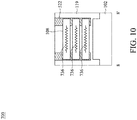
- FIG. 10 is a cross-sectional representation of a modified nanosheet field effect transistor device structure 700 in accordance with some further embodiments. Some processes or devices are the same as, or similar to, those described in the embodiments above, and therefore the descriptions of these processes and devices are not repeated herein. The difference from the embodiments described above is that, as shown in FIG. 10 in accordance with some embodiments, the epitaxial structure is not formed and the second semiconductor layers 108 are left between the gate structures as the body of resistor 736.
- a resistor 736 is formed without using an extra mask.
- the resistance of the resistor 736 may be modified by adjusting the width W of the second semiconductor layers 108 and the number of second semiconductor layers 108 connected in parallel.
- by taking the second semiconductor layers 108 is as the body of the resistor 736, it may save the production cost and time.
- a method of forming a nanosheet field effect transistor device structure is provided.
- the power rail resistance may be reduced, the IR drop may be suppressed, and the electron migration may be improved.
- the power rail resistance may be further reduced.
- the production yield may be improved and transistor current by mobility enhancement.
- a resistor may be formed without using an extra mask. The resistance of the resistor may be fine-tuned by modifying the dimensions of the epitaxial structure, or connecting the same epitaxial structures in parallel.
Landscapes
- Engineering & Computer Science (AREA)
- Chemical & Material Sciences (AREA)
- Nanotechnology (AREA)
- Physics & Mathematics (AREA)
- Mathematical Physics (AREA)
- Theoretical Computer Science (AREA)
- Crystallography & Structural Chemistry (AREA)
- Insulated Gate Type Field-Effect Transistor (AREA)
- Thin Film Transistor (AREA)
- Chemical Kinetics & Catalysis (AREA)
- General Chemical & Material Sciences (AREA)
- Electrodes Of Semiconductors (AREA)
Abstract
Description
- The disclosure relates to a semiconductor structure, and more particularly to a nanosheet field effect transistor device structure and a method for forming a nanosheet field effect transistor device structure.
- The semiconductor integrated circuit industry has experienced rapid growth. The development of integrated-circuit design and advancements in materials technology has produced generations of integrated circuits. Each generation has smaller and more complex circuits than the previous generation. In the process of integrated-circuit development, geometric size has gradually been reduced.
- The gate-all around (GAA) nanosheet (NS) device has been introduced in an effort to improve gate control by increasing gate and channel coupling, reduce OFF-state leakage current, and reduce short-channel effects (SCE). A gate-all around nanosheet device has a gate stack wrapped around the channel region providing access to the channel on four sides. The gate-all around nanosheet device provides a channel in a silicon nanosheet.
- As integrated circuits have shrunk, the size of the transistor and metal lines has decreased. Therefore, the power rail resistance may increase, and the IR drop may lead to poor circuit performance and worse electron migration (EM). Moreover, a conventional Hi-R resistor incurs an extra cost for the mask and takes up more chip area.
- Although existing nanosheet field effect transistor device structures have generally been adequate for their intended purposes, they have not been entirely satisfactory in all respects, and need to be improved. This is especially true of the control of the power rail resistance and a resistor with lower cost.
- The present disclosure provides a nanosheet field effect transistor device structure, including a gate structure, first epitaxial structures, a power rail, and a second epitaxial structure. The gate structure is disposed on a substrate extending in a first direction. The first epitaxial structures are surrounded by a contact structure disposed on opposite sides of the gate structure extending in the first direction. The power rail is spaced apart from the gate structure and the first epitaxial structures. The power rail extends in the second direction, which is perpendicular to the first direction. The second epitaxial structure surrounded by the contact structure disposed directly beneath the power rail. The second epitaxial structure is electrically connected to the power rail.
- The first epitaxial structures or the second epitaxial structure may comprise a plurality of vertically arranged epitaxial layers.
- The first epitaxial structures and the second epitaxial structure may comprise a different number of epitaxial layers.
- The first epitaxial structures and the second epitaxial structure may comprise a same number of epitaxial layers.
- The first epitaxial structures or the second epitaxial structure may comprise a single epitaxial block.
- The gate structure may comprise a plurality of vertically arranged second semiconductor layers surrounded by a gate stack.
- A space between the first epitaxial structures and the second epitaxial structure may be in a range from about 10% to about 70% of a width of the first epitaxial structures.
- A width of the second epitaxial structure may be in a range from about 25% to about 100% of a width of the power rail.
- The present disclosure also provides a method for forming a nanosheet field effect transistor device structure. The method includes forming a nanosheet stack comprising vertically alternately stacked first semiconductor layers and second semiconductor layers on a substrate. The substrate includes a device region and a boundary region. The device region includes a channel region and a source/drain region. The method also includes removing the nanosheet stack and forming epitaxial structures in the source/drain region and the boundary region. The method also includes removing the first semiconductor layers of the nanosheet stack in the channel region and forming a gate stack surrounding the second semiconductor layers. The method also includes forming a contact structure surrounding the epitaxial structures in the source/drain region and the boundary region. The method also includes forming a power rail in the boundary region directly above the epitaxial structure in the boundary region. The power rail is electrically connected to the epitaxial structure in the boundary region. The epitaxial structures in the source/drain region and the epitaxial structures in the boundary region are spaced apart from each other.
- Forming the epitaxial structures in the source/drain region or the boundary region may comprise forming a plurality of vertically arranged epitaxial layers.
- Forming the epitaxial structures in the source/drain region or the boundary region may comprise forming a single epitaxial block.
- The method may further comprise forming a dummy gate covering the nanosheet stack in the channel region before forming the epitaxial structures in the source/drain region and the boundary region.
- The method may further comprise forming a spacer layer on the sidewalls of the dummy gate before removing the nanosheet stack in the source/drain region and the boundary region.
- The method may further comprise removing the dummy gate in the channel region before removing the first semiconductor layers of the nanosheet stack in the channel region.
- The first semiconductor layers and second semiconductor layers may be made of different materials.
- The present disclosure further provides a nanosheet field effect transistor device structure, including first gate structures, a first epitaxial structure, and a pair of first contact structures. The first gate structures are disposed on a substrate. The first epitaxial structure is disposed between the first gate structures. The pair of first contact structures are disposed on opposite sides of the first epitaxial structure. The pair of first contact structures surround a portion of the first epitaxial structure, and the pair of first contact structures are spaced apart from each other by the first epitaxial structure.
- The first epitaxial structure may comprise a plurality of vertically arranged epitaxial layers.
- The first epitaxial structure may comprise a single epitaxial block.
- The ratio of a width and a height of the first epitaxial structure may be in a range from about 100% to about 1000%.
- The semiconductor device structure may further comprise a second gate structure disposed parallel to the first gate structures; a second epitaxial structure disposed between the second gate structure and the first gate structures; and a pair of second contact structures disposed on opposite sides of the second epitaxial structure, wherein the pair of second contact structures surround a portion of the second epitaxial structure, and the pair of second contact structures are spaced apart from each other by the second epitaxial structure.
- The first and second contact structures disposed on an end of the first epitaxial structure and the second epitaxial structure may be electrically connected to each other, and the first and second contact structures disposed on another end of first epitaxial structure and the second epitaxial structure may be electrically connected to each other.
- A detailed description is given in the following embodiments with reference to the accompanying drawings.
- Aspects of the present disclosure are best understood from the following detailed description when read with the accompanying figures. It should be noted that, in accordance with the standard practice in the industry, various features are not drawn to scale. In fact, the dimensions of the various features may be arbitrarily increased or reduced for clarity of discussion.
-
FIG. 1 is a top view of a nanosheet field effect transistor device structure in accordance with some embodiments. -
FIGs. 2A-1 ,2A-2 ,2A-3 ,2B-1 ,2B-2 ,2B-3 ,2C-1 ,2C-2 ,2C-3 ,2D-1 ,2D-2 ,2D-3 ,2E-1 ,2E-2 ,2E-3 ,2F-1 ,2F-2 ,2F-3 ,2G-1 ,2G-2 ,2G-3 are cross-sectional representations of various stages of forming a nanosheet field effect transistor device structure in accordance with some embodiments. -
FIGs. 3A-3D are cross-sectional representations of various stages of forming a nanosheet field effect transistor device structure in accordance with some other embodiments. -
FIGs. 4A-4E are cross-sectional representations of various stages of forming a nanosheet field effect transistor device structure in accordance with some other embodiments. -
FIG. 5 is a cross-sectional representation of a nanosheet field effect transistor device structure in accordance with some other embodiments. -
FIG. 6 is a perspective representation of a nanosheet field effect transistor device structure in accordance with some further embodiments. -
FIG. 7 is a top view of a nanosheet field effect transistor device structure in accordance with some further embodiments. -
FIG. 8 is a cross-sectional representation of a nanosheet field effect transistor device structure in accordance with some further embodiments. -
FIG. 9 is a cross-sectional representation of a nanosheet field effect transistor device structure in accordance with some other embodiments. -
FIG. 10 is a cross-sectional representation of a nanosheet field effect transistor device structure in accordance with some other embodiments. - The following disclosure provides many different embodiments, or examples, for implementing different features of the disclosure. Specific examples of components and arrangements are described below to simplify the present disclosure. These are, of course, merely examples and are not intended to be limiting. For example, the formation of a first feature over or on a second feature in the description that follows may include embodiments in which the first and second features are formed in direct contact, and may also include embodiments in which additional features may be formed between the first and second features, such that the first and second features may not be in direct contact. In addition, the present disclosure may repeat reference numerals and/or letters in the various examples. This repetition is for the purpose of simplicity and clarity and does not in itself dictate a relationship between the various embodiments and/or configurations discussed.
- Furthermore, spatially relative terms, such as "beneath," "below," "lower," "above," "upper" and the like, may be used herein for ease of description to describe one element or feature's relationship to other elements or features as illustrated in the figures. The spatially relative terms are intended to encompass different orientations of the device in use or operation in addition to the orientation depicted in the figures. The apparatus may be otherwise oriented (rotated 90 degrees or at other orientations) and the spatially relative descriptors used herein may likewise be interpreted accordingly.
- Herein, the terms "around," "about," "substantial" usually mean within 20% of a given value or range, preferably within 10%, and better within 5%, or 3%, or 2%, or 1%, or 0.5%. It should be noted that the quantity herein is a substantial quantity, which means that the meaning of "around," "about," "substantial" are still implied even without specific mention of the terms "around," "about," "substantial."
- Although some embodiments are discussed with operations performed in a particular order, these operations may be performed in another logical order. In different embodiments, additional operations can be provided before, during, and/or after the stages described the present disclosure. Some of the stages that are described can be replaced or eliminated for different embodiments. Additional features can be added to the semiconductor structure in the present disclosure. Some of the features described below can be replaced or eliminated for different embodiments.
- The embodiments of the present disclosure provide a nanosheet field effect transistor device structure. By forming an epitaxial structure under the power rail and electrically connected to the power rail, the power rail resistance may be reduced and the circuit performance may be enhanced and the electron migration (EM) may be mitigated. Moreover, by forming contact structures on opposite sides of the epitaxial structures, a resistor producing in the front-end process is provided. The chip area and the cost for the mask may be further reduced.
-
FIG. 1 is a top view of a nanosheet field effecttransistor device structure 100 in accordance with some embodiments.FIGs. 2A-1 ,2A-2 ,2A-3 ,2B-1 ,2B-2 ,2B-3 ,2C-1 ,2C-2 ,2C-3 ,2D-1 ,2D-2 ,2D-3 ,2E-1 ,2E-2 ,2E-3 ,2F-1 ,2F-2 ,2F-3 ,2G-1 ,2G-2 ,2G-3 are cross-sectional representations of various stages of forming a nanosheet field effecttransistor device structure 100 shown inFIG. 1 in accordance with some embodiments.FIGs. 2A-1 ,2B-1 ,2C-1 ,2D-1 ,2E-1 ,2F-1 ,2G-1 show cross-sectional representations taken along line 1-1' inFIG. 1 .FIGs. 2A-2 ,2B-2 ,2C-2 ,2D-2 ,2E-2 ,2F-2 ,2G-2 show cross-sectional representations taken along line 2-2' inFIG. 1 .FIGs. 2A-3 ,2B-3 ,2C-3 ,2D-3 ,2E-3 ,2F-3 ,2G-3 show cross-sectional representations taken along line 3-3' inFIG. 1 . - As shown in
FIG. 1 in accordance with some embodiments, the nanosheet field effecttransistor device structure 100 includes adevice region 10D and aboundary region 10B. Thedevice region 10D includesgate structures 121 extending in the Y direction and ananosheet stack 104 extending in the X direction. Thenanosheet stack 104 in thedevice region 10D includes achannel region 16 under thegate structures 121 and a source/drain region 18 between thegate structures 121. Theboundary region 10B includes apower rail 132 and another nanosheet stack 104 (not shown) extending in the X direction. Thenanosheet stack 104 in theboundary region 10B is formed directly beneath thepower rail 132 and electrically connected to thepower rail 132. The source/drain region 18 is electrically connected to thepower rail 132, as shown inFIG. 1 in accordance with some embodiments. By forming ananosheet stack 104 in theboundary region 10B is formed directly beneath thepower rail 132 and electrically connected to thepower rail 132, the power rail resistance may be decreased. - The following description describes the forming method of the nanosheet field effect
transistor device structure 100 inFIG. 1 . Asubstrate 102 is provided as shown inFIGs. 2A-1 ,2A-2 , and2A-3 in accordance with some embodiments. Thesubstrate 102 may be a semiconductor wafer such as a silicon wafer. Thesubstrate 102 may also include other elementary semiconductor materials, compound semiconductor materials, and/or alloy semiconductor materials. Examples of the elementary semiconductor materials may include, but are not limited to, crystal silicon, polycrystalline silicon, amorphous silicon, germanium, and/or diamond. Examples of the compound semiconductor materials may include, but are not limited to, silicon carbide, gallium nitride, gallium arsenic, gallium phosphide, indium phosphide, indium arsenide, and/or indium antimonide. Examples of the alloy semiconductor materials may include, but are not limited to, SiGe, GaAsP, AlInAs, AlGaAs, GaInAs, GaInP, and/or GaInAsP. In some embodiments, thesubstrate 102 includes an epitaxial layer. For example, thesubstrate 102 has an epitaxial layer overlying a bulk semiconductor. In addition, thesubstrate 102 may also be semiconductor on insulator (SOI). The SOI substrate may be fabricated by a wafer bonding process, a silicon film transfer process, a separation by implantation of oxygen (SIMOX) process, other applicable methods, or a combination thereof. In some embodiments, thesubstrate 102 may be an N-type substrate. In some embodiments, thesubstrate 102 may be a P-type substrate. - Next, a
nanosheet stack 104 is formed on thesubstrate 102, as shown inFIGs. 1 ,2A-1 ,2A-2 , and2A-3 in accordance with some embodiments. Thenanosheet stack 104 may include first semiconductor layers 106 and second semiconductor layers 108 vertically alternately stacked over thesubstrate 102. It should be noted that, although there are four layers of the first semiconductor layers 106 and three layers of the second semiconductor layers 108 in the embodiments shown inFIGs. 2A-1 ,2A-2 , and2A-3 , the number of first semiconductor layers 106 and the second semiconductor layers 108 is not limited thereto. - The first semiconductor layers 106 may be made of silicon, silicon germanium, germanium tin, silicon germanium tin, gallium arsenide, indium gallium arsenide, indium arsenide, another suitable material, or a combination thereof. The semiconductor material layers 108 may be made of silicon, silicon germanium, germanium tin, silicon germanium tin, gallium arsenide, indium gallium arsenide, indium arsenide, another suitable material, or a combination thereof. In some embodiments, the first semiconductor layers 106 and the second semiconductor material layers 108 are made of different materials. For example, the first semiconductor layers 106 are made of silicon germanium, and the second semiconductor material layers 108 are made of silicon.
- The first semiconductor material layers 106 and the second semiconductor material layers 108 may be formed by an epitaxial growth process. Each of the first semiconductor material layers 106 and the second semiconductor material layers 108 may be formed by a selective epitaxial growth (SEG) process, a chemical vapor deposition (CVD) process (e.g., a vapor-phase epitaxy (VPE) process, a low-pressure CVD (LPCVD) process, and/or an ultra-high vacuum CVD (UHV-CVD) process), a molecular beam epitaxy process, another applicable process, or a combination thereof.
- Afterwards, a photoresist layer may be formed over the nanosheet stack 104 (not shown). The photoresist layer may be patterned by a patterning process including a photolithography process and an etching process. The photolithography process may include photoresist coating (e.g., spin-on coating), soft baking, mask aligning, exposure, post-exposure baking, developing the photoresist, rinsing and drying (e.g., hard baking). The etching process may include a dry etching process or a wet etching process.
- Next, after the photoresist layer is patterned, the
nanosheet stack 104 and the upper portion of thesubstrate 102 are patterned by using the patterned photoresist layer as a mask as shown inFIGs. 2B-1 and2B-3 in accordance with some embodiments. As a result, apatterned nanosheet stack 104 and apatterned substrate 102 may be obtained. Afterwards, the patterned photoresist layer may be removed. - Next, an
isolation layer 110 is formed to cover thenanosheet stack 104 and thesubstrate 102, as shown inFIGs. 2B-1 and2B-3 in accordance with some embodiments. Theisolation layer 110 may be made of silicon oxide, silicon nitride, silicon oxynitride, fluoride-doped silicate glass (FSG), or another low-k dielectric material. Theisolation layer 110 may be deposited by a deposition process, such as a chemical vapor deposition (CVD) process, a spin-on-glass process, or another applicable process. - As shown in
FIGs. 1 and2B-1 in accordance with some embodiments, after thenanosheet stack 104 is patterned,separate nanosheet stacks 104 are formed in the source/drain region 18 in thedevice region 10D and theboundary region 10B respectively. Thenanosheet stack 104 may be separated by theisolation layer 110. - Afterwards, in some embodiments, the
isolation layer 110 is planarized to expose the top surface of the nanosheet stack 104 (not shown). In some embodiments, theisolation layer 110 may be planarized by a chemical mechanical polishing (CMP) process. - Next, an etching process is performed on the
isolation layer 110, as shown inFIGs. 2C-1 and2C-3 in accordance with some embodiments. In some embodiments, theisolation layer 110 is completely removed. Therefore, thenanosheet stack 104 and thesubstrate 102 are exposed, as shown inFIGs. 2C-1 . In some embodiments, a portion of theisolation layer 110 is removed. As a result, thenanosheet stack 104 may be exposed and the remainingisolation layer 110 may surround the top portion of thesubstrate 102. The remainingisolation layer 110 may be an isolation structure such as a shallow trench isolation (STI) structure surrounding the top portion of thesubstrate 102. The isolation structure may be configured to prevent electrical interference or crosstalk. - Afterwards, a
dummy gate layer 112 is formed over the top surface and the sidewalls of thenanosheet stack 104 as shown inFIGs. 2C-2 and2C-3 in accordance with some embodiments. Thedummy gate layer 112 may define achannel region 16 and a source/drain region 18. As shown inFIG. 2C-2 in accordance with some embodiments, thechannel region 16 is directly under thedummy gate layer 112, and the source/drain region 18 is on the opposite side of thechannel region 16 and is not covered by thedummy gate layer 112. - The
dummy gate layer 112 may include a dummy dielectric layer and a dummy gate electrode layer (not shown). The dummy dielectric layer may be first conformally formed over thenanosheet stack 104. The dummy dielectric layer may be made of dielectric materials, such as silicon oxide, silicon nitride, silicon oxynitride, dielectric material(s) with high dielectric constant (high-k), or a combination thereof. The dummy dielectric layer may be formed by a deposition process, such as chemical vapor deposition (CVD), physical vapor deposition (PVD), atomic layer deposition (ALD), high density plasma CVD (HDPCVD), metal organic CVD (MOCVD), or plasma enhanced CVD (PECVD). - After forming the dummy dielectric layer, the dummy gate electrode layer may be conformally formed over the dummy dielectric layer. The dummy gate electrode layer may be made of polysilicon. The dummy gate electrode layer may be formed by a deposition process, such as chemical vapor deposition (CVD), physical vapor deposition (PVD), atomic layer deposition (ALD), high density plasma CVD (HDPCVD), metal organic CVD (MOCVD), or plasma enhanced CVD (PECVD).
- Afterwards, as shown in
FIGs. 2C-1 ,2C-2 and2C-3 in accordance with some embodiments, an etching process is performed on thedummy gate layer 112 to form adummy gate structure 112 by using a patternedhard mask layer 114. Thedummy gate layer 112 may be partially removed in the etching process. The etching process may be a dry etching process or a wet etching process. In some embodiments, the dummy dielectric layer and the dummy gate electrode layer are etched by a dry etching process. The dry etching process may include using a fluorine-based etchant gas, such as SF6, CxFy (where x and y may be positive integers), NF3, or a combination thereof. After the etching process, thenanosheet stack 104 is exposed in the source/drain region 18 and theboundary region 10B, as shown inFIGs. 2C-1 and2C-2 . - Next, the first semiconductor layers 106 in the source/
drain region 18 are removed, and a pair ofspacers 116 are formed on sidewalls of thedummy gate layer 112, as shown inFIGs. 2D-1 and2D-2 in accordance with some embodiments. The first semiconductor layers 106 in the source/drain region 18 may be removed by a dry etching process, such as an anisotropic etching process. Thespacers 116 may be made of silicon oxide, silicon nitride, silicon oxynitride, and/or dielectric materials. Thespacers 116 may be formed by a chemical vapor deposition (CVD) process, a spin-on-glass process, or other applicable processes. In some embodiments, thespacers 116 also fill in the gap between the first semiconductor layers 106 in the source/drain region 18 (not shown). - Next,
epitaxial structures 118 are formed in the source/drain region 18 and theboundary region 10B, as shown inFIGs. 2E-1 and2E-2 in accordance with some embodiments. In some embodiments, the second semiconductor layers 108 in the source/drain region 18 are removed, and a strained material is grown by an epitaxial (epi) process to form theepitaxial structures 118 in the source/drain region 18 and theboundary region 10B. In addition, the lattice constant of the strained material may be different from the lattice constant of thesubstrate 102. In some embodiments, the second semiconductor layers 108 in the source/drain region 18 are not removed, and the strained material is grown cladding around the second semiconductor layers 108 in the source/drain region 18 and theboundary region 10B. The type of the strained material in the present disclosure is not limited, depending on the needs of mobility or resistance improvement. In some embodiments as shown inFIGs. 2E-1 and2E-2 , theepitaxial structures 118 include vertically arranged epitaxial layers. - The
epitaxial structures 118 may include Ge, SiGe, InAs, InGaAs, InSb, GaAs, GaSb, InAlP, InP, SiC, SiP, other applicable materials, or a combination thereof. Theepitaxial structures 118 may be formed by an epitaxial growth step, such as metalorganic chemical vapor deposition (MOCVD), metalorganic vapor phase epitaxy (MOVPE), plasma-enhanced chemical vapor deposition (PECVD), remote plasma-enhanced chemical vapor deposition (RP-CVD), molecular beam epitaxy (MBE), hydride vapor phase epitaxy (HVPE), liquid phase epitaxy (LPE), chloride vapor phase epitaxy (Cl-VPE), or any other suitable method. - After the
epitaxial structure 118 is formed, an inter-layer dielectric (ILD)structure 119 is formed to cover theepitaxial structure 118 as shown inFIGs. 2E-1 and2E-2 in accordance with some embodiments. Theinter-layer dielectric structure 119 may include multilayers made of multiple dielectric materials, such as silicon oxide, silicon nitride, silicon oxynitride, phosphosilicate glass (PSG), borophosphosilicate glass (BPSG), low-k dielectric material, and/or other applicable dielectric materials. Examples of low-k dielectric materials include, but are not limited to, fluorinated silica glass (FSG), carbon doped silicon oxide, amorphous fluorinated carbon, parylene, bis-benzocyclobutenes (BCB), or polyimide. Theinter-layer dielectric structure 119 may be formed by chemical vapor deposition (CVD), spin-on coating, or other applicable processes. - Afterwards, a planarizing process is performed on the
inter-layer dielectric structure 119 until the top surface of thedummy gate layer 112 is exposed in accordance with some embodiments (not shown). After the planarizing process, the top surface of thedummy gate layer 112 may be substantially level with the top surfaces of thespacers 116 and theinter-layer dielectric structure 119. The planarizing process may include a grinding process, a chemical mechanical polishing (CMP) process, an etching process, another applicable process, or a combination thereof. - Next, the
dummy gate layer 112 in thechannel region 16 is removed, as shown inFIGs. 2E-2 and2E-3 in accordance with some embodiments. Therefore, thefirst semiconductor layer 106 and thesecond semiconductor layer 108 in thechannel region 16 may be exposed. Thedummy gate layer 112 may be removed by an etching process, such as a dry etching process or a wet etching process. - After removing the
dummy gate layer 112 in thechannel region 16, thefirst semiconductor 106 in thechannel region 16 is removed, as shown inFIGs. 2E-2 and2E-3 in accordance with some embodiments. The second semiconductor layers 108 are left in thechannel region 16. Thefirst semiconductor 106 in thechannel region 16 may be removed by an etching process, such as an anisotropic etching process. - Next, a
gate stack 120 is formed surrounding the second semiconductor layers 108 in thechannel region 16, as shown inFIGs. 2E-2 and2E-3 in accordance with some embodiments. In some embodiments, thegate stack 120 fills in the space between the second semiconductor layers 108 in thechannel region 16. Thegate stack 120 may include a gate dielectric layer, a work function layer, and a gate electrode layer (not shown). After forming thegate stack 120, thegate structure 121 in thechannel region 16 includes vertically arranged second semiconductor layers 108 surrounded by thegate stack 120 as shown inFIGs. 2E-2 and2E-3 in accordance with some embodiments. - The gate dielectric layer may include a high-k dielectric layer (e.g., the dielectric constant is greater than 3.9) such as hafnium oxide (HfO2). The high-k dielectric layer may include other high-k dielectrics such as LaO, AlO, ZrO, TiO, Ta2O5, Y2O3, SrTiO3, BaTiO3, BaZrO, HfZrO, HfLaO, HfTaO, HfSiO, HfSiON, HfTiO, LaSiO, AlSiO, BaTiO3, SrTiO3, Al2O3, other applicable high-k dielectric materials, or a combination thereof. The gate dielectric layer may be formed by a chemical vapor deposition process (CVD) (e.g., a plasma enhanced chemical vapor deposition (PECVD) process, a metalorganic chemical vapor deposition (MOCVD) process, or a high density plasma chemical vapor deposition (HDPCVD)), an atomic layer deposition (ALD) process (e.g., a plasma enhanced atomic layer deposition (PEALD) process), a physical vapor deposition (PVD) process (e.g., a vacuum evaporation process, or a sputtering process), other applicable processes, or a combination thereof.
- The work function metal layer may be formed surrounding the gate dielectric layer. The work function metal layer may provide the desired work function for transistors to enhance device performance including improved threshold voltage. The work function metal layer may be made of metal materials, and the metal materials may include N-work-function metal or P-work-function metal. For N-type transistors, N-work-function metal may include tungsten (W), copper (Cu), titanium (Ti), silver (Ag), aluminum (Al), titanium aluminum alloy (TiAl), titanium aluminum nitride (TiAIN), tantalum carbide (TaC), tantalum carbon nitride (TaCN), tantalum silicon nitride (TaSiN), manganese (Mn), zirconium (Zr), or a combination thereof. For P-type transistors, the P-work-function metal may include titanium nitride (TiN), tungsten nitride (WN), tantalum nitride (TaN), ruthenium (Ru) or a combination thereof.
- The gate electrode layer is formed surrounding the work function metal layer. The gate electrode layer may be made of a conductive material, such as aluminum, copper, tungsten, titanium, tantulum, titanium nitride, tantalum nitride, nickel silicide, cobalt silicide, TaC, TaSiN, TaCN, TiAl, TiAIN, or other applicable materials. The gate electrode layer may be formed by a chemical vapor deposition process (e.g., a low pressure chemical vapor deposition process, or a plasma enhanced chemical vapor deposition process), a physical vapor deposition process (e.g., a vacuum evaporation process, or a sputtering process), other applicable processes, or a combination thereof.
- Next, a
first contact structure 122 is formed surrounding theepitaxial structure 118 in the source/drain region 18 and in theboundary region 10B, as shown inFIGs. 2F-1 and2F-2 in accordance with some embodiments. In some embodiments, thefirst contact structure 122 fills in the space between the vertically arranged epitaxial layers of theepitaxial structure 118. Therefore, the resistance of may be further reduced. - In some embodiments, openings are formed in the interlayer dielectric structure 119 (not shown), and a conductive material is filled in the openings to form the
first contact structure 122. Thefirst contact structure 122 may be made of metal materials (e.g., W, Al, or Cu), metal alloys, poly-Si, other applicable conductive materials, or a combination thereof. Thefirst contact structure 122 may be formed by using a chemical vapor deposition process (CVD), a physical vapor deposition process (PVD, e.g., evaporation or sputter), an atomic layer deposition process (ALD), an electroplating process, another suitable process, or a combination thereof to deposit the conductive materials of thefirst contact structure 122 in the openings. A chemical mechanical polishing (CMP) process or an etching back process may be then optionally performed to remove excess conductive materials to form thefirst contact structure 122. - Next, a
dielectric layer 124 is formed over theILD structure 119 and ametal layer 126 is formed in thedielectric layer 124, as shown inFIGs. 2G-1 and2G-2 in accordance with some embodiments. In some embodiments, themetal layer 126 is in direct contact with and electrically connected to thefirst contact structure 122 formed in the source/drain region 18 and in theboundary region 10B. Thedielectric layer 124 may be made of silicon oxide. Thedielectric layer 124 may be deposited by CVD processes such as atmospheric pressure CVD (APCVD), low-pressure CVD (LPCVD), and plasma-enhanced CVD (PECVD). - The
metal layer 126 may include Cu, W, Ag, Ag, Sn, Ni, Co, Cr, Ti, Pb, Au, Bi, Sb, Zn, Zr, Mg, In, Te, Ga, other applicable metallic materials, an alloy thereof, or a combination thereof. In some embodiments, themetal layer 126 includes a stacked structure of TiN/AlCu/TiN. Themetal layer 126 may be deposited by a physical vapor deposition process (e.g., evaporation or sputtering), an atomic layer deposition process (ALD), an electroplating process, other applicable processes or a combination thereof, and then a chemical mechanical polishing (CMP) process or an etching back process is then optionally performed to remove excess conductive materials. - Next, a
dielectric layer 128 is formed over thedielectric layer 124, and a via 130 and apower rail 132 are formed in thedielectric layer 128 in theboundary region 10B, as shown inFIG. 2G-1 in accordance with some embodiments. In some embodiments, thepower rail 132 is formed directly above theepitaxial structure 118 in theboundary region 10B and electrically connected to theepitaxial structure 118 in theboundary region 10B. By electrically connecting theepitaxial structure 118 in theboundary region 10B to thepower rail 132 in parallel, the power rail resistance may be effectively reduced, and the IR drop may be suppressed, and electron migration may be improved. - The processes for forming the via 130 may be the same as, or similar to, those used to form the
first contact structure 122. The processes for forming thepower rail 132 may be the same as, or similar to, those used to form themetal layer 126. For the purpose of brevity, the descriptions of these processes are not repeated herein. In some embodiments, the via 130 and thepower rail 132 are formed separately. In some embodiments, the via 130 and thepower rail 132 are formed at the same time by a dual damascene process. - Next, a
second contact structure 134 is formed on thegate stack 120, as shown inFIG. 2G-3 in accordance with some embodiments. In some embodiments, thesecond contact structure 134 is electrically connected to thegate stack 120. The processes for forming thesecond contact structure 134 are the same as, or similar to, those used to form thefirst contact structure 122. For the purpose of brevity, the descriptions of these processes are not repeated herein. - In some embodiments as shown in
FIG. 2G-1 , the space S between theepitaxial structure 118 in the source/drain region 18 and theepitaxial structure 118 in theboundary region 10B is in a range from about 5% to about 100% of the width W1 of theepitaxial structure 118 in the source/drain region 18. In some other preferred embodiments as shown inFIG. 2G-1 , the space S between theepitaxial structure 118 in the source/drain region 18 and theepitaxial structure 118 in theboundary region 10B is in a range from about 10% to about 70% of the width W1 of theepitaxial structure 118 in the source/drain region 18. If the space S is too large, the circuit area may be too large. If the space S is too small, theepitaxial structure 118 in the source/drain region 18 and theepitaxial structure 118 in theboundary region 10B may short-circuit and there may be more defects. - In some embodiments as shown in
FIG. 2G-1 , the width W2 of theepitaxial structure 118 in theboundary region 10B is in a range from about 10% to about 150% of the width WP of thepower rail 132. In some other preferred embodiments as shown inFIG. 2G-1 , the width W2 of theepitaxial structure 118 in theboundary region 10B is in a range from about 25% to about 100% of the width WP of thepower rail 132. If the width W2 is too wide, theepitaxial structure 118 in the source/drain region 18 and theepitaxial structure 118 in theboundary region 10B may short-circuit. If the width W2 is to narrow, the power rail resistance may still be high. - By forming an
extra epitaxial structure 118 under thepower rail 132 in theboundary region 10B and electrically connecting theextra epitaxial structure 118 and thepower rail 132, the power rail resistance may be effectively reduced, the IR drop may be suppressed, and the electron migration may be improved. Moreover, with thefirst contact structure 122 filled in the space between the vertically arrangedepitaxial layers 118, the power rail resistance may be further reduced. - Many variations and/or modifications may be made to the embodiments of the disclosure.
FIGs. 3A-3D are cross-sectional representations of various stages of forming a nanosheet field effecttransistor device structure 200, in accordance with some other embodiments of the disclosure. Some processes or devices are the same as, or similar to, those described in the embodiments above, and therefore the descriptions of these processes and devices are not repeated herein. The difference from the embodiments described above is that, as shown inFIGs. 3B-3D in accordance with some embodiments, theepitaxial structures 218 in the source/drain region 18 and theboundary region 10B are single epitaxial blocks. - After the
spacers 116 are formed, the first semiconductor layers 106 and the second semiconductor layers 108 in the source/drain region 18 and theboundary region 10B are both removed by an etching process, as shown inFIG. 3A in accordance with some embodiments. The etching process may include dry etching process, wet etching process, reactive ion etching, and/or other suitable etching process. The dry etching process may be performed by an oxygen-containing gas, a fluorine-containing gas (such as CF4, SF6, CH2F2, CHF3, and/or C2F6), a chlorine-containing gas (such as Cl2, CHCl3, CCl4, and/or BCl3), bromine-containing gas (such as HBr and/or CHBR3), iodine- containing gas, other suitable gas and/or plasma, or a combination thereof. The wet etching process may be performed in wet etching etchant including diluted hydrofluoric acid (DHF), potassium hydroxide (KOH), ammonia, hydrofluoric acid (HF), nitric acid (HNO3), and/or acetic acid (CH3COOH), other suitable wet etching etchant, or a combination thereof. - Next, an
epitaxial structure 218 which is a single epitaxial block is formed in the source/drain region 18 and theboundary region 10B, as shown inFIG. 3B in accordance with some embodiments. The processes of forming theepitaxial structure 218 are the same as, or similar to, those used to form theepitaxial structure 118 described in the previous embodiments. For the purpose of brevity, the descriptions of these processes are not repeated herein. Compared to the embodiment with vertically arranged epitaxial layers, it is easier to form a single epitaxial block of theepitaxial structure 218, and may improve production yield and transistor current by mobility enhancement. - Next, the
first contact structure 122 is formed surrounding theepitaxial structure 218 in the source/drain region 18 and theboundary region 10B, as shown inFIG. 3C in accordance with some embodiments. In some embodiments, theepitaxial structure 218 is spaced apart from the substrate as shown inFIG. 3C , andfirst contact structure 122 wrap around theepitaxial structure 218 to further reduce the resistance. This may improve production yield and transistor current by mobility enhancement. - Afterwards, the
power rail 132 is formed directly above theepitaxial structure 218 formed in theboundary region 10B, and thepower rail 132 is electrically connected to theepitaxial structure 218 formed in theboundary region 10B, as shown inFIG. 3D in accordance with some embodiments. - By forming an
extra epitaxial structure 218 under thepower rail 132 in theboundary region 10B and electrically connecting theextra epitaxial structure 218 and thepower rail 132, the power rail resistance may be effectively reduced, the IR drop may be suppressed, and the electron migration may be improved. Moreover, since theepitaxial structure 218 is a single epitaxial block, it may be easier to wrap around thefirst contact structure 122, and the production yield may be further improved and transistor current by mobility enhancement. - Many variations and/or modifications may be made to the embodiments of the disclosure.
FIGs. 4A-4E are cross-sectional representations of various stages of a modified nanosheet field effecttransistor device structure 300, in accordance with some other embodiments of the disclosure. Some processes or devices are the same as, or similar to, those described in the embodiments above, and therefore the descriptions of these processes and devices are not repeated herein. The difference from the embodiments described above is that, as shown inFIG. 4E in accordance with some embodiments, theepitaxial structure 318 in the source/drain region 18 and theepitaxial structure 318 in theboundary region 10B include a different number of epitaxial layers. - After etching back the
isolation layer 110, the number of first semiconductor layers 106 and the second semiconductor layers 108 in the source/drain region 18 and in theboundary region 10B exposed from theisolation layer 110 are different, as shown inFIG. 4A in accordance with some embodiments. In some embodiments, the number of first semiconductor layers 106 and the second semiconductor layers 108 in theboundary region 10B is more than that of in the source/drain region 18. Therefore, after removing the first semiconductor layers 106 exposed from theisolation layer 110, the number of left second semiconductor layers 108 in the source/drain region 18 and in theboundary region 10B exposed from theisolation layer 110 are different, as shown inFIG. 4B in accordance with some embodiments. - Next, the
epitaxial structure 318 is formed at where the second semiconductor layers 108 are exposed from theisolation layer 110, as shown inFIGs. 4C in accordance with some embodiments. The number of the epitaxial layers of theepitaxial structure 318 in the source/drain region 18 and in theboundary region 10B may be different. Moreover, as shown inFIGs. 4D and4E , thecontact structure 322 wrapping around theepitaxial structure 318 in theboundary region 10B is larger than that of in the source/drain region 18. Therefore, the resistance of thecontact structure 322 in theboundary region 10B is lower than that in the source/drain region 18. - It should be noted that, although there are three epitaxial layers of the
epitaxial structure 318 in the source/drain region 18 and five epitaxial layers of theepitaxial structure 318 in theboundary region 10B in the embodiments shown inFIGs. 4E , the number of epitaxial layers of theepitaxial structure 318 in the source/drain region 18 and in theboundary region 10B is not limited thereto. - By forming an
extra epitaxial structure 318 under thepower rail 132 in theboundary region 10B and electrically connecting theextra epitaxial structure 318 and thepower rail 132, the power rail resistance may be effectively reduced, the IR drop may be suppressed, and the electron migration may be improved. Moreover, since theepitaxial structure 318 is larger under thepower rail 132, the power rail resistance may be further reduced. - Many variations and/or modifications may be made to the embodiments of the disclosure.
FIG. 5 is a cross-sectional representation of a modified nanosheet field effecttransistor device structure 400, in accordance with some other embodiments of the disclosure. Some processes or devices are the same as, or similar to, those described in the embodiments above, and therefore the descriptions of these processes and devices are not repeated herein. The difference from the embodiments described above is that, as shown inFIG. 5 in accordance with some embodiments, theepitaxial structure 418 in the source/drain region 18 includes a single epitaxial block, and theepitaxial structure 418 in theboundary region 10B includes vertically arranged epitaxial layers. - After the
spacers 116 are formed, the first semiconductor layers 106 and the second semiconductor layers 108 in the source/drain region 18 are removed by an etching process, as shown inFIG. 5 in accordance with some embodiments. Meanwhile, only the first semiconductor layers 106 in theboundary region 10B are removed by the etching process. Therefore, a single epitaxial block may be formed in the source/drain region 18 and vertically arranged epitaxial layers may be formed in theboundary region 10B. Since in theboundary region 10B theepitaxial layers 418 are vertically arranged, thefirst contact structure 422 filled in the space between the vertically arrangedepitaxial layers 418. Thecontact structure 422 may have a lower resistance in theboundary region 10B than in the source/drain region 18, and the power rail resistance may be further reduced. - By forming an
extra epitaxial structure 418 under thepower rail 132 in theboundary region 10B and electrically connecting theextra epitaxial structure 418 and thepower rail 132, the power rail resistance may be effectively reduced, the IR drop may be suppressed, and the electron migration may be improved. Since theepitaxial structure 418 in the source/drain region 18 is a single epitaxial block, it may be easier to wrap around thefirst contact structure 422, and the production yield may be further improved and transistor current by mobility enhancement. Moreover, since theepitaxial structure 418 in theboundary region 10B is vertically arranged epitaxial layers, the power rail resistance may be further reduced. - Many variations and/or modifications may be made to the embodiments of the disclosure.
FIG. 6 is a perspective representation of a modified nanosheet field effecttransistor device structure 500 in accordance with some further embodiments.FIG. 7 is a top view of a modified nanosheet field effecttransistor device structure 500 in accordance with some further embodiments.FIG. 8 is a cross-sectional representation of a modified nanosheet field effecttransistor device structure 500 in accordance with some further embodiments.FIG. 8 shows a cross-sectional representation taken along line 8-8' inFIG. 7 . Some processes or devices are the same as, or similar to, those described in the embodiments above, and therefore the descriptions of these processes and devices are not repeated herein. The difference from the embodiments described above is that, as shown inFIGs. 6-8 in accordance with some embodiments, between thegate structures 121, a pair ofcontact structures 522 are disposed on opposite sides of theepitaxial structure 518. Moreover, each of thecontact structures 522 surrounds a portion of theepitaxial structure 518, and the pair ofcontact structures 522 are spaced apart from each other by theepitaxial structure 518. - The
contact structures 522 are formed on opposite sides of theepitaxial structure 518, as shown inFIGs. 6-8 in accordance with some embodiments. Therefore, aresistor 536 is formed at theepitaxial structure 518 between thecontact structures 522. Compared to the conventional resistor design, theresistor 536 between thecontact structures 522 may be formed without extra masks and the chip area may be reduced. - As shown in
FIGs. 6 and7 in accordance with some embodiments, by forming another pair ofcontact structures 522P between thegate structures 121 and anothergate structure 121P parallel togate structures 121, anotherresistor 536P is formed between thecontact structures 522P. Moreover, as shown inFIG. 7 in accordance with some embodiments, thecontact structures 522 are electrically connected to thecontact structures 522P at each end. Therefore, theresistors contact structures - It should be noted that, although there are three
gate structures contact structures FIGs. 6 and7 , the number ofgate structures contact structures gate structures contact structures - In some embodiments as shown in
FIG. 6 , the ratio of width W to height H of theepitaxial structure 518 is in a range from about 100% to about 1000%. If the ratio is too high, it may not be easy to form anepitaxial structure 518 between thegate structures 121. If the ratio is too low, extra chip area may be needed to meet the resistance requirements. The width W of theepitaxial structure 518 may be modified, depending on the demands on the resistance of theresistor 536. - The
epitaxial structure 518 may include vertically arranged epitaxial layers as shown inFIG. 8 in accordance with some embodiments. Therefore, the resistance of theresistor 536 is the parallel resistance of each epitaxial layer is connected in parallel between the contact structures 522.By formingepitaxial structure 518 between a pair ofcontact structures resistor 536 is formed without using an extra mask. The resistance of theresistor 536 may be modified by changing the width W of theepitaxial structure 518 and the number ofepitaxial structures 518 connected in parallel. - Many variations and/or modifications may be made to the embodiments of the disclosure.
FIG. 9 is a cross-sectional representation of a modified nanosheet field effecttransistor device structure 600 in accordance with some further embodiments. Some processes or devices are the same as, or similar to, those described in the embodiments above, and therefore the descriptions of these processes and devices are not repeated herein. The difference from the embodiments described above is that, as shown inFIG. 9 in accordance with some embodiments, theepitaxial structure 618 includes a single epitaxial block. - In some embodiments, the
epitaxial structure 618 is formed by removing the first semiconductor layers 106 and the second semiconductor layers 108 between thegate structures 121 by an etching process and forming a single epitaxial block between thegate structures 121. Therefore, it may be easier to form theepitaxial structure 618, and the production yield may be further improved and transistor current by mobility enhancement. - By forming the
epitaxial structure 618 between a pair ofcontact structures 522, aresistor 636 is formed without using an extra mask. The resistance of theresistor 636 may be modified by adjusting the width W of theepitaxial structure 618 and the number ofepitaxial structures 618 connected in parallel. Moreover, since theepitaxial structure 618 includes a single epitaxial block, it may be easier to be formed theepitaxial structure 618, and the production yield may be further improved and transistor current by mobility enhancement. - Many variations and/or modifications may be made to the embodiments of the disclosure.
FIG. 10 is a cross-sectional representation of a modified nanosheet field effecttransistor device structure 700 in accordance with some further embodiments. Some processes or devices are the same as, or similar to, those described in the embodiments above, and therefore the descriptions of these processes and devices are not repeated herein. The difference from the embodiments described above is that, as shown inFIG. 10 in accordance with some embodiments, the epitaxial structure is not formed and the second semiconductor layers 108 are left between the gate structures as the body ofresistor 736. - By forming the second semiconductor layers 108 between a pair of
contact structures 522, aresistor 736 is formed without using an extra mask. The resistance of theresistor 736 may be modified by adjusting the width W of the second semiconductor layers 108 and the number of second semiconductor layers 108 connected in parallel. Moreover, by taking the second semiconductor layers 108 is as the body of theresistor 736, it may save the production cost and time. - As mentioned above, in the present disclosure, a method of forming a nanosheet field effect transistor device structure is provided. With an extra epitaxial structure directly under the power rail, the power rail resistance may be reduced, the IR drop may be suppressed, and the electron migration may be improved. With vertically arranged epitaxial layers, the power rail resistance may be further reduced. With a single epitaxial block, the production yield may be improved and transistor current by mobility enhancement. With contact structures formed on opposite sides of the epitaxial structure, a resistor may be formed without using an extra mask. The resistance of the resistor may be fine-tuned by modifying the dimensions of the epitaxial structure, or connecting the same epitaxial structures in parallel.
- It should be noted that although some of the benefits and effects are described in the embodiments above, not every embodiment needs to achieve all the benefits and effects.
- The foregoing outlines features of several embodiments so that those skilled in the art may better understand the aspects of the present disclosure. Those skilled in the art should appreciate that they may readily use the present disclosure as a basis for designing or modifying other processes and structures for carrying out the same purposes and/or achieving the same advantages of the embodiments introduced herein. Those skilled in the art should also realize that such equivalent constructions do not depart from the spirit and scope of the present disclosure, and that they may make various changes, substitutions, and alterations herein without departing from the spirit and scope of the present disclosure.
Claims (15)
- A semiconductor device structure, comprising:a gate structure disposed on a substrate extending in a first direction;first epitaxial structures surrounded by a contact structure disposed on opposite sides of the gate structure extending in the first direction;a power rail spaced apart from the gate structure and the first epitaxial structures, wherein the power rail extends in the second direction, which is perpendicular to the first direction; anda second epitaxial structure surrounded by the contact structure disposed directly beneath the power rail,wherein the second epitaxial structure is electrically connected to the power rail.
- The semiconductor device structure as claimed in claim 1, wherein the first epitaxial structures or the second epitaxial structure comprise a plurality of vertically arranged epitaxial layers.
- The semiconductor device structure as claimed in claim 1 or 2, wherein the first epitaxial structures and the second epitaxial structure comprise a different number of epitaxial layers.
- The semiconductor device structure as claimed in claim 1 or 2, wherein the first epitaxial structures and the second epitaxial structure comprise same number of epitaxial layers.
- The semiconductor device structure as claimed in claim 1, wherein the first epitaxial structures or the second epitaxial structure comprise a single epitaxial block.
- The semiconductor device structure as claimed in any preceding claim, wherein the gate structure comprises a plurality of vertically arranged second semiconductor layers surrounded by a gate stack.
- The semiconductor device structure as claimed in any preceding claim, wherein a space between the first epitaxial structures and the second epitaxial structure is in a range from about 10% to about 70% of a width of the first epitaxial structures.
- The semiconductor device structure as claimed in any preceding claim, wherein a width of the second epitaxial structure is in a range from about 25% to about 100% of a width of the power rail.
- A method for forming a semiconductor device structure, comprising:forming a nanosheet stack comprising vertically alternately stacked first semiconductor layers and second semiconductor layers on a substrate, wherein the substrate comprises a device region and a boundary region, and the device region comprises a channel region and a source/drain region;removing the nanosheet stack and forming epitaxial structures in the source/drain region and the boundary region;removing the first semiconductor layers of the nanosheet stack in the channel region and forming a gate stack surrounding the second semiconductor layers;forming a contact structure surrounding the epitaxial structures in the source/drain region and the boundary region; andforming a power rail in the boundary region directly above the epitaxial structure in the boundary region, wherein the power rail is electrically connected to the epitaxial structure in the boundary region,wherein the epitaxial structures in the source/drain region and the epitaxial structures in the boundary region are spaced apart from each other.
- The method for forming the semiconductor device structure as claimed in claim 9, wherein forming the epitaxial structures in the source/drain region or the boundary region comprises forming a plurality of vertically arranged epitaxial layers.
- The method for forming the semiconductor device structure as claimed in claim 9, wherein forming the epitaxial structures in the source/drain region or the boundary region comprises forming a single epitaxial block.
- The method for forming the semiconductor device structure as claimed in any of claims 9-11, further comprising:
forming a dummy gate covering the nanosheet stack in the channel region before forming the epitaxial structures in the source/drain region and the boundary region. - The method for forming the semiconductor device structure as claimed in claim 12, further comprising:
forming a spacer layer on the sidewalls of the dummy gate before removing the nanosheet stack in the source/drain region and the boundary region. - The method for forming the semiconductor device structure as claimed in claim 12 or 13, further comprising:
removing the dummy gate in the channel region before removing the first semiconductor layers of the nanosheet stack in the channel region. - The method for forming the semiconductor device structure as claimed in any of claims 9-14, wherein the first semiconductor layers and second semiconductor layers are made of different materials.
Applications Claiming Priority (3)
| Application Number | Priority Date | Filing Date | Title |
|---|---|---|---|
| US201862668284P | 2018-05-08 | 2018-05-08 | |
| US201862674078P | 2018-05-21 | 2018-05-21 | |
| US16/384,655 US11195796B2 (en) | 2018-05-08 | 2019-04-15 | Semiconductor device structure and method for forming the same |
Publications (2)
| Publication Number | Publication Date |
|---|---|
| EP3567634A1 true EP3567634A1 (en) | 2019-11-13 |
| EP3567634B1 EP3567634B1 (en) | 2025-07-02 |
Family
ID=66349314
Family Applications (1)
| Application Number | Title | Priority Date | Filing Date |
|---|---|---|---|
| EP19171834.5A Active EP3567634B1 (en) | 2018-05-08 | 2019-04-30 | Nanosheet semiconductor device with power rails and method of manufacturing |
Country Status (4)
| Country | Link |
|---|---|
| US (2) | US11195796B2 (en) |
| EP (1) | EP3567634B1 (en) |
| CN (2) | CN115241187A (en) |
| TW (1) | TWI697995B (en) |
Families Citing this family (9)
| Publication number | Priority date | Publication date | Assignee | Title |
|---|---|---|---|---|
| US11195796B2 (en) | 2018-05-08 | 2021-12-07 | Mediatek Inc. | Semiconductor device structure and method for forming the same |
| DE102021103469B4 (en) * | 2020-04-30 | 2024-09-26 | Taiwan Semiconductor Manufacturing Co., Ltd. | INTEGRATED CIRCUIT AND METHOD FOR MANUFACTURING THE SAME |
| DE102020124124B4 (en) * | 2020-05-28 | 2022-01-27 | Taiwan Semiconductor Manufacturing Co., Ltd. | SELF-ALIGNING SOURCE BACK CONTACT STRUCTURE AND METHOD OF PRODUCTION |
| US11948987B2 (en) | 2020-05-28 | 2024-04-02 | Taiwan Semiconductor Manufacturing Co., Ltd. | Self-aligned backside source contact structure |
| US11456209B2 (en) * | 2020-07-31 | 2022-09-27 | Taiwan Semiconductor Manufacturing Co., Ltd. | Spacers for semiconductor devices including a backside power rails |
| US12094822B2 (en) * | 2020-11-17 | 2024-09-17 | Intel Corporation | Buried power rails with self-aligned vias to trench contacts |
| US12327791B2 (en) | 2021-03-23 | 2025-06-10 | Intel Corporation | Integrated circuit structures with gate cuts above buried power rails |
| CN117438448A (en) * | 2022-09-09 | 2024-01-23 | 台湾积体电路制造股份有限公司 | Integrated circuit with transistors including source and drain terminals of different widths |
| CN119384033B (en) * | 2024-10-28 | 2026-01-27 | 上海华虹宏力半导体制造有限公司 | Method for forming semiconductor device |
Citations (6)
| Publication number | Priority date | Publication date | Assignee | Title |
|---|---|---|---|---|
| US20140246791A1 (en) * | 2013-03-04 | 2014-09-04 | Globalfoundries Inc. | 14 lpm contact power rail |
| US9490335B1 (en) * | 2015-12-30 | 2016-11-08 | International Business Machines Corporation | Extra gate device for nanosheet |
| WO2017053329A1 (en) * | 2015-09-21 | 2017-03-30 | Monolithic 3D Inc | 3d semiconductor device and structure |
| US20170117359A1 (en) * | 2015-10-21 | 2017-04-27 | International Business Machines Corporation | Bulk Nanosheet with Dielectric Isolation |
| US20170148922A1 (en) * | 2015-11-25 | 2017-05-25 | Samsung Electronics Co., Ltd. | Stacked independently contacted field effect transistor |
| US20170287844A1 (en) * | 2012-04-09 | 2017-10-05 | Monolithic 3D Inc. | 3d integrated circuit device |
Family Cites Families (8)
| Publication number | Priority date | Publication date | Assignee | Title |
|---|---|---|---|---|
| CN104054181B (en) | 2011-12-30 | 2017-10-20 | 英特尔公司 | Variable gate width for all-around gate transistors |
| US9318552B2 (en) | 2014-05-21 | 2016-04-19 | Globalfoundries Inc. | Methods of forming conductive contact structures for a semiconductor device with a larger metal silicide contact area and the resulting devices |
| US9780166B2 (en) | 2015-03-30 | 2017-10-03 | International Business Machines Corporation | Forming multi-stack nanowires using a common release material |
| KR102366975B1 (en) * | 2015-07-30 | 2022-02-25 | 삼성전자주식회사 | Semiconductor device |
| US9496269B1 (en) | 2015-10-29 | 2016-11-15 | Taiwan Semiconductor Manufacturing Co., Ltd. | Static random access memory |
| US9847391B1 (en) * | 2017-04-05 | 2017-12-19 | Globalfoundries Inc. | Stacked nanosheet field-effect transistor with diode isolation |
| CN107871780A (en) | 2017-11-20 | 2018-04-03 | 中国科学院上海微系统与信息技术研究所 | Field-effect transistor structure and preparation method thereof |
| US11195796B2 (en) | 2018-05-08 | 2021-12-07 | Mediatek Inc. | Semiconductor device structure and method for forming the same |
-
2019
- 2019-04-15 US US16/384,655 patent/US11195796B2/en active Active
- 2019-04-30 EP EP19171834.5A patent/EP3567634B1/en active Active
- 2019-05-06 TW TW108115516A patent/TWI697995B/en active
- 2019-05-07 CN CN202210659334.4A patent/CN115241187A/en active Pending
- 2019-05-07 CN CN201910376157.7A patent/CN110459542B/en active Active
-
2021
- 2021-11-04 US US17/519,313 patent/US11562960B2/en active Active
Patent Citations (6)
| Publication number | Priority date | Publication date | Assignee | Title |
|---|---|---|---|---|
| US20170287844A1 (en) * | 2012-04-09 | 2017-10-05 | Monolithic 3D Inc. | 3d integrated circuit device |
| US20140246791A1 (en) * | 2013-03-04 | 2014-09-04 | Globalfoundries Inc. | 14 lpm contact power rail |
| WO2017053329A1 (en) * | 2015-09-21 | 2017-03-30 | Monolithic 3D Inc | 3d semiconductor device and structure |
| US20170117359A1 (en) * | 2015-10-21 | 2017-04-27 | International Business Machines Corporation | Bulk Nanosheet with Dielectric Isolation |
| US20170148922A1 (en) * | 2015-11-25 | 2017-05-25 | Samsung Electronics Co., Ltd. | Stacked independently contacted field effect transistor |
| US9490335B1 (en) * | 2015-12-30 | 2016-11-08 | International Business Machines Corporation | Extra gate device for nanosheet |
Also Published As
| Publication number | Publication date |
|---|---|
| US11195796B2 (en) | 2021-12-07 |
| CN110459542A (en) | 2019-11-15 |
| US11562960B2 (en) | 2023-01-24 |
| US20220059461A1 (en) | 2022-02-24 |
| TW201947726A (en) | 2019-12-16 |
| TWI697995B (en) | 2020-07-01 |
| CN115241187A (en) | 2022-10-25 |
| CN110459542B (en) | 2022-07-12 |
| US20190348367A1 (en) | 2019-11-14 |
| EP3567634B1 (en) | 2025-07-02 |
Similar Documents
| Publication | Publication Date | Title |
|---|---|---|
| US11791215B2 (en) | Fin field effect transistor device structure | |
| US11562960B2 (en) | Semiconductor device structure and method for forming the same | |
| US20210057535A1 (en) | Semiconductor device structure with hard mask layer over fin structure and method for forming the same | |
| US12154946B2 (en) | Semiconductor device structure | |
| US11735649B2 (en) | Method for forming fin field effect transistor (FinFET) with a liner layer | |
| US12183799B2 (en) | Semiconductor device with gate isolation features and fabrication method of the same | |
| US20250344463A1 (en) | Semiconductor Device Structure and Method for Forming the Same | |
| US20250120139A1 (en) | Semiconductor device structure | |
| US11935954B2 (en) | Semiconductor device structure and method for forming the same | |
| US12538533B2 (en) | Semiconductor device structure and method for forming the same | |
| US12464789B2 (en) | Semiconductor device structure and method for forming the semiconductor device structure | |
| US12408394B2 (en) | Semiconductor device structure and method for forming the same | |
| US20250022946A1 (en) | Semiconductor device structure and method for forming the same | |
| US20250234604A1 (en) | Semiconductor device structure and method for forming the same | |
| US20240243186A1 (en) | Semiconductor device structure and method for forming the same | |
| US20240313047A1 (en) | Semiconductor device structure and method for forming the same | |
| US20240379443A1 (en) | Method for forming semiconductor device structure | |
| US20250169136A1 (en) | Semiconductor device structure and method for forming the same | |
| US20250098237A1 (en) | Hybrid nanostructure scheme and methods for forming the same | |
| US20250324629A1 (en) | Semiconductor device structure and method for forming the same | |
| US20250374652A1 (en) | Semiconductor structures with reduced parasitic capacitance |
Legal Events
| Date | Code | Title | Description |
|---|---|---|---|
| PUAI | Public reference made under article 153(3) epc to a published international application that has entered the european phase |
Free format text: ORIGINAL CODE: 0009012 |
|
| STAA | Information on the status of an ep patent application or granted ep patent |
Free format text: STATUS: THE APPLICATION HAS BEEN PUBLISHED |
|
| AK | Designated contracting states |
Kind code of ref document: A1 Designated state(s): AL AT BE BG CH CY CZ DE DK EE ES FI FR GB GR HR HU IE IS IT LI LT LU LV MC MK MT NL NO PL PT RO RS SE SI SK SM TR |
|
| AX | Request for extension of the european patent |
Extension state: BA ME |
|
| STAA | Information on the status of an ep patent application or granted ep patent |
Free format text: STATUS: REQUEST FOR EXAMINATION WAS MADE |
|
| 17P | Request for examination filed |
Effective date: 20200428 |
|
| RBV | Designated contracting states (corrected) |
Designated state(s): AL AT BE BG CH CY CZ DE DK EE ES FI FR GB GR HR HU IE IS IT LI LT LU LV MC MK MT NL NO PL PT RO RS SE SI SK SM TR |
|
| STAA | Information on the status of an ep patent application or granted ep patent |
Free format text: STATUS: EXAMINATION IS IN PROGRESS |
|
| 17Q | First examination report despatched |
Effective date: 20210804 |
|
| P01 | Opt-out of the competence of the unified patent court (upc) registered |
Effective date: 20230607 |
|
| REG | Reference to a national code |
Ref legal event code: R079 Ipc: H10D0062130000 Ref country code: DE Ref legal event code: R079 Ref document number: 602019071851 Country of ref document: DE Free format text: PREVIOUS MAIN CLASS: H01L0029060000 Ipc: H10D0062130000 |
|
| GRAP | Despatch of communication of intention to grant a patent |
Free format text: ORIGINAL CODE: EPIDOSNIGR1 |
|
| STAA | Information on the status of an ep patent application or granted ep patent |
Free format text: STATUS: GRANT OF PATENT IS INTENDED |
|
| RIC1 | Information provided on ipc code assigned before grant |
Ipc: B82Y 10/00 20110101ALN20250127BHEP Ipc: H10D 62/10 20250101ALI20250127BHEP Ipc: H10D 30/43 20250101ALI20250127BHEP Ipc: H10D 30/01 20250101ALI20250127BHEP Ipc: H10D 84/83 20250101ALI20250127BHEP Ipc: H10D 64/23 20250101ALI20250127BHEP Ipc: H10D 62/13 20250101AFI20250127BHEP |
|
| INTG | Intention to grant announced |
Effective date: 20250217 |
|
| RIC1 | Information provided on ipc code assigned before grant |
Ipc: B82Y 10/00 20110101ALN20250207BHEP Ipc: H10D 62/10 20250101ALI20250207BHEP Ipc: H10D 30/43 20250101ALI20250207BHEP Ipc: H10D 30/01 20250101ALI20250207BHEP Ipc: H10D 84/83 20250101ALI20250207BHEP Ipc: H10D 64/23 20250101ALI20250207BHEP Ipc: H10D 62/13 20250101AFI20250207BHEP |
|
| GRAS | Grant fee paid |
Free format text: ORIGINAL CODE: EPIDOSNIGR3 |
|
| GRAA | (expected) grant |
Free format text: ORIGINAL CODE: 0009210 |
|
| STAA | Information on the status of an ep patent application or granted ep patent |
Free format text: STATUS: THE PATENT HAS BEEN GRANTED |
|
| RAP3 | Party data changed (applicant data changed or rights of an application transferred) |
Owner name: MEDIATEK INC. |
|
| AK | Designated contracting states |
Kind code of ref document: B1 Designated state(s): AL AT BE BG CH CY CZ DE DK EE ES FI FR GB GR HR HU IE IS IT LI LT LU LV MC MK MT NL NO PL PT RO RS SE SI SK SM TR |
|
| REG | Reference to a national code |
Ref country code: GB Ref legal event code: FG4D |
|
| REG | Reference to a national code |
Ref country code: CH Ref legal event code: EP |
|
| REG | Reference to a national code |
Ref country code: DE Ref legal event code: R096 Ref document number: 602019071851 Country of ref document: DE |
|
| REG | Reference to a national code |
Ref country code: IE Ref legal event code: FG4D |
|
| REG | Reference to a national code |
Ref country code: NL Ref legal event code: MP Effective date: 20250702 |
|
| PG25 | Lapsed in a contracting state [announced via postgrant information from national office to epo] |
Ref country code: PT Free format text: LAPSE BECAUSE OF FAILURE TO SUBMIT A TRANSLATION OF THE DESCRIPTION OR TO PAY THE FEE WITHIN THE PRESCRIBED TIME-LIMIT Effective date: 20251103 |
|
| PG25 | Lapsed in a contracting state [announced via postgrant information from national office to epo] |
Ref country code: NL Free format text: LAPSE BECAUSE OF FAILURE TO SUBMIT A TRANSLATION OF THE DESCRIPTION OR TO PAY THE FEE WITHIN THE PRESCRIBED TIME-LIMIT Effective date: 20250702 |
|
| REG | Reference to a national code |
Ref country code: AT Ref legal event code: MK05 Ref document number: 1810842 Country of ref document: AT Kind code of ref document: T Effective date: 20250702 |
|
| PG25 | Lapsed in a contracting state [announced via postgrant information from national office to epo] |
Ref country code: IS Free format text: LAPSE BECAUSE OF FAILURE TO SUBMIT A TRANSLATION OF THE DESCRIPTION OR TO PAY THE FEE WITHIN THE PRESCRIBED TIME-LIMIT Effective date: 20251102 |
|
| PG25 | Lapsed in a contracting state [announced via postgrant information from national office to epo] |
Ref country code: NO Free format text: LAPSE BECAUSE OF FAILURE TO SUBMIT A TRANSLATION OF THE DESCRIPTION OR TO PAY THE FEE WITHIN THE PRESCRIBED TIME-LIMIT Effective date: 20251002 |
|
| REG | Reference to a national code |
Ref country code: LT Ref legal event code: MG9D |
|
| PG25 | Lapsed in a contracting state [announced via postgrant information from national office to epo] |
Ref country code: AT Free format text: LAPSE BECAUSE OF FAILURE TO SUBMIT A TRANSLATION OF THE DESCRIPTION OR TO PAY THE FEE WITHIN THE PRESCRIBED TIME-LIMIT Effective date: 20250702 |
|
| PG25 | Lapsed in a contracting state [announced via postgrant information from national office to epo] |
Ref country code: FI Free format text: LAPSE BECAUSE OF FAILURE TO SUBMIT A TRANSLATION OF THE DESCRIPTION OR TO PAY THE FEE WITHIN THE PRESCRIBED TIME-LIMIT Effective date: 20250702 |
|
| PG25 | Lapsed in a contracting state [announced via postgrant information from national office to epo] |
Ref country code: HR Free format text: LAPSE BECAUSE OF FAILURE TO SUBMIT A TRANSLATION OF THE DESCRIPTION OR TO PAY THE FEE WITHIN THE PRESCRIBED TIME-LIMIT Effective date: 20250702 |
|
| PG25 | Lapsed in a contracting state [announced via postgrant information from national office to epo] |
Ref country code: GR Free format text: LAPSE BECAUSE OF FAILURE TO SUBMIT A TRANSLATION OF THE DESCRIPTION OR TO PAY THE FEE WITHIN THE PRESCRIBED TIME-LIMIT Effective date: 20251003 |
|
| PG25 | Lapsed in a contracting state [announced via postgrant information from national office to epo] |
Ref country code: SE Free format text: LAPSE BECAUSE OF FAILURE TO SUBMIT A TRANSLATION OF THE DESCRIPTION OR TO PAY THE FEE WITHIN THE PRESCRIBED TIME-LIMIT Effective date: 20250702 Ref country code: CZ Free format text: LAPSE BECAUSE OF FAILURE TO SUBMIT A TRANSLATION OF THE DESCRIPTION OR TO PAY THE FEE WITHIN THE PRESCRIBED TIME-LIMIT Effective date: 20250702 |
|
| PG25 | Lapsed in a contracting state [announced via postgrant information from national office to epo] |
Ref country code: LV Free format text: LAPSE BECAUSE OF FAILURE TO SUBMIT A TRANSLATION OF THE DESCRIPTION OR TO PAY THE FEE WITHIN THE PRESCRIBED TIME-LIMIT Effective date: 20250702 |
|
| PG25 | Lapsed in a contracting state [announced via postgrant information from national office to epo] |
Ref country code: BG Free format text: LAPSE BECAUSE OF FAILURE TO SUBMIT A TRANSLATION OF THE DESCRIPTION OR TO PAY THE FEE WITHIN THE PRESCRIBED TIME-LIMIT Effective date: 20250702 Ref country code: PL Free format text: LAPSE BECAUSE OF FAILURE TO SUBMIT A TRANSLATION OF THE DESCRIPTION OR TO PAY THE FEE WITHIN THE PRESCRIBED TIME-LIMIT Effective date: 20250702 |
|
| PG25 | Lapsed in a contracting state [announced via postgrant information from national office to epo] |
Ref country code: RS Free format text: LAPSE BECAUSE OF FAILURE TO SUBMIT A TRANSLATION OF THE DESCRIPTION OR TO PAY THE FEE WITHIN THE PRESCRIBED TIME-LIMIT Effective date: 20251002 |
|
| PG25 | Lapsed in a contracting state [announced via postgrant information from national office to epo] |
Ref country code: ES Free format text: LAPSE BECAUSE OF FAILURE TO SUBMIT A TRANSLATION OF THE DESCRIPTION OR TO PAY THE FEE WITHIN THE PRESCRIBED TIME-LIMIT Effective date: 20250702 |
|
| PG25 | Lapsed in a contracting state [announced via postgrant information from national office to epo] |
Ref country code: SM Free format text: LAPSE BECAUSE OF FAILURE TO SUBMIT A TRANSLATION OF THE DESCRIPTION OR TO PAY THE FEE WITHIN THE PRESCRIBED TIME-LIMIT Effective date: 20250702 |
|
| PGFP | Annual fee paid to national office [announced via postgrant information from national office to epo] |
Ref country code: GB Payment date: 20260312 Year of fee payment: 8 |
|
| PG25 | Lapsed in a contracting state [announced via postgrant information from national office to epo] |
Ref country code: DK Free format text: LAPSE BECAUSE OF FAILURE TO SUBMIT A TRANSLATION OF THE DESCRIPTION OR TO PAY THE FEE WITHIN THE PRESCRIBED TIME-LIMIT Effective date: 20250702 |
|
| PG25 | Lapsed in a contracting state [announced via postgrant information from national office to epo] |
Ref country code: IT Free format text: LAPSE BECAUSE OF FAILURE TO SUBMIT A TRANSLATION OF THE DESCRIPTION OR TO PAY THE FEE WITHIN THE PRESCRIBED TIME-LIMIT Effective date: 20250702 |
|
| PGFP | Annual fee paid to national office [announced via postgrant information from national office to epo] |
Ref country code: FR Payment date: 20260309 Year of fee payment: 8 |
|
| PG25 | Lapsed in a contracting state [announced via postgrant information from national office to epo] |
Ref country code: EE Free format text: LAPSE BECAUSE OF FAILURE TO SUBMIT A TRANSLATION OF THE DESCRIPTION OR TO PAY THE FEE WITHIN THE PRESCRIBED TIME-LIMIT Effective date: 20250702 Ref country code: SK Free format text: LAPSE BECAUSE OF FAILURE TO SUBMIT A TRANSLATION OF THE DESCRIPTION OR TO PAY THE FEE WITHIN THE PRESCRIBED TIME-LIMIT Effective date: 20250702 |
|
| PLBE | No opposition filed within time limit |
Free format text: ORIGINAL CODE: 0009261 |
|
| STAA | Information on the status of an ep patent application or granted ep patent |
Free format text: STATUS: NO OPPOSITION FILED WITHIN TIME LIMIT |