EP3564994A1 - Semiconductor device with through-substrate via - Google Patents
Semiconductor device with through-substrate via Download PDFInfo
- Publication number
- EP3564994A1 EP3564994A1 EP18170639.1A EP18170639A EP3564994A1 EP 3564994 A1 EP3564994 A1 EP 3564994A1 EP 18170639 A EP18170639 A EP 18170639A EP 3564994 A1 EP3564994 A1 EP 3564994A1
- Authority
- EP
- European Patent Office
- Prior art keywords
- lateral extent
- semiconductor device
- contact layer
- etch
- lateral
- Prior art date
- Legal status (The legal status is an assumption and is not a legal conclusion. Google has not performed a legal analysis and makes no representation as to the accuracy of the status listed.)
- Granted
Links
Images


Classifications
-
- H—ELECTRICITY
- H10—SEMICONDUCTOR DEVICES; ELECTRIC SOLID-STATE DEVICES NOT OTHERWISE PROVIDED FOR
- H10W—GENERIC PACKAGES, INTERCONNECTIONS, CONNECTORS OR OTHER CONSTRUCTIONAL DETAILS OF DEVICES COVERED BY CLASS H10
- H10W20/00—Interconnections in chips, wafers or substrates
- H10W20/20—Interconnections within wafers or substrates, e.g. through-silicon vias [TSV]
-
- H—ELECTRICITY
- H10—SEMICONDUCTOR DEVICES; ELECTRIC SOLID-STATE DEVICES NOT OTHERWISE PROVIDED FOR
- H10W—GENERIC PACKAGES, INTERCONNECTIONS, CONNECTORS OR OTHER CONSTRUCTIONAL DETAILS OF DEVICES COVERED BY CLASS H10
- H10W20/00—Interconnections in chips, wafers or substrates
- H10W20/01—Manufacture or treatment
- H10W20/021—Manufacture or treatment of interconnections within wafers or substrates
- H10W20/023—Manufacture or treatment of interconnections within wafers or substrates the interconnections being through-semiconductor vias
- H10W20/0234—Manufacture or treatment of interconnections within wafers or substrates the interconnections being through-semiconductor vias comprising etching via holes that stop on pads or on electrodes
-
- H—ELECTRICITY
- H10—SEMICONDUCTOR DEVICES; ELECTRIC SOLID-STATE DEVICES NOT OTHERWISE PROVIDED FOR
- H10W—GENERIC PACKAGES, INTERCONNECTIONS, CONNECTORS OR OTHER CONSTRUCTIONAL DETAILS OF DEVICES COVERED BY CLASS H10
- H10W20/00—Interconnections in chips, wafers or substrates
- H10W20/01—Manufacture or treatment
- H10W20/021—Manufacture or treatment of interconnections within wafers or substrates
- H10W20/023—Manufacture or treatment of interconnections within wafers or substrates the interconnections being through-semiconductor vias
- H10W20/0242—Manufacture or treatment of interconnections within wafers or substrates the interconnections being through-semiconductor vias comprising etching via holes from the back sides of the chips, wafers or substrates
-
- H—ELECTRICITY
- H10—SEMICONDUCTOR DEVICES; ELECTRIC SOLID-STATE DEVICES NOT OTHERWISE PROVIDED FOR
- H10W—GENERIC PACKAGES, INTERCONNECTIONS, CONNECTORS OR OTHER CONSTRUCTIONAL DETAILS OF DEVICES COVERED BY CLASS H10
- H10W20/00—Interconnections in chips, wafers or substrates
- H10W20/20—Interconnections within wafers or substrates, e.g. through-silicon vias [TSV]
- H10W20/211—Through-semiconductor vias, e.g. TSVs
- H10W20/213—Cross-sectional shapes or dispositions
- H10W20/2134—TSVs extending from the semiconductor wafer into back-end-of-line layers
-
- H—ELECTRICITY
- H10—SEMICONDUCTOR DEVICES; ELECTRIC SOLID-STATE DEVICES NOT OTHERWISE PROVIDED FOR
- H10W—GENERIC PACKAGES, INTERCONNECTIONS, CONNECTORS OR OTHER CONSTRUCTIONAL DETAILS OF DEVICES COVERED BY CLASS H10
- H10W20/00—Interconnections in chips, wafers or substrates
- H10W20/20—Interconnections within wafers or substrates, e.g. through-silicon vias [TSV]
- H10W20/211—Through-semiconductor vias, e.g. TSVs
- H10W20/216—Through-semiconductor vias, e.g. TSVs characterised by dielectric material at least partially filling the via holes, e.g. covering the through-semiconductor vias in the via holes
-
- H—ELECTRICITY
- H10—SEMICONDUCTOR DEVICES; ELECTRIC SOLID-STATE DEVICES NOT OTHERWISE PROVIDED FOR
- H10W—GENERIC PACKAGES, INTERCONNECTIONS, CONNECTORS OR OTHER CONSTRUCTIONAL DETAILS OF DEVICES COVERED BY CLASS H10
- H10W20/00—Interconnections in chips, wafers or substrates
- H10W20/40—Interconnections external to wafers or substrates, e.g. back-end-of-line [BEOL] metallisations or vias connecting to gate electrodes
-
- H—ELECTRICITY
- H10—SEMICONDUCTOR DEVICES; ELECTRIC SOLID-STATE DEVICES NOT OTHERWISE PROVIDED FOR
- H10W—GENERIC PACKAGES, INTERCONNECTIONS, CONNECTORS OR OTHER CONSTRUCTIONAL DETAILS OF DEVICES COVERED BY CLASS H10
- H10W20/00—Interconnections in chips, wafers or substrates
- H10W20/40—Interconnections external to wafers or substrates, e.g. back-end-of-line [BEOL] metallisations or vias connecting to gate electrodes
- H10W20/41—Interconnections external to wafers or substrates, e.g. back-end-of-line [BEOL] metallisations or vias connecting to gate electrodes characterised by their conductive parts
- H10W20/43—Layouts of interconnections
-
- H—ELECTRICITY
- H10—SEMICONDUCTOR DEVICES; ELECTRIC SOLID-STATE DEVICES NOT OTHERWISE PROVIDED FOR
- H10W—GENERIC PACKAGES, INTERCONNECTIONS, CONNECTORS OR OTHER CONSTRUCTIONAL DETAILS OF DEVICES COVERED BY CLASS H10
- H10W42/00—Arrangements for protection of devices
- H10W42/121—Arrangements for protection of devices protecting against mechanical damage
-
- H—ELECTRICITY
- H10—SEMICONDUCTOR DEVICES; ELECTRIC SOLID-STATE DEVICES NOT OTHERWISE PROVIDED FOR
- H10W—GENERIC PACKAGES, INTERCONNECTIONS, CONNECTORS OR OTHER CONSTRUCTIONAL DETAILS OF DEVICES COVERED BY CLASS H10
- H10W70/00—Package substrates; Interposers; Redistribution layers [RDL]
- H10W70/60—Insulating or insulated package substrates; Interposers; Redistribution layers
- H10W70/62—Insulating or insulated package substrates; Interposers; Redistribution layers characterised by their interconnections
- H10W70/63—Vias, e.g. via plugs
- H10W70/635—Through-vias
-
- H—ELECTRICITY
- H10—SEMICONDUCTOR DEVICES; ELECTRIC SOLID-STATE DEVICES NOT OTHERWISE PROVIDED FOR
- H10W—GENERIC PACKAGES, INTERCONNECTIONS, CONNECTORS OR OTHER CONSTRUCTIONAL DETAILS OF DEVICES COVERED BY CLASS H10
- H10W70/00—Package substrates; Interposers; Redistribution layers [RDL]
- H10W70/60—Insulating or insulated package substrates; Interposers; Redistribution layers
- H10W70/67—Insulating or insulated package substrates; Interposers; Redistribution layers characterised by their insulating layers or insulating parts
- H10W70/68—Shapes or dispositions thereof
-
- H—ELECTRICITY
- H10—SEMICONDUCTOR DEVICES; ELECTRIC SOLID-STATE DEVICES NOT OTHERWISE PROVIDED FOR
- H10W—GENERIC PACKAGES, INTERCONNECTIONS, CONNECTORS OR OTHER CONSTRUCTIONAL DETAILS OF DEVICES COVERED BY CLASS H10
- H10W72/00—Interconnections or connectors in packages
-
- H—ELECTRICITY
- H10—SEMICONDUCTOR DEVICES; ELECTRIC SOLID-STATE DEVICES NOT OTHERWISE PROVIDED FOR
- H10W—GENERIC PACKAGES, INTERCONNECTIONS, CONNECTORS OR OTHER CONSTRUCTIONAL DETAILS OF DEVICES COVERED BY CLASS H10
- H10W72/00—Interconnections or connectors in packages
- H10W72/30—Die-attach connectors
-
- H—ELECTRICITY
- H10—SEMICONDUCTOR DEVICES; ELECTRIC SOLID-STATE DEVICES NOT OTHERWISE PROVIDED FOR
- H10W—GENERIC PACKAGES, INTERCONNECTIONS, CONNECTORS OR OTHER CONSTRUCTIONAL DETAILS OF DEVICES COVERED BY CLASS H10
- H10W90/00—Package configurations
- H10W90/701—Package configurations characterised by the relative positions of pads or connectors relative to package parts
-
- H—ELECTRICITY
- H10—SEMICONDUCTOR DEVICES; ELECTRIC SOLID-STATE DEVICES NOT OTHERWISE PROVIDED FOR
- H10W—GENERIC PACKAGES, INTERCONNECTIONS, CONNECTORS OR OTHER CONSTRUCTIONAL DETAILS OF DEVICES COVERED BY CLASS H10
- H10W20/00—Interconnections in chips, wafers or substrates
- H10W20/40—Interconnections external to wafers or substrates, e.g. back-end-of-line [BEOL] metallisations or vias connecting to gate electrodes
- H10W20/41—Interconnections external to wafers or substrates, e.g. back-end-of-line [BEOL] metallisations or vias connecting to gate electrodes characterised by their conductive parts
- H10W20/42—Vias, e.g. via plugs
-
- H—ELECTRICITY
- H10—SEMICONDUCTOR DEVICES; ELECTRIC SOLID-STATE DEVICES NOT OTHERWISE PROVIDED FOR
- H10W—GENERIC PACKAGES, INTERCONNECTIONS, CONNECTORS OR OTHER CONSTRUCTIONAL DETAILS OF DEVICES COVERED BY CLASS H10
- H10W20/00—Interconnections in chips, wafers or substrates
- H10W20/40—Interconnections external to wafers or substrates, e.g. back-end-of-line [BEOL] metallisations or vias connecting to gate electrodes
- H10W20/41—Interconnections external to wafers or substrates, e.g. back-end-of-line [BEOL] metallisations or vias connecting to gate electrodes characterised by their conductive parts
- H10W20/44—Conductive materials thereof
- H10W20/4403—Conductive materials thereof based on metals, e.g. alloys, metal silicides
- H10W20/4405—Conductive materials thereof based on metals, e.g. alloys, metal silicides the principal metal being aluminium
-
- H—ELECTRICITY
- H10—SEMICONDUCTOR DEVICES; ELECTRIC SOLID-STATE DEVICES NOT OTHERWISE PROVIDED FOR
- H10W—GENERIC PACKAGES, INTERCONNECTIONS, CONNECTORS OR OTHER CONSTRUCTIONAL DETAILS OF DEVICES COVERED BY CLASS H10
- H10W20/00—Interconnections in chips, wafers or substrates
- H10W20/40—Interconnections external to wafers or substrates, e.g. back-end-of-line [BEOL] metallisations or vias connecting to gate electrodes
- H10W20/41—Interconnections external to wafers or substrates, e.g. back-end-of-line [BEOL] metallisations or vias connecting to gate electrodes characterised by their conductive parts
- H10W20/44—Conductive materials thereof
- H10W20/4403—Conductive materials thereof based on metals, e.g. alloys, metal silicides
- H10W20/4421—Conductive materials thereof based on metals, e.g. alloys, metal silicides the principal metal being copper
-
- H—ELECTRICITY
- H10—SEMICONDUCTOR DEVICES; ELECTRIC SOLID-STATE DEVICES NOT OTHERWISE PROVIDED FOR
- H10W—GENERIC PACKAGES, INTERCONNECTIONS, CONNECTORS OR OTHER CONSTRUCTIONAL DETAILS OF DEVICES COVERED BY CLASS H10
- H10W72/00—Interconnections or connectors in packages
- H10W72/90—Bond pads, in general
- H10W72/921—Structures or relative sizes of bond pads
-
- H—ELECTRICITY
- H10—SEMICONDUCTOR DEVICES; ELECTRIC SOLID-STATE DEVICES NOT OTHERWISE PROVIDED FOR
- H10W—GENERIC PACKAGES, INTERCONNECTIONS, CONNECTORS OR OTHER CONSTRUCTIONAL DETAILS OF DEVICES COVERED BY CLASS H10
- H10W72/00—Interconnections or connectors in packages
- H10W72/90—Bond pads, in general
- H10W72/951—Materials of bond pads
- H10W72/952—Materials of bond pads comprising metals or metalloids, e.g. PbSn, Ag or Cu
Definitions
- the present application relates to a semiconductor device.
- a common method is to form a through silicon via through the silicon substrate of the device. Therefore, a trench is formed in the substrate. The trench is at least partially filled with an electrically conductive contact material and the contact material is electrically isolated against the substrate.
- An integrated circuit which is arranged at a circuit side of the substrate can be electrically contacted via the through silicon via.
- the through silicon via can be electrically contacted at a contact side of the substrate facing away from a circuit side of the substrate by a solder bump. In this way, the device or the integrated circuit can be electrically contacted from the contact side of the substrate.
- the contact material of the through silicon via is electrically connected with several metal layers which have an overlap with the through silicon via in vertical direction.
- several metal layers are arranged below the trench of the through silicon via.
- the different metal layers are electrically connected with each other by vertical connections.
- One of the metal layers is in direct contact with the contact material of the through silicon via.
- Around and between the metal layers an electrically non-conductive material is arranged. Therefore, in most cases, the coefficients of thermal expansion of the metal layers and the surrounding non-conductive material are different. Because of this difference in the coefficients of thermal expansion, it is possible that during processing of the semiconductor device cracks occur in or around the contact material of the through silicon via or in one of the metal layers. These cracks can lead to leakage currents or it is possible that dirt or humidity can enter the semiconductor device. Consequently, the efficiency of the semiconductor device can be decreased.
- the semiconductor device comprises a semiconductor body.
- the semiconductor body can be a substrate or a wafer. This means the semiconductor body is a three-dimensional body and it can be a cuboid.
- the semiconductor body comprises a semiconductor material which can be, for example, silicon.
- the semiconductor device comprises an electrically conductive via which extends through at least a part of the semiconductor body, and where the via has a top side and a bottom side that faces away from the top side.
- the via can be formed as a trench in the semiconductor body and it can be coated or filled with an electrically conductive contact material. It is possible that the trench is etched into the semiconductor device.
- the contact material can be, for example, tungsten.
- the contact material can be electrically isolated against the material of the semiconductor body by an electrically non-conductive material as, for example, silicon dioxide.
- the via can have the shape of a cylinder. In this case the lateral size of the via is given by the diameter of the cylinder. The diameter of the via can, for example, amount to 40 ⁇ m or 80 ⁇ m.
- the top side of the via is in the plane of a contact side of the semiconductor body.
- the trench that forms the via is formed.
- a bottom surface of the trench is positioned. This means, the trench is etched until the bottom surface.
- an integrated circuit can be arranged on a circuit side of the semiconductor body facing away from the contact side of the semiconductor body.
- the semiconductor device comprises an electrically conductive etch-stop layer arranged at the bottom side of the via in a plane which is parallel to a lateral direction, where the lateral direction is perpendicular to a vertical direction given by the main axis of extension of the via.
- an electrically non-conductive material is arranged at the bottom side of the via.
- the etch-stop layer is arranged between the via and the non-conductive material in the vertical direction.
- the etch-stop layer can comprise a metal as, for example, aluminum or copper.
- the vertical direction is perpendicular to a main plane of extension of the semiconductor body.
- the lateral direction is parallel to the main plane of extension of the semiconductor body.
- the semiconductor device comprises at least one electrically conductive contact layer at the bottom side of the via in a plane which is parallel to the lateral direction.
- the contact layer can be electrically connected with other parts of the semiconductor device.
- the contact layer can be electrically connected with an electrical contact of an integrated circuit of the semiconductor device.
- the etch-stop layer is arranged between the electrically conductive via and the contact layer in the vertical direction. In vertical direction between the etch-stop layer and the contact layer, the non-conductive material is arranged. This means, the etch-stop layer and the contact layer are not in direct contact with each other.
- the lateral extent in the lateral direction of the etch-stop layer amounts to at least 2.5 times the lateral extent of the via in the lateral direction.
- the lateral extent of the etch-stop layer and the via is measured in the lateral direction. If the shape of the etch-stop layer is a circle, the lateral extent in the lateral direction is given by the diameter of the circle. If the shape of the etch-stop layer is a rectangle, the extent in the lateral direction is given by the extent of the rectangle in the lateral direction.
- the lateral extent of the etch-stop layer is larger than the lateral extent of the via. It is further possible that the lateral extent in the lateral direction of the etch-stop layer amounts to at least 3 times the extent of the via in the lateral direction.
- the lateral extent of the contact layer is smaller than the lateral extent of the via or the lateral extent of the contact layer amounts to at least 2.5 times the lateral extent of the via.
- the lateral extent of the contact layer can either be smaller or larger than the lateral extent of the via.
- the lateral extent of the contact layer amounts to at least 2.5 times the lateral extent of the via.
- the shape of the contact layer is a circle, the lateral extent in the lateral direction is given by the diameter of the circle.
- the shape of the contact layer is a rectangle, the extent in the lateral direction is given by the extent of one of the sides of the rectangle in the lateral direction. It is further possible that the lateral extent in the lateral direction of the contact layer amounts to at least 3 times the extent of the via in the lateral direction.
- the formation of cracks within the via or at the bottom side of the via is avoided since the lateral extent of the etch-stop layer amounts to at least 2.5 times the lateral extent of the via and the lateral extent of the contact layer is smaller than the lateral extent of the via or the lateral extent of the contact layer amounts to at least 2.5 times the lateral extent of the via.
- the etch-stop layer and the at least one contact layer are in mechanical contact with the non-conductive material. If the semiconductor device is heated and cooled down again during processing, the metals of the etch-stop layer, the contact layer and the contact material of the via show different thermal expansion than the non-conductive material. Therefore, cracks can occur around the via.
- the semiconductor device can be operated more efficiently.
- the semiconductor device comprises the semiconductor body, the electrically conductive via which extends through at least a part of the semiconductor body, where the via has a lateral size which is given in the lateral direction and where the via has a top side and a bottom side that faces away from the top side.
- the semiconductor further comprises the electrically conductive etch-stop layer arranged at the bottom side of the via in a plane which is parallel to the lateral direction, and at least one electrically conductive contact layer at the bottom side of the via in a plane which is parallel to the lateral direction, wherein the lateral extent in the lateral direction of the etch-stop layer is larger than the lateral size of the via, the lateral extent in the lateral direction of the contact layer is smaller than the lateral size of the via, and the etch-stop layer is arranged between the electrically conductive via and the contact layer in the vertical direction.
- Simulations yielded preferred values for the lateral extent in the lateral direction of the contact layer.
- a crack is induced in a sidewall of the via close to the bottom side of the via.
- the energy release by introducing the crack is calculated and gives the probability that a crack will occur.
- the lateral extent in the lateral direction of the contact layer can be 10 to 39 ⁇ m.
- the lateral extent in the lateral direction of the contact layer can amount to 30 ⁇ m.
- the etch-stop layer is arranged symmetrically with respect to the via.
- the via can have a symmetry axis which is parallel to the vertical direction.
- the etch-stop layer can be arranged symmetrically with respect to the symmetry axis of the via.
- the etch-stop layer extends further in the lateral direction than the via.
- the etch-stop layer can extend further in the lateral direction than the via by the same amount.
- the contact layer is arranged symmetrically with respect to the via.
- the contact layer can be arranged symmetrically with respect to the symmetry axis of the via. If the lateral extent of the contact layer is smaller than the lateral extent of the via, the lateral extent of the contact layer can be smaller than the lateral extent of the via by the same amount on both sides of the via. If the lateral extent of the contact layer is larger than the lateral extent of the via, the lateral extent of the contact layer can be larger than the lateral extent of the via by the same amount on both sides of the via.
- the lateral extent of the etch-stop layer in the lateral direction is larger than the lateral extent of the contact layer in the lateral direction.
- the lateral extent of the contact layer in the lateral direction is larger than the lateral extent of the etch-stop layer in the lateral direction. In this way, the contact layer can be electrically connected with other parts of the semiconductor device which are arranged further away from the via.
- At least one further contact layer is arranged at the bottom side of the via in a plane which is parallel to the lateral direction.
- the further contact layer can for example be arranged between the etch stop layer and the contact layer in vertical direction.
- the further contact layer can comprise an electrically conductive material.
- the semiconductor device comprises several contact layers.
- the contact layers can be arranged as a stack of contact layers where the etch-stop layer is arranged between the via and the stack of contact layers in vertical direction. This means, the contact layers are arranged above each other in vertical direction and preferably they exhibit the same size. Between the contact layers the non-conductive material is arranged. If the semiconductor device comprises several contact layers parts of the semiconductor device that are further away from the etch-stop layer in vertical direction can be electrically contacted.
- the lateral extent of the further contact layer is smaller than the lateral extent of the via or the lateral extent of the further contact layer amounts to at least 2.5 times the lateral extent of the via.
- the lateral extent of the further contact layer can either be smaller or larger than the lateral extent of the via. If the lateral extent of the further contact layer is larger than the lateral extent of the via, the lateral extent of the further contact layer amounts to at least 2.5 times the lateral extent of the via. It is further possible that the lateral extent in the lateral direction of the further contact layer amounts to at least 3 times the extent of the via in the lateral direction.
- the lateral extent of the further contact layer can be different from the lateral extent of the contact layer.
- the lateral extent of the further contact layer can be larger than the lateral extent of the contact layer. It is further possible that the lateral extent of the further contact layer is smaller than the lateral extent of the contact layer.
- the etch-stop layer comprises copper and/or aluminum. If the etch-stop layer comprises aluminum, the lateral extent of the etch-stop layer amounts to at least 2.5 times the lateral extent of the via.
- the etch-stop layer comprises copper, the lateral extent of the etch-stop layer amounts to at least 3 times the lateral extent of the via. In this way, advantageously the formation of cracks within and around the via is avoided.
- the contact layer comprises copper and/or aluminum. If the contact layer comprises aluminum, the lateral extent of the contact layer amounts to at least 2.5 times the lateral extent of the via.
- the contact layer comprises copper, the lateral extent of the contact layer amounts to at least 3 times the lateral extent of the via. In this way, advantageously the formation of cracks within and around the via is avoided.
- the etch-stop layer and the contact layer are electrically connected by at least one electrically conductive connection.
- the etch-stop layer and the contact layer can be connected by several connections. If the semiconductor device comprises several contact layers, the contact layers can also be electrically connected by the connections.
- the connections can be arranged between the etch-stop layer and the contact layer in vertical direction and they can be parallel to the vertical direction.
- the connections can comprise a metal.
- the etch-stop layer and the contact layer is electrically connected with an integrated circuit of the semiconductor device.
- the integrated circuit of the semiconductor device can comprise an electrical contact which can be electrically connected with the etch-stop layer or one of the at least one contact layer. Therefore, the electrical contact can be arranged in the lateral direction next to the etch-stop layer or one of the at least one contact layer.
- the integrated circuit of the semiconductor device can be arranged on the semiconductor body on the circuit side.
- At least one of the at least one contact layer is a structured layer which is structured with an electrically non-conductive material in such a way that it is formed as a grid.
- the contact layer can be structured in such a way that in some areas it comprises a metal and in other areas, it comprises the non-conductive material. In this way, a grid is formed. Consequently, the probability of crack formation decreases since the total amount of metal is reduced.
- the contact layer which is structured in such a way that it forms a grid can have a larger thickness in vertical direction than the etch-stop layer.
- FIG 1 a cutaway view of an exemplary embodiment of a semiconductor device 10 is shown.
- the semiconductor device 10 comprises a semiconductor body 11.
- the semiconductor body 11 comprises a substrate 27.
- the substrate 27 can, for example, comprise silicon.
- an electrically non-conductive material 22 is arranged on the substrate 27 at a circuit side 24 of the semiconductor body 11. Within the non-conductive material 22, other materials such as metals are arranged.
- an integrated circuit 18 is arranged at the circuit side 24 of the semiconductor body 11 at the circuit side 24 of the semiconductor body 11 at the circuit side 24 of the semiconductor body 11 arranged.
- An electrically conductive via 12 extends through the semiconductor body 11 and a part of the non-conductive material 22.
- the via 12 has a main axis of extension which is perpendicular to the main plane of extension of the substrate 27. This means the main axis of extension of the via 12 is parallel to a vertical direction z which is perpendicular to the main plane of extension of the substrate 27.
- the via 12 has a lateral size which is given in a lateral direction x that is perpendicular to the vertical direction z. This means the lateral direction x is parallel to the main plane of extension of the substrate 27.
- the via 12 has a top side 13 which faces away from the non-conductive material 22.
- a bottom side 14 of the via 12 is arranged at the side of the via 12 which faces away from the top side 13 of the via 12.
- the via 12 can be formed in the semiconductor body 11 by etching a trench 20 in the semiconductor body 11 from a contact side 23 which faces away from the non-conductive material 22.
- the trench 20 comprises inner walls 21 which are coated with an isolation layer 26.
- the isolation layer 26 is deposited at the top side 13 of the via 12 such that also the substrate 27 is at least partially covered with the isolation layer 26.
- the inner walls 21 of the trench 20 are coated with an electrically conductive contact material 28 which can be tungsten.
- a passivation layer 25 is deposited at the inner walls 21 of the trench 20.
- a back contact 29 is deposited at the contact side 23 of the semiconductor body 11 where the back contact 29 can be electrically contacted.
- the back contact 29 can comprise aluminum.
- the contact side 23 of the semiconductor body 11 is partially coated with another passivation layer 25.
- the trench 20 of the via 12 is not completely filled with the isolation layer 26, the passivation layer 25 and the contact material 28.
- the via 12 comprises an inner volume which is free of the isolation layer 26, the contact material 28 and the passivation layer 25.
- an electrically conductive etch-stop layer 15 is arranged in a plane which is parallel to the lateral direction x.
- the etch-stop layer 15 acts as an etch stop for the etching of the trench 20.
- the etch-stop layer 15 can be formed by aluminum or copper and the lateral extent in the lateral direction x of the etch-stop layer 15 amounts to 2.5 times the lateral extent of the via 12.
- Figure 1 is not drawn to scale.
- the etch-stop layer 15 is arranged symmetrically below the via 12 with respect to the vertical direction z.
- Two electrically conductive contact layers 16 are arranged at the bottom side 14 of the via 12 in a plane which is parallel to the lateral direction x and the etch-stop layer 15 is arranged between the via 12 and the contact layers 16 in vertical direction z. This means the two contact layers 16 are arranged below the etch-stop layer 15 in vertical direction z and they are also symmetrically arranged with respect to the vertical direction z.
- the lateral extent in the lateral direction x of the contact layers 16 is smaller than the lateral extent of the via 12.
- the contact layers 16 can comprise copper and/or aluminum.
- the first contact layer 16 which is arranged between the second contact layer 16 and the etch-stop layer 15 is electrically connected with the etch-stop layer 15 by electrically conductive connections 17 which extend in vertical direction z between the etch-stop layer 15 and the first contact layer 16.
- the second contact layer 16 is electrically connected with the first contact layer 16 by the connections 17 which extend in vertical direction z between the two contact layers 16.
- the etch-stop layer 15 is in mechanical and electrical contact with the contact material 28 at the bottom side 14 of the via 12.
- the etch-stop layer 15, the contact layer 16 and the connections 17 are surrounded by the non-conductive material 22.
- the semiconductor device 10 If the semiconductor device 10 is heated and cooled down again during processing, the metals of the etch-stop layer 15, the contact layer 16 and the contact material 28 of the via 12 show different thermal expansion than the non-conductive material 22. Therefore, cracks can occur around the via 12. However, since the lateral extent in the lateral direction x of the contact layer 16 is smaller than the lateral size of the via 12, the total area where a metal is in mechanical contact with the non-conductive material 22 is decreased. If the lateral extent in the lateral direction x of the contact layer 16 is below or above a critical size, no cracks are formed because of the difference in the coefficients of thermal expansion. Therefore, the semiconductor device 10 can be operated more efficiently.
- metal pads 31 can be arranged in the same lateral planes as the etch-stop layer 15 and the contact layer 16.
- the metal pads 31 can comprise a metal as, for example, aluminum.
- the metal pads 31 are electrically connected by connections 17. It is possible that the contact layers 16 are electrically connected with one of the metal pads 31. It is possible that the contact layers 16 are electrically connected with the metal pads 31 in another plane through the semiconductor device 10 which is not shown in figure 1 .
- the metal pads 31 are electrically connected with an electrically conductive top contact 32 of the semiconductor device 10 and the integrated circuit 18.
- the top contact 32 of the semiconductor device 10 is arranged at a top contact side 33 of the semiconductor device 10 which faces away from the contact side 23 of the semiconductor body 11.
- the top contact 32 can have a thickness in vertical direction z that is larger than the thickness of the etch-stop layer 15 and of the contact layer 16.
- FIG 2 a schematic cutaway view of a part of an exemplary embodiment of the semiconductor device 10 is shown.
- the via 12 is arranged within the semiconductor body 11 and the inner walls 21 of the via 12 are coated with an isolation layer 26 and the contact material 28.
- the etch-stop layer 15 is arranged at the bottom side 14 of the via 12.
- Five contact layers 16 are also arranged at the bottom side 14 of the via 12.
- the lateral extent in the lateral direction x of the contact layers 16 amounts to at least 2.5 times the lateral extent of the via 12.
- the contact layer 16 which is the furthest away from the via 12 in vertical direction z is thicker in vertical direction z than the other contact layers 16.
- the thicker contact layer 16 is structured with the non-conductive material 22. It is structured in such a way that a grid structure of the thicker contact layer 16 is formed. Consequently, the probability of crack formation can be decreased since the total amount of metal is reduced.
- FIG 3 a schematic cutaway view of a part of a further exemplary embodiment of the semiconductor device 10 is shown. It is shown that the lateral extent in the lateral direction x of the etch-stop layer 15 amounts to at least 2.5 times the lateral extent of the via 12 in the lateral direction x. This means, the lateral extent of the etch-stop layer 15 can have any value which is larger than 2.5 times the lateral extent of the via 12 and which does not exceed the size of the semiconductor device.
- the region within the etch-stop layer 15 which is marked by dashed lines is an exclusion zone 34. This means, the lateral extent of the etch-stop layer 15 does not have any value which is within the exclusion zone 34.
- the lateral extent of the contact layer 16 is smaller than the lateral extent of the via 12 or the lateral extent of the contact layer 16 amounts to at least 2.5 times the lateral extent of the via 12.
- Another exclusion zone 34 arranged within the contact layer 16 shows that the lateral extent of the contact layer 16 does not have any value within the exclusion zone 34.
- FIG 4 a schematic cutaway view of a part of a further exemplary embodiment of the semiconductor device 10 is shown.
- the lateral extent of the contact layer 16 in the lateral direction x is larger than the lateral extent of the etch-stop layer 15 in the lateral direction x.
- FIG 5 a schematic cutaway view of a part of a further exemplary embodiment of the semiconductor device 10 is shown.
- the lateral extent of the etch-stop layer 15 in the lateral direction x is larger than the lateral extent of the contact layer 16 in the lateral direction x.
- FIG 6 a schematic cutaway view of a part of a further exemplary embodiment of the semiconductor device 10 is shown.
- the semiconductor device 10 comprises a further contact layer 19.
- the further contact layer 19 is arranged between the etch-stop layer 15 and the contact layer 16 in vertical direction z.
- the lateral extent of the further contact layer 19 is smaller than the lateral extent of the via 12.
- the lateral extent of the further contact layer 19 can be smaller than the lateral extent of the contact layer 16. Therefore, the exclusion zone 34 of the further contact layer 19 extends further in lateral direction x than the exclusion zone 34 of the contact layer 16.
Landscapes
- Internal Circuitry In Semiconductor Integrated Circuit Devices (AREA)
- Physics & Mathematics (AREA)
- Geometry (AREA)
Abstract
Description
- The present application relates to a semiconductor device.
- In order to electrically contact an integrated circuit of a semiconductor device or another part of a semiconductor device, a common method is to form a through silicon via through the silicon substrate of the device. Therefore, a trench is formed in the substrate. The trench is at least partially filled with an electrically conductive contact material and the contact material is electrically isolated against the substrate. An integrated circuit which is arranged at a circuit side of the substrate can be electrically contacted via the through silicon via. The through silicon via can be electrically contacted at a contact side of the substrate facing away from a circuit side of the substrate by a solder bump. In this way, the device or the integrated circuit can be electrically contacted from the contact side of the substrate.
- The contact material of the through silicon via is electrically connected with several metal layers which have an overlap with the through silicon via in vertical direction. Usually, several metal layers are arranged below the trench of the through silicon via. The different metal layers are electrically connected with each other by vertical connections. One of the metal layers is in direct contact with the contact material of the through silicon via. Around and between the metal layers an electrically non-conductive material is arranged. Therefore, in most cases, the coefficients of thermal expansion of the metal layers and the surrounding non-conductive material are different. Because of this difference in the coefficients of thermal expansion, it is possible that during processing of the semiconductor device cracks occur in or around the contact material of the through silicon via or in one of the metal layers. These cracks can lead to leakage currents or it is possible that dirt or humidity can enter the semiconductor device. Consequently, the efficiency of the semiconductor device can be decreased.
- It is an objective to provide a semiconductor device with an increased efficiency.
- This objective is achieved by the subject matter of the independent claim. Further developments and embodiments are described in dependent claims.
- In one embodiment of the semiconductor device, the semiconductor device comprises a semiconductor body. The semiconductor body can be a substrate or a wafer. This means the semiconductor body is a three-dimensional body and it can be a cuboid. The semiconductor body comprises a semiconductor material which can be, for example, silicon.
- In one embodiment of the semiconductor device, the semiconductor device comprises an electrically conductive via which extends through at least a part of the semiconductor body, and where the via has a top side and a bottom side that faces away from the top side. The via can be formed as a trench in the semiconductor body and it can be coated or filled with an electrically conductive contact material. It is possible that the trench is etched into the semiconductor device. The contact material can be, for example, tungsten.
- The contact material can be electrically isolated against the material of the semiconductor body by an electrically non-conductive material as, for example, silicon dioxide. The via can have the shape of a cylinder. In this case the lateral size of the via is given by the diameter of the cylinder. The diameter of the via can, for example, amount to 40 µm or 80 µm.
- The top side of the via is in the plane of a contact side of the semiconductor body. At the contact side of the semiconductor body the trench that forms the via is formed. At the bottom side of the via a bottom surface of the trench is positioned. This means, the trench is etched until the bottom surface. On a circuit side of the semiconductor body facing away from the contact side of the semiconductor body, an integrated circuit can be arranged.
- In one embodiment of the semiconductor device, the semiconductor device comprises an electrically conductive etch-stop layer arranged at the bottom side of the via in a plane which is parallel to a lateral direction, where the lateral direction is perpendicular to a vertical direction given by the main axis of extension of the via. At the bottom side of the via, an electrically non-conductive material is arranged. In order to prevent that the non-conductive material is etched away during the etching of the via, the etch-stop layer is arranged between the via and the non-conductive material in the vertical direction. The etch-stop layer can comprise a metal as, for example, aluminum or copper. The vertical direction is perpendicular to a main plane of extension of the semiconductor body. The lateral direction is parallel to the main plane of extension of the semiconductor body.
- In one embodiment of the semiconductor device, the semiconductor device comprises at least one electrically conductive contact layer at the bottom side of the via in a plane which is parallel to the lateral direction. The contact layer can be electrically connected with other parts of the semiconductor device. For example, the contact layer can be electrically connected with an electrical contact of an integrated circuit of the semiconductor device. By arranging several contact layers at different vertical positions, it is possible to electrically contact different parts of the semiconductor device without consuming more area of the device by forming other electrical contacts or vias.
- In one embodiment of the semiconductor device, the etch-stop layer is arranged between the electrically conductive via and the contact layer in the vertical direction. In vertical direction between the etch-stop layer and the contact layer, the non-conductive material is arranged. This means, the etch-stop layer and the contact layer are not in direct contact with each other.
- In one embodiment of the semiconductor device, the lateral extent in the lateral direction of the etch-stop layer amounts to at least 2.5 times the lateral extent of the via in the lateral direction. The lateral extent of the etch-stop layer and the via is measured in the lateral direction. If the shape of the etch-stop layer is a circle, the lateral extent in the lateral direction is given by the diameter of the circle. If the shape of the etch-stop layer is a rectangle, the extent in the lateral direction is given by the extent of the rectangle in the lateral direction. The lateral extent of the etch-stop layer is larger than the lateral extent of the via. It is further possible that the lateral extent in the lateral direction of the etch-stop layer amounts to at least 3 times the extent of the via in the lateral direction.
- In one embodiment of the semiconductor device, the lateral extent of the contact layer is smaller than the lateral extent of the via or the lateral extent of the contact layer amounts to at least 2.5 times the lateral extent of the via. This means, the lateral extent of the contact layer can either be smaller or larger than the lateral extent of the via. If the lateral extent of the contact layer is larger than the lateral extent of the via, the lateral extent of the contact layer amounts to at least 2.5 times the lateral extent of the via. If the shape of the contact layer is a circle, the lateral extent in the lateral direction is given by the diameter of the circle. If the shape of the contact layer is a rectangle, the extent in the lateral direction is given by the extent of one of the sides of the rectangle in the lateral direction. It is further possible that the lateral extent in the lateral direction of the contact layer amounts to at least 3 times the extent of the via in the lateral direction.
- Advantageously, the formation of cracks within the via or at the bottom side of the via is avoided since the lateral extent of the etch-stop layer amounts to at least 2.5 times the lateral extent of the via and the lateral extent of the contact layer is smaller than the lateral extent of the via or the lateral extent of the contact layer amounts to at least 2.5 times the lateral extent of the via. The etch-stop layer and the at least one contact layer are in mechanical contact with the non-conductive material. If the semiconductor device is heated and cooled down again during processing, the metals of the etch-stop layer, the contact layer and the contact material of the via show different thermal expansion than the non-conductive material. Therefore, cracks can occur around the via. However, if the lateral extent of the etch-stop layer amounts to at least 2.5 times the lateral extent of the via and the lateral extent of the contact layer is smaller than the lateral extent of the via or the lateral extent of the contact layer amounts to at least 2.5 times the lateral extent of the via, the probability for the formation of cracks is significantly reduced. Therefore, the semiconductor device can be operated more efficiently.
- In one embodiment of the semiconductor device, the semiconductor device comprises the semiconductor body, the electrically conductive via which extends through at least a part of the semiconductor body, where the via has a lateral size which is given in the lateral direction and where the via has a top side and a bottom side that faces away from the top side. The semiconductor further comprises the electrically conductive etch-stop layer arranged at the bottom side of the via in a plane which is parallel to the lateral direction, and at least one electrically conductive contact layer at the bottom side of the via in a plane which is parallel to the lateral direction, wherein the lateral extent in the lateral direction of the etch-stop layer is larger than the lateral size of the via, the lateral extent in the lateral direction of the contact layer is smaller than the lateral size of the via, and the etch-stop layer is arranged between the electrically conductive via and the contact layer in the vertical direction.
- Simulations yielded preferred values for the lateral extent in the lateral direction of the contact layer. For the simulations, a crack is induced in a sidewall of the via close to the bottom side of the via. The energy release by introducing the crack is calculated and gives the probability that a crack will occur. For a diameter of the via of 40 µm, the lateral extent in the lateral direction of the contact layer can be 10 to 39 µm. The lateral extent in the lateral direction of the contact layer can amount to 30 µm.
- In one embodiment of the semiconductor device, the etch-stop layer is arranged symmetrically with respect to the via. The via can have a symmetry axis which is parallel to the vertical direction. The etch-stop layer can be arranged symmetrically with respect to the symmetry axis of the via. As the lateral extent of the etch-stop layer is larger than the lateral extent of the via, the etch-stop layer extends further in the lateral direction than the via. On both sides of the via the etch-stop layer can extend further in the lateral direction than the via by the same amount.
- In one embodiment of the semiconductor device, the contact layer is arranged symmetrically with respect to the via. The contact layer can be arranged symmetrically with respect to the symmetry axis of the via. If the lateral extent of the contact layer is smaller than the lateral extent of the via, the lateral extent of the contact layer can be smaller than the lateral extent of the via by the same amount on both sides of the via. If the lateral extent of the contact layer is larger than the lateral extent of the via, the lateral extent of the contact layer can be larger than the lateral extent of the via by the same amount on both sides of the via.
- In one embodiment of the semiconductor device, the lateral extent of the etch-stop layer in the lateral direction is larger than the lateral extent of the contact layer in the lateral direction. By reducing the lateral extent of the contact layer in comparison to the lateral extent of the etch-stop layer, the total amount of electrically conductive material which is contact with the non-conductive material can be reduced. In this way, the probability for the formation of cracks within or around the via can be reduced.
- In one embodiment of the semiconductor device, the lateral extent of the contact layer in the lateral direction is larger than the lateral extent of the etch-stop layer in the lateral direction. In this way, the contact layer can be electrically connected with other parts of the semiconductor device which are arranged further away from the via.
- In one embodiment of the semiconductor device, at least one further contact layer is arranged at the bottom side of the via in a plane which is parallel to the lateral direction. The further contact layer can for example be arranged between the etch stop layer and the contact layer in vertical direction. The further contact layer can comprise an electrically conductive material. It is further possible that the semiconductor device comprises several contact layers. The contact layers can be arranged as a stack of contact layers where the etch-stop layer is arranged between the via and the stack of contact layers in vertical direction. This means, the contact layers are arranged above each other in vertical direction and preferably they exhibit the same size. Between the contact layers the non-conductive material is arranged. If the semiconductor device comprises several contact layers parts of the semiconductor device that are further away from the etch-stop layer in vertical direction can be electrically contacted.
- In one embodiment of the semiconductor device, the lateral extent of the further contact layer is smaller than the lateral extent of the via or the lateral extent of the further contact layer amounts to at least 2.5 times the lateral extent of the via. This means, the lateral extent of the further contact layer can either be smaller or larger than the lateral extent of the via. If the lateral extent of the further contact layer is larger than the lateral extent of the via, the lateral extent of the further contact layer amounts to at least 2.5 times the lateral extent of the via. It is further possible that the lateral extent in the lateral direction of the further contact layer amounts to at least 3 times the extent of the via in the lateral direction. The lateral extent of the further contact layer can be different from the lateral extent of the contact layer. The lateral extent of the further contact layer can be larger than the lateral extent of the contact layer. It is further possible that the lateral extent of the further contact layer is smaller than the lateral extent of the contact layer.
- In one embodiment of the semiconductor device, the etch-stop layer comprises copper and/or aluminum. If the etch-stop layer comprises aluminum, the lateral extent of the etch-stop layer amounts to at least 2.5 times the lateral extent of the via. The etch-stop layer comprises copper, the lateral extent of the etch-stop layer amounts to at least 3 times the lateral extent of the via. In this way, advantageously the formation of cracks within and around the via is avoided.
- In one embodiment of the semiconductor device, the contact layer comprises copper and/or aluminum. If the contact layer comprises aluminum, the lateral extent of the contact layer amounts to at least 2.5 times the lateral extent of the via. The contact layer comprises copper, the lateral extent of the contact layer amounts to at least 3 times the lateral extent of the via. In this way, advantageously the formation of cracks within and around the via is avoided.
- In one embodiment of the semiconductor device, the etch-stop layer and the contact layer are electrically connected by at least one electrically conductive connection. The etch-stop layer and the contact layer can be connected by several connections. If the semiconductor device comprises several contact layers, the contact layers can also be electrically connected by the connections. The connections can be arranged between the etch-stop layer and the contact layer in vertical direction and they can be parallel to the vertical direction. The connections can comprise a metal.
- In one embodiment of the semiconductor device, at least one of the etch-stop layer and the contact layer is electrically connected with an integrated circuit of the semiconductor device. The integrated circuit of the semiconductor device can comprise an electrical contact which can be electrically connected with the etch-stop layer or one of the at least one contact layer. Therefore, the electrical contact can be arranged in the lateral direction next to the etch-stop layer or one of the at least one contact layer. The integrated circuit of the semiconductor device can be arranged on the semiconductor body on the circuit side.
- In one embodiment of the semiconductor device, at least one of the at least one contact layer is a structured layer which is structured with an electrically non-conductive material in such a way that it is formed as a grid. The contact layer can be structured in such a way that in some areas it comprises a metal and in other areas, it comprises the non-conductive material. In this way, a grid is formed. Consequently, the probability of crack formation decreases since the total amount of metal is reduced. The contact layer which is structured in such a way that it forms a grid can have a larger thickness in vertical direction than the etch-stop layer.
- The following description of figures may further illustrate and explain exemplary embodiments. Components that are functionally identical or have an identical effect are denoted by identical references. Identical or effectively identical components might be described only with respect to the figures where they occur first. Their description is not necessarily repeated in successive figures.
-
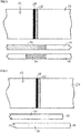
Figure 1 shows a cutaway view of an exemplary embodiment of the semiconductor device. -
Figures 2 ,3 ,4 ,5 and 6 show cutaway views of a part of exemplary embodiments of the semiconductor device. - In
figure 1 , a cutaway view of an exemplary embodiment of asemiconductor device 10 is shown. Thesemiconductor device 10 comprises a semiconductor body 11. The semiconductor body 11 comprises asubstrate 27. Thesubstrate 27 can, for example, comprise silicon. Furthermore, an electricallynon-conductive material 22 is arranged on thesubstrate 27 at a circuit side 24 of the semiconductor body 11. Within thenon-conductive material 22, other materials such as metals are arranged. Moreover, at the circuit side 24 of the semiconductor body 11 anintegrated circuit 18 is arranged. - An electrically conductive via 12 extends through the semiconductor body 11 and a part of the
non-conductive material 22. The via 12 has a main axis of extension which is perpendicular to the main plane of extension of thesubstrate 27. This means the main axis of extension of the via 12 is parallel to a vertical direction z which is perpendicular to the main plane of extension of thesubstrate 27. The via 12 has a lateral size which is given in a lateral direction x that is perpendicular to the vertical direction z. This means the lateral direction x is parallel to the main plane of extension of thesubstrate 27. The via 12 has atop side 13 which faces away from thenon-conductive material 22. Abottom side 14 of the via 12 is arranged at the side of the via 12 which faces away from thetop side 13 of the via 12. - The via 12 can be formed in the semiconductor body 11 by etching a
trench 20 in the semiconductor body 11 from acontact side 23 which faces away from thenon-conductive material 22. Thetrench 20 comprisesinner walls 21 which are coated with anisolation layer 26. Theisolation layer 26 is deposited at thetop side 13 of the via 12 such that also thesubstrate 27 is at least partially covered with theisolation layer 26. After the deposition of theisolation layer 26, theinner walls 21 of thetrench 20 are coated with an electricallyconductive contact material 28 which can be tungsten. After the deposition of thecontact material 28, apassivation layer 25 is deposited at theinner walls 21 of thetrench 20. Furthermore, a back contact 29 is deposited at thecontact side 23 of the semiconductor body 11 where the back contact 29 can be electrically contacted. The back contact 29 can comprise aluminum. Thecontact side 23 of the semiconductor body 11 is partially coated with anotherpassivation layer 25. - In this embodiment, the
trench 20 of the via 12 is not completely filled with theisolation layer 26, thepassivation layer 25 and thecontact material 28. This means the via 12 comprises an inner volume which is free of theisolation layer 26, thecontact material 28 and thepassivation layer 25. - At the
bottom side 14 of the via 12, an electrically conductive etch-stop layer 15 is arranged in a plane which is parallel to the lateral direction x. When thetrench 20 is etched in the semiconductor body 11, the material of the semiconductor body 11 and thenon-conductive material 22 is etched until the etch-stop layer 15. This means the etch-stop layer 15 acts as an etch stop for the etching of thetrench 20. - The etch-
stop layer 15 can be formed by aluminum or copper and the lateral extent in the lateral direction x of the etch-stop layer 15 amounts to 2.5 times the lateral extent of the via 12.Figure 1 is not drawn to scale. The etch-stop layer 15 is arranged symmetrically below the via 12 with respect to the vertical direction z. - Two electrically conductive contact layers 16 are arranged at the
bottom side 14 of the via 12 in a plane which is parallel to the lateral direction x and the etch-stop layer 15 is arranged between the via 12 and the contact layers 16 in vertical direction z. This means the twocontact layers 16 are arranged below the etch-stop layer 15 in vertical direction z and they are also symmetrically arranged with respect to the vertical direction z. The lateral extent in the lateral direction x of the contact layers 16 is smaller than the lateral extent of the via 12. The contact layers 16 can comprise copper and/or aluminum. - The
first contact layer 16 which is arranged between thesecond contact layer 16 and the etch-stop layer 15 is electrically connected with the etch-stop layer 15 by electricallyconductive connections 17 which extend in vertical direction z between the etch-stop layer 15 and thefirst contact layer 16. Thesecond contact layer 16 is electrically connected with thefirst contact layer 16 by theconnections 17 which extend in vertical direction z between the two contact layers 16. The etch-stop layer 15 is in mechanical and electrical contact with thecontact material 28 at thebottom side 14 of the via 12. The etch-stop layer 15, thecontact layer 16 and theconnections 17 are surrounded by thenon-conductive material 22. - If the
semiconductor device 10 is heated and cooled down again during processing, the metals of the etch-stop layer 15, thecontact layer 16 and thecontact material 28 of the via 12 show different thermal expansion than thenon-conductive material 22. Therefore, cracks can occur around the via 12. However, since the lateral extent in the lateral direction x of thecontact layer 16 is smaller than the lateral size of the via 12, the total area where a metal is in mechanical contact with thenon-conductive material 22 is decreased. If the lateral extent in the lateral direction x of thecontact layer 16 is below or above a critical size, no cracks are formed because of the difference in the coefficients of thermal expansion. Therefore, thesemiconductor device 10 can be operated more efficiently. - In the lateral direction x next to the
contact layer 16 and the etch-stop layer 15,several metal pads 31 can be arranged. In this case, themetal pads 31 are arranged in the same lateral planes as the etch-stop layer 15 and thecontact layer 16. Themetal pads 31 can comprise a metal as, for example, aluminum. Themetal pads 31 are electrically connected byconnections 17. It is possible that the contact layers 16 are electrically connected with one of themetal pads 31. It is possible that the contact layers 16 are electrically connected with themetal pads 31 in another plane through thesemiconductor device 10 which is not shown infigure 1 . Themetal pads 31 are electrically connected with an electrically conductivetop contact 32 of thesemiconductor device 10 and theintegrated circuit 18. Thetop contact 32 of thesemiconductor device 10 is arranged at atop contact side 33 of thesemiconductor device 10 which faces away from thecontact side 23 of the semiconductor body 11. Thetop contact 32 can have a thickness in vertical direction z that is larger than the thickness of the etch-stop layer 15 and of thecontact layer 16. - In
figure 2 , a schematic cutaway view of a part of an exemplary embodiment of thesemiconductor device 10 is shown. The via 12 is arranged within the semiconductor body 11 and theinner walls 21 of the via 12 are coated with anisolation layer 26 and thecontact material 28. The etch-stop layer 15 is arranged at thebottom side 14 of the via 12. Five contact layers 16 are also arranged at thebottom side 14 of the via 12. The lateral extent in the lateral direction x of the contact layers 16 amounts to at least 2.5 times the lateral extent of the via 12. Thecontact layer 16 which is the furthest away from the via 12 in vertical direction z is thicker in vertical direction z than the other contact layers 16. Moreover, thethicker contact layer 16 is structured with thenon-conductive material 22. It is structured in such a way that a grid structure of thethicker contact layer 16 is formed. Consequently, the probability of crack formation can be decreased since the total amount of metal is reduced. - In
figure 3 , a schematic cutaway view of a part of a further exemplary embodiment of thesemiconductor device 10 is shown. It is shown that the lateral extent in the lateral direction x of the etch-stop layer 15 amounts to at least 2.5 times the lateral extent of the via 12 in the lateral direction x. This means, the lateral extent of the etch-stop layer 15 can have any value which is larger than 2.5 times the lateral extent of the via 12 and which does not exceed the size of the semiconductor device. The region within the etch-stop layer 15 which is marked by dashed lines is anexclusion zone 34. This means, the lateral extent of the etch-stop layer 15 does not have any value which is within theexclusion zone 34. It is further shown that the lateral extent of thecontact layer 16 is smaller than the lateral extent of the via 12 or the lateral extent of thecontact layer 16 amounts to at least 2.5 times the lateral extent of the via 12. Anotherexclusion zone 34 arranged within thecontact layer 16 shows that the lateral extent of thecontact layer 16 does not have any value within theexclusion zone 34. - In
figure 4 , a schematic cutaway view of a part of a further exemplary embodiment of thesemiconductor device 10 is shown. The lateral extent of thecontact layer 16 in the lateral direction x is larger than the lateral extent of the etch-stop layer 15 in the lateral direction x. - In
figure 5 , a schematic cutaway view of a part of a further exemplary embodiment of thesemiconductor device 10 is shown. The lateral extent of the etch-stop layer 15 in the lateral direction x is larger than the lateral extent of thecontact layer 16 in the lateral direction x. - In
figure 6 , a schematic cutaway view of a part of a further exemplary embodiment of thesemiconductor device 10 is shown. Thesemiconductor device 10 comprises afurther contact layer 19. Thefurther contact layer 19 is arranged between the etch-stop layer 15 and thecontact layer 16 in vertical direction z. The lateral extent of thefurther contact layer 19 is smaller than the lateral extent of the via 12. Furthermore, the lateral extent of thefurther contact layer 19 can be smaller than the lateral extent of thecontact layer 16. Therefore, theexclusion zone 34 of thefurther contact layer 19 extends further in lateral direction x than theexclusion zone 34 of thecontact layer 16. -
- 10: semiconductor device
- 11: semiconductor body
- 12: via
- 13: top side
- 14: bottom side
- 15: etch-stop layer
- 16: contact layer
- 17: connection
- 18: integrated circuit
- 19: further contact layer
- 20: trench
- 21: inner wall
- 22: non-conductive material
- 23: contact side
- 24: circuit side
- 25: passivation layer
- 26: isolation layer
- 27: substrate
- 28: contact material
- 29: back contact
- 31: metal pad
- 32: top contact
- 33: top contact side
- 34: exclusion zone
- x: lateral direction
- z: vertical direction
Claims (12)
- Semiconductor device (10), comprising:- a semiconductor body (11),- an electrically conductive via (12) which extends through at least a part of the semiconductor body (11), and where the via (12) has a top side (13) and a bottom side (14) that faces away from the top side (13),- an electrically conductive etch-stop layer (15) arranged at the bottom side (14) of the via (12) in a plane which is parallel to a lateral direction (x), where the lateral direction (x) is perpendicular to a vertical direction (z) given by the main axis of extension of the via (12), and- at least one electrically conductive contact layer (16) at the bottom side (14) of the via (12) in a plane which is parallel to the lateral direction (x), wherein:- the etch-stop layer (16) is arranged between the electrically conductive via (12) and the contact layer (16) in the vertical direction (z),- the lateral extent in the lateral direction (x) of the etch-stop layer (15) amounts to at least 2.5 times the lateral extent of the via (12) in the lateral direction (x), and- the lateral extent of the contact layer (16) is smaller than the lateral extent of the via (12) or the lateral extent of the contact layer (16) amounts to at least 2.5 times the lateral extent of the via (12).
- Semiconductor device (10) according to claim 1, wherein the etch-stop layer (15) is arranged symmetrically with respect to the via (12).
- Semiconductor device (10) according to one of the preceding claims, wherein the contact layer (16) is arranged symmetrically with respect to the via (12).
- Semiconductor device (10) according to one of the preceding claims, wherein the lateral extent of the etch-stop layer (15) in the lateral direction (x) is larger than the lateral extent of the contact layer (16) in the lateral direction (x).
- Semiconductor device (10) according to one of the claims 1 to 3, wherein the lateral extent of the contact layer (16) in the lateral direction (x) is larger than the lateral extent of the etch-stop layer (15) in the lateral direction (x).
- Semiconductor device (10) according to one of the preceding claims, wherein at least one further contact layer (19) is arranged at the bottom side (14) of the via (12) in a plane which is parallel to the lateral direction (x).
- Semiconductor device (10) according to the preceding claim, wherein the lateral extent of the further contact layer (19) is smaller than the lateral extent of the via (12) or the lateral extent of the further contact layer (19) amounts to at least 2.5 times the lateral extent of the via (12) .
- Semiconductor device (10) according to one of the preceding claims, wherein the etch-stop layer (15) comprises copper and/or aluminum.
- Semiconductor device (10) according to one of the preceding claims, wherein the contact layer (16) comprises copper and/or aluminum.
- Semiconductor device (10) according to one of the preceding claims, wherein the etch-stop layer (15) and the contact layer (16) are electrically connected by at least one electrically conductive connection (17).
- Semiconductor device (10) according to one of the preceding claims, wherein at least one of the etch-stop layer (15) and the contact layer (16) is electrically connected with an integrated circuit (18) of the semiconductor device (10) .
- Semiconductor device (10) according to one of the preceding claims, wherein at least one of the at least one contact layer (16) is a structured layer which is structured with an electrically non-conductive material (22) in such a way that it is formed as a grid.
Priority Applications (5)
| Application Number | Priority Date | Filing Date | Title |
|---|---|---|---|
| EP18170639.1A EP3564994B1 (en) | 2018-05-03 | 2018-05-03 | Semiconductor device with through-substrate via |
| KR1020207031244A KR102456781B1 (en) | 2018-05-03 | 2019-03-20 | Semiconductor device with through-substrate vias |
| CN201980029058.XA CN112470269B (en) | 2018-05-03 | 2019-03-20 | Semiconductor device with through substrate via |
| US17/052,452 US11367672B2 (en) | 2018-05-03 | 2019-03-20 | Semiconductor device with through-substrate via |
| PCT/EP2019/056964 WO2019211041A1 (en) | 2018-05-03 | 2019-03-20 | Semiconductor device with through-substrate via |
Applications Claiming Priority (1)
| Application Number | Priority Date | Filing Date | Title |
|---|---|---|---|
| EP18170639.1A EP3564994B1 (en) | 2018-05-03 | 2018-05-03 | Semiconductor device with through-substrate via |
Publications (2)
| Publication Number | Publication Date |
|---|---|
| EP3564994A1 true EP3564994A1 (en) | 2019-11-06 |
| EP3564994B1 EP3564994B1 (en) | 2025-11-19 |
Family
ID=62116709
Family Applications (1)
| Application Number | Title | Priority Date | Filing Date |
|---|---|---|---|
| EP18170639.1A Active EP3564994B1 (en) | 2018-05-03 | 2018-05-03 | Semiconductor device with through-substrate via |
Country Status (5)
| Country | Link |
|---|---|
| US (1) | US11367672B2 (en) |
| EP (1) | EP3564994B1 (en) |
| KR (1) | KR102456781B1 (en) |
| CN (1) | CN112470269B (en) |
| WO (1) | WO2019211041A1 (en) |
Families Citing this family (1)
| Publication number | Priority date | Publication date | Assignee | Title |
|---|---|---|---|---|
| EP3564994B1 (en) * | 2018-05-03 | 2025-11-19 | ams AG | Semiconductor device with through-substrate via |
Citations (4)
| Publication number | Priority date | Publication date | Assignee | Title |
|---|---|---|---|---|
| US20140264881A1 (en) * | 2013-03-15 | 2014-09-18 | Analog Devices, Inc. | Methods and structures to facilitate through-silicon vias |
| US20150102497A1 (en) * | 2013-10-15 | 2015-04-16 | Jae-hwa Park | Integrated Circuit Devices Including a Through-Silicon Via Structure and Methods of Fabricating the Same |
| US20160351492A1 (en) * | 2015-05-29 | 2016-12-01 | Kabushiki Kaisha Toshiba | Semiconductor device and manufacturing method of semiconductor device |
| JP2017168732A (en) * | 2016-03-17 | 2017-09-21 | 株式会社デンソー | Semiconductor device |
Family Cites Families (10)
| Publication number | Priority date | Publication date | Assignee | Title |
|---|---|---|---|---|
| KR100335498B1 (en) * | 1999-12-22 | 2002-05-08 | 윤종용 | Fuse area structure in semiconductor device and forming method thereof |
| US7659595B2 (en) * | 2007-07-16 | 2010-02-09 | Taiwan Semiconductor Manufacturing Company, Ltd. | Embedded bonding pad for backside illuminated image sensor |
| US8368152B2 (en) * | 2011-04-18 | 2013-02-05 | Taiwan Semiconductor Manufacturing Company, Ltd. | MEMS device etch stop |
| JP5802515B2 (en) * | 2011-10-19 | 2015-10-28 | 株式会社東芝 | Semiconductor device and manufacturing method thereof |
| JP2013118264A (en) | 2011-12-02 | 2013-06-13 | Elpida Memory Inc | Semiconductor device and method of manufacturing the same |
| JP5922915B2 (en) * | 2011-12-02 | 2016-05-24 | ルネサスエレクトロニクス株式会社 | Semiconductor device and manufacturing method thereof |
| US9257392B2 (en) * | 2012-04-11 | 2016-02-09 | Mediatek Inc. | Semiconductor package with through silicon via interconnect |
| JP6489942B2 (en) * | 2015-05-29 | 2019-03-27 | 東芝メモリ株式会社 | Manufacturing method of semiconductor device |
| EP3364454B1 (en) * | 2017-02-15 | 2022-03-30 | ams AG | Semiconductor device |
| EP3564994B1 (en) * | 2018-05-03 | 2025-11-19 | ams AG | Semiconductor device with through-substrate via |
-
2018
- 2018-05-03 EP EP18170639.1A patent/EP3564994B1/en active Active
-
2019
- 2019-03-20 KR KR1020207031244A patent/KR102456781B1/en active Active
- 2019-03-20 WO PCT/EP2019/056964 patent/WO2019211041A1/en not_active Ceased
- 2019-03-20 CN CN201980029058.XA patent/CN112470269B/en active Active
- 2019-03-20 US US17/052,452 patent/US11367672B2/en active Active
Patent Citations (4)
| Publication number | Priority date | Publication date | Assignee | Title |
|---|---|---|---|---|
| US20140264881A1 (en) * | 2013-03-15 | 2014-09-18 | Analog Devices, Inc. | Methods and structures to facilitate through-silicon vias |
| US20150102497A1 (en) * | 2013-10-15 | 2015-04-16 | Jae-hwa Park | Integrated Circuit Devices Including a Through-Silicon Via Structure and Methods of Fabricating the Same |
| US20160351492A1 (en) * | 2015-05-29 | 2016-12-01 | Kabushiki Kaisha Toshiba | Semiconductor device and manufacturing method of semiconductor device |
| JP2017168732A (en) * | 2016-03-17 | 2017-09-21 | 株式会社デンソー | Semiconductor device |
Also Published As
| Publication number | Publication date |
|---|---|
| WO2019211041A1 (en) | 2019-11-07 |
| US20210175153A1 (en) | 2021-06-10 |
| EP3564994B1 (en) | 2025-11-19 |
| US11367672B2 (en) | 2022-06-21 |
| CN112470269B (en) | 2024-05-10 |
| CN112470269A (en) | 2021-03-09 |
| KR20200138791A (en) | 2020-12-10 |
| KR102456781B1 (en) | 2022-10-21 |
Similar Documents
| Publication | Publication Date | Title |
|---|---|---|
| US20240347511A1 (en) | Thermal pads between stacked semiconductor dies and associated systems and methods | |
| CN110875281B (en) | Wafer level system packaging method and packaging structure | |
| EP2106617B1 (en) | Trench isolation for reduced cross talk | |
| JP2008091852A (en) | Stacked package and manufacturing method thereof | |
| US11127656B2 (en) | Crack-resistant semiconductor devices | |
| US20120032339A1 (en) | Integrated circuit structure with through via for heat evacuating | |
| CN102790030B (en) | Semiconductor structure having offset passivation to reduce electromigration | |
| CN112670296B (en) | Three-dimensional memory structure and preparation method thereof | |
| US8643140B2 (en) | Suspended beam for use in MEMS device | |
| EP3564994B1 (en) | Semiconductor device with through-substrate via | |
| TWI793655B (en) | Conductive feature with non-uniform critical dimension and method of manufacturing the same | |
| US10340229B2 (en) | Semiconductor device with superior crack resistivity in the metallization system | |
| US11355386B2 (en) | Method for manufacturing a semiconductor device and semiconductor device | |
| KR20150097706A (en) | Surface modified TSV structure and methods thereof | |
| CN111868916A (en) | Integrated circuit (IC) device including a force mitigation system for reducing under-pad damage caused by wire bonding | |
| CN117727721A (en) | Wafer-based molded flip-chip routable IC packages | |
| CN112582364B (en) | Pad structure and forming method thereof, semiconductor device and forming method thereof | |
| TWI571964B (en) | Semiconductor structure and preparation method thereof | |
| US20250118692A1 (en) | Mitigating process problems in hybrid bonding of vertical die stacking | |
| KR20120022142A (en) | Semiconductor chip and method of fabricating the same | |
| KR20110065674A (en) | Manufacturing method of semiconductor device and semiconductor device using same |
Legal Events
| Date | Code | Title | Description |
|---|---|---|---|
| PUAI | Public reference made under article 153(3) epc to a published international application that has entered the european phase |
Free format text: ORIGINAL CODE: 0009012 |
|
| STAA | Information on the status of an ep patent application or granted ep patent |
Free format text: STATUS: THE APPLICATION HAS BEEN PUBLISHED |
|
| AK | Designated contracting states |
Kind code of ref document: A1 Designated state(s): AL AT BE BG CH CY CZ DE DK EE ES FI FR GB GR HR HU IE IS IT LI LT LU LV MC MK MT NL NO PL PT RO RS SE SI SK SM TR |
|
| AX | Request for extension of the european patent |
Extension state: BA ME |
|
| STAA | Information on the status of an ep patent application or granted ep patent |
Free format text: STATUS: REQUEST FOR EXAMINATION WAS MADE |
|
| 17P | Request for examination filed |
Effective date: 20200529 |
|
| RBV | Designated contracting states (corrected) |
Designated state(s): AL AT BE BG CH CY CZ DE DK EE ES FI FR GB GR HR HU IE IS IT LI LT LU LV MC MK MT NL NO PL PT RO RS SE SI SK SM TR |
|
| STAA | Information on the status of an ep patent application or granted ep patent |
Free format text: STATUS: EXAMINATION IS IN PROGRESS |
|
| 17Q | First examination report despatched |
Effective date: 20211103 |
|
| P01 | Opt-out of the competence of the unified patent court (upc) registered |
Effective date: 20230724 |
|
| GRAP | Despatch of communication of intention to grant a patent |
Free format text: ORIGINAL CODE: EPIDOSNIGR1 |
|
| STAA | Information on the status of an ep patent application or granted ep patent |
Free format text: STATUS: GRANT OF PATENT IS INTENDED |
|
| RIC1 | Information provided on ipc code assigned before grant |
Ipc: H01L 23/522 20060101ALI20250417BHEP Ipc: H01L 23/48 20060101AFI20250417BHEP |
|
| INTG | Intention to grant announced |
Effective date: 20250509 |
|
| RIN1 | Information on inventor provided before grant (corrected) |
Inventor name: SCHRANK, FRANZ Inventor name: COPPETA, RAFFAELE Inventor name: SINGULANI, ANDERSON Inventor name: PARTEDER, GEORG Inventor name: KRAFT, JOCHEN |
|
| GRAS | Grant fee paid |
Free format text: ORIGINAL CODE: EPIDOSNIGR3 |
|
| RIN1 | Information on inventor provided before grant (corrected) |
Inventor name: KRAFT, JOCHEN Inventor name: PARTEDER, GEORG Inventor name: SINGULANI, ANDERSON Inventor name: COPPETA, RAFFAELE Inventor name: SCHRANK, FRANZ |
|
| GRAA | (expected) grant |
Free format text: ORIGINAL CODE: 0009210 |
|
| STAA | Information on the status of an ep patent application or granted ep patent |
Free format text: STATUS: THE PATENT HAS BEEN GRANTED |
|
| AK | Designated contracting states |
Kind code of ref document: B1 Designated state(s): AL AT BE BG CH CY CZ DE DK EE ES FI FR GB GR HR HU IE IS IT LI LT LU LV MC MK MT NL NO PL PT RO RS SE SI SK SM TR |
|
| REG | Reference to a national code |
Ref country code: CH Ref legal event code: F10 Free format text: ST27 STATUS EVENT CODE: U-0-0-F10-F00 (AS PROVIDED BY THE NATIONAL OFFICE) Effective date: 20251119 Ref country code: GB Ref legal event code: FG4D |
|
| REG | Reference to a national code |
Ref country code: DE Ref legal event code: R079 Ref document number: 602018087239 Country of ref document: DE Free format text: PREVIOUS MAIN CLASS: H01L0023480000 Ipc: H10W0072000000 |
|
| REG | Reference to a national code |
Ref country code: DE Ref legal event code: R096 Ref document number: 602018087239 Country of ref document: DE |
|
| REG | Reference to a national code |
Ref country code: IE Ref legal event code: FG4D |
|
| REG | Reference to a national code |
Ref country code: NL Ref legal event code: MP Effective date: 20251119 |
|
| PG25 | Lapsed in a contracting state [announced via postgrant information from national office to epo] |
Ref country code: ES Free format text: LAPSE BECAUSE OF FAILURE TO SUBMIT A TRANSLATION OF THE DESCRIPTION OR TO PAY THE FEE WITHIN THE PRESCRIBED TIME-LIMIT Effective date: 20251119 |
|
| REG | Reference to a national code |
Ref country code: LT Ref legal event code: MG9D |
|
| PG25 | Lapsed in a contracting state [announced via postgrant information from national office to epo] |
Ref country code: NO Free format text: LAPSE BECAUSE OF FAILURE TO SUBMIT A TRANSLATION OF THE DESCRIPTION OR TO PAY THE FEE WITHIN THE PRESCRIBED TIME-LIMIT Effective date: 20260219 |
|
| PG25 | Lapsed in a contracting state [announced via postgrant information from national office to epo] |
Ref country code: AT Free format text: LAPSE BECAUSE OF FAILURE TO SUBMIT A TRANSLATION OF THE DESCRIPTION OR TO PAY THE FEE WITHIN THE PRESCRIBED TIME-LIMIT Effective date: 20251119 Ref country code: HR Free format text: LAPSE BECAUSE OF FAILURE TO SUBMIT A TRANSLATION OF THE DESCRIPTION OR TO PAY THE FEE WITHIN THE PRESCRIBED TIME-LIMIT Effective date: 20251119 Ref country code: FI Free format text: LAPSE BECAUSE OF FAILURE TO SUBMIT A TRANSLATION OF THE DESCRIPTION OR TO PAY THE FEE WITHIN THE PRESCRIBED TIME-LIMIT Effective date: 20251119 |
|
| REG | Reference to a national code |
Ref country code: AT Ref legal event code: MK05 Ref document number: 1859634 Country of ref document: AT Kind code of ref document: T Effective date: 20251119 |
|
| PG25 | Lapsed in a contracting state [announced via postgrant information from national office to epo] |
Ref country code: NL Free format text: LAPSE BECAUSE OF FAILURE TO SUBMIT A TRANSLATION OF THE DESCRIPTION OR TO PAY THE FEE WITHIN THE PRESCRIBED TIME-LIMIT Effective date: 20251119 |
|
| PG25 | Lapsed in a contracting state [announced via postgrant information from national office to epo] |
Ref country code: RS Free format text: LAPSE BECAUSE OF FAILURE TO SUBMIT A TRANSLATION OF THE DESCRIPTION OR TO PAY THE FEE WITHIN THE PRESCRIBED TIME-LIMIT Effective date: 20260219 |
|
| PG25 | Lapsed in a contracting state [announced via postgrant information from national office to epo] |
Ref country code: IS Free format text: LAPSE BECAUSE OF FAILURE TO SUBMIT A TRANSLATION OF THE DESCRIPTION OR TO PAY THE FEE WITHIN THE PRESCRIBED TIME-LIMIT Effective date: 20260319 |
|
| PG25 | Lapsed in a contracting state [announced via postgrant information from national office to epo] |
Ref country code: PT Free format text: LAPSE BECAUSE OF FAILURE TO SUBMIT A TRANSLATION OF THE DESCRIPTION OR TO PAY THE FEE WITHIN THE PRESCRIBED TIME-LIMIT Effective date: 20260319 |
|
| PG25 | Lapsed in a contracting state [announced via postgrant information from national office to epo] |
Ref country code: PL Free format text: LAPSE BECAUSE OF FAILURE TO SUBMIT A TRANSLATION OF THE DESCRIPTION OR TO PAY THE FEE WITHIN THE PRESCRIBED TIME-LIMIT Effective date: 20251119 |
|
| PG25 | Lapsed in a contracting state [announced via postgrant information from national office to epo] |
Ref country code: LV Free format text: LAPSE BECAUSE OF FAILURE TO SUBMIT A TRANSLATION OF THE DESCRIPTION OR TO PAY THE FEE WITHIN THE PRESCRIBED TIME-LIMIT Effective date: 20251119 |
|
| PG25 | Lapsed in a contracting state [announced via postgrant information from national office to epo] |
Ref country code: BG Free format text: LAPSE BECAUSE OF FAILURE TO SUBMIT A TRANSLATION OF THE DESCRIPTION OR TO PAY THE FEE WITHIN THE PRESCRIBED TIME-LIMIT Effective date: 20251119 |
|
| REG | Reference to a national code |
Ref country code: DE Ref legal event code: R081 Ref document number: 602018087239 Country of ref document: DE Owner name: AMS-OSRAM AG, AT Free format text: FORMER OWNER: AMS AG, PREMSTAETTEN, AT |
|
| PG25 | Lapsed in a contracting state [announced via postgrant information from national office to epo] |
Ref country code: LT Free format text: LAPSE BECAUSE OF FAILURE TO SUBMIT A TRANSLATION OF THE DESCRIPTION OR TO PAY THE FEE WITHIN THE PRESCRIBED TIME-LIMIT Effective date: 20251119 |
|
| PG25 | Lapsed in a contracting state [announced via postgrant information from national office to epo] |
Ref country code: SM Free format text: LAPSE BECAUSE OF FAILURE TO SUBMIT A TRANSLATION OF THE DESCRIPTION OR TO PAY THE FEE WITHIN THE PRESCRIBED TIME-LIMIT Effective date: 20251119 |
|
| PG25 | Lapsed in a contracting state [announced via postgrant information from national office to epo] |
Ref country code: DK Free format text: LAPSE BECAUSE OF FAILURE TO SUBMIT A TRANSLATION OF THE DESCRIPTION OR TO PAY THE FEE WITHIN THE PRESCRIBED TIME-LIMIT Effective date: 20251119 |
|
| PG25 | Lapsed in a contracting state [announced via postgrant information from national office to epo] |
Ref country code: IT Free format text: LAPSE BECAUSE OF FAILURE TO SUBMIT A TRANSLATION OF THE DESCRIPTION OR TO PAY THE FEE WITHIN THE PRESCRIBED TIME-LIMIT Effective date: 20251119 |
|
| PGFP | Annual fee paid to national office [announced via postgrant information from national office to epo] |
Ref country code: DE Payment date: 20260522 Year of fee payment: 9 |
|
| REG | Reference to a national code |
Ref country code: CH Ref legal event code: W10 Free format text: ST27 STATUS EVENT CODE: U-0-0-W10-W00 (AS PROVIDED BY THE NATIONAL OFFICE) Effective date: 20260715 |
|
| PG25 | Lapsed in a contracting state [announced via postgrant information from national office to epo] |
Ref country code: EE Free format text: LAPSE BECAUSE OF FAILURE TO SUBMIT A TRANSLATION OF THE DESCRIPTION OR TO PAY THE FEE WITHIN THE PRESCRIBED TIME-LIMIT Effective date: 20251119 |
|
| PG25 | Lapsed in a contracting state [announced via postgrant information from national office to epo] |
Ref country code: CZ Free format text: LAPSE BECAUSE OF FAILURE TO SUBMIT A TRANSLATION OF THE DESCRIPTION OR TO PAY THE FEE WITHIN THE PRESCRIBED TIME-LIMIT Effective date: 20251119 |
|
| PG25 | Lapsed in a contracting state [announced via postgrant information from national office to epo] |
Ref country code: SK Free format text: LAPSE BECAUSE OF FAILURE TO SUBMIT A TRANSLATION OF THE DESCRIPTION OR TO PAY THE FEE WITHIN THE PRESCRIBED TIME-LIMIT Effective date: 20251119 |
|
| PG25 | Lapsed in a contracting state [announced via postgrant information from national office to epo] |
Ref country code: SE Free format text: LAPSE BECAUSE OF FAILURE TO SUBMIT A TRANSLATION OF THE DESCRIPTION OR TO PAY THE FEE WITHIN THE PRESCRIBED TIME-LIMIT Effective date: 20251119 |
|
| RAP2 | Party data changed (patent owner data changed or rights of a patent transferred) |
Owner name: AMS-OSRAM AG |