EP3564974A1 - Flexible folding printed interconnect for reducing size of a surface mountable magnetic component for medical implantable devices - Google Patents
Flexible folding printed interconnect for reducing size of a surface mountable magnetic component for medical implantable devices Download PDFInfo
- Publication number
- EP3564974A1 EP3564974A1 EP19168478.6A EP19168478A EP3564974A1 EP 3564974 A1 EP3564974 A1 EP 3564974A1 EP 19168478 A EP19168478 A EP 19168478A EP 3564974 A1 EP3564974 A1 EP 3564974A1
- Authority
- EP
- European Patent Office
- Prior art keywords
- substrate
- transformer
- main part
- outer part
- wire
- Prior art date
- Legal status (The legal status is an assumption and is not a legal conclusion. Google has not performed a legal analysis and makes no representation as to the accuracy of the status listed.)
- Withdrawn
Links
Images


Classifications
-
- H—ELECTRICITY
- H01—ELECTRIC ELEMENTS
- H01F—MAGNETS; INDUCTANCES; TRANSFORMERS; SELECTION OF MATERIALS FOR THEIR MAGNETIC PROPERTIES
- H01F27/00—Details of transformers or inductances, in general
- H01F27/28—Coils; Windings; Conductive connections
- H01F27/2804—Printed windings
-
- H—ELECTRICITY
- H01—ELECTRIC ELEMENTS
- H01F—MAGNETS; INDUCTANCES; TRANSFORMERS; SELECTION OF MATERIALS FOR THEIR MAGNETIC PROPERTIES
- H01F27/00—Details of transformers or inductances, in general
- H01F27/06—Mounting, supporting, or suspending transformers, reactors, or choke coils not being of the signal type
-
- H—ELECTRICITY
- H01—ELECTRIC ELEMENTS
- H01F—MAGNETS; INDUCTANCES; TRANSFORMERS; SELECTION OF MATERIALS FOR THEIR MAGNETIC PROPERTIES
- H01F27/00—Details of transformers or inductances, in general
- H01F27/02—Casings
- H01F27/027—Casings specially adapted for combination of signal type inductors or transformers with electronic circuits, e.g. mounting on printed circuit boards
-
- H—ELECTRICITY
- H01—ELECTRIC ELEMENTS
- H01F—MAGNETS; INDUCTANCES; TRANSFORMERS; SELECTION OF MATERIALS FOR THEIR MAGNETIC PROPERTIES
- H01F27/00—Details of transformers or inductances, in general
- H01F27/06—Mounting, supporting, or suspending transformers, reactors, or choke coils not being of the signal type
- H01F27/065—Mounting on printed circuit boards
-
- H—ELECTRICITY
- H01—ELECTRIC ELEMENTS
- H01F—MAGNETS; INDUCTANCES; TRANSFORMERS; SELECTION OF MATERIALS FOR THEIR MAGNETIC PROPERTIES
- H01F27/00—Details of transformers or inductances, in general
- H01F27/24—Magnetic cores
-
- H—ELECTRICITY
- H01—ELECTRIC ELEMENTS
- H01F—MAGNETS; INDUCTANCES; TRANSFORMERS; SELECTION OF MATERIALS FOR THEIR MAGNETIC PROPERTIES
- H01F27/00—Details of transformers or inductances, in general
- H01F27/28—Coils; Windings; Conductive connections
- H01F27/2823—Wires
-
- H—ELECTRICITY
- H01—ELECTRIC ELEMENTS
- H01F—MAGNETS; INDUCTANCES; TRANSFORMERS; SELECTION OF MATERIALS FOR THEIR MAGNETIC PROPERTIES
- H01F41/00—Apparatus or processes specially adapted for manufacturing or assembling magnets, inductances or transformers; Apparatus or processes specially adapted for manufacturing materials characterised by their magnetic properties
- H01F41/02—Apparatus or processes specially adapted for manufacturing or assembling magnets, inductances or transformers; Apparatus or processes specially adapted for manufacturing materials characterised by their magnetic properties for manufacturing cores, coils, or magnets
- H01F41/04—Apparatus or processes specially adapted for manufacturing or assembling magnets, inductances or transformers; Apparatus or processes specially adapted for manufacturing materials characterised by their magnetic properties for manufacturing cores, coils, or magnets for manufacturing coils
- H01F41/041—Printed circuit coils
-
- H—ELECTRICITY
- H01—ELECTRIC ELEMENTS
- H01F—MAGNETS; INDUCTANCES; TRANSFORMERS; SELECTION OF MATERIALS FOR THEIR MAGNETIC PROPERTIES
- H01F41/00—Apparatus or processes specially adapted for manufacturing or assembling magnets, inductances or transformers; Apparatus or processes specially adapted for manufacturing materials characterised by their magnetic properties
- H01F41/02—Apparatus or processes specially adapted for manufacturing or assembling magnets, inductances or transformers; Apparatus or processes specially adapted for manufacturing materials characterised by their magnetic properties for manufacturing cores, coils, or magnets
- H01F41/04—Apparatus or processes specially adapted for manufacturing or assembling magnets, inductances or transformers; Apparatus or processes specially adapted for manufacturing materials characterised by their magnetic properties for manufacturing cores, coils, or magnets for manufacturing coils
- H01F41/06—Coil winding
-
- H—ELECTRICITY
- H05—ELECTRIC TECHNIQUES NOT OTHERWISE PROVIDED FOR
- H05K—PRINTED CIRCUITS; CASINGS OR CONSTRUCTIONAL DETAILS OF ELECTRIC APPARATUS; MANUFACTURE OF ASSEMBLAGES OF ELECTRICAL COMPONENTS
- H05K1/00—Printed circuits
- H05K1/02—Details
- H05K1/11—Printed elements for providing electric connections to or between printed circuits
- H05K1/115—Via connections; Lands around holes or via connections
Definitions
- the first and second contacts of the main part of the substrate are arranged on a bottom side of the main part, which bottom side faces away from the transformer.
- the assembly comprises at least one retention element for connecting the wound coil to the at least one outer part of the substrate so as to maintain the pivoted state of the at least one outer part.
- each end 101, 102 of the at least one primary wire 100 as well as each end 201, 202 of the at least one secondary wire 200 can be electrically connected with corresponding primary contacts 411, 412, and secondary contacts 421, 422 (cf. e.g. Figs. 2 , 4 and 5 ) of the first and second outer part 41, 42 of the substrate 4 without routing them longer distances, since the pivotable outer parts 41, 42 of the substrate directly face the transformer 2 and the wire ends 101, 102, 201, 202 protruding from the transformer 2.
- the transformer assembly 1' of this further embodiment may also comprise at least one retention element for securing the bobbin 3 to the outer part 41' of the substrate 4'
- at least one retention elements particularly serve for maintaining the pivoted state of the outer part 41.
Landscapes
- Engineering & Computer Science (AREA)
- Power Engineering (AREA)
- Manufacturing & Machinery (AREA)
- Microelectronics & Electronic Packaging (AREA)
- Coils Or Transformers For Communication (AREA)
Abstract
Description
- The invention relates to a transformer assembly and a method for producing such an assembly.
- Miniaturization of all components, including magnetics is required to remain competitive in the implantable medical device industry. Particularly, transformers are one of the largest components in implantable cardioverter-defibrillators (ICD) and are therefore important in any miniaturization effort. PCB-mounted transformers are typically large devices and one of the major reasons for this is that ends of the wires used in the windings are routed long distances to pins or other discrete connectors which also take up significant space. Particularly, wire wrapping around terminations and wire routing often requires valuable space in the X and Y directions. Further, when large terminations are present, it becomes difficult to automatically wind around the bobbin of the transformer.
- Thus, based on the above, the problem to be solved by the present invention is to provide a transformer assembly as well as a method for proving such an assembly that is improved regarding installation space.
- This problem is solved by a transformer assembly having the features of claim 1 as well as by a method having the features of claim 13. Embodiments of these aspects of the present invention are stated in the corresponding sub claims and are described below.
- According to claim 1, a transformer assembly is disclosed, comprising: an electrical transformer, the transformer comprising a wound coil, wherein the coil comprising at least one primary wire having two ends, and at least one secondary wire having two ends, the wires are wound around one single axis to form at least one primary winding (10) as well as at least one secondary winding of the transformer, a substrate for carrying the transformer, wherein the substrate comprises a main part as well as at least one outer part, wherein the main part carries the transformer and the at least one outer part of the substrate is hinged to the main part and is pivoted towards the transformer, and wherein each end of the at least one primary wire and each end of the at least one secondary wire is electrically connected to an assigned primary or secondary contact arranged on the at least one outer part.
- Thus, due to the invention, the wires do not need careful routing to the bottom of the bobbin for wire wrapping or connection or termination. Furthermore, particularly, the wires can be terminated immediately upon exiting the primary and secondary winding of the wound coil.
- Particularly, according to an embodiment of the transformer assembly according to the present invention, the at least one outer part of the substrate comprises a contact device like a slot, a hole or a contact pad assigned to each primary or secondary contact of the at least one outer part of the substrate for electrically contacting the respective end of the at least one primary wire and/or for electrically contacting the respective end of the at least one secondary wire.
- Further, according to an embodiment of the transformer assembly according to the present invention, the ends of the primary wire and/or the ends of the secondary wire are soldered or brazed or welded to the respective associated contact on the respective outer part of the substrate.
- Further, according to an embodiment of the transformer assembly according to the present invention, each of said parts of the substrate is formed as a printed circuit board, wherein the at least one outer part is hinged to the main part via a flexible member. Particularly, said flexible members can be flex cables or flex printed circuit boards that comprise sufficient flexibility so that they can be bent in order to pivot the outer parts of the substrate (e.g. PCB) towards the transformer.
- Particularly, according to an embodiment, the at least one outer parts of the substrate is pivoted towards the transformer such that they enclose an approximate right angle, preferably in the range of 80° to 100° with the main part of the substrate.
- Further, according to an embodiment of the transformer assembly according to the present invention, a conductor (e.g. conducting path, particularly PCB track) extends from each primary and secondary contact of the at least one outer part of the substrate to associated first and second contacts arranged on the main part of the substrate, particularly via said flexible member forming a hinge between the at least one outer part and the main part of the substrate, wherein the respective first contacts arranged on the main part of the substrate are configured for making electrical contact with the at least one primary wire and/or the respective second contacts arranged on the main part of the substrate are configured for making electrical contact with the at least one secondary wire.
- In an example, where the substrate has a main part and a first and a second outer part a conductor (e.g. conducting path, particularly PCB track) extends from each primary and secondary contact of the first outer part to an associated first contact arranged on the main part of the substrate, particularly via said flexible member forming a hinge between the first outer part and the main part of the substrate, wherein the respective first contact arranged on the main part of the substrate is configured for making electrical contact with the at least one primary wire, preferably with the ends of the at least one primary wire.
- Likewise, according to an embodiment of the transformer assembly according to the present invention, a conductor (e.g. conducting path, e.g. PCB track) extends from each primary and secondary contact of the second outer part to an associated second contact arranged on the main part of the substrate, particularly via said flexible member forming a hinge between the second outer part and the main part of the substrate, wherein the respective second contact arranged on the main part of the substrate is configured for making electrical contact with the at least one secondary wire, preferably with the ends of the at least one secondary wire.
- Further, according to an embodiment of the transformer assembly according to the present invention, the first and second contacts of the main part of the substrate are arranged on a bottom side of the main part, which bottom side faces away from the transformer.
- Particularly, the first and second contacts of the main part of the substrate are formed as Land Grid Array (LGA). Thus, the first and second contacts of the main part of the substrate preferably form a (e.g. standard) surface mount component configuration, such as LGA or pins. Other contact techniques may also be employed.
- Further, according to an embodiment of the transformer assembly according to the present invention, the assembly comprises at least one retention element for connecting the wound coil to the at least one outer part of the substrate so as to maintain the pivoted state of the at least one outer part.
- Further, according to an embodiment of the transformer assembly according to the present invention, the transformer assembly comprises an external clip member to maintain the pivoted state of the at least one outer part of the substrate. Said retention element(s) or said separate external clip thus help to maintain the overall shape, reduce the footprint further, and reduce tension on the wires.
- Further, according to an embodiment of the transformer assembly according to the present invention, the transformer comprises a core. Particularly, the core is a magnetic core and/or extends through a central opening wound coil.
- Yet another aspect of the present invention relates to a method for producing a transformer assembly according to the present invention, wherein the method comprises the steps of:
- providing an electrical transformer, the transformer comprising a wound coil, the wound coil is comprising at least a primary wire comprising two ends, and at least one secondary wire comprising two ends, which wires are wound to form at least one primary winding as well as at least one secondary winding of the transformer,
- providing a substrate for carrying the transformer, wherein the substrate comprises a main part as well as at least one outer part, whereby the at least one outer part is hinged to the main part of the substrate,
- arranging the transformer on the main part of the substrate,
- pivoting the at least one outer part of the substrate upwards and towards the transformer,
- electrically connecting each end of the at least one primary wire and each end of the at least one secondary wire to an associated contact arranged on the at least one outer part of the substrate.
- Further, according to an embodiment of the method according to the invention, the step of electrically contacting each end of the at least one primary wire to an associated primary contact arranged on one of the at least one outer part (first outer part) comprises arranging the respective end in, on or at an associated contact device like a slot, a hole or a contact pad assigned to the primary contact, which associated contact device is preferably formed in the first outer part of the substrate, particularly at an upper edge of the pivoted first part of the substrate.
- Further, in an embodiment, the step of electrically contacting each end of the at least one secondary wire to an associated secondary contact arranged on one of the at least one outer part (second outer part) comprises arranging the respective end in, on or at an associated contact device like a slot, a hole or a contact pad, which associated contact device is preferably formed in the second outer part of the substrate, particularly at an upper edge of the pivoted second part of the substrate.
- Further, in an embodiment, the step of electrically contacting each end of the at least one primary wire to its associated primary contact arranged on the first outer part comprises soldering the respective end to its associated contact device on the first outer part of the substrate.
- Further, according to an embodiment, the step of electrically contacting each end of the at least one secondary wire to its associated secondary contact arranged on the second outer part comprises soldering the respective end to its associated contact device on the second outer part of the substrate.
- Particularly, according to an embodiment, the step of providing an electrical transformer further comprises mounting the wound coil on a core, particularly such that the core extends through a central opening of the wound coil.
- Further, in an embodiment, after pivoting of the at least one outer parts of the substrate, the outer parts of the substrate are affixed and/or connected to the wound coil.
- In all embodiments, the wound coil can be a bobbin coil, which is known from the art.
- Due to the present invention, the overall size of the transformer assembly can be reduced. Further, the invention allows the use of standard terminations on the board (e.g. LGA or BGA).
- Furthermore, time and cost for making connections to the windings can be reduced and interconnect reliability is increased since wires no longer travel long distances. Furthermore, the labor processes required for winding and terminating can be designed and optimized for automation.
- This invention is also amenable to assembly of multiple transformers arrayed out on an easy to handle PCB with tie-ins to each transformer.
- Further features and embodiments of the present invention shall be described below with reference to the Figures, wherein
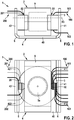
- Fig. 1
- shows a lateral view of a transformer assembly according to a first embodiment of the present invention;
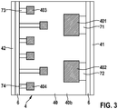
- Fig. 2
- shows a top view of the transformer assembly of
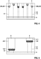
Fig. 1 ; - Fig. 3
- shows a plan view onto a bottom side of a main part of a substrate of the transformer assembly shown in
Figs. 1 and 2 ; - Fig. 4
- shows a lateral view of a pivotable second part of the substrate of the transformer assembly;
- Fig. 5
- shows a lateral view of a pivotable first part of the substrate of the transformer assembly; and
- Figs. 6 to 11
- show a process of producing the assembly shown in
Figs. 1 to 5 . - Fig. 12
- shows a lateral view of a transformer assembly according to a further embodiment of the present invention;
- Fig. 13
- shows a top view of the transformer assembly of
Fig. 12 ; - Fig. 14
- shows a plan view onto a bottom side of a main part of a substrate of the transformer assembly shown in
Figs. 12 and 13 ; -
Figure 1 shows in conjunction withFigs. 2 to 5 a transformer assembly 1 according to a first embodiment of the present invention. The assembly 1 comprises anelectrical transformer 2 which comprises abobbin 3 and particularly acore 9 that may be formed out of or comprises a material such as iron, ferrite, silicon steel or another suitable material. Thetransformer 2 further comprises at least oneprimary wire 100 comprising two ends 101, 102, and at least onesecondary wire 200 comprising two ends 201, 202. Particularly, thetransformer 2 may comprise any number and configuration of primary and secondary windings. In the following, for the sake of simplicity, only a primary and asecondary wire bobbin 3 to form a corresponding primary and secondary winding 10, 20. - Further, for carrying the
transformer 2, the assembly 1 comprises asubstrate 4, e.g. a printed circuit board (PCB), wherein thesubstrate 4 comprises amain part 40 which carries thetransformer 2 as well as a first and a secondouter part outer parts substrate 4 are hinged to themain part 40 and are pivoted towards thetransformer 2 as shown e.g. inFig. 1 , such that theouter parts substrate 4 enclose an angle in the range of e.g. 85° to 95° with themain part 40 of thesubstrate 4. Particularly, for allowing pivoting of theouter parts substrate 4 towards thetransformer 2, theouter parts main part 40 of thesubstrate 4 viaflexible members 6 serving as hinges, respectively. - Due to this pivoted arrangement of the
outer parts substrate 4, eachend primary wire 100 as well as eachend secondary wire 200 can be electrically connected with correspondingprimary contacts secondary contacts 421, 422 (cf. e.g.Figs. 2 ,4 and 5 ) of the first and secondouter part substrate 4 without routing them longer distances, since the pivotableouter parts transformer 2 and the wire ends 101, 102, 201, 202 protruding from thetransformer 2. - Particularly, as shown particularly in
Figs. 4 and 5 thefirst part 41 of thesubstrate 4 comprises contact devices in form of aslot 5 assigned to eachprimary contact first part 41 of thesubstrate 4 for receiving therespective end primary wire 100, while thesecond part 42 of thesubstrate 4 comprises contact devices in form of aslot 5 assigned to eachsecondary contact second part 42 of thesubstrate 4 for receiving therespective end secondary wire 200. - Particularly each of said
parts substrate 4 may be formed as a printed circuit board (PCB), wherein the firstouter part 41 is hinged to themain part 40 via a flexible member 6 (e.g. a flex PCB), and wherein the secondouter part 42 is hinged to themain part 40 via a flexible member 6 (e.g. a flex PCB). - Particularly, as further shown in
Fig. 3 ,4 and 5 , aconductor primary contact outer part 41 of thesubstrate 4 to an associated first contact arranged 401, 402 on themain part 40 of thesubstrate 4, wherein the respectivefirst contact main part 40 of thesubstrate 4 is configured for making electrical contact with the at least oneprimary wire 100. Likewise aconductor secondary contact outer part 42 of thesubstrate 4 to an associatedsecond contact main part 40 of thesubstrate 4, wherein the respectivesecond contact main part 40 of thesubstrate 4 is configured for making electrical contact with the at least onesecondary wire 200. - Particularly, as further indicated in
Fig. 3 , the set of contacts comprising first andsecond contacts main part 40 of thesubstrate 4 are arranged on abottom side 40b of themain part 40, whichbottom side 40b faces away from thetransformer 2. Particularly, the first andsecond contacts main part 40 of thesubstrate 4 are formed as LGA or BGA pads and are arranged insulated from thetransformer 2. - Optionally, as indicated in
Fig. 1 the transformer assembly 1 may comprise afirst retention element 81 for connecting thebobbin 3 to the firstouter part 41 of thesubstrate 4 as well as asecond retention element 82 for connecting thebobbin 3 to the secondouter part 42 of thesubstrate 4.Such retention elements outer part Fig. 1 ) may be used to maintain said pivoted state. - In addition to the
outer parts transformer 2 is at least laterally completely encased, preferred completely laterally and on top encased. - Furthermore,
Figs. 6 to 11 show an exemplary embodiment of the method according to the first embodiment of the present invention for producing/wiring a transformer assembly 1. - Here, as shown in
Fig. 6 , the transformer 2 (having e.g. abobbin 3, acore 9, and at least a primary and asecondary wire main part 40 of asubstrate 4 of the transformer assembly 1, wherein themain part 40 and the pivotable first and secondouter part substrate 4 are initially arranged in a flat configuration. - The wire ends 101, 102, 201, 202 are preferably arranged such that they extend upwards and do not interfere with the
outer parts Figs. 6 and7 ). - The
outer parts substrate 4 are then folded upwards and towards one another/towards thetransformer 2 as shown inFigs. 8 and 9 . Then, as shown inFigs. 10 and 11 the electrical connections between the first wire ends 101, 102 and the contact devices in form of aslot 5, assigned to theprimary contacts slot 5, assigned to thesecondary contacts respective contacts -
Figure 12 shows in conjunction withFigs. 13 and14 a transformer assembly 1' according to a further embodiment of the present invention. For all elements, which are identical and/or have the same function as the first embodiment, the references are used accordingly. These functions and elements have been already described and will not be addressed in detail in the description of this further embodiment. Like the first embodiment the assembly 1' comprises anelectrical transformer 2 which comprises abobbin 3 and particularly acore 9 that may be formed out of or comprises a material such as iron, ferrite, silicon steel or another suitable material. - The
transformer 2 in this further embodiment is carried by a substrate 4', e.g. a printed circuit board (PCB), wherein the substrate 4' comprises a main part 40' which carries thetransformer 2 as well as one outer part 41', which outer part 41' of the substrate 4' is hinged to the main part 40' and is pivoted towards thetransformer 2 as shown e.g. inFig. 12 , such that the outer part 41' of the substrate 4' enclose an angle in the range of e.g. 75° to 105° with the main part 40' of the substrate 4'. The outer part 41' is connected to the main part 40' of the substrate 4' viaflexible members 6 serving as hinges, respectively. - The
transformer 2 further comprises at least oneprimary wire 100 comprising two ends 101 and 102 (Fig. 13 ), and at least onesecondary wire 200 comprising two ends 201, 202. Because of this unilaterally arranged outer part 41' of the substrate 4', both the at least oneprimary wire 100 as well as the at least onesecondary wire 200 have to be fed out the transformer unilaterally, i.e. the side, where the outer part 41' of the substrate 4' is pivoted towards thetransformer 2. Eachend primary wire 100 as well as eachend secondary wire 200 can be electrically connected with corresponding primary contacts 411', 412', and secondary contacts 421', 422' (cf. e.g.Figs. 13 and14 ) of outer part 41', which is again possible, because the pivotable outer part 41' of the substrate 4' directly faces thetransformer 2 and the wire ends 101, 102, 201, 202 protruding from thetransformer 2. The primary contacts 411', 412' and secondary contacts 421', 422' are configured similarly than already described in respect toFigs. 4 and 5 of the first embodiment above. - Particularly each of said parts 40' and 41' of the substrate 4' may be formed as a printed circuit board (PCB), wherein the first outer part 41' is hinged to the main part 40' via a flexible member 6' (e.g. a flex PCB).
- Particularly, as further shown in
Fig. 14 , a conductor 71', 72' extends from each primary contact 411', 412' of the first outer part 41' of the substrate 4' to an associated first contact arranged 401', 402' on the main part 40' of the substrate 4', wherein the respective first contact 401', 402' arranged on the main part 40' of the substrate 4' is configured for making electrical contact with the at least oneprimary wire 100. Likewise a conductor 73', 74' extends from each secondary contact 421', 422' of the outer part 41' of the substrate 4' to an associated second contact 403', 404' arranged on the main part 40' of the substrate 4', wherein the respective second contact 403', 404' arranged on the main part 40' of the substrate 4' is configured for making electrical contact with the at least onesecondary wire 200. - Particularly, as further indicated in
Fig. 14 , the set of contacts comprising first and second contacts 401', 402', 403', 404' of the main part 40' of the substrate 4' are arranged on abottom side 40b' of the main part 40', whichbottom side 40b' faces away from thetransformer 2. Particularly, the first and second contacts 401', 402', 403', 404' of the main part 40' of the substrate 4' are formed as LGA or BGA pads and are arranged electrically insulated from thetransformer 2. - Optionally, as already indicated in
Fig. 1 , the transformer assembly 1' of this further embodiment may also comprise at least one retention element for securing thebobbin 3 to the outer part 41' of the substrate 4' Such at least one retention elements particularly serve for maintaining the pivoted state of theouter part 41. - All additional configurations of the first embodiments, which are not already mentioned relating to the further embodiment, may be combined in addition.
- Furthermore, the method for producing/wiring a transformer assembly 1 according to the first embodiment shown in
Figs. 6 to 11 applies to the further embodiment accordingly.
Claims (13)
- A transformer assembly (1, 1'), comprising:- an electrical transformer (2), the transformer (2) comprising a wound coil (3), wherein the coil comprising at least one primary wire (100) having two ends (101, 102), and at least one secondary wire (200) having two ends (201, 202), the wires (100, 200) are wound to form at least one primary winding (10) as well as at least one secondary winding (20) of the transformer (2),- a substrate (4, 4') for carrying the transformer (2), wherein the substrate (4, 4') comprises a main part (40, 40') as well as at least one outer part (41, 41', 42), wherein the main part (40, 40') carries the transformer (2) and the at least one outer part (41, 41', 42) of the substrate (4, 4') is hinged to the main part (40, 40') and is pivoted towards the transformer (2), wherein- each end (101, 102) of the at least one primary wire (100) and each end (201, 202) of the at least one secondary wire (200) is electrically connected to an assigned primary or secondary contact (411, 411', 412, 412', 421, 421', 422, 422') arranged on the at least one outer part (41, 41', 42).
- The transformer assembly according to claim 1, wherein the at least one outer part (41, 41', 42) of the substrate (4, 4') comprises a contact device (5) assigned to each primary or secondary contact (411, 411', 412, 412', 421, 421', 422, 422') of the at least one outer part (41, 41', 42) of the substrate (4, 4') for electrically contacting the respective end (101, 102) of the at least one primary wire (100) and/or for electrically contacting the respective end (201, 202) of the at least one secondary wire (200) .
- The transformer assembly according to claim 1 or 2, wherein each of said parts (40, 41, 41', 42) of the substrate (4, 4') is formed as a printed circuit board, wherein the at least one outer part (41, 41', 42) is hinged to the main part (40, 40') via a flexible member (6, 6').
- The transformer assembly according to one of the preceding claims, wherein the at least one outer part (41, 41', 42) of the substrate (4, 4') is pivoted towards the transformer (2) such that they enclose an angle in the range of 80° to 100° with the main part (40, 40') of the substrate (4, 4').
- The transformer assembly according to one of the preceding claims, wherein a conductor (71, 71', 72, 72', 73, 73', 74, 74') extends from each primary and secondary contact (411, 411', 412, 412', 421, 421', 422, 422') of the at least one outer part (41, 41', 42) of the substrate (4, 4') to associated first and second contacts (401, 401', 402, 402', 403, 403', 404, 404') arranged on the main part (40, 40') of the substrate (4, 4'), wherein the respective first contacts (401, 401', 402, 402') arranged on the main part (40, 40') of the substrate (4, 4') are configured for making electrical contact with the at least one primary wire (100) and/or the respective second contacts (403, 403', 404, 404') arranged on the main part (40, 40') of the substrate (4, 4') are configured for making electrical contact with the at least one secondary wire (200).
- The transformer assembly according to claim 5, wherein the first and second contacts (401, 401', 402, 402', 403, 403', 404, 404') of the main part (40, 40') of the substrate (4, 4') are arranged on a bottom side (40b, 40b') of the main part (40, 40'), which bottom side (40b, 40b') faces away from the transformer (2).
- The transformer assembly according to claim 5 or 6, wherein the first and second contacts (401, 401', 402, 402', 403, 403', 404, 404') of the main part (40, 40') of the substrate (4, 4') are formed as Land Grid Array or Ball Grid Array or pins.
- The transformer assembly according to one of the preceding claims, wherein the transformer assembly (1, 1') comprises at least one retention element (81, 82) for connecting the wound coil (3) to the at least one outer part (41, 41', 42) of the substrate (4) so as to maintain the pivoted state of the at least one outer part (41, 41', 42)
- The transformer assembly according to one of the preceding claims, wherein the transformer assembly (1, 1') comprises an external clip member (83) to maintain the pivoted state of the at least one outer part (41, 41', 42) of the substrate (4, 4').
- The transformer assembly according to one of the preceding claims, wherein the transformer (2) comprises a core (9).
- The transformer assembly according to claim 10, wherein the core (9) is a magnetic core.
- The transformer assembly according to claim 1, wherein the at least one primary wire (100) and the at least one secondary wire (200) are wound on a bobbin to form the at least one primary winding (10) as well as the at least one secondary winding (20) of the transformer (2) of the wound coil.
- Method for producing a transformer assembly (1, 1') according to one of the preceding claims, comprising the steps of:- providing an electrical transformer (2), the transformer (2) comprising a wound coil (3), the wound coil is comprising at least a primary wire (100) comprising two ends (101, 102), and at least one secondary wire (200) comprising two ends (201, 202), which wires (100, 200) are wound to form at least one primary winding (10) as well as at least one secondary winding (20) of the transformer (2),- providing a substrate (4, 4') for carrying the transformer (2), wherein the substrate (4, 4') comprises a main part (40, 40') as well as at least one outer part (41, 41', 42), whereby the at least one outer part (41, 41', 42) is hinged to the main part (40, 40') of the substrate (4, 4'),- arranging the transformer (2) on the main part (40, 40') of the substrate (4, 4'),- pivoting the at least one outer part (41, 41', 42) of the substrate (4, 4') upwards and towards the transformer (2),- electrically connecting each end (101, 102) of the at least one primary wire (100) and each end of the at least one secondary wire (200) to an associated contact (411, 411', 412, 412', 421, 421', 422, 422') arranged on the at least one outer part (41, 41', 42) of the substrate (4, 4').
Applications Claiming Priority (2)
| Application Number | Priority Date | Filing Date | Title |
|---|---|---|---|
| US201862663281P | 2018-04-27 | 2018-04-27 | |
| US201862672068P | 2018-05-16 | 2018-05-16 |
Publications (1)
| Publication Number | Publication Date |
|---|---|
| EP3564974A1 true EP3564974A1 (en) | 2019-11-06 |
Family
ID=66105090
Family Applications (1)
| Application Number | Title | Priority Date | Filing Date |
|---|---|---|---|
| EP19168478.6A Withdrawn EP3564974A1 (en) | 2018-04-27 | 2019-04-10 | Flexible folding printed interconnect for reducing size of a surface mountable magnetic component for medical implantable devices |
Country Status (2)
| Country | Link |
|---|---|
| US (1) | US20190333680A1 (en) |
| EP (1) | EP3564974A1 (en) |
Citations (4)
| Publication number | Priority date | Publication date | Assignee | Title |
|---|---|---|---|---|
| DE10124117A1 (en) * | 2001-05-17 | 2002-12-12 | Kathrein Werke Kg | Circuit board with contacted surface mount unit and associated surface mount units has SMD functional part that penetrates to below solder pad plane or lies beneath solder pad plane |
| US20100237972A1 (en) * | 2009-03-18 | 2010-09-23 | Chun-Ching Yen | Transformer structure |
| US20170164480A1 (en) * | 2015-12-08 | 2017-06-08 | Lite-On Electronics (Guangzhou) Limited | Transformer holder and electronic device using the same |
| WO2017141784A1 (en) * | 2016-02-18 | 2017-08-24 | 株式会社オートネットワーク技術研究所 | Circuit structure and electrical junction box |
-
2019
- 2019-04-10 EP EP19168478.6A patent/EP3564974A1/en not_active Withdrawn
- 2019-04-18 US US16/387,719 patent/US20190333680A1/en not_active Abandoned
Patent Citations (4)
| Publication number | Priority date | Publication date | Assignee | Title |
|---|---|---|---|---|
| DE10124117A1 (en) * | 2001-05-17 | 2002-12-12 | Kathrein Werke Kg | Circuit board with contacted surface mount unit and associated surface mount units has SMD functional part that penetrates to below solder pad plane or lies beneath solder pad plane |
| US20100237972A1 (en) * | 2009-03-18 | 2010-09-23 | Chun-Ching Yen | Transformer structure |
| US20170164480A1 (en) * | 2015-12-08 | 2017-06-08 | Lite-On Electronics (Guangzhou) Limited | Transformer holder and electronic device using the same |
| WO2017141784A1 (en) * | 2016-02-18 | 2017-08-24 | 株式会社オートネットワーク技術研究所 | Circuit structure and electrical junction box |
Also Published As
| Publication number | Publication date |
|---|---|
| US20190333680A1 (en) | 2019-10-31 |
Similar Documents
| Publication | Publication Date | Title |
|---|---|---|
| US4661792A (en) | Apparatus for mounting printed circuit boards | |
| US7874870B1 (en) | Coaxial cable connector with a connection terminal having a resilient tongue section | |
| US8758051B2 (en) | Connection structure and a connection method for connecting a differential signal transmission cable to a circuit board | |
| US8496499B2 (en) | Modular electronic header assembly and methods of manufacture | |
| JPH1126046A (en) | Clip for surface mount termination of coaxial cable | |
| US5309130A (en) | Self leaded surface mount coil lead form | |
| CN203706811U (en) | transformer assembly and power converter | |
| EP2717280A1 (en) | Transformer termination and interconnection assembly | |
| US3733574A (en) | Miniature tandem spring clips | |
| JP7490346B2 (en) | Coil device | |
| US20190333680A1 (en) | Flexible folding printed interconnect for reducing size of a surface mountable magnetic component for medical implantable devices | |
| US5262745A (en) | Surface mounted multi-section bobbin | |
| CN208128636U (en) | PCB and terminal | |
| US5203077A (en) | Method for mounting large discrete electronic components | |
| JPH026195B2 (en) | ||
| JPH118131A (en) | Transformer wiring structure | |
| US6565385B1 (en) | Reducing electromagnetic emissions from a connector coupled to a printed circuit board | |
| US8467194B2 (en) | AC adapter | |
| JP2002118019A (en) | Surface mount type winding parts | |
| US11315717B2 (en) | Inductive component | |
| JPH08162756A (en) | Device for connecting electronic module to mother board | |
| JP2020512702A (en) | Electric component, component device, and method of manufacturing component device | |
| JP2003031430A (en) | Small flyback transformer | |
| JPH062256Y2 (en) | Transformer parts | |
| JPH0629125A (en) | Electromagnetic device |
Legal Events
| Date | Code | Title | Description |
|---|---|---|---|
| PUAI | Public reference made under article 153(3) epc to a published international application that has entered the european phase |
Free format text: ORIGINAL CODE: 0009012 |
|
| STAA | Information on the status of an ep patent application or granted ep patent |
Free format text: STATUS: THE APPLICATION HAS BEEN PUBLISHED |
|
| AK | Designated contracting states |
Kind code of ref document: A1 Designated state(s): AL AT BE BG CH CY CZ DE DK EE ES FI FR GB GR HR HU IE IS IT LI LT LU LV MC MK MT NL NO PL PT RO RS SE SI SK SM TR |
|
| AX | Request for extension of the european patent |
Extension state: BA ME |
|
| STAA | Information on the status of an ep patent application or granted ep patent |
Free format text: STATUS: REQUEST FOR EXAMINATION WAS MADE |
|
| 17P | Request for examination filed |
Effective date: 20200427 |
|
| RBV | Designated contracting states (corrected) |
Designated state(s): AL AT BE BG CH CY CZ DE DK EE ES FI FR GB GR HR HU IE IS IT LI LT LU LV MC MK MT NL NO PL PT RO RS SE SI SK SM TR |
|
| STAA | Information on the status of an ep patent application or granted ep patent |
Free format text: STATUS: EXAMINATION IS IN PROGRESS |
|
| 17Q | First examination report despatched |
Effective date: 20201123 |
|
| GRAP | Despatch of communication of intention to grant a patent |
Free format text: ORIGINAL CODE: EPIDOSNIGR1 |
|
| STAA | Information on the status of an ep patent application or granted ep patent |
Free format text: STATUS: GRANT OF PATENT IS INTENDED |
|
| INTG | Intention to grant announced |
Effective date: 20230307 |
|
| STAA | Information on the status of an ep patent application or granted ep patent |
Free format text: STATUS: THE APPLICATION IS DEEMED TO BE WITHDRAWN |
|
| 18D | Application deemed to be withdrawn |
Effective date: 20230718 |