EP3564579A1 - Light distribution element, light source module and lighting device - Google Patents
Light distribution element, light source module and lighting device Download PDFInfo
- Publication number
- EP3564579A1 EP3564579A1 EP18808896.7A EP18808896A EP3564579A1 EP 3564579 A1 EP3564579 A1 EP 3564579A1 EP 18808896 A EP18808896 A EP 18808896A EP 3564579 A1 EP3564579 A1 EP 3564579A1
- Authority
- EP
- European Patent Office
- Prior art keywords
- light
- light emitting
- distribution element
- incident surface
- emitting surface
- Prior art date
- Legal status (The legal status is an assumption and is not a legal conclusion. Google has not performed a legal analysis and makes no representation as to the accuracy of the status listed.)
- Granted
Links
Images



Classifications
-
- F—MECHANICAL ENGINEERING; LIGHTING; HEATING; WEAPONS; BLASTING
- F21—LIGHTING
- F21V—FUNCTIONAL FEATURES OR DETAILS OF LIGHTING DEVICES OR SYSTEMS THEREOF; STRUCTURAL COMBINATIONS OF LIGHTING DEVICES WITH OTHER ARTICLES, NOT OTHERWISE PROVIDED FOR
- F21V5/00—Refractors for light sources
- F21V5/04—Refractors for light sources of lens shape
- F21V5/048—Refractors for light sources of lens shape the lens being a simple lens adapted to cooperate with a point-like source for emitting mainly in one direction and having an axis coincident with the main light transmission direction, e.g. convergent or divergent lenses, plano-concave or plano-convex lenses
-
- F—MECHANICAL ENGINEERING; LIGHTING; HEATING; WEAPONS; BLASTING
- F21—LIGHTING
- F21V—FUNCTIONAL FEATURES OR DETAILS OF LIGHTING DEVICES OR SYSTEMS THEREOF; STRUCTURAL COMBINATIONS OF LIGHTING DEVICES WITH OTHER ARTICLES, NOT OTHERWISE PROVIDED FOR
- F21V5/00—Refractors for light sources
- F21V5/007—Array of lenses or refractors for a cluster of light sources, e.g. for arrangement of multiple light sources in one plane
-
- F—MECHANICAL ENGINEERING; LIGHTING; HEATING; WEAPONS; BLASTING
- F21—LIGHTING
- F21S—NON-PORTABLE LIGHTING DEVICES; SYSTEMS THEREOF; VEHICLE LIGHTING DEVICES SPECIALLY ADAPTED FOR VEHICLE EXTERIORS
- F21S8/00—Lighting devices intended for fixed installation
- F21S8/08—Lighting devices intended for fixed installation with a standard
- F21S8/085—Lighting devices intended for fixed installation with a standard of high-built type, e.g. street light
- F21S8/086—Lighting devices intended for fixed installation with a standard of high-built type, e.g. street light with lighting device attached sideways of the standard, e.g. for roads and highways
-
- F—MECHANICAL ENGINEERING; LIGHTING; HEATING; WEAPONS; BLASTING
- F21—LIGHTING
- F21V—FUNCTIONAL FEATURES OR DETAILS OF LIGHTING DEVICES OR SYSTEMS THEREOF; STRUCTURAL COMBINATIONS OF LIGHTING DEVICES WITH OTHER ARTICLES, NOT OTHERWISE PROVIDED FOR
- F21V5/00—Refractors for light sources
- F21V5/04—Refractors for light sources of lens shape
-
- F—MECHANICAL ENGINEERING; LIGHTING; HEATING; WEAPONS; BLASTING
- F21—LIGHTING
- F21W—INDEXING SCHEME ASSOCIATED WITH SUBCLASSES F21K, F21L, F21S and F21V, RELATING TO USES OR APPLICATIONS OF LIGHTING DEVICES OR SYSTEMS
- F21W2131/00—Use or application of lighting devices or systems not provided for in codes F21W2102/00-F21W2121/00
- F21W2131/10—Outdoor lighting
- F21W2131/103—Outdoor lighting of streets or roads
-
- F—MECHANICAL ENGINEERING; LIGHTING; HEATING; WEAPONS; BLASTING
- F21—LIGHTING
- F21Y—INDEXING SCHEME ASSOCIATED WITH SUBCLASSES F21K, F21L, F21S and F21V, RELATING TO THE FORM OR THE KIND OF THE LIGHT SOURCES OR OF THE COLOUR OF THE LIGHT EMITTED
- F21Y2105/00—Planar light sources
- F21Y2105/10—Planar light sources comprising a two-dimensional [2D] array of point-like light-generating elements
- F21Y2105/14—Planar light sources comprising a two-dimensional [2D] array of point-like light-generating elements characterised by the overall shape of the two-dimensional [2D] array
- F21Y2105/16—Planar light sources comprising a two-dimensional [2D] array of point-like light-generating elements characterised by the overall shape of the two-dimensional [2D] array square or rectangular, e.g. for light panels
-
- F—MECHANICAL ENGINEERING; LIGHTING; HEATING; WEAPONS; BLASTING
- F21—LIGHTING
- F21Y—INDEXING SCHEME ASSOCIATED WITH SUBCLASSES F21K, F21L, F21S and F21V, RELATING TO THE FORM OR THE KIND OF THE LIGHT SOURCES OR OF THE COLOUR OF THE LIGHT EMITTED
- F21Y2115/00—Light-generating elements of semiconductor light sources
- F21Y2115/10—Light-emitting diodes [LED]
Definitions
- the present invention relates to a field of lighting technology, especially to a light distribution element, a light source module and a lighting device.
- a light device generally comprises a light source module, a power source module for providing power for the light source module, and a substrate for supporting the light source module and the power source module.
- the light source module generally comprises a light emitting unit and a light distribution element covering in a light emitting direction of the light emitting unit, and the light distribution element can adjust a direction of light emitted by the light emitting unit to realize illumination on a target area.
- Embodiments of the present invention aim to provide a light distribution element, a light source module and a lighting device, to solve the above problems.
- the embodiments of the present invention provide a light distribution element, comprising: a light incident surface, which is in a shape of a smooth inward concave curved surface and forms an accommodation cavity for accommodating a light emitting unit; and a light emitting surface, which is in a shape of a smooth outward convex curved surface and is opposite to the light incident surface.
- a thickness difference is between the light incident surface and the light emitting surface, and in a light spot formed by light emitted from the light emitting surface located on a portion with a larger thickness, a color tolerance between a yellow spot and white light is less than a preset color difference.
- the preset color difference is 4.
- an offset distance between a center of the light emitting unit and a center point of the light emitting surface is 20% of a width of the light emitting unit.
- an offset distance between a center of the light emitting unit and a center point of the light emitting surface is within a range of 0.55 mm.
- the light emitting surface comprises a center point, the center point of the light emitting surface is staggered with a center point of the light incident surface in a vertical direction.
- the embodiments of the present invention provide a light distribution element, comprising: a light incident surface, which is in a shape of a smooth inward concave curved surface and forms an accommodation cavity for accommodating a light emitting unit, and comprises a center point; and a light emitting surface, which is in a shape of a smooth outward convex curved surface and is opposite to the light incident surface, and comprises a center point.
- the center point of the light emitting surface is staggered with the center point of the light incident surface in a vertical direction, and the center point of the light emitting surface is aligned with the light emitting unit located in the accommodation cavity in the vertical direction.
- the center point of the light incident surface is a highest point of the light incident surface
- the center point of the light emitting surface is a highest point of the light emitting surface
- each of the light incident surface and the light emitting surface has a cross cutting line and a rip cutting line for dividing into four quadrants, and both the light incident surface and the light emitting surface are symmetric in the four quadrants.
- a thickness between the light incident surface and the light emitting surface is characterized in that the thickness is minimum between the center point of the light emitting surface and the light incident surface, and from the center point to two sides of the light emitting surface, the thickness between the light emitting surface and the light incident surface increases symmetrically.
- a thickness between the light incident surface and the light emitting surface is in an increasing tendency.
- a projection of the cross cutting line of the light incident surface on a horizontal plane is shorter than a projection of the rip cutting line of the light incident surface on the horizontal plane.
- a projection of the cross cutting line of the light emitting surface on a horizontal plane is longer than a projection of the rip cutting line of the light emitting surface on the horizontal plane.
- a projection of the cross cutting line of the light incident surface on a horizontal plane is parallel to a projection of the cross cutting line of the light emitting surface on the horizontal plane.
- a distance between a projection of the rip cutting line of the light incident surface on a horizontal plane and a projection of the rip cutting line of the light emitting surface on the horizontal plane is less than a preset line distance threshold value.
- the projection of the rip cutting line of the light incident surface on the horizontal plane coincides with the projection of the rip cutting line of the light emitting surface on the horizontal plane.
- a ratio between a projection of the cross cutting line and a projection of the rip cutting line on a horizontal plane in the light incident surface is greater than a ratio between a projection of the cross cutting line and a projection of the rip cutting line on the horizontal plane of the light emitting surface.
- a point distance between a portion of an edge of the light incident surface and a portion of an edge of the light emitting surface is less than a preset point distance threshold value.
- At least a part of the edge of the light incident surface coincides with a part of the edge of the light emitting surface.
- the light distribution element comprises a bottom surface surrounding a peripheral side of the light incident surface and the bottom surface is flat.
- the light distribution element comprises a top surface surrounding a peripheral side of the light emitting surface, and the bottom surface and the top surface are disposed in parallel and are connected with each other by a side surface to form a mounting part.
- the embodiments of the present invention provide a light source module, comprising: a substrate, a light emitting unit, provided on the substrate, and the above-mentioned light distribution element.
- the light distribution element is mounted to the substrate and covered on the light emitting unit, and the light emitting unit is located in the accommodation cavity of the light distribution element and is aligned with a center point of the light emitting surface in a vertical direction.
- the light source module comprises a plurality of light distribution elements and a plurality of light emitting units, the plurality of light emitting units are arranged on the substrate in an array, and at least one light emitting unit is provide within each of the plurality of light distribution elements.
- an offset direction of a center point of the light incident surface is identical to an offset direction of the center point of the light emitting surface in each light distribution element.
- a distance between the light distribution elements in a same row or a same column is same.
- the substrate comprises a lengthwise direction
- the substrate comprises a light source accommodation region and a mounting region which are sequentially arranged along the lengthwise direction
- the light emitting unit is in the light source accommodation region.
- the embodiments of the present invention provide a lighting device, comprising: a power source module, and at least one of the above mentioned light source modules.
- the light source module is electrically connected with the power source module.
- the lighting device is a street lamp.
- the lighting device further comprises a housing, and the power source module and the light source module are mounted to the housing; the lighting device further comprises a vertical supporting arm connected with the housing.
- the light incident surface and the light emitting surface of the light distribution element are both smooth curved surfaces and a thickness difference is between the light incident surface and the light emitting surface; in a light spot formed by light emitted from the light emitting surface located on a portion with a larger thickness, an area of a yellow spot is larger than a preset area.
- the concentration of the yellow light is decreased by presetting the size of the preset area, thereby weakening the yellow spot and ensuring the illumination effect of the lighting device.
- the lighting device 1000 includes a light source module 100 and a power source module 200 (referring to FIG. 3 ) which are electrically connected with each other.
- the power source module 200 may obtain power from commercial power or an external battery, and then transport the power to the light source module 100; the light source module 100 emits light rays after obtaining the power to illuminate a preset area.
- both the light source module 100 and the power source module 200 may be located on a housing 300
- the lighting device 1000 may be a street lamp or another type of a residential or outdoor lamp
- the shape and material of the housing 300 may be determined based on the type and application environment of the lighting device 1000.
- the housing 300 may also be set according to the conventional shape of the street lamp.
- the lighting device further includes a vertical supporting arm (not shown), mounted to a base board, a road surface, or the like.
- this vertical supporting arm is a lamp post.
- the housing 300 includes a mounting tail end 310 for connecting the vertical supporting arm (not shown).
- the mounting tail end 310 may be in a shape of hollow tube, and commercial cables may be electrically connected with the light source module 100 and the power source module 200 through the vertical supporting arm and an interior of the mounting tail end 310. In practical use, the mounting tail end 310 may be connected with the vertical supporting arm using screws or the like.
- a number of the light source module 100 may be at least one; the power source module 200 may include a current regulation unit, an overcurrent protection unit, or the like, and the power source module 200 may be in patch or plug-in type, which is not repeated herein.
- the light source module 100 includes light distribution elements 10, light emitting units 20 and a substrate 30.
- the substrate 30 is mounted into the housing 300, a plurality of light emitting units 20 are arranged on the substrate 30 in an array, a plurality of light distribution elements 10 are also arranged on the substrate 30 in an array, and each of the light distribution elements 10 is covered on at least one light emitting unit 20.
- the light distribution elements 10 are connected with one another by means of light transmitting materials. In practical applications, the satisfactory number of light distribution elements 10 with desired layouts may be formed in one piece by injection moulding.
- the power source module 200 is also located on the substrate 30 and is electrically connected with the light emitting unit 20 through an electrical element in the substrate 30.
- the substrate 30 includes a lengthwise direction, and a light source accommodation region 31 and a mounting region 32 which are sequentially arranged along the lengthwise direction, and the light emitting units 20 and the light distribution elements 10 are all located in the light source accommodation region 31, and the power supply module 200 is located in the mounting region 32.
- the light distribution element 10 is mainly configured for regulating angle and direction of the light ray emitted from the light emitting unit 20.
- the light distribution element 10 may be made of a transparent material, such as polycarbonate PC, polymethyl methacrylate PMMA, or the like, and the size of the light distribution element 10 may also be adjusted adaptively according to an application scenario of the light source module 100 and lighting demands, which are not repeated herein.
- the light distribution element 10 includes a light incident surface 11 and a light emitting surface 12 which are arranged opposite to each other. Both the light incident surface 11 and the light emitting surface 12 are in a shape of a smooth curved surface. That is, no obvious deformation occurs on the light incident surface 11 and the light emitting surface 12, and the deformation herein may refer to a protrusion, a depression, or their combination.
- the "obvious deformation” herein may refer to the deformation which may be recognized by human eyes or touched and perceived by fingers, or the limited lighting effect caused by the great influence of the deformation on the light ray adjustment of the light distribution element 10, without generally referring to all types of deformations.
- the light incident surface 11 or the light emitting surface 12 may be considered as smooth; in a case where the deformation on the light incident surface 11 or the light emitting surface 12 cannot be recognized by human eyes or touched and perceived by fingers, the light incident surface 11 or the light emitting surface 12 may also be considered as smooth.
- whether the above-mentioned deformation affects the light distribution of the light distribution element 10 may be judged by physically or artificially comparing the light distribution element with such a deformation, with the light distribution element without such a deformation (an optimal light distribution element provided by the inventor), so as to determine whether a difference in light distribution effect therebetween is within an acceptable range.
- the "acceptable range” herein may be set by inventors based on the lighting scenario or user demands, without generally referring to a general standard suitable for any user or scenario. Certainly, in the case of the deformation which may be touched and perceived by fingers of a related testing personnel or seen by human eyes, this light incident surface 11 or the light emitting surface 12 is considered as not smooth.
- the light incident surface 11 is in a shape of an inward concave curved surface and forms an accommodation cavity 13 for accommodating the light emitting unit 20, the light ray emitted from the light emitting unit 20 arrives at the light incident surface 11, and then is emitted out through the light emitting surface 12.
- the light emitting surface 12 is in a shape of an outward convex curved surface and protrudes in a direction the same as the direction in which the light incident surface 11 is concaved.
- the light incident surface 11 and the light emitting surface 12 are both in a shape of a partial spherical surface substantially.
- the "shape of partial spherical surface” herein may be obtained by cutting a whole spherical surface, or may be formed by splicing several partial spherical surfaces, so long as the light incident surface 11 and the light emitting surface 12 are guaranteed to be smooth.
- the light distribution element 10 may further include a bottom surface 14 located at a peripheral side of the light incident surface 11.
- the bottom surface 14 is flat and is configured for being directed attached to the substrate 30, so as to cover the light distribution element 10 on the light emitting unit 20. Even if an overlarge distance exists between the light distribution element 10 and the substrate 30 due to an assembly problem, the light rays can be only emitted from the light distribution element 10, which avoids negative optical effects, such as crescent bright spots.
- the light distribution element 10 further includes a top surface 15 located at a peripheral side of the light emitting surface 12, the top surface 15 is arranged parallel with the bottom surface 14, and is connected with the bottom surface 14 by means of a side surface 16 to form a square mounting portion.
- the light source module 100 includes a plurality of light distribution elements 10
- these light distribution elements may be connected with the substrate 30 using screws or in a snap-joint manner, or with the housing 300, which is well-known by persons skilled in the art, and is not repeated herein.
- FIG. 6 is a sectional view of a part of the light source module shown in FIG. 4 in A-A direction.
- the plane where the A-A direction is located may be understood as a horizontal plane, and in this situation, the light source module 100 is also arranged on the horizontal plane.
- the shapes of the light incident surface 11 and the light emitting surface 12 on the horizontal plane will be described in detail below with reference to the sectional view of FIG. 6 .
- the light incident surface 11 has a light incident edge 111
- the light emitting surface 12 has a light emitting edge 121
- the light incident edge 111 and the light emitting edge 121 indicate the substantial shapes of the light incident surface 11 and the light emitting surface 12 respectively.
- a profile of the light incident edge 111 reflects a projection of the light incident surface 11 on the horizontal plane.
- the light incident edge 111 is circular
- the light incident surface 11 is a partial spherical surface
- the light incident surface 11 is a partial ellipsoidal surface.
- a point distance between a portion of the light incident edge 111 and a portion of the light emitting edge 121 is less than a preset point distance threshold value which may be set in advance, for example, as 1 millimeter or other values.
- the preset point distance threshold value may be set very small, such that the light incident edge 111 and the light emitting edge 121 are overlapped basically or exactly at some points.
- the light incident surface 11 and the light emitting surface 12 both include a cross cutting line and a rip cutting line for dividing into four quadrants, wherein the cross cutting line is a cutting line in the middle along a crosswise direction of the light incident surface 11 or the light emitting surface 12, and the rip cutting line is a cutting line in the middle along a lengthwise direction of the light incident surface 11 or the light emitting surface 12.
- the cross and rip cutting lines are virtual lines for the subsequent detailed description about the technical solutions, without limiting the shapes of the light incident surface 11 and the light emitting surface 12.
- the cut light incident surface 11 and the light emitting surface 12 are symmetric in the four quadrants.
- the light incident surface 11 which is symmetric in the four quadrants as an example, it is indicated that the light incident surface 11 is divided into four parts after cut in crosswise and lengthwise directions, and any two of the four parts are symmetric axially or centrally.
- the parts located in the first and second quadrants are symmetric axially, and the parts located in the first and third quadrants are symmetric centrally.
- the "symmetric in the four quadrants" herein does not refer in particular to the absolute symmetry mathematically, but may include approximate symmetry. Still taking the light incident surface 11 as an example, at least two of the four parts are symmetric approximately, for example, the parts in the first and second quadrants are symmetric axially approximately, or the parts in the first and third quadrants are symmetric centrally approximately, and even the parts in the first and second quadrants are symmetric axially approximately, and the parts in the first and third quadrants are symmetric centrally approximately.
- the projections of the cross and rip cutting lines, for dividing the light incident surface 11 into four quadrants, on the horizontal plane are set to be the light incident cross cutting line 112 and the light incident rip cutting line 113
- the projections of the cross and rip cutting lines, for dividing the light emitting surface 12 into four quadrants, on the horizontal plane are set to be the light emitting cross cutting line 122 and the light emitting rip cutting line 123.
- a length of the light incident cross cutting line 112 is less than that of the light incident rip cutting line 13, i.e., the projection of the light incident surface 11 on the horizontal plane is preferably in a shape of oval or an approximate oval.
- a length of the light emitting cross cutting line 122 is greater than that of the light emitting rip cutting line 123, i.e., the projection of the light emitting surface 12 on the horizontal plane is preferably in a shape of oval or an approximate oval.
- a ratio between the light incident rip cutting line 113 and the light incident cross cutting line 112 is greater than a ratio between the light emitting rip cutting line 123 and the light emitting cross cutting line 122, such that the light incident surface 11 is longer and narrower than the light emitting surface 12.
- the light incident cross cutting line 112 is parallel with the light emitting cross cutting line 122. It should be noted that the parallelism herein does not refer to the absolute parallelism in the sense of data, and may also include approximate parallelism, which is not repeated herein. Moreover, the distance between the light incident rip cutting line 113 and the light emitting rip cutting line 123 is less than a preset line distance threshold value which may be set in advance, for example, as 1 millimeter or other values. In practical use, the preset point distance threshold value may be set to be very small, such that the light incident rip cutting line 113 and the light emitting rip cutting line 123 are overlapped basically or exactly.
- the light incident surface 11 and the light emitting surface 12 both have center points.
- the center point is a middle point or a highest point of the surface.
- the projection of the center point of the light incident surface 11 on the horizontal plane is an intersection point between the light incident rip cutting line 113 and the light incident cross cutting line 112
- the projection of the center point of the light emitting surface 12 on the horizontal plane is an intersection point between the light emitting rip cutting line 123 and the light emitting cross cutting line 122.
- the center point of the light incident surface 11 and the center point of the light emitting surface 12 are staggered with each other in a vertical direction; that is, a connection line therebetween is not along the vertical direction.
- a thickness between the light incident surface 11 and the light emitting surface 12 is characterized in that the thickness is minimum between the center point of the light emitting surface 12 and the light incident surface 11, and from the center point to two sides of the light emitting surface, the thickness between the light emitting surface and the light incident surface increases symmetrically, i.e., the center point of the light emitting surface 12 is a boundary point, and thicknesses at the two sides progressively increase at the same amplitude.
- FIG. 7 is a sectional view of a part of the light source module 100 shown in FIG. 4 in B-B direction.
- the plane where the B-B direction is located may be understood as a vertical surface perpendicular to the A-A direction, at which situation, the light distribution element 10 is still arranged on the horizontal plane.
- the shapes of the light incident surface 11 and the light emitting surface 12 on the vertical plane will be described in detail below with reference to the sectional view of FIG. 7 .
- a thickness between the light incident surface 11 and the light emitting surface 12 is in an increasing tendency along the rip cutting line of the light incident surface 11.
- the cross sections of the light incident surface 11 and the light emitting surface 12 in the vertical direction are partial circles or ovals basically, and an upper edge of the cross section is a continuous arc basically.
- the light incident surface 11 and the light emitting surface 12 are both symmetric in the four quadrants, the highest point of the light incident surface 11 is the center point of the light incident surface 11, and the highest point of the light emitting surface 12 is the center point of the light emitting surface 12.
- the light emitting unit 20 (referring to FIG. 3 ) is aligned with the center point of and the light emitting surface 12 in the vertical direction. In this situation, the light emitting unit 20 is located on the point of intersection of the light emitting rip cutting line 123 (referring to FIG. 6 ) with the light emitting cross cutting line 122 (referring to FIG. 6 ) of the light emitting surface 12.
- the light emitting unit 20 is aligned with the center point of the light emitting surface 12 in the vertical direction
- the offset does mean the absolute alignment mathematically, but a certain offset may occur between the light emitting unit 20 and the center point of the light emitting surface 12, and this offset distance between a center of the light emitting unit 20 and the center point of the light emitting surface 12 may be 20% of a width of the light emitting unit 20, the offset herein may be in any direction.
- the offset may be an offset towards one side within a range of 0.55 mm.
- the light distribution element 10 only covers one light emitting unit 20, only the size of the light emitting unit 20 is required to be determined. In a case where the light emitting unit 20 is moved along the direction of the cross cutting line, the size of the light emitting unit 20 in the direction of the cross cutting line is taken as its width. In a case where the light distribution element 10 covers a plurality of light emitting units 20, an overall size of these light emitting units 20 is to be obtained, which is not repeated herein.
- FIG. 8 is a schematic comparison diagram of a light spot formed by the light source module shown in FIG. 4 with a light spot formed by the existing light distribution element.
- the light rays emitted from the light emitting unit 20 are processed by the light incident surface 11 and the light emitting surface 12, and then shift away from the center point of the light incident surface 11, that is to shift towards a portion of the light distribution element with a larger thickness, such that the light rays are diffused, thereby obtaining a light spot 400, and a width of an area of a yellow spot 410 in the light spot 400 is enlarged.
- the area of the yellow spot 410 formed by the light distribution element 10 is obviously larger, such that the concentration of the yellow light ray is reduced, thereby weakening the yellow spot.
- a color tolerance between the yellow spot and white light is less than a preset color difference.
- the preset color tolerance may be set according to the reception capability or ethnic characteristics of the user in the application area of the lighting device 1000 (referring to FIG. 2 ), so as to ensure that the yellow spot formed in the area of the light distribution element 10 with a larger thickness is light enough within the acceptable range of the user. In practical applications, the preset color difference is 4.
Landscapes
- Engineering & Computer Science (AREA)
- General Engineering & Computer Science (AREA)
- Non-Portable Lighting Devices Or Systems Thereof (AREA)
Abstract
Description
- The present invention relates to a field of lighting technology, especially to a light distribution element, a light source module and a lighting device.
- At present, a light device generally comprises a light source module, a power source module for providing power for the light source module, and a substrate for supporting the light source module and the power source module. The light source module generally comprises a light emitting unit and a light distribution element covering in a light emitting direction of the light emitting unit, and the light distribution element can adjust a direction of light emitted by the light emitting unit to realize illumination on a target area.
- However, because there is a technology bottleneck in the light emitting unit, light located in an edge of a light emitting angle usually turns yellow, causing a yellow light spot to occur in an area illuminated by the lighting device. The yellow light spot badly decreases an illumination effect of the lighting device.
- Embodiments of the present invention aim to provide a light distribution element, a light source module and a lighting device, to solve the above problems.
- In order to solve the above technical problem, the embodiments of the present invention provide a light distribution element, comprising: a light incident surface, which is in a shape of a smooth inward concave curved surface and forms an accommodation cavity for accommodating a light emitting unit; and a light emitting surface, which is in a shape of a smooth outward convex curved surface and is opposite to the light incident surface. A thickness difference is between the light incident surface and the light emitting surface, and in a light spot formed by light emitted from the light emitting surface located on a portion with a larger thickness, a color tolerance between a yellow spot and white light is less than a preset color difference.
- Preferably, the preset color difference is 4.
- Preferably, an offset distance between a center of the light emitting unit and a center point of the light emitting surface is 20% of a width of the light emitting unit.
- Preferably, an offset distance between a center of the light emitting unit and a center point of the light emitting surface is within a range of 0.55 mm.
- Preferably, the light emitting surface comprises a center point, the center point of the light emitting surface is staggered with a center point of the light incident surface in a vertical direction.
- In order to solve the above technical problem, the embodiments of the present invention provide a light distribution element, comprising: a light incident surface, which is in a shape of a smooth inward concave curved surface and forms an accommodation cavity for accommodating a light emitting unit, and comprises a center point; and a light emitting surface, which is in a shape of a smooth outward convex curved surface and is opposite to the light incident surface, and comprises a center point. The center point of the light emitting surface is staggered with the center point of the light incident surface in a vertical direction, and the center point of the light emitting surface is aligned with the light emitting unit located in the accommodation cavity in the vertical direction.
- Preferably, the center point of the light incident surface is a highest point of the light incident surface, and the center point of the light emitting surface is a highest point of the light emitting surface.
- Preferably, each of the light incident surface and the light emitting surface has a cross cutting line and a rip cutting line for dividing into four quadrants, and both the light incident surface and the light emitting surface are symmetric in the four quadrants.
- Preferably, along the cross cutting line of the light emitting surface, a thickness between the light incident surface and the light emitting surface is characterized in that the thickness is minimum between the center point of the light emitting surface and the light incident surface, and from the center point to two sides of the light emitting surface, the thickness between the light emitting surface and the light incident surface increases symmetrically.
- Preferably, along the rip cutting line of the light incident surface, a thickness between the light incident surface and the light emitting surface is in an increasing tendency.
- Preferably, a projection of the cross cutting line of the light incident surface on a horizontal plane is shorter than a projection of the rip cutting line of the light incident surface on the horizontal plane.
- Preferably, a projection of the cross cutting line of the light emitting surface on a horizontal plane is longer than a projection of the rip cutting line of the light emitting surface on the horizontal plane.
- Preferably, a projection of the cross cutting line of the light incident surface on a horizontal plane is parallel to a projection of the cross cutting line of the light emitting surface on the horizontal plane.
- Preferably, a distance between a projection of the rip cutting line of the light incident surface on a horizontal plane and a projection of the rip cutting line of the light emitting surface on the horizontal plane is less than a preset line distance threshold value.
- Preferably, the projection of the rip cutting line of the light incident surface on the horizontal plane coincides with the projection of the rip cutting line of the light emitting surface on the horizontal plane.
- Preferably, a ratio between a projection of the cross cutting line and a projection of the rip cutting line on a horizontal plane in the light incident surface is greater than a ratio between a projection of the cross cutting line and a projection of the rip cutting line on the horizontal plane of the light emitting surface.
- Preferably, in projections on a horizontal plane, a point distance between a portion of an edge of the light incident surface and a portion of an edge of the light emitting surface is less than a preset point distance threshold value.
- Preferably, in the projections of the light incident surface and the light emitting surface on the horizontal plane, at least a part of the edge of the light incident surface coincides with a part of the edge of the light emitting surface.
- Preferably, the light distribution element comprises a bottom surface surrounding a peripheral side of the light incident surface and the bottom surface is flat.
- Preferably, the light distribution element comprises a top surface surrounding a peripheral side of the light emitting surface, and the bottom surface and the top surface are disposed in parallel and are connected with each other by a side surface to form a mounting part.
- In order to solve the above technical problem, the embodiments of the present invention provide a light source module, comprising: a substrate, a light emitting unit, provided on the substrate, and the above-mentioned light distribution element. The light distribution element is mounted to the substrate and covered on the light emitting unit, and the light emitting unit is located in the accommodation cavity of the light distribution element and is aligned with a center point of the light emitting surface in a vertical direction.
- Preferably, the light source module comprises a plurality of light distribution elements and a plurality of light emitting units, the plurality of light emitting units are arranged on the substrate in an array, and at least one light emitting unit is provide within each of the plurality of light distribution elements.
- Preferably, an offset direction of a center point of the light incident surface is identical to an offset direction of the center point of the light emitting surface in each light distribution element.
- Preferably, a distance between the light distribution elements in a same row or a same column is same.
- Preferably, the substrate comprises a lengthwise direction, the substrate comprises a light source accommodation region and a mounting region which are sequentially arranged along the lengthwise direction, and the light emitting unit is in the light source accommodation region.
- In order to solve the above technical problem, the embodiments of the present invention provide a lighting device, comprising: a power source module, and at least one of the above mentioned light source modules. The light source module is electrically connected with the power source module.
- Preferably, the lighting device is a street lamp.
- Preferably, the lighting device further comprises a housing, and the power source module and the light source module are mounted to the housing; the lighting device further comprises a vertical supporting arm connected with the housing.
- As can be seen from the technical solution provided by the embodiments of the present invention, in the light distribution element, the light source module and the lighting device provided by the embodiments of the present invention, the light incident surface and the light emitting surface of the light distribution element are both smooth curved surfaces and a thickness difference is between the light incident surface and the light emitting surface; in a light spot formed by light emitted from the light emitting surface located on a portion with a larger thickness, an area of a yellow spot is larger than a preset area. The concentration of the yellow light is decreased by presetting the size of the preset area, thereby weakening the yellow spot and ensuring the illumination effect of the lighting device.
- To illustrate technical solutions according to the embodiments of the present invention or in the prior art more clearly, accompanying drawings required for describing the embodiments or the prior art are introduced below briefly. Apparently, the accompanying drawings in the following descriptions are merely some of the embodiments of the present invention, and persons of ordinary skill in the art may obtain other drawings according to these accompanying drawings without making creative efforts. In the drawings,
-
FIG. 1 is a perspective view of a lighting device according to one exemplary embodiment of the present invention; -
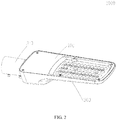
FIG. 2 is a perspective view of a lighting device at another angle according to one exemplary embodiment of the present invention; -
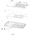
FIG. 3 is an exploded view of a lighting device according to one exemplary embodiment of the present invention; -
FIG. 4 is schematic local diagram of a light source module according to one exemplary embodiment of the present invention, the light source module in this situation including an optical element, a light emitting unit and a part of a substrate; -
FIG. 5 is a perspective view of the optical element in the light source module shown inFIG. 4 ; -
FIG. 6 is a sectional view of the light source module shown inFIG. 4 in A-A direction; -
FIG. 7 is a sectional view of the light source module shown inFIG. 4 in B-B direction; and -
FIG. 8 is a schematic comparison diagram of a light spot formed by the light source module shown inFIG. 4 with a light spot formed by the existing light distribution element. - In order to make persons skilled in the art understand technical solutions in the present invention better, the technical solutions in the embodiments of the present invention are described in detail clearly below with reference to accompanying drawings in the embodiments of the present invention. Obviously, the described embodiments are merely a part of, rather than all of, the embodiments of the present invention. Based on these embodiments of the present invention, all other embodiments that can occur to those ordinarily skilled in the art without any inventive effort shall fall into the scope of the invention.
- As shown in
FIGs. 1 and2 , thelighting device 1000 includes alight source module 100 and a power source module 200 (referring toFIG. 3 ) which are electrically connected with each other. Thepower source module 200 may obtain power from commercial power or an external battery, and then transport the power to thelight source module 100; thelight source module 100 emits light rays after obtaining the power to illuminate a preset area. - In practical applications, both the
light source module 100 and thepower source module 200 may be located on ahousing 300, thelighting device 1000 may be a street lamp or another type of a residential or outdoor lamp, and the shape and material of thehousing 300 may be determined based on the type and application environment of thelighting device 1000. For example, in a case where a street lamp is used as thelighting device 1000, thehousing 300 may also be set according to the conventional shape of the street lamp. - In the embodiments of the present invention, the lighting device further includes a vertical supporting arm (not shown), mounted to a base board, a road surface, or the like. In a case where a street lamp is used as the
lighting device 1000, this vertical supporting arm is a lamp post. Thehousing 300 includes a mountingtail end 310 for connecting the vertical supporting arm (not shown). The mountingtail end 310 may be in a shape of hollow tube, and commercial cables may be electrically connected with thelight source module 100 and thepower source module 200 through the vertical supporting arm and an interior of the mountingtail end 310. In practical use, the mountingtail end 310 may be connected with the vertical supporting arm using screws or the like. - In practical applications, a number of the
light source module 100 may be at least one; thepower source module 200 may include a current regulation unit, an overcurrent protection unit, or the like, and thepower source module 200 may be in patch or plug-in type, which is not repeated herein. - Referring to
FIG. 3 , thelight source module 100 includeslight distribution elements 10,light emitting units 20 and asubstrate 30. Thesubstrate 30 is mounted into thehousing 300, a plurality of light emittingunits 20 are arranged on thesubstrate 30 in an array, a plurality oflight distribution elements 10 are also arranged on thesubstrate 30 in an array, and each of thelight distribution elements 10 is covered on at least onelight emitting unit 20. Similarly, thelight distribution elements 10 are connected with one another by means of light transmitting materials. In practical applications, the satisfactory number oflight distribution elements 10 with desired layouts may be formed in one piece by injection moulding. - In the embodiments of the present invention, the
power source module 200 is also located on thesubstrate 30 and is electrically connected with thelight emitting unit 20 through an electrical element in thesubstrate 30. In practical applications, thesubstrate 30 includes a lengthwise direction, and a light source accommodation region 31 and a mountingregion 32 which are sequentially arranged along the lengthwise direction, and thelight emitting units 20 and thelight distribution elements 10 are all located in the light source accommodation region 31, and thepower supply module 200 is located in the mountingregion 32. - Referring to
FIGs. 4 and5 , in thelight source module 100, thelight distribution element 10 is mainly configured for regulating angle and direction of the light ray emitted from thelight emitting unit 20. Thelight distribution element 10 may be made of a transparent material, such as polycarbonate PC, polymethyl methacrylate PMMA, or the like, and the size of thelight distribution element 10 may also be adjusted adaptively according to an application scenario of thelight source module 100 and lighting demands, which are not repeated herein. - The
light distribution element 10 includes alight incident surface 11 and alight emitting surface 12 which are arranged opposite to each other. Both thelight incident surface 11 and thelight emitting surface 12 are in a shape of a smooth curved surface. That is, no obvious deformation occurs on thelight incident surface 11 and thelight emitting surface 12, and the deformation herein may refer to a protrusion, a depression, or their combination. The "obvious deformation" herein may refer to the deformation which may be recognized by human eyes or touched and perceived by fingers, or the limited lighting effect caused by the great influence of the deformation on the light ray adjustment of thelight distribution element 10, without generally referring to all types of deformations. Therefore, in a case where the deformation on thelight incident surface 11 or thelight emitting surface 12 does not affect the light distribution of thelight distribution element 10, thelight incident surface 11 or thelight emitting surface 12 may be considered as smooth; in a case where the deformation on thelight incident surface 11 or thelight emitting surface 12 cannot be recognized by human eyes or touched and perceived by fingers, thelight incident surface 11 or thelight emitting surface 12 may also be considered as smooth. - In practical applications, whether the above-mentioned deformation affects the light distribution of the
light distribution element 10 may be judged by physically or artificially comparing the light distribution element with such a deformation, with the light distribution element without such a deformation (an optimal light distribution element provided by the inventor), so as to determine whether a difference in light distribution effect therebetween is within an acceptable range. The "acceptable range" herein may be set by inventors based on the lighting scenario or user demands, without generally referring to a general standard suitable for any user or scenario. Certainly, in the case of the deformation which may be touched and perceived by fingers of a related testing personnel or seen by human eyes, thislight incident surface 11 or thelight emitting surface 12 is considered as not smooth. - In the present embodiment, the
light incident surface 11 is in a shape of an inward concave curved surface and forms anaccommodation cavity 13 for accommodating thelight emitting unit 20, the light ray emitted from thelight emitting unit 20 arrives at thelight incident surface 11, and then is emitted out through thelight emitting surface 12. Thelight emitting surface 12 is in a shape of an outward convex curved surface and protrudes in a direction the same as the direction in which thelight incident surface 11 is concaved. - In practical applications, the
light incident surface 11 and thelight emitting surface 12 are both in a shape of a partial spherical surface substantially. The "shape of partial spherical surface" herein may be obtained by cutting a whole spherical surface, or may be formed by splicing several partial spherical surfaces, so long as thelight incident surface 11 and thelight emitting surface 12 are guaranteed to be smooth. - The
light distribution element 10 may further include abottom surface 14 located at a peripheral side of thelight incident surface 11. Thebottom surface 14 is flat and is configured for being directed attached to thesubstrate 30, so as to cover thelight distribution element 10 on thelight emitting unit 20. Even if an overlarge distance exists between thelight distribution element 10 and thesubstrate 30 due to an assembly problem, the light rays can be only emitted from thelight distribution element 10, which avoids negative optical effects, such as crescent bright spots. Thelight distribution element 10 further includes atop surface 15 located at a peripheral side of thelight emitting surface 12, thetop surface 15 is arranged parallel with thebottom surface 14, and is connected with thebottom surface 14 by means of aside surface 16 to form a square mounting portion. - Certainly, in a case where the
light source module 100 includes a plurality oflight distribution elements 10, these light distribution elements may be connected with thesubstrate 30 using screws or in a snap-joint manner, or with thehousing 300, which is well-known by persons skilled in the art, and is not repeated herein. -
FIG. 6 is a sectional view of a part of the light source module shown inFIG. 4 in A-A direction. The plane where the A-A direction is located may be understood as a horizontal plane, and in this situation, thelight source module 100 is also arranged on the horizontal plane. The shapes of thelight incident surface 11 and thelight emitting surface 12 on the horizontal plane will be described in detail below with reference to the sectional view ofFIG. 6 . - The
light incident surface 11 has alight incident edge 111, thelight emitting surface 12 has alight emitting edge 121, and thelight incident edge 111 and thelight emitting edge 121 indicate the substantial shapes of thelight incident surface 11 and thelight emitting surface 12 respectively. Taking thelight incident surface 11 as an example, a profile of thelight incident edge 111 reflects a projection of thelight incident surface 11 on the horizontal plane. When thelight incident edge 111 is circular, thelight incident surface 11 is a partial spherical surface; when thelight incident edge 111 is elliptical, thelight incident surface 11 is a partial ellipsoidal surface. - In the present embodiment, a point distance between a portion of the
light incident edge 111 and a portion of thelight emitting edge 121 is less than a preset point distance threshold value which may be set in advance, for example, as 1 millimeter or other values. In practical use, the preset point distance threshold value may be set very small, such that thelight incident edge 111 and thelight emitting edge 121 are overlapped basically or exactly at some points. - Subsequently, the
light incident surface 11 and thelight emitting surface 12 both include a cross cutting line and a rip cutting line for dividing into four quadrants, wherein the cross cutting line is a cutting line in the middle along a crosswise direction of thelight incident surface 11 or thelight emitting surface 12, and the rip cutting line is a cutting line in the middle along a lengthwise direction of thelight incident surface 11 or thelight emitting surface 12. It should be noted that the cross and rip cutting lines are virtual lines for the subsequent detailed description about the technical solutions, without limiting the shapes of thelight incident surface 11 and thelight emitting surface 12. - In the present embodiment, the cut
light incident surface 11 and thelight emitting surface 12 are symmetric in the four quadrants. By taking thelight incident surface 11 which is symmetric in the four quadrants as an example, it is indicated that thelight incident surface 11 is divided into four parts after cut in crosswise and lengthwise directions, and any two of the four parts are symmetric axially or centrally. For example, the parts located in the first and second quadrants are symmetric axially, and the parts located in the first and third quadrants are symmetric centrally. - It should be noted that the "symmetric in the four quadrants" herein does not refer in particular to the absolute symmetry mathematically, but may include approximate symmetry. Still taking the
light incident surface 11 as an example, at least two of the four parts are symmetric approximately, for example, the parts in the first and second quadrants are symmetric axially approximately, or the parts in the first and third quadrants are symmetric centrally approximately, and even the parts in the first and second quadrants are symmetric axially approximately, and the parts in the first and third quadrants are symmetric centrally approximately. - In order to describe the horizontal shapes of the
light incident surface 11 and thelight emitting surface 12 conveniently, the projections of the cross and rip cutting lines, for dividing thelight incident surface 11 into four quadrants, on the horizontal plane are set to be the light incidentcross cutting line 112 and the light incidentrip cutting line 113, and the projections of the cross and rip cutting lines, for dividing thelight emitting surface 12 into four quadrants, on the horizontal plane are set to be the light emittingcross cutting line 122 and the light emittingrip cutting line 123. - In the present embodiment, a length of the light incident
cross cutting line 112 is less than that of the light incidentrip cutting line 13, i.e., the projection of thelight incident surface 11 on the horizontal plane is preferably in a shape of oval or an approximate oval. In the meantime, a length of the light emittingcross cutting line 122 is greater than that of the light emittingrip cutting line 123, i.e., the projection of thelight emitting surface 12 on the horizontal plane is preferably in a shape of oval or an approximate oval. - Preferably, a ratio between the light incident
rip cutting line 113 and the light incidentcross cutting line 112 is greater than a ratio between the light emittingrip cutting line 123 and the light emittingcross cutting line 122, such that thelight incident surface 11 is longer and narrower than thelight emitting surface 12. - The light incident
cross cutting line 112 is parallel with the light emittingcross cutting line 122. It should be noted that the parallelism herein does not refer to the absolute parallelism in the sense of data, and may also include approximate parallelism, which is not repeated herein. Moreover, the distance between the light incidentrip cutting line 113 and the light emittingrip cutting line 123 is less than a preset line distance threshold value which may be set in advance, for example, as 1 millimeter or other values. In practical use, the preset point distance threshold value may be set to be very small, such that the light incidentrip cutting line 113 and the light emittingrip cutting line 123 are overlapped basically or exactly. - The
light incident surface 11 and thelight emitting surface 12 both have center points. The center point is a middle point or a highest point of the surface. By taking thelight incident surface 11 and thelight emitting surface 12 which are both symmetric in the four quadrants as examples, the projection of the center point of thelight incident surface 11 on the horizontal plane is an intersection point between the light incidentrip cutting line 113 and the light incidentcross cutting line 112, and the projection of the center point of thelight emitting surface 12 on the horizontal plane is an intersection point between the light emittingrip cutting line 123 and the light emittingcross cutting line 122. In the present embodiment, the center point of thelight incident surface 11 and the center point of thelight emitting surface 12 are staggered with each other in a vertical direction; that is, a connection line therebetween is not along the vertical direction. - In the embodiments of the present invention, along the cross cutting line of the
light emitting surface 12, a thickness between thelight incident surface 11 and thelight emitting surface 12 is characterized in that the thickness is minimum between the center point of thelight emitting surface 12 and thelight incident surface 11, and from the center point to two sides of the light emitting surface, the thickness between the light emitting surface and the light incident surface increases symmetrically, i.e., the center point of thelight emitting surface 12 is a boundary point, and thicknesses at the two sides progressively increase at the same amplitude. -
FIG. 7 is a sectional view of a part of thelight source module 100 shown inFIG. 4 in B-B direction. The plane where the B-B direction is located may be understood as a vertical surface perpendicular to the A-A direction, at which situation, thelight distribution element 10 is still arranged on the horizontal plane. The shapes of thelight incident surface 11 and thelight emitting surface 12 on the vertical plane will be described in detail below with reference to the sectional view ofFIG. 7 . - In the present embodiment, along the rip cutting line of the
light incident surface 11, a thickness between thelight incident surface 11 and thelight emitting surface 12 is in an increasing tendency along the rip cutting line of thelight incident surface 11. - The cross sections of the
light incident surface 11 and thelight emitting surface 12 in the vertical direction are partial circles or ovals basically, and an upper edge of the cross section is a continuous arc basically. In the present embodiment, thelight incident surface 11 and thelight emitting surface 12 are both symmetric in the four quadrants, the highest point of thelight incident surface 11 is the center point of thelight incident surface 11, and the highest point of thelight emitting surface 12 is the center point of thelight emitting surface 12. - In the present embodiment, the light emitting unit 20 (referring to
FIG. 3 ) is aligned with the center point of and thelight emitting surface 12 in the vertical direction. In this situation, thelight emitting unit 20 is located on the point of intersection of the light emitting rip cutting line 123 (referring toFIG. 6 ) with the light emitting cross cutting line 122 (referring toFIG. 6 ) of thelight emitting surface 12. - It should be noted that in the embodiments of the present invention, "the
light emitting unit 20 is aligned with the center point of thelight emitting surface 12 in the vertical direction" does mean the absolute alignment mathematically, but a certain offset may occur between thelight emitting unit 20 and the center point of thelight emitting surface 12, and this offset distance between a center of thelight emitting unit 20 and the center point of thelight emitting surface 12 may be 20% of a width of thelight emitting unit 20, the offset herein may be in any direction. For example, the offset may be an offset towards one side within a range of 0.55 mm. - In a case where the
light distribution element 10 only covers onelight emitting unit 20, only the size of thelight emitting unit 20 is required to be determined. In a case where thelight emitting unit 20 is moved along the direction of the cross cutting line, the size of thelight emitting unit 20 in the direction of the cross cutting line is taken as its width. In a case where thelight distribution element 10 covers a plurality of light emittingunits 20, an overall size of theselight emitting units 20 is to be obtained, which is not repeated herein. -
FIG. 8 is a schematic comparison diagram of a light spot formed by the light source module shown inFIG. 4 with a light spot formed by the existing light distribution element. Referring toFIG. 5 , the light rays emitted from thelight emitting unit 20 are processed by thelight incident surface 11 and thelight emitting surface 12, and then shift away from the center point of thelight incident surface 11, that is to shift towards a portion of the light distribution element with a larger thickness, such that the light rays are diffused, thereby obtaining alight spot 400, and a width of an area of ayellow spot 410 in thelight spot 400 is enlarged. Compared with the width of theyellow spot 510 in thelight spot 500 of the light ray emitted from an ordinary light distribution element, the area of theyellow spot 410 formed by thelight distribution element 10 is obviously larger, such that the concentration of the yellow light ray is reduced, thereby weakening the yellow spot. - In the embodiments of the present invention, in the light spot formed by an area of the
light distribution element 10 with a larger thickness, a color tolerance between the yellow spot and white light is less than a preset color difference. The preset color tolerance may be set according to the reception capability or ethnic characteristics of the user in the application area of the lighting device 1000 (referring toFIG. 2 ), so as to ensure that the yellow spot formed in the area of thelight distribution element 10 with a larger thickness is light enough within the acceptable range of the user. In practical applications, the preset color difference is 4. - Each embodiment in the specification is described in a progressive manner. The same or similar parts in the embodiments are just references to each other. Every embodiment illustrates in emphasis what is different from the other embodiments. In particular, for the apparatus embodiment, because it is basically similar to the method embodiment, the description is relatively simple, and for the relevant part, reference is just made to the part of the description of the method embodiment.
- What are described above are only exemplary embodiments of the present invention, but are not intended to limit the protection scope of the present invention. Persons of ordinary skill in the art may make kinds of modifications to the present invention. Any modification, equivalent replacement, and improvement made within the spirit and principle of the present invention all fall within the protection scope of the present invention.
Claims (28)
- A light distribution element, comprising:a light incident surface, which is in a shape of a smooth inward concave curved surface and forms an accommodation cavity for accommodating a light emitting unit; anda light emitting surface, which is in a shape of a smooth outward convex curved surface and is opposite to the light incident surface,wherein a thickness difference is between the light incident surface and the light emitting surface, andin a light spot formed by light emitted from the light emitting surface located on a portion with a larger thickness, a color tolerance between a yellow spot and white light is less than a preset color difference.
- The light distribution element according to claim 1, wherein the preset color difference is 4.
- The light distribution element according to claim 1, wherein an offset distance between a center of the light emitting unit and a center point of the light emitting surface is 20% of a width of the light emitting unit.
- The light distribution element according to claim 1, wherein an offset distance between a center of the light emitting unit and a center point of the light emitting surface is within a range of 0.55 mm.
- The light distribution element according to claim 1, wherein the light emitting surface comprises a center point, the center point of the light emitting surface is staggered with a center point of the light incident surface in a vertical direction.
- A light distribution element, comprising:a light incident surface, which is in a shape of a smooth inward concave curved surface and forms an accommodation cavity for accommodating a light emitting unit, and comprises a center point; anda light emitting surface, which is in a shape of a smooth outward convex curved surface and is opposite to the light incident surface, and comprises a center point,wherein the center point of the light emitting surface is staggered with the center point of the light incident surface in a vertical direction, and the center point of the light emitting surface is aligned with the light emitting unit located in the accommodation cavity in the vertical direction.
- The light distribution element according to claim 6, wherein the center point of the light incident surface is a highest point of the light incident surface, and the center point of the light emitting surface is a highest point of the light emitting surface.
- The light distribution element according to claim 1 or claim 6, wherein each of the light incident surface and the light emitting surface has a cross cutting line and a rip cutting line for dividing into four quadrants, and both the light incident surface and the light emitting surface are symmetric in the four quadrants.
- The light distribution element according to claim 8, wherein along the cross cutting line of the light emitting surface, a thickness between the light incident surface and the light emitting surface is characterized in that the thickness is minimum between the center point of the light emitting surface and the light incident surface, and from the center point to two sides of the light emitting surface, the thickness between the light emitting surface and the light incident surface increases symmetrically.
- The light distribution element according to claim 8, wherein along the rip cutting line of the light incident surface, a thickness between the light incident surface and the light emitting surface is in an increasing tendency.
- The light distribution element according to claim 8, wherein a projection of the cross cutting line of the light incident surface on a horizontal plane is shorter than a projection of the rip cutting line of the light incident surface on the horizontal plane.
- The light distribution element according to claim 8, wherein a projection of the cross cutting line of the light emitting surface on a horizontal plane is longer than a projection of the rip cutting line of the light emitting surface on the horizontal plane.
- The light distribution element according to claim 8, wherein a projection of the cross cutting line of the light incident surface on a horizontal plane is parallel to a projection of the cross cutting line of the light emitting surface on the horizontal plane.
- The light distribution element according to claim 8, wherein a distance between a projection of the rip cutting line of the light incident surface on a horizontal plane and a projection of the rip cutting line of the light emitting surface on the horizontal plane is less than a preset line distance threshold value.
- The light distribution element according to claim 14, wherein the projection of the rip cutting line of the light incident surface on the horizontal plane coincides with the projection of the rip cutting line of the light emitting surface on the horizontal plane.
- The light distribution element according to claim 8, wherein a ratio between a projection of the cross cutting line and a projection of the rip cutting line on a horizontal plane in the light incident surface is greater than a ratio between a projection of the cross cutting line and a projection of the rip cutting line on the horizontal plane of the light emitting surface.
- The light distribution element according to claim 1 or claim 6, wherein in projections on a horizontal plane, a point distance between a portion of an edge of the light incident surface and a portion of an edge of the light emitting surface is less than a preset point distance threshold value.
- The light distribution element according to claim 17, wherein in the projections of the light incident surface and the light emitting surface on the horizontal plane, at least a part of the edge of the light incident surface coincides with a part of the edge of the light emitting surface.
- The light distribution element according to claim 1 or claim 6, wherein the light distribution element comprises a bottom surface surrounding a peripheral side of the light incident surface and the bottom surface is flat.
- The light distribution element according to claim 19, wherein the light distribution element comprises a top surface surrounding a peripheral side of the light emitting surface, and the bottom surface and the top surface are disposed in parallel and are connected with each other by a side surface to form a mounting part.
- A light source module, comprising:a substrate,a light emitting unit, provided on the substrate, andthe light distribution element according to any one of claims 1- 20,wherein the light distribution element is mounted to the substrate and covers the light emitting unit, and the light emitting unit is located in the accommodation cavity of the light distribution element and is aligned with a center point of the light emitting surface in a vertical direction.
- The light source module according to claim 21, wherein the light source module comprises a plurality of light distribution elements and a plurality of light emitting units, the plurality of light emitting units are arranged on the substrate in an array, and at least one light emitting unit is provide within each of the plurality of light distribution elements.
- The light source module according to claim 21, wherein an offset direction of a center point of the light incident surface is identical to an offset direction of the center point of the light emitting surface in each light distribution element.
- The light source module according to claim 21, wherein a distance between the light distribution elements in a same row or a same column is same.
- The light source module according to claim 21, wherein the substrate comprises a lengthwise direction, the substrate comprises a light source accommodation region and a mounting region which are sequentially arranged along the lengthwise direction, and the light emitting unit is in the light source accommodation region.
- A lighting device, comprising:a power source module, andat least one light source module according to claim 21,wherein the light source module is electrically connected with the power source module.
- The lighting device according to claim 26, wherein the lighting device is a street lamp.
- The lighting device according to claim 26, wherein the lighting device further comprises a housing, and the power source module and the light source module are mounted to the housing;
the lighting device further comprises a vertical supporting arm connected with the housing.
Applications Claiming Priority (5)
| Application Number | Priority Date | Filing Date | Title |
|---|---|---|---|
| CN201720614705.1U CN207778237U (en) | 2017-05-27 | 2017-05-27 | Light distribution element, light source module group and lighting device |
| CN201710396648.9A CN107023787A (en) | 2017-05-27 | 2017-05-27 | light distribution element, light source module and lighting device |
| CN201710395774.2A CN107023786A (en) | 2017-05-27 | 2017-05-27 | light distribution element, light source module and lighting device |
| CN201720614456.6U CN207378677U (en) | 2017-05-27 | 2017-05-27 | Light distribution element, light source module group and lighting device |
| PCT/CN2018/088230 WO2018219211A1 (en) | 2017-05-27 | 2018-05-24 | Light distribution element, light source module and lighting device |
Publications (3)
| Publication Number | Publication Date |
|---|---|
| EP3564579A1 true EP3564579A1 (en) | 2019-11-06 |
| EP3564579A4 EP3564579A4 (en) | 2020-07-01 |
| EP3564579B1 EP3564579B1 (en) | 2023-08-16 |
Family
ID=64455173
Family Applications (1)
| Application Number | Title | Priority Date | Filing Date |
|---|---|---|---|
| EP18808896.7A Active EP3564579B1 (en) | 2017-05-27 | 2018-05-24 | Light distribution element, light source module and lighting device |
Country Status (3)
| Country | Link |
|---|---|
| US (1) | US10928034B2 (en) |
| EP (1) | EP3564579B1 (en) |
| WO (1) | WO2018219211A1 (en) |
Families Citing this family (1)
| Publication number | Priority date | Publication date | Assignee | Title |
|---|---|---|---|---|
| USD1083187S1 (en) * | 2023-09-11 | 2025-07-08 | Zhongshan Yinghao Solar Technology Co., Ltd. | Solar street light |
Family Cites Families (20)
| Publication number | Priority date | Publication date | Assignee | Title |
|---|---|---|---|---|
| TWI336386B (en) * | 2008-03-07 | 2011-01-21 | Ind Tech Res Inst | Illumination device |
| JP5565952B2 (en) * | 2010-08-25 | 2014-08-06 | パナソニック株式会社 | lighting equipment |
| US20120307495A1 (en) * | 2011-06-06 | 2012-12-06 | Leotek Electronics Corporation | Optical lens and optical lens plate |
| CN202165991U (en) * | 2011-08-02 | 2012-03-14 | 海洋王照明科技股份有限公司 | Lens and LED lamp |
| US8702278B2 (en) * | 2011-12-15 | 2014-04-22 | Tsmc Solid State Lighting Ltd. | LED lighting apparatus with flexible light modules |
| CN104344335A (en) * | 2013-08-05 | 2015-02-11 | 鸿富锦精密工业(深圳)有限公司 | Lens and light source module using the lens |
| US9175832B2 (en) * | 2013-09-16 | 2015-11-03 | Light Engine Limited | Faceted LED street lamp lens |
| CN203628520U (en) * | 2013-10-30 | 2014-06-04 | 广东德豪润达电气股份有限公司 | Light distribution lens and LED garden lamp with the light distribution lens |
| CN203784827U (en) * | 2013-11-25 | 2014-08-20 | 东莞市欧科光电科技有限公司 | Novel LED lens for backlight of liquid crystal display |
| US9835317B2 (en) * | 2014-03-15 | 2017-12-05 | Cree, Inc. | Luminaire utilizing waveguide |
| US10317608B2 (en) * | 2014-03-15 | 2019-06-11 | Cree, Inc. | Luminaires utilizing optical waveguide |
| CN105276522B (en) * | 2014-06-30 | 2019-04-30 | 欧普照明股份有限公司 | A polarized lens for LED lamps and LED lamps with the same |
| CN204494304U (en) * | 2015-02-17 | 2015-07-22 | 宁波石上光电科技有限公司 | A kind of light-distribution lens for power type LED lamp |
| JP6534065B2 (en) * | 2015-07-28 | 2019-06-26 | パナソニックIpマネジメント株式会社 | Optical lens, lens array and lighting apparatus |
| CN207146077U (en) * | 2017-05-25 | 2018-03-27 | 欧普照明股份有限公司 | A kind of light fixture |
| CN207378677U (en) * | 2017-05-27 | 2018-05-18 | 欧普照明股份有限公司 | Light distribution element, light source module group and lighting device |
| CN107023786A (en) * | 2017-05-27 | 2017-08-08 | 欧普照明股份有限公司 | light distribution element, light source module and lighting device |
| CN107023787A (en) * | 2017-05-27 | 2017-08-08 | 欧普照明股份有限公司 | light distribution element, light source module and lighting device |
| USD859731S1 (en) * | 2017-08-22 | 2019-09-10 | Opple Lighting Co., Ltd. | Light |
| EP3690311B1 (en) * | 2017-09-28 | 2024-12-04 | Suzhou Opple Lighting Co., Ltd. | Lighting device |
-
2018
- 2018-05-24 EP EP18808896.7A patent/EP3564579B1/en active Active
- 2018-05-24 WO PCT/CN2018/088230 patent/WO2018219211A1/en not_active Ceased
-
2019
- 2019-11-26 US US16/697,166 patent/US10928034B2/en active Active
Also Published As
| Publication number | Publication date |
|---|---|
| EP3564579A4 (en) | 2020-07-01 |
| EP3564579B1 (en) | 2023-08-16 |
| US10928034B2 (en) | 2021-02-23 |
| US20200096174A1 (en) | 2020-03-26 |
| WO2018219211A1 (en) | 2018-12-06 |
Similar Documents
| Publication | Publication Date | Title |
|---|---|---|
| US7866837B2 (en) | Skew light illumination lens device | |
| CN105202482B (en) | Lens and lighting device | |
| KR20090081395A (en) | Lighting device with cover layer | |
| US10400992B2 (en) | Lighting apparatus having different reflection sheets | |
| EP2869107A1 (en) | Lens, led module and illumination system having same | |
| US20040125588A1 (en) | Front light module | |
| KR101419031B1 (en) | Light emitting device and lighting device having the same | |
| CN105222086B (en) | Secondary optical element and light source module | |
| US20250004331A1 (en) | Front light source and display device | |
| EP3564579B1 (en) | Light distribution element, light source module and lighting device | |
| CN114719226B (en) | Lens strip, grading lens, bar lamp and road lighting device | |
| CN107023787A (en) | light distribution element, light source module and lighting device | |
| CN107023786A (en) | light distribution element, light source module and lighting device | |
| CN207378677U (en) | Light distribution element, light source module group and lighting device | |
| KR20220098713A (en) | Lighting apparatus | |
| CN105953175B (en) | Projecting lamp lens, have light-emitting module and projecting lamp of this projecting lamp lens | |
| US10190730B2 (en) | Light flux controlling member, light emitting device and illuminating device | |
| US10215350B2 (en) | Luminaire, especially for road lighting | |
| US11982438B2 (en) | Uniform illumination lens and lamp thereof | |
| CN220119222U (en) | Lighting lamp | |
| US20060202218A1 (en) | Light-emitting diode for decoration | |
| CN207778237U (en) | Light distribution element, light source module group and lighting device | |
| US10295732B2 (en) | Light guide plate, backlight module and display module | |
| JP6751452B2 (en) | Area lighting device | |
| US10788169B2 (en) | Lighting device |
Legal Events
| Date | Code | Title | Description |
|---|---|---|---|
| STAA | Information on the status of an ep patent application or granted ep patent |
Free format text: STATUS: THE INTERNATIONAL PUBLICATION HAS BEEN MADE |
|
| PUAI | Public reference made under article 153(3) epc to a published international application that has entered the european phase |
Free format text: ORIGINAL CODE: 0009012 |
|
| STAA | Information on the status of an ep patent application or granted ep patent |
Free format text: STATUS: REQUEST FOR EXAMINATION WAS MADE |
|
| 17P | Request for examination filed |
Effective date: 20190801 |
|
| AK | Designated contracting states |
Kind code of ref document: A1 Designated state(s): AL AT BE BG CH CY CZ DE DK EE ES FI FR GB GR HR HU IE IS IT LI LT LU LV MC MK MT NL NO PL PT RO RS SE SI SK SM TR |
|
| AX | Request for extension of the european patent |
Extension state: BA ME |
|
| A4 | Supplementary search report drawn up and despatched |
Effective date: 20200604 |
|
| RIC1 | Information provided on ipc code assigned before grant |
Ipc: F21W 131/103 20060101ALN20200528BHEP Ipc: F21V 5/04 20060101AFI20200528BHEP Ipc: F21W 131/10 20060101ALN20200528BHEP Ipc: F21V 5/00 20180101ALI20200528BHEP Ipc: F21V 5/08 20060101ALI20200528BHEP Ipc: F21Y 105/16 20160101ALN20200528BHEP Ipc: F21Y 115/10 20160101ALN20200528BHEP |
|
| RIC1 | Information provided on ipc code assigned before grant |
Ipc: F21Y 115/10 20160101ALN20200617BHEP Ipc: F21V 5/00 20180101ALI20200617BHEP Ipc: F21W 131/10 20060101ALN20200617BHEP Ipc: F21V 5/04 20060101AFI20200617BHEP Ipc: F21W 131/103 20060101ALN20200617BHEP Ipc: F21Y 105/16 20160101ALN20200617BHEP Ipc: F21V 5/08 20060101ALI20200617BHEP |
|
| DAV | Request for validation of the european patent (deleted) | ||
| DAX | Request for extension of the european patent (deleted) | ||
| STAA | Information on the status of an ep patent application or granted ep patent |
Free format text: STATUS: EXAMINATION IS IN PROGRESS |
|
| 17Q | First examination report despatched |
Effective date: 20201203 |
|
| GRAP | Despatch of communication of intention to grant a patent |
Free format text: ORIGINAL CODE: EPIDOSNIGR1 |
|
| STAA | Information on the status of an ep patent application or granted ep patent |
Free format text: STATUS: GRANT OF PATENT IS INTENDED |
|
| RIC1 | Information provided on ipc code assigned before grant |
Ipc: F21W 131/103 20060101ALN20230206BHEP Ipc: F21Y 105/16 20160101ALN20230206BHEP Ipc: F21Y 115/10 20160101ALN20230206BHEP Ipc: F21W 131/10 20060101ALN20230206BHEP Ipc: F21V 5/00 20060101ALI20230206BHEP Ipc: F21V 5/08 20060101ALI20230206BHEP Ipc: F21V 5/04 20060101AFI20230206BHEP |
|
| RIC1 | Information provided on ipc code assigned before grant |
Ipc: F21W 131/103 20060101ALN20230216BHEP Ipc: F21Y 105/16 20160101ALN20230216BHEP Ipc: F21Y 115/10 20160101ALN20230216BHEP Ipc: F21W 131/10 20060101ALN20230216BHEP Ipc: F21V 5/00 20060101ALI20230216BHEP Ipc: F21V 5/08 20060101ALI20230216BHEP Ipc: F21V 5/04 20060101AFI20230216BHEP |
|
| INTG | Intention to grant announced |
Effective date: 20230313 |
|
| GRAS | Grant fee paid |
Free format text: ORIGINAL CODE: EPIDOSNIGR3 |
|
| GRAA | (expected) grant |
Free format text: ORIGINAL CODE: 0009210 |
|
| STAA | Information on the status of an ep patent application or granted ep patent |
Free format text: STATUS: THE PATENT HAS BEEN GRANTED |
|
| AK | Designated contracting states |
Kind code of ref document: B1 Designated state(s): AL AT BE BG CH CY CZ DE DK EE ES FI FR GB GR HR HU IE IS IT LI LT LU LV MC MK MT NL NO PL PT RO RS SE SI SK SM TR |
|
| REG | Reference to a national code |
Ref country code: CH Ref legal event code: EP Ref country code: DE Ref legal event code: R096 Ref document number: 602018055564 Country of ref document: DE |
|
| REG | Reference to a national code |
Ref country code: NL Ref legal event code: FP |
|
| REG | Reference to a national code |
Ref country code: IE Ref legal event code: FG4D |
|
| REG | Reference to a national code |
Ref country code: LT Ref legal event code: MG9D |
|
| REG | Reference to a national code |
Ref country code: AT Ref legal event code: MK05 Ref document number: 1600379 Country of ref document: AT Kind code of ref document: T Effective date: 20230816 |
|
| PG25 | Lapsed in a contracting state [announced via postgrant information from national office to epo] |
Ref country code: GR Free format text: LAPSE BECAUSE OF FAILURE TO SUBMIT A TRANSLATION OF THE DESCRIPTION OR TO PAY THE FEE WITHIN THE PRESCRIBED TIME-LIMIT Effective date: 20231117 |
|
| PG25 | Lapsed in a contracting state [announced via postgrant information from national office to epo] |
Ref country code: IS Free format text: LAPSE BECAUSE OF FAILURE TO SUBMIT A TRANSLATION OF THE DESCRIPTION OR TO PAY THE FEE WITHIN THE PRESCRIBED TIME-LIMIT Effective date: 20231216 |
|
| PG25 | Lapsed in a contracting state [announced via postgrant information from national office to epo] |
Ref country code: SE Free format text: LAPSE BECAUSE OF FAILURE TO SUBMIT A TRANSLATION OF THE DESCRIPTION OR TO PAY THE FEE WITHIN THE PRESCRIBED TIME-LIMIT Effective date: 20230816 Ref country code: RS Free format text: LAPSE BECAUSE OF FAILURE TO SUBMIT A TRANSLATION OF THE DESCRIPTION OR TO PAY THE FEE WITHIN THE PRESCRIBED TIME-LIMIT Effective date: 20230816 Ref country code: PT Free format text: LAPSE BECAUSE OF FAILURE TO SUBMIT A TRANSLATION OF THE DESCRIPTION OR TO PAY THE FEE WITHIN THE PRESCRIBED TIME-LIMIT Effective date: 20231218 Ref country code: NO Free format text: LAPSE BECAUSE OF FAILURE TO SUBMIT A TRANSLATION OF THE DESCRIPTION OR TO PAY THE FEE WITHIN THE PRESCRIBED TIME-LIMIT Effective date: 20231116 Ref country code: LV Free format text: LAPSE BECAUSE OF FAILURE TO SUBMIT A TRANSLATION OF THE DESCRIPTION OR TO PAY THE FEE WITHIN THE PRESCRIBED TIME-LIMIT Effective date: 20230816 Ref country code: LT Free format text: LAPSE BECAUSE OF FAILURE TO SUBMIT A TRANSLATION OF THE DESCRIPTION OR TO PAY THE FEE WITHIN THE PRESCRIBED TIME-LIMIT Effective date: 20230816 Ref country code: IS Free format text: LAPSE BECAUSE OF FAILURE TO SUBMIT A TRANSLATION OF THE DESCRIPTION OR TO PAY THE FEE WITHIN THE PRESCRIBED TIME-LIMIT Effective date: 20231216 Ref country code: HR Free format text: LAPSE BECAUSE OF FAILURE TO SUBMIT A TRANSLATION OF THE DESCRIPTION OR TO PAY THE FEE WITHIN THE PRESCRIBED TIME-LIMIT Effective date: 20230816 Ref country code: GR Free format text: LAPSE BECAUSE OF FAILURE TO SUBMIT A TRANSLATION OF THE DESCRIPTION OR TO PAY THE FEE WITHIN THE PRESCRIBED TIME-LIMIT Effective date: 20231117 Ref country code: FI Free format text: LAPSE BECAUSE OF FAILURE TO SUBMIT A TRANSLATION OF THE DESCRIPTION OR TO PAY THE FEE WITHIN THE PRESCRIBED TIME-LIMIT Effective date: 20230816 Ref country code: AT Free format text: LAPSE BECAUSE OF FAILURE TO SUBMIT A TRANSLATION OF THE DESCRIPTION OR TO PAY THE FEE WITHIN THE PRESCRIBED TIME-LIMIT Effective date: 20230816 |
|
| PG25 | Lapsed in a contracting state [announced via postgrant information from national office to epo] |
Ref country code: PL Free format text: LAPSE BECAUSE OF FAILURE TO SUBMIT A TRANSLATION OF THE DESCRIPTION OR TO PAY THE FEE WITHIN THE PRESCRIBED TIME-LIMIT Effective date: 20230816 |
|
| PG25 | Lapsed in a contracting state [announced via postgrant information from national office to epo] |
Ref country code: ES Free format text: LAPSE BECAUSE OF FAILURE TO SUBMIT A TRANSLATION OF THE DESCRIPTION OR TO PAY THE FEE WITHIN THE PRESCRIBED TIME-LIMIT Effective date: 20230816 |
|
| PG25 | Lapsed in a contracting state [announced via postgrant information from national office to epo] |
Ref country code: SM Free format text: LAPSE BECAUSE OF FAILURE TO SUBMIT A TRANSLATION OF THE DESCRIPTION OR TO PAY THE FEE WITHIN THE PRESCRIBED TIME-LIMIT Effective date: 20230816 Ref country code: RO Free format text: LAPSE BECAUSE OF FAILURE TO SUBMIT A TRANSLATION OF THE DESCRIPTION OR TO PAY THE FEE WITHIN THE PRESCRIBED TIME-LIMIT Effective date: 20230816 Ref country code: ES Free format text: LAPSE BECAUSE OF FAILURE TO SUBMIT A TRANSLATION OF THE DESCRIPTION OR TO PAY THE FEE WITHIN THE PRESCRIBED TIME-LIMIT Effective date: 20230816 Ref country code: EE Free format text: LAPSE BECAUSE OF FAILURE TO SUBMIT A TRANSLATION OF THE DESCRIPTION OR TO PAY THE FEE WITHIN THE PRESCRIBED TIME-LIMIT Effective date: 20230816 Ref country code: DK Free format text: LAPSE BECAUSE OF FAILURE TO SUBMIT A TRANSLATION OF THE DESCRIPTION OR TO PAY THE FEE WITHIN THE PRESCRIBED TIME-LIMIT Effective date: 20230816 Ref country code: CZ Free format text: LAPSE BECAUSE OF FAILURE TO SUBMIT A TRANSLATION OF THE DESCRIPTION OR TO PAY THE FEE WITHIN THE PRESCRIBED TIME-LIMIT Effective date: 20230816 Ref country code: SK Free format text: LAPSE BECAUSE OF FAILURE TO SUBMIT A TRANSLATION OF THE DESCRIPTION OR TO PAY THE FEE WITHIN THE PRESCRIBED TIME-LIMIT Effective date: 20230816 |
|
| REG | Reference to a national code |
Ref country code: DE Ref legal event code: R097 Ref document number: 602018055564 Country of ref document: DE |
|
| PLBE | No opposition filed within time limit |
Free format text: ORIGINAL CODE: 0009261 |
|
| STAA | Information on the status of an ep patent application or granted ep patent |
Free format text: STATUS: NO OPPOSITION FILED WITHIN TIME LIMIT |
|
| 26N | No opposition filed |
Effective date: 20240517 |
|
| PG25 | Lapsed in a contracting state [announced via postgrant information from national office to epo] |
Ref country code: IT Free format text: LAPSE BECAUSE OF FAILURE TO SUBMIT A TRANSLATION OF THE DESCRIPTION OR TO PAY THE FEE WITHIN THE PRESCRIBED TIME-LIMIT Effective date: 20230816 Ref country code: SI Free format text: LAPSE BECAUSE OF FAILURE TO SUBMIT A TRANSLATION OF THE DESCRIPTION OR TO PAY THE FEE WITHIN THE PRESCRIBED TIME-LIMIT Effective date: 20230816 |
|
| PGFP | Annual fee paid to national office [announced via postgrant information from national office to epo] |
Ref country code: FR Payment date: 20240524 Year of fee payment: 7 |
|
| PGFP | Annual fee paid to national office [announced via postgrant information from national office to epo] |
Ref country code: BE Payment date: 20240515 Year of fee payment: 7 |
|
| PG25 | Lapsed in a contracting state [announced via postgrant information from national office to epo] |
Ref country code: BG Free format text: LAPSE BECAUSE OF FAILURE TO SUBMIT A TRANSLATION OF THE DESCRIPTION OR TO PAY THE FEE WITHIN THE PRESCRIBED TIME-LIMIT Effective date: 20230816 |
|
| PG25 | Lapsed in a contracting state [announced via postgrant information from national office to epo] |
Ref country code: BG Free format text: LAPSE BECAUSE OF FAILURE TO SUBMIT A TRANSLATION OF THE DESCRIPTION OR TO PAY THE FEE WITHIN THE PRESCRIBED TIME-LIMIT Effective date: 20230816 |
|
| REG | Reference to a national code |
Ref country code: CH Ref legal event code: PL |
|
| PG25 | Lapsed in a contracting state [announced via postgrant information from national office to epo] |
Ref country code: MC Free format text: LAPSE BECAUSE OF FAILURE TO SUBMIT A TRANSLATION OF THE DESCRIPTION OR TO PAY THE FEE WITHIN THE PRESCRIBED TIME-LIMIT Effective date: 20230816 |
|
| PG25 | Lapsed in a contracting state [announced via postgrant information from national office to epo] |
Ref country code: LU Free format text: LAPSE BECAUSE OF NON-PAYMENT OF DUE FEES Effective date: 20240524 |
|
| PG25 | Lapsed in a contracting state [announced via postgrant information from national office to epo] |
Ref country code: MC Free format text: LAPSE BECAUSE OF FAILURE TO SUBMIT A TRANSLATION OF THE DESCRIPTION OR TO PAY THE FEE WITHIN THE PRESCRIBED TIME-LIMIT Effective date: 20230816 Ref country code: LU Free format text: LAPSE BECAUSE OF NON-PAYMENT OF DUE FEES Effective date: 20240524 Ref country code: CH Free format text: LAPSE BECAUSE OF NON-PAYMENT OF DUE FEES Effective date: 20240531 |
|
| PG25 | Lapsed in a contracting state [announced via postgrant information from national office to epo] |
Ref country code: IE Free format text: LAPSE BECAUSE OF NON-PAYMENT OF DUE FEES Effective date: 20240524 |
|
| PGFP | Annual fee paid to national office [announced via postgrant information from national office to epo] |
Ref country code: NL Payment date: 20250429 Year of fee payment: 8 |
|
| PGFP | Annual fee paid to national office [announced via postgrant information from national office to epo] |
Ref country code: DE Payment date: 20250513 Year of fee payment: 8 |
|
| PGFP | Annual fee paid to national office [announced via postgrant information from national office to epo] |
Ref country code: GB Payment date: 20250521 Year of fee payment: 8 |
|
| PG25 | Lapsed in a contracting state [announced via postgrant information from national office to epo] |
Ref country code: CY Free format text: LAPSE BECAUSE OF FAILURE TO SUBMIT A TRANSLATION OF THE DESCRIPTION OR TO PAY THE FEE WITHIN THE PRESCRIBED TIME-LIMIT; INVALID AB INITIO Effective date: 20180524 |
|
| PG25 | Lapsed in a contracting state [announced via postgrant information from national office to epo] |
Ref country code: HU Free format text: LAPSE BECAUSE OF FAILURE TO SUBMIT A TRANSLATION OF THE DESCRIPTION OR TO PAY THE FEE WITHIN THE PRESCRIBED TIME-LIMIT; INVALID AB INITIO Effective date: 20180524 |
|
| REG | Reference to a national code |
Ref country code: BE Ref legal event code: MM Effective date: 20250531 |
|
| PG25 | Lapsed in a contracting state [announced via postgrant information from national office to epo] |
Ref country code: BE Free format text: LAPSE BECAUSE OF NON-PAYMENT OF DUE FEES Effective date: 20250531 |
|
| PG25 | Lapsed in a contracting state [announced via postgrant information from national office to epo] |
Ref country code: FR Free format text: LAPSE BECAUSE OF NON-PAYMENT OF DUE FEES Effective date: 20250531 |