EP3561951A1 - Unit cell antenna for phased arrays - Google Patents
Unit cell antenna for phased arrays Download PDFInfo
- Publication number
- EP3561951A1 EP3561951A1 EP19170534.2A EP19170534A EP3561951A1 EP 3561951 A1 EP3561951 A1 EP 3561951A1 EP 19170534 A EP19170534 A EP 19170534A EP 3561951 A1 EP3561951 A1 EP 3561951A1
- Authority
- EP
- European Patent Office
- Prior art keywords
- antenna
- dipole
- dipole antenna
- pcb
- phased array
- Prior art date
- Legal status (The legal status is an assumption and is not a legal conclusion. Google has not performed a legal analysis and makes no representation as to the accuracy of the status listed.)
- Granted
Links
Images






Classifications
-
- G—PHYSICS
- G01—MEASURING; TESTING
- G01S—RADIO DIRECTION-FINDING; RADIO NAVIGATION; DETERMINING DISTANCE OR VELOCITY BY USE OF RADIO WAVES; LOCATING OR PRESENCE-DETECTING BY USE OF THE REFLECTION OR RERADIATION OF RADIO WAVES; ANALOGOUS ARRANGEMENTS USING OTHER WAVES
- G01S13/00—Systems using the reflection or reradiation of radio waves, e.g. radar systems; Analogous systems using reflection or reradiation of waves whose nature or wavelength is irrelevant or unspecified
- G01S13/02—Systems using reflection of radio waves, e.g. primary radar systems; Analogous systems
-
- H—ELECTRICITY
- H01—ELECTRIC ELEMENTS
- H01Q—ANTENNAS, i.e. RADIO AERIALS
- H01Q1/00—Details of, or arrangements associated with, antennas
- H01Q1/27—Adaptation for use in or on movable bodies
- H01Q1/28—Adaptation for use in or on aircraft, missiles, satellites, or balloons
-
- H—ELECTRICITY
- H01—ELECTRIC ELEMENTS
- H01Q—ANTENNAS, i.e. RADIO AERIALS
- H01Q1/00—Details of, or arrangements associated with, antennas
- H01Q1/27—Adaptation for use in or on movable bodies
- H01Q1/28—Adaptation for use in or on aircraft, missiles, satellites, or balloons
- H01Q1/285—Aircraft wire antennas
-
- H—ELECTRICITY
- H01—ELECTRIC ELEMENTS
- H01Q—ANTENNAS, i.e. RADIO AERIALS
- H01Q1/00—Details of, or arrangements associated with, antennas
- H01Q1/27—Adaptation for use in or on movable bodies
- H01Q1/28—Adaptation for use in or on aircraft, missiles, satellites, or balloons
- H01Q1/286—Adaptation for use in or on aircraft, missiles, satellites, or balloons substantially flush mounted with the skin of the craft
-
- H—ELECTRICITY
- H01—ELECTRIC ELEMENTS
- H01Q—ANTENNAS, i.e. RADIO AERIALS
- H01Q1/00—Details of, or arrangements associated with, antennas
- H01Q1/27—Adaptation for use in or on movable bodies
- H01Q1/28—Adaptation for use in or on aircraft, missiles, satellites, or balloons
- H01Q1/288—Satellite antennas
-
- H—ELECTRICITY
- H01—ELECTRIC ELEMENTS
- H01Q—ANTENNAS, i.e. RADIO AERIALS
- H01Q1/00—Details of, or arrangements associated with, antennas
- H01Q1/36—Structural form of radiating elements, e.g. cone, spiral, umbrella; Particular materials used therewith
- H01Q1/38—Structural form of radiating elements, e.g. cone, spiral, umbrella; Particular materials used therewith formed by a conductive layer on an insulating support
-
- H—ELECTRICITY
- H01—ELECTRIC ELEMENTS
- H01Q—ANTENNAS, i.e. RADIO AERIALS
- H01Q1/00—Details of, or arrangements associated with, antennas
- H01Q1/50—Structural association of antennas with earthing switches, lead-in devices or lightning protectors
-
- H—ELECTRICITY
- H01—ELECTRIC ELEMENTS
- H01Q—ANTENNAS, i.e. RADIO AERIALS
- H01Q21/00—Antenna arrays or systems
- H01Q21/0006—Particular feeding systems
- H01Q21/0025—Modular arrays
-
- H—ELECTRICITY
- H01—ELECTRIC ELEMENTS
- H01Q—ANTENNAS, i.e. RADIO AERIALS
- H01Q21/00—Antenna arrays or systems
- H01Q21/0087—Apparatus or processes specially adapted for manufacturing antenna arrays
-
- H—ELECTRICITY
- H01—ELECTRIC ELEMENTS
- H01Q—ANTENNAS, i.e. RADIO AERIALS
- H01Q21/00—Antenna arrays or systems
- H01Q21/06—Arrays of individually energised antenna units similarly polarised and spaced apart
- H01Q21/061—Two dimensional planar arrays
- H01Q21/062—Two dimensional planar arrays using dipole aerials
-
- H—ELECTRICITY
- H01—ELECTRIC ELEMENTS
- H01Q—ANTENNAS, i.e. RADIO AERIALS
- H01Q21/00—Antenna arrays or systems
- H01Q21/06—Arrays of individually energised antenna units similarly polarised and spaced apart
- H01Q21/061—Two dimensional planar arrays
- H01Q21/065—Patch antenna array
-
- H—ELECTRICITY
- H01—ELECTRIC ELEMENTS
- H01Q—ANTENNAS, i.e. RADIO AERIALS
- H01Q21/00—Antenna arrays or systems
- H01Q21/06—Arrays of individually energised antenna units similarly polarised and spaced apart
- H01Q21/22—Antenna units of the array energised non-uniformly in amplitude or phase, e.g. tapered array or binomial array
-
- H—ELECTRICITY
- H01—ELECTRIC ELEMENTS
- H01Q—ANTENNAS, i.e. RADIO AERIALS
- H01Q9/00—Electrically-short antennas having dimensions not more than twice the operating wavelength and consisting of conductive active radiating elements
- H01Q9/04—Resonant antennas
- H01Q9/16—Resonant antennas with feed intermediate between the extremities of the antenna, e.g. centre-fed dipole
- H01Q9/28—Conical, cylindrical, cage, strip, gauze, or like elements having an extended radiating surface; Elements comprising two conical surfaces having collinear axes and adjacent apices and fed by two-conductor transmission lines
- H01Q9/285—Planar dipole
-
- G—PHYSICS
- G01—MEASURING; TESTING
- G01S—RADIO DIRECTION-FINDING; RADIO NAVIGATION; DETERMINING DISTANCE OR VELOCITY BY USE OF RADIO WAVES; LOCATING OR PRESENCE-DETECTING BY USE OF THE REFLECTION OR RERADIATION OF RADIO WAVES; ANALOGOUS ARRANGEMENTS USING OTHER WAVES
- G01S13/00—Systems using the reflection or reradiation of radio waves, e.g. radar systems; Analogous systems using reflection or reradiation of waves whose nature or wavelength is irrelevant or unspecified
- G01S13/02—Systems using reflection of radio waves, e.g. primary radar systems; Analogous systems
- G01S2013/0236—Special technical features
- G01S2013/0245—Radar with phased array antenna
- G01S2013/0254—Active array antenna
Definitions
- This disclosure relates to the field of phased arrays, and in particular, to phased array antennas that are formed from an array of unit cell antennas.
- Phased arrays are electromagnetic antenna systems that include a large number of antenna elements along with electronics connected to the antenna elements that perform beam forming.
- the antenna elements are typically positioned in an orderly grid within the antenna aperture.
- each of the antenna elements capture some portion of the Radio Frequency (RF) energy from incoming signals and convert the RF energy into separate electrical signals that are fed to the electronics.
- the electronics utilize reconfigurable gain and phase delays for the separate electrical signals in order to generate a spatial filter that strongly favors signals arriving from a specific direction. This favored direction represents the look angle of its beam, with the shape of the beam adjustable based on weighting factors applied to the separate electrical signals.
- phased array When the phased array is in a transmit mode, electrical signals generated by the electronics are fed to the antenna elements, which convert the electrical signals into radiant energy.
- the control electronics vary the phase relationship between the antenna elements such that radio waves from the separate antenna elements add together to increase radiation in a desired direction, while cancelling to suppress radiation in undesired directions.
- One current solution utilizes relatively bulky and narrow-band waveguides having a circular cross-section to form the aperture of the phased array antenna.
- this and other existing solutions cannot meet ultra-wide bandwidth while scanning and other requirements for some applications that are currently being developed.
- phased array antennas may be improved in order to support ultra-wideband applications that are in use today.
- Unit cells for phased array antennas are described.
- the unit cells include a plurality of dipole antennas that are used to form an array for a phased array antenna.
- the unit cells that form the phased array antenna each include a plurality of dipole antennas formed on a surface of a substrate that are arranged to collectively form a triangle.
- a plurality of the unit cells may be linked together to form a triangular lattice array having almost any desired size and antenna aperture, thereby allowing the RF engineer the freedom to achieve a wide variety of performance goals when designing a phased array antenna.
- One example comprises a phased array antenna that includes at least one unit cell.
- the at least one unit cell includes a substrate having a first surface and a plurality of dipole antennas arranged on the first surface to collectively form a triangle.
- Another example comprises a method of fabricating a unit cell for a phased array antenna.
- the method comprises obtaining a substrate having a first surface and a second surface that opposes the first surface.
- the method further comprises forming a plurality of dipole antennas on the first surface that are arranged to collectively form a triangle.
- phased array antenna includes a plurality of unit cells arranged to form a Tightly Coupled Dipole Array (TCDA) having a triangular lattice.
- TCDA Tightly Coupled Dipole Array
- Each of the unit cells comprise a substrate having a first surface, and a plurality of dipole antennas arranged on the first surface to collectively form a triangle.
- phased arrays have gained acceptance over traditional mechanical scanning antennas because they allow for rapid beam steering electronically, rather than mechanically.
- the term "phased array” and “Electronically Scanned Array” (ESA) are often used interchangeably.
- Older generation phased arrays were implemented as a Passive Electronically Scanned Array (PESA).
- PESAs the antenna elements in the phased array are connected to a single transmitter and/or receiver through adjustable phase shifters.
- AESAs Active Electronically Scanned Arrays
- TRMs solid state transmit/receive modules
- AESAs are considered a more sophisticated version of a PESA. While a PESA can only emit a single beam of radio waves at a single frequency at a time, AESAs can radiate multiple beams of radio waves at multiple frequencies simultaneously.
- RADAR Radio Detection and Ranging
- Phased arrays are useful in providing bi-directional communication capabilities to mobile platforms due to the ability to perform beamforming without mechanically moving the antenna.
- an aircraft in flight may utilize a phased array antenna to communicate with one or more satellites by electronically steering the phased array antenna to track a satellite rather than mechanically moving an antenna.
- the pitch, yaw, and roll of the aircraft can be compensated for electronically using electronic steering of the phased array rather than mechanical steering of a traditional antenna. This improves the reliability of the data connection.
- the phased array can operate as a jammer using beamforming directed at a target.
- Ultra-wideband provides additional capabilities in engaging frequency-diverse targets. In receive-only mode such as Signal Intelligence (SigInt), ultra-wideband covers signals of interest over a wider frequency spectrum.
- SigInt Signal Intelligence
- Phased arrays have increasingly been implemented using PCB fabrication techniques to provide flexibility in the design of the phased array and the integration of Radio Frequency (RF) circuits.
- unit cells for the phased array are formed from PCBs that include antenna elements. These unit cells may be combined as desired to form an array of PCBs, thereby allowing for flexibility in the geometry of the phased array.
- existing unit cells for phased arrays in ultra-wideband (UWB) applications utilize a rectangular lattice, which lacks flexibility in implementing various geometries of phased arrays.
- Phased arrays that utilize UWB capable cells are desired, as they enable the phased array antenna to operate over a wider frequency band. For instance, UWB phased arrays may be useful in high-bandwidth communications, UWB RADAR implementation, and UWB EW implementations.
- unit cells are described that utilize a triangular dipole configuration that when combined to form a phased array antenna, implement a triangular lattice.
- a triangular lattice in UWB phased arrays allows for about a fifteen percent larger unit cell size over rectangular arrays without compromising the grating-lobe free maximum can limit.
- the triangular lattice phased array antenna is more suitable for electronics integration at millimeter wavelengths due to the larger unit cell size.
- a triangular lattice phased array antenna also provides more flexibility to form non-rectangular antenna apertures, which may be used to improve RF performance, including the ability to achieve sidelobe level targets, the ability to reduce cross-polarization, and the ability to improve other parameters over scan volume and/or observation field-of-view.
- Other solutions such as connected arrays or Tightly Coupled Arrays (TCA) can meet ultra-wide bandwidth while scanning but in general rely on a rectangular or square array lattice rather than the more desirable triangular lattice.
- TCA Tightly Coupled Arrays
- the present disclosure combines ultra-wide bandwidth while scanning and a triangular lattice.
- the advantages of a triangular lattice include larger allowable unit cell size and thus reduced RF packaging, improved cross-polarization or axial ratio performance at scan.
- FIG. 1 illustrates a mobile platform 100 having a phased array antenna 102 in an illustrative example.
- mobile platform 100 is an aircraft having a particular configuration, although in other examples mobile platform 100 may include other aircraft, both manned and unmanned, having different configurations as desired.
- Mobile platform 100 may include drones, missiles, vehicles, stationary communication installations, hand-held communication equipment, etc., as desired.
- the particular illustration with respect to mobile platform 100 in FIG. 1 is merely for purposes of discussion.
- mobile platform 100 communicates with one or more satellite(s) 104 using phased array antenna 102, although in other examples phased array antenna 102 may be used to communicate with other entities that utilize Common Data Link (CDL) protocols.
- phased array antenna 102 provides a bi-directional communication link between mobile platform 100 and satellite(s) 104.
- phased array antenna 102 may communicate with satellite(s) 104 to provide high speed bi-directional data services to mobile platform 100 over the Ka-band, which covers frequencies from 26.5 GHz to 40 GHz.
- Ka-band data service that may be provided by satellite(s) 104 includes the Inmarsat Global Xpress (GX) program.
- phased array antenna 102 may be utilized to implement RADAR (e.g., UWB RADAR) or EW (e.g., UWB EW).
- phased array antenna 102 is formed from a plurality of unit cells, which form an elemental antenna unit for phased array antenna 102.
- the unit cells include a plurality of dipole antennas arranged on a surface of a substrate to form an equilateral triangle.
- the unit cells described herein are RF building blocks for phased array antennas. For instance, if the unit cells are implemented on a PCB, then individual PCBs forming the unit cells may be arranged in an array to form a phased array antenna.
- FIG. 2 illustrates a unit cell 202 for a phased array antenna (e.g., phased array antenna 102) in an illustrative example.
- unit cell 202 includes dipole antennas 204-206 formed onto a substrate 502, which collectively form a triangle.
- Dipole antenna 204 includes antenna element 204-1 and antenna element 204-2, which are disposed along a line 204-3 and are separated by a gap 204-4.
- Antenna element 204-1 includes a portion 204-5 proximate to gap 204-4, and a portion 204-6 distal from gap 204-4.
- Portion 204-6 is proximate to a perimeter 201 of substrate 502 and is tapered.
- Antenna element 204-2 includes a portion 204-7 proximate to gap 204-4, and a portion 204-8 distal from gap 204-4.
- Portion 204-8 is proximate to perimeter 201 of substrate and is tapered.
- Dipole antenna 205 includes antenna element 205-1 and antenna element 205-2, which are disposed along a line 205-3 and are separated by a gap 205-4.
- Antenna element 205-1 includes a portion 205-5 proximate to gap 205-4, and a portion 205-6 distal from gap 205-4.
- Portion 205-6 is proximate to perimeter 201 of substrate 502 and is tapered.
- Antenna element 205-2 includes a portion 205-7 proximate to gap 205-4, and a portion 205-8 distal from gap 205-4.
- Portion 205-8 is proximate to perimeter 201 of substrate and is tapered.
- Line 204-3 and line 205-3 intersect at an angle 205-9 of sixty degrees.
- Portion 204-8 and portion 205-6 are separated by a gap 205-10.
- Dipole antenna 206 includes antenna element 206-1 and antenna element 206-2, which are disposed along a line 206-3 and are separated by a gap 206-4.
- Antenna element 206-1 includes a portion 206-5 proximate to gap 206-4, and a portion 206-6 distal from gap 206-4.
- Portion 206-6 is proximate to perimeter 201 of substrate 502 and is tapered.
- Antenna element 206-2 includes a portion 206-7 proximate to gap 206-4, and a portion 206-8 distal from gap 206-4.
- Portion 206-8 is proximate to perimeter 201 of substrate and is tapered.
- Line 206-3 and line 205-3 intersect at an angle 206-9 of sixty degrees.
- Portion 205-8 and portion 206-6 are separated by a gap 206-10.
- Line 206-3 and line 204-3 intersect at an angle 204-9 of sixty degrees.
- portion 204-6 and portion 206-8 are separated by gap 204-10.
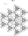
- FIG. 3 illustrates a plurality of unit cells 202 forming phased array antenna 102 in an illustrative example.
- FIG. 3 illustrates one possible configuration of phased array antenna 102, which is a non-rectangular array of unit cells 202.
- unit cells 202 When unit cells 202 are organized in an array as illustrated in FIG. 3 , unit cells 202 form a Tightly Coupled Dipole Array (TCDA).
- TCDA Tightly Coupled Dipole Array
- unit cell 202-1 and unit cell 202-2 are proximate to each other.
- Unit cell 202-1 includes a dipole antenna 302 and unit cell 202-2 includes a dipole antenna 303.
- Dipole antenna 302 is end-coupled to dipole antenna 303.
- antenna element 302-1 of dipole antenna 302 is electromagnetically coupled to antenna element 303-1 of dipole antenna 303. This process repeats for similar antenna element pairs.
- FIG. 4 illustrates a method 400 of fabricating a unit cell for a phased array antenna in an illustrative example.
- Method 400 will be described with respect to unit cell 202 illustrated in FIG. 2 , although method 400 may apply to other configurations for unit cell 202 in alternate examples.
- the steps of the methods described herein may include other steps, not shown. The steps may also be performed in a different order and/or combined in alternate examples.
- Step 402 of method 400 comprises obtaining a substrate having a first surface and a second surface that opposes the first surface (e.g., obtaining a dielectric substrate).
- the substrate may comprise a Printed Circuit Board (PCB) that includes a metal film on the first surface that is etched for form dipole antennas 204-206.
- the substrate may include other materials as desired.
- FIG. 5 illustrates a substrate 502 that includes a first surface 504 and a second surface 506 that opposes first surface 504 in an illustrative example.
- Step 404 of method 400 comprises forming a plurality of dipole antennas on first surface 504 that are arranged to collectively form a triangle.
- FIG. 6 illustrates substrate 502 that includes dipole antennas 204-206 formed on first surface 504 in an illustrative example.
- Fabricating dipole antennas 204-206 may comprise a deposition process, an etch process, etc., used to form or fabricate dipole antennas 204-206 onto first surface 504 of substrate 502. For instance, if substrate 502 comprises a PCB, then fabricating dipole antennas 204-206 may comprise etching a metal film applied to first surface 504 of substrate 502.
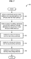
- FIG. 7 illustrates additional steps of method 400 in an illustrative example.
- steps 702-706 RF feedlines fabricated for unit cell 202 that electrically couple to dipole antennas 204-207.
- the RF feedlines may be used to provide electrical signals to dipole antennas 204-207, thereby causing them to operate in a transmit mode.
- the RF feedlines may also be used to receive electrical signals from dipole antennas 204-207, thereby causing them to operate in a receive mode.
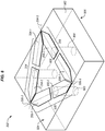
- FIG. 8 illustrates the result of performing steps 702-706 of method 400 in an illustrative example.
- an RF feedline 802 is electrically coupled to dipole antenna 204 (e.g., RF feedline 802 is electrically coupled to antenna element 204-2), an RF feedline 803 is electrically coupled to dipole antenna 205 (e.g., RF feedline 803 is electrically coupled to antenna element 205-2), and an RF feedline 804 is electrically coupled to dipole antenna 205 (e.g., RF feedline 804 is electrically coupled to antenna element 206-2).
- Fabricating RF feedlines 802-804 may be performed in a number of different ways. For example, RF feedlines 802-804 may fabricated using vias that traverse through substrate 502 between first surface 504 and second surface 506. However, other fabrication options exist for fabricating RF feedlines 802-804, including the use of RF striplines that electrically connect to each of dipole antennas 204-207.
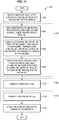
- FIG. 9 illustrates additional steps of method 400 in an illustrative example.
- steps 902-906 are directed to fabricating dipole antennas 204-206, which is illustrated in FIG. 6 .
- Step 908 of FIG. 9 describes forming electrical connections between a metal film on second surface 506 of substrate 502 and dipole antennas 204-206.
- Step 910 describes forming electrical connections to dipole antennas 204-206 (e.g., fabricating RF feedlines 802-804, previously described).
- FIG. 10 illustrates the result of performing steps 902-910 in an illustrative example.
- Substrate 502 includes a metal film 1002 on second surface 506.
- metal film 1002 may comprise one of the metal surface layers of the PCB that are etched during fabrication process for unit cell 202.
- FIG. 10 illustrates electrical connections 1004-1006 between dipole antennas 204-206 and metal film 1002.
- electrical connection 1004 electrically couples antenna element 204-1 of dipole antenna 204 to metal film 1002
- electrical connection 1005 electrically couples antenna element 205-1 to metal film 1002
- electrical connection 1006 electrically couples antenna element 206-1 to metal film 1002.
- Metal film 1002 may comprise a ground plane for dipole antennas 204-206 in some examples, while RF feedlines 802-804 are electrically isolated from metal film 1002.
- RF feedlines 802-804 may be electrically isolated from metal film 1002 using reliefs 1008-1010 on metal film 1002, respectively. Reliefs 1008-1010 may be formed by etching portions of metal film 1002 around locations on second surface 506 where RF feedlines 802-804 extend to second surface 506.
- FIG. 11 illustrates additional steps of method 400 in an illustrative example.
- substrate 502 comprises a PCB
- electrical connections 1004-1006 may be formed using vias (see step 1102 of FIG. 11 ), and RF feedlines 802-804 may also be formed using vias (see step 1104 of FIG. 11 ).
- Vias may be fabricated based on a drill and plating process, which includes mechanical or laser drilling through substrate 502, and plating the holes formed in substrate 502.
- a dielectric material may be formed on first surface 504 of substrate 502 (see step 1106 of FIG. 11 ).
- FIG. 12 illustrates a dielectric material 1202 applied to first surface 504 of substrate 502 in an illustrative example.
- Dielectric material 1202 may be used to provide physical protection to dipole antennas 204-206 and improve array scan performance.
- the dielectric constant and thickness of dielectric material 1202 may be determined using constrained optimization.
- a phase difference between RF feedlines 802-804 is generated.
- a relative phase offset between RF feedlines 802-804 may be one hundred and twenty degrees with respect to each other if dipole antennas 204-206 form an equilateral triangle.
- Either a clockwise or a counter-clockwise phase delay may be generated as desired.
- a clockwise phase delay results in a Left-Hand Circular Polarization (LHCP), while a counter-clockwise phase delay results in a Right-Hand Circular Polarization (RHCP).
- LHCP Left-Hand Circular Polarization
- RHCP Right-Hand Circular Polarization
- a LHCP may be formed, for example, when RF feedline 804 has a phase offset of zero degrees, RF feedline 803 has a phase offset of one hundred and twenty degrees, and RF feedline 802 has a phase offset of two hundred and forty degrees.
- a RHCP may be formed, for example, when RF feedline 804 has a phase offset of zero degrees, RF feedline 802 has a phase offset of one hundred and twenty degrees, and RF feedline 803 has a phase offset of two hundred and forty degrees.
- a perturbation from the one hundred and twenty degree phase delay increment is used to generate the optimum LHCP or RHCP.
- unit cell 202 may be fabricated onto a PCB and assembled into an array of unit cells 202 that form phased array antenna 102.
- the array of individual PCB tiles allows for the implementation of a wide variety of antenna apertures using unit cell.
- the proximity of the dipole antennas from one PCB tile to a neighboring PCB tile results in TCDA triangular lattice.
- phased array antenna 102 can be scaled to nearly any desired size using an array of unit cells 202 and can also be configured to have a particular shape or RF aperture using the triangular lattice formed from the configuration of dipole antennas 204-206 on unit cell 202.
- a PCB for unit cell 202 leverages existing PCB manufacturing processes and common PCB substrates, thereby allowing phased array antenna 102 to be fabricated from individual building blocks of unit cell 202.
- any of the various elements shown in the figures or described herein may be implemented as hardware, software, firmware, or some combination of these.
- an element may be implemented as dedicated hardware.
- Dedicated hardware elements may be referred to as "processors", “controllers”, or some similar terminology.
- processors When provided by a processor, the functions may be provided by a single dedicated processor, by a single shared processor, or by a plurality of individual processors, some of which may be shared.
- processor or “controller” should not be construed to refer exclusively to hardware capable of executing software, and may implicitly include, without limitation, digital signal processor (DSP) hardware, a network processor, application specific integrated circuit (ASIC) or other circuitry, field programmable gate array (FPGA), read only memory (ROM) for storing software, random access memory (RAM), non-volatile storage, logic, or some other physical hardware component or module.
- DSP digital signal processor
- ASIC application specific integrated circuit
- FPGA field programmable gate array
- ROM read only memory
- RAM random access memory
- non-volatile storage logic, or some other physical hardware component or module.
- an element may be implemented as instructions executable by a processor or a computer to perform the functions of the element.
- Some examples of instructions are software, program code, and firmware.
- the instructions are operational when executed by the processor to direct the processor to perform the functions of the element.
- the instructions may be stored on storage devices that are readable by the processor. Some examples of the storage devices are digital or solid-state memories, magnetic storage media such as a magnetic disks and magnetic tapes, hard drives, or optically readable digital data storage media.
- a phased array antenna comprising: at least one unit cell, comprising: a substrate having a first surface; and a plurality of dipole antennas arranged on the first surface to collectively form a triangle.
- the plurality of dipole antennas comprises a first dipole antenna, a second dipole antenna, and a third dipole antenna; and the at least one unit cell further comprises: a first a Radio Frequency (RF) feedline electrically coupled to the first dipole antenna; a second RF feedline electrically coupled to the second dipole antenna; and a third RF feedline electrically coupled to the third dipole antenna.
- RF Radio Frequency
- the phased array antenna of clause A1, wherein the plurality of dipole antennas comprises: a first dipole antenna having a first antenna element and second antenna element disposed along a first line; a second dipole antenna having a first antenna element and a second antenna element disposed along a second line, wherein the second line and the first line intersect at an angle of sixty degrees; and a third dipole antenna having a first antenna element and a second antenna element disposed along a third line, wherein the third line and each of the first line and the second line intersect at an angle of sixty degrees.
- the substrate further includes: a second surface opposing the first surface, wherein the second surface includes a metal film; first electrical connections between the metal film and the first antenna element of each of the first dipole antenna, the second dipole antenna, and the third dipole antenna; and second electrical connections to the second antenna element of each of the first dipole antenna, the second dipole antenna, and the third dipole antenna.
- RF Radio Frequency
- PCB Printed Circuit Board
- phased array antenna of clause A6 wherein the first electrical connections comprise: a first set of vias between the first surface of the PCB and the second surface of the PCB that electrically connect the first antenna element of each of the first dipole antenna, the second dipole antenna, and the third dipole antenna to the metal film on the second surface of the PCB.
- phased array antenna of clause A6 or A7 wherein the second electrical connections comprise: a second set of vias between the first surface of the PCB and the second surface of the PCB that are electrically connected to the second antenna element of each of the first dipole antenna, the second dipole antenna, and the third dipole antenna, and are electrically isolated from the metal film on the second surface of the PCB.
- TCDA Tightly Coupled Dipole Array
- a method of fabricating a unit cell for a phased array antenna comprising: obtaining a substrate having a first surface and a second surface that opposes the first surface; and forming a plurality of dipole antennas on the first surface that are arranged to collectively form a triangle.
- forming the plurality of dipole antennas further comprises: forming a first dipole antenna, a second dipole antenna, and a third dipole antenna on the first surface.
- forming the plurality of dipole antennas further comprises: forming a first dipole antenna having a first antenna element and second antenna element disposed along a first line; forming a second dipole antenna having a first antenna element and a second antenna element disposed along a second line, wherein the second line and the first line intersect at an angle of sixty degrees; and forming a third dipole antenna having a first antenna element and a second antenna element disposed along a third line, wherein the third line and each of the first line and the second line intersect at an angle of sixty degrees.
- the metal film comprises a ground plane for the first dipole antenna, the second dipole antenna, and the third dipole antenna; and the second electrical connections comprise Radio Frequency (RF) feed lines for the first dipole antenna, the second dipole antenna, and the third dipole antenna.
- RF Radio Frequency
- obtaining the substrate further comprises: obtaining a Printed Circuit Board (PCB).
- PCB Printed Circuit Board
- forming the first electrical connections comprises: fabricating a first set of vias between the first surface of the PCB and the second surface of the PCB that electrically connect the first antenna element of each of the first dipole antenna, the second dipole antenna, and the third dipole antenna to the metal film on the second surface of the PCB.
- phased array antenna of any of clauses A1 to A9 comprising: a plurality of unit cells, including the at least one unit cell, arranged to form a Tightly Coupled Dipole Array (TCDA) having a triangular lattice, each of the plurality of unit cells comprising: a substrate having a first surface; and a plurality of dipole antennas arranged on the first surface to collectively form a triangle.
- TCDA Tightly Coupled Dipole Array
- a phased array antenna comprising: a plurality of unit cells arranged to form a Tightly Coupled Dipole Array (TCDA) having a triangular lattice, each of the plurality of unit cells comprising: a substrate having a first surface; and a plurality of dipole antennas arranged on the first surface to collectively form a triangle.
- TCDA Tightly Coupled Dipole Array
- the phased array antenna of clause B1 or A19, wherein the plurality of dipole antennas comprises: a first dipole antenna having a first antenna element and second antenna element disposed along a first line; a second dipole antenna having a first antenna element and a second antenna element disposed along a second line, wherein the second line and the first line intersect at an angle of sixty degrees; and a third dipole antenna having a first antenna element and a second antenna element disposed along a third line, wherein the third line and each of the first line and the second line intersect at an angle of sixty degrees.
- the substrate further includes: a second surface opposing the first surface, wherein the second surface includes a metal film; first electrical connections between the metal film and the first antenna element of each of the first dipole antenna, the second dipole antenna, and the third dipole antenna; and second electrical connections to the second antenna element of each of the first dipole antenna, the second dipole antenna, and the third dipole antenna.
- phased array antenna of clause A21 wherein: the metal film comprises a ground plane for the first dipole antenna, the second dipole antenna, and the third dipole antenna; and the second electrical connections comprise Radio Frequency (RF) feedlines for the first dipole antenna, the second dipole antenna, and the third dipole antenna.
- RF Radio Frequency
- phased array antenna of clause A21 or A22 wherein: the substrate comprises a Printed Circuit Board (PCB).
- PCB Printed Circuit Board
- phased array antenna of claim A23 wherein the first electrical connections comprise: a first set of vias between the first surface of the PCB and the second surface of the PCB that electrically connect the first antenna element of each of the first dipole antenna, the second dipole antenna, and the third dipole antenna to the metal film on the second surface of the PCB.
- phased array antenna of claim A23 or A24 wherein the second electrical connections comprise: a second set of vias between the first surface of the PCB and the second surface of the PCB that are electrically connected to the second antenna element of each of the first dipole antenna, the second dipole antenna, and the third dipole antenna, and are electrically isolated from the metal film on the second surface of the PCB.
Landscapes
- Engineering & Computer Science (AREA)
- Remote Sensing (AREA)
- Physics & Mathematics (AREA)
- General Physics & Mathematics (AREA)
- Astronomy & Astrophysics (AREA)
- Aviation & Aerospace Engineering (AREA)
- Radar, Positioning & Navigation (AREA)
- Computer Networks & Wireless Communication (AREA)
- Manufacturing & Machinery (AREA)
- Variable-Direction Aerials And Aerial Arrays (AREA)
Abstract
Description
- This disclosure relates to the field of phased arrays, and in particular, to phased array antennas that are formed from an array of unit cell antennas.
- Phased arrays are electromagnetic antenna systems that include a large number of antenna elements along with electronics connected to the antenna elements that perform beam forming. The antenna elements are typically positioned in an orderly grid within the antenna aperture.
- When the phased array is in a receive mode, each of the antenna elements capture some portion of the Radio Frequency (RF) energy from incoming signals and convert the RF energy into separate electrical signals that are fed to the electronics. The electronics utilize reconfigurable gain and phase delays for the separate electrical signals in order to generate a spatial filter that strongly favors signals arriving from a specific direction. This favored direction represents the look angle of its beam, with the shape of the beam adjustable based on weighting factors applied to the separate electrical signals.
- When the phased array is in a transmit mode, electrical signals generated by the electronics are fed to the antenna elements, which convert the electrical signals into radiant energy. The control electronics vary the phase relationship between the antenna elements such that radio waves from the separate antenna elements add together to increase radiation in a desired direction, while cancelling to suppress radiation in undesired directions.
- One current solution utilizes relatively bulky and narrow-band waveguides having a circular cross-section to form the aperture of the phased array antenna. However, this and other existing solutions cannot meet ultra-wide bandwidth while scanning and other requirements for some applications that are currently being developed.
- It is therefore evident that phased array antennas may be improved in order to support ultra-wideband applications that are in use today.
- Unit cells for phased array antennas are described. The unit cells include a plurality of dipole antennas that are used to form an array for a phased array antenna. In particular, the unit cells that form the phased array antenna each include a plurality of dipole antennas formed on a surface of a substrate that are arranged to collectively form a triangle. A plurality of the unit cells may be linked together to form a triangular lattice array having almost any desired size and antenna aperture, thereby allowing the RF engineer the freedom to achieve a wide variety of performance goals when designing a phased array antenna.
- One example comprises a phased array antenna that includes at least one unit cell. The at least one unit cell includes a substrate having a first surface and a plurality of dipole antennas arranged on the first surface to collectively form a triangle.
- Another example comprises a method of fabricating a unit cell for a phased array antenna. The method comprises obtaining a substrate having a first surface and a second surface that opposes the first surface. The method further comprises forming a plurality of dipole antennas on the first surface that are arranged to collectively form a triangle.
- Another example comprises a phased array antenna. The phased array antenna includes a plurality of unit cells arranged to form a Tightly Coupled Dipole Array (TCDA) having a triangular lattice. Each of the unit cells comprise a substrate having a first surface, and a plurality of dipole antennas arranged on the first surface to collectively form a triangle.
- The features, functions, and advantages that have been discussed can be achieved independently in various examples or may be combined in yet other examples, further details of which can be seen with reference to the following description and drawings.
- Some examples are now described with reference to the accompanying drawings. The same reference number represents the same element or the same type of element on all drawings.
-
FIG. 1 illustrates an airborne mobile platform having a phased array antenna in an illustrative example. -
FIG. 2 illustrates a unit cell for a phased array antenna in an illustrative example. -
FIG. 3 illustrates a plurality of unit cells forming a phased array antenna in an illustrative example. -
FIG. 4 illustrates a method of fabricating a unit cell for a phased array antenna in an illustrative example. -
FIGS. 5-6 illustrate the result of performing steps of the method ofFIG.4 in an illustrative example. -
FIG. 7 illustrates additional steps of the method ofFIG. 4 in an illustrative example. -
FIG. 8 illustrates the result of performing the additional steps described inFIG. 7 in an illustrative example. -
FIG. 9 illustrates additional steps of the method ofFIG. 4 in an illustrative example. -
FIG. 10 illustrates the result of performing the additional steps described inFIG. 9 in an illustrative example. -
FIG. 11 illustrates additional steps of the method ofFIG. 4 in an illustrative example. -
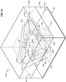
FIG. 12 illustrates the result of performing the additional steps described inFIG. 11 in an illustrative example. - The figures and the following description illustrate specific examples. It will be appreciated that those skilled in the art will be able to devise various arrangements that, although not explicitly described or shown herein, embody the principles described herein and are included within the contemplated scope of the claims that follow this description. Furthermore, any examples described herein are intended to aid in understanding the principles of the disclosure are to be construed as being without limitation. As a result, this disclosure is not limited to the specific examples described below, but by the claims.
- Phased arrays have gained acceptance over traditional mechanical scanning antennas because they allow for rapid beam steering electronically, rather than mechanically. The term "phased array" and "Electronically Scanned Array" (ESA) are often used interchangeably. Older generation phased arrays were implemented as a Passive Electronically Scanned Array (PESA). In PESAs, the antenna elements in the phased array are connected to a single transmitter and/or receiver through adjustable phase shifters.
- Modern advances in electronics have led to the development of Active Electronically Scanned Arrays (AESAs) that utilize solid state transmit/receive modules (TRMs) that are communicatively coupled to each antenna element of the phased array. Compared to PESAs that use phase shifters connected to a single source, the use of TRMs allow for the control of phase, gain, and frequency at an individual radiating element in the phased array. AESAs are considered a more sophisticated version of a PESA. While a PESA can only emit a single beam of radio waves at a single frequency at a time, AESAs can radiate multiple beams of radio waves at multiple frequencies simultaneously. Most modern aircraft implement Radio Detection and Ranging (RADAR) system using AESA.
- While RADAR is one use of phased arrays, other uses may include wireless communication and Electronic Warfare (EW). Phased arrays are useful in providing bi-directional communication capabilities to mobile platforms due to the ability to perform beamforming without mechanically moving the antenna. For example, an aircraft in flight may utilize a phased array antenna to communicate with one or more satellites by electronically steering the phased array antenna to track a satellite rather than mechanically moving an antenna. While the aircraft is in flight, the pitch, yaw, and roll of the aircraft can be compensated for electronically using electronic steering of the phased array rather than mechanical steering of a traditional antenna. This improves the reliability of the data connection. In EW applications, the phased array can operate as a jammer using beamforming directed at a target. Ultra-wideband provides additional capabilities in engaging frequency-diverse targets. In receive-only mode such as Signal Intelligence (SigInt), ultra-wideband covers signals of interest over a wider frequency spectrum.
- Phased arrays have increasingly been implemented using PCB fabrication techniques to provide flexibility in the design of the phased array and the integration of Radio Frequency (RF) circuits. In some cases, unit cells for the phased array are formed from PCBs that include antenna elements. These unit cells may be combined as desired to form an array of PCBs, thereby allowing for flexibility in the geometry of the phased array. However, existing unit cells for phased arrays in ultra-wideband (UWB) applications utilize a rectangular lattice, which lacks flexibility in implementing various geometries of phased arrays. Phased arrays that utilize UWB capable cells are desired, as they enable the phased array antenna to operate over a wider frequency band. For instance, UWB phased arrays may be useful in high-bandwidth communications, UWB RADAR implementation, and UWB EW implementations.
- In the examples described herein, unit cells are described that utilize a triangular dipole configuration that when combined to form a phased array antenna, implement a triangular lattice. The use of a triangular lattice in UWB phased arrays allows for about a fifteen percent larger unit cell size over rectangular arrays without compromising the grating-lobe free maximum can limit. Further, the triangular lattice phased array antenna is more suitable for electronics integration at millimeter wavelengths due to the larger unit cell size. Further, the use of a triangular lattice phased array antenna also provides more flexibility to form non-rectangular antenna apertures, which may be used to improve RF performance, including the ability to achieve sidelobe level targets, the ability to reduce cross-polarization, and the ability to improve other parameters over scan volume and/or observation field-of-view. Other solutions such as connected arrays or Tightly Coupled Arrays (TCA) can meet ultra-wide bandwidth while scanning but in general rely on a rectangular or square array lattice rather than the more desirable triangular lattice. The present disclosure combines ultra-wide bandwidth while scanning and a triangular lattice. The advantages of a triangular lattice include larger allowable unit cell size and thus reduced RF packaging, improved cross-polarization or axial ratio performance at scan.
-
FIG. 1 illustrates amobile platform 100 having a phasedarray antenna 102 in an illustrative example. In this example,mobile platform 100 is an aircraft having a particular configuration, although in other examplesmobile platform 100 may include other aircraft, both manned and unmanned, having different configurations as desired.Mobile platform 100 may include drones, missiles, vehicles, stationary communication installations, hand-held communication equipment, etc., as desired. Thus, the particular illustration with respect tomobile platform 100 inFIG. 1 is merely for purposes of discussion. - In this example,
mobile platform 100 communicates with one or more satellite(s) 104 using phasedarray antenna 102, although in other examples phasedarray antenna 102 may be used to communicate with other entities that utilize Common Data Link (CDL) protocols. In this example, phasedarray antenna 102 provides a bi-directional communication link betweenmobile platform 100 and satellite(s) 104. For example, phasedarray antenna 102 may communicate with satellite(s) 104 to provide high speed bi-directional data services tomobile platform 100 over the Ka-band, which covers frequencies from 26.5 GHz to 40 GHz. One example of a Ka-band data service that may be provided by satellite(s) 104 includes the Inmarsat Global Xpress (GX) program. In other examples, phasedarray antenna 102 may be utilized to implement RADAR (e.g., UWB RADAR) or EW (e.g., UWB EW). In the examples described herein, phasedarray antenna 102 is formed from a plurality of unit cells, which form an elemental antenna unit for phasedarray antenna 102. In particular, the unit cells include a plurality of dipole antennas arranged on a surface of a substrate to form an equilateral triangle. Generally, the unit cells described herein are RF building blocks for phased array antennas. For instance, if the unit cells are implemented on a PCB, then individual PCBs forming the unit cells may be arranged in an array to form a phased array antenna. -
FIG. 2 illustrates aunit cell 202 for a phased array antenna (e.g., phased array antenna 102) in an illustrative example. In this example,unit cell 202 includes dipole antennas 204-206 formed onto asubstrate 502, which collectively form a triangle.Dipole antenna 204 includes antenna element 204-1 and antenna element 204-2, which are disposed along a line 204-3 and are separated by a gap 204-4. Antenna element 204-1 includes a portion 204-5 proximate to gap 204-4, and a portion 204-6 distal from gap 204-4. Portion 204-6 is proximate to aperimeter 201 ofsubstrate 502 and is tapered. Antenna element 204-2 includes a portion 204-7 proximate to gap 204-4, and a portion 204-8 distal from gap 204-4. Portion 204-8 is proximate toperimeter 201 of substrate and is tapered. -
Dipole antenna 205 includes antenna element 205-1 and antenna element 205-2, which are disposed along a line 205-3 and are separated by a gap 205-4. Antenna element 205-1 includes a portion 205-5 proximate to gap 205-4, and a portion 205-6 distal from gap 205-4. Portion 205-6 is proximate toperimeter 201 ofsubstrate 502 and is tapered. Antenna element 205-2 includes a portion 205-7 proximate to gap 205-4, and a portion 205-8 distal from gap 205-4. Portion 205-8 is proximate toperimeter 201 of substrate and is tapered. Line 204-3 and line 205-3 intersect at an angle 205-9 of sixty degrees. Portion 204-8 and portion 205-6 are separated by a gap 205-10. -
Dipole antenna 206 includes antenna element 206-1 and antenna element 206-2, which are disposed along a line 206-3 and are separated by a gap 206-4. Antenna element 206-1 includes a portion 206-5 proximate to gap 206-4, and a portion 206-6 distal from gap 206-4. Portion 206-6 is proximate toperimeter 201 ofsubstrate 502 and is tapered. Antenna element 206-2 includes a portion 206-7 proximate to gap 206-4, and a portion 206-8 distal from gap 206-4. Portion 206-8 is proximate toperimeter 201 of substrate and is tapered. Line 206-3 and line 205-3 intersect at an angle 206-9 of sixty degrees. Portion 205-8 and portion 206-6 are separated by a gap 206-10. Line 206-3 and line 204-3 intersect at an angle 204-9 of sixty degrees. In addition, portion 204-6 and portion 206-8 are separated by gap 204-10. -
FIG. 3 illustrates a plurality ofunit cells 202 forming phasedarray antenna 102 in an illustrative example.FIG. 3 illustrates one possible configuration of phasedarray antenna 102, which is a non-rectangular array ofunit cells 202. However, due to the flexibility of combiningunit cell 202 into a plurality of different array configurations for phasedarray antenna 102, one of ordinary skill in the art will recognize that different array configurations may be implemented as desired. Whenunit cells 202 are organized in an array as illustrated inFIG. 3 ,unit cells 202 form a Tightly Coupled Dipole Array (TCDA). For example, unit cell 202-1 and unit cell 202-2 are proximate to each other. Unit cell 202-1 includes adipole antenna 302 and unit cell 202-2 includes adipole antenna 303.Dipole antenna 302 is end-coupled todipole antenna 303. In particular, antenna element 302-1 ofdipole antenna 302 is electromagnetically coupled to antenna element 303-1 ofdipole antenna 303. This process repeats for similar antenna element pairs. -
FIG. 4 illustrates amethod 400 of fabricating a unit cell for a phased array antenna in an illustrative example.Method 400 will be described with respect tounit cell 202 illustrated inFIG. 2 , althoughmethod 400 may apply to other configurations forunit cell 202 in alternate examples. The steps of the methods described herein may include other steps, not shown. The steps may also be performed in a different order and/or combined in alternate examples. - Step 402 of
method 400 comprises obtaining a substrate having a first surface and a second surface that opposes the first surface (e.g., obtaining a dielectric substrate). For example, the substrate may comprise a Printed Circuit Board (PCB) that includes a metal film on the first surface that is etched for form dipole antennas 204-206. However, the substrate may include other materials as desired.FIG. 5 illustrates asubstrate 502 that includes afirst surface 504 and asecond surface 506 that opposesfirst surface 504 in an illustrative example. Step 404 ofmethod 400 comprises forming a plurality of dipole antennas onfirst surface 504 that are arranged to collectively form a triangle.FIG. 6 illustratessubstrate 502 that includes dipole antennas 204-206 formed onfirst surface 504 in an illustrative example. Fabricating dipole antennas 204-206 may comprise a deposition process, an etch process, etc., used to form or fabricate dipole antennas 204-206 ontofirst surface 504 ofsubstrate 502. For instance, ifsubstrate 502 comprises a PCB, then fabricating dipole antennas 204-206 may comprise etching a metal film applied tofirst surface 504 ofsubstrate 502. -
FIG. 7 illustrates additional steps ofmethod 400 in an illustrative example. In steps 702-706, RF feedlines fabricated forunit cell 202 that electrically couple to dipole antennas 204-207. The RF feedlines may be used to provide electrical signals to dipole antennas 204-207, thereby causing them to operate in a transmit mode. The RF feedlines may also be used to receive electrical signals from dipole antennas 204-207, thereby causing them to operate in a receive mode.FIG. 8 illustrates the result of performing steps 702-706 ofmethod 400 in an illustrative example. In particular, anRF feedline 802 is electrically coupled to dipole antenna 204 (e.g.,RF feedline 802 is electrically coupled to antenna element 204-2), anRF feedline 803 is electrically coupled to dipole antenna 205 (e.g.,RF feedline 803 is electrically coupled to antenna element 205-2), and anRF feedline 804 is electrically coupled to dipole antenna 205 (e.g.,RF feedline 804 is electrically coupled to antenna element 206-2). Fabricating RF feedlines 802-804 may be performed in a number of different ways. For example, RF feedlines 802-804 may fabricated using vias that traverse throughsubstrate 502 betweenfirst surface 504 andsecond surface 506. However, other fabrication options exist for fabricating RF feedlines 802-804, including the use of RF striplines that electrically connect to each of dipole antennas 204-207. -
FIG. 9 illustrates additional steps ofmethod 400 in an illustrative example. In particular, steps 902-906 are directed to fabricating dipole antennas 204-206, which is illustrated inFIG. 6 . Step 908 ofFIG. 9 describes forming electrical connections between a metal film onsecond surface 506 ofsubstrate 502 and dipole antennas 204-206. Step 910 describes forming electrical connections to dipole antennas 204-206 (e.g., fabricating RF feedlines 802-804, previously described).FIG. 10 illustrates the result of performing steps 902-910 in an illustrative example.Substrate 502 includes ametal film 1002 onsecond surface 506. For instance, ifsubstrate 502 is a PCB, thenmetal film 1002 may comprise one of the metal surface layers of the PCB that are etched during fabrication process forunit cell 202.FIG. 10 illustrates electrical connections 1004-1006 between dipole antennas 204-206 andmetal film 1002. In particular,electrical connection 1004 electrically couples antenna element 204-1 ofdipole antenna 204 tometal film 1002,electrical connection 1005 electrically couples antenna element 205-1 tometal film 1002, andelectrical connection 1006 electrically couples antenna element 206-1 tometal film 1002.Metal film 1002 may comprise a ground plane for dipole antennas 204-206 in some examples, while RF feedlines 802-804 are electrically isolated frommetal film 1002. RF feedlines 802-804 may be electrically isolated frommetal film 1002 using reliefs 1008-1010 onmetal film 1002, respectively. Reliefs 1008-1010 may be formed by etching portions ofmetal film 1002 around locations onsecond surface 506 where RF feedlines 802-804 extend tosecond surface 506. -
FIG. 11 illustrates additional steps ofmethod 400 in an illustrative example. In particular, whensubstrate 502 comprises a PCB, then electrical connections 1004-1006 may be formed using vias (seestep 1102 ofFIG. 11 ), and RF feedlines 802-804 may also be formed using vias (seestep 1104 ofFIG. 11 ). Vias may be fabricated based on a drill and plating process, which includes mechanical or laser drilling throughsubstrate 502, and plating the holes formed insubstrate 502. - In some examples, a dielectric material may be formed on
first surface 504 of substrate 502 (seestep 1106 ofFIG. 11 ).FIG. 12 illustrates adielectric material 1202 applied tofirst surface 504 ofsubstrate 502 in an illustrative example.Dielectric material 1202 may be used to provide physical protection to dipole antennas 204-206 and improve array scan performance. The dielectric constant and thickness ofdielectric material 1202 may be determined using constrained optimization. - To create a circular polarization for
unit cell 202 illustrated inFIG. 12 , a phase difference between RF feedlines 802-804 is generated. For example, a relative phase offset between RF feedlines 802-804 may be one hundred and twenty degrees with respect to each other if dipole antennas 204-206 form an equilateral triangle. Either a clockwise or a counter-clockwise phase delay may be generated as desired. For example, a clockwise phase delay results in a Left-Hand Circular Polarization (LHCP), while a counter-clockwise phase delay results in a Right-Hand Circular Polarization (RHCP). If dipole antennas 204-206 form an equilateral triangle, then a LHCP may be formed, for example, when RF feedline 804 has a phase offset of zero degrees,RF feedline 803 has a phase offset of one hundred and twenty degrees, andRF feedline 802 has a phase offset of two hundred and forty degrees. A RHCP may be formed, for example, when RF feedline 804 has a phase offset of zero degrees,RF feedline 802 has a phase offset of one hundred and twenty degrees, andRF feedline 803 has a phase offset of two hundred and forty degrees. For a non-equilateral triangular lattice, a perturbation from the one hundred and twenty degree phase delay increment is used to generate the optimum LHCP or RHCP. - As discussed previously,
unit cell 202 may be fabricated onto a PCB and assembled into an array ofunit cells 202 that form phasedarray antenna 102. The array of individual PCB tiles allows for the implementation of a wide variety of antenna apertures using unit cell. As discussed with respect toFIG. 3 , the proximity of the dipole antennas from one PCB tile to a neighboring PCB tile results in TCDA triangular lattice. - Utilizing
unit cell 202, phasedarray antenna 102 can be scaled to nearly any desired size using an array ofunit cells 202 and can also be configured to have a particular shape or RF aperture using the triangular lattice formed from the configuration of dipole antennas 204-206 onunit cell 202. A PCB forunit cell 202 leverages existing PCB manufacturing processes and common PCB substrates, thereby allowing phasedarray antenna 102 to be fabricated from individual building blocks ofunit cell 202. - Any of the various elements shown in the figures or described herein may be implemented as hardware, software, firmware, or some combination of these. For example, an element may be implemented as dedicated hardware. Dedicated hardware elements may be referred to as "processors", "controllers", or some similar terminology. When provided by a processor, the functions may be provided by a single dedicated processor, by a single shared processor, or by a plurality of individual processors, some of which may be shared. Moreover, explicit use of the term "processor" or "controller" should not be construed to refer exclusively to hardware capable of executing software, and may implicitly include, without limitation, digital signal processor (DSP) hardware, a network processor, application specific integrated circuit (ASIC) or other circuitry, field programmable gate array (FPGA), read only memory (ROM) for storing software, random access memory (RAM), non-volatile storage, logic, or some other physical hardware component or module.
- Also, an element may be implemented as instructions executable by a processor or a computer to perform the functions of the element. Some examples of instructions are software, program code, and firmware. The instructions are operational when executed by the processor to direct the processor to perform the functions of the element. The instructions may be stored on storage devices that are readable by the processor. Some examples of the storage devices are digital or solid-state memories, magnetic storage media such as a magnetic disks and magnetic tapes, hard drives, or optically readable digital data storage media.
- Further examples are set forth in the following clauses.
- A1. A phased array antenna, comprising: at least one unit cell, comprising: a substrate having a first surface; and a plurality of dipole antennas arranged on the first surface to collectively form a triangle.
- A2. The phased array antenna of clause A1, wherein: the plurality of dipole antennas comprises a first dipole antenna, a second dipole antenna, and a third dipole antenna; and
the at least one unit cell further comprises: a first a Radio Frequency (RF) feedline electrically coupled to the first dipole antenna; a second RF feedline electrically coupled to the second dipole antenna; and a third RF feedline electrically coupled to the third dipole antenna. - A3. The phased array antenna of clause A1, wherein the plurality of dipole antennas comprises: a first dipole antenna having a first antenna element and second antenna element disposed along a first line; a second dipole antenna having a first antenna element and a second antenna element disposed along a second line, wherein the second line and the first line intersect at an angle of sixty degrees; and a third dipole antenna having a first antenna element and a second antenna element disposed along a third line, wherein the third line and each of the first line and the second line intersect at an angle of sixty degrees.
- A4. The phased array antenna of clause A3, wherein the substrate further includes: a second surface opposing the first surface, wherein the second surface includes a metal film; first electrical connections between the metal film and the first antenna element of each of the first dipole antenna, the second dipole antenna, and the third dipole antenna; and second electrical connections to the second antenna element of each of the first dipole antenna, the second dipole antenna, and the third dipole antenna.
- A5. The phased array antenna of clause A4, wherein: the metal film comprises a ground plane for the first dipole antenna, the second dipole antenna, and the third dipole antenna; and the second electrical connections comprise Radio Frequency (RF) feed lines for the first dipole antenna, the second dipole antenna, and the third dipole antenna.
- A6. The phased array antenna of clause A4 or A5, wherein: the substrate comprises a Printed Circuit Board (PCB).
- A7. The phased array antenna of clause A6, wherein the first electrical connections comprise: a first set of vias between the first surface of the PCB and the second surface of the PCB that electrically connect the first antenna element of each of the first dipole antenna, the second dipole antenna, and the third dipole antenna to the metal film on the second surface of the PCB.
- A8. The phased array antenna of clause A6 or A7, wherein the second electrical connections comprise: a second set of vias between the first surface of the PCB and the second surface of the PCB that are electrically connected to the second antenna element of each of the first dipole antenna, the second dipole antenna, and the third dipole antenna, and are electrically isolated from the metal film on the second surface of the PCB.
- A9. The phased array antenna of any of clauses A1 to A8, further comprising: a plurality of the at least one unit cell arranged in an array to form a Tightly Coupled Dipole Array (TCDA) having a triangular lattice.
- A10. A method of fabricating a unit cell for a phased array antenna, the method comprising: obtaining a substrate having a first surface and a second surface that opposes the first surface; and forming a plurality of dipole antennas on the first surface that are arranged to collectively form a triangle.
- A11. The method of clause A10, wherein forming the plurality of dipole antennas further comprises: forming a first dipole antenna, a second dipole antenna, and a third dipole antenna on the first surface.
- A12. The method of clause A11, further comprising:fabricating a first Radio Frequency (RF) feedline that electrically couples to the first dipole antenna; fabricating a second RF feedline that electrically couples to the second dipole antenna; and fabricating a third RF feedline that electrically couples to the third dipole antenna.
- A13. The method of any of clauses A10 to A12, wherein forming the plurality of dipole antennas further comprises: forming a first dipole antenna having a first antenna element and second antenna element disposed along a first line; forming a second dipole antenna having a first antenna element and a second antenna element disposed along a second line, wherein the second line and the first line intersect at an angle of sixty degrees; and forming a third dipole antenna having a first antenna element and a second antenna element disposed along a third line, wherein the third line and each of the first line and the second line intersect at an angle of sixty degrees.
- A14. The method of clause A13, further comprising: forming first electrical connections between a metal film on the second surface and the first antenna element of each of the first dipole antenna, the second dipole antenna, and the third dipole antenna; and forming second electrical connections to the second antenna element of each of the first dipole antenna, the second dipole antenna, and the third dipole antenna.
- A15. The method of clause A14, wherein: the metal film comprises a ground plane for the first dipole antenna, the second dipole antenna, and the third dipole antenna; and the second electrical connections comprise Radio Frequency (RF) feed lines for the first dipole antenna, the second dipole antenna, and the third dipole antenna.
- A16. The method of clause A14 or A15, wherein obtaining the substrate further comprises: obtaining a Printed Circuit Board (PCB).
- A17. The method of clause A16, wherein forming the first electrical connections comprises: fabricating a first set of vias between the first surface of the PCB and the second surface of the PCB that electrically connect the first antenna element of each of the first dipole antenna, the second dipole antenna, and the third dipole antenna to the metal film on the second surface of the PCB.
- A18. The method of clause A16 or A17, wherein forming the second electrical connections comprises fabricating a second set of vias between the first surface of the PCB and the second surface of the PCB that are electrically connected to the second antenna element of each of the first dipole antenna, the second dipole antenna, and the third dipole antenna, and are electrically isolated from the metal film on the second surface of the PCB.
- B1. The phased array antenna of any of clauses A1 to A9, comprising:a plurality of unit cells, including the at least one unit cell, arranged to form a Tightly Coupled Dipole Array (TCDA) having a triangular lattice, each of the plurality of unit cells comprising: a substrate having a first surface; and a plurality of dipole antennas arranged on the first surface to collectively form a triangle.
- A19. A phased array antenna, comprising: a plurality of unit cells arranged to form a Tightly Coupled Dipole Array (TCDA) having a triangular lattice, each of the plurality of unit cells comprising: a substrate having a first surface; and a plurality of dipole antennas arranged on the first surface to collectively form a triangle.
- A20. The phased array antenna of clause B1 or A19, wherein the plurality of dipole antennas comprises: a first dipole antenna having a first antenna element and second antenna element disposed along a first line; a second dipole antenna having a first antenna element and a second antenna element disposed along a second line, wherein the second line and the first line intersect at an angle of sixty degrees; and a third dipole antenna having a first antenna element and a second antenna element disposed along a third line, wherein the third line and each of the first line and the second line intersect at an angle of sixty degrees.
- A21. The phased array antenna of clause A20, wherein the substrate further includes: a second surface opposing the first surface, wherein the second surface includes a metal film; first electrical connections between the metal film and the first antenna element of each of the first dipole antenna, the second dipole antenna, and the third dipole antenna; and second electrical connections to the second antenna element of each of the first dipole antenna, the second dipole antenna, and the third dipole antenna.
- A22. The phased array antenna of clause A21, wherein: the metal film comprises a ground plane for the first dipole antenna, the second dipole antenna, and the third dipole antenna; and the second electrical connections comprise Radio Frequency (RF) feedlines for the first dipole antenna, the second dipole antenna, and the third dipole antenna.
- A23. The phased array antenna of clause A21 or A22, wherein: the substrate comprises a Printed Circuit Board (PCB).
- A24. The phased array antenna of claim A23, wherein the first electrical connections comprise: a first set of vias between the first surface of the PCB and the second surface of the PCB that electrically connect the first antenna element of each of the first dipole antenna, the second dipole antenna, and the third dipole antenna to the metal film on the second surface of the PCB.
- A25. The phased array antenna of claim A23 or A24, wherein the second electrical connections comprise: a second set of vias between the first surface of the PCB and the second surface of the PCB that are electrically connected to the second antenna element of each of the first dipole antenna, the second dipole antenna, and the third dipole antenna, and are electrically isolated from the metal film on the second surface of the PCB.
- Although specific examples were described herein, the scope is not limited to those specific examples. Rather, the scope is defined by the following claims.
Claims (15)
- A phased array antenna, comprising:at least one unit cell, comprising:
a substrate having a first surface; anda plurality of dipole antennas arranged on the first surface to collectively form a triangle. - The phased array antenna of claim 1, wherein:the plurality of dipole antennas comprises a first dipole antenna, a second dipole antenna, and a third dipole antenna; andthe at least one unit cell further comprises:a first a Radio Frequency (RF) feedline electrically coupled to the first dipole antenna;a second RF feedline electrically coupled to the second dipole antenna; anda third RF feedline electrically coupled to the third dipole antenna.
- The phased array antenna of claim 1, wherein the plurality of dipole antennas comprises:a first dipole antenna having a first antenna element and second antenna element disposed along a first line;a second dipole antenna having a first antenna element and a second antenna element disposed along a second line, wherein the second line and the first line intersect at an angle of sixty degrees; anda third dipole antenna having a first antenna element and a second antenna element disposed along a third line, wherein the third line and each of the first line and the second line intersect at an angle of sixty degrees.
- The phased array antenna of claim 3, wherein the substrate further includes:a second surface opposing the first surface, wherein the second surface includes a metal film;first electrical connections between the metal film and the first antenna element of each of the first dipole antenna, the second dipole antenna, and the third dipole antenna; andsecond electrical connections to the second antenna element of each of the first dipole antenna, the second dipole antenna, and the third dipole antenna.
- The phased array antenna of claim 4, wherein:the metal film comprises a ground plane for the first dipole antenna, the second dipole antenna, and the third dipole antenna; andthe second electrical connections comprise Radio Frequency (RF) feed lines for the first dipole antenna, the second dipole antenna, and the third dipole antenna.
- The phased array antenna of claim 4 or 5, wherein:
the substrate comprises a Printed Circuit Board (PCB); and, optionally:wherein the first electrical connections comprise a first set of vias between the first surface of the PCB and the second surface of the PCB that electrically connect the first antenna element of each of the first dipole antenna, the second dipole antenna, and the third dipole antenna to the metal film on the second surface of the PCB; and/orwherein the second electrical connections comprise a second set of vias between the first surface of the PCB and the second surface of the PCB that are electrically connected to the second antenna element of each of the first dipole antenna, the second dipole antenna, and the third dipole antenna, and are electrically isolated from the metal film on the second surface of the PCB. - The phased array antenna of any preceding claim, further comprising:
a plurality of the at least one unit cell arranged in an array to form a Tightly Coupled Dipole Array (TCDA) having a triangular lattice. - The phased array antenna of any preceding claim, comprising:
a plurality of unit cells, including the at least one unit cell, arranged to form a Tightly Coupled Dipole Array (TCDA) having a triangular lattice, each of the plurality of unit cells comprising:a substrate having a first surface; anda plurality of dipole antennas arranged on the first surface to collectively form a triangle. - An aircraft comprising the phased array antenna of any preceding claim.
- A method of fabricating a unit cell for a phased array antenna, the method comprising:obtaining a substrate having a first surface and a second surface that opposes the first surface; andforming a plurality of dipole antennas on the first surface that are arranged to collectively form a triangle.
- The method of claim 10, wherein forming the plurality of dipole antennas further comprises:
forming a first dipole antenna, a second dipole antenna, and a third dipole antenna on the first surface. - The method of claim 10 or 11, wherein forming the plurality of dipole antennas further comprises:forming a first dipole antenna having a first antenna element and second antenna element disposed along a first line;forming a second dipole antenna having a first antenna element and a second antenna element disposed along a second line, wherein the second line and the first line intersect at an angle of sixty degrees; andforming a third dipole antenna having a first antenna element and a second antenna element disposed along a third line, wherein the third line and each of the first line and the second line intersect at an angle of sixty degrees.
- The method of claim 12, further comprising:forming first electrical connections between a metal film on the second surface and the first antenna element of each of the first dipole antenna, the second dipole antenna, and the third dipole antenna; andforming second electrical connections to the second antenna element of each of the first dipole antenna, the second dipole antenna, and the third dipole antenna.
- The method of claim 13, wherein:the metal film comprises a ground plane for the first dipole antenna, the second dipole antenna, and the third dipole antenna; andthe second electrical connections comprise Radio Frequency (RF) feed lines for the first dipole antenna, the second dipole antenna, and the third dipole antenna.
- The method of claim 13 or 14, wherein obtaining the substrate further comprises:
obtaining a Printed Circuit Board (PCB); and, optionally:wherein forming the first electrical connections comprises fabricating a first set of vias between the first surface of the PCB and the second surface of the PCB that electrically connect the first antenna element of each of the first dipole antenna, the second dipole antenna, and the third dipole antenna to the metal film on the second surface of the PCB; and/orwherein forming the second electrical connections comprises fabricating a second set of vias between the first surface of the PCB and the second surface of the PCB that are electrically connected to the second antenna element of each of the first dipole antenna, the second dipole antenna, and the third dipole antenna, and are electrically isolated from the metal film on the second surface of the PCB.
Applications Claiming Priority (1)
| Application Number | Priority Date | Filing Date | Title |
|---|---|---|---|
| US15/959,995 US10651566B2 (en) | 2018-04-23 | 2018-04-23 | Unit cell antenna for phased arrays |
Publications (2)
| Publication Number | Publication Date |
|---|---|
| EP3561951A1 true EP3561951A1 (en) | 2019-10-30 |
| EP3561951B1 EP3561951B1 (en) | 2022-10-12 |
Family
ID=66248584
Family Applications (1)
| Application Number | Title | Priority Date | Filing Date |
|---|---|---|---|
| EP19170534.2A Active EP3561951B1 (en) | 2018-04-23 | 2019-04-23 | Unit cell antenna for phased arrays |
Country Status (5)
| Country | Link |
|---|---|
| US (1) | US10651566B2 (en) |
| EP (1) | EP3561951B1 (en) |
| JP (1) | JP7366580B2 (en) |
| KR (1) | KR102623004B1 (en) |
| CN (1) | CN110391495B (en) |
Cited By (1)
| Publication number | Priority date | Publication date | Assignee | Title |
|---|---|---|---|---|
| WO2021198990A1 (en) * | 2020-04-03 | 2021-10-07 | Isotropic Systems Ltd | Field-assembled modular phased array satcom terminal |
Families Citing this family (14)
| Publication number | Priority date | Publication date | Assignee | Title |
|---|---|---|---|---|
| CN113543863B (en) | 2019-02-28 | 2025-09-23 | 奇跃公司 | Method and system for six-degree-of-freedom tracking of a transmitter in an augmented reality system using phased array beamforming |
| EP3959774A1 (en) | 2019-04-26 | 2022-03-02 | Battelle Memorial Institute | Systems and methods for signal communication with scalable, modular network nodes |
| US11936415B2 (en) | 2019-05-03 | 2024-03-19 | Battelle Memorial Institute | Modular radio frequency aperture |
| USD1113875S1 (en) | 2020-04-24 | 2026-02-17 | Battelle Memorial Institute | Interface board for radio frequency antenna |
| CN112162036B (en) * | 2020-09-16 | 2022-01-11 | 昆明理工大学 | Health monitoring system and method for regular triangle phased array bolt fastening structure |
| US11539146B2 (en) * | 2021-03-19 | 2022-12-27 | United States Of America As Represented By The Secretary Of The Navy | Circular polarized phased array with wideband axial ratio bandwidth using sequential rotation and dynamic phase recovery |
| US12160039B2 (en) | 2022-02-14 | 2024-12-03 | The Boeing Company | Unit cell antenna for phased arrays |
| US12034216B2 (en) * | 2022-02-19 | 2024-07-09 | Motorola Mobility Llc | Pivoting millimeter-wave antenna assembly and corresponding electronic devices and methods |
| US11909120B1 (en) * | 2022-09-26 | 2024-02-20 | Lockheed Martin Corporation | Magnetoelectric antenna array |
| US12537298B2 (en) * | 2023-02-02 | 2026-01-27 | Panasonic Avionics Corporation | Thermal load balancing for electronically steerable antennas |
| WO2024226042A1 (en) * | 2023-04-26 | 2024-10-31 | Battelle Memorial Institute | Air interface plane for radio frequency aperture |
| US11901930B1 (en) | 2023-04-26 | 2024-02-13 | Battelle Memorial Institute | Radio frequency aperture with cooling assembly |
| US11967767B1 (en) | 2023-04-26 | 2024-04-23 | Battelle Memorial Institute | Air interface plane for radio frequency aperture |
| WO2025253660A1 (en) * | 2024-06-06 | 2025-12-11 | 三菱電機株式会社 | Circularly polarized antenna device |
Citations (3)
| Publication number | Priority date | Publication date | Assignee | Title |
|---|---|---|---|---|
| US6512487B1 (en) * | 2000-10-31 | 2003-01-28 | Harris Corporation | Wideband phased array antenna and associated methods |
| US20080191955A1 (en) * | 2005-04-29 | 2008-08-14 | Telefonaktiebolaget Lm Ericsson (Publ) | A Triple Polarized Clover Antenna With Dipoles |
| US7965252B2 (en) * | 2004-08-18 | 2011-06-21 | Ruckus Wireless, Inc. | Dual polarization antenna array with increased wireless coverage |
Family Cites Families (27)
| Publication number | Priority date | Publication date | Assignee | Title |
|---|---|---|---|---|
| US4126866A (en) * | 1977-05-17 | 1978-11-21 | Ohio State University Research Foundation | Space filter surface |
| DE69809704T2 (en) * | 1998-02-12 | 2003-04-10 | Sony International (Europe) Gmbh | Antenna support structure |
| FI114586B (en) * | 1999-11-01 | 2004-11-15 | Filtronic Lk Oy | flat Antenna |
| US7196674B2 (en) * | 2003-11-21 | 2007-03-27 | Andrew Corporation | Dual polarized three-sector base station antenna with variable beam tilt |
| US7498996B2 (en) * | 2004-08-18 | 2009-03-03 | Ruckus Wireless, Inc. | Antennas with polarization diversity |
| US20060044189A1 (en) * | 2004-09-01 | 2006-03-02 | Livingston Stan W | Radome structure |
| US7463210B2 (en) * | 2007-04-05 | 2008-12-09 | Harris Corporation | Phased array antenna formed as coupled dipole array segments |
| WO2010033865A2 (en) * | 2008-09-19 | 2010-03-25 | Rayspan Corporation | Metamaterial loaded antenna devices |
| WO2011064587A1 (en) * | 2009-11-27 | 2011-06-03 | Bae Systems Plc | Radar antenna |
| KR101053442B1 (en) * | 2009-12-04 | 2011-08-02 | 주식회사 에이스테크놀로지 | Dual polarized dipole antenna with improved feed structure |
| US9735473B2 (en) * | 2010-09-17 | 2017-08-15 | Blackberry Limited | Compact radiation structure for diversity antennas |
| US8743015B1 (en) * | 2010-09-29 | 2014-06-03 | Rockwell Collins, Inc. | Omni-directional ultra wide band miniature doubly curved antenna array |
| ITTO20110301A1 (en) * | 2011-04-01 | 2012-10-02 | Telecom Italia Spa | DOUBLE-POLARIZED ANTENNA AND SWITCHED-BAND ANTENNA FOR RADIO-COMMUNICATION DEVICES |
| US9368879B1 (en) * | 2011-05-25 | 2016-06-14 | The Boeing Company | Ultra wide band antenna element |
| US9099777B1 (en) * | 2011-05-25 | 2015-08-04 | The Boeing Company | Ultra wide band antenna element |
| EP2717385B1 (en) * | 2011-06-02 | 2020-05-06 | Panasonic Corporation | Antenna apparatus |
| US9190734B2 (en) * | 2011-08-09 | 2015-11-17 | New Jersey Institute Of Technology | Broadband circularly polarized bent-dipole based antennas |
| KR20130098098A (en) * | 2012-02-27 | 2013-09-04 | 한국전자통신연구원 | High-gain wideband antenna apparatus |
| KR20130112518A (en) * | 2012-04-04 | 2013-10-14 | 엘에스전선 주식회사 | Dual polarization dipole antenna for broad-band and antenna array using it |
| US10224637B2 (en) * | 2012-07-09 | 2019-03-05 | Jasmin ROY | Reciprocal circular polarization selective surfaces and elements thereof |
| JP2014143591A (en) * | 2013-01-24 | 2014-08-07 | Nippon Dengyo Kosaku Co Ltd | Array antenna |
| GB201314242D0 (en) * | 2013-08-08 | 2013-09-25 | Univ Manchester | Wide band array antenna |
| US9488893B2 (en) * | 2014-09-02 | 2016-11-08 | The Boeing Company | Active finish system for providing an image on a surface |
| US9735475B2 (en) * | 2014-12-01 | 2017-08-15 | Anderson Contract Engineering, Inc. | Low cost antenna array and methods of manufacture |
| US9653810B2 (en) * | 2015-06-12 | 2017-05-16 | City University Of Hong Kong | Waveguide fed and wideband complementary antenna |
| CA2992289A1 (en) * | 2015-07-22 | 2017-01-26 | Blue Danube Systems, Inc. | A modular phased array |
| WO2017038045A1 (en) * | 2015-08-31 | 2017-03-09 | パナソニックIpマネジメント株式会社 | Antenna device |
-
2018
- 2018-04-23 US US15/959,995 patent/US10651566B2/en active Active
-
2019
- 2019-04-22 JP JP2019080951A patent/JP7366580B2/en active Active
- 2019-04-22 KR KR1020190046856A patent/KR102623004B1/en active Active
- 2019-04-23 EP EP19170534.2A patent/EP3561951B1/en active Active
- 2019-04-23 CN CN201910327513.6A patent/CN110391495B/en active Active
Patent Citations (3)
| Publication number | Priority date | Publication date | Assignee | Title |
|---|---|---|---|---|
| US6512487B1 (en) * | 2000-10-31 | 2003-01-28 | Harris Corporation | Wideband phased array antenna and associated methods |
| US7965252B2 (en) * | 2004-08-18 | 2011-06-21 | Ruckus Wireless, Inc. | Dual polarization antenna array with increased wireless coverage |
| US20080191955A1 (en) * | 2005-04-29 | 2008-08-14 | Telefonaktiebolaget Lm Ericsson (Publ) | A Triple Polarized Clover Antenna With Dipoles |
Non-Patent Citations (1)
| Title |
|---|
| ANTONIO-DANIELE CAPOBIANCO ET AL: "A Compact MIMO Array of Planar End-Fire Antennas for WLAN Applications", IEEE TRANSACTIONS ON ANTENNAS AND PROPAGATION, IEEE SERVICE CENTER, PISCATAWAY, NJ, US, vol. 59, no. 9, 1 September 2011 (2011-09-01), pages 3462 - 3465, XP011359253, ISSN: 0018-926X, DOI: 10.1109/TAP.2011.2161557 * |
Cited By (3)
| Publication number | Priority date | Publication date | Assignee | Title |
|---|---|---|---|---|
| WO2021198990A1 (en) * | 2020-04-03 | 2021-10-07 | Isotropic Systems Ltd | Field-assembled modular phased array satcom terminal |
| US11581639B2 (en) | 2020-04-03 | 2023-02-14 | All.Space Networks Ltd. | Field-assembled modular phased array SATCOM terminal |
| US11996626B2 (en) | 2020-04-03 | 2024-05-28 | All.Space Networks Limited | Field-assembled modular phased array SATCOM terminal |
Also Published As
| Publication number | Publication date |
|---|---|
| CN110391495B (en) | 2023-06-16 |
| KR20190123236A (en) | 2019-10-31 |
| US20190326685A1 (en) | 2019-10-24 |
| EP3561951B1 (en) | 2022-10-12 |
| KR102623004B1 (en) | 2024-01-08 |
| JP2019193264A (en) | 2019-10-31 |
| JP7366580B2 (en) | 2023-10-27 |
| US10651566B2 (en) | 2020-05-12 |
| CN110391495A (en) | 2019-10-29 |
Similar Documents
| Publication | Publication Date | Title |
|---|---|---|
| EP3561951B1 (en) | Unit cell antenna for phased arrays | |
| Chaloun et al. | Design of a dual-polarized stacked patch antenna for wide-angle scanning reflectarrays | |
| US10283876B1 (en) | Dual-polarized, planar slot-aperture antenna element | |
| EP2551959B1 (en) | Wide-band linked-ring antenna element for phased arrays | |
| US20190074588A1 (en) | Lens antenna system | |
| US20210159597A1 (en) | High-gain, wide-angle, multi-beam, multi-frequency beamforming lens antenna | |
| US10910712B2 (en) | Active electronically scanned array (AESA) antenna configuration for simultaneous transmission and receiving of communication signals | |
| US10978812B2 (en) | Single layer shared aperture dual band antenna | |
| Gao et al. | Antennas for small satellites | |
| EP3410533A1 (en) | Wideband antenna system | |
| US20250210860A1 (en) | Low cost electronically scanning antenna array architecture | |
| US10236572B2 (en) | Radio frequency chokes for integrated phased-array antennas | |
| AU2021273812A1 (en) | A high-gain, hemi-spherical coverage, multi-sided flattened luneburg lens antenna | |
| US8604997B1 (en) | Vertical array antenna | |
| Reis et al. | General Overview of Antennas for Unmanned Aerial Vehicles: A Review | |
| US12021305B1 (en) | Conformal antenna system | |
| US11223126B1 (en) | Combined cross-link and communication-link phased array for satellite communication | |
| Milias et al. | Metasurface-based, pattern-reconfigurable, wide-angle scanning antenna array for UAV-borne radar | |
| Sanad et al. | A multibeam antenna for multi-orbit LEO satellites and terminals with a very simple tracking technique | |
| Baggen et al. | Phased array technology by IMST: A comprehensive overview | |
| Son et al. | Phased array antenna for bi-static simultaneous transmit and receive (STAR) system | |
| Jeong et al. | Printed dipole antenna array with reconfigurable feeding network for wide elevation angle of U2X communications | |
| Kedar et al. | Parametric Analysis of Unmanned Aerial Vehicle Based Antenna Arrays | |
| Engroff et al. | Comparison of beamforming algorithms for retro-directive arrays with faulty elements | |
| Liao et al. | Omnidirectional Multibeam Substrate Integrated Horn Array for Unmanned Aerial Vehicles |
Legal Events
| Date | Code | Title | Description |
|---|---|---|---|
| PUAI | Public reference made under article 153(3) epc to a published international application that has entered the european phase |
Free format text: ORIGINAL CODE: 0009012 |
|
| STAA | Information on the status of an ep patent application or granted ep patent |
Free format text: STATUS: REQUEST FOR EXAMINATION WAS MADE |
|
| 17P | Request for examination filed |
Effective date: 20190423 |
|
| AK | Designated contracting states |
Kind code of ref document: A1 Designated state(s): AL AT BE BG CH CY CZ DE DK EE ES FI FR GB GR HR HU IE IS IT LI LT LU LV MC MK MT NL NO PL PT RO RS SE SI SK SM TR |
|
| AX | Request for extension of the european patent |
Extension state: BA ME |
|
| STAA | Information on the status of an ep patent application or granted ep patent |
Free format text: STATUS: EXAMINATION IS IN PROGRESS |
|
| 17Q | First examination report despatched |
Effective date: 20210209 |
|
| GRAP | Despatch of communication of intention to grant a patent |
Free format text: ORIGINAL CODE: EPIDOSNIGR1 |
|
| STAA | Information on the status of an ep patent application or granted ep patent |
Free format text: STATUS: GRANT OF PATENT IS INTENDED |
|
| INTG | Intention to grant announced |
Effective date: 20211102 |
|
| GRAJ | Information related to disapproval of communication of intention to grant by the applicant or resumption of examination proceedings by the epo deleted |
Free format text: ORIGINAL CODE: EPIDOSDIGR1 |
|
| STAA | Information on the status of an ep patent application or granted ep patent |
Free format text: STATUS: EXAMINATION IS IN PROGRESS |
|
| INTC | Intention to grant announced (deleted) | ||
| GRAP | Despatch of communication of intention to grant a patent |
Free format text: ORIGINAL CODE: EPIDOSNIGR1 |
|
| STAA | Information on the status of an ep patent application or granted ep patent |
Free format text: STATUS: GRANT OF PATENT IS INTENDED |
|
| INTG | Intention to grant announced |
Effective date: 20220426 |
|
| GRAS | Grant fee paid |
Free format text: ORIGINAL CODE: EPIDOSNIGR3 |
|
| GRAA | (expected) grant |
Free format text: ORIGINAL CODE: 0009210 |
|
| STAA | Information on the status of an ep patent application or granted ep patent |
Free format text: STATUS: THE PATENT HAS BEEN GRANTED |
|
| AK | Designated contracting states |
Kind code of ref document: B1 Designated state(s): AL AT BE BG CH CY CZ DE DK EE ES FI FR GB GR HR HU IE IS IT LI LT LU LV MC MK MT NL NO PL PT RO RS SE SI SK SM TR |
|
| REG | Reference to a national code |
Ref country code: GB Ref legal event code: FG4D |
|
| REG | Reference to a national code |
Ref country code: CH Ref legal event code: EP |
|
| REG | Reference to a national code |
Ref country code: DE Ref legal event code: R096 Ref document number: 602019020442 Country of ref document: DE |
|
| REG | Reference to a national code |
Ref country code: IE Ref legal event code: FG4D |
|
| REG | Reference to a national code |
Ref country code: AT Ref legal event code: REF Ref document number: 1524724 Country of ref document: AT Kind code of ref document: T Effective date: 20221115 |
|
| REG | Reference to a national code |
Ref country code: LT Ref legal event code: MG9D |
|
| REG | Reference to a national code |
Ref country code: NL Ref legal event code: MP Effective date: 20221012 |
|
| REG | Reference to a national code |
Ref country code: AT Ref legal event code: MK05 Ref document number: 1524724 Country of ref document: AT Kind code of ref document: T Effective date: 20221012 |
|
| RAP4 | Party data changed (patent owner data changed or rights of a patent transferred) |
Owner name: THE BOEING COMPANY |
|
| PG25 | Lapsed in a contracting state [announced via postgrant information from national office to epo] |
Ref country code: NL Free format text: LAPSE BECAUSE OF FAILURE TO SUBMIT A TRANSLATION OF THE DESCRIPTION OR TO PAY THE FEE WITHIN THE PRESCRIBED TIME-LIMIT Effective date: 20221012 |
|
| PG25 | Lapsed in a contracting state [announced via postgrant information from national office to epo] |
Ref country code: SE Free format text: LAPSE BECAUSE OF FAILURE TO SUBMIT A TRANSLATION OF THE DESCRIPTION OR TO PAY THE FEE WITHIN THE PRESCRIBED TIME-LIMIT Effective date: 20221012 Ref country code: PT Free format text: LAPSE BECAUSE OF FAILURE TO SUBMIT A TRANSLATION OF THE DESCRIPTION OR TO PAY THE FEE WITHIN THE PRESCRIBED TIME-LIMIT Effective date: 20230213 Ref country code: NO Free format text: LAPSE BECAUSE OF FAILURE TO SUBMIT A TRANSLATION OF THE DESCRIPTION OR TO PAY THE FEE WITHIN THE PRESCRIBED TIME-LIMIT Effective date: 20230112 Ref country code: LT Free format text: LAPSE BECAUSE OF FAILURE TO SUBMIT A TRANSLATION OF THE DESCRIPTION OR TO PAY THE FEE WITHIN THE PRESCRIBED TIME-LIMIT Effective date: 20221012 Ref country code: FI Free format text: LAPSE BECAUSE OF FAILURE TO SUBMIT A TRANSLATION OF THE DESCRIPTION OR TO PAY THE FEE WITHIN THE PRESCRIBED TIME-LIMIT Effective date: 20221012 Ref country code: ES Free format text: LAPSE BECAUSE OF FAILURE TO SUBMIT A TRANSLATION OF THE DESCRIPTION OR TO PAY THE FEE WITHIN THE PRESCRIBED TIME-LIMIT Effective date: 20221012 Ref country code: AT Free format text: LAPSE BECAUSE OF FAILURE TO SUBMIT A TRANSLATION OF THE DESCRIPTION OR TO PAY THE FEE WITHIN THE PRESCRIBED TIME-LIMIT Effective date: 20221012 |
|
| PG25 | Lapsed in a contracting state [announced via postgrant information from national office to epo] |
Ref country code: RS Free format text: LAPSE BECAUSE OF FAILURE TO SUBMIT A TRANSLATION OF THE DESCRIPTION OR TO PAY THE FEE WITHIN THE PRESCRIBED TIME-LIMIT Effective date: 20221012 Ref country code: PL Free format text: LAPSE BECAUSE OF FAILURE TO SUBMIT A TRANSLATION OF THE DESCRIPTION OR TO PAY THE FEE WITHIN THE PRESCRIBED TIME-LIMIT Effective date: 20221012 Ref country code: LV Free format text: LAPSE BECAUSE OF FAILURE TO SUBMIT A TRANSLATION OF THE DESCRIPTION OR TO PAY THE FEE WITHIN THE PRESCRIBED TIME-LIMIT Effective date: 20221012 Ref country code: IS Free format text: LAPSE BECAUSE OF FAILURE TO SUBMIT A TRANSLATION OF THE DESCRIPTION OR TO PAY THE FEE WITHIN THE PRESCRIBED TIME-LIMIT Effective date: 20230212 Ref country code: HR Free format text: LAPSE BECAUSE OF FAILURE TO SUBMIT A TRANSLATION OF THE DESCRIPTION OR TO PAY THE FEE WITHIN THE PRESCRIBED TIME-LIMIT Effective date: 20221012 Ref country code: GR Free format text: LAPSE BECAUSE OF FAILURE TO SUBMIT A TRANSLATION OF THE DESCRIPTION OR TO PAY THE FEE WITHIN THE PRESCRIBED TIME-LIMIT Effective date: 20230113 |
|
| P01 | Opt-out of the competence of the unified patent court (upc) registered |
Effective date: 20230516 |
|
| REG | Reference to a national code |
Ref country code: DE Ref legal event code: R097 Ref document number: 602019020442 Country of ref document: DE |
|
| PG25 | Lapsed in a contracting state [announced via postgrant information from national office to epo] |
Ref country code: SM Free format text: LAPSE BECAUSE OF FAILURE TO SUBMIT A TRANSLATION OF THE DESCRIPTION OR TO PAY THE FEE WITHIN THE PRESCRIBED TIME-LIMIT Effective date: 20221012 Ref country code: RO Free format text: LAPSE BECAUSE OF FAILURE TO SUBMIT A TRANSLATION OF THE DESCRIPTION OR TO PAY THE FEE WITHIN THE PRESCRIBED TIME-LIMIT Effective date: 20221012 Ref country code: EE Free format text: LAPSE BECAUSE OF FAILURE TO SUBMIT A TRANSLATION OF THE DESCRIPTION OR TO PAY THE FEE WITHIN THE PRESCRIBED TIME-LIMIT Effective date: 20221012 Ref country code: DK Free format text: LAPSE BECAUSE OF FAILURE TO SUBMIT A TRANSLATION OF THE DESCRIPTION OR TO PAY THE FEE WITHIN THE PRESCRIBED TIME-LIMIT Effective date: 20221012 Ref country code: CZ Free format text: LAPSE BECAUSE OF FAILURE TO SUBMIT A TRANSLATION OF THE DESCRIPTION OR TO PAY THE FEE WITHIN THE PRESCRIBED TIME-LIMIT Effective date: 20221012 |
|
| PLBE | No opposition filed within time limit |
Free format text: ORIGINAL CODE: 0009261 |
|
| STAA | Information on the status of an ep patent application or granted ep patent |
Free format text: STATUS: NO OPPOSITION FILED WITHIN TIME LIMIT |
|
| PG25 | Lapsed in a contracting state [announced via postgrant information from national office to epo] |
Ref country code: SK Free format text: LAPSE BECAUSE OF FAILURE TO SUBMIT A TRANSLATION OF THE DESCRIPTION OR TO PAY THE FEE WITHIN THE PRESCRIBED TIME-LIMIT Effective date: 20221012 Ref country code: AL Free format text: LAPSE BECAUSE OF FAILURE TO SUBMIT A TRANSLATION OF THE DESCRIPTION OR TO PAY THE FEE WITHIN THE PRESCRIBED TIME-LIMIT Effective date: 20221012 |
|
| 26N | No opposition filed |
Effective date: 20230713 |
|
| PG25 | Lapsed in a contracting state [announced via postgrant information from national office to epo] |
Ref country code: SI Free format text: LAPSE BECAUSE OF FAILURE TO SUBMIT A TRANSLATION OF THE DESCRIPTION OR TO PAY THE FEE WITHIN THE PRESCRIBED TIME-LIMIT Effective date: 20221012 |
|
| REG | Reference to a national code |
Ref country code: CH Ref legal event code: PL |
|
| PG25 | Lapsed in a contracting state [announced via postgrant information from national office to epo] |
Ref country code: LU Free format text: LAPSE BECAUSE OF NON-PAYMENT OF DUE FEES Effective date: 20230423 |
|
| REG | Reference to a national code |
Ref country code: BE Ref legal event code: MM Effective date: 20230430 |
|
| PG25 | Lapsed in a contracting state [announced via postgrant information from national office to epo] |
Ref country code: MC Free format text: LAPSE BECAUSE OF FAILURE TO SUBMIT A TRANSLATION OF THE DESCRIPTION OR TO PAY THE FEE WITHIN THE PRESCRIBED TIME-LIMIT Effective date: 20221012 |
|
| PG25 | Lapsed in a contracting state [announced via postgrant information from national office to epo] |
Ref country code: MC Free format text: LAPSE BECAUSE OF FAILURE TO SUBMIT A TRANSLATION OF THE DESCRIPTION OR TO PAY THE FEE WITHIN THE PRESCRIBED TIME-LIMIT Effective date: 20221012 Ref country code: LI Free format text: LAPSE BECAUSE OF NON-PAYMENT OF DUE FEES Effective date: 20230430 Ref country code: CH Free format text: LAPSE BECAUSE OF NON-PAYMENT OF DUE FEES Effective date: 20230430 |
|
| REG | Reference to a national code |
Ref country code: IE Ref legal event code: MM4A |
|
| PG25 | Lapsed in a contracting state [announced via postgrant information from national office to epo] |
Ref country code: BE Free format text: LAPSE BECAUSE OF NON-PAYMENT OF DUE FEES Effective date: 20230430 |
|
| PG25 | Lapsed in a contracting state [announced via postgrant information from national office to epo] |
Ref country code: IE Free format text: LAPSE BECAUSE OF NON-PAYMENT OF DUE FEES Effective date: 20230423 |
|
| PG25 | Lapsed in a contracting state [announced via postgrant information from national office to epo] |
Ref country code: IE Free format text: LAPSE BECAUSE OF NON-PAYMENT OF DUE FEES Effective date: 20230423 |
|
| PG25 | Lapsed in a contracting state [announced via postgrant information from national office to epo] |
Ref country code: IT Free format text: LAPSE BECAUSE OF FAILURE TO SUBMIT A TRANSLATION OF THE DESCRIPTION OR TO PAY THE FEE WITHIN THE PRESCRIBED TIME-LIMIT Effective date: 20221012 |
|
| PG25 | Lapsed in a contracting state [announced via postgrant information from national office to epo] |
Ref country code: BG Free format text: LAPSE BECAUSE OF FAILURE TO SUBMIT A TRANSLATION OF THE DESCRIPTION OR TO PAY THE FEE WITHIN THE PRESCRIBED TIME-LIMIT Effective date: 20221012 |
|
| PG25 | Lapsed in a contracting state [announced via postgrant information from national office to epo] |
Ref country code: BG Free format text: LAPSE BECAUSE OF FAILURE TO SUBMIT A TRANSLATION OF THE DESCRIPTION OR TO PAY THE FEE WITHIN THE PRESCRIBED TIME-LIMIT Effective date: 20221012 |
|
| PGFP | Annual fee paid to national office [announced via postgrant information from national office to epo] |
Ref country code: DE Payment date: 20250429 Year of fee payment: 7 |
|
| PGFP | Annual fee paid to national office [announced via postgrant information from national office to epo] |
Ref country code: GB Payment date: 20250428 Year of fee payment: 7 |
|
| PGFP | Annual fee paid to national office [announced via postgrant information from national office to epo] |
Ref country code: FR Payment date: 20250425 Year of fee payment: 7 |
|
| PG25 | Lapsed in a contracting state [announced via postgrant information from national office to epo] |
Ref country code: CY Free format text: LAPSE BECAUSE OF FAILURE TO SUBMIT A TRANSLATION OF THE DESCRIPTION OR TO PAY THE FEE WITHIN THE PRESCRIBED TIME-LIMIT; INVALID AB INITIO Effective date: 20190423 |
|
| PG25 | Lapsed in a contracting state [announced via postgrant information from national office to epo] |
Ref country code: HU Free format text: LAPSE BECAUSE OF FAILURE TO SUBMIT A TRANSLATION OF THE DESCRIPTION OR TO PAY THE FEE WITHIN THE PRESCRIBED TIME-LIMIT; INVALID AB INITIO Effective date: 20190423 |
|
| PG25 | Lapsed in a contracting state [announced via postgrant information from national office to epo] |
Ref country code: TR Free format text: LAPSE BECAUSE OF FAILURE TO SUBMIT A TRANSLATION OF THE DESCRIPTION OR TO PAY THE FEE WITHIN THE PRESCRIBED TIME-LIMIT Effective date: 20221012 |