EP3561867A1 - A power semiconductor device with a double island surface mount package - Google Patents
A power semiconductor device with a double island surface mount package Download PDFInfo
- Publication number
- EP3561867A1 EP3561867A1 EP19165579.4A EP19165579A EP3561867A1 EP 3561867 A1 EP3561867 A1 EP 3561867A1 EP 19165579 A EP19165579 A EP 19165579A EP 3561867 A1 EP3561867 A1 EP 3561867A1
- Authority
- EP
- European Patent Office
- Prior art keywords
- metal layer
- dice
- package
- regions
- die
- Prior art date
- Legal status (The legal status is an assumption and is not a legal conclusion. Google has not performed a legal analysis and makes no representation as to the accuracy of the status listed.)
- Granted
Links
Images



Classifications
-
- H—ELECTRICITY
- H10—SEMICONDUCTOR DEVICES; ELECTRIC SOLID-STATE DEVICES NOT OTHERWISE PROVIDED FOR
- H10W—GENERIC PACKAGES, INTERCONNECTIONS, CONNECTORS OR OTHER CONSTRUCTIONAL DETAILS OF DEVICES COVERED BY CLASS H10
- H10W70/00—Package substrates; Interposers; Redistribution layers [RDL]
- H10W70/60—Insulating or insulated package substrates; Interposers; Redistribution layers
- H10W70/62—Insulating or insulated package substrates; Interposers; Redistribution layers characterised by their interconnections
- H10W70/65—Shapes or dispositions of interconnections
- H10W70/658—Shapes or dispositions of interconnections for devices provided for in groups H10D8/00 - H10D48/00
-
- H—ELECTRICITY
- H10—SEMICONDUCTOR DEVICES; ELECTRIC SOLID-STATE DEVICES NOT OTHERWISE PROVIDED FOR
- H10W—GENERIC PACKAGES, INTERCONNECTIONS, CONNECTORS OR OTHER CONSTRUCTIONAL DETAILS OF DEVICES COVERED BY CLASS H10
- H10W74/00—Encapsulations, e.g. protective coatings
- H10W74/10—Encapsulations, e.g. protective coatings characterised by their shape or disposition
- H10W74/131—Encapsulations, e.g. protective coatings characterised by their shape or disposition the semiconductor body being only partially enclosed
- H10W74/137—Encapsulations, e.g. protective coatings characterised by their shape or disposition the semiconductor body being only partially enclosed the encapsulations being directly on the semiconductor body
-
- H—ELECTRICITY
- H10—SEMICONDUCTOR DEVICES; ELECTRIC SOLID-STATE DEVICES NOT OTHERWISE PROVIDED FOR
- H10W—GENERIC PACKAGES, INTERCONNECTIONS, CONNECTORS OR OTHER CONSTRUCTIONAL DETAILS OF DEVICES COVERED BY CLASS H10
- H10W74/00—Encapsulations, e.g. protective coatings
- H10W74/10—Encapsulations, e.g. protective coatings characterised by their shape or disposition
- H10W74/111—Encapsulations, e.g. protective coatings characterised by their shape or disposition the semiconductor body being completely enclosed
-
- H—ELECTRICITY
- H10—SEMICONDUCTOR DEVICES; ELECTRIC SOLID-STATE DEVICES NOT OTHERWISE PROVIDED FOR
- H10W—GENERIC PACKAGES, INTERCONNECTIONS, CONNECTORS OR OTHER CONSTRUCTIONAL DETAILS OF DEVICES COVERED BY CLASS H10
- H10W40/00—Arrangements for thermal protection or thermal control
- H10W40/20—Arrangements for cooling
- H10W40/25—Arrangements for cooling characterised by their materials
- H10W40/255—Arrangements for cooling characterised by their materials having a laminate or multilayered structure, e.g. direct bond copper [DBC] ceramic substrates
-
- H—ELECTRICITY
- H10—SEMICONDUCTOR DEVICES; ELECTRIC SOLID-STATE DEVICES NOT OTHERWISE PROVIDED FOR
- H10W—GENERIC PACKAGES, INTERCONNECTIONS, CONNECTORS OR OTHER CONSTRUCTIONAL DETAILS OF DEVICES COVERED BY CLASS H10
- H10W40/00—Arrangements for thermal protection or thermal control
- H10W40/70—Fillings or auxiliary members in containers or in encapsulations for thermal protection or control
- H10W40/77—Auxiliary members characterised by their shape
- H10W40/778—Auxiliary members characterised by their shape in encapsulations
-
- H—ELECTRICITY
- H10—SEMICONDUCTOR DEVICES; ELECTRIC SOLID-STATE DEVICES NOT OTHERWISE PROVIDED FOR
- H10W—GENERIC PACKAGES, INTERCONNECTIONS, CONNECTORS OR OTHER CONSTRUCTIONAL DETAILS OF DEVICES COVERED BY CLASS H10
- H10W70/00—Package substrates; Interposers; Redistribution layers [RDL]
- H10W70/40—Leadframes
- H10W70/421—Shapes or dispositions
- H10W70/424—Cross-sectional shapes
-
- H—ELECTRICITY
- H10—SEMICONDUCTOR DEVICES; ELECTRIC SOLID-STATE DEVICES NOT OTHERWISE PROVIDED FOR
- H10W—GENERIC PACKAGES, INTERCONNECTIONS, CONNECTORS OR OTHER CONSTRUCTIONAL DETAILS OF DEVICES COVERED BY CLASS H10
- H10W70/00—Package substrates; Interposers; Redistribution layers [RDL]
- H10W70/40—Leadframes
- H10W70/461—Leadframes specially adapted for cooling
-
- H—ELECTRICITY
- H10—SEMICONDUCTOR DEVICES; ELECTRIC SOLID-STATE DEVICES NOT OTHERWISE PROVIDED FOR
- H10W—GENERIC PACKAGES, INTERCONNECTIONS, CONNECTORS OR OTHER CONSTRUCTIONAL DETAILS OF DEVICES COVERED BY CLASS H10
- H10W70/00—Package substrates; Interposers; Redistribution layers [RDL]
- H10W70/40—Leadframes
- H10W70/464—Additional interconnections in combination with leadframes
- H10W70/467—Multilayered additional interconnections
-
- H—ELECTRICITY
- H10—SEMICONDUCTOR DEVICES; ELECTRIC SOLID-STATE DEVICES NOT OTHERWISE PROVIDED FOR
- H10W—GENERIC PACKAGES, INTERCONNECTIONS, CONNECTORS OR OTHER CONSTRUCTIONAL DETAILS OF DEVICES COVERED BY CLASS H10
- H10W70/00—Package substrates; Interposers; Redistribution layers [RDL]
- H10W70/60—Insulating or insulated package substrates; Interposers; Redistribution layers
- H10W70/67—Insulating or insulated package substrates; Interposers; Redistribution layers characterised by their insulating layers or insulating parts
- H10W70/68—Shapes or dispositions thereof
- H10W70/685—Shapes or dispositions thereof comprising multiple insulating layers
-
- H—ELECTRICITY
- H10—SEMICONDUCTOR DEVICES; ELECTRIC SOLID-STATE DEVICES NOT OTHERWISE PROVIDED FOR
- H10W—GENERIC PACKAGES, INTERCONNECTIONS, CONNECTORS OR OTHER CONSTRUCTIONAL DETAILS OF DEVICES COVERED BY CLASS H10
- H10W90/00—Package configurations
-
- H—ELECTRICITY
- H10—SEMICONDUCTOR DEVICES; ELECTRIC SOLID-STATE DEVICES NOT OTHERWISE PROVIDED FOR
- H10W—GENERIC PACKAGES, INTERCONNECTIONS, CONNECTORS OR OTHER CONSTRUCTIONAL DETAILS OF DEVICES COVERED BY CLASS H10
- H10W90/00—Package configurations
- H10W90/811—Multiple chips on leadframes
-
- H—ELECTRICITY
- H10—SEMICONDUCTOR DEVICES; ELECTRIC SOLID-STATE DEVICES NOT OTHERWISE PROVIDED FOR
- H10W—GENERIC PACKAGES, INTERCONNECTIONS, CONNECTORS OR OTHER CONSTRUCTIONAL DETAILS OF DEVICES COVERED BY CLASS H10
- H10W72/00—Interconnections or connectors in packages
- H10W72/071—Connecting or disconnecting
- H10W72/073—Connecting or disconnecting of die-attach connectors
- H10W72/07331—Connecting techniques
- H10W72/07336—Soldering or alloying
-
- H—ELECTRICITY
- H10—SEMICONDUCTOR DEVICES; ELECTRIC SOLID-STATE DEVICES NOT OTHERWISE PROVIDED FOR
- H10W—GENERIC PACKAGES, INTERCONNECTIONS, CONNECTORS OR OTHER CONSTRUCTIONAL DETAILS OF DEVICES COVERED BY CLASS H10
- H10W72/00—Interconnections or connectors in packages
- H10W72/071—Connecting or disconnecting
- H10W72/073—Connecting or disconnecting of die-attach connectors
- H10W72/07351—Connecting or disconnecting of die-attach connectors characterised by changes in properties of the die-attach connectors during connecting
- H10W72/07354—Connecting or disconnecting of die-attach connectors characterised by changes in properties of the die-attach connectors during connecting changes in dispositions
-
- H—ELECTRICITY
- H10—SEMICONDUCTOR DEVICES; ELECTRIC SOLID-STATE DEVICES NOT OTHERWISE PROVIDED FOR
- H10W—GENERIC PACKAGES, INTERCONNECTIONS, CONNECTORS OR OTHER CONSTRUCTIONAL DETAILS OF DEVICES COVERED BY CLASS H10
- H10W72/00—Interconnections or connectors in packages
- H10W72/071—Connecting or disconnecting
- H10W72/076—Connecting or disconnecting of strap connectors
- H10W72/07631—Techniques
- H10W72/07636—Soldering or alloying
-
- H—ELECTRICITY
- H10—SEMICONDUCTOR DEVICES; ELECTRIC SOLID-STATE DEVICES NOT OTHERWISE PROVIDED FOR
- H10W—GENERIC PACKAGES, INTERCONNECTIONS, CONNECTORS OR OTHER CONSTRUCTIONAL DETAILS OF DEVICES COVERED BY CLASS H10
- H10W72/00—Interconnections or connectors in packages
- H10W72/30—Die-attach connectors
- H10W72/341—Dispositions of die-attach connectors, e.g. layouts
- H10W72/347—Dispositions of multiple die-attach connectors
-
- H—ELECTRICITY
- H10—SEMICONDUCTOR DEVICES; ELECTRIC SOLID-STATE DEVICES NOT OTHERWISE PROVIDED FOR
- H10W—GENERIC PACKAGES, INTERCONNECTIONS, CONNECTORS OR OTHER CONSTRUCTIONAL DETAILS OF DEVICES COVERED BY CLASS H10
- H10W72/00—Interconnections or connectors in packages
- H10W72/30—Die-attach connectors
- H10W72/351—Materials of die-attach connectors
- H10W72/352—Materials of die-attach connectors comprising metals or metalloids, e.g. solders
-
- H—ELECTRICITY
- H10—SEMICONDUCTOR DEVICES; ELECTRIC SOLID-STATE DEVICES NOT OTHERWISE PROVIDED FOR
- H10W—GENERIC PACKAGES, INTERCONNECTIONS, CONNECTORS OR OTHER CONSTRUCTIONAL DETAILS OF DEVICES COVERED BY CLASS H10
- H10W72/00—Interconnections or connectors in packages
- H10W72/60—Strap connectors, e.g. thick copper clips for grounding of power devices
- H10W72/631—Shapes of strap connectors
- H10W72/634—Cross-sectional shape
-
- H—ELECTRICITY
- H10—SEMICONDUCTOR DEVICES; ELECTRIC SOLID-STATE DEVICES NOT OTHERWISE PROVIDED FOR
- H10W—GENERIC PACKAGES, INTERCONNECTIONS, CONNECTORS OR OTHER CONSTRUCTIONAL DETAILS OF DEVICES COVERED BY CLASS H10
- H10W72/00—Interconnections or connectors in packages
- H10W72/851—Dispositions of multiple connectors or interconnections
- H10W72/853—On the same surface
- H10W72/871—Bond wires and strap connectors
-
- H—ELECTRICITY
- H10—SEMICONDUCTOR DEVICES; ELECTRIC SOLID-STATE DEVICES NOT OTHERWISE PROVIDED FOR
- H10W—GENERIC PACKAGES, INTERCONNECTIONS, CONNECTORS OR OTHER CONSTRUCTIONAL DETAILS OF DEVICES COVERED BY CLASS H10
- H10W72/00—Interconnections or connectors in packages
- H10W72/851—Dispositions of multiple connectors or interconnections
- H10W72/874—On different surfaces
- H10W72/886—Die-attach connectors and strap connectors
-
- H—ELECTRICITY
- H10—SEMICONDUCTOR DEVICES; ELECTRIC SOLID-STATE DEVICES NOT OTHERWISE PROVIDED FOR
- H10W—GENERIC PACKAGES, INTERCONNECTIONS, CONNECTORS OR OTHER CONSTRUCTIONAL DETAILS OF DEVICES COVERED BY CLASS H10
- H10W72/00—Interconnections or connectors in packages
- H10W72/90—Bond pads, in general
- H10W72/921—Structures or relative sizes of bond pads
- H10W72/926—Multiple bond pads having different sizes
-
- H—ELECTRICITY
- H10—SEMICONDUCTOR DEVICES; ELECTRIC SOLID-STATE DEVICES NOT OTHERWISE PROVIDED FOR
- H10W—GENERIC PACKAGES, INTERCONNECTIONS, CONNECTORS OR OTHER CONSTRUCTIONAL DETAILS OF DEVICES COVERED BY CLASS H10
- H10W72/00—Interconnections or connectors in packages
- H10W72/90—Bond pads, in general
- H10W72/951—Materials of bond pads
- H10W72/952—Materials of bond pads comprising metals or metalloids, e.g. PbSn, Ag or Cu
-
- H—ELECTRICITY
- H10—SEMICONDUCTOR DEVICES; ELECTRIC SOLID-STATE DEVICES NOT OTHERWISE PROVIDED FOR
- H10W—GENERIC PACKAGES, INTERCONNECTIONS, CONNECTORS OR OTHER CONSTRUCTIONAL DETAILS OF DEVICES COVERED BY CLASS H10
- H10W72/00—Interconnections or connectors in packages
- H10W72/90—Bond pads, in general
- H10W72/981—Auxiliary members, e.g. spacers
- H10W72/983—Reinforcing structures, e.g. collars
-
- H—ELECTRICITY
- H10—SEMICONDUCTOR DEVICES; ELECTRIC SOLID-STATE DEVICES NOT OTHERWISE PROVIDED FOR
- H10W—GENERIC PACKAGES, INTERCONNECTIONS, CONNECTORS OR OTHER CONSTRUCTIONAL DETAILS OF DEVICES COVERED BY CLASS H10
- H10W74/00—Encapsulations, e.g. protective coatings
-
- H—ELECTRICITY
- H10—SEMICONDUCTOR DEVICES; ELECTRIC SOLID-STATE DEVICES NOT OTHERWISE PROVIDED FOR
- H10W—GENERIC PACKAGES, INTERCONNECTIONS, CONNECTORS OR OTHER CONSTRUCTIONAL DETAILS OF DEVICES COVERED BY CLASS H10
- H10W90/00—Package configurations
- H10W90/701—Package configurations characterised by the relative positions of pads or connectors relative to package parts
- H10W90/731—Package configurations characterised by the relative positions of pads or connectors relative to package parts of die-attach connectors
- H10W90/734—Package configurations characterised by the relative positions of pads or connectors relative to package parts of die-attach connectors between a chip and a stacked insulating package substrate, interposer or RDL
-
- H—ELECTRICITY
- H10—SEMICONDUCTOR DEVICES; ELECTRIC SOLID-STATE DEVICES NOT OTHERWISE PROVIDED FOR
- H10W—GENERIC PACKAGES, INTERCONNECTIONS, CONNECTORS OR OTHER CONSTRUCTIONAL DETAILS OF DEVICES COVERED BY CLASS H10
- H10W90/00—Package configurations
- H10W90/701—Package configurations characterised by the relative positions of pads or connectors relative to package parts
- H10W90/751—Package configurations characterised by the relative positions of pads or connectors relative to package parts of bond wires
- H10W90/756—Package configurations characterised by the relative positions of pads or connectors relative to package parts of bond wires between a chip and a stacked lead frame, conducting package substrate or heat sink
-
- H—ELECTRICITY
- H10—SEMICONDUCTOR DEVICES; ELECTRIC SOLID-STATE DEVICES NOT OTHERWISE PROVIDED FOR
- H10W—GENERIC PACKAGES, INTERCONNECTIONS, CONNECTORS OR OTHER CONSTRUCTIONAL DETAILS OF DEVICES COVERED BY CLASS H10
- H10W90/00—Package configurations
- H10W90/701—Package configurations characterised by the relative positions of pads or connectors relative to package parts
- H10W90/761—Package configurations characterised by the relative positions of pads or connectors relative to package parts of strap connectors
- H10W90/763—Package configurations characterised by the relative positions of pads or connectors relative to package parts of strap connectors between laterally-adjacent chips
-
- H—ELECTRICITY
- H10—SEMICONDUCTOR DEVICES; ELECTRIC SOLID-STATE DEVICES NOT OTHERWISE PROVIDED FOR
- H10W—GENERIC PACKAGES, INTERCONNECTIONS, CONNECTORS OR OTHER CONSTRUCTIONAL DETAILS OF DEVICES COVERED BY CLASS H10
- H10W90/00—Package configurations
- H10W90/701—Package configurations characterised by the relative positions of pads or connectors relative to package parts
- H10W90/761—Package configurations characterised by the relative positions of pads or connectors relative to package parts of strap connectors
- H10W90/766—Package configurations characterised by the relative positions of pads or connectors relative to package parts of strap connectors between a chip and a stacked lead frame, conducting package substrate or heat sink
Definitions
- the present invention relates to a power semiconductor device having a package of the surface mount type and including a pair of islands.
- semiconductor devices are widely used in numerous fields. For instance, in the field of power conversion, semiconductor devices are widely used, which, in operation, are subject to high-voltage or very-high-voltage biasing (i.e., with values of up to 1000-2000 V) and are traversed by currents that may switch rapidly.
- high-voltage or very-high-voltage biasing i.e., with values of up to 1000-2000 V
- Power devices include, for example, the so-called power MOSFETs, each of which is provided in a die of semiconductor material (typically silicon), which has a first main surface (rear surface) that carries a drain contact pad, and a second main surface (front surface), opposite to the first main surface, which carries contact pads, in particular source and gate pads.
- a die of semiconductor material typically silicon
- first main surface rear surface
- second main surface front surface
- the die is fixed to a conductive support referred to as "leadframe", provided with leads for external connection of the terminals of the power MOSFET.
- the die is generally fixed to the leadframe by bonding the drain pad to a supporting portion of the leadframe, which also has a function of heat dissipation. Leads are coupled to the gate and source pads by bonding wires or clips.
- the ensemble consisting of the die and the leadframe is packaged in a mass of resin or other insulating packaging material.
- Traditional packages for power MOSFETs are generally arranged vertically and comprise pins, which form corresponding leads and project downwards from a single bottom side of the package structure (which has a generically parallelepipedal shape), for electrical coupling to a printed-circuit board (PCB).
- An appropriate heat dissipater typically a metal plate, is coupled to the package structure, which is also arranged vertically with respect to the printed-circuit board.
- Power MOSFET devices are widely used, for example, in the field of the so-called switch-mode power supplies (SMPSs) with power-factor correction (PFC) of a bridgeless type.
- power MOSFET devices are used for providing so-called bidirectional AC switches, which enable interruption, in an electrically controlled way, of alternating currents.
- typically an AC switch comprises a pair of power MOSFET devices, connected in back-to-back mode, i.e., by connecting together the respective source terminals.
- the two power MOSFET devices that form the AC switch are of the type previously described; hence, they are of a discrete type and each of them has a respective package of a vertical type, with the corresponding vertical pins.
- these packages albeit guaranteeing an optimal dissipation of heat and high levels of electrical insulation, are particularly cumbersome and do not enable integration of the two power MOSFET devices together.
- the aim of the present invention is to provide a power semiconductor device that will overcome at least in part the drawbacks of the prior art.
- a semiconductor device is provided, as defined in the annexed claims.
- Figure 1 shows a package 1 for a semiconductor device 2, in particular a bidirectional AC switch. As will be highlighted hereinafter, the package 1 is of the double island surface mount type.
- the package 1 comprises a package coating 5 (illustrated in Figure 2 , but not in Figure 1 ), made of insulating material (for example, an epoxy resin), and a first portion P1 and a second portion P2.
- the first and second portions PI, P2 are the same as one another and are arranged in a symmetrical way within the semiconductor device 2, as on the other hand also are the first and second dice 6, 106.
- the first portion P1 of the package 1 is hence described.
- the components of the second portion P2 are designated by the same reference numbers as the components of the first portion PI, increased by 100.
- the first portion P1 comprises a support 4 of a leadframe 3, formed by a metal plate (for example, made of copper and with a parallelepipedal shape) and having a top surface 4a and a bottom surface 4b.
- the support 4, in itself known, is also referred to as "island" or die pad.
- the bottom surface 4b of the support 4 forms an exposed bottom surface 1b of the package 1 (illustrated in Figure 2 ), which can itself function as heat dissipater or be coupled (in a way not illustrated herein) to an external heat dissipater so as to increase the capacity of heat dissipation towards the outside.
- the first portion P1 of the package 1 further comprises a bottom insulation multilayer 26, arranged on top of the support 4.
- the bottom insulation multilayer 26 is a multilayer of the DBC (Direct Bonded Copper) type, and is hence formed by a respective top metal layer 26a and a respective bottom metal layer 26b, both made of copper, as well as by a respective intermediate layer 26c made of ceramic material, for example alumina (Al 2 O 3 ), or alternatively aluminium nitride (AlN) or beryllium oxide (BeO).
- DBC Direct Bonded Copper
- the top metal layer 26a, the bottom metal layer 26b, and the intermediate layer 26c are arranged stacked on one another and are coupled together by means of direct eutectic bonding at high temperature; the intermediate layer 26c electrically insulates the top and bottom metal layers 26a, 26b.
- the bottom metal layer 26b is coupled to the top surface 4a of the support 4, by means of a first layer of solder paste 7a (illustrated in Figure 2 ).
- the semiconductor device 2 further comprises a first die 6 and a second die 106, formed inside which are a first power MOSFET M1 and a second power MOSFET M2, respectively.
- the first and second dice 6, 106 are the same as one another and are arranged in a symmetrical way within the semiconductor device 2. In what follows, for brevity, only the first die 6 is hence described.
- the components of the second die 106 are designated by the same reference numbers as the components of the first die 6, increased by 10.
- the first and second dice 6, 106 are, respectively, coupled to the first and second portions P1, P2 of the package 1, in one and the same way.
- first and second dice 6, 106 are illustrated qualitatively, as likewise the corresponding details as regards coupling with an element defined hereinafter as "top insulation multilayer 16", described in what follows; for these details, as well as for the details regarding the first and second dice 6, 106, the reader is hence referred to the description of Figure 2 .
- the first die 6 is arranged on the bottom insulation multilayer 26 of the first portion P1 of the package 1.
- the first die 6 has a front surface 6a, a rear surface 6b, and an intermediate surface 6c.
- the first die 6 comprises a body 9 made of semiconductor material, for example silicon, integrated in which are, in a way in itself known and not illustrated in detail herein, a plurality of elementary units (or cells) of the first power MOSFET M1, arranged in stripes and having, for example, a vertical, columnar, structure, each cell being provided with a respective gate region and a respective source region.
- the semiconductor body 9 is delimited at the top by the aforementioned intermediate surface 6c and forms a drain region of the first power MOSFET M1.
- the first die 6 comprises a drain metallization 8, which is arranged underneath the semiconductor body 9, in direct contact therewith, and forms the rear surface 6b of the first die 6.
- the drain metallization 8 forms a drain pad of the first power MOSFET M1.
- the drain metallization 8, and hence the rear surface 6b of the first die 6, is coupled to the top metal layer 26a of the bottom insulation multilayer 26 by interposition of a second layer of solder paste 7b.
- the drain metallization 8 is hence electrically and thermally connected to the top metal layer 26a of the insulation multilayer 26.
- the drain metallization 8 of the first power MOSFET M1 is electrically insulated from the support 4.
- the first die 6 further comprises a passivation region 13, which extends on the semiconductor body 9 and forms the aforementioned top surface 6a.
- a passivation region 13 which extends on the semiconductor body 9 and forms the aforementioned top surface 6a.
- the first die 6 comprises a number of gate-metallization lines 10 (the so-called "gate fingers"), which enable biasing (in a way not illustrated, but in itself known) of the gate regions of the cells of the first power MOSFET M1.
- gate-metallization lines 10 the so-called "gate fingers”
- the gate-metallization lines 10 extend underneath the passivation region 13 and are parallel to one another.
- the gate-metallization lines 10 may be continuous or, as in the example illustrated, have interruptions along their longitudinal extension.
- the gate-metallization lines 10 delimit, in top plan view, portions 11 (illustrated only in Figure 3 ) of the passivation region 13, which are referred to in what follows as "top passivation areas 11".
- each window 18 is delimited laterally by two portions of the corresponding top passivation area 11.
- the first die 6 further comprises source contact regions 12 (also referred to as source pads), which are made of conductive material (for example, a metal), are in electrical contact with the source regions of the cells of the first power MOSFET M1 and are insulated from the aforesaid gate-metallization lines 10.
- each source contact region 12 delimits a corresponding window 18 at the bottom.
- the source contact regions 12 are rectangular in top plan view and moreover have dimensions that are the same as one another.
- present in the first die 6 are two top passivation areas 11, present within which are two windows 18, arranged inside which are corresponding source contact regions 12.
- the distribution and number of the gate-metallization lines 10, of the top passivation areas 11, and of the source contact regions 12 may vary according to the characteristics and requirements of the power semiconductor device 2.
- a succession of any number of top passivation areas 11 the top initial and final passivation areas of the succession are delimited only on a respective side (in particular, the one facing the other top passivation areas) by a respective gate-metallization line 10. Consequently, considering each of the corresponding two windows 18, one of the two portions of the corresponding top passivation area 11 that delimit them (in particular, the portion facing outwards) does not contain any gate-metallization line.
- the aforesaid source contact regions 12 are arranged within the top passivation areas 11, approximately at one and the same height with respect to the gate-metallization lines 10. Moreover, the source contact regions 12 delimit the corresponding windows 18 at the bottom.
- each of them is overlaid by a corresponding portion 10' of the passivation region 13, referred to in what follows as "corresponding main passivation portion 10'".
- each gate-metallization line 10 is coated with a corresponding main passivation portion 10'.
- the first die 6 further comprises one or more gate pads 15, visible only in Figure 1 (where just one is illustrated, arranged approximately, and qualitatively, on the first die 6) and in Figure 4 .
- this shows the gate pad 15 as being arranged in contact with the semiconductor body 9, even though in actual fact the gate pad 15 is arranged at a (short) distance from the latter.
- Each gate pad 15 is electrically coupled to a corresponding gate-metallization line 10.
- the passivation region 13 leaves the gate pads 15 exposed. Without this implying any loss of generality, in the example illustrated in Figures 1-4 , the first die 6 comprises just one gate pad 15.
- drain lead 27 and a gate lead 29, which have, for example, the shape of parallelepipeds, are made of the same metal material as the one of which the support 4 is made and are physically separated from one another, as well as from the support 4.
- the drain lead 27 is connected to the top metal layer 26a of the insulation multilayer 26, and in particular to a portion of the top metal layer 26a not overlaid by the first die 6, by means of a so-called clip 28 (illustrated in Figure 1 ) made of conductive material (for example, copper), referred to in what follows as "drain clip 28".
- the drain clip 28 is connected at its ends to the aforementioned portion of the top metal layer 26a and to the drain lead 27, by means of corresponding areas of solder paste (not illustrated).
- the gate pad 15 of the first die 6 is connected to the gate lead 29 of the first portion P1 of the package 1 by means of a conductive wire 15', i.e., by means of wire bonding.
- the corresponding drain leads 27 and gate leads 29 are exposed laterally and underneath; i.e., they are not coated with the coating 5.
- the coating 5 has an envelope shaped, for example, like a parallelepiped, the bottom and top bases of which are formed by the bottom surface 1b and by a top surface 1a
- the drain leads 27 and gate leads 29 form a first lateral surface PW1 of said envelope, in addition to forming the bottom surface 1b.
- the part of the support 4 is laterally exposed, since it gives out, for example, onto a second lateral surface PW2.
- the support 4 has a shape different from a parallelepiped, since it includes a main body having a parallelepipedal shape and a plurality of protrusions, which branch off from one and the same lateral face of the main body, until they give out onto the aforementioned lateral surface PW2.
- the package 1 further comprises a source lead 31, which, as described in greater detail hereinafter, is shared between the first and second portions P1, P2 of the package 1. Also the current lead 31 is exposed laterally and underneath.
- the package 1 of the power semiconductor device 2 further comprises (see once again Figures 1 and 2 ) a further insulation multilayer 16, referred to in what follows as "top insulation multilayer 16".
- the top insulation multilayer 16 is a DBC multilayer and includes a respective top metal layer 16a and a respective bottom metal layer 16b, both made of copper, as well as a respective intermediate insulating layer 16c made of ceramic material, for example, the same material as the one of which the intermediate insulating layer 26c is made.
- the thicknesses of the top metal layer 16a and of the intermediate insulating layer 16c may be equal, for example, to the thicknesses of the corresponding layers of the bottom insulation multilayer 26.
- the intermediate insulating layer 16c electrically insulates the top and bottom metal layers 16a, 16b.
- the top metal layer 16a of the top insulation multilayer 16 forms a part of the top surface 1a of the package 1, which can function itself as heat dissipater or be coupled (in a way not illustrated herein) to a further external heat dissipater so as to increase the capacity of heat dissipation outwards.
- the bottom metal layer 16b of the top insulation multilayer 16 is shaped in a way corresponding to the conformation of the first and second dice 6, 106.
- the bottom metal layer 16b comprises a first peripheral portion 30 and a second peripheral portion 130, and a central portion 32.
- the first and second peripheral portions 30, 130 are the same as one another and couple, respectively, to the first and second dice 6, 106, in the same way.
- the relative arrangement of the first peripheral portion 30 and the first die 6 is the same as the relative arrangement of the second peripheral portion 130 and the second die 106.
- the elements of the second peripheral portion 130 are designated by the same reference numbers as the ones used for the first peripheral portion 30, increased by 100.
- the first peripheral portion 30 of the bottom metal layer 16b has a shape that corresponds to the arrangement of the gate-metallization lines 10 of the first die 6, and more precisely to the arrangement of the corresponding main passivation portions 10', as well as to the arrangement of the source contact regions 12.
- the first peripheral portion 30 of the bottom metal layer 16b of the top insulation multilayer 16 has a comb-like conformation.
- the first peripheral portion 30 includes a planar region 34 and a number of contact regions 36, which extend as bumps, starting from the planar region 34, towards the underlying first die 6.
- each contact region 36 extends until it penetrates into a corresponding window 18 of the underlying first die 6, so as to couple mechanically and electrically to a corresponding source contact region 12.
- each contact region 36 has a parallelepipedal shape and has a respective bottom plane surface, which mechanically and electrically couples to the corresponding source contact region 12, by interposition of a corresponding solder-paste region 19.
- each contact region 36 extends at a distance from the side walls of the corresponding window 18, so as not to contact the corresponding main passivation area 11.
- adjacent pairs of contact regions 36 laterally delimit a corresponding insulation cavity 40, which is delimited at the top by a corresponding part of the planar region 34 and is open at the bottom.
- the insulation cavities 40 are hence trenches (for example, with rectangular cross section, invariant for translations parallel to the direction of extension of the gate-metallization lines 10) interposed between the contact regions 36, so as to overlie, at a distance, corresponding gate-metallization lines 10.
- the top wall of each trench is formed by the planar region 34, whereas the side walls are formed by the corresponding contact regions 36.
- Present in Figure 2 is just one insulation cavity 40, because it is assumed, purely by way of example, that the first die 6 comprises just two source contact regions 12 and just one gate-metallization line 10. However, it is evident how the number, shape, and arrangement of the insulation cavities 40 may differ, according to the arrangement and conformation of the gate-metallization lines 10 and of the source contact regions 12.
- the insulation cavities 40 are laterally staggered with respect to the windows 18, with respect to which they are moreover arranged at a greater height.
- the insulation cavities 40 and the windows 18 have opposite concavities; i.e., the insulation cavities 40 are open downwards, whereas the windows 18 are open upwards.
- each insulation cavity 40 overlies a corresponding main passivation portion 10', which, as has been said, in turn overlies a corresponding gate-metallization line 10 and projects from the adjacent windows 18, towards the respective insulation cavity 40.
- the projection of each main passivation portion 10' is such that the point of maximum height is to a first approximation arranged above the underlying gate-metallization line 10.
- each main passivation portion 10' is set at a distance from the respective insulation cavity 40; i.e., it does not contact either the top wall or the side walls of the corresponding insulation cavity 40, even though it can penetrate at least in part into the corresponding insulation cavity 40, and more precisely into the volume delimited by the latter; in other words, present between each main passivation portion 10' and the corresponding insulation cavity 40 is a gap that prevents contact between the main passivation portion 10' and the side and top walls of the insulation cavity 40.
- the contact regions 36 straddle or by-pass the main passivation portions 10', since they are laterally interspersed with the latter.
- the contact regions 36 which enable contacting of the source contact regions 12, are prevented from damaging the main passivation portions 10' and the underlying gate-metallization lines 10.
- the central portion 32 of the bottom metal layer 16b of the top insulation multilayer 16 it connects the planar regions 34, 134 of the first and second peripheral portions 30, 130 of the bottom metal layer 16b, to form a single piece with the latter.
- the planar regions 34, 134 and a top portion of the central portion 32 form a layered region that may have a thickness, for example, equal to the thickness of the bottom metal layer 26b of the bottom insulation multilayer 26.
- a bottom portion of the central portion 32 of the bottom metal layer 16b moreover forms a main portion 14' of a source clip 14.
- This source clip 14 further comprises a connecting portion 14", which connects the aforesaid main portion 14' to the source lead 31.
- This connecting portion 14" may be provided integrally with the main portion 14', and hence with the central portion 32 of the bottom metal layer 16b. Variants are in any case possible, in which, for example, the source clip 14 does not form a single piece with the bottom metal layer 16b, but is coupled to the latter by interposition of a corresponding area of solder paste.
- the bottom metal layer 16b of the top insulation multilayer 16 shorts the source terminals of the first and second power MOSFETs M1, M2, thus forming a node electrically accessible via the source lead 31.
- the drain and gate terminals of the first power MOSFET M1 are, instead, accessible via the drain lead 27 and the gate lead 29, respectively; the drain and gate terminals of the second power MOSFET M2 are instead accessible via the drain lead 127 and the gate lead 129, respectively.
- the present power device makes it possible to benefit from the advantages deriving from a package of the surface mount type, albeit guaranteeing good electrical insulation and a considerable heat-dissipation capacity.
- the present package may have a maximum thickness in a vertical direction in the region of 2-3 mm. Moreover, the package affords the possibility of cooling on both sides (both top and bottom).
- the presence of the top insulation multilayer in bridge configuration i.e., which extends so as to overlie both of the dice, guarantees a considerable thermal efficiency, reduced parasitic packaging electrical effects (in particular, inductive effects) and a low contact resistance.
- the connections to the source regions of the power MOSFETs do not require the use of wire bonding.
- the fact that the top metal layer 16a is insulated from the source regions of the first and second power MOSFETs M1 and M2 means that it can be sized freely so as to optimise the power dissipation, without constraints due to the need to guarantee a certain flow of current.
- the thickness of the bottom metal layer 16b can be sized so that the flow of current is limited not by this, but rather by the drain clips 28 and 128.
- the presence of the top metal layer 26a of the bottom insulation multilayer 26 makes it possible to have an optimal coupling area for the drain clip 28.
- the fact that the leadframe supports are insulated from the drain regions of the first and second power MOSFETs M1 and M2 means that they are at one and the same potential. Consequently, the leadframe supports can be arranged very close to one another, with consequent reduction of the vertical encumbrance of the package 1.
- the metal layers of the insulation multilayer may be made of metal materials other than copper.
- the clip connections may be replaced by corresponding wire bonds, even though the clips guarantee a greater drawing-off of heat and the capacity of being traversed by higher currents.
- the shape of the support of the leadframe may be different from what has been described; for example, it may include a pair of planar subregions connected together and vertically staggered with respect to one another.
- the gate, source, and drain leads, as well as the portions of the support that gives out on the outside of the package may protrude with respect to the envelope of the package, instead of being flush with the respective walls of the package.
- each of the first and second peripheral portions of the bottom metal layer of the top insulation multilayer the corresponding contact regions may be distributed in a way different from what has been described.
- each one of the aforementioned first and second peripheral portions may include a respective planar subportion, without contact regions.
- top metal layer 16a and the intermediate layer 16c of the top insulation multilayer 16 are absent.
- the bottom metal layer 16b forms part of the top surface 1a of the package 1.
- corresponding semiconductor devices other than MOSFETs such as, purely by way of example, IGBTs, may be integrated in the dice.
- the present package makes it, in fact, possible to manage the coupling between the top insulation multilayer and any semiconductor device, present in which are passivation regions overlying metallization lines arranged on the semiconductor body of the corresponding die and interposed between contact regions that are to be biased.
Landscapes
- Cooling Or The Like Of Semiconductors Or Solid State Devices (AREA)
- Chemical & Material Sciences (AREA)
- Engineering & Computer Science (AREA)
- Ceramic Engineering (AREA)
- Structures Or Materials For Encapsulating Or Coating Semiconductor Devices Or Solid State Devices (AREA)
- Internal Circuitry In Semiconductor Integrated Circuit Devices (AREA)
Abstract
Description
- The present invention relates to a power semiconductor device having a package of the surface mount type and including a pair of islands.
- As is known, semiconductor devices are widely used in numerous fields. For instance, in the field of power conversion, semiconductor devices are widely used, which, in operation, are subject to high-voltage or very-high-voltage biasing (i.e., with values of up to 1000-2000 V) and are traversed by currents that may switch rapidly.
- There are hence required particular solutions for production of the corresponding packages so as to guarantee the required electrical insulation and an adequate distance of separation between the leads that are connected to the terminals of the device, as well as to ensure an adequate heat dissipation outwards.
- In general, it is common to refer to power devices to indicate semiconductor devices capable of withstanding the aforementioned biasing voltages and currents.
- Power devices include, for example, the so-called power MOSFETs, each of which is provided in a die of semiconductor material (typically silicon), which has a first main surface (rear surface) that carries a drain contact pad, and a second main surface (front surface), opposite to the first main surface, which carries contact pads, in particular source and gate pads.
- The die is fixed to a conductive support referred to as "leadframe", provided with leads for external connection of the terminals of the power MOSFET. In particular, the die is generally fixed to the leadframe by bonding the drain pad to a supporting portion of the leadframe, which also has a function of heat dissipation. Leads are coupled to the gate and source pads by bonding wires or clips. The ensemble consisting of the die and the leadframe is packaged in a mass of resin or other insulating packaging material.
- Traditional packages for power MOSFETs are generally arranged vertically and comprise pins, which form corresponding leads and project downwards from a single bottom side of the package structure (which has a generically parallelepipedal shape), for electrical coupling to a printed-circuit board (PCB). An appropriate heat dissipater, typically a metal plate, is coupled to the package structure, which is also arranged vertically with respect to the printed-circuit board.
- Power MOSFET devices are widely used, for example, in the field of the so-called switch-mode power supplies (SMPSs) with power-factor correction (PFC) of a bridgeless type. In particular, power MOSFET devices are used for providing so-called bidirectional AC switches, which enable interruption, in an electrically controlled way, of alternating currents. In this connection, typically an AC switch comprises a pair of power MOSFET devices, connected in back-to-back mode, i.e., by connecting together the respective source terminals. Moreover, the two power MOSFET devices that form the AC switch are of the type previously described; hence, they are of a discrete type and each of them has a respective package of a vertical type, with the corresponding vertical pins. Unfortunately, these packages, albeit guaranteeing an optimal dissipation of heat and high levels of electrical insulation, are particularly cumbersome and do not enable integration of the two power MOSFET devices together.
- The aim of the present invention is to provide a power semiconductor device that will overcome at least in part the drawbacks of the prior art.
- According to the present invention, a semiconductor device is provided, as defined in the annexed claims.
- For a better understanding of the present invention, preferred embodiments thereof are now described, purely by way of non-limiting example, with reference to the attached drawings, wherein:
-
Figure 1 is a partially simplified schematic perspective view, with portions removed, of an embodiment of the present semiconductor device; -
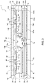
Figure 2 is a schematic cross-sectional view of the device illustrated inFigure 1 ; -
Figure 3 is a schematic top plan view, with portions removed, of a die of the device illustrated inFigures 1 and2 ; -
Figure 4 is a schematic perspective view of the die illustrated inFigure 3 ; -
Figure 5 is a schematic perspective view of a further embodiment of the present device; and -
Figure 6 is a schematic cross-sectional view of a further embodiment of the present device. -
Figure 1 shows a package 1 for asemiconductor device 2, in particular a bidirectional AC switch. As will be highlighted hereinafter, the package 1 is of the double island surface mount type. - In detail, the package 1 comprises a package coating 5 (illustrated in
Figure 2 , but not inFigure 1 ), made of insulating material (for example, an epoxy resin), and a first portion P1 and a second portion P2. Without this implying any loss of generality, the first and second portions PI, P2 are the same as one another and are arranged in a symmetrical way within thesemiconductor device 2, as on the other hand also are the first andsecond dice - In detail, the first portion P1 comprises a
support 4 of a leadframe 3, formed by a metal plate (for example, made of copper and with a parallelepipedal shape) and having atop surface 4a and abottom surface 4b. Thesupport 4, in itself known, is also referred to as "island" or die pad. - The
bottom surface 4b of thesupport 4 forms an exposedbottom surface 1b of the package 1 (illustrated inFigure 2 ), which can itself function as heat dissipater or be coupled (in a way not illustrated herein) to an external heat dissipater so as to increase the capacity of heat dissipation towards the outside. - The package coating 5, inter alia, englobes and coats at the top the support 4 (leaving the
bottom surface 4b thereof exposed, as mentioned previously), and alateral surface 4c. - The first portion P1 of the package 1 further comprises a
bottom insulation multilayer 26, arranged on top of thesupport 4. In particular, thebottom insulation multilayer 26 is a multilayer of the DBC (Direct Bonded Copper) type, and is hence formed by a respectivetop metal layer 26a and a respectivebottom metal layer 26b, both made of copper, as well as by a respectiveintermediate layer 26c made of ceramic material, for example alumina (Al2O3), or alternatively aluminium nitride (AlN) or beryllium oxide (BeO). Thetop metal layer 26a, thebottom metal layer 26b, and theintermediate layer 26c are arranged stacked on one another and are coupled together by means of direct eutectic bonding at high temperature; theintermediate layer 26c electrically insulates the top andbottom metal layers - The
bottom metal layer 26b is coupled to thetop surface 4a of thesupport 4, by means of a first layer ofsolder paste 7a (illustrated inFigure 2 ). - The
semiconductor device 2 further comprises afirst die 6 and asecond die 106, formed inside which are a first power MOSFET M1 and a second power MOSFET M2, respectively. Without this implying any loss of generality, the first andsecond dice semiconductor device 2. In what follows, for brevity, only thefirst die 6 is hence described. Moreover, the components of thesecond die 106 are designated by the same reference numbers as the components of thefirst die 6, increased by 10. In addition, the first andsecond dice first die 6 to the first portion P1 of the package 1 is described. In addition, it may be noted how inFigure 1 the first andsecond dice top insulation multilayer 16", described in what follows; for these details, as well as for the details regarding the first andsecond dice Figure 2 . - In detail, the
first die 6 is arranged on thebottom insulation multilayer 26 of the first portion P1 of the package 1. - In greater detail, the
first die 6 has afront surface 6a, arear surface 6b, and anintermediate surface 6c. Moreover, the first die 6 comprises abody 9 made of semiconductor material, for example silicon, integrated in which are, in a way in itself known and not illustrated in detail herein, a plurality of elementary units (or cells) of the first power MOSFET M1, arranged in stripes and having, for example, a vertical, columnar, structure, each cell being provided with a respective gate region and a respective source region. Thesemiconductor body 9 is delimited at the top by the aforementionedintermediate surface 6c and forms a drain region of the first power MOSFET M1. - In addition, the
first die 6 comprises adrain metallization 8, which is arranged underneath thesemiconductor body 9, in direct contact therewith, and forms therear surface 6b of thefirst die 6. Thedrain metallization 8 forms a drain pad of the first power MOSFET M1. In addition, thedrain metallization 8, and hence therear surface 6b of thefirst die 6, is coupled to thetop metal layer 26a of thebottom insulation multilayer 26 by interposition of a second layer ofsolder paste 7b. Thedrain metallization 8 is hence electrically and thermally connected to thetop metal layer 26a of theinsulation multilayer 26. Moreover, thedrain metallization 8 of the first power MOSFET M1 is electrically insulated from thesupport 4. - The first die 6 further comprises a
passivation region 13, which extends on thesemiconductor body 9 and forms the aforementionedtop surface 6a. In this connection, it should be noted how, as mentioned previously, inFigure 1 thefirst die 6 is illustrated as a whole, i.e., without illustrating, inter alia, thesemiconductor body 9, thepassivation region 13, and thecathode metallization 8. - As shown in greater detail in
Figure 3 (where, however, thepassivation region 13 is not illustrated, for greater clarity), the first die 6 comprises a number of gate-metallization lines 10 (the so-called "gate fingers"), which enable biasing (in a way not illustrated, but in itself known) of the gate regions of the cells of the first power MOSFET M1. In this connection, in the embodiment illustrated inFigure 3 just one gate-metallization line 10 is present, without this implying any loss of generality. - The gate-
metallization lines 10 extend underneath thepassivation region 13 and are parallel to one another. In addition, the gate-metallization lines 10 may be continuous or, as in the example illustrated, have interruptions along their longitudinal extension. In addition, the gate-metallization lines 10 delimit, in top plan view, portions 11 (illustrated only inFigure 3 ) of thepassivation region 13, which are referred to in what follows as "top passivation areas 11". - As illustrated in
Figure 4 , formed within thetop passivation areas 11 are corresponding windows 18 (illustrated inFigure 4 ), which extend within thepassivation region 13, starting from thetop surface 6a, for a depth such as to not penetrate into thesemiconductor body 9. In particular, eachwindow 18 is delimited laterally by two portions of the correspondingtop passivation area 11. - As may be seen in
Figures 2-4 , thefirst die 6 further comprises source contact regions 12 (also referred to as source pads), which are made of conductive material (for example, a metal), are in electrical contact with the source regions of the cells of the first power MOSFET M1 and are insulated from the aforesaid gate-metallization lines 10. In addition, eachsource contact region 12 delimits a correspondingwindow 18 at the bottom. - In the example illustrated, the
source contact regions 12 are rectangular in top plan view and moreover have dimensions that are the same as one another. In particular, present in thefirst die 6 are twotop passivation areas 11, present within which are twowindows 18, arranged inside which are correspondingsource contact regions 12. However, as mentioned previously, the distribution and number of the gate-metallization lines 10, of thetop passivation areas 11, and of thesource contact regions 12 may vary according to the characteristics and requirements of thepower semiconductor device 2. Moreover, assuming, in general, a succession of any number oftop passivation areas 11, the top initial and final passivation areas of the succession are delimited only on a respective side (in particular, the one facing the other top passivation areas) by a respective gate-metallization line 10. Consequently, considering each of the corresponding twowindows 18, one of the two portions of the correspondingtop passivation area 11 that delimit them (in particular, the portion facing outwards) does not contain any gate-metallization line. - As mentioned previously, the aforesaid
source contact regions 12 are arranged within thetop passivation areas 11, approximately at one and the same height with respect to the gate-metallization lines 10. Moreover, thesource contact regions 12 delimit the correspondingwindows 18 at the bottom. - Once again with reference to the gate-
metallization lines 10, each of them is overlaid by a corresponding portion 10' of thepassivation region 13, referred to in what follows as "corresponding main passivation portion 10'". In particular, each gate-metallization line 10 is coated with a corresponding main passivation portion 10'. - The
first die 6 further comprises one ormore gate pads 15, visible only inFigure 1 (where just one is illustrated, arranged approximately, and qualitatively, on the first die 6) and inFigure 4 . In particular, with reference toFigure 4 , for simplicity of representation, this shows thegate pad 15 as being arranged in contact with thesemiconductor body 9, even though in actual fact thegate pad 15 is arranged at a (short) distance from the latter. Eachgate pad 15 is electrically coupled to a corresponding gate-metallization line 10. In addition, thepassivation region 13 leaves thegate pads 15 exposed. Without this implying any loss of generality, in the example illustrated inFigures 1-4 , thefirst die 6 comprises just onegate pad 15. - Once again with reference to the first portion P1 of the package 1, it further comprises a
drain lead 27 and agate lead 29, which have, for example, the shape of parallelepipeds, are made of the same metal material as the one of which thesupport 4 is made and are physically separated from one another, as well as from thesupport 4. Thedrain lead 27 is connected to thetop metal layer 26a of theinsulation multilayer 26, and in particular to a portion of thetop metal layer 26a not overlaid by thefirst die 6, by means of a so-called clip 28 (illustrated inFigure 1 ) made of conductive material (for example, copper), referred to in what follows as "drain clip 28". In a way in itself known, thedrain clip 28 is connected at its ends to the aforementioned portion of thetop metal layer 26a and to thedrain lead 27, by means of corresponding areas of solder paste (not illustrated). - The
gate pad 15 of thefirst die 6 is connected to thegate lead 29 of the first portion P1 of the package 1 by means of a conductive wire 15', i.e., by means of wire bonding. - Once again with reference to the first portion P1 of the package 1, as may be seen in
Figure 5 , the corresponding drain leads 27 and gate leads 29 are exposed laterally and underneath; i.e., they are not coated with thecoating 5. In other words, assuming that thecoating 5 has an envelope shaped, for example, like a parallelepiped, the bottom and top bases of which are formed by thebottom surface 1b and by atop surface 1a, the drain leads 27 and gate leads 29 form a first lateral surface PW1 of said envelope, in addition to forming thebottom surface 1b. On the other hand, also the part of thesupport 4 is laterally exposed, since it gives out, for example, onto a second lateral surface PW2. Once again with reference toFigure 5 , it should be noted that, without this implying any loss of generality, it refers to an embodiment in which thesupport 4 has a shape different from a parallelepiped, since it includes a main body having a parallelepipedal shape and a plurality of protrusions, which branch off from one and the same lateral face of the main body, until they give out onto the aforementioned lateral surface PW2. - The package 1 further comprises a
source lead 31, which, as described in greater detail hereinafter, is shared between the first and second portions P1, P2 of the package 1. Also thecurrent lead 31 is exposed laterally and underneath. - The package 1 of the
power semiconductor device 2 further comprises (see once againFigures 1 and2 ) afurther insulation multilayer 16, referred to in what follows as "top insulation multilayer 16". - In detail, the
top insulation multilayer 16 is a DBC multilayer and includes a respectivetop metal layer 16a and a respectivebottom metal layer 16b, both made of copper, as well as a respective intermediate insulatinglayer 16c made of ceramic material, for example, the same material as the one of which the intermediate insulatinglayer 26c is made. The thicknesses of thetop metal layer 16a and of the intermediate insulatinglayer 16c may be equal, for example, to the thicknesses of the corresponding layers of thebottom insulation multilayer 26. The intermediate insulatinglayer 16c electrically insulates the top andbottom metal layers - The
top metal layer 16a of thetop insulation multilayer 16 forms a part of thetop surface 1a of the package 1, which can function itself as heat dissipater or be coupled (in a way not illustrated herein) to a further external heat dissipater so as to increase the capacity of heat dissipation outwards. - The
bottom metal layer 16b of thetop insulation multilayer 16 is shaped in a way corresponding to the conformation of the first andsecond dice bottom metal layer 16b comprises a firstperipheral portion 30 and a secondperipheral portion 130, and acentral portion 32. - The first and second
peripheral portions second dice peripheral portion 30 and thefirst die 6 is the same as the relative arrangement of the secondperipheral portion 130 and thesecond die 106. For this reason, described in what follows are only the firstperipheral portion 30 and corresponding coupling thereof to thefirst die 6. Moreover, the elements of the secondperipheral portion 130 are designated by the same reference numbers as the ones used for the firstperipheral portion 30, increased by 100. - In detail, the first
peripheral portion 30 of thebottom metal layer 16b has a shape that corresponds to the arrangement of the gate-metallization lines 10 of thefirst die 6, and more precisely to the arrangement of the corresponding main passivation portions 10', as well as to the arrangement of thesource contact regions 12. - In greater detail, and with reference to
Figure 2 , the firstperipheral portion 30 of thebottom metal layer 16b of thetop insulation multilayer 16 has a comb-like conformation. In fact, the firstperipheral portion 30 includes aplanar region 34 and a number ofcontact regions 36, which extend as bumps, starting from theplanar region 34, towards the underlyingfirst die 6. In particular, eachcontact region 36 extends until it penetrates into a correspondingwindow 18 of the underlyingfirst die 6, so as to couple mechanically and electrically to a correspondingsource contact region 12. For instance, eachcontact region 36 has a parallelepipedal shape and has a respective bottom plane surface, which mechanically and electrically couples to the correspondingsource contact region 12, by interposition of a corresponding solder-paste region 19. Moreover, eachcontact region 36 extends at a distance from the side walls of the correspondingwindow 18, so as not to contact the correspondingmain passivation area 11. - In turn, adjacent pairs of
contact regions 36 laterally delimit acorresponding insulation cavity 40, which is delimited at the top by a corresponding part of theplanar region 34 and is open at the bottom. The insulation cavities 40 are hence trenches (for example, with rectangular cross section, invariant for translations parallel to the direction of extension of the gate-metallization lines 10) interposed between thecontact regions 36, so as to overlie, at a distance, corresponding gate-metallization lines 10. The top wall of each trench is formed by theplanar region 34, whereas the side walls are formed by the correspondingcontact regions 36. Present inFigure 2 is just oneinsulation cavity 40, because it is assumed, purely by way of example, that thefirst die 6 comprises just twosource contact regions 12 and just one gate-metallization line 10. However, it is evident how the number, shape, and arrangement of theinsulation cavities 40 may differ, according to the arrangement and conformation of the gate-metallization lines 10 and of thesource contact regions 12. - In practice, the
insulation cavities 40 are laterally staggered with respect to thewindows 18, with respect to which they are moreover arranged at a greater height. In addition, theinsulation cavities 40 and thewindows 18 have opposite concavities; i.e., theinsulation cavities 40 are open downwards, whereas thewindows 18 are open upwards. - In greater detail, each
insulation cavity 40 overlies a corresponding main passivation portion 10', which, as has been said, in turn overlies a corresponding gate-metallization line 10 and projects from theadjacent windows 18, towards therespective insulation cavity 40. Without this implying any loss of generality, the projection of each main passivation portion 10' is such that the point of maximum height is to a first approximation arranged above the underlying gate-metallization line 10. - In particular, each main passivation portion 10' is set at a distance from the
respective insulation cavity 40; i.e., it does not contact either the top wall or the side walls of thecorresponding insulation cavity 40, even though it can penetrate at least in part into the correspondinginsulation cavity 40, and more precisely into the volume delimited by the latter; in other words, present between each main passivation portion 10' and thecorresponding insulation cavity 40 is a gap that prevents contact between the main passivation portion 10' and the side and top walls of theinsulation cavity 40. In this way, thecontact regions 36 straddle or by-pass the main passivation portions 10', since they are laterally interspersed with the latter. Thus thecontact regions 36, which enable contacting of thesource contact regions 12, are prevented from damaging the main passivation portions 10' and the underlying gate-metallization lines 10. - As regards the
central portion 32 of thebottom metal layer 16b of thetop insulation multilayer 16, it connects theplanar regions peripheral portions bottom metal layer 16b, to form a single piece with the latter. Theplanar regions central portion 32 form a layered region that may have a thickness, for example, equal to the thickness of thebottom metal layer 26b of thebottom insulation multilayer 26. - As may be seen in
Figure 1 , a bottom portion of thecentral portion 32 of thebottom metal layer 16b moreover forms a main portion 14' of asource clip 14. Thissource clip 14 further comprises a connectingportion 14", which connects the aforesaid main portion 14' to thesource lead 31. This connectingportion 14" may be provided integrally with the main portion 14', and hence with thecentral portion 32 of thebottom metal layer 16b. Variants are in any case possible, in which, for example, thesource clip 14 does not form a single piece with thebottom metal layer 16b, but is coupled to the latter by interposition of a corresponding area of solder paste. - In practice, the
bottom metal layer 16b of thetop insulation multilayer 16 shorts the source terminals of the first and second power MOSFETs M1, M2, thus forming a node electrically accessible via thesource lead 31. The drain and gate terminals of the first power MOSFET M1 are, instead, accessible via thedrain lead 27 and thegate lead 29, respectively; the drain and gate terminals of the second power MOSFET M2 are instead accessible via thedrain lead 127 and thegate lead 129, respectively. - The advantages of the solution disclosed emerge in clearly from what has been described above.
- In particular, in terms of encumbrance, the present power device makes it possible to benefit from the advantages deriving from a package of the surface mount type, albeit guaranteeing good electrical insulation and a considerable heat-dissipation capacity.
- In particular, the present package may have a maximum thickness in a vertical direction in the region of 2-3 mm. Moreover, the package affords the possibility of cooling on both sides (both top and bottom). Once again, the presence of the top insulation multilayer in bridge configuration, i.e., which extends so as to overlie both of the dice, guarantees a considerable thermal efficiency, reduced parasitic packaging electrical effects (in particular, inductive effects) and a low contact resistance. Once again, the connections to the source regions of the power MOSFETs do not require the use of wire bonding.
- In particular, as regards thermal dissipation, the fact that the
top metal layer 16a is insulated from the source regions of the first and second power MOSFETs M1 and M2 means that it can be sized freely so as to optimise the power dissipation, without constraints due to the need to guarantee a certain flow of current. In this connection, the thickness of thebottom metal layer 16b can be sized so that the flow of current is limited not by this, but rather by the drain clips 28 and 128. - In addition, with reference, for example, to the first portion P1 of the package 1, the presence of the
top metal layer 26a of thebottom insulation multilayer 26 makes it possible to have an optimal coupling area for thedrain clip 28. Moreover, the fact that the leadframe supports are insulated from the drain regions of the first and second power MOSFETs M1 and M2 means that they are at one and the same potential. Consequently, the leadframe supports can be arranged very close to one another, with consequent reduction of the vertical encumbrance of the package 1. - Finally, it is clear that modifications and variations may be made to what has been described and illustrated herein, without thereby departing from the sphere of protection of the present invention, as defined in the annexed claims.
- The metal layers of the insulation multilayer may be made of metal materials other than copper.
- The clip connections may be replaced by corresponding wire bonds, even though the clips guarantee a greater drawing-off of heat and the capacity of being traversed by higher currents.
- The shape of the support of the leadframe may be different from what has been described; for example, it may include a pair of planar subregions connected together and vertically staggered with respect to one another.
- The gate, source, and drain leads, as well as the portions of the support that gives out on the outside of the package may protrude with respect to the envelope of the package, instead of being flush with the respective walls of the package.
- As regards each of the first and second peripheral portions of the bottom metal layer of the top insulation multilayer, the corresponding contact regions may be distributed in a way different from what has been described. In addition, each one of the aforementioned first and second peripheral portions may include a respective planar subportion, without contact regions.
- Moreover possible are embodiments of the type illustrated in
Figure 6 , in which thetop metal layer 16a and theintermediate layer 16c of thetop insulation multilayer 16 are absent. In this case, thebottom metal layer 16b forms part of thetop surface 1a of the package 1. - Finally, corresponding semiconductor devices other than MOSFETs, such as, purely by way of example, IGBTs, may be integrated in the dice. The present package makes it, in fact, possible to manage the coupling between the top insulation multilayer and any semiconductor device, present in which are passivation regions overlying metallization lines arranged on the semiconductor body of the corresponding die and interposed between contact regions that are to be biased.
Claims (10)
- A power semiconductor device (2) comprising:- a first die (6) and a second die (106), each of which comprises a plurality of conductive contact regions (12) and a passivation region (13), which includes a number of projecting dielectric regions (10') and a number of windows (18, 118), adjacent windows being separated by a corresponding projecting dielectric region, each conductive contact region being arranged within a corresponding window; and- a package (1) of the surface mount type, housing the first and second dice;and wherein the package comprises:- a first bottom insulation multilayer (26) and a second bottom insulation multilayer (126), which carry, respectively, the first and second dice and each include a respective top metal layer (26a, 126a), a respective bottom metal layer (26b, 126b) and a respective intermediate insulating layer (26c, 126c), interposed between the corresponding top metal layer and the corresponding bottom metal layer; and- a covering metal layer (16b), arranged on top of the first and second dice and comprising projecting metal regions (36), which extend into the windows so as to couple electrically with corresponding conductive contact regions, said covering metal layer moreover forming a number of cavities (40), interposed between the projecting metal regions so as to overlie corresponding projecting dielectric regions.
- The device according to claim 1, further comprising a top insulation multilayer (16) formed by a respective top metal layer (16a), by said covering metal layer (16b), and by a respective intermediate insulating layer (16c), which is interposed between said respective top metal layer and said covering metal layer.
- The device according to claim 1 or claim 2, further comprising a first support (4) and a second support (104) made of metal material, which carry, respectively, the first and second bottom insulation multilayers (26, 126).
- The device according to any one of the preceding claims, wherein said package (1) further comprises:- a package coating (5), which covers the first and second dice (6, 106) and the first and second bottom insulation multilayers (26, 126); and- a first lead (31), which comprises a part left exposed from the package coating;and wherein the covering metal layer (16b) is electrically coupled to the first lead (31).
- The device according to claim 4 when depending upon Claim 3, wherein the package coating (5) moreover covers the first and second supports (4, 104); and wherein each one of the first and second supports comprises a respective portion left exposed from the package coating.
- The device according to claim 4 or claim 5, wherein the package (1) further comprises a second lead (27) and a third lead (127), each of which comprises a respective portion left exposed from the package coating (5); and wherein the top metal layers (26a, 126a) of the first and second bottom insulation multilayers (26, 126) are electrically coupled, respectively, to the second and third leads.
- The device according to any one of the preceding claims, wherein each one of the first and second dice (6, 106) comprises a number of metallization lines (10), each of which is coated with a corresponding dielectric projecting region (10').
- The device according to claim 7, wherein the first and second dice (6, 106) form, respectively, a first transistor (M1) and a second transistor (M2); and wherein said metallization lines (10) of the first and second dice are gate lines of the respective transistor; and wherein said conductive contact regions (12) of the first and second dice are source contact regions of the respective transistor.
- The device according to any one of the preceding claims, wherein each one of the first and second dice (6, 106) comprises a respective bottom-contact metallization (8, 108); and wherein the bottom-contact metallizations of the first and second dice are electrically coupled to the top metal layer (26a, 126a) of the first and second bottom insulation multilayers (26, 126), respectively.
- The device according to any one of the preceding claims, wherein said covering-metal layer (16b) extends at a distance from the passivation regions (13) of the first and second dice (6, 106).
Applications Claiming Priority (1)
| Application Number | Priority Date | Filing Date | Title |
|---|---|---|---|
| IT102018000004782A IT201800004782A1 (en) | 2018-04-23 | 2018-04-23 | SEMICONDUCTOR POWER DEVICE WITH SURFACE MOUNT ENCAPSULATION WITH DOUBLE ISLAND |
Publications (2)
| Publication Number | Publication Date |
|---|---|
| EP3561867A1 true EP3561867A1 (en) | 2019-10-30 |
| EP3561867B1 EP3561867B1 (en) | 2024-02-14 |
Family
ID=62751489
Family Applications (1)
| Application Number | Title | Priority Date | Filing Date |
|---|---|---|---|
| EP19165579.4A Active EP3561867B1 (en) | 2018-04-23 | 2019-03-27 | A power semiconductor device with a double island surface mount package |
Country Status (4)
| Country | Link |
|---|---|
| US (4) | US10910302B2 (en) |
| EP (1) | EP3561867B1 (en) |
| CN (2) | CN110391195A (en) |
| IT (1) | IT201800004782A1 (en) |
Cited By (2)
| Publication number | Priority date | Publication date | Assignee | Title |
|---|---|---|---|---|
| EP3944309A1 (en) * | 2020-07-10 | 2022-01-26 | STMicroelectronics S.r.l. | Packaged high voltage mosfet device with a dbc interconnection substrate and manufacturing process thereof |
| IT202400009481A1 (en) * | 2024-04-24 | 2025-10-24 | St Microelectronics Int Nv | ENCAPSULATED ELECTRONIC DEVICE COMPRISING CIRCUITS FORMED BY A MULTIPLE POWER DEVICES COUPLED IN A SOURCE-TO-SOURCE OR DRAIN-TO-DRAIN CONFIGURATION |
Families Citing this family (6)
| Publication number | Priority date | Publication date | Assignee | Title |
|---|---|---|---|---|
| IT201800004782A1 (en) | 2018-04-23 | 2019-10-23 | SEMICONDUCTOR POWER DEVICE WITH SURFACE MOUNT ENCAPSULATION WITH DOUBLE ISLAND | |
| US11088083B2 (en) * | 2018-06-29 | 2021-08-10 | Taiwan Semiconductor Manufacturing Company, Ltd. | DC and AC magnetic field protection for MRAM device using magnetic-field-shielding structure |
| US12132010B2 (en) * | 2021-04-08 | 2024-10-29 | GM Global Technology Operations LLC | Metal-coated, polymer-encapsulated electronics modules and methods for making the same |
| JP7519956B2 (en) * | 2021-05-28 | 2024-07-22 | 三菱電機株式会社 | SWITCHING DEVICE, SEMICONDUCTOR DEVICE, AND METHOD FOR MANUFACTURING SWITCHING DEVICE |
| EP4333030A1 (en) * | 2022-08-31 | 2024-03-06 | Nexperia B.V. | Electronic package and manufacturing method therefor |
| IT202300024267A1 (en) | 2023-11-16 | 2025-05-16 | St Microelectronics Int Nv | HIGH THERMAL DISSIPATION ENCAPSULATED ELECTRONIC DEVICE COMPRISING A PLURALITY OF POWER TRANSISTORS AND RELATED MANUFACTURING PROCEDURE |
Citations (4)
| Publication number | Priority date | Publication date | Assignee | Title |
|---|---|---|---|---|
| US20090079006A1 (en) * | 2007-09-25 | 2009-03-26 | Kabushiki Kaisha Toshiba | Semiconductor apparatus |
| US20130161801A1 (en) * | 2011-12-23 | 2013-06-27 | Infineon Technologies Ag | Module Including a Discrete Device Mounted on a DCB Substrate |
| EP2804212A1 (en) * | 2012-03-28 | 2014-11-19 | Fuji Electric Co., Ltd. | Semiconductor device |
| WO2017157486A1 (en) * | 2016-03-16 | 2017-09-21 | Abb Schweiz Ag | Semiconductor device |
Family Cites Families (6)
| Publication number | Priority date | Publication date | Assignee | Title |
|---|---|---|---|---|
| US7479691B2 (en) * | 2005-03-16 | 2009-01-20 | Infineon Technologies Ag | Power semiconductor module having surface-mountable flat external contacts and method for producing the same |
| JP5561922B2 (en) * | 2008-05-20 | 2014-07-30 | 三菱電機株式会社 | Power semiconductor device |
| US8354740B2 (en) * | 2008-12-01 | 2013-01-15 | Alpha & Omega Semiconductor, Inc. | Top-side cooled semiconductor package with stacked interconnection plates and method |
| JP2013021254A (en) * | 2011-07-14 | 2013-01-31 | Mitsubishi Electric Corp | Semiconductor device and manufacturing method of the same |
| US20150076676A1 (en) * | 2013-09-17 | 2015-03-19 | Jun Lu | Power semiconductor device package and fabrication method |
| IT201800004782A1 (en) | 2018-04-23 | 2019-10-23 | SEMICONDUCTOR POWER DEVICE WITH SURFACE MOUNT ENCAPSULATION WITH DOUBLE ISLAND |
-
2018
- 2018-04-23 IT IT102018000004782A patent/IT201800004782A1/en unknown
-
2019
- 2019-03-27 EP EP19165579.4A patent/EP3561867B1/en active Active
- 2019-04-09 CN CN201910279496.3A patent/CN110391195A/en active Pending
- 2019-04-09 CN CN201920468185.7U patent/CN209896058U/en active Active
- 2019-04-16 US US16/385,928 patent/US10910302B2/en active Active
-
2021
- 2021-01-06 US US17/142,738 patent/US11658108B2/en active Active
-
2023
- 2023-04-24 US US18/306,119 patent/US12278174B2/en active Active
-
2025
- 2025-04-11 US US19/177,400 patent/US20250391761A1/en active Pending
Patent Citations (4)
| Publication number | Priority date | Publication date | Assignee | Title |
|---|---|---|---|---|
| US20090079006A1 (en) * | 2007-09-25 | 2009-03-26 | Kabushiki Kaisha Toshiba | Semiconductor apparatus |
| US20130161801A1 (en) * | 2011-12-23 | 2013-06-27 | Infineon Technologies Ag | Module Including a Discrete Device Mounted on a DCB Substrate |
| EP2804212A1 (en) * | 2012-03-28 | 2014-11-19 | Fuji Electric Co., Ltd. | Semiconductor device |
| WO2017157486A1 (en) * | 2016-03-16 | 2017-09-21 | Abb Schweiz Ag | Semiconductor device |
Cited By (4)
| Publication number | Priority date | Publication date | Assignee | Title |
|---|---|---|---|---|
| EP3944309A1 (en) * | 2020-07-10 | 2022-01-26 | STMicroelectronics S.r.l. | Packaged high voltage mosfet device with a dbc interconnection substrate and manufacturing process thereof |
| US11830794B2 (en) | 2020-07-10 | 2023-11-28 | Stmicroelectronics S.R.L. | Packaged high voltage MOSFET device with connection clip and manufacturing process thereof |
| US12610832B2 (en) | 2020-07-10 | 2026-04-21 | Stmicroelectronics S.R.L. | Packaged high voltage MOSFET device with connection clip and manufacturing process thereof |
| IT202400009481A1 (en) * | 2024-04-24 | 2025-10-24 | St Microelectronics Int Nv | ENCAPSULATED ELECTRONIC DEVICE COMPRISING CIRCUITS FORMED BY A MULTIPLE POWER DEVICES COUPLED IN A SOURCE-TO-SOURCE OR DRAIN-TO-DRAIN CONFIGURATION |
Also Published As
| Publication number | Publication date |
|---|---|
| US20230282564A1 (en) | 2023-09-07 |
| US20210159161A1 (en) | 2021-05-27 |
| US20250391761A1 (en) | 2025-12-25 |
| CN110391195A (en) | 2019-10-29 |
| US11658108B2 (en) | 2023-05-23 |
| EP3561867B1 (en) | 2024-02-14 |
| CN209896058U (en) | 2020-01-03 |
| US20190326208A1 (en) | 2019-10-24 |
| US12278174B2 (en) | 2025-04-15 |
| US10910302B2 (en) | 2021-02-02 |
| IT201800004782A1 (en) | 2019-10-23 |
Similar Documents
| Publication | Publication Date | Title |
|---|---|---|
| US12278174B2 (en) | Power semiconductor device with a double island surface mount package | |
| US11239132B2 (en) | Semiconductor power device with corresponding package and related manufacturing process | |
| US10070528B2 (en) | Semiconductor device wiring pattern and connections | |
| US7227259B2 (en) | Low-inductance circuit arrangement for power semiconductor modules | |
| US9966344B2 (en) | Semiconductor device with separated main terminals | |
| CN100392856C (en) | power semiconductor module | |
| US11894290B2 (en) | Packaged stackable electronic power device for surface mounting and circuit arrangement | |
| KR20070081744A (en) | Pressurized Contact Power Semiconductor Modules | |
| US20070108575A1 (en) | Semiconductor package that includes stacked semiconductor die | |
| US12610832B2 (en) | Packaged high voltage MOSFET device with connection clip and manufacturing process thereof | |
| US11923266B2 (en) | Semiconductor module circuit structure | |
| JP2002151691A (en) | Low inductance circuit device | |
| JP2022130754A (en) | Semiconductor device | |
| JP2025138474A (en) | Semiconductor Devices |
Legal Events
| Date | Code | Title | Description |
|---|---|---|---|
| PUAI | Public reference made under article 153(3) epc to a published international application that has entered the european phase |
Free format text: ORIGINAL CODE: 0009012 |
|
| STAA | Information on the status of an ep patent application or granted ep patent |
Free format text: STATUS: THE APPLICATION HAS BEEN PUBLISHED |
|
| AK | Designated contracting states |
Kind code of ref document: A1 Designated state(s): AL AT BE BG CH CY CZ DE DK EE ES FI FR GB GR HR HU IE IS IT LI LT LU LV MC MK MT NL NO PL PT RO RS SE SI SK SM TR |
|
| AX | Request for extension of the european patent |
Extension state: BA ME |
|
| STAA | Information on the status of an ep patent application or granted ep patent |
Free format text: STATUS: REQUEST FOR EXAMINATION WAS MADE |
|
| 17P | Request for examination filed |
Effective date: 20200429 |
|
| RBV | Designated contracting states (corrected) |
Designated state(s): AL AT BE BG CH CY CZ DE DK EE ES FI FR GB GR HR HU IE IS IT LI LT LU LV MC MK MT NL NO PL PT RO RS SE SI SK SM TR |
|
| GRAP | Despatch of communication of intention to grant a patent |
Free format text: ORIGINAL CODE: EPIDOSNIGR1 |
|
| STAA | Information on the status of an ep patent application or granted ep patent |
Free format text: STATUS: GRANT OF PATENT IS INTENDED |
|
| INTG | Intention to grant announced |
Effective date: 20230322 |
|
| GRAJ | Information related to disapproval of communication of intention to grant by the applicant or resumption of examination proceedings by the epo deleted |
Free format text: ORIGINAL CODE: EPIDOSDIGR1 |
|
| STAA | Information on the status of an ep patent application or granted ep patent |
Free format text: STATUS: REQUEST FOR EXAMINATION WAS MADE |
|
| INTC | Intention to grant announced (deleted) | ||
| GRAP | Despatch of communication of intention to grant a patent |
Free format text: ORIGINAL CODE: EPIDOSNIGR1 |
|
| STAA | Information on the status of an ep patent application or granted ep patent |
Free format text: STATUS: GRANT OF PATENT IS INTENDED |
|
| INTG | Intention to grant announced |
Effective date: 20230905 |
|
| GRAS | Grant fee paid |
Free format text: ORIGINAL CODE: EPIDOSNIGR3 |
|
| GRAA | (expected) grant |
Free format text: ORIGINAL CODE: 0009210 |
|
| STAA | Information on the status of an ep patent application or granted ep patent |
Free format text: STATUS: THE PATENT HAS BEEN GRANTED |
|
| AK | Designated contracting states |
Kind code of ref document: B1 Designated state(s): AL AT BE BG CH CY CZ DE DK EE ES FI FR GB GR HR HU IE IS IT LI LT LU LV MC MK MT NL NO PL PT RO RS SE SI SK SM TR |
|
| REG | Reference to a national code |
Ref country code: GB Ref legal event code: FG4D |
|
| REG | Reference to a national code |
Ref country code: CH Ref legal event code: EP |
|
| REG | Reference to a national code |
Ref country code: DE Ref legal event code: R096 Ref document number: 602019046387 Country of ref document: DE |
|
| REG | Reference to a national code |
Ref country code: IE Ref legal event code: FG4D |
|
| REG | Reference to a national code |
Ref country code: LT Ref legal event code: MG9D |
|
| REG | Reference to a national code |
Ref country code: NL Ref legal event code: MP Effective date: 20240214 |
|
| PG25 | Lapsed in a contracting state [announced via postgrant information from national office to epo] |
Ref country code: IS Free format text: LAPSE BECAUSE OF FAILURE TO SUBMIT A TRANSLATION OF THE DESCRIPTION OR TO PAY THE FEE WITHIN THE PRESCRIBED TIME-LIMIT Effective date: 20240614 |
|
| PG25 | Lapsed in a contracting state [announced via postgrant information from national office to epo] |
Ref country code: LT Free format text: LAPSE BECAUSE OF FAILURE TO SUBMIT A TRANSLATION OF THE DESCRIPTION OR TO PAY THE FEE WITHIN THE PRESCRIBED TIME-LIMIT Effective date: 20240214 |
|
| PG25 | Lapsed in a contracting state [announced via postgrant information from national office to epo] |
Ref country code: GR Free format text: LAPSE BECAUSE OF FAILURE TO SUBMIT A TRANSLATION OF THE DESCRIPTION OR TO PAY THE FEE WITHIN THE PRESCRIBED TIME-LIMIT Effective date: 20240515 |
|
| REG | Reference to a national code |
Ref country code: AT Ref legal event code: MK05 Ref document number: 1657803 Country of ref document: AT Kind code of ref document: T Effective date: 20240214 |
|
| PG25 | Lapsed in a contracting state [announced via postgrant information from national office to epo] |
Ref country code: NL Free format text: LAPSE BECAUSE OF FAILURE TO SUBMIT A TRANSLATION OF THE DESCRIPTION OR TO PAY THE FEE WITHIN THE PRESCRIBED TIME-LIMIT Effective date: 20240214 Ref country code: RS Free format text: LAPSE BECAUSE OF FAILURE TO SUBMIT A TRANSLATION OF THE DESCRIPTION OR TO PAY THE FEE WITHIN THE PRESCRIBED TIME-LIMIT Effective date: 20240514 Ref country code: HR Free format text: LAPSE BECAUSE OF FAILURE TO SUBMIT A TRANSLATION OF THE DESCRIPTION OR TO PAY THE FEE WITHIN THE PRESCRIBED TIME-LIMIT Effective date: 20240214 |
|
| PG25 | Lapsed in a contracting state [announced via postgrant information from national office to epo] |
Ref country code: ES Free format text: LAPSE BECAUSE OF FAILURE TO SUBMIT A TRANSLATION OF THE DESCRIPTION OR TO PAY THE FEE WITHIN THE PRESCRIBED TIME-LIMIT Effective date: 20240214 |
|
| PG25 | Lapsed in a contracting state [announced via postgrant information from national office to epo] |
Ref country code: AT Free format text: LAPSE BECAUSE OF FAILURE TO SUBMIT A TRANSLATION OF THE DESCRIPTION OR TO PAY THE FEE WITHIN THE PRESCRIBED TIME-LIMIT Effective date: 20240214 |
|
| PG25 | Lapsed in a contracting state [announced via postgrant information from national office to epo] |
Ref country code: RS Free format text: LAPSE BECAUSE OF FAILURE TO SUBMIT A TRANSLATION OF THE DESCRIPTION OR TO PAY THE FEE WITHIN THE PRESCRIBED TIME-LIMIT Effective date: 20240514 Ref country code: NO Free format text: LAPSE BECAUSE OF FAILURE TO SUBMIT A TRANSLATION OF THE DESCRIPTION OR TO PAY THE FEE WITHIN THE PRESCRIBED TIME-LIMIT Effective date: 20240514 Ref country code: NL Free format text: LAPSE BECAUSE OF FAILURE TO SUBMIT A TRANSLATION OF THE DESCRIPTION OR TO PAY THE FEE WITHIN THE PRESCRIBED TIME-LIMIT Effective date: 20240214 Ref country code: LT Free format text: LAPSE BECAUSE OF FAILURE TO SUBMIT A TRANSLATION OF THE DESCRIPTION OR TO PAY THE FEE WITHIN THE PRESCRIBED TIME-LIMIT Effective date: 20240214 Ref country code: IS Free format text: LAPSE BECAUSE OF FAILURE TO SUBMIT A TRANSLATION OF THE DESCRIPTION OR TO PAY THE FEE WITHIN THE PRESCRIBED TIME-LIMIT Effective date: 20240614 Ref country code: HR Free format text: LAPSE BECAUSE OF FAILURE TO SUBMIT A TRANSLATION OF THE DESCRIPTION OR TO PAY THE FEE WITHIN THE PRESCRIBED TIME-LIMIT Effective date: 20240214 Ref country code: GR Free format text: LAPSE BECAUSE OF FAILURE TO SUBMIT A TRANSLATION OF THE DESCRIPTION OR TO PAY THE FEE WITHIN THE PRESCRIBED TIME-LIMIT Effective date: 20240515 Ref country code: FI Free format text: LAPSE BECAUSE OF FAILURE TO SUBMIT A TRANSLATION OF THE DESCRIPTION OR TO PAY THE FEE WITHIN THE PRESCRIBED TIME-LIMIT Effective date: 20240214 Ref country code: ES Free format text: LAPSE BECAUSE OF FAILURE TO SUBMIT A TRANSLATION OF THE DESCRIPTION OR TO PAY THE FEE WITHIN THE PRESCRIBED TIME-LIMIT Effective date: 20240214 Ref country code: BG Free format text: LAPSE BECAUSE OF FAILURE TO SUBMIT A TRANSLATION OF THE DESCRIPTION OR TO PAY THE FEE WITHIN THE PRESCRIBED TIME-LIMIT Effective date: 20240214 Ref country code: AT Free format text: LAPSE BECAUSE OF FAILURE TO SUBMIT A TRANSLATION OF THE DESCRIPTION OR TO PAY THE FEE WITHIN THE PRESCRIBED TIME-LIMIT Effective date: 20240214 |
|
| PG25 | Lapsed in a contracting state [announced via postgrant information from national office to epo] |
Ref country code: PL Free format text: LAPSE BECAUSE OF FAILURE TO SUBMIT A TRANSLATION OF THE DESCRIPTION OR TO PAY THE FEE WITHIN THE PRESCRIBED TIME-LIMIT Effective date: 20240214 Ref country code: PT Free format text: LAPSE BECAUSE OF FAILURE TO SUBMIT A TRANSLATION OF THE DESCRIPTION OR TO PAY THE FEE WITHIN THE PRESCRIBED TIME-LIMIT Effective date: 20240614 |
|
| PG25 | Lapsed in a contracting state [announced via postgrant information from national office to epo] |
Ref country code: SE Free format text: LAPSE BECAUSE OF FAILURE TO SUBMIT A TRANSLATION OF THE DESCRIPTION OR TO PAY THE FEE WITHIN THE PRESCRIBED TIME-LIMIT Effective date: 20240214 Ref country code: PT Free format text: LAPSE BECAUSE OF FAILURE TO SUBMIT A TRANSLATION OF THE DESCRIPTION OR TO PAY THE FEE WITHIN THE PRESCRIBED TIME-LIMIT Effective date: 20240614 Ref country code: PL Free format text: LAPSE BECAUSE OF FAILURE TO SUBMIT A TRANSLATION OF THE DESCRIPTION OR TO PAY THE FEE WITHIN THE PRESCRIBED TIME-LIMIT Effective date: 20240214 Ref country code: LV Free format text: LAPSE BECAUSE OF FAILURE TO SUBMIT A TRANSLATION OF THE DESCRIPTION OR TO PAY THE FEE WITHIN THE PRESCRIBED TIME-LIMIT Effective date: 20240214 |
|
| PG25 | Lapsed in a contracting state [announced via postgrant information from national office to epo] |
Ref country code: DK Free format text: LAPSE BECAUSE OF FAILURE TO SUBMIT A TRANSLATION OF THE DESCRIPTION OR TO PAY THE FEE WITHIN THE PRESCRIBED TIME-LIMIT Effective date: 20240214 |
|
| PG25 | Lapsed in a contracting state [announced via postgrant information from national office to epo] |
Ref country code: SM Free format text: LAPSE BECAUSE OF FAILURE TO SUBMIT A TRANSLATION OF THE DESCRIPTION OR TO PAY THE FEE WITHIN THE PRESCRIBED TIME-LIMIT Effective date: 20240214 |
|
| PG25 | Lapsed in a contracting state [announced via postgrant information from national office to epo] |
Ref country code: EE Free format text: LAPSE BECAUSE OF FAILURE TO SUBMIT A TRANSLATION OF THE DESCRIPTION OR TO PAY THE FEE WITHIN THE PRESCRIBED TIME-LIMIT Effective date: 20240214 Ref country code: CZ Free format text: LAPSE BECAUSE OF FAILURE TO SUBMIT A TRANSLATION OF THE DESCRIPTION OR TO PAY THE FEE WITHIN THE PRESCRIBED TIME-LIMIT Effective date: 20240214 |
|
| PG25 | Lapsed in a contracting state [announced via postgrant information from national office to epo] |
Ref country code: SK Free format text: LAPSE BECAUSE OF FAILURE TO SUBMIT A TRANSLATION OF THE DESCRIPTION OR TO PAY THE FEE WITHIN THE PRESCRIBED TIME-LIMIT Effective date: 20240214 |
|
| PG25 | Lapsed in a contracting state [announced via postgrant information from national office to epo] |
Ref country code: SM Free format text: LAPSE BECAUSE OF FAILURE TO SUBMIT A TRANSLATION OF THE DESCRIPTION OR TO PAY THE FEE WITHIN THE PRESCRIBED TIME-LIMIT Effective date: 20240214 Ref country code: SK Free format text: LAPSE BECAUSE OF FAILURE TO SUBMIT A TRANSLATION OF THE DESCRIPTION OR TO PAY THE FEE WITHIN THE PRESCRIBED TIME-LIMIT Effective date: 20240214 Ref country code: RO Free format text: LAPSE BECAUSE OF FAILURE TO SUBMIT A TRANSLATION OF THE DESCRIPTION OR TO PAY THE FEE WITHIN THE PRESCRIBED TIME-LIMIT Effective date: 20240214 Ref country code: EE Free format text: LAPSE BECAUSE OF FAILURE TO SUBMIT A TRANSLATION OF THE DESCRIPTION OR TO PAY THE FEE WITHIN THE PRESCRIBED TIME-LIMIT Effective date: 20240214 Ref country code: DK Free format text: LAPSE BECAUSE OF FAILURE TO SUBMIT A TRANSLATION OF THE DESCRIPTION OR TO PAY THE FEE WITHIN THE PRESCRIBED TIME-LIMIT Effective date: 20240214 Ref country code: CZ Free format text: LAPSE BECAUSE OF FAILURE TO SUBMIT A TRANSLATION OF THE DESCRIPTION OR TO PAY THE FEE WITHIN THE PRESCRIBED TIME-LIMIT Effective date: 20240214 |
|
| REG | Reference to a national code |
Ref country code: CH Ref legal event code: PL |
|
| REG | Reference to a national code |
Ref country code: DE Ref legal event code: R097 Ref document number: 602019046387 Country of ref document: DE |
|
| PG25 | Lapsed in a contracting state [announced via postgrant information from national office to epo] |
Ref country code: LU Free format text: LAPSE BECAUSE OF NON-PAYMENT OF DUE FEES Effective date: 20240327 |
|
| PG25 | Lapsed in a contracting state [announced via postgrant information from national office to epo] |
Ref country code: MC Free format text: LAPSE BECAUSE OF FAILURE TO SUBMIT A TRANSLATION OF THE DESCRIPTION OR TO PAY THE FEE WITHIN THE PRESCRIBED TIME-LIMIT Effective date: 20240214 |
|
| PG25 | Lapsed in a contracting state [announced via postgrant information from national office to epo] |
Ref country code: MC Free format text: LAPSE BECAUSE OF FAILURE TO SUBMIT A TRANSLATION OF THE DESCRIPTION OR TO PAY THE FEE WITHIN THE PRESCRIBED TIME-LIMIT Effective date: 20240214 Ref country code: LU Free format text: LAPSE BECAUSE OF NON-PAYMENT OF DUE FEES Effective date: 20240327 |
|
| PG25 | Lapsed in a contracting state [announced via postgrant information from national office to epo] |
Ref country code: IT Free format text: LAPSE BECAUSE OF FAILURE TO SUBMIT A TRANSLATION OF THE DESCRIPTION OR TO PAY THE FEE WITHIN THE PRESCRIBED TIME-LIMIT Effective date: 20240214 |
|
| REG | Reference to a national code |
Ref country code: BE Ref legal event code: MM Effective date: 20240331 |
|
| PLBE | No opposition filed within time limit |
Free format text: ORIGINAL CODE: 0009261 |
|
| STAA | Information on the status of an ep patent application or granted ep patent |
Free format text: STATUS: NO OPPOSITION FILED WITHIN TIME LIMIT |
|
| PG25 | Lapsed in a contracting state [announced via postgrant information from national office to epo] |
Ref country code: IT Free format text: LAPSE BECAUSE OF FAILURE TO SUBMIT A TRANSLATION OF THE DESCRIPTION OR TO PAY THE FEE WITHIN THE PRESCRIBED TIME-LIMIT Effective date: 20240214 |
|
| PG25 | Lapsed in a contracting state [announced via postgrant information from national office to epo] |
Ref country code: BE Free format text: LAPSE BECAUSE OF NON-PAYMENT OF DUE FEES Effective date: 20240331 |
|
| PG25 | Lapsed in a contracting state [announced via postgrant information from national office to epo] |
Ref country code: FR Free format text: LAPSE BECAUSE OF NON-PAYMENT OF DUE FEES Effective date: 20240414 |
|
| 26N | No opposition filed |
Effective date: 20241115 |
|
| PG25 | Lapsed in a contracting state [announced via postgrant information from national office to epo] |
Ref country code: IE Free format text: LAPSE BECAUSE OF NON-PAYMENT OF DUE FEES Effective date: 20240327 |
|
| GBPC | Gb: european patent ceased through non-payment of renewal fee |
Effective date: 20240514 |
|
| PG25 | Lapsed in a contracting state [announced via postgrant information from national office to epo] |
Ref country code: IE Free format text: LAPSE BECAUSE OF NON-PAYMENT OF DUE FEES Effective date: 20240327 Ref country code: FR Free format text: LAPSE BECAUSE OF NON-PAYMENT OF DUE FEES Effective date: 20240414 Ref country code: BE Free format text: LAPSE BECAUSE OF NON-PAYMENT OF DUE FEES Effective date: 20240331 Ref country code: CH Free format text: LAPSE BECAUSE OF NON-PAYMENT OF DUE FEES Effective date: 20240331 |
|
| PG25 | Lapsed in a contracting state [announced via postgrant information from national office to epo] |
Ref country code: SI Free format text: LAPSE BECAUSE OF FAILURE TO SUBMIT A TRANSLATION OF THE DESCRIPTION OR TO PAY THE FEE WITHIN THE PRESCRIBED TIME-LIMIT Effective date: 20240214 |
|
| PG25 | Lapsed in a contracting state [announced via postgrant information from national office to epo] |
Ref country code: GB Free format text: LAPSE BECAUSE OF NON-PAYMENT OF DUE FEES Effective date: 20240514 |
|
| PG25 | Lapsed in a contracting state [announced via postgrant information from national office to epo] |
Ref country code: CY Free format text: LAPSE BECAUSE OF FAILURE TO SUBMIT A TRANSLATION OF THE DESCRIPTION OR TO PAY THE FEE WITHIN THE PRESCRIBED TIME-LIMIT; INVALID AB INITIO Effective date: 20190327 |
|
| PG25 | Lapsed in a contracting state [announced via postgrant information from national office to epo] |
Ref country code: HU Free format text: LAPSE BECAUSE OF FAILURE TO SUBMIT A TRANSLATION OF THE DESCRIPTION OR TO PAY THE FEE WITHIN THE PRESCRIBED TIME-LIMIT; INVALID AB INITIO Effective date: 20190327 |
|
| REG | Reference to a national code |
Ref country code: DE Ref legal event code: R079 Ref document number: 602019046387 Country of ref document: DE Free format text: PREVIOUS MAIN CLASS: H01L0023495000 Ipc: H10W0070400000 |
|
| PG25 | Lapsed in a contracting state [announced via postgrant information from national office to epo] |
Ref country code: TR Free format text: LAPSE BECAUSE OF FAILURE TO SUBMIT A TRANSLATION OF THE DESCRIPTION OR TO PAY THE FEE WITHIN THE PRESCRIBED TIME-LIMIT Effective date: 20240214 |
|
| PGFP | Annual fee paid to national office [announced via postgrant information from national office to epo] |
Ref country code: DE Payment date: 20260219 Year of fee payment: 8 |