EP3561854A1 - Enhanced bonding between iii-v material and oxide material - Google Patents
Enhanced bonding between iii-v material and oxide material Download PDFInfo
- Publication number
- EP3561854A1 EP3561854A1 EP19165636.2A EP19165636A EP3561854A1 EP 3561854 A1 EP3561854 A1 EP 3561854A1 EP 19165636 A EP19165636 A EP 19165636A EP 3561854 A1 EP3561854 A1 EP 3561854A1
- Authority
- EP
- European Patent Office
- Prior art keywords
- iii
- layer
- oxide material
- semiconductor layer
- silicon
- Prior art date
- Legal status (The legal status is an assumption and is not a legal conclusion. Google has not performed a legal analysis and makes no representation as to the accuracy of the status listed.)
- Pending
Links
Images





Classifications
-
- H—ELECTRICITY
- H10—SEMICONDUCTOR DEVICES; ELECTRIC SOLID-STATE DEVICES NOT OTHERWISE PROVIDED FOR
- H10W—GENERIC PACKAGES, INTERCONNECTIONS, CONNECTORS OR OTHER CONSTRUCTIONAL DETAILS OF DEVICES COVERED BY CLASS H10
- H10W76/00—Containers; Fillings or auxiliary members therefor; Seals
- H10W76/40—Fillings or auxiliary members in containers, e.g. centering rings
- H10W76/42—Fillings
- H10W76/48—Fillings including materials for absorbing or reacting with moisture or other undesired substances
-
- H—ELECTRICITY
- H10—SEMICONDUCTOR DEVICES; ELECTRIC SOLID-STATE DEVICES NOT OTHERWISE PROVIDED FOR
- H10P—GENERIC PROCESSES OR APPARATUS FOR THE MANUFACTURE OR TREATMENT OF DEVICES COVERED BY CLASS H10
- H10P90/00—Preparation of wafers not covered by a single main group of this subclass, e.g. wafer reinforcement
- H10P90/19—Preparing inhomogeneous wafers
- H10P90/1904—Preparing vertically inhomogeneous wafers
- H10P90/1906—Preparing SOI wafers
- H10P90/1914—Preparing SOI wafers using bonding
-
- H—ELECTRICITY
- H10—SEMICONDUCTOR DEVICES; ELECTRIC SOLID-STATE DEVICES NOT OTHERWISE PROVIDED FOR
- H10D—INORGANIC ELECTRIC SEMICONDUCTOR DEVICES
- H10D84/00—Integrated devices formed in or on semiconductor substrates that comprise only semiconducting layers, e.g. on Si wafers or on GaAs-on-Si wafers
- H10D84/01—Manufacture or treatment
- H10D84/02—Manufacture or treatment characterised by using material-based technologies
- H10D84/05—Manufacture or treatment characterised by using material-based technologies using Group III-V technology
-
- H—ELECTRICITY
- H10—SEMICONDUCTOR DEVICES; ELECTRIC SOLID-STATE DEVICES NOT OTHERWISE PROVIDED FOR
- H10W—GENERIC PACKAGES, INTERCONNECTIONS, CONNECTORS OR OTHER CONSTRUCTIONAL DETAILS OF DEVICES COVERED BY CLASS H10
- H10W42/00—Arrangements for protection of devices
-
- H—ELECTRICITY
- H10—SEMICONDUCTOR DEVICES; ELECTRIC SOLID-STATE DEVICES NOT OTHERWISE PROVIDED FOR
- H10D—INORGANIC ELECTRIC SEMICONDUCTOR DEVICES
- H10D62/00—Semiconductor bodies, or regions thereof, of devices having potential barriers
- H10D62/10—Shapes, relative sizes or dispositions of the regions of the semiconductor bodies; Shapes of the semiconductor bodies
- H10D62/113—Isolations within a component, i.e. internal isolations
- H10D62/115—Dielectric isolations, e.g. air gaps
-
- H—ELECTRICITY
- H10—SEMICONDUCTOR DEVICES; ELECTRIC SOLID-STATE DEVICES NOT OTHERWISE PROVIDED FOR
- H10D—INORGANIC ELECTRIC SEMICONDUCTOR DEVICES
- H10D62/00—Semiconductor bodies, or regions thereof, of devices having potential barriers
- H10D62/80—Semiconductor bodies, or regions thereof, of devices having potential barriers characterised by the materials
- H10D62/85—Semiconductor bodies, or regions thereof, of devices having potential barriers characterised by the materials being Group III-V materials, e.g. GaAs
-
- H—ELECTRICITY
- H10—SEMICONDUCTOR DEVICES; ELECTRIC SOLID-STATE DEVICES NOT OTHERWISE PROVIDED FOR
- H10D—INORGANIC ELECTRIC SEMICONDUCTOR DEVICES
- H10D64/00—Electrodes of devices having potential barriers
- H10D64/01—Manufacture or treatment
- H10D64/013—Manufacture or treatment of electrodes having a conductor capacitively coupled to a semiconductor by an insulator
- H10D64/01358—Manufacture or treatment of electrodes having a conductor capacitively coupled to a semiconductor by an insulator the insulator being formed after the semiconductor body, the semiconductor being a Group III-V material
-
- H—ELECTRICITY
- H10—SEMICONDUCTOR DEVICES; ELECTRIC SOLID-STATE DEVICES NOT OTHERWISE PROVIDED FOR
- H10D—INORGANIC ELECTRIC SEMICONDUCTOR DEVICES
- H10D86/00—Integrated devices formed in or on insulating or conducting substrates, e.g. formed in silicon-on-insulator [SOI] substrates or on stainless steel or glass substrates
- H10D86/201—Integrated devices formed in or on insulating or conducting substrates, e.g. formed in silicon-on-insulator [SOI] substrates or on stainless steel or glass substrates the substrates comprising an insulating layer on a semiconductor body, e.g. SOI
-
- H—ELECTRICITY
- H10—SEMICONDUCTOR DEVICES; ELECTRIC SOLID-STATE DEVICES NOT OTHERWISE PROVIDED FOR
- H10H—INORGANIC LIGHT-EMITTING SEMICONDUCTOR DEVICES HAVING POTENTIAL BARRIERS
- H10H20/00—Individual inorganic light-emitting semiconductor devices having potential barriers, e.g. light-emitting diodes [LED]
- H10H20/01—Manufacture or treatment
- H10H20/011—Manufacture or treatment of bodies, e.g. forming semiconductor layers
- H10H20/018—Bonding of wafers
-
- H—ELECTRICITY
- H10—SEMICONDUCTOR DEVICES; ELECTRIC SOLID-STATE DEVICES NOT OTHERWISE PROVIDED FOR
- H10P—GENERIC PROCESSES OR APPARATUS FOR THE MANUFACTURE OR TREATMENT OF DEVICES COVERED BY CLASS H10
- H10P14/00—Formation of materials, e.g. in the shape of layers or pillars
- H10P14/20—Formation of materials, e.g. in the shape of layers or pillars of semiconductor materials
- H10P14/34—Deposited materials, e.g. layers
- H10P14/3402—Deposited materials, e.g. layers characterised by the chemical composition
- H10P14/3424—Deposited materials, e.g. layers characterised by the chemical composition being Group IIB-VIA materials
- H10P14/3426—Oxides
-
- H—ELECTRICITY
- H10—SEMICONDUCTOR DEVICES; ELECTRIC SOLID-STATE DEVICES NOT OTHERWISE PROVIDED FOR
- H10P—GENERIC PROCESSES OR APPARATUS FOR THE MANUFACTURE OR TREATMENT OF DEVICES COVERED BY CLASS H10
- H10P14/00—Formation of materials, e.g. in the shape of layers or pillars
- H10P14/60—Formation of materials, e.g. in the shape of layers or pillars of insulating materials
- H10P14/63—Formation of materials, e.g. in the shape of layers or pillars of insulating materials characterised by the formation processes
- H10P14/6302—Non-deposition formation processes
- H10P14/6304—Formation by oxidation, e.g. oxidation of the substrate
- H10P14/6306—Formation by oxidation, e.g. oxidation of the substrate of the semiconductor materials
- H10P14/6312—Formation by oxidation, e.g. oxidation of the substrate of the semiconductor materials of Group III-V semiconductors
-
- H—ELECTRICITY
- H10—SEMICONDUCTOR DEVICES; ELECTRIC SOLID-STATE DEVICES NOT OTHERWISE PROVIDED FOR
- H10P—GENERIC PROCESSES OR APPARATUS FOR THE MANUFACTURE OR TREATMENT OF DEVICES COVERED BY CLASS H10
- H10P14/00—Formation of materials, e.g. in the shape of layers or pillars
- H10P14/60—Formation of materials, e.g. in the shape of layers or pillars of insulating materials
- H10P14/69—Inorganic materials
- H10P14/692—Inorganic materials composed of oxides, glassy oxides or oxide-based glasses
- H10P14/6921—Inorganic materials composed of oxides, glassy oxides or oxide-based glasses containing silicon
- H10P14/69215—Inorganic materials composed of oxides, glassy oxides or oxide-based glasses containing silicon the material being a silicon oxide, e.g. SiO2
-
- H—ELECTRICITY
- H10—SEMICONDUCTOR DEVICES; ELECTRIC SOLID-STATE DEVICES NOT OTHERWISE PROVIDED FOR
- H10P—GENERIC PROCESSES OR APPARATUS FOR THE MANUFACTURE OR TREATMENT OF DEVICES COVERED BY CLASS H10
- H10P50/00—Etching of wafers, substrates or parts of devices
-
- H—ELECTRICITY
- H10—SEMICONDUCTOR DEVICES; ELECTRIC SOLID-STATE DEVICES NOT OTHERWISE PROVIDED FOR
- H10P—GENERIC PROCESSES OR APPARATUS FOR THE MANUFACTURE OR TREATMENT OF DEVICES COVERED BY CLASS H10
- H10P50/00—Etching of wafers, substrates or parts of devices
- H10P50/20—Dry etching; Plasma etching; Reactive-ion etching
- H10P50/28—Dry etching; Plasma etching; Reactive-ion etching of insulating materials
-
- H—ELECTRICITY
- H10—SEMICONDUCTOR DEVICES; ELECTRIC SOLID-STATE DEVICES NOT OTHERWISE PROVIDED FOR
- H10P—GENERIC PROCESSES OR APPARATUS FOR THE MANUFACTURE OR TREATMENT OF DEVICES COVERED BY CLASS H10
- H10P52/00—Grinding, lapping or polishing of wafers, substrates or parts of devices
-
- H—ELECTRICITY
- H10—SEMICONDUCTOR DEVICES; ELECTRIC SOLID-STATE DEVICES NOT OTHERWISE PROVIDED FOR
- H10P—GENERIC PROCESSES OR APPARATUS FOR THE MANUFACTURE OR TREATMENT OF DEVICES COVERED BY CLASS H10
- H10P54/00—Cutting or separating of wafers, substrates or parts of devices
-
- H—ELECTRICITY
- H10—SEMICONDUCTOR DEVICES; ELECTRIC SOLID-STATE DEVICES NOT OTHERWISE PROVIDED FOR
- H10P—GENERIC PROCESSES OR APPARATUS FOR THE MANUFACTURE OR TREATMENT OF DEVICES COVERED BY CLASS H10
- H10P95/00—Generic processes or apparatus for manufacture or treatments not covered by the other groups of this subclass
- H10P95/06—Planarisation of inorganic insulating materials
-
- H—ELECTRICITY
- H10—SEMICONDUCTOR DEVICES; ELECTRIC SOLID-STATE DEVICES NOT OTHERWISE PROVIDED FOR
- H10W—GENERIC PACKAGES, INTERCONNECTIONS, CONNECTORS OR OTHER CONSTRUCTIONAL DETAILS OF DEVICES COVERED BY CLASS H10
- H10W15/00—Highly-doped buried regions of integrated devices
-
- H—ELECTRICITY
- H10—SEMICONDUCTOR DEVICES; ELECTRIC SOLID-STATE DEVICES NOT OTHERWISE PROVIDED FOR
- H10W—GENERIC PACKAGES, INTERCONNECTIONS, CONNECTORS OR OTHER CONSTRUCTIONAL DETAILS OF DEVICES COVERED BY CLASS H10
- H10W15/00—Highly-doped buried regions of integrated devices
- H10W15/01—Manufacture or treatment
-
- H—ELECTRICITY
- H10—SEMICONDUCTOR DEVICES; ELECTRIC SOLID-STATE DEVICES NOT OTHERWISE PROVIDED FOR
- H10W—GENERIC PACKAGES, INTERCONNECTIONS, CONNECTORS OR OTHER CONSTRUCTIONAL DETAILS OF DEVICES COVERED BY CLASS H10
- H10W72/00—Interconnections or connectors in packages
- H10W72/30—Die-attach connectors
-
- H—ELECTRICITY
- H10—SEMICONDUCTOR DEVICES; ELECTRIC SOLID-STATE DEVICES NOT OTHERWISE PROVIDED FOR
- H10W—GENERIC PACKAGES, INTERCONNECTIONS, CONNECTORS OR OTHER CONSTRUCTIONAL DETAILS OF DEVICES COVERED BY CLASS H10
- H10W72/00—Interconnections or connectors in packages
- H10W72/071—Connecting or disconnecting
- H10W72/073—Connecting or disconnecting of die-attach connectors
-
- H—ELECTRICITY
- H10—SEMICONDUCTOR DEVICES; ELECTRIC SOLID-STATE DEVICES NOT OTHERWISE PROVIDED FOR
- H10W—GENERIC PACKAGES, INTERCONNECTIONS, CONNECTORS OR OTHER CONSTRUCTIONAL DETAILS OF DEVICES COVERED BY CLASS H10
- H10W72/00—Interconnections or connectors in packages
- H10W72/071—Connecting or disconnecting
- H10W72/073—Connecting or disconnecting of die-attach connectors
- H10W72/07351—Connecting or disconnecting of die-attach connectors characterised by changes in properties of the die-attach connectors during connecting
- H10W72/07352—Connecting or disconnecting of die-attach connectors characterised by changes in properties of the die-attach connectors during connecting changes in structures or sizes
-
- H—ELECTRICITY
- H10—SEMICONDUCTOR DEVICES; ELECTRIC SOLID-STATE DEVICES NOT OTHERWISE PROVIDED FOR
- H10W—GENERIC PACKAGES, INTERCONNECTIONS, CONNECTORS OR OTHER CONSTRUCTIONAL DETAILS OF DEVICES COVERED BY CLASS H10
- H10W72/00—Interconnections or connectors in packages
- H10W72/30—Die-attach connectors
- H10W72/321—Structures or relative sizes of die-attach connectors
Definitions
- the present disclosure relates generally to bonding of III-V semiconductor material to oxide material during manufacture of integrated circuits, for example, photonic integrated circuits.
- III-V semiconductor material can be bonded to oxide material. Water molecules can degrade the bonding if they become trapped at the interface between the III-V semiconductor material and the oxide material.
- III-V semiconductor material When III-V semiconductor material is bonded to an oxide material, water molecules can degrade the bonding if they become trapped at the interface between the III-V semiconductor material and the oxide material. Because water molecules can diffuse readily through oxide material, and may not diffuse as readily through III-V semiconductor material or through silicon, forcing the III-V semiconductor material against the oxide material can force water molecules at the interface into the oxide material and away from the interface.
- the structures discussed below can provide two mechanisms for transporting the water molecules away from the interface, thereby enhancing bonding between the III-V semiconductor material and the oxide material.
- the water molecules can be forced through fully-etched portions of a silicon layer, through vertical channels, into a buried oxide layer, which can function like a large reservoir of absorptive material that can absorb water molecules as needed.
- This first mechanism can transport water molecules along a vertical direction (e.g., in a direction perpendicular to a plane of the silicon layer and the buried oxide layer).
- the water molecules can be forced into lateral channels formed in partially-etched portions of the silicon layer.
- the lateral channels can transport the water molecules past a periphery of the III-V semiconductor material, and, through diffusion, out of the oxide layer into an atmosphere surrounding the periphery of the III-V semiconductor material and adjacent the planarized oxide layer.
- This second mechanism can transport water molecules along a lateral direction (e.g., within the plane of the silicon layer and the buried oxide layer).
- the first mechanism can be used without the second mechanism.
- the second mechanism can be used without the first mechanism.
- the first and second mechanisms can be used in combination.
- some vertical channels can connect with some lateral channels.
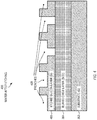
- FIG. 1 shows a side-view cross-section of an example of an integrated circuit 100, in accordance with some embodiments.
- the integrated circuit 100 is shown after assembly but prior to dicing.
- the integrated circuit 100 is but one example of an integrated circuit; other integrated circuits can also be used.
- At least a portion of the integrated circuit 100 can be formed on a silicon-on-insulator wafer, which can include a substrate 102, a buried oxide layer 104 disposed on the substrate 102, and a silicon layer 106 disposed on the buried oxide layer 104.
- the silicon-on-insulator wafer can be ordered from a wafer manufacturer, and provided as an integrated unit as starting material for subsequent processing.
- the buried oxide layer 104 can be grown or deposited on the substrate 102, and the silicon layer 106 can be grown or deposited on the buried oxide layer 104.
- the substrate 102 can play a largely structural role in the device, and can serve as a platform on which other layers or components are deposited, grown, or attached.
- the light propagating in waveguides and other optical elements on the silicon-on-insulator wafer can be confined away from the substrate 102, so that the substrate 102 typically does not play an optical role in a finished device.
- the substrate 102 can be formed from silicon (Si). Silicon is widely used as substrate material because it has relatively high strength, is relatively inexpensive, and is easily processed using typical wafer-level techniques.
- a typical thickness for the silicon substrate 102 is 750 microns, or a value between 725 microns and 775 microns, although other thicknesses can also be used.
- a silicon substrate 102 is typically round, with a diameter of 200 mm, 300 mm, or a value between 200 mm and 300 mm, although other diameters can also be used. Square silicon substrates 102 of appropriate sizes, or other suitable shapes, can also be used.
- a buried oxide layer 104 can be disposed on the substrate 102.
- the buried oxide layer 104 can act as an electrical insulator for components or layers that are positioned above the buried oxide layer 104 (e.g., on the side of the buried oxide layer 104 opposite the substrate 102 ).
- the buried oxide layer 104 can act as cladding material for waveguides that are formed in silicon above the buried oxide layer 104.
- the buried oxide layer 104 can confine most of the light in a waveguide to remain in the waveguide, with a relatively small fraction of the waveguide light leaking into the cladding, and light intensity within the cladding typically following an exponential decay away from the interface between the cladding and the waveguide.
- the buried oxide layer 104 can be formed from silicon dioxide (SiO 2 ).
- silicon dioxide can have a refractive index of about 1.45, which is significantly less than the refractive index of silicon in this wavelength range (about 3.5), and is suitable for use as a cladding material.
- the buried oxide layer 104 can have a thickness of 0.75 microns, 5 microns, a value between 0.75 microns and 5 microns, or another suitable value.
- Other oxide materials can also be used, including sapphire.
- Other wavelength values and ranges can also be used.
- a silicon layer 106 can be disposed on the buried oxide layer 104.
- the silicon layer 106 can be etched to form waveguides and other optical components.
- the silicon layer 106 can be formed from crystalline silicon.
- the silicon layer 106 can be epitaxial, with a specified crystal orientation.
- silicon can be substantially transparent (e.g., with relatively low absorption), with a refractive index of about 3.5.
- the silicon in the silicon layer 106 can be suitable for a core material.
- the silicon layer 106 can have a thickness of 0.5 microns, between 0.3 microns and 0.7 microns, or another suitable value.
- the silicon layer 106 can include one or more waveguides 108 in the silicon layer 106.
- the etched silicon layer 106 can form the waveguide core, with a refractive index of about 3.5 in the wavelength region of 1.0 to 1.5 microns.
- the oxide material 114 above the silicon layer 106 and below the silicon layer 106 (in the buried oxide layer 104 ) can form the waveguide cladding, with a refractive index of about 1.45 in the wavelength region of 1.0 to 1.5 microns.
- the waveguides 108 can be shaped as rib waveguides, which can confine a light beam in two dimensions orthogonal to a direction of propagation in the waveguide. In FIG. 1 , the direction of propagation in the waveguide 108 is orthogonal to the plane of the page.
- the optical waveguides can be rib waveguides that are sized to guide light, the guided light having a frequency corresponding to a first wavelength in air between 1.0 and 1.5 microns.
- the etched walls of the waveguides 108 are kept as close as possible to orthogonal to the plane of the substrate 102. In some examples, the etched walls are angled by between 80 degrees and 90 degrees, with respect to the plane of the substrate 102. In some examples, at least some of the waveguides 108 can have a width of 0.5 microns, 1 micron, 2 microns, a value between 0.3 microns and 3 microns. Other widths can also be used.
- the etched silicon layer 106 can include etched vertical channels 110 extending through the silicon layer 106 to the buried oxide layer 104. These vertical channels 110 can aid with water diffusion, and may not have any appreciable effect on light propagating through the waveguides 108 in the etched silicon layer 106. In some examples, vertical channels 110 can have a width of 1 micron, 10 microns, or a value between 1 micron and 10 microns. Other widths can also be used.
- the etched silicon layer 106 can include etched lateral channels 112 extending only partially into the silicon layer. These lateral channels 112 can also aid with water diffusion, and may not have any appreciable effect on light propagating through the waveguides 108 in the etched silicon layer 106. In some examples, the lateral channels 112 can be etched halfway through the etched silicon layer 106, although other depths can also be used. In some examples, the lateral channels 112 can be etched to the same depth as the waveguides 108. In other examples, the lateral channels 112 can be etched to a different depth than the waveguides 108.
- An oxide material 114 can be disposed on the silicon layer 106.
- the oxide material 114 can extend into the vertical channels 110 and the lateral channels 112 in the silicon layer silicon layer 106.
- the oxide material 114 can be the same material used in the buried oxide layer 104, such as silicon dioxide. Other oxide materials can also be used.
- the oxide material 114 can also fill in volumes above the waveguides 108, so that the oxide material 114 can form a cladding for the silicon core of the waveguides 108.
- the oxide material 114 can be applied during manufacturing, then polished during manufacturing, to form a planarized oxide layer disposed on the silicon layer 106.
- silicon can be used whenever possible, due to its high transparency (e.g., low loss), its ease in processing, and its relatively high mechanical strength. Silicon can be formed into waveguides relatively easily, using typical wafer-level lithographic processes. Silicon is not optically active (e.g., does not produce controllable gain or loss in response to a change in temperature and/or an applied electric field). For instances when optically active material is desired, III-V semiconductor material can be used.
- a III-V semiconductor layer 116 can be disposed on the oxide material 114.
- the III-V semiconductor layer 116 can be formed independently of the substrate 102, buried oxide layer 104, silicon layer 106, and oxide material 114, and placed in contact with the oxide material 114.
- the III-V semiconductor layer 116 can be part of a fully-formed chip that is contacted with the oxide material 114.
- the III-V semiconductor layer 116 can be formed from indium phosphide (InP).
- the III-V semiconductor layer 116 can be formed from one or more of InP, GaAs, GaP, GaN, or InGaAs, or other suitable III-V semiconductor materials.
- water molecules 118 can be forced away from the interface between the III-V semiconductor layer 116 and the oxide material 114, which can enhance bonding between the III-V semiconductor layer 116 and the oxide material 114.
- At least some water molecules 118 present between the III-V semiconductor layer 116 and the oxide material 114 can be forced during manufacturing through the vertical channels 110 into the buried oxide layer 104 thereby to enhance bonding between the III-V semiconductor layer 116 and the oxide material 114.
- the buried oxide layer 104 can have a higher concentration of water molecules 118 than if such forcing were not used. This higher concentration of water molecules 118 may not degrade performance of the buried oxide layer 104, and beneficially can keep the water molecules 118 away from the interface between the III-V semiconductor layer 116 and the oxide material 114.
- At least some water molecules 118 present between the III-V semiconductor layer 116 and the oxide material 114 can be forced during manufacturing into the lateral channels 112, past the periphery of the III-V semiconductor layer 116, and, through diffusion, out of the oxide material 114 into an atmosphere surrounding the periphery of the III-V semiconductor layer 116 and adjacent the oxide material 114.
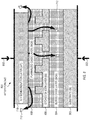
- FIG. 2 shows a top view of selected elements of the integrated circuit 100 of FIG. 1 , in accordance with some embodiments.
- Element 202 is a periphery of the III-V semiconductor layer 116.
- the periphery 202 is rectangular, although other suitable shapes can be used.
- the periphery 202 can be relatively irregular or jagged, corresponding to a specified design of the chip that includes the III-V semiconductor layer 116.
- the vertical channels 110 can extend through the silicon layer 106 to the buried oxide layer 104. In some examples, the vertical channels 110 can be positioned in a first repeating pattern across an area of the III-V semiconductor layer 116. In some examples, each vertical channel 110 can be spaced apart from an adjacent vertical channel 110 by 50 microns, 100 microns, 150 microns, or a value between 50 microns and 150 microns. Other suitable spacings can also be used. The vertical channels 110 can also be spaced irregularly around the area of the III-V semiconductor layer 116, such as to avoid placing a vertical channel 110 on a waveguide 108.
- the lateral channels 112 can extend laterally from an interior of a periphery 202 of the III-V semiconductor layer 116 to an exterior of the periphery of the III-V semiconductor layer 116. In some examples, the lateral channels 112 can be positioned in a second repeating pattern around the periphery 202 of the III-V semiconductor layer 116. In some examples, each lateral channel 112 can be spaced apart from an adjacent lateral channel 112 by between 100 microns and 150 microns, such as to avoid position conflicts between lateral channels 112 and waveguides 108. Other spacings can also be used. The lateral channels 112 can also be spaced irregularly around the periphery 202 of the III-V semiconductor layer 116.
- one or more of the vertical channels 204 can have a circular shape, when viewed from above as in FIG. 2 .
- one or more of the vertical channels 206 can have a square shape, when viewed from above as in FIG. 2 .
- Other shapes can also be used. The shapes can vary from vertical channel 110 to vertical channel 110, as needed.
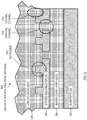
- FIGS. 3-8 show side-view cross-sections of an example of various stages of preparation for the integrated circuit 100 of FIG. 1 .
- FIG. 3 shows an example of a silicon-on-insulator wafer 300, in accordance with some embodiments.
- the structure of FIG. 3 is but one example; other structures can also be used.
- the silicon-on-insulator wafer 300 can include a substrate 302, a buried oxide layer 304 disposed on the substrate 302, and a silicon layer 306 disposed on the buried oxide layer 304.
- the silicon-on-insulator wafer 300 can be ordered from a wafer manufacturer, and provided as an integrated unit as starting material for subsequent processing.
- FIG. 4 shows an example of a silicon-on-insulator wafer 400, after the silicon-on-insulator wafer 400 has been etched, in accordance with some embodiments.
- the structure of FIG. 4 is but one example; other structures can also be used.
- portions of the silicon layer 306 have been etched to form trenches 408 in an etched silicon layer 406.
- the trenches 408 corresponding to the fully etched portions, which extend fully to the buried oxide layer 304, will form the vertical channels when filled downstream with the oxide material.
- the trenches 408 corresponding to the partially etched portions, which extend only partially into the etched silicon layer 406, will form the waveguides and the lateral channels, when filled downstream with the oxide material.
- FIG. 5 shows an example of a silicon-on-insulator wafer 500, after the oxide material has been applied, in accordance with some embodiments.
- the structure of FIG. 5 is but one example; other structures can also be used.
- Oxide material 508 has been applied onto the etched silicon layer 406.
- the applied oxide material 508 can extend into and fill in the etched portions (trenches 408 ) of the etched silicon layer 406.
- the applied oxide material 508 can be the same material used in the buried oxide layer 304.
- the applied oxide material 508 can be silicon dioxide, although other materials can also be used, such as silicon nitride (Si 3 N 4 ), silicon oxynitride (SiO x N y ), or other dielectric films.
- FIG. 6 shows an example of a wafer 600, after the applied oxide material 508 has been polished to form a planarized oxide layer 608, in accordance with some embodiments.
- the structure of FIG. 6 is but one example; other structures can also be used.
- the planarized oxide layer 608 can have a thickness less than a wavelength of light guided by the waveguide 510. In some examples, the planarized oxide layer 608 can have a thickness of 50 nm, 75 nm, 100 nm, or a value between 50 nm and 100 nm. Other suitable thicknesses can also be used. Because the thickness of the planarized oxide layer 608 can be relatively small, compared to the wavelength of the guided light, a significant fraction of the guided light can be present in the planarized oxide layer 608, which can allow relatively efficient coupling between the waveguide 510 and other elements that can be placed in contact with the top of the planarized oxide layer 608.
- FIG. 7 shows an example of a device 700, after a III-V semiconductor layer 710 has been placed in contact with the planarized oxide layer 608, in accordance with some embodiments.
- the III-V semiconductor layer 710 can be in the form of a die, such as a rectangular piece of III-V semiconductor material.
- the III-V semiconductor layer 710 can include a multilayer stack of different III-V semiconductor materials, such as to form a diode with p- and n-doped semiconducting layers, or another suitable structure having a particular electrical function.
- the structure of FIG. 7 is but one example; other structures can also be used.
- the III-V semiconductor layer 710 and the planarized oxide layer 608 may attract water molecules 712 through condensation on the layer surfaces. Such condensation is difficult to avoid, in the absence of a tightly controlled (and thereby expensive) environment. Because the layer surfaces may contain some condensation, placing the III-V semiconductor layer 710 in contact with the planarized oxide layer 608 can trap one or more water molecules 712 at the interface between the III-V semiconductor layer 710 and the planarized oxide layer 608. These trapped water molecules 712 can lead to a failure at the interface, which could involve peel or separating of the planarized oxide layer 608 from the III-V semiconductor layer 710.
- FIG. 8 shows an example of a device 700, after the III-V semiconductor layer 710 has been forced against the planarized oxide layer 608, in accordance with some embodiments.
- the water molecules 712 present at the interface between the III-V semiconductor layer 710 and the planarized oxide layer 608 have been forced into the planarized oxide layer 608 and away from the interface.
- the structure of FIG. 8 is but one example; other structures can also be used.
- the force 802 is shown in FIG. 8 as being applied to compress the substrate 302 against the III-V semiconductor layer 710. It will be understood that this is but one way to impart the force that relocates the trapped water molecules 712; other suitable ways can also be used.
- the substrate 302 can remain stationary, and a force can be applied to the III-V semiconductor layer 710.
- the III-V semiconductor layer 710 can remain stationary, and a force can be applied to the substrate 302.
- both the III-V semiconductor layer 710 and the substrate 302 can be forced against each other.
- the III-V semiconductor layer 710 can be forced against the planarized oxide layer 608 at ambient pressure and at a temperature greater than room temperature. In other examples, the III-V semiconductor layer 710 can be forced against the planarized oxide layer 608 in a vacuum and at a temperature greater than room temperature.
- FIG. 9 shows a flowchart of an example of a method 900 for manufacturing an integrated circuit, in accordance with some embodiments.
- the method 900 is suitable for manufacturing the integrated circuit 100 of FIG. 1 , among other devices.
- the method 900 is but one method for manufacturing an integrated circuit; other suitable methods can also be used.
- the silicon-on-insulator wafer can include a substrate, a buried oxide layer disposed on the substrate, and a silicon layer disposed on the buried oxide layer.
- portions of the silicon layer can be etched to create vertical channels extending through the silicon layer to the buried oxide layer.
- an oxide material can be applied onto the silicon layer.
- the applied oxide material can extend into the vertical channels in the silicon layer.
- the oxide material can be polished to form a planarized oxide layer on the silicon layer.
- a III-V semiconductor layer can be placed in contact with the oxide material, optionally in contact with the planarized oxide layer.
- the III-V semiconductor layer can be placed in contact with the oxide material layer at room temperature.
- the III-V semiconductor layer can be forced against the oxide material (optionally against the planarized oxide layer).
- the water molecules present at an interface between the III-V semiconductor layer and the oxide material can be forced into the oxide layer and away from the interface.
- the water molecules can be forced through the vertical channels into the buried oxide layer thereby to enhance bonding between the III-V semiconductor layer and the oxide material.
- the water molecules can be forced through lateral channels, past a periphery of the III-V semiconductor layer, and, through diffusion, out of the oxide material into an atmosphere surrounding the periphery of the III-V semiconductor layer and adjacent the oxide material.
- one of operations 916 and 918 can be performed but not the other. In other examples, both can be performed.
- the III-V semiconductor layer can be forced against the oxide material at ambient pressure and at a temperature greater than room temperature. In some examples, the III-V semiconductor layer can be forced against the oxide material in a vacuum and at a temperature greater than room temperature.
- the method 900 can optionally further include, prior to applying the oxide material, partially etching portions of the silicon layer to create lateral channels in the silicon layer, the lateral channels positioned such that when the III-V semiconductor layer is placed in contact with the oxide material, the lateral channels extend laterally from an interior of a periphery of the III-V semiconductor layer to an exterior of the periphery of the III-V semiconductor layer.
- the III-V semiconductor layer When the III-V semiconductor layer is forced against the oxide material, at least some of the water molecules present at the interface between the III-V semiconductor layer and the oxide material are forced into the lateral channels, past the periphery of the III-V semiconductor layer, and, through diffusion, out of the oxide material into an atmosphere surrounding the periphery of the III-V semiconductor layer and adjacent the oxide material.
- the vertical channels when the III-V semiconductor layer is placed in contact with the oxide material, can be positioned in a first repeating pattern across an area of the III-V semiconductor layer, and the lateral channels can be positioned in a second repeating pattern around the periphery of the III-V semiconductor layer.
- At least some of the vertical channels can intersect at least some of the lateral channels.
- the method 900 can optionally further include, prior to applying the oxide material, partially etching portions of the silicon layer to create waveguides in the silicon layer.
- the silicon layer can be etched to a first depth to form the lateral channels, and the silicon layer can be etched to a second depth, different from the first depth, to form waveguides in the silicon layer.
- the silicon layer can be etched to a first depth to form the lateral channels and the waveguides in the silicon layer.
- optical elements are formed through mature processes that have been developed for semiconductor manufacturing, such as photolithography and etching.
- photolithography techniques can routinely provide feature sizes down to 45 nm, over a 300 mm-diameter silicon wafer.
- the wafer-level approach offers a significant benefit of scalability. It may be relatively expensive to own or buy time on a photolithography machine, but the expense is easily recovered by the economy of scale.
- a single wafer can produce thousands of parts.
- the parts themselves can include components that are aligned to one another through the lithographic process, which can avoid costly and tedious manual alignment of components to one another.
- the optical system can be packaged as an application-specific integrated circuit (ASIC), and integrated into switching systems alongside other purely electrical ASICs. Along with the convenience in packaging as an ASIC, the optical system can achieve the reliability of an ASIC, with single-chip and solid-state devices that are more reliable than comparable systems formed from discrete components.
- ASIC application-specific integrated circuit
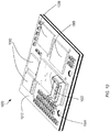
- FIG. 10 shows an example of an optical transceiver 1000, in accordance with some embodiments.
- the optical transceiver 1000 can send and receive optical signals (e.g., optical beams upon which data is encoded).
- the optical transceiver 1000 is suitable for use in data center servers, optical ethernet, and other applications.
- the optical transceiver 1000 can be used for spine-spine servers, spine-leaf servers, and leaf-ToR (top of rack) servers.
- the optical transceiver 1000 can be used in other suitable applications as well.
- the optical transceiver 1000 can include a photonic integrated circuit (PIC) 1002, which can perform any combination of producing light, detecting light, modulating light, demodulating light, amplifying light, attenuating light, separating multi-wavelength light into light at individual wavelengths, combining light at individual wavelengths into multi-wavelength light, and other suitable optical functions.
- PIC photonic integrated circuit
- Waveguides can transport light into and out of the photonic integrated circuit 1002, and can transport light from element to element within the photonic integrated circuit 1002.
- the waveguides can include a core material with a relatively high refractive index, such as silicon, surrounded by a cladding material with a relatively low refractive index, such as silicon dioxide. Both silicon and silicon dioxide are transparent at infrared wavelengths, such as between 1 micron and 1.5 microns.
- the waveguides can be formed in layers on a substrate, such as providing a substrate having a silicon layer on a buried oxide layer, etching trenches in the silicon layer, filling in the trenches with additional oxide material, and polishing the additional oxide material of the filled-in trenches to a desired cladding thickness on a top of the waveguide.
- the waveguides can be shaped as rib waveguides, which can confine a light beam in two dimensions orthogonal to a direction of propagation in the waveguide, and can maintain a constant cross-section along the direction of propagation.
- the rib waveguides can have a trapezoidal cross-section, with parallel top and bottom surfaces (e.g., the surfaces facing toward and away from the substrate on which the waveguides are formed), and angled side surfaces.
- the angle can be 90 degrees, so that the waveguide has a rectangular cross-section. In other examples, the angles can be close to 90 degrees, such as between 80 degrees and 90 degrees, due to limitations in a lithographic exposing or etching process.
- waveguides While some waveguides are intended to transport light from location to location in a photonic integrated circuit, other waveguides can intentionally impart a gain or a loss to the light that passes through the waveguides.
- a waveguide can include an active portion, in which the inactive silicon material can be replaced with an optically active material, such as indium phosphide.
- Some waveguides can be formed with different material than the silicon core and the silicon dioxide cladding.
- one or more of the waveguides can replace some of the silicon core, which is optically inactive, with an active material, such as indium phosphide.
- an active material such as indium phosphide.
- indium phosphide can be used only where optically active material is needed, because it is less transparent, more expensive, and more fragile than silicon.
- the active material can also be placed in the waveguide at the wafer level, using common techniques from the semiconductor industry.
- active material can be used as attenuating material to form an electro-absorption modulator, which can electrically bias the active material to attenuate light at prescribed times.
- the electro-absorption modulator can impart a slowly-varying attenuation onto a light beam, and/or can impart a data signal onto a light beam.
- the inactive waveguides can include reflectors on either side of the active waveguide to form a laser cavity. In some examples, such a laser cavity need not be actively cooled, which can reduce power requirements and simplify the overall design of the photonic integrated circuit.
- output light can be coupled out of the laser cavity through a vertical coupler (e.g., toward or away from the substrate on which the laser is formed).
- a vertical coupler e.g., toward or away from the substrate on which the laser is formed.
- Such vertical coupling can be beneficial in that the laser need not have an active facet from which the laser light emerges. Because active facets can be prone to heat-induced failure, omitting the active facet can help improve the reliability and lifetime of the laser.
- waveguides can be used to form spectral filters, which can transmit light at one or more prescribed wavelengths, and attenuate light away from the prescribed wavelength or wavelengths.
- a Fabry-Perot filter can be formed as a section of a waveguide, the section being bounded by two reflectors in the waveguide.
- the Fabry-Perot filter is transmissive at wavelengths for which the round-trip optical path length between the reflectors equals an integral number of wavelengths, and attenuating for wavelengths away from the transmissive wavelengths.
- a ring resonator can be formed adjacent to a first waveguide.
- a round-trip optical path length around the ring resonator equals an integral number of wavelengths
- light in the first waveguide can couple into the ring resonator, and can couple out of the ring resonator into a second waveguide adjacent to the ring resonator.
- Such a ring resonator exhibits peaked wavelengths, at which there is enhanced coupling into and out of the ring resonator, and minimal coupling away from those peaked wavelengths.
- spectral filters can function in a passive manner, they are typically more useful if they can be actively controlled.
- a portion of the waveguide between the Fabry-Perot reflectors, or within the ring resonator can include an optically active material, which can vary in refractive index as a function of temperature.
- a heater positioned adjacent the optically active material can control a temperature of the active material, can therefore control an optical path length within the spectral filter, and can therefore control the wavelength (or wavelengths) at which the spectral filter is transmissive.
- the active material can be positioned in a separate layer on top of the inactive waveguide.
- Coupling between the waveguides can be achieved by suitably tapering a width of one or both of the waveguides.
- Such a configuration can be convenient for locating a heater adjacent to the active material, so that the heater can be positioned in the same layer as the active material.
- a Mach-Zehnder interferometer can use the heater and variable refractive index material to form an efficient beam attenuator or modulator.
- a Mach-Zehnder interferometer can split an incident beam into two beams, vary an optical path length of one of the beams, then interfere the two beams to produce an output beam.
- the Mach-Zehnder interferometer is transmissive at wavelengths for which the optical path difference between the two arms equals an integral number of wavelengths, and attenuating (to varying degrees) at wavelengths between the transmissive wavelengths. Mach-Zehnder interferometers can function as efficient attenuators or modulators, because the optical path difference required to swing from fully transmissive to fully attenuating is half of a wavelength.
- One or more of a Fabry-Perot cavity, a ring resonator, and/or a Mach-Zehnder interferometer can be combined to form a multiplexer, which can combine two or more input beams at different wavelengths into a single output beam having multiple wavelengths.
- these elements can also be combined to form a demultiplexer, which can separate a single input beam having multiple wavelengths into two or more output beams at different wavelengths.
- the multiplexer and demultiplexer can operate with light having a data signal (e.g., modulated at a particular data rate), or with relatively slowly-varying light that lacks a data signal.
- a photonic integrated circuit 1002 can optionally include one or more photodetectors, which can produce an electrical signal in response to a level of sensed light in a waveguide.
- the electrical signal can be processed by a processor located on the photonic integrated circuit 1002, on the optical transceiver 1000 away from the photonic integrated circuit 1002, or away from the optical transceiver 1000.
- a photonic integrated circuit 1002 can optionally include one or more fiber couplers, which can couple light vertically (e.g., toward or away from the substrate on which the photonic integrated circuit 1002 is formed) into or out of the photonic integrated circuit 1002.
- the fiber coupler can include a relatively precise mechanical housing, such as an optical interface platform 1004, so that the mechanical housing can determine the position and direction of the fiber when the fiber attaches to the housing. Such a precise housing can allow passive coupling to the fiber (as opposed to active coupling, in which a position and/or direction of the fiber is actively adjusted to optimize a coupling efficiency).
- the optical interface platform 1004 can include a rematable fiber interface that can simultaneously attach or detach up to eight fibers, although other values can also be used.
- the photonic integrated circuit 1002 can arrange the optical components described above to form a number of devices.
- the photonic integrated circuit 1002 can be configured as a local area network wavelength division multiplexer (LAN-WDM) or a coarse wavelength division multiplexer (CWDM).
- the photonic integrated circuit 1002 can include a first laser to emit first light at a first wavelength, a first modulator to impart a first data signal onto the first light, a second laser to emit second light at a second wavelength, a second modulator to impart a second data signal onto the second light, a multiplexer to combine the modulated first and second lights into output light, and a first coupler to couple the output light out of the photonic integrated circuit 1002 into an optical fiber.
- the photonic integrated circuit 1002 can include additional lasers and modulators at additional wavelengths, as needed.
- the modulators can be run at faster rates, so that the same platform can be used with successive generations of the photonic integrated circuit 1002.
- channel counts increase over time (e.g., the number of wavelengths present in the output light)
- the number of additional lasers and modulators at additional wavelengths can be increased, as needed.
- the photonic integrated circuit 1002 can be configured to operate in parallel single mode.
- the photonic integrated circuit 1002 can include a first laser to emit first light at a first wavelength, a first modulator to impart a first data signal onto the first light, a first coupler to couple the modulated first light out of the photonic integrated circuit 1002 into a first optical fiber, a second laser to emit second light at a second wavelength, a second modulator to impart a second data signal onto the second light, and a second coupler to couple the modulated second light out of the photonic integrated circuit 1002 into a second optical fiber.
- the photonic integrated circuit 1002 can include additional lasers, modulators, and couplers at additional wavelengths, as needed.
- the optical transceiver 1000 can include a control ASIC 1006, which can control the photonic integrated circuit 1002.
- the control ASIC 1006 can optionally accommodate both electrical and optical signals.
- the optical transceiver 1000 can include a microcontroller 1008, which can control which chips communicate with each other.
- the microcontroller 1008 can include an I-squared-C management interface, which is a synchronous, multi-master, multi-slave, packet switched, single-ended, serial computer bus. Other interfaces can also be used.
- the optical transceiver 1000 can include a chipset 1010, which can correspond to a number of data channels and a data rate.
- the chipset 1010 can have integrated retimers.
- the optical transceiver 1000 can include a substrate 1012, which mechanically supports all the elements of the optical transceiver 1000.
- the substrate 1012 can conform to a standardized size and configuration, such as a 14 mm by 14 mm ball grid array configuration. Other configurations can also be used.
Landscapes
- Optical Integrated Circuits (AREA)
- Recrystallisation Techniques (AREA)
- Internal Circuitry In Semiconductor Integrated Circuit Devices (AREA)
Abstract
Description
- The present disclosure relates generally to bonding of III-V semiconductor material to oxide material during manufacture of integrated circuits, for example, photonic integrated circuits.
- During manufacture of integrated circuits, III-V semiconductor material can be bonded to oxide material. Water molecules can degrade the bonding if they become trapped at the interface between the III-V semiconductor material and the oxide material.
-
-
FIG. 1 shows a side-view cross-section of an example of an integrated circuit, in accordance with some embodiments. -
FIG. 2 shows a top view of selected elements of the integrated circuit ofFIG. 1 , in accordance with some embodiments. -
FIG. 3 shows an example of a silicon-on-insulator wafer, in accordance with some embodiments. -
FIG. 4 shows an example of a silicon-on-insulator wafer, after the silicon-on-insulator wafer has been etched, in accordance with some embodiments. -
FIG. 5 shows an example of a silicon-on-insulator wafer, after the oxide material has been applied, in accordance with some embodiments. -
FIG. 6 shows an example of a wafer, after the applied oxide material has been polished to form a planarized oxide layer, in accordance with some embodiments. -
FIG. 7 shows an example of a device, after a III-V semiconductor layer has been placed in contact with the planarized oxide layer, in accordance with some embodiments. -
FIG. 8 shows an example of a device, after the III-V semiconductor layer has been forced against the planarized oxide layer, in accordance with some embodiments. -
FIG. 9 shows a flowchart of an example of a method for manufacturing an integrated circuit, in accordance with some embodiments. -
FIG. 10 shows an example of an optical transceiver, in accordance with some embodiments. - Corresponding reference characters indicate corresponding parts throughout the several views. Elements in the drawings are not necessarily drawn to scale. The configurations shown in the drawings are merely examples, and should not be construed as limiting the scope of the inventive subject matter in any manner.
- The invention is defined in the appended claims. When III-V semiconductor material is bonded to an oxide material, water molecules can degrade the bonding if they become trapped at the interface between the III-V semiconductor material and the oxide material. Because water molecules can diffuse readily through oxide material, and may not diffuse as readily through III-V semiconductor material or through silicon, forcing the III-V semiconductor material against the oxide material can force water molecules at the interface into the oxide material and away from the interface. The structures discussed below can provide two mechanisms for transporting the water molecules away from the interface, thereby enhancing bonding between the III-V semiconductor material and the oxide material.
- In a first mechanism, the water molecules can be forced through fully-etched portions of a silicon layer, through vertical channels, into a buried oxide layer, which can function like a large reservoir of absorptive material that can absorb water molecules as needed. This first mechanism can transport water molecules along a vertical direction (e.g., in a direction perpendicular to a plane of the silicon layer and the buried oxide layer).
- In a second mechanism, the water molecules can be forced into lateral channels formed in partially-etched portions of the silicon layer. The lateral channels can transport the water molecules past a periphery of the III-V semiconductor material, and, through diffusion, out of the oxide layer into an atmosphere surrounding the periphery of the III-V semiconductor material and adjacent the planarized oxide layer. This second mechanism can transport water molecules along a lateral direction (e.g., within the plane of the silicon layer and the buried oxide layer).
- In some examples, the first mechanism can be used without the second mechanism. In other examples, the second mechanism can be used without the first mechanism. In still other examples, the first and second mechanisms can be used in combination. In some of these examples, some vertical channels can connect with some lateral channels.
- After the water molecules have been forced away from the interface, there can be subsequent wafer-level processing, including dicing into individual components.
-
FIG. 1 shows a side-view cross-section of an example of an integratedcircuit 100, in accordance with some embodiments. The integratedcircuit 100 is shown after assembly but prior to dicing. Theintegrated circuit 100 is but one example of an integrated circuit; other integrated circuits can also be used. - At least a portion of the integrated
circuit 100 can be formed on a silicon-on-insulator wafer, which can include asubstrate 102, a buriedoxide layer 104 disposed on thesubstrate 102, and asilicon layer 106 disposed on the buriedoxide layer 104. In some examples, the silicon-on-insulator wafer can be ordered from a wafer manufacturer, and provided as an integrated unit as starting material for subsequent processing. Alternatively, the buriedoxide layer 104 can be grown or deposited on thesubstrate 102, and thesilicon layer 106 can be grown or deposited on the buriedoxide layer 104. - The
substrate 102 can play a largely structural role in the device, and can serve as a platform on which other layers or components are deposited, grown, or attached. In general, the light propagating in waveguides and other optical elements on the silicon-on-insulator wafer can be confined away from thesubstrate 102, so that thesubstrate 102 typically does not play an optical role in a finished device. - In some examples, the
substrate 102 can be formed from silicon (Si). Silicon is widely used as substrate material because it has relatively high strength, is relatively inexpensive, and is easily processed using typical wafer-level techniques. A typical thickness for thesilicon substrate 102 is 750 microns, or a value between 725 microns and 775 microns, although other thicknesses can also be used. Asilicon substrate 102 is typically round, with a diameter of 200 mm, 300 mm, or a value between 200 mm and 300 mm, although other diameters can also be used.Square silicon substrates 102 of appropriate sizes, or other suitable shapes, can also be used. - A buried
oxide layer 104 can be disposed on thesubstrate 102. The buriedoxide layer 104 can act as an electrical insulator for components or layers that are positioned above the buried oxide layer 104 (e.g., on the side of the buriedoxide layer 104 opposite the substrate 102). - In some examples, the buried
oxide layer 104 can act as cladding material for waveguides that are formed in silicon above the buriedoxide layer 104. When used as a cladding, the buriedoxide layer 104 can confine most of the light in a waveguide to remain in the waveguide, with a relatively small fraction of the waveguide light leaking into the cladding, and light intensity within the cladding typically following an exponential decay away from the interface between the cladding and the waveguide. - In some examples, the buried
oxide layer 104 can be formed from silicon dioxide (SiO2). In a wavelength range of 1.0 to 1.5 microns, silicon dioxide can have a refractive index of about 1.45, which is significantly less than the refractive index of silicon in this wavelength range (about 3.5), and is suitable for use as a cladding material. In some examples, the buriedoxide layer 104 can have a thickness of 0.75 microns, 5 microns, a value between 0.75 microns and 5 microns, or another suitable value. Other oxide materials can also be used, including sapphire. Other wavelength values and ranges can also be used. - A
silicon layer 106 can be disposed on the buriedoxide layer 104. Thesilicon layer 106 can be etched to form waveguides and other optical components. In some examples, thesilicon layer 106 can be formed from crystalline silicon. In some examples, thesilicon layer 106 can be epitaxial, with a specified crystal orientation. - In a wavelength range of 1.0 to 1.5 microns, silicon can be substantially transparent (e.g., with relatively low absorption), with a refractive index of about 3.5. When etched into a suitably shaped waveguide, the silicon in the
silicon layer 106 can be suitable for a core material. In some examples, thesilicon layer 106 can have a thickness of 0.5 microns, between 0.3 microns and 0.7 microns, or another suitable value. - The
silicon layer 106 can include one ormore waveguides 108 in thesilicon layer 106. Theetched silicon layer 106 can form the waveguide core, with a refractive index of about 3.5 in the wavelength region of 1.0 to 1.5 microns. Theoxide material 114 above thesilicon layer 106 and below the silicon layer 106 (in the buried oxide layer 104) can form the waveguide cladding, with a refractive index of about 1.45 in the wavelength region of 1.0 to 1.5 microns. - In some examples, the
waveguides 108 can be shaped as rib waveguides, which can confine a light beam in two dimensions orthogonal to a direction of propagation in the waveguide. InFIG. 1 , the direction of propagation in thewaveguide 108 is orthogonal to the plane of the page. In some examples, the optical waveguides can be rib waveguides that are sized to guide light, the guided light having a frequency corresponding to a first wavelength in air between 1.0 and 1.5 microns. - In some examples, the etched walls of the
waveguides 108 are kept as close as possible to orthogonal to the plane of thesubstrate 102. In some examples, the etched walls are angled by between 80 degrees and 90 degrees, with respect to the plane of thesubstrate 102. In some examples, at least some of thewaveguides 108 can have a width of 0.5 microns, 1 micron, 2 microns, a value between 0.3 microns and 3 microns. Other widths can also be used. - The etched
silicon layer 106 can include etchedvertical channels 110 extending through thesilicon layer 106 to the buriedoxide layer 104. Thesevertical channels 110 can aid with water diffusion, and may not have any appreciable effect on light propagating through thewaveguides 108 in the etchedsilicon layer 106. In some examples,vertical channels 110 can have a width of 1 micron, 10 microns, or a value between 1 micron and 10 microns. Other widths can also be used. - In addition to, or instead of the
vertical channels 110, the etchedsilicon layer 106 can include etchedlateral channels 112 extending only partially into the silicon layer. Theselateral channels 112 can also aid with water diffusion, and may not have any appreciable effect on light propagating through thewaveguides 108 in the etchedsilicon layer 106. In some examples, thelateral channels 112 can be etched halfway through the etchedsilicon layer 106, although other depths can also be used. In some examples, thelateral channels 112 can be etched to the same depth as thewaveguides 108. In other examples, thelateral channels 112 can be etched to a different depth than thewaveguides 108. - An
oxide material 114 can be disposed on thesilicon layer 106. Theoxide material 114 can extend into thevertical channels 110 and thelateral channels 112 in the siliconlayer silicon layer 106. In some examples, theoxide material 114 can be the same material used in the buriedoxide layer 104, such as silicon dioxide. Other oxide materials can also be used. Theoxide material 114 can also fill in volumes above thewaveguides 108, so that theoxide material 114 can form a cladding for the silicon core of thewaveguides 108. In some examples, theoxide material 114 can be applied during manufacturing, then polished during manufacturing, to form a planarized oxide layer disposed on thesilicon layer 106. - In most photonic integrated circuits, silicon can be used whenever possible, due to its high transparency (e.g., low loss), its ease in processing, and its relatively high mechanical strength. Silicon can be formed into waveguides relatively easily, using typical wafer-level lithographic processes. Silicon is not optically active (e.g., does not produce controllable gain or loss in response to a change in temperature and/or an applied electric field). For instances when optically active material is desired, III-V semiconductor material can be used.
- A III-
V semiconductor layer 116 can be disposed on theoxide material 114. In some examples, the III-V semiconductor layer 116 can be formed independently of thesubstrate 102, buriedoxide layer 104,silicon layer 106, andoxide material 114, and placed in contact with theoxide material 114. In some examples, the III-V semiconductor layer 116 can be part of a fully-formed chip that is contacted with theoxide material 114. In some examples, the III-V semiconductor layer 116 can be formed from indium phosphide (InP). In other examples, the III-V semiconductor layer 116 can be formed from one or more of InP, GaAs, GaP, GaN, or InGaAs, or other suitable III-V semiconductor materials. - During manufacturing,
water molecules 118 can be forced away from the interface between the III-V semiconductor layer 116 and theoxide material 114, which can enhance bonding between the III-V semiconductor layer 116 and theoxide material 114. - In some examples, at least some
water molecules 118 present between the III-V semiconductor layer 116 and theoxide material 114 can be forced during manufacturing through thevertical channels 110 into the buriedoxide layer 104 thereby to enhance bonding between the III-V semiconductor layer 116 and theoxide material 114. In some examples, due to this forcing during manufacturing, the buriedoxide layer 104 can have a higher concentration ofwater molecules 118 than if such forcing were not used. This higher concentration ofwater molecules 118 may not degrade performance of the buriedoxide layer 104, and beneficially can keep thewater molecules 118 away from the interface between the III-V semiconductor layer 116 and theoxide material 114. - In some examples, at least some
water molecules 118 present between the III-V semiconductor layer 116 and theoxide material 114 can be forced during manufacturing into thelateral channels 112, past the periphery of the III-V semiconductor layer 116, and, through diffusion, out of theoxide material 114 into an atmosphere surrounding the periphery of the III-V semiconductor layer 116 and adjacent theoxide material 114. -
FIG. 2 shows a top view of selected elements of theintegrated circuit 100 ofFIG. 1 , in accordance with some embodiments. -
Element 202 is a periphery of the III-V semiconductor layer 116. In the example ofFIG. 2 , theperiphery 202 is rectangular, although other suitable shapes can be used. In some examples, theperiphery 202 can be relatively irregular or jagged, corresponding to a specified design of the chip that includes the III-V semiconductor layer 116. - In some examples, the
vertical channels 110 can extend through thesilicon layer 106 to the buriedoxide layer 104. In some examples, thevertical channels 110 can be positioned in a first repeating pattern across an area of the III-V semiconductor layer 116. In some examples, eachvertical channel 110 can be spaced apart from an adjacentvertical channel 110 by 50 microns, 100 microns, 150 microns, or a value between 50 microns and 150 microns. Other suitable spacings can also be used. Thevertical channels 110 can also be spaced irregularly around the area of the III-V semiconductor layer 116, such as to avoid placing avertical channel 110 on awaveguide 108. - In some examples, the
lateral channels 112 can extend laterally from an interior of aperiphery 202 of the III-V semiconductor layer 116 to an exterior of the periphery of the III-V semiconductor layer 116. In some examples, thelateral channels 112 can be positioned in a second repeating pattern around theperiphery 202 of the III-V semiconductor layer 116. In some examples, eachlateral channel 112 can be spaced apart from an adjacentlateral channel 112 by between 100 microns and 150 microns, such as to avoid position conflicts betweenlateral channels 112 andwaveguides 108. Other spacings can also be used. Thelateral channels 112 can also be spaced irregularly around theperiphery 202 of the III-V semiconductor layer 116. - In some examples, one or more of the
vertical channels 204 can have a circular shape, when viewed from above as inFIG. 2 . In some examples, one or more of thevertical channels 206 can have a square shape, when viewed from above as inFIG. 2 . Other shapes can also be used. The shapes can vary fromvertical channel 110 tovertical channel 110, as needed. -
FIGS. 3-8 show side-view cross-sections of an example of various stages of preparation for theintegrated circuit 100 ofFIG. 1 . -
FIG. 3 shows an example of a silicon-on-insulator wafer 300, in accordance with some embodiments. The structure ofFIG. 3 is but one example; other structures can also be used. - The silicon-on-
insulator wafer 300 can include asubstrate 302, a buriedoxide layer 304 disposed on thesubstrate 302, and asilicon layer 306 disposed on the buriedoxide layer 304. In this example, the silicon-on-insulator wafer 300 can be ordered from a wafer manufacturer, and provided as an integrated unit as starting material for subsequent processing. -
FIG. 4 shows an example of a silicon-on-insulator wafer 400, after the silicon-on-insulator wafer 400 has been etched, in accordance with some embodiments. The structure ofFIG. 4 is but one example; other structures can also be used. - In some examples, portions of the
silicon layer 306 have been etched to formtrenches 408 in an etchedsilicon layer 406. Thetrenches 408 corresponding to the fully etched portions, which extend fully to the buriedoxide layer 304, will form the vertical channels when filled downstream with the oxide material. Thetrenches 408 corresponding to the partially etched portions, which extend only partially into the etchedsilicon layer 406, will form the waveguides and the lateral channels, when filled downstream with the oxide material. -
FIG. 5 shows an example of a silicon-on-insulator wafer 500, after the oxide material has been applied, in accordance with some embodiments. The structure ofFIG. 5 is but one example; other structures can also be used. -
Oxide material 508 has been applied onto the etchedsilicon layer 406. The appliedoxide material 508 can extend into and fill in the etched portions (trenches 408) of the etchedsilicon layer 406. In some examples, the appliedoxide material 508 can be the same material used in the buriedoxide layer 304. In some examples, the appliedoxide material 508 can be silicon dioxide, although other materials can also be used, such as silicon nitride (Si3N4), silicon oxynitride (SiOxNy), or other dielectric films.Element 510 is a waveguide, having a silicon core formed from the etchedsilicon layer 406, and a silicon dioxide cladding, formed from the buriedoxide layer 304 below thewaveguide 510 and the appliedoxide material 508 above thewaveguide 510.Element 512 is a vertical channel.Element 514 is a lateral channel. -
FIG. 6 shows an example of awafer 600, after the appliedoxide material 508 has been polished to form aplanarized oxide layer 608, in accordance with some embodiments. The structure ofFIG. 6 is but one example; other structures can also be used. - In some examples, the
planarized oxide layer 608 can have a thickness less than a wavelength of light guided by thewaveguide 510. In some examples, theplanarized oxide layer 608 can have a thickness of 50 nm, 75 nm, 100 nm, or a value between 50 nm and 100 nm. Other suitable thicknesses can also be used. Because the thickness of theplanarized oxide layer 608 can be relatively small, compared to the wavelength of the guided light, a significant fraction of the guided light can be present in theplanarized oxide layer 608, which can allow relatively efficient coupling between thewaveguide 510 and other elements that can be placed in contact with the top of theplanarized oxide layer 608. -
FIG. 7 shows an example of adevice 700, after a III-V semiconductor layer 710 has been placed in contact with theplanarized oxide layer 608, in accordance with some embodiments. In some examples, the III-V semiconductor layer 710 can be in the form of a die, such as a rectangular piece of III-V semiconductor material. In some examples, the III-V semiconductor layer 710 can include a multilayer stack of different III-V semiconductor materials, such as to form a diode with p- and n-doped semiconducting layers, or another suitable structure having a particular electrical function. The structure ofFIG. 7 is but one example; other structures can also be used. - In practice, the III-
V semiconductor layer 710 and theplanarized oxide layer 608 may attractwater molecules 712 through condensation on the layer surfaces. Such condensation is difficult to avoid, in the absence of a tightly controlled (and thereby expensive) environment. Because the layer surfaces may contain some condensation, placing the III-V semiconductor layer 710 in contact with theplanarized oxide layer 608 can trap one ormore water molecules 712 at the interface between the III-V semiconductor layer 710 and theplanarized oxide layer 608. These trappedwater molecules 712 can lead to a failure at the interface, which could involve peel or separating of theplanarized oxide layer 608 from the III-V semiconductor layer 710. - Because water molecules can diffuse readily through oxide material, forcing the III-
V semiconductor layer 710 against theplanarized oxide layer 608 can force thewater molecules 712 at the interface into theplanarized oxide layer 608 and away from the interface. -
FIG. 8 shows an example of adevice 700, after the III-V semiconductor layer 710 has been forced against theplanarized oxide layer 608, in accordance with some embodiments. Thewater molecules 712 present at the interface between the III-V semiconductor layer 710 and theplanarized oxide layer 608 have been forced into theplanarized oxide layer 608 and away from the interface. The structure ofFIG. 8 is but one example; other structures can also be used. - The
force 802 is shown inFIG. 8 as being applied to compress thesubstrate 302 against the III-V semiconductor layer 710. It will be understood that this is but one way to impart the force that relocates the trappedwater molecules 712; other suitable ways can also be used. For example, thesubstrate 302 can remain stationary, and a force can be applied to the III-V semiconductor layer 710. Alternatively, the III-V semiconductor layer 710 can remain stationary, and a force can be applied to thesubstrate 302. As a further alternative, both the III-V semiconductor layer 710 and thesubstrate 302 can be forced against each other. - In some examples, the III-
V semiconductor layer 710 can be forced against theplanarized oxide layer 608 at ambient pressure and at a temperature greater than room temperature. In other examples, the III-V semiconductor layer 710 can be forced against theplanarized oxide layer 608 in a vacuum and at a temperature greater than room temperature. - After the water molecules have been forced away from the interface, there can be subsequent wafer-level processing of the III-
V semiconductor layer 710 and/or the silicon-on-insulator wafer, including dicing into individual components. -
FIG. 9 shows a flowchart of an example of amethod 900 for manufacturing an integrated circuit, in accordance with some embodiments. Themethod 900 is suitable for manufacturing theintegrated circuit 100 ofFIG. 1 , among other devices. Themethod 900 is but one method for manufacturing an integrated circuit; other suitable methods can also be used. - At
operation 902, a silicon-on-insulator wafer is provided. The silicon-on-insulator wafer can include a substrate, a buried oxide layer disposed on the substrate, and a silicon layer disposed on the buried oxide layer. - At
operation 904, portions of the silicon layer can be etched to create vertical channels extending through the silicon layer to the buried oxide layer. - At
operation 906, an oxide material can be applied onto the silicon layer. The applied oxide material can extend into the vertical channels in the silicon layer. - At
optional operation 908, the oxide material can be polished to form a planarized oxide layer on the silicon layer. - At
operation 910, a III-V semiconductor layer can be placed in contact with the oxide material, optionally in contact with the planarized oxide layer. In some examples, the III-V semiconductor layer can be placed in contact with the oxide material layer at room temperature. - At
operation 912, the III-V semiconductor layer can be forced against the oxide material (optionally against the planarized oxide layer). - At
operation 914, the water molecules present at an interface between the III-V semiconductor layer and the oxide material can be forced into the oxide layer and away from the interface. - At
operation 916, the water molecules can be forced through the vertical channels into the buried oxide layer thereby to enhance bonding between the III-V semiconductor layer and the oxide material. - At
operation 918, the water molecules can be forced through lateral channels, past a periphery of the III-V semiconductor layer, and, through diffusion, out of the oxide material into an atmosphere surrounding the periphery of the III-V semiconductor layer and adjacent the oxide material. - In some examples, one of
operations - In some examples, the III-V semiconductor layer can be forced against the oxide material at ambient pressure and at a temperature greater than room temperature. In some examples, the III-V semiconductor layer can be forced against the oxide material in a vacuum and at a temperature greater than room temperature.
- In some examples, the
method 900 can optionally further include, prior to applying the oxide material, partially etching portions of the silicon layer to create lateral channels in the silicon layer, the lateral channels positioned such that when the III-V semiconductor layer is placed in contact with the oxide material, the lateral channels extend laterally from an interior of a periphery of the III-V semiconductor layer to an exterior of the periphery of the III-V semiconductor layer. When the III-V semiconductor layer is forced against the oxide material, at least some of the water molecules present at the interface between the III-V semiconductor layer and the oxide material are forced into the lateral channels, past the periphery of the III-V semiconductor layer, and, through diffusion, out of the oxide material into an atmosphere surrounding the periphery of the III-V semiconductor layer and adjacent the oxide material. - In some examples, when the III-V semiconductor layer is placed in contact with the oxide material, the vertical channels can be positioned in a first repeating pattern across an area of the III-V semiconductor layer, and the lateral channels can be positioned in a second repeating pattern around the periphery of the III-V semiconductor layer.
- In some examples, at least some of the vertical channels can intersect at least some of the lateral channels.
- In some examples, the
method 900 can optionally further include, prior to applying the oxide material, partially etching portions of the silicon layer to create waveguides in the silicon layer. - In some examples, the silicon layer can be etched to a first depth to form the lateral channels, and the silicon layer can be etched to a second depth, different from the first depth, to form waveguides in the silicon layer.
- In some examples, the silicon layer can be etched to a first depth to form the lateral channels and the waveguides in the silicon layer.
- After the water molecules have been forced away from the interface, there can be subsequent wafer-level processing of the III-V semiconductor chip and/or the silicon-on-insulator wafer, including dicing into individual components.
- The devices, systems, and methods discussed above rely on wafer-level processes for manufacturing and alignment. Most or all optical elements are formed through mature processes that have been developed for semiconductor manufacturing, such as photolithography and etching. For example, current photolithography techniques can routinely provide feature sizes down to 45 nm, over a 300 mm-diameter silicon wafer.
- Compared to more traditional optical systems, in which components are manufactured discretely and aligned to one another, the wafer-level approach offers a significant benefit of scalability. It may be relatively expensive to own or buy time on a photolithography machine, but the expense is easily recovered by the economy of scale. A single wafer can produce thousands of parts. In addition, the parts themselves can include components that are aligned to one another through the lithographic process, which can avoid costly and tedious manual alignment of components to one another. In addition, the optical system can be packaged as an application-specific integrated circuit (ASIC), and integrated into switching systems alongside other purely electrical ASICs. Along with the convenience in packaging as an ASIC, the optical system can achieve the reliability of an ASIC, with single-chip and solid-state devices that are more reliable than comparable systems formed from discrete components.
-
FIG. 10 shows an example of anoptical transceiver 1000, in accordance with some embodiments. Theoptical transceiver 1000 can send and receive optical signals (e.g., optical beams upon which data is encoded). Theoptical transceiver 1000 is suitable for use in data center servers, optical ethernet, and other applications. For example, in a cloud data center network, theoptical transceiver 1000 can be used for spine-spine servers, spine-leaf servers, and leaf-ToR (top of rack) servers. Theoptical transceiver 1000 can be used in other suitable applications as well. - The
optical transceiver 1000 can include a photonic integrated circuit (PIC) 1002, which can perform any combination of producing light, detecting light, modulating light, demodulating light, amplifying light, attenuating light, separating multi-wavelength light into light at individual wavelengths, combining light at individual wavelengths into multi-wavelength light, and other suitable optical functions. - Waveguides can transport light into and out of the photonic
integrated circuit 1002, and can transport light from element to element within the photonicintegrated circuit 1002. The waveguides can include a core material with a relatively high refractive index, such as silicon, surrounded by a cladding material with a relatively low refractive index, such as silicon dioxide. Both silicon and silicon dioxide are transparent at infrared wavelengths, such as between 1 micron and 1.5 microns. In some examples, the waveguides can be formed in layers on a substrate, such as providing a substrate having a silicon layer on a buried oxide layer, etching trenches in the silicon layer, filling in the trenches with additional oxide material, and polishing the additional oxide material of the filled-in trenches to a desired cladding thickness on a top of the waveguide. In some examples, the waveguides can be shaped as rib waveguides, which can confine a light beam in two dimensions orthogonal to a direction of propagation in the waveguide, and can maintain a constant cross-section along the direction of propagation. In some examples, the rib waveguides can have a trapezoidal cross-section, with parallel top and bottom surfaces (e.g., the surfaces facing toward and away from the substrate on which the waveguides are formed), and angled side surfaces. In some examples, the angle can be 90 degrees, so that the waveguide has a rectangular cross-section. In other examples, the angles can be close to 90 degrees, such as between 80 degrees and 90 degrees, due to limitations in a lithographic exposing or etching process. - While some waveguides are intended to transport light from location to location in a photonic integrated circuit, other waveguides can intentionally impart a gain or a loss to the light that passes through the waveguides. For example, a waveguide can include an active portion, in which the inactive silicon material can be replaced with an optically active material, such as indium phosphide.
- Some waveguides can be formed with different material than the silicon core and the silicon dioxide cladding. For example, one or more of the waveguides can replace some of the silicon core, which is optically inactive, with an active material, such as indium phosphide. By electrically biasing the active material, light passing through the active material can be selectively amplified or absorbed. In general, indium phosphide can be used only where optically active material is needed, because it is less transparent, more expensive, and more fragile than silicon. The active material can also be placed in the waveguide at the wafer level, using common techniques from the semiconductor industry.
- In some examples, it may be desirable to couple light from one waveguide to another waveguide. For example, it may be desirable to couple light from an inactive waveguide to a separate active waveguide that includes an active portion, then back to the inactive waveguide. For these cases, it may be convenient to position the active waveguide in a separate layer on top of the inactive waveguide. Coupling between the waveguides can be achieved by suitably tapering a width of one or both of the waveguides. Such a configuration can be convenient for locating electrodes on opposite sides of the active portion, so that the electrodes can be positioned in the same layer as the active material.
- In some examples, active material can be used as attenuating material to form an electro-absorption modulator, which can electrically bias the active material to attenuate light at prescribed times. The electro-absorption modulator can impart a slowly-varying attenuation onto a light beam, and/or can impart a data signal onto a light beam. Alternatively, when the active material is used to impart gain onto light in the active waveguide, the inactive waveguides can include reflectors on either side of the active waveguide to form a laser cavity. In some examples, such a laser cavity need not be actively cooled, which can reduce power requirements and simplify the overall design of the photonic integrated circuit. In some examples, output light can be coupled out of the laser cavity through a vertical coupler (e.g., toward or away from the substrate on which the laser is formed). Such vertical coupling can be beneficial in that the laser need not have an active facet from which the laser light emerges. Because active facets can be prone to heat-induced failure, omitting the active facet can help improve the reliability and lifetime of the laser.
- In some examples, waveguides can be used to form spectral filters, which can transmit light at one or more prescribed wavelengths, and attenuate light away from the prescribed wavelength or wavelengths. For example, a Fabry-Perot filter can be formed as a section of a waveguide, the section being bounded by two reflectors in the waveguide. The Fabry-Perot filter is transmissive at wavelengths for which the round-trip optical path length between the reflectors equals an integral number of wavelengths, and attenuating for wavelengths away from the transmissive wavelengths. As another example, a ring resonator can be formed adjacent to a first waveguide. When a round-trip optical path length around the ring resonator equals an integral number of wavelengths, light in the first waveguide can couple into the ring resonator, and can couple out of the ring resonator into a second waveguide adjacent to the ring resonator. Such a ring resonator exhibits peaked wavelengths, at which there is enhanced coupling into and out of the ring resonator, and minimal coupling away from those peaked wavelengths.
- Although these spectral filters can function in a passive manner, they are typically more useful if they can be actively controlled. For example, a portion of the waveguide between the Fabry-Perot reflectors, or within the ring resonator, can include an optically active material, which can vary in refractive index as a function of temperature. A heater positioned adjacent the optically active material can control a temperature of the active material, can therefore control an optical path length within the spectral filter, and can therefore control the wavelength (or wavelengths) at which the spectral filter is transmissive. In some examples, the active material can be positioned in a separate layer on top of the inactive waveguide. Coupling between the waveguides can be achieved by suitably tapering a width of one or both of the waveguides. Such a configuration can be convenient for locating a heater adjacent to the active material, so that the heater can be positioned in the same layer as the active material.
- A Mach-Zehnder interferometer can use the heater and variable refractive index material to form an efficient beam attenuator or modulator. A Mach-Zehnder interferometer can split an incident beam into two beams, vary an optical path length of one of the beams, then interfere the two beams to produce an output beam. The Mach-Zehnder interferometer is transmissive at wavelengths for which the optical path difference between the two arms equals an integral number of wavelengths, and attenuating (to varying degrees) at wavelengths between the transmissive wavelengths. Mach-Zehnder interferometers can function as efficient attenuators or modulators, because the optical path difference required to swing from fully transmissive to fully attenuating is half of a wavelength.
- One or more of a Fabry-Perot cavity, a ring resonator, and/or a Mach-Zehnder interferometer can be combined to form a multiplexer, which can combine two or more input beams at different wavelengths into a single output beam having multiple wavelengths. Similarly, these elements can also be combined to form a demultiplexer, which can separate a single input beam having multiple wavelengths into two or more output beams at different wavelengths. The multiplexer and demultiplexer can operate with light having a data signal (e.g., modulated at a particular data rate), or with relatively slowly-varying light that lacks a data signal.
- A photonic
integrated circuit 1002 can optionally include one or more photodetectors, which can produce an electrical signal in response to a level of sensed light in a waveguide. The electrical signal can be processed by a processor located on the photonicintegrated circuit 1002, on theoptical transceiver 1000 away from the photonicintegrated circuit 1002, or away from theoptical transceiver 1000. - A photonic
integrated circuit 1002 can optionally include one or more fiber couplers, which can couple light vertically (e.g., toward or away from the substrate on which the photonicintegrated circuit 1002 is formed) into or out of the photonicintegrated circuit 1002. In some examples, the fiber coupler can include a relatively precise mechanical housing, such as anoptical interface platform 1004, so that the mechanical housing can determine the position and direction of the fiber when the fiber attaches to the housing. Such a precise housing can allow passive coupling to the fiber (as opposed to active coupling, in which a position and/or direction of the fiber is actively adjusted to optimize a coupling efficiency). In some examples, theoptical interface platform 1004 can include a rematable fiber interface that can simultaneously attach or detach up to eight fibers, although other values can also be used. - The photonic
integrated circuit 1002 can arrange the optical components described above to form a number of devices. - For example, the photonic
integrated circuit 1002 can be configured as a local area network wavelength division multiplexer (LAN-WDM) or a coarse wavelength division multiplexer (CWDM). The photonicintegrated circuit 1002 can include a first laser to emit first light at a first wavelength, a first modulator to impart a first data signal onto the first light, a second laser to emit second light at a second wavelength, a second modulator to impart a second data signal onto the second light, a multiplexer to combine the modulated first and second lights into output light, and a first coupler to couple the output light out of the photonicintegrated circuit 1002 into an optical fiber. The photonicintegrated circuit 1002 can include additional lasers and modulators at additional wavelengths, as needed. As standardized data rates increase over time, the modulators can be run at faster rates, so that the same platform can be used with successive generations of the photonicintegrated circuit 1002. Similarly, as channel counts increase over time (e.g., the number of wavelengths present in the output light), the number of additional lasers and modulators at additional wavelengths can be increased, as needed. - As another example, the photonic
integrated circuit 1002 can be configured to operate in parallel single mode. The photonicintegrated circuit 1002 can include a first laser to emit first light at a first wavelength, a first modulator to impart a first data signal onto the first light, a first coupler to couple the modulated first light out of the photonicintegrated circuit 1002 into a first optical fiber, a second laser to emit second light at a second wavelength, a second modulator to impart a second data signal onto the second light, and a second coupler to couple the modulated second light out of the photonicintegrated circuit 1002 into a second optical fiber. The photonicintegrated circuit 1002 can include additional lasers, modulators, and couplers at additional wavelengths, as needed. - The
optical transceiver 1000 can include acontrol ASIC 1006, which can control the photonicintegrated circuit 1002. Thecontrol ASIC 1006 can optionally accommodate both electrical and optical signals. - The
optical transceiver 1000 can include amicrocontroller 1008, which can control which chips communicate with each other. In some examples, themicrocontroller 1008 can include an I-squared-C management interface, which is a synchronous, multi-master, multi-slave, packet switched, single-ended, serial computer bus. Other interfaces can also be used. - The
optical transceiver 1000 can include achipset 1010, which can correspond to a number of data channels and a data rate. In some examples, thechipset 1010 can have integrated retimers. - The
optical transceiver 1000 can include asubstrate 1012, which mechanically supports all the elements of theoptical transceiver 1000. In some examples, thesubstrate 1012 can conform to a standardized size and configuration, such as a 14 mm by 14 mm ball grid array configuration. Other configurations can also be used. - In the foregoing detailed description, the method and apparatus of the present disclosure have been described with reference to specific embodiments thereof. It will, however, be evident that various modifications and changes may be made thereto without departing from the scope of the claims. The present description and figures are accordingly to be regarded as illustrative rather than restrictive.
- To further illustrate the device and related method disclosed herein, a non-limiting list of examples is provided below. Each of the following non-limiting examples can stand on its own, or can be combined in any permutation or combination with any one or more of the other examples.
- In Example 1, an integrated circuit can include: a substrate; a buried oxide layer disposed on the substrate; a silicon layer disposed on the buried oxide layer, the silicon layer including etched vertical channels extending through the silicon layer to the buried oxide layer; an oxide material disposed on the silicon layer, the oxide material extending into the vertical channels in the silicon layer; and a III-V semiconductor layer disposed on the oxide material, wherein water molecules present between the III-V semiconductor layer and the oxide material are forced during manufacturing through the vertical channels into the buried oxide layer thereby to enhance bonding between the III-V semiconductor layer and the oxide material.
- In Example 2, the integrated circuit of Example 1 can optionally be configured such that the silicon layer further includes etched lateral channels extending only partially into the silicon layer, the oxide material extending into the lateral channels in the silicon layer, the lateral channels extending laterally from an interior of a periphery of the III-V semiconductor layer to an exterior of the periphery of the III-V semiconductor layer.
- In Example 3, the integrated circuit of any one of Examples 1-2 can optionally be configured such that the vertical channels are positioned in a first repeating pattern across an area of the III-V semiconductor layer; and the lateral channels are positioned in a second repeating pattern around the periphery of the III-V semiconductor layer.
- In Example 4, the integrated circuit of any one of Examples 1-3 can optionally be configured such that at least some of the vertical channels intersect at least some of the lateral channels.
- In Example 5, the integrated circuit of any one of Examples 1-4 can optionally be configured such that the oxide material is applied during manufacturing, then polished during manufacturing, to form a planarized oxide layer disposed on the silicon layer.
- In Example 6, the integrated circuit of any one of Examples 1-5 can optionally be configured such that the III-V semiconductor layer is included on a III-V semiconductor chip; and during manufacturing, the III-V semiconductor chip is forced against the planarized oxide layer to force the water molecules through the vertical channels into the buried oxide layer.
- In Example 7, the integrated circuit of any one of Examples 1-6 can optionally be configured such that during manufacturing: the silicon layer is etched to a first depth to form the lateral channels; and the silicon layer is etched to a second depth, different from the first depth, to form waveguides in the silicon layer.
- In Example 8, the integrated circuit of any one of Examples 1-7 can optionally be configured such that during manufacturing: the silicon layer is etched to a first depth to form the lateral channels and to form waveguides in the silicon layer.
- In Example 9, the integrated circuit of any one of Examples 1-8 can optionally be configured such that the substrate is formed from silicon (Si); the buried oxide layer is formed from silicon dioxide (SiO2); the oxide material is silicon dioxide; and the III-V semiconductor layer is formed from indium phosphide (InP).
- In Example 10, a method of manufacturing an integrated circuit can include: providing a silicon-on-insulator wafer including a substrate, a buried oxide layer disposed on the substrate, and a silicon layer disposed on the buried oxide layer; etching portions of the silicon layer to create vertical channels extending through the silicon layer to the buried oxide layer; applying an oxide material onto the silicon layer, the applied oxide material extending into the vertical channels in the silicon layer; placing a III-V semiconductor layer in contact with the oxide material; and forcing the III-V semiconductor layer against the oxide material to force water molecules present at an interface between the III-V semiconductor layer and the oxide material through the vertical channels into the buried oxide layer thereby to enhance bonding between the III-V semiconductor layer and the oxide material.
- In Example 11, the method of Example 10 can optionally further include, prior to applying the oxide material: partially etching portions of the silicon layer to create lateral channels in the silicon layer, the lateral channels positioned such that when the III-V semiconductor layer is placed in contact with the oxide material, the lateral channels extend laterally from an interior of a periphery of the III-V semiconductor layer to an exterior of the periphery of the III-V semiconductor layer, wherein when the III-V semiconductor layer is forced against the oxide material, at least some of the water molecules present at the interface between the III-V semiconductor layer and the oxide material are forced into the lateral channels, past the periphery of the III-V semiconductor layer, and, through diffusion, out of the oxide material into an atmosphere surrounding the periphery of the III-V semiconductor layer and adjacent the oxide material.
- In Example 12, the method of any one of Examples 10-11 can optionally be configured such that when the III-V semiconductor layer is placed in contact with the oxide material: the vertical channels are positioned in a first repeating pattern across an area of the III-V semiconductor layer; and the lateral channels are positioned in a second repeating pattern around the periphery of the III-V semiconductor layer.
- In Example 13, the method of any one of Examples 10-12 can optionally be configured such that at least some of the vertical channels intersect at least some of the lateral channels.
- In Example 14, the method of any one of Examples 10-13 can optionally further include, prior to applying the oxide material: partially etching portions of the silicon layer to create waveguides in the silicon layer.
- In Example 15, the method of any one of Examples 10-14 can optionally be configured such that the silicon layer is etched to a first depth to form the lateral channels; and the silicon layer is etched to a second depth, different from the first depth, to form waveguides in the silicon layer.
- In Example 16, the method of any one of Examples 10-15 can optionally be configured such that the silicon layer is etched to a first depth to form the lateral channels and the waveguides in the silicon layer.
- In Example 17, the method of any one of Examples 10-16 can optionally further include, after applying the oxide material and prior to placing the III-V semiconductor layer in contact with the oxide material: polishing the oxide material to form a planarized oxide layer disposed on the silicon layer, wherein the III-V semiconductor layer is placed in contact with the planarized oxide layer.
- In Example 18, the method of any one of Examples 10-17 can optionally be configured such that the III-V semiconductor layer is placed in contact with the oxide material layer at room temperature; and the III-V semiconductor layer is forced against the oxide material at ambient pressure and at a temperature greater than room temperature.
- In Example 19, the method of any one of Examples 10-18 can optionally be configured such that the III-V semiconductor layer is placed in contact with the oxide material layer at room temperature; and the III-V semiconductor layer is forced against the oxide material in a vacuum and at a temperature greater than room temperature.In Example 20, an integrated circuit can include: a substrate; a buried oxide layer disposed on the substrate; a silicon layer disposed on the buried oxide layer, the silicon layer including etched vertical channels extending through the silicon layer to the buried oxide layer, the silicon layer including etched lateral channels extending only partially into the silicon layer; a planarized oxide layer disposed on the silicon layer, the planarized oxide layer formed from an oxide material that extends into the vertical channels and the lateral channels in the silicon layer; and a III-V semiconductor layer disposed on the oxide material, the lateral channels extending laterally from an interior of a periphery of the III-V semiconductor layer to an exterior of the periphery of the III-V semiconductor layer, the vertical channels being positioned in a first repeating pattern across an area of the III-V semiconductor layer, the lateral channels being positioned in a second repeating pattern around the periphery of the III-V semiconductor layer, wherein at least some water molecules present between the III-V semiconductor layer and the oxide material are forced during manufacturing through the vertical channels into the buried oxide layer thereby to enhance bonding between the III-V semiconductor layer and the oxide material, and wherein at least some water molecules present between the III-V semiconductor layer and the oxide material are forced during manufacturing into the lateral channels, past the periphery of the III-V semiconductor layer, and, through diffusion, out of the oxide material into an atmosphere surrounding the periphery of the III-V semiconductor layer and adjacent the oxide material.
- It has therefore been described how, when III-V semiconductor material is bonded to an oxide material, water molecules can degrade the bonding if they become trapped at the interface between the III-V material and the oxide material. Because water molecules can diffuse readily through oxide material, and may not diffuse as readily through III-V material or through silicon, forcing the III-V material against the oxide material can force water molecules at the interface into the oxide material and away from the interface. Thus, as described above, water molecules present at the interface can be forced during manufacturing through vertical channels in a silicon layer into a buried oxide layer thereby to enhance bonding between the III-V material and the oxide material. Water molecules can be also forced through lateral channels in the oxide material, past a periphery of the III-V material, and, through diffusion, out of the oxide material into the atmosphere.
Claims (15)
- An integrated circuit, comprising:a substrate;a buried oxide layer disposed on the substrate;a silicon layer disposed on the buried oxide layer, the silicon layer including etched vertical channels extending through the silicon layer to the buried oxide layer;an oxide material disposed on the silicon layer, the oxide material extending into the vertical channels in the silicon layer; anda III-V semiconductor layer disposed on the oxide material, wherein water molecules present between the III-V semiconductor layer and the oxide material are forced during manufacturing through the vertical channels into the buried oxide layer thereby to enhance bonding between the III-V semiconductor layer and the oxide material.
- The integrated circuit of claim 1, wherein the silicon layer further includes etched lateral channels extending only partially into the silicon layer, the oxide material extending into the lateral channels in the silicon layer, the lateral channels extending laterally from an interior of a periphery of the III-V semiconductor layer to an exterior of the periphery of the III-V semiconductor layer, and optionally wherein:the vertical channels are positioned in a first repeating pattern across an area of the III-V semiconductor layer; andthe lateral channels are positioned in a second repeating pattern around the periphery of the III-V semiconductor layer.
- The integrated circuit of claim 2, wherein at least some of the vertical channels intersect at least some of the lateral channels.
- The integrated circuit of any preceding claim, wherein the oxide material is applied during manufacturing, then polished during manufacturing, to form a planarized oxide layer disposed on the silicon layer and optionally wherein:the III-V semiconductor layer is included on a III-V semiconductor chip; andduring manufacturing, the III-V semiconductor chip is forced against the planarized oxide layer to force the water molecules through the vertical channels into the buried oxide layer.
- The integrated circuit of any of claims 2 to 4, wherein, during manufacturing:the silicon layer is etched to a first depth to form the lateral channels; andthe silicon layer is etched to a second depth, different from the first depth, to form waveguides in the silicon layer, or wherein, during manufacturing:
the silicon layer is etched to a first depth to form the lateral channels and to form waveguides in the silicon layer. - The integrated circuit of any preceding claim, wherein:the substrate is formed from silicon (Si);the buried oxide layer is formed from silicon dioxide (SiO2);the oxide material is silicon dioxide; andthe III-V semiconductor layer is formed from indium phosphide (InP).
- A method of manufacturing an integrated circuit, the method comprising:providing a silicon-on-insulator wafer including a substrate, a buried oxide layer disposed on the substrate, and a silicon layer disposed on the buried oxide layer;etching portions of the silicon layer to create vertical channels extending through the silicon layer to the buried oxide layer;applying an oxide material onto the silicon layer, the applied oxide material extending into the vertical channels in the silicon layer;placing a III-V semiconductor layer in contact with the oxide material; andforcing the III-V semiconductor layer against the oxide material to force water molecules present at an interface between the III-V semiconductor layer and the oxide material through the vertical channels into the buried oxide layer thereby to enhance bonding between the III-V semiconductor layer and the oxide material.
- The method of claim 7, further comprising, prior to applying the oxide material:partially etching portions of the silicon layer to create lateral channels in the silicon layer, the lateral channels positioned such that when the III-V semiconductor layer is placed in contact with the oxide material, the lateral channels extend laterally from an interior of a periphery of the III-V semiconductor layer to an exterior of the periphery of the III-V semiconductor layer,wherein when the III-V semiconductor layer is forced against the oxide material, at least some of the water molecules present at the interface between the III-V semiconductor layer and the oxide material are forced into the lateral channels, past the periphery of the III-V semiconductor layer, and, through diffusion, out of the oxide material into an atmosphere surrounding the periphery of the III-V semiconductor layer and adjacent the oxide material.
- The method of claim 8, wherein, when the III-V semiconductor layer is placed in contact with the oxide material:the vertical channels are positioned in a first repeating pattern across an area of the III-V semiconductor layer; andthe lateral channels are positioned in a second repeating pattern around the periphery of the III-V semiconductor layer; and optionallywherein at least some of the vertical channels intersect at least some of the lateral channels.
- The method of any of claims 7 to 9, further comprising, prior to applying the oxide material:
partially etching portions of the silicon layer to create waveguides in the silicon layer. - The method of any of claims 8 to 11, wherein:
the silicon layer is etched to a first depth to form the lateral channels; and
the silicon layer is etched to a second depth, different from the first depth, to form waveguides in the silicon layer, or wherein the silicon layer is etched to a first depth to form the lateral channels and the waveguides in the silicon layer. - The method of any of claims 7 to 11, further comprising, after applying the oxide material and prior to placing the III-V semiconductor layer in contact with the oxide material:
polishing the oxide material to form a planarized oxide layer disposed on the silicon layer,
wherein the III-V semiconductor layer is placed in contact with the planarized oxide layer. - The method of any of claims 7 to 12, wherein:the III-V semiconductor layer is placed in contact with the oxide material layer at room temperature; andthe III-V semiconductor layer is forced against the oxide material at ambient pressure and at a temperature greater than room temperature.
- The method of any of claims 7 to 13, wherein:the III-V semiconductor layer is placed in contact with the oxide material layer at room temperature; andthe III-V semiconductor layer is forced against the oxide material in a vacuum and at a temperature greater than room temperature.
- The integrated circuit of claim 3, wherein the oxide material disposed on the silicon layer is a planarized oxide layer and extends into the lateral channels in the silicon layer; and wherein at least some water molecules present between the III-V semiconductor layer and the oxide material are forced during manufacturing into the lateral channels, past the periphery of the III-V semiconductor layer, and, through diffusion, out of the oxide material into an atmosphere surrounding the periphery of the III-V semiconductor layer and adjacent the oxide material.
Applications Claiming Priority (1)
| Application Number | Priority Date | Filing Date | Title |
|---|---|---|---|
| US15/965,054 US10541214B2 (en) | 2018-04-27 | 2018-04-27 | Enhanced bonding between III-V material and oxide material |
Publications (1)
| Publication Number | Publication Date |
|---|---|
| EP3561854A1 true EP3561854A1 (en) | 2019-10-30 |
Family
ID=66000967
Family Applications (1)
| Application Number | Title | Priority Date | Filing Date |
|---|---|---|---|
| EP19165636.2A Pending EP3561854A1 (en) | 2018-04-27 | 2019-03-27 | Enhanced bonding between iii-v material and oxide material |
Country Status (6)
| Country | Link |
|---|---|
| US (3) | US10541214B2 (en) |
| EP (1) | EP3561854A1 (en) |
| KR (1) | KR102746301B1 (en) |
| CN (2) | CN117438380A (en) |
| SG (1) | SG10201902038XA (en) |
| TW (1) | TWI794461B (en) |
Families Citing this family (4)
| Publication number | Priority date | Publication date | Assignee | Title |
|---|---|---|---|---|
| US10541214B2 (en) * | 2018-04-27 | 2020-01-21 | Juniper Networks, Inc. | Enhanced bonding between III-V material and oxide material |
| US11531159B2 (en) * | 2020-06-19 | 2022-12-20 | Taiwan Semiconductor Manufacturing Co., Ltd. | Optical waveguide apparatus and method of fabrication thereof |
| CN114899285B (en) * | 2022-04-19 | 2025-12-19 | 厦门士兰明镓化合物半导体有限公司 | Light emitting diode and manufacturing method thereof |
| US20250323040A1 (en) * | 2024-04-10 | 2025-10-16 | Applied Materials, Inc. | Methods for bonding semiconductor substrates |
Citations (2)
| Publication number | Priority date | Publication date | Assignee | Title |
|---|---|---|---|---|
| US20120119258A1 (en) * | 2008-01-14 | 2012-05-17 | The Regents Of The University Of California | Vertical outgassing channels |
| US9804475B1 (en) * | 2015-04-16 | 2017-10-31 | Aurrion, Inc. | Radio-frequency loss reduction in photonic circuits |
Family Cites Families (17)
| Publication number | Priority date | Publication date | Assignee | Title |
|---|---|---|---|---|
| US4597164A (en) | 1984-08-31 | 1986-07-01 | Texas Instruments Incorporated | Trench isolation process for integrated circuit devices |
| JP4075228B2 (en) * | 1998-09-09 | 2008-04-16 | 株式会社デンソー | Manufacturing method of semiconductor device |
| JP4610982B2 (en) * | 2003-11-11 | 2011-01-12 | シャープ株式会社 | Manufacturing method of semiconductor device |
| JP4420196B2 (en) * | 2003-12-12 | 2010-02-24 | 三菱電機株式会社 | Dielectric isolation type semiconductor device and manufacturing method thereof |
| JP2005354024A (en) * | 2004-05-11 | 2005-12-22 | Seiko Epson Corp | Semiconductor substrate manufacturing method and semiconductor device manufacturing method |
| KR101344477B1 (en) * | 2007-01-18 | 2014-02-17 | 삼성전자주식회사 | Semiconductor optical device and method for manufacturing the same |
| US7639719B2 (en) * | 2007-12-31 | 2009-12-29 | Intel Corporation | Thermal shunt for active devices on silicon-on-insulator wafers |
| KR101834015B1 (en) * | 2009-02-11 | 2018-04-13 | 덴마크스 텍니스케 유니버시테트 | Hybrid vertical-cavity laser |
| KR101857025B1 (en) * | 2011-10-31 | 2018-05-14 | 삼성전자주식회사 | Methods for fabricating semiconductor devices |
| EP2795675A4 (en) * | 2011-12-20 | 2015-11-25 | Intel Corp | HYBRID INTEGRATION OF III-V SEMICONDUCTOR DEVICES ON SILICON |
| FR3001225B1 (en) * | 2013-01-22 | 2016-01-22 | Commissariat Energie Atomique | METHOD FOR MANUFACTURING DIRECT COLLAGE STRUCTURE |
| US9412736B2 (en) * | 2014-06-05 | 2016-08-09 | Globalfoundries Inc. | Embedding semiconductor devices in silicon-on-insulator wafers connected using through silicon vias |
| US10366883B2 (en) * | 2014-07-30 | 2019-07-30 | Hewlett Packard Enterprise Development Lp | Hybrid multilayer device |
| KR102582523B1 (en) * | 2015-03-19 | 2023-09-26 | 가부시키가이샤 한도오따이 에네루기 켄큐쇼 | Semiconductor device and electronic device |
| EP3286587A4 (en) * | 2015-04-20 | 2018-12-26 | Skorpios Technologies, Inc. | Vertical output couplers for photonic devices |
| US11088244B2 (en) * | 2016-03-30 | 2021-08-10 | Hewlett Packard Enterprise Development Lp | Devices having substrates with selective airgap regions |
| US10541214B2 (en) | 2018-04-27 | 2020-01-21 | Juniper Networks, Inc. | Enhanced bonding between III-V material and oxide material |
-
2018
- 2018-04-27 US US15/965,054 patent/US10541214B2/en active Active
-
2019
- 2019-03-07 SG SG10201902038X patent/SG10201902038XA/en unknown
- 2019-03-27 EP EP19165636.2A patent/EP3561854A1/en active Pending
- 2019-03-27 KR KR1020190034941A patent/KR102746301B1/en active Active
- 2019-03-28 CN CN202311420406.0A patent/CN117438380A/en active Pending
- 2019-03-28 CN CN201910242503.2A patent/CN110416224B/en active Active
- 2019-03-28 TW TW108110843A patent/TWI794461B/en active
- 2019-12-09 US US16/707,108 patent/US11309261B2/en active Active
-
2022
- 2022-03-01 US US17/683,725 patent/US12119309B2/en active Active
Patent Citations (2)
| Publication number | Priority date | Publication date | Assignee | Title |
|---|---|---|---|---|
| US20120119258A1 (en) * | 2008-01-14 | 2012-05-17 | The Regents Of The University Of California | Vertical outgassing channels |
| US9804475B1 (en) * | 2015-04-16 | 2017-10-31 | Aurrion, Inc. | Radio-frequency loss reduction in photonic circuits |
Non-Patent Citations (1)
| Title |
|---|
| GUANG-HUA DUAN ET AL: "Hybrid III--V on Silicon Lasers for Photonic Integrated Circuits on Silicon", IEEE JOURNAL OF SELECTED TOPICS IN QUANTUM ELECTRONICS, vol. 20, no. 4, 1 July 2014 (2014-07-01), pages 158 - 170, XP055198161, ISSN: 1077-260X, DOI: 10.1109/JSTQE.2013.2296752 * |
Also Published As
| Publication number | Publication date |
|---|---|
| US10541214B2 (en) | 2020-01-21 |
| US12119309B2 (en) | 2024-10-15 |
| US20190333873A1 (en) | 2019-10-31 |
| US11309261B2 (en) | 2022-04-19 |
| US20220270986A1 (en) | 2022-08-25 |
| KR20190125166A (en) | 2019-11-06 |
| CN117438380A (en) | 2024-01-23 |
| US20200118946A1 (en) | 2020-04-16 |
| CN110416224B (en) | 2023-11-03 |
| TW201946097A (en) | 2019-12-01 |
| KR102746301B1 (en) | 2024-12-26 |
| SG10201902038XA (en) | 2019-11-28 |
| TWI794461B (en) | 2023-03-01 |
| CN110416224A (en) | 2019-11-05 |
Similar Documents
| Publication | Publication Date | Title |
|---|---|---|
| US12119309B2 (en) | Enhanced bonding between III-V material and oxide material | |
| US12210186B2 (en) | Broadband back mirror for a photonic chip | |
| EP2386891B1 (en) | Transparent photonic integrated circuit | |
| KR102497074B1 (en) | Normal incidence photodetector with self-test functionality | |
| US8649639B2 (en) | Method and system for waveguide mode filters | |
| Heck et al. | Hybrid silicon photonic integrated circuit technology | |
| KR101691854B1 (en) | Vertical optical coupler for planar photonic circuits | |
| US8923664B2 (en) | Method and system for multi-mode integrated receivers | |
| CN107532967B (en) | System and method for testing optical device performance | |
| JP6820671B2 (en) | Optical circuit device and optical transceiver using it | |
| CN115144967B (en) | Coupling packaging structure and coupling method | |
| EP4521146A1 (en) | Photodetection device and light receiver | |
| JPH04134896A (en) | Integrated optical semiconductor device | |
| KR20160116403A (en) | Planar lightwave circuit device with reflector and method for manufacturing the same | |
| JPWO2009144884A1 (en) | Semiconductor light receiving element and manufacturing method thereof |
Legal Events
| Date | Code | Title | Description |
|---|---|---|---|
| PUAI | Public reference made under article 153(3) epc to a published international application that has entered the european phase |
Free format text: ORIGINAL CODE: 0009012 |
|
| STAA | Information on the status of an ep patent application or granted ep patent |
Free format text: STATUS: THE APPLICATION HAS BEEN PUBLISHED |
|
| AK | Designated contracting states |
Kind code of ref document: A1 Designated state(s): AL AT BE BG CH CY CZ DE DK EE ES FI FR GB GR HR HU IE IS IT LI LT LU LV MC MK MT NL NO PL PT RO RS SE SI SK SM TR |
|
| AX | Request for extension of the european patent |
Extension state: BA ME |
|
| STAA | Information on the status of an ep patent application or granted ep patent |
Free format text: STATUS: REQUEST FOR EXAMINATION WAS MADE |
|
| 17P | Request for examination filed |
Effective date: 20200326 |
|
| RBV | Designated contracting states (corrected) |
Designated state(s): AL AT BE BG CH CY CZ DE DK EE ES FI FR GB GR HR HU IE IS IT LI LT LU LV MC MK MT NL NO PL PT RO RS SE SI SK SM TR |
|
| STAA | Information on the status of an ep patent application or granted ep patent |
Free format text: STATUS: EXAMINATION IS IN PROGRESS |
|
| 17Q | First examination report despatched |
Effective date: 20211220 |
|
| RAP1 | Party data changed (applicant data changed or rights of an application transferred) |
Owner name: OPENLIGHT PHOTONICS, INC. |