EP3557730A1 - Power network device - Google Patents
Power network device Download PDFInfo
- Publication number
- EP3557730A1 EP3557730A1 EP18192530.6A EP18192530A EP3557730A1 EP 3557730 A1 EP3557730 A1 EP 3557730A1 EP 18192530 A EP18192530 A EP 18192530A EP 3557730 A1 EP3557730 A1 EP 3557730A1
- Authority
- EP
- European Patent Office
- Prior art keywords
- module
- power
- network device
- voltage
- power network
- Prior art date
- Legal status (The legal status is an assumption and is not a legal conclusion. Google has not performed a legal analysis and makes no representation as to the accuracy of the status listed.)
- Granted
Links
- 238000003306 harvesting Methods 0.000 claims abstract description 78
- 230000004907 flux Effects 0.000 claims abstract description 54
- 238000012546 transfer Methods 0.000 claims abstract description 34
- 238000004146 energy storage Methods 0.000 claims abstract description 30
- 230000033228 biological regulation Effects 0.000 claims abstract description 29
- 230000003750 conditioning effect Effects 0.000 claims abstract description 27
- 239000004020 conductor Substances 0.000 claims abstract description 27
- 238000004891 communication Methods 0.000 claims description 21
- 230000003321 amplification Effects 0.000 claims description 16
- 238000003199 nucleic acid amplification method Methods 0.000 claims description 16
- 238000010586 diagram Methods 0.000 description 20
- 238000001514 detection method Methods 0.000 description 14
- 230000001965 increasing effect Effects 0.000 description 14
- 230000007423 decrease Effects 0.000 description 9
- 238000000034 method Methods 0.000 description 9
- 230000005540 biological transmission Effects 0.000 description 7
- 238000005259 measurement Methods 0.000 description 6
- 239000003990 capacitor Substances 0.000 description 4
- 230000003247 decreasing effect Effects 0.000 description 4
- 238000012545 processing Methods 0.000 description 4
- 230000001105 regulatory effect Effects 0.000 description 4
- 239000008186 active pharmaceutical agent Substances 0.000 description 3
- 230000015556 catabolic process Effects 0.000 description 3
- 230000001419 dependent effect Effects 0.000 description 3
- 238000013461 design Methods 0.000 description 3
- 230000008569 process Effects 0.000 description 3
- 238000007796 conventional method Methods 0.000 description 2
- 238000007599 discharging Methods 0.000 description 2
- 230000017525 heat dissipation Effects 0.000 description 2
- 238000010438 heat treatment Methods 0.000 description 2
- 230000001939 inductive effect Effects 0.000 description 2
- 239000000463 material Substances 0.000 description 2
- 238000012986 modification Methods 0.000 description 2
- 230000004048 modification Effects 0.000 description 2
- 229920006395 saturated elastomer Polymers 0.000 description 2
- 238000004804 winding Methods 0.000 description 2
- 239000004606 Fillers/Extenders Substances 0.000 description 1
- 230000003213 activating effect Effects 0.000 description 1
- 230000008901 benefit Effects 0.000 description 1
- 230000008859 change Effects 0.000 description 1
- 238000004590 computer program Methods 0.000 description 1
- 230000001276 controlling effect Effects 0.000 description 1
- 230000000694 effects Effects 0.000 description 1
- 230000006698 induction Effects 0.000 description 1
- 238000009434 installation Methods 0.000 description 1
- 238000002955 isolation Methods 0.000 description 1
- 230000004807 localization Effects 0.000 description 1
- 238000012423 maintenance Methods 0.000 description 1
- 238000009877 rendering Methods 0.000 description 1
- 239000007787 solid Substances 0.000 description 1
- 230000005236 sound signal Effects 0.000 description 1
- 230000007704 transition Effects 0.000 description 1
- 238000011144 upstream manufacturing Methods 0.000 description 1
- 230000000007 visual effect Effects 0.000 description 1
Images


Classifications
-
- H—ELECTRICITY
- H02—GENERATION; CONVERSION OR DISTRIBUTION OF ELECTRIC POWER
- H02J—CIRCUIT ARRANGEMENTS OR SYSTEMS FOR SUPPLYING OR DISTRIBUTING ELECTRIC POWER; SYSTEMS FOR STORING ELECTRIC ENERGY
- H02J50/00—Circuit arrangements or systems for wireless supply or distribution of electric power
- H02J50/10—Circuit arrangements or systems for wireless supply or distribution of electric power using inductive coupling
Definitions
- the present invention relates to a heatsink free power network device. More particularly, the present invention relates to a wireless fault detection and indication device powered by an electromagnetic energy harvesting system having an increased range of operation and high measurement accuracy.
- sensors are deployed in many regions of a power grid to sense the voltage and the current of transmission lines.
- a primary functionality of these sensors is to detect faults so that fault localization time is reduced thus reducing downtime of grids.
- Downstream sections of the grids carry very low currents, for example, about 3A whereas the upstream sections carry high currents up to about 600A. During occurrence of a fault, this current may go up to 1800A.
- These fault sensors thus, need to measure and operate with a wide dynamic range and are required to be designed so as to maximize power at lower line currents and minimize power as well as resultant heating at higher line currents.
- Conventional methods and systems limit power transfer at higher line currents by employing range extenders that limit voltage.
- these fault sensors are mounted on existing transmission lines, due to which the fault data needs to be wirelessly transmitted to a base station.
- a flux concentrator core of the sensor that harvests power from the transmission lines, has to be of a split configuration so as to form a clamp around the transmission line and enclose line current thereby, creating an air gap in the core.
- Such power being harvested is heavily dependent on the air gap as well as the mechanical variations associated with remote manual mounting onto the transmission lines.
- the harvested power is directly proportional to square of the line current flowing through it and therefore, demands a flux concentrator large enough to extract minimum power required for operating the sensor at the downstream sections of the grid.
- the harvested power needs to support the measurement of parameters as well as processing of the measurements.
- the line current is high, power dissipation in the sensor increases thereby, producing a challenge for heat dissipation together with a wide dynamic range of operation.
- the present invention disclosed herein achieves the aforementioned object by providing a power network device physically disposable on a current carrying conductor and comprising a sensor module, a processor, a power harvesting module, an energy storage module, and a power transfer control module, in operable communication with one another.
- the power harvesting module comprises an impedance regulation module, a dynamic burden impedance, and a voltage limiting module.
- the power network device disclosed herein harvests power from the current carrying conductor by harvesting an induced voltage proportional to a line current flowing in the current carrying conductor.
- the current carrying conductor refers to a power line such as an overhead line or an underground cable of an electric grid, that is, a power transmission network and/or a power distribution network.
- the power network device is a fault sensor indicator device.
- the power network device is any device that detects and/or indicates a condition associated with the power network and is powered using electromagnetic energy harvesting, that is, using the line current flowing in the power lines.
- the sensor module measures one or more parameters associated with the current carrying conductor.
- the sensor module comprises a flux concentrator and at least one coil wound on the flux concentrator to measure the parameters.
- the parameters comprise, for example, a line current and a line voltage associated with the current carrying conductor.
- the processor detects a condition in the power network based on the parameters, sensed by the sensor module.
- the condition comprises, for example, a fault such as a line to line fault, a line to earth fault, a short circuit fault, etc., an unbalance in one or more of the parameters when compared to prescribed grid operating limits such as unbalance line voltage, unbalance line current, unbalance line phase, etc., isolation of a part of the power network, etc.
- the processor refers to any one of microprocessors, central processing unit (CPU) devices, finite state machines, microcontrollers, digital signal processors, an application specific integrated circuit (ASIC), a field-programmable gate array (FPGA), etc., or any combination thereof, capable of executing computer programs or a series of commands, instructions, or state transitions.
- the processor may also be implemented as a processor set comprising, for example, a general purpose microprocessor and a math or graphics coprocessor.
- the term processor is not used as a limiting term and may extend to a controller or a microcontroller.
- the power network device comprises an indicator module that indicates the condition, for example, via an audio signal, an audio-visual signal, a visual signal, etc., such as by flashing light emitting diodes.
- the power network device comprises a communication module communicating the condition and/or the parameters to an external system such as a communication hub at a substation.
- the communication module for example, employs a Zigbee communication protocol.
- the power harvesting module harvests an induced voltage proportional to the line current, and generates power for powering one or more modules of the power network device, for example, at least the processor.
- the power harvesting module comprises a flux concentrator and at least one coil wound on the flux concentrator to harvest the induced voltage proportional to the line current.
- the flux concentrator converts electrical energy being harvested from a line current flowing in the current carrying conductor into magnetic energy in form of an electromagnetically induced flux.
- the coil wound on the flux concentrator then converts this magnetic energy into an electrical equivalent in form of an induced voltage which in turn is used to generate power for powering one or more modules of the power network device.
- the coil is configured as an induction coil comprising a wire wound around the flux concentrator.
- the flux concentrator comprises a magnetic core.
- the flux concentrator comprises a non-magnetic core thereby producing an air-core flux concentrator.
- the coil couples an induced voltage proportional to a line current flowing in the current carrying conductor, for powering a load.
- Sinusoidally time-varying current flows in the current carrying conductor producing time-varying magnetic fields around the conductor. Windings of the coil positioned proximal to the current carrying conductor couple with the time-varying magnetic fields thereby producing an induced voltage therewithin.
- the flux concentrator with the wound coil comprises a reactive component and the coil comprises a resistive component.
- the impedance regulation module of the power harvesting module dynamically regulates impedance in the power harvesting module for controlling transfer of power harvested using the induced voltage and the line current to the processor, the indicator module, and the parameter conditioning module.
- impedance refers to a source impedance seen by the power harvesting module due to the flux concentrator and the coil of the power network device.
- a source impedance Z source is calculated as sum of a reactance X CC offered by an inductive and/or a capacitive component of the wound coil with the flux concentrator, and a resistance R Coil of the coil.
- the power harvesting module harvests power using the induced voltage and the line current which are in turn affected by the source impedance Z source .
- the impedance regulation module comprises a compensating impedance at least partially nullifying a reactance of a coil, that is, X CC of the power harvesting module when the power harvested is less than a predefined power threshold.
- the impedance regulation module dynamically regulates the source impedance Z source .
- the compensating impedance of the impedance regulation module is selected based on the coil such that, a reactance X C of the compensating impedance at least partially nullifies the reactance X CC of the wound coil.
- the compensating impedance is in resonance with the source impedance Z source , thereby, reducing the source impedance Z source to a resistive component R Coil of the coil.
- the impedance regulation module comprises a switching module and a power detection module in operable communication with the compensating impedance.
- the power detection module detects the power harvested based on the induced voltage and the line current I L .
- the power detection module detects the power in real time.
- the power detection module at least partially includes the compensating impedance, in communication with the switching module, when the power harvested is less than a predefined power threshold.
- the switching module is an electronically controlled switch, for example, a relay whose coil is the control element, a solid state relay whose photodiode is the control element, etc.
- the compensating impedance comprises two or more capacitors connected in series.
- the power detection module along with the switching module includes one or more of the series connected capacitors into the power harvesting module.
- the power detection module excludes the compensating impedance when the power harvested is greater than a predefined power threshold and/or equal to the predefined power threshold.
- the power harvesting module ensures safety of the downstream electronics, thereby, increasing a range of harvesting of power from a varying line current while ensuring that power is limited within a prescribed range of safe operation of load connected thereto.
- the power threshold is defined based on power requirements of the load being driven by the power harvesting module, that is, one or more modules of the power network device, and the input power available that is harvested from the line current flowing in the current carrying conductor.
- the dynamic burden impedance of the power harvesting module is configured as a variable load regulating an output voltage of an impedance regulation module of the power harvesting module, based on a predefined voltage threshold to maintain flux induced in the power harvesting module.
- the dynamic burden impedance includes a voltage reference module and a dynamic impedance module in operable communication with one another.
- the voltage reference module defines the predefined voltage threshold for regulating the output voltage of the impedance regulation module.
- the predefined voltage threshold is selected based on one or more properties of the flux concentrator and the coil of the power harvesting module, including for example, a material and a geometry of the flux concentrator and winding elements, a saturation limit of the flux concentrator, and the output voltage of the impedance regulation module.
- the dynamic burden impedance comprises at least one power transistor selected based on the predefined voltage threshold.
- the voltage limiting module of the power harvesting module regulates an output voltage of the power harvesting module, based on a predefined load voltage threshold to protect one or more modules of the power harvesting module.
- the voltage limiting module employs a hardware impedance control module that regulates the output voltage by increasing and decreasing overall impedance of the power harvesting module based on the load voltage threshold.
- the load voltage threshold is defined based on power requirements of the load being powered.
- the dynamic burden impedance and the voltage limiting module are configured such that the dynamic burden impedance is a shunt voltage limiter allowing lower voltages, for example, lesser than or equal to about 80V to be applied downstream and the voltage limiting module is a series voltage limiter allowing voltages lesser than or equal to about 20V to be applied downstream.
- the power harvesting module comprises a current limiter having for example, at least one power transistor. The current limiter protects the impedance regulation module from high line currents.
- the power network device comprises an energy storage module storing the harvested power.
- the energy storage module comprises one or more capacitors such as super capacitors selected based on requirements of the load being powered, that is, one or more modules of the power network device.
- the power network device comprises a power transfer control module selectively transferring the harvested power to one or more modules of the power network device, from the power harvesting module or the energy storage module.
- the power transfer control module comprises a comparator module and a transfer switching module.
- the comparator module compares the harvested power stored in the energy storage module with an upper threshold level and a lower threshold level.
- the transfer switching module applies a short circuit across a coil of the power harvesting module when the harvested power stored in the energy storage module equals the upper threshold level.
- the transfer switching module removes the short circuit across the coil when the harvested power stored in the energy storage module equals the lower threshold level.
- the lower threshold level is defined such that the stored power suffices power requirements of all the modules of the power network device drawing power from the power harvesting module based on their rated operating voltages.
- the upper threshold level is defined based on the storage capacity of the energy storage module as well as on the modules drawing power from the power harvesting module. For example, the lower threshold level is a minimum of all maximum rated voltages of the modules of the power network device whereas the upper threshold level is a maximum of all minimum rated voltages of the modules of the power network device.
- the transfer switching module is a fast switching and high current rating switch.
- power dissipated in the transfer switching module is negligible due to the coil being short circuited as a result of which heat sink size can be reduced and/or the heat sink can be eliminated thereby reducing costs associated with the power network device.
- the power transfer control module thus, operates in two modes comprising, a charging mode and a discharging mode.
- the charging mode of operation the power transfer control module allows the harvested power to be delivered to the one or more modules, for example, the processor, the indication module, the communication module, the parameter conditioning module, etc., of the power network device via the power harvesting module as well as to the energy storage module in order to store the harvested power therein.
- the discharging mode of operation begins where the coil is shorted and input power being harvested is switched off.
- the one or more modules being powered draw power from the energy storage module.
- the voltage across the energy storage module starts decreasing. The moment it becomes equal to the lower threshold level, the charging mode of operation begins.
- the power transfer control module dynamically changes the modes of operation by sensing source power availability and load power requirements at a given instant by using discrete components.
- the power network device comprises a parameter conditioning module dynamically conditioning the parameters.
- the parameter conditioning module in communication with the processor, dynamically amplifies the parameters using an amplifier module based on one or more properties of a flux concentrator of the sensor module.
- the properties comprise, for example, a saturation limit of the flux concentrator.
- the amplifier module is a single stage amplifier module configurable for a predefined range of amplification factors.
- the amplification factors are defined corresponding to the line current ranging from about 3A to about 1800A.
- the parameter conditioning module selects a maximum amplification factor, that is, a highest gain band by default, and verifies whether the flux concentrator core of the sensor module has saturated as a result of the amplified parameter. If yes, the parameter conditioning module reduces the amplification factor, for example, to a next lower factor, else uses the same to amplify the measured parameters for further processing by the processor.
- the parameter conditioning module employs a single stage amplifier configurable with one or more of the predefined amplification factors, for dynamically measuring a wide range of parameters without affecting accuracy associated therewith and eliminating calibration requirements associated with changes in the line current once installed thereby, achieving lower power consumption and lower operational costs.
- the power harvesting module disclosed herein is configured as a switched mode power supply in communication with the power transfer control module and the energy storage module.
- the power harvesting module disclosed herein restricts heating of the power network device by achieving maximum power transfer at lower induced voltages and limited power transfer at higher induced voltages.
- the power harvesting module configured as the switched mode power supply also restricts overall heat dissipation in the power network device, thereby, allowing a heat sink-free device having a higher reliability, longer life of the harvesting coil, and operating in a wide dynamic range of line currents.
- the power network device disclosed herein includes a non-thermally conducting, that is a non-metallic, enclosure such as a plastic enclosure.
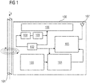
- FIG 1 illustrates a block diagram of a power network device 100, according to an embodiment of the present invention.
- the power network device 100 is physically disposable on a current carrying conductor 101.
- the current carrying conductor 101 carries a line current I L therewithin creating a magnetic field around itself in the direction shown in FIG 1 .
- the power network device 100 comprises a power harvesting module 102, a power transfer control module 108, an energy storage module 109, a sensor module 103, a parameter conditioning module 104, a processor 105, an indicator module 106, and a communication module 107 in operable communication with one another.
- the power harvested is used for powering one or more of the processor 105, the parameter conditioning module 104, the indicator module 106, and the communication module 107, of the power network device 300 via the power harvesting module 102 or via the energy storage module 109.
- FIG 2A illustrates a block diagram of a power harvesting module 102 configured as a switched mode power supply, in operable communication with a power transfer control module 108 and an energy storage module 109 of the power network device 100 shown in FIG 1 , according to an embodiment of the present invention.
- the power harvesting module 102 comprises an impedance regulation module 102A, a dynamic burden impedance 102B, and a voltage limiting module 102C, according to an embodiment of the present invention.
- the power harvesting module 102 comprises a flux concentrator such as a magnetic/non-magnetic core and a coil wound around the flux concentrator.
- the inductance L CC represents an inductance of the flux concentrator and the wound coil whereas the resistance R Coil represents a resistance of the wound coil.
- the flux concentrator with the coil wound around it is positioned near a bare or an insulated current carrying conductor 101.
- the flux concentrator is positioned surrounding the current carrying conductor 101 such that the current carrying conductor 101 passes through the flux concentrator, that is, through an air gap created within a core of the flux concentrator.
- the magnetic field created around the current carrying conductor 101 shown in FIG 1 is coupled with the coil wound around the flux concentrator thereby, inducing a flux in the flux concentrator.
- the current carrying conductor 101 is represented by an electrical equivalent circuit having a source voltage V S and an inductor L S through which a line current I L flows.
- the output voltage V op2 of the voltage limiting module 102C is then used for the powering the one or more modules of the power network device as well as charging the energy storage module 109.
- the power harvesting module 102 also comprises a current limiter C lim which comprises a power transistor such as a MOSFET and/or a resistor that protects the impedance regulation module from overcurrent conditions.
- the power transfer control module 108 comprises a comparator module 108A and a transfer switching module 108B.
- the transfer switching module 108B is connected across the coil wound on the flux concentrator.
- the comparator module 108A senses the voltage of the energy storage module 109 after charging and compares the same with the upper threshold level. When this voltage becomes equal to the upper threshold level, the transfer switching module 108B shorts the coil of the power harvesting module 102 to stop the power being harvested. Once the coil is short circuited, the modules of the power network device 102 draw their power from the energy storage module 109.
- the comparator module 108A senses the voltage of the energy storage module 109 while it is powering the modules of the power network device 100 and once it becomes equal to the lower threshold level, the transfer switching module 108B removes the short circuit applied across the coil in order for the power harvesting module 102 to start harvesting power from the current carrying conductor 101 once again.
- FIG 2B illustrates an electrical equivalent circuit diagram of the impedance regulation module 102A shown in FIG 2A .
- the impedance regulation module 102A controls transfer of power being harvested by the power harvesting module 102 using the induced voltage V ind and the line current I L , to the load connected thereto, that is, to one or modules of the power network device 100 shown in FIG 1 .
- the impedance regulation module 102A comprises a switching module 102D, a power detection module 102E, and a compensating impedance Z C .
- the impedance regulation module 102A operates in two states. First state of operation is when the power harvested based on the induced voltage V ind and the line current I L , is lesser than a predefined power threshold P T and second state of operation is when the power harvested is greater than or equal to the predefined power threshold P T . In the first state of operation, the power detection module 102E keeps the switching module 102D de-activated. The compensating impedance Z C remains to be connected in series with the R Coil .
- a reactive component X C of the compensating impedance Z C is in resonance with the reactive component X CC defined by the wound coil inductance L CC , thereby reducing effective source impedance Z source of the power harvesting module 102 equal to the coil resistance R Coil , as given in the equation below:
- Z source R Coil
- the power detection module 102E detects that the power harvested based on the induced voltage V ind and the line current I L , has equaled or exceeded the predefined power threshold P T .
- the power detection module 102E activates the switching module 102D such that the compensating impedance Z C is bypassed, thereby making the effective source impedance Z source dependent on the coil resistance R Coil and the wound coil inductance L CC , as given by the equation below:
- Z source ⁇ R coil 2 + X CC 2
- X CC 2 ⁇ f (L CC ) and f is the frequency of operation, for example, 50Hz.
- the power detection module 102E comprises a rectifier 102F, a transistor Q1, and a diode D1.
- the rectifier 102C converts an AC waveform of the induced voltage V ind into a single ended voltage waveform which is compared with a bypass voltage V byp .
- the bypass voltage V byp is a voltage required for activating the switching module 102A.
- the bypass voltage V byp is set based on the predefined power threshold P T .
- the bypass voltage V byp is selected such that the switching module 102D activates as soon as the bypass voltage V byp becomes equal to or greater than P T/ I L , in order to ensure the power being transferred to the load is within the predefined power threshold P T .
- the impedance regulation module 102A at any time instant maintains power harvested less than the predefined power threshold P T , that is, to maintain the induced voltage V ind less than P T /I L .
- V BE is the cut-off voltage for the transistor Q1 to conduct and V ref is the voltage required for the diode D1 to forward bias.
- V ref is the voltage required for the diode D1 to forward bias.
- the increase in source impedance Z source thus, limits the power being transferred to the load.
- the decrease in source impedance Z source thus, increases the power being transferred to the load.
- the impedance regulation module 102A detects power available at the source using current and/or voltage signatures, that is, the line current I L and the induced voltage V ind , and based on this detected power, dynamically changes source impedance Z source to create a resonance effect and increase power transferred to load at lower operating points, whereas decrease power transferred to load at higher operating points, thereby, increasing a range of operation, reducing overall weight, as well as stress experienced by downstream loads connected to the power harvesting module 102.
- FIGS 2C-2D illustrate a block diagram and an electrical equivalent circuit diagram of the dynamic burden impedance 102B shown in FIG 2A .
- FIG 2C illustrates a block diagram of the dynamic burden impedance 102B, wherein, a voltage V op1 , which is the output voltage of the impedance regulation module 102A shown in FIGS 2A , 2B , is applied across the dynamic burden impedance 102B.
- the dynamic burden impedance 102B comprises a voltage reference module 102G and a dynamic impedance module 102H in operable communication with each other.
- the dynamic burden impedance 102B acts a variable load in the power harvesting module 102 in order to maintain a constant output voltage V op1 irrespective of changes in the line current I L and the induced voltage V ind . This is achieved by shunting the increased current using the dynamic burden impedance 102B, thereby regulating flux induced in the core of the flux concentrator.
- FIG 2D illustrates an electrical equivalent diagram of the dynamic burden impedance 102B including the voltage reference module 102G and the dynamic impedance module 102H.
- the voltage reference module 102G includes Zener diodes D7, D10, D13, D6, D9 and D12 used to set a voltage threshold, that is, a limiting value at which the output voltage V op1 is to be regulated. Quantity of the Zener diodes and their ratings may be customized based on the voltage threshold required to be set.
- the voltage threshold is defined based on downstream electronics which is connected and/or powered by the power harvesting module 102.
- the dynamic impedance module 102H includes power transistors, that is, MOSFETs Q8, Q9 and Q6, Q7.
- Each of the pairs of these MOSFETs are connected to the Zener diodes D7, D10, D13 and D6, D9, D12 via PNP transistors Q5 and Q10 for operation in positive cycle and negative cycle respectively.
- the dynamic burden impedance thus limits the output voltage V op1 applied downstream.
- the additional current is mainly drawn by the MOSFETs Q8 and Q9 which are power devices and hence, are capable of handling larger power as compared to the Zener diodes D7, D10, and D13.
- the operation explained here is for the positive cycle operation and the negative cycle operation is the same with polarities reversed where the Zener diodes D6, D9, and D12 along with the PNP transistor Q10 and MOSFETs Q6 and Q7 come into operation.
- the dynamic impedance module 102H employs power MOSFETs Q7, Q8, Q9, and Q10, as dynamic burden resistors and regulates output voltage V op1 by changing V GS of the MOSFETs in comparison to the voltage threshold set using high precision low power Zener diodes D7, D10, D13, D6, D9, and D12.
- an additional voltage drop across source impedance is created which acts as a negative feedback control system thereby, avoiding flux increase and saturation of the flux concentrator of the power harvesting module 102.
- FIG 2E illustrates a graphical representation of voltage waveforms 102I, 102J, and 102K associated with an output voltage V oP1 of the dynamic burden impedance 102B shown in FIGS 2C-2D .
- the voltage waveforms 102I, 102J, and 102K are plotted with respect to time and current drawn by the dynamic impedance module 102H.
- the voltage waveform 102I represents an input voltage that is, the output voltage of the impedance regulation module 102A.
- the voltage waveform 102J represents the voltage limited by the dynamic burden impedance 102B beyond a voltage threshold of 37V which is achieved with a 36.3V Zener diode in combination with 0.7V V BE drop.
- the voltage waveform 102K represents the current drawn by the dynamic burden impedance 102B to maintain the output voltage V op1 constant.
- FIG 2F-2G illustrate a block diagram and an electrical equivalent circuit diagram of the voltage limiting module 102C shown in FIG 2A that regulates an output voltage V op2 of the power harvesting module 102, based on a predefined load voltage threshold to protect one or more modules of the power network device 100 being powered.
- FIG 2F illustrates a block diagram of the voltage limiting module 102C comprising a depletion MOSFET D MOS in a normally closed mode of operation in an operable connection with an impedance control module 102L set at a reference voltage equal to the load voltage threshold.
- the MOSFET D MOS is in a normally closed mode of operation, that is, when the input voltage is less than the reference voltage, the input voltage is passed to the load with minimal drop.
- FIG 2G illustrates an electrical equivalent circuit diagram of the voltage limiting module 102C comprising MOSFETs Q11 and Q13 as the MOSFET D MOS for positive and negative half cycles of an AC input voltage.
- the input voltage is passed through Q11 and it appears across the Zener D19 via the resistors R27 and R28.
- V300 If this voltage is less than the breakdown voltage of the Zener D19 then all the voltage appears across the Zener D19 and in turn at the emitter of transistor V300. As the base of V300 sees a stepped down version of this voltage, the V300 doesn't conduct. However, once the voltage becomes higher than the breakdown voltage of the Zener D19, the voltage is clamped by the Zener D19 whereas the voltage at the base of V300 increases as it is derived via a resistance divider and V300 conducts thereby, setting the transistor Q12 into conduction which in turn pulls down the gate voltage of the MOSFET Q11. With this, the drain-source resistance of Q11 increases resulting in a higher drop across Q11 and protecting the load connected at the output of the voltage limiting module 102C.
- the limiting voltage is independent of the MOSFET characteristics and only depends on transistor and Zener voltages. Therefore, the voltage limiting module 102C limits the output voltage V op2 to V lim thereby, protecting the downstream electronics.
- the voltage limiting module 102C shown in FIGS 2F and 2G can be employed for AC as well as DC sources with minor modifications in the components used.
- FIG 3 illustrates an electrical equivalent circuit diagram of a parameter conditioning module 104 of the power network device 100 shown in FIG 1 .
- the parameter conditioning module 104 in communication with the processor 105 of the power network device 100 shown in FIG 1 , dynamically amplifies one or more parameters using an amplifier module 104C based on one or more properties of a flux concentrator of the sensor module 103.
- the parameter conditioning module 104 comprises an AC coupler module 104A, an offset module 104B and the amplifier module 104C.
- the AC coupler module 104A receives an input, for example, the induced voltage V ind harvested by the coil wound flux concentrator of the sensor module 103.
- the coupler module 104A removes DC component associated with the induced voltage V ind .
- the AC component is then passed to the offset module 104B comprising a resistance divider designed so as to add a DC component predefined based on a reference voltage.
- the reference voltage is selected so as to ensure that a quiescent operating point of the amplifier module 104C accommodates entire dynamic range of the parameters being measured by the sensor module 103, and minimizes any distortion associated therewith.
- the offset module 104B on adding the predefined DC components clamps the input parameter, that is, the induced voltage V ind to a known DC operating point.
- the amplifier module 104C is a single stage amplifier comprising two or more MOSFETs, for example, M1, M2, etc., as shown in FIG 3 , which are switched on or off by the processor 105 so as to select an amplification factor, that is, a gain value with which the induced voltage V ind is amplified.
- the amplification factor is selected based on saturation tolerance of the flux concentrator core and/or a range of line current I L .
- the amplified induced voltage V ind is then passed to the processor 105 via an analog to digital converter (not shown) for further processing, for example, detection of a condition of the power network.
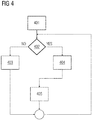
- FIG 4 is a process flow chart illustrating a method for dynamically conditioning one or more parameters measured by the power network device 100 shown in FIG 1 .
- the method disclosed herein employs the parameter conditioning module 104 shown in FIG 3 for dynamically conditioning the parameters measured.
- the method selects the highest amplification factor.
- the method verifies if the core of the flux concentrator of the sensor module 103 is saturated. If not, then at step 403 the amplifier module 104C of the parameter conditioning module 104 amplifies the parameter using the amplification factor. If yes, at step 404, the parameter conditioning module 104 reduces the amplification factor by one to the next lower amplification factor.
- the parameter conditioning module 104 selects the reduced amplification factor and repeats steps 402-404 so long as the core does not saturate.
- the process flow disclosed herein precludes need to track the changes in the line current I L and also manual intervention to select an amplification factor, thereby, avoiding calibration during installation and/or change in line current I L .
Abstract


Description
- The present invention relates to a heatsink free power network device. More particularly, the present invention relates to a wireless fault detection and indication device powered by an electromagnetic energy harvesting system having an increased range of operation and high measurement accuracy.
- The present invention claims the priority of European patent applications
EP 18192042.2 EP 18168232.9 US 16/003,360 - Typically, sensors are deployed in many regions of a power grid to sense the voltage and the current of transmission lines. A primary functionality of these sensors is to detect faults so that fault localization time is reduced thus reducing downtime of grids. Downstream sections of the grids carry very low currents, for example, about 3A whereas the upstream sections carry high currents up to about 600A. During occurrence of a fault, this current may go up to 1800A. These fault sensors thus, need to measure and operate with a wide dynamic range and are required to be designed so as to maximize power at lower line currents and minimize power as well as resultant heating at higher line currents. Conventional methods and systems limit power transfer at higher line currents by employing range extenders that limit voltage. However, these are suited for DC sources and their operation is largely temperature dependent thereby, rendering them inefficient for power constrained devices that may involve component variations. Moreover, these power network devices need to operate with a high reliability, for example having a functional life greater than ten years without maintenance for the entire duration of functional life since removing and reinstalling decreases the operating quality of grids.
- Furthermore, these fault sensors are mounted on existing transmission lines, due to which the fault data needs to be wirelessly transmitted to a base station. Moreover, as these sensors are mounted on existing transmission lines without disconnecting the lines to slide in the sensors, a flux concentrator core of the sensor, that harvests power from the transmission lines, has to be of a split configuration so as to form a clamp around the transmission line and enclose line current thereby, creating an air gap in the core. Such power being harvested is heavily dependent on the air gap as well as the mechanical variations associated with remote manual mounting onto the transmission lines. The harvested power is directly proportional to square of the line current flowing through it and therefore, demands a flux concentrator large enough to extract minimum power required for operating the sensor at the downstream sections of the grid. The harvested power needs to support the measurement of parameters as well as processing of the measurements. However, when the line current is high, power dissipation in the sensor increases thereby, producing a challenge for heat dissipation together with a wide dynamic range of operation.
- Achieving high accuracy measurements with the aforementioned power network devices that harvest energy electromagnetically from the line current poses a power consumption challenge. This in turn puts constraints on quantity, quality, and topologies of components that can be included in the electronics associated with such power network devices. Conventional methods and systems address the accuracy and component design challenge by employing multi-stage amplification or multiple amplifiers in parallel. However, this calls for higher number of components resulting in increased power consumption and costs associated with the design. Moreover, there is a possibility of errors increasing in cascade when multi-stage amplification is employed.
- Therefore, it is an object of the present invention to provide a heat sink free power network device of the aforementioned kind that offers a wide dynamic range of operation with high measurement accuracy, without increasing costs and design complexity associated therewith.
- The present invention disclosed herein achieves the aforementioned object by providing a power network device physically disposable on a current carrying conductor and comprising a sensor module, a processor, a power harvesting module, an energy storage module, and a power transfer control module, in operable communication with one another. The power harvesting module comprises an impedance regulation module, a dynamic burden impedance, and a voltage limiting module. The power network device disclosed herein harvests power from the current carrying conductor by harvesting an induced voltage proportional to a line current flowing in the current carrying conductor. According to an embodiment of the present invention, the current carrying conductor refers to a power line such as an overhead line or an underground cable of an electric grid, that is, a power transmission network and/or a power distribution network. According to an embodiment of the present invention, the power network device is a fault sensor indicator device. According to other embodiment of the present invention, the power network device is any device that detects and/or indicates a condition associated with the power network and is powered using electromagnetic energy harvesting, that is, using the line current flowing in the power lines.
- The sensor module measures one or more parameters associated with the current carrying conductor. The sensor module comprises a flux concentrator and at least one coil wound on the flux concentrator to measure the parameters. The parameters comprise, for example, a line current and a line voltage associated with the current carrying conductor. The processor detects a condition in the power network based on the parameters, sensed by the sensor module. The condition comprises, for example, a fault such as a line to line fault, a line to earth fault, a short circuit fault, etc., an unbalance in one or more of the parameters when compared to prescribed grid operating limits such as unbalance line voltage, unbalance line current, unbalance line phase, etc., isolation of a part of the power network, etc. The processor refers to any one of microprocessors, central processing unit (CPU) devices, finite state machines, microcontrollers, digital signal processors, an application specific integrated circuit (ASIC), a field-programmable gate array (FPGA), etc., or any combination thereof, capable of executing computer programs or a series of commands, instructions, or state transitions. The processor may also be implemented as a processor set comprising, for example, a general purpose microprocessor and a math or graphics coprocessor. The term processor is not used as a limiting term and may extend to a controller or a microcontroller.
- According to an embodiment of the present invention, the power network device comprises an indicator module that indicates the condition, for example, via an audio signal, an audio-visual signal, a visual signal, etc., such as by flashing light emitting diodes. According to an embodiment of the present invention, the power network device comprises a communication module communicating the condition and/or the parameters to an external system such as a communication hub at a substation. The communication module, for example, employs a Zigbee communication protocol.
- The power harvesting module harvests an induced voltage proportional to the line current, and generates power for powering one or more modules of the power network device, for example, at least the processor. The power harvesting module comprises a flux concentrator and at least one coil wound on the flux concentrator to harvest the induced voltage proportional to the line current. The flux concentrator converts electrical energy being harvested from a line current flowing in the current carrying conductor into magnetic energy in form of an electromagnetically induced flux. The coil wound on the flux concentrator, then converts this magnetic energy into an electrical equivalent in form of an induced voltage which in turn is used to generate power for powering one or more modules of the power network device. The coil is configured as an induction coil comprising a wire wound around the flux concentrator. In an embodiment of the present invention, the flux concentrator comprises a magnetic core. In another embodiment of the present invention, the flux concentrator comprises a non-magnetic core thereby producing an air-core flux concentrator. The coil couples an induced voltage proportional to a line current flowing in the current carrying conductor, for powering a load. Sinusoidally time-varying current flows in the current carrying conductor producing time-varying magnetic fields around the conductor. Windings of the coil positioned proximal to the current carrying conductor couple with the time-varying magnetic fields thereby producing an induced voltage therewithin. According to the present invention, the flux concentrator with the wound coil comprises a reactive component and the coil comprises a resistive component.
- The impedance regulation module of the power harvesting module dynamically regulates impedance in the power harvesting module for controlling transfer of power harvested using the induced voltage and the line current to the processor, the indicator module, and the parameter conditioning module. As used herein, the term "impedance" refers to a source impedance seen by the power harvesting module due to the flux concentrator and the coil of the power network device. For a time-varying sinusoidal current flowing in the current carrying conductor, a source impedance Zsource is calculated as sum of a reactance XCC offered by an inductive and/or a capacitive component of the wound coil with the flux concentrator, and a resistance RCoil of the coil. The power harvesting module harvests power using the induced voltage and the line current which are in turn affected by the source impedance Zsource. The impedance regulation module comprises a compensating impedance at least partially nullifying a reactance of a coil, that is, XCC of the power harvesting module when the power harvested is less than a predefined power threshold. Thus, the impedance regulation module dynamically regulates the source impedance Zsource. The compensating impedance of the impedance regulation module is selected based on the coil such that, a reactance XC of the compensating impedance at least partially nullifies the reactance XCC of the wound coil. Advantageously, the compensating impedance is in resonance with the source impedance Zsource, thereby, reducing the source impedance Zsource to a resistive component RCoil of the coil. This leads to maximum harvested power being transferred from the power harvesting module which in turn is used to power one or more modules of the power network device and is stored in the energy storage module of the power network device.
- The impedance regulation module comprises a switching module and a power detection module in operable communication with the compensating impedance. The power detection module detects the power harvested based on the induced voltage and the line current IL. Advantageously, the power detection module detects the power in real time. The power detection module at least partially includes the compensating impedance, in communication with the switching module, when the power harvested is less than a predefined power threshold. The switching module is an electronically controlled switch, for example, a relay whose coil is the control element, a solid state relay whose photodiode is the control element, etc. According to an embodiment of the present invention, the compensating impedance comprises two or more capacitors connected in series. In this embodiment, the power detection module along with the switching module includes one or more of the series connected capacitors into the power harvesting module. The power detection module excludes the compensating impedance when the power harvested is greater than a predefined power threshold and/or equal to the predefined power threshold. By excluding the compensating impedance, the power harvesting module ensures safety of the downstream electronics, thereby, increasing a range of harvesting of power from a varying line current while ensuring that power is limited within a prescribed range of safe operation of load connected thereto. The power threshold is defined based on power requirements of the load being driven by the power harvesting module, that is, one or more modules of the power network device, and the input power available that is harvested from the line current flowing in the current carrying conductor.
- The dynamic burden impedance of the power harvesting module is configured as a variable load regulating an output voltage of an impedance regulation module of the power harvesting module, based on a predefined voltage threshold to maintain flux induced in the power harvesting module. The dynamic burden impedance includes a voltage reference module and a dynamic impedance module in operable communication with one another. The voltage reference module defines the predefined voltage threshold for regulating the output voltage of the impedance regulation module. The predefined voltage threshold is selected based on one or more properties of the flux concentrator and the coil of the power harvesting module, including for example, a material and a geometry of the flux concentrator and winding elements, a saturation limit of the flux concentrator, and the output voltage of the impedance regulation module. The dynamic burden impedance comprises at least one power transistor selected based on the predefined voltage threshold.
- The voltage limiting module of the power harvesting module regulates an output voltage of the power harvesting module, based on a predefined load voltage threshold to protect one or more modules of the power harvesting module. The voltage limiting module employs a hardware impedance control module that regulates the output voltage by increasing and decreasing overall impedance of the power harvesting module based on the load voltage threshold. The load voltage threshold is defined based on power requirements of the load being powered. Advantageously, the dynamic burden impedance and the voltage limiting module are configured such that the dynamic burden impedance is a shunt voltage limiter allowing lower voltages, for example, lesser than or equal to about 80V to be applied downstream and the voltage limiting module is a series voltage limiter allowing voltages lesser than or equal to about 20V to be applied downstream. According to an embodiment of the present invention, the power harvesting module comprises a current limiter having for example, at least one power transistor. The current limiter protects the impedance regulation module from high line currents.
- The power network device comprises an energy storage module storing the harvested power. The energy storage module comprises one or more capacitors such as super capacitors selected based on requirements of the load being powered, that is, one or more modules of the power network device. The power network device comprises a power transfer control module selectively transferring the harvested power to one or more modules of the power network device, from the power harvesting module or the energy storage module. The power transfer control module comprises a comparator module and a transfer switching module. The comparator module compares the harvested power stored in the energy storage module with an upper threshold level and a lower threshold level. The transfer switching module applies a short circuit across a coil of the power harvesting module when the harvested power stored in the energy storage module equals the upper threshold level. The transfer switching module removes the short circuit across the coil when the harvested power stored in the energy storage module equals the lower threshold level. The lower threshold level is defined such that the stored power suffices power requirements of all the modules of the power network device drawing power from the power harvesting module based on their rated operating voltages. The upper threshold level is defined based on the storage capacity of the energy storage module as well as on the modules drawing power from the power harvesting module. For example, the lower threshold level is a minimum of all maximum rated voltages of the modules of the power network device whereas the upper threshold level is a maximum of all minimum rated voltages of the modules of the power network device. The transfer switching module is a fast switching and high current rating switch. Advantageously, power dissipated in the transfer switching module is negligible due to the coil being short circuited as a result of which heat sink size can be reduced and/or the heat sink can be eliminated thereby reducing costs associated with the power network device.
- The power transfer control module thus, operates in two modes comprising, a charging mode and a discharging mode. In the charging mode of operation, the power transfer control module allows the harvested power to be delivered to the one or more modules, for example, the processor, the indication module, the communication module, the parameter conditioning module, etc., of the power network device via the power harvesting module as well as to the energy storage module in order to store the harvested power therein. Once the harvested power stored in the energy storage module reaches the upper threshold level, the discharging mode of operation begins where the coil is shorted and input power being harvested is switched off. In this mode, the one or more modules being powered draw power from the energy storage module. As a result, the voltage across the energy storage module starts decreasing. The moment it becomes equal to the lower threshold level, the charging mode of operation begins. Thus, the power transfer control module dynamically changes the modes of operation by sensing source power availability and load power requirements at a given instant by using discrete components.
- The power network device comprises a parameter conditioning module dynamically conditioning the parameters. The parameter conditioning module in communication with the processor, dynamically amplifies the parameters using an amplifier module based on one or more properties of a flux concentrator of the sensor module. The properties comprise, for example, a saturation limit of the flux concentrator. The amplifier module is a single stage amplifier module configurable for a predefined range of amplification factors. The amplification factors are defined corresponding to the line current ranging from about 3A to about 1800A. Advantageously, the parameters especially corresponding to lower line currents, for example, from about 2A to about 40A, when amplified by the parameter conditioning module, remain unaffected by noise and other distortions if any, in the power harvesting module, thereby, increasing accuracy of measurement of the parameters. The parameter conditioning module selects a maximum amplification factor, that is, a highest gain band by default, and verifies whether the flux concentrator core of the sensor module has saturated as a result of the amplified parameter. If yes, the parameter conditioning module reduces the amplification factor, for example, to a next lower factor, else uses the same to amplify the measured parameters for further processing by the processor. Advantageously, the parameter conditioning module employs a single stage amplifier configurable with one or more of the predefined amplification factors, for dynamically measuring a wide range of parameters without affecting accuracy associated therewith and eliminating calibration requirements associated with changes in the line current once installed thereby, achieving lower power consumption and lower operational costs.
- The power harvesting module disclosed herein is configured as a switched mode power supply in communication with the power transfer control module and the energy storage module. Advantageously, the power harvesting module disclosed herein restricts heating of the power network device by achieving maximum power transfer at lower induced voltages and limited power transfer at higher induced voltages. The power harvesting module configured as the switched mode power supply also restricts overall heat dissipation in the power network device, thereby, allowing a heat sink-free device having a higher reliability, longer life of the harvesting coil, and operating in a wide dynamic range of line currents. The power network device disclosed herein includes a non-thermally conducting, that is a non-metallic, enclosure such as a plastic enclosure.
- The above-mentioned and other features of the invention will now be addressed with reference to the accompanying drawings of the present invention. The illustrated embodiments are intended to illustrate, but not limit the invention.
- The present invention is further described hereinafter with reference to illustrated embodiments shown in the accompanying drawings, in which:
- FIG 1
- illustrates a block diagram of a power network device, according to an embodiment of the present invention.
- FIG 2A
- illustrates a block diagram of a power harvesting module configured as a switched mode power supply, in operable communication with a power transfer control module and an energy storage module of the power network device shown in
FIG 1 , according to an embodiment of the present invention. - FIG 2B
- illustrates an electrical equivalent circuit diagram of the impedance regulation module shown in
FIG 2A . - FIGS 2C-2D
- illustrate a block diagram and an electrical equivalent circuit diagram of the dynamic burden impedance shown in
FIG 2A . - FIG 2E
- illustrates a graphical representation of voltage waveforms associated with an output voltage of the dynamic burden impedance shown in
FIGS 2C-2D . - FIG 2F-2G
- illustrate a block diagram and an electrical equivalent circuit diagram of the voltage limiting module shown in
FIG 2A . - FIG 3
- illustrates an electrical equivalent circuit diagram of a parameter conditioning module of the power network device shown in
FIG 1 . - FIG 4
- is a process flow chart illustrating a method for dynamically conditioning one or more parameters measured by the power network device shown in
FIG 1 . - Various embodiments are described with reference to the drawings, wherein like reference numerals are used to refer to like elements throughout. In the following description, for the purpose of explanation, numerous specific details are set forth in order to provide thorough understanding of one or more embodiments. It may be evident that such embodiments may be practiced without these specific details.
-
FIG 1 illustrates a block diagram of apower network device 100, according to an embodiment of the present invention. Thepower network device 100 is physically disposable on acurrent carrying conductor 101. Thecurrent carrying conductor 101 carries a line current IL therewithin creating a magnetic field around itself in the direction shown inFIG 1 . Thepower network device 100 comprises apower harvesting module 102, a powertransfer control module 108, anenergy storage module 109, asensor module 103, aparameter conditioning module 104, aprocessor 105, anindicator module 106, and acommunication module 107 in operable communication with one another. The power harvested is used for powering one or more of theprocessor 105, theparameter conditioning module 104, theindicator module 106, and thecommunication module 107, of the power network device 300 via thepower harvesting module 102 or via theenergy storage module 109. -
FIG 2A illustrates a block diagram of apower harvesting module 102 configured as a switched mode power supply, in operable communication with a powertransfer control module 108 and anenergy storage module 109 of thepower network device 100 shown inFIG 1 , according to an embodiment of the present invention. Thepower harvesting module 102 comprises animpedance regulation module 102A, adynamic burden impedance 102B, and avoltage limiting module 102C, according to an embodiment of the present invention. Thepower harvesting module 102 comprises a flux concentrator such as a magnetic/non-magnetic core and a coil wound around the flux concentrator. The inductance LCC represents an inductance of the flux concentrator and the wound coil whereas the resistance RCoil represents a resistance of the wound coil. The flux concentrator with the coil wound around it is positioned near a bare or an insulatedcurrent carrying conductor 101. For example, the flux concentrator is positioned surrounding thecurrent carrying conductor 101 such that thecurrent carrying conductor 101 passes through the flux concentrator, that is, through an air gap created within a core of the flux concentrator. The magnetic field created around thecurrent carrying conductor 101 shown inFIG 1 , is coupled with the coil wound around the flux concentrator thereby, inducing a flux in the flux concentrator. Thecurrent carrying conductor 101 is represented by an electrical equivalent circuit having a source voltage VS and an inductor LS through which a line current IL flows. The induced flux when coupled with the coil wound on the flux concentrator, produces an induced voltage Vind across the coil which is in turn is applied to theimpedance regulation module 102A, which in turn is applied to thedynamic source impedance 102B as Vop1 and to thevoltage limiting module 102C. The output voltage Vop2 of thevoltage limiting module 102C is then used for the powering the one or more modules of the power network device as well as charging theenergy storage module 109. Thepower harvesting module 102 also comprises a current limiter Clim which comprises a power transistor such as a MOSFET and/or a resistor that protects the impedance regulation module from overcurrent conditions. - The power
transfer control module 108 comprises acomparator module 108A and atransfer switching module 108B. Thetransfer switching module 108B is connected across the coil wound on the flux concentrator. Thecomparator module 108A senses the voltage of theenergy storage module 109 after charging and compares the same with the upper threshold level. When this voltage becomes equal to the upper threshold level, thetransfer switching module 108B shorts the coil of thepower harvesting module 102 to stop the power being harvested. Once the coil is short circuited, the modules of thepower network device 102 draw their power from theenergy storage module 109. Thecomparator module 108A senses the voltage of theenergy storage module 109 while it is powering the modules of thepower network device 100 and once it becomes equal to the lower threshold level, thetransfer switching module 108B removes the short circuit applied across the coil in order for thepower harvesting module 102 to start harvesting power from thecurrent carrying conductor 101 once again. -
FIG 2B illustrates an electrical equivalent circuit diagram of theimpedance regulation module 102A shown inFIG 2A . Theimpedance regulation module 102A controls transfer of power being harvested by thepower harvesting module 102 using the induced voltage Vind and the line current IL, to the load connected thereto, that is, to one or modules of thepower network device 100 shown inFIG 1 . Theimpedance regulation module 102A comprises aswitching module 102D, apower detection module 102E, and a compensating impedance ZC. - The
impedance regulation module 102A operates in two states. First state of operation is when the power harvested based on the induced voltage Vind and the line current IL, is lesser than a predefined power threshold PT and second state of operation is when the power harvested is greater than or equal to the predefined power threshold PT. In the first state of operation, thepower detection module 102E keeps theswitching module 102D de-activated. The compensating impedance ZC remains to be connected in series with the RCoil. A reactive component XC of the compensating impedance ZC is in resonance with the reactive component XCC defined by the wound coil inductance LCC, thereby reducing effective source impedance Zsource of thepower harvesting module 102 equal to the coil resistance RCoil, as given in the equation below:
- This ensures maximum power transfer to load when the induced voltage Vind is below a predefined power threshold.
- In the second state of operation, the
power detection module 102E detects that the power harvested based on the induced voltage Vind and the line current IL, has equaled or exceeded the predefined power threshold PT. Thepower detection module 102E activates theswitching module 102D such that the compensating impedance ZC is bypassed, thereby making the effective source impedance Zsource dependent on the coil resistance RCoil and the wound coil inductance LCC, as given by the equation below:
- Where XCC = 2Πf (LCC) and f is the frequency of operation, for example, 50Hz.
- The
power detection module 102E comprises arectifier 102F, a transistor Q1, and a diode D1. Therectifier 102C converts an AC waveform of the induced voltage Vind into a single ended voltage waveform which is compared with a bypass voltage Vbyp. The bypass voltage Vbyp is a voltage required for activating theswitching module 102A. The bypass voltage Vbyp is set based on the predefined power threshold PT. For example, if the load being powered by thepower harvesting system 100 has an operating power range of up to PT Watts then the bypass voltage Vbyp is selected such that theswitching module 102D activates as soon as the bypass voltage Vbyp becomes equal to or greater than PT/IL, in order to ensure the power being transferred to the load is within the predefined power threshold PT. Theimpedance regulation module 102A at any time instant maintains power harvested less than the predefined power threshold PT, that is, to maintain the induced voltage Vind less than PT/IL. - In order to set the bypass voltage Vbyp according to the predefined power threshold PT the diode D1 and the transistor Q1 are selected such that:

- Where VBE is the cut-off voltage for the transistor Q1 to conduct and Vref is the voltage required for the diode D1 to forward bias. When the induced voltage Vind becomes equal to the base emitter voltage VBE, the transistor Q1 conducts. Further as the induced voltage Vind increases to equal sum of the base emitter voltage VBE and the voltage Vref, which is equal to the set bypass voltage Vbyp, a control element of the
switching module 102D activates, thereby bypassing the compensating impedance ZC and increasing the effective source impedance Zsource, given by the equation below:
- The increase in source impedance Zsource thus, limits the power being transferred to the load.
- When the induced voltage Vind starts decreasing and becomes lesser than the bypass voltage Vbyp the
switching module 102D gets de-activated. The induced voltage Vind decreases further to equal the base emitter voltage VBE, the diode D1 comes out of its forward bias operation region. The induced voltage Vind decreases further below the base emitter voltage VBE, the transistor Q1 stops conducting, thereby bringing the compensating impedance ZC back in connection thereby, decreasing the effective source impedance Zsource, given by the equation below:
- The decrease in source impedance Zsource thus, increases the power being transferred to the load.
- Thus, the
impedance regulation module 102A, detects power available at the source using current and/or voltage signatures, that is, the line current IL and the induced voltage Vind, and based on this detected power, dynamically changes source impedance Zsource to create a resonance effect and increase power transferred to load at lower operating points, whereas decrease power transferred to load at higher operating points, thereby, increasing a range of operation, reducing overall weight, as well as stress experienced by downstream loads connected to thepower harvesting module 102. -
FIGS 2C-2D illustrate a block diagram and an electrical equivalent circuit diagram of thedynamic burden impedance 102B shown inFIG 2A .FIG 2C illustrates a block diagram of thedynamic burden impedance 102B, wherein, a voltage Vop1, which is the output voltage of theimpedance regulation module 102A shown inFIGS 2A ,2B , is applied across thedynamic burden impedance 102B. Thedynamic burden impedance 102B comprises avoltage reference module 102G and adynamic impedance module 102H in operable communication with each other. Thedynamic burden impedance 102B acts a variable load in thepower harvesting module 102 in order to maintain a constant output voltage Vop1 irrespective of changes in the line current IL and the induced voltage Vind. This is achieved by shunting the increased current using thedynamic burden impedance 102B, thereby regulating flux induced in the core of the flux concentrator. -
FIG 2D illustrates an electrical equivalent diagram of thedynamic burden impedance 102B including thevoltage reference module 102G and thedynamic impedance module 102H. Thevoltage reference module 102G includes Zener diodes D7, D10, D13, D6, D9 and D12 used to set a voltage threshold, that is, a limiting value at which the output voltage Vop1 is to be regulated. Quantity of the Zener diodes and their ratings may be customized based on the voltage threshold required to be set. The voltage threshold is defined based on downstream electronics which is connected and/or powered by thepower harvesting module 102. Thedynamic impedance module 102H includes power transistors, that is, MOSFETs Q8, Q9 and Q6, Q7. Each of the pairs of these MOSFETs are connected to the Zener diodes D7, D10, D13 and D6, D9, D12 via PNP transistors Q5 and Q10 for operation in positive cycle and negative cycle respectively. During a positive cycle of operation, when an input voltage, that is, the secondary voltage, rises above the voltage threshold defined by a combined breakdown voltage of the Zener diodes D7, D10, and D13, and the VBE drop of the PNP transistor Q5, then the Q5 conducts. Thus, the voltage threshold is defined by the equation given below:
- With this a proportional current flows on the collector of Q5 increasing the VGS voltage of the MOSFETs Q8 and Q9. As this VGS voltage increases, the RDS of the MOSFETs decrease. As RDS decreases additional current is drawn from the source, thereby, increasing drop across source, resulting, in a decrease in the voltage across the Zener diodes D7, D10, and D13, and therefore the VBE of the PNP transistor Q5, thereby reducing, the collector current of Q5 and VGS voltage of the MOSFETs Q8 and Q9. As this VGS voltage decreases, the RDS of the MOSFETs increases thereby, reducing current drawn from the source. This in turn reduces the drop across source, thus, bringing back the operation state to an original state. The dynamic burden impedance thus limits the output voltage Vop1 applied downstream. The additional current is mainly drawn by the MOSFETs Q8 and Q9 which are power devices and hence, are capable of handling larger power as compared to the Zener diodes D7, D10, and D13. The operation explained here is for the positive cycle operation and the negative cycle operation is the same with polarities reversed where the Zener diodes D6, D9, and D12 along with the PNP transistor Q10 and MOSFETs Q6 and Q7 come into operation. Thus, the
dynamic impedance module 102H employs power MOSFETs Q7, Q8, Q9, and Q10, as dynamic burden resistors and regulates output voltage Vop1 by changing VGS of the MOSFETs in comparison to the voltage threshold set using high precision low power Zener diodes D7, D10, D13, D6, D9, and D12. By dynamically changing the burden impedance and thereby drawing additional current from the source, an additional voltage drop across source impedance is created which acts as a negative feedback control system thereby, avoiding flux increase and saturation of the flux concentrator of thepower harvesting module 102. -
FIG 2E illustrates a graphical representation ofvoltage waveforms dynamic burden impedance 102B shown inFIGS 2C-2D . Thevoltage waveforms dynamic impedance module 102H. The voltage waveform 102I represents an input voltage that is, the output voltage of theimpedance regulation module 102A. Thevoltage waveform 102J represents the voltage limited by thedynamic burden impedance 102B beyond a voltage threshold of 37V which is achieved with a 36.3V Zener diode in combination with 0.7V VBE drop. Thevoltage waveform 102K represents the current drawn by thedynamic burden impedance 102B to maintain the output voltage Vop1 constant. -
FIG 2F-2G illustrate a block diagram and an electrical equivalent circuit diagram of thevoltage limiting module 102C shown inFIG 2A that regulates an output voltage Vop2 of thepower harvesting module 102, based on a predefined load voltage threshold to protect one or more modules of thepower network device 100 being powered.FIG 2F illustrates a block diagram of thevoltage limiting module 102C comprising a depletion MOSFET DMOS in a normally closed mode of operation in an operable connection with animpedance control module 102L set at a reference voltage equal to the load voltage threshold. When the MOSFET DMOS is in a normally closed mode of operation, that is, when the input voltage is less than the reference voltage, the input voltage is passed to the load with minimal drop. When the input voltage starts increasing, it is applied as feedback through theimpedance control module 102L to the MOSFET DMOS thereby, increasing the resistance of the MOSFET DMOS and limiting the voltage seen by the load represented by the resistance RLoad to a value defined by the reference voltage.FIG 2G illustrates an electrical equivalent circuit diagram of thevoltage limiting module 102C comprising MOSFETs Q11 and Q13 as the MOSFET DMOS for positive and negative half cycles of an AC input voltage. Considering a positive half cycle operation, when an input voltage is applied at Q11 and Q11 is in its normally closed mode, that is, VGS is zero and Q11 is conducting, the input voltage is passed through Q11 and it appears across the Zener D19 via the resistors R27 and R28. If this voltage is less than the breakdown voltage of the Zener D19 then all the voltage appears across the Zener D19 and in turn at the emitter of transistor V300. As the base of V300 sees a stepped down version of this voltage, the V300 doesn't conduct. However, once the voltage becomes higher than the breakdown voltage of the Zener D19, the voltage is clamped by the Zener D19 whereas the voltage at the base of V300 increases as it is derived via a resistance divider and V300 conducts thereby, setting the transistor Q12 into conduction which in turn pulls down the gate voltage of the MOSFET Q11. With this, the drain-source resistance of Q11 increases resulting in a higher drop across Q11 and protecting the load connected at the output of thevoltage limiting module 102C. The limiting voltage, that is, the reference voltage as shown inFIG 2F is set using below equation:
- Thus, the limiting voltage is independent of the MOSFET characteristics and only depends on transistor and Zener voltages. Therefore, the
voltage limiting module 102C limits the output voltage Vop2 to Vlim thereby, protecting the downstream electronics. Thevoltage limiting module 102C shown inFIGS 2F and2G can be employed for AC as well as DC sources with minor modifications in the components used. -
FIG 3 illustrates an electrical equivalent circuit diagram of aparameter conditioning module 104 of thepower network device 100 shown inFIG 1 . Theparameter conditioning module 104 in communication with theprocessor 105 of thepower network device 100 shown inFIG 1 , dynamically amplifies one or more parameters using anamplifier module 104C based on one or more properties of a flux concentrator of thesensor module 103. Theparameter conditioning module 104 comprises anAC coupler module 104A, an offsetmodule 104B and theamplifier module 104C. TheAC coupler module 104A receives an input, for example, the induced voltage Vind harvested by the coil wound flux concentrator of thesensor module 103. Thecoupler module 104A removes DC component associated with the induced voltage Vind. This is because the DC component is typically unknown and/or varies greatly which may lead to saturation of the flux concentrator when amplified with higher gain values. The AC component is then passed to the offsetmodule 104B comprising a resistance divider designed so as to add a DC component predefined based on a reference voltage. The reference voltage is selected so as to ensure that a quiescent operating point of theamplifier module 104C accommodates entire dynamic range of the parameters being measured by thesensor module 103, and minimizes any distortion associated therewith. Thus, the offsetmodule 104B on adding the predefined DC components clamps the input parameter, that is, the induced voltage Vind to a known DC operating point. Theamplifier module 104C is a single stage amplifier comprising two or more MOSFETs, for example, M1, M2, etc., as shown inFIG 3 , which are switched on or off by theprocessor 105 so as to select an amplification factor, that is, a gain value with which the induced voltage Vind is amplified. The amplification factor is selected based on saturation tolerance of the flux concentrator core and/or a range of line current IL. The amplified induced voltage Vind, is then passed to theprocessor 105 via an analog to digital converter (not shown) for further processing, for example, detection of a condition of the power network. -
FIG 4 is a process flow chart illustrating a method for dynamically conditioning one or more parameters measured by thepower network device 100 shown inFIG 1 . The method disclosed herein employs theparameter conditioning module 104 shown inFIG 3 for dynamically conditioning the parameters measured. Atstep 401, the method selects the highest amplification factor. At step, 402, the method verifies if the core of the flux concentrator of thesensor module 103 is saturated. If not, then atstep 403 theamplifier module 104C of theparameter conditioning module 104 amplifies the parameter using the amplification factor. If yes, atstep 404, theparameter conditioning module 104 reduces the amplification factor by one to the next lower amplification factor. Atstep 405, theparameter conditioning module 104 selects the reduced amplification factor and repeats steps 402-404 so long as the core does not saturate. The process flow disclosed herein precludes need to track the changes in the line current IL and also manual intervention to select an amplification factor, thereby, avoiding calibration during installation and/or change in line current IL. - The foregoing examples have been provided merely for the purpose of explanation and are in no way to be construed as limiting of the present invention disclosed herein. While the invention has been described with reference to various embodiments, it is understood that the words, which have been used herein, are words of description and illustration, rather than words of limitation. Further, although the invention has been described herein with reference to particular means, materials, and embodiments, the invention is not intended to be limited to the particulars disclosed herein; rather, the invention extends to all functionally equivalent structures, methods and uses, such as are within the scope of the appended claims. Those skilled in the art, having the benefit of the teachings of this specification, may affect numerous modifications thereto and changes may be made without departing from the scope and spirit of the invention in its aspects.
-
- 100 power network device
- 101 current carrying conductor
- IL line current
- LCC inductance offered by coil and the flux concentrator
- VS source voltage
- LS inductance of the current carrying conductor
- RCoil resistance offered by coil
- Clim current limiter
- Vop1 output voltage of impedance regulation module
- Vop2 output voltage of power harvesting module
- 102 power harvesting module
- 102A impedance regulation module (Dyn src impedance)
- 102B dynamic burden impedance (shunt V_lim/flux limiting)
- 102C voltage limiting module (series V_lim)
- 102D switching module
- 102E power detection module
- 102F rectifier
- 102G voltage reference module
- 102H dynamic impedance module
- 102I, 102J, 102K voltage waveforms associated with dynamic burden impedance
- 102L Impedance control module
- 103 sensor module
- 104 parameter conditioning module (AFE)
- 104A coupler module
- 104B offset module
- 104C amplifier module
- 105 processor/controller
- 106 indicator module
- 107 communication module
- 108 power transfer control module
- 108A comparator module
- 108Bq transfer switching module
- 109 energy storage module
Claims (15)
- A power network device (100) physically disposable on a current carrying conductor (101), the power network device (100) comprising:- a sensor module (103) configured to measure one or more parameters associated with the current carrying conductor (101);- a processor (105) configured to detect a condition in the power distribution network based on the one or more parameters; and- a power harvesting module (102) configured to harvest power by harvesting an induced voltage (Vind) proportional to the line current (IL), for powering one or more modules of the power network device (100), wherein the power harvesting module (102) comprises:∘ an impedance regulation module (102A);∘ a dynamic burden impedance (102B); and∘ a voltage limiting module (102C);- an energy storage module (109) configured to store the harvested power; and- a power transfer control module (108) configured to selectively transfer the harvested power to the one or more modules of the power network device (100), from one of the power harvesting module (102) and the energy storage module (109).
- The power network device (100) according to claim 1, wherein the power harvesting module (102) comprises a flux concentrator and at least one coil wound on the flux concentrator to harvest the induced voltage (Vind) proportional to the line current (IL).
- The power network device (100) according to claim 1, wherein the impedance regulation module (102A) is configured to dynamically regulate impedance in the power harvesting module (102) for controlling transfer of power harvested using the induced voltage (Vind) and the line current (IL), to at least the processor (105).
- The power network device (100) according to any one of the claims 1 and 3, wherein the impedance regulation module (102A) comprises a compensating impedance (Zc) at least partially nullifying a reactance of a coil of the power harvesting module (102) when power harvested using the induced voltage (Vind) and the line current (IL), is less than a predefined power threshold.
- The power network device (100) according to claim 1, wherein the dynamic burden impedance (102B) is configured as a variable load to regulate an output voltage (Vop1) of the impedance regulation module (102A), based on a predefined voltage threshold to maintain flux induced in the power harvesting module (102).
- The power network device (100) according to claim 1, wherein the voltage limiting module (102C) is configured to regulate an output voltage (Vop2) of the power harvesting module (102), based on a predefined load voltage threshold to protect at least the processor (105) being powered.
- The power network device (100) according to claim 1, wherein the power harvesting module (102) is configured as a switched mode power supply.
- The power network device (100) according to claim 1, wherein the sensor module (102) comprises a flux concentrator and at least one coil wound on the flux concentrator to measure the one or more parameters.
- The power network device (100) according to any one of the previous claims further comprising, a parameter conditioning module (104) configured to dynamically condition the one or more parameters.
- The power network device (100) according to claim 9, wherein the parameter conditioning module (104) in communication with a processor (105), is configured to dynamically amplify one or more parameters measured by a sensor module (103) using an amplifier module (104C) based on one or more properties of a flux concentrator of the sensor module (103).
- The power network device (100) according to claim 10, wherein the amplifier module (104C) is a single-stage amplifier module configurable for a predefined range of amplification factors.
- The power network device (100) according to claim 1, wherein the power transfer control module (108) comprises:- a comparator module (108A) configured to compare the harvested power stored in the energy storage module (109) with an upper threshold level and a lower threshold level; and- a transfer switching module (108B) configured to apply a short circuit across a coil of the power harvesting module (102) when the harvested power stored in the energy storage module (109) equals the upper threshold level, and remove the short circuit across the coil when the harvested power stored in the energy storage module (109) equals the lower threshold level.
- The power network device (100) according to any one of the previous claims further comprising, a communication module (107) configured to communicate one or more of the condition and the one or more parameters to an external system.
- The power network device (100) according to any one of the previous claims further comprising, an indicator module (106) configured to indicate the condition detected by the processor (105) .
- The power network device (100) according to any one of the previous claims is a fault sensor indicator device.
Applications Claiming Priority (3)
| Application Number | Priority Date | Filing Date | Title |
|---|---|---|---|
| EP18168232.9A EP3557728A1 (en) | 2018-04-19 | 2018-04-19 | Dynamic power harvesting system |
| US16/003,360 US10298208B1 (en) | 2018-06-08 | 2018-06-08 | Dynamic impedance system for an increased range of operation of an instrument transformer |
| EP18192042.2A EP3557729B1 (en) | 2018-04-19 | 2018-08-31 | Power network device |
Publications (2)
| Publication Number | Publication Date |
|---|---|
| EP3557730A1 true EP3557730A1 (en) | 2019-10-23 |
| EP3557730B1 EP3557730B1 (en) | 2021-03-10 |
Family
ID=63452581
Family Applications (1)
| Application Number | Title | Priority Date | Filing Date |
|---|---|---|---|
| EP18192530.6A Active EP3557730B1 (en) | 2018-04-19 | 2018-09-04 | Power network device |
Country Status (1)
| Country | Link |
|---|---|
| EP (1) | EP3557730B1 (en) |
Cited By (2)
| Publication number | Priority date | Publication date | Assignee | Title |
|---|---|---|---|---|
| WO2022149980A1 (en) * | 2021-01-08 | 2022-07-14 | Use System Engineering Holding B.V. | Transfer pick-up circuit |
| CN116632797A (en) * | 2023-03-23 | 2023-08-22 | 周口睿勤电子科技有限公司 | Power electronic direct current protection device and installation method thereof |
Citations (4)
| Publication number | Priority date | Publication date | Assignee | Title |
|---|---|---|---|---|
| US20150091385A1 (en) * | 2013-09-27 | 2015-04-02 | Texas Instruments Incorporated | Power harvest architecture for near field communication devices |
| US20160049800A1 (en) * | 2013-04-30 | 2016-02-18 | Yazaki Corporation | Power supply system and resonance circuit |
| US20160209454A1 (en) * | 2015-01-19 | 2016-07-21 | Patrick McCammon | Wireless Power Line Sensor |
| US20170179732A1 (en) * | 2015-12-22 | 2017-06-22 | Cooper Technologies Company | Dynamic Tuning for Harvesting Energy from Current Transformers |
-
2018
- 2018-09-04 EP EP18192530.6A patent/EP3557730B1/en active Active
Patent Citations (4)
| Publication number | Priority date | Publication date | Assignee | Title |
|---|---|---|---|---|
| US20160049800A1 (en) * | 2013-04-30 | 2016-02-18 | Yazaki Corporation | Power supply system and resonance circuit |
| US20150091385A1 (en) * | 2013-09-27 | 2015-04-02 | Texas Instruments Incorporated | Power harvest architecture for near field communication devices |
| US20160209454A1 (en) * | 2015-01-19 | 2016-07-21 | Patrick McCammon | Wireless Power Line Sensor |
| US20170179732A1 (en) * | 2015-12-22 | 2017-06-22 | Cooper Technologies Company | Dynamic Tuning for Harvesting Energy from Current Transformers |
Cited By (3)
| Publication number | Priority date | Publication date | Assignee | Title |
|---|---|---|---|---|
| WO2022149980A1 (en) * | 2021-01-08 | 2022-07-14 | Use System Engineering Holding B.V. | Transfer pick-up circuit |
| NL2027290B1 (en) * | 2021-01-08 | 2022-07-22 | Use System Eng Holding B V | Transfer pick-up circuit |
| CN116632797A (en) * | 2023-03-23 | 2023-08-22 | 周口睿勤电子科技有限公司 | Power electronic direct current protection device and installation method thereof |
Also Published As
| Publication number | Publication date |
|---|---|
| EP3557730B1 (en) | 2021-03-10 |
Similar Documents
| Publication | Publication Date | Title |
|---|---|---|
| US8896334B2 (en) | System for measuring soft starter current and method of making same | |
| US8649193B2 (en) | Leakage current reducing apparatus | |
| JP2018087783A (en) | Electricity leakage detection device | |
| JPS5816459B2 (en) | Motor winding temperature detection device | |
| EP3557730B1 (en) | Power network device | |
| EP2665929A1 (en) | A wind turbine fault detection circuit and method | |
| EP2831992B1 (en) | Medical imaging device | |
| US11418023B2 (en) | Current protection circuit and method for high voltage system | |
| CN103827676A (en) | System for measuring current and method of making same | |
| CN113287180B (en) | System and method for regulating power drawn from an Inductive Power Harvester (IPH) | |
| EP3557729B1 (en) | Power network device | |
| US11356012B2 (en) | Transmission and distribution system with electric shock protection function and method of operating the same | |
| EP3432460B1 (en) | Power converter | |
| US10992176B2 (en) | Dynamic power harvesting system | |
| WO2014014544A1 (en) | Method and apparatus of locating current sensors | |
| JPH01311864A (en) | Switching system stablizing electric source device | |
| EP2806278B1 (en) | Current divider for extended current measurement | |
| CN112383214A (en) | IGBT parallel current-sharing circuit | |
| US8941956B2 (en) | Switching ground tether circuit | |
| US11740265B1 (en) | Signal conditioning circuit | |
| CN105683043B (en) | A kind of protection equipment for being used for preventing the upstream circuit of power supply module | |
| CN213461535U (en) | IGBT parallel current-sharing circuit | |
| CN116997804A (en) | Current sensing circuit and current measurement system for measuring current in electrical wire | |
| CN201569690U (en) | Current detection device for air conditioner controller | |
| CN209881385U (en) | Power module with input overvoltage protection function |
Legal Events
| Date | Code | Title | Description |
|---|---|---|---|
| PUAI | Public reference made under article 153(3) epc to a published international application that has entered the european phase |
Free format text: ORIGINAL CODE: 0009012 |
|
| STAA | Information on the status of an ep patent application or granted ep patent |
Free format text: STATUS: THE APPLICATION HAS BEEN PUBLISHED |
|
| AK | Designated contracting states |
Kind code of ref document: A1 Designated state(s): AL AT BE BG CH CY CZ DE DK EE ES FI FR GB GR HR HU IE IS IT LI LT LU LV MC MK MT NL NO PL PT RO RS SE SI SK SM TR |
|
| AX | Request for extension of the european patent |
Extension state: BA ME |
|
| STAA | Information on the status of an ep patent application or granted ep patent |
Free format text: STATUS: REQUEST FOR EXAMINATION WAS MADE |
|
| 17P | Request for examination filed |
Effective date: 20200327 |
|
| RBV | Designated contracting states (corrected) |
Designated state(s): AL AT BE BG CH CY CZ DE DK EE ES FI FR GB GR HR HU IE IS IT LI LT LU LV MC MK MT NL NO PL PT RO RS SE SI SK SM TR |
|
| GRAP | Despatch of communication of intention to grant a patent |
Free format text: ORIGINAL CODE: EPIDOSNIGR1 |
|
| STAA | Information on the status of an ep patent application or granted ep patent |
Free format text: STATUS: GRANT OF PATENT IS INTENDED |
|
| RIC1 | Information provided on ipc code assigned before grant |
Ipc: H02J 50/10 20160101AFI20200908BHEP |
|
| INTG | Intention to grant announced |
Effective date: 20201013 |
|
| STAA | Information on the status of an ep patent application or granted ep patent |
Free format text: STATUS: GRANT OF PATENT IS INTENDED |
|
| GRAS | Grant fee paid |
Free format text: ORIGINAL CODE: EPIDOSNIGR3 |
|
| GRAA | (expected) grant |
Free format text: ORIGINAL CODE: 0009210 |
|
| STAA | Information on the status of an ep patent application or granted ep patent |
Free format text: STATUS: THE PATENT HAS BEEN GRANTED |
|
| AK | Designated contracting states |
Kind code of ref document: B1 Designated state(s): AL AT BE BG CH CY CZ DE DK EE ES FI FR GB GR HR HU IE IS IT LI LT LU LV MC MK MT NL NO PL PT RO RS SE SI SK SM TR |
|
| REG | Reference to a national code |
Ref country code: GB Ref legal event code: FG4D |
|
| REG | Reference to a national code |
Ref country code: AT Ref legal event code: REF Ref document number: 1370892 Country of ref document: AT Kind code of ref document: T Effective date: 20210315 Ref country code: CH Ref legal event code: EP |
|
| REG | Reference to a national code |
Ref country code: IE Ref legal event code: FG4D |
|
| REG | Reference to a national code |
Ref country code: DE Ref legal event code: R096 Ref document number: 602018013635 Country of ref document: DE |
|
| REG | Reference to a national code |
Ref country code: LT Ref legal event code: MG9D |
|
| PG25 | Lapsed in a contracting state [announced via postgrant information from national office to epo] |
Ref country code: BG Free format text: LAPSE BECAUSE OF FAILURE TO SUBMIT A TRANSLATION OF THE DESCRIPTION OR TO PAY THE FEE WITHIN THE PRESCRIBED TIME-LIMIT Effective date: 20210610 Ref country code: FI Free format text: LAPSE BECAUSE OF FAILURE TO SUBMIT A TRANSLATION OF THE DESCRIPTION OR TO PAY THE FEE WITHIN THE PRESCRIBED TIME-LIMIT Effective date: 20210310 Ref country code: GR Free format text: LAPSE BECAUSE OF FAILURE TO SUBMIT A TRANSLATION OF THE DESCRIPTION OR TO PAY THE FEE WITHIN THE PRESCRIBED TIME-LIMIT Effective date: 20210611 Ref country code: HR Free format text: LAPSE BECAUSE OF FAILURE TO SUBMIT A TRANSLATION OF THE DESCRIPTION OR TO PAY THE FEE WITHIN THE PRESCRIBED TIME-LIMIT Effective date: 20210310 Ref country code: LT Free format text: LAPSE BECAUSE OF FAILURE TO SUBMIT A TRANSLATION OF THE DESCRIPTION OR TO PAY THE FEE WITHIN THE PRESCRIBED TIME-LIMIT Effective date: 20210310 |
|
| REG | Reference to a national code |
Ref country code: AT Ref legal event code: MK05 Ref document number: 1370892 Country of ref document: AT Kind code of ref document: T Effective date: 20210310 |
|
| REG | Reference to a national code |
Ref country code: NL Ref legal event code: MP Effective date: 20210310 |
|
| REG | Reference to a national code |
Ref country code: NO Ref legal event code: T2 Effective date: 20210310 |
|
| PG25 | Lapsed in a contracting state [announced via postgrant information from national office to epo] |
Ref country code: RS Free format text: LAPSE BECAUSE OF FAILURE TO SUBMIT A TRANSLATION OF THE DESCRIPTION OR TO PAY THE FEE WITHIN THE PRESCRIBED TIME-LIMIT Effective date: 20210310 Ref country code: LV Free format text: LAPSE BECAUSE OF FAILURE TO SUBMIT A TRANSLATION OF THE DESCRIPTION OR TO PAY THE FEE WITHIN THE PRESCRIBED TIME-LIMIT Effective date: 20210310 Ref country code: SE Free format text: LAPSE BECAUSE OF FAILURE TO SUBMIT A TRANSLATION OF THE DESCRIPTION OR TO PAY THE FEE WITHIN THE PRESCRIBED TIME-LIMIT Effective date: 20210310 |
|
| PG25 | Lapsed in a contracting state [announced via postgrant information from national office to epo] |
Ref country code: NL Free format text: LAPSE BECAUSE OF FAILURE TO SUBMIT A TRANSLATION OF THE DESCRIPTION OR TO PAY THE FEE WITHIN THE PRESCRIBED TIME-LIMIT Effective date: 20210310 |
|
| PG25 | Lapsed in a contracting state [announced via postgrant information from national office to epo] |
Ref country code: EE Free format text: LAPSE BECAUSE OF FAILURE TO SUBMIT A TRANSLATION OF THE DESCRIPTION OR TO PAY THE FEE WITHIN THE PRESCRIBED TIME-LIMIT Effective date: 20210310 Ref country code: CZ Free format text: LAPSE BECAUSE OF FAILURE TO SUBMIT A TRANSLATION OF THE DESCRIPTION OR TO PAY THE FEE WITHIN THE PRESCRIBED TIME-LIMIT Effective date: 20210310 Ref country code: SM Free format text: LAPSE BECAUSE OF FAILURE TO SUBMIT A TRANSLATION OF THE DESCRIPTION OR TO PAY THE FEE WITHIN THE PRESCRIBED TIME-LIMIT Effective date: 20210310 Ref country code: AT Free format text: LAPSE BECAUSE OF FAILURE TO SUBMIT A TRANSLATION OF THE DESCRIPTION OR TO PAY THE FEE WITHIN THE PRESCRIBED TIME-LIMIT Effective date: 20210310 |
|
| PG25 | Lapsed in a contracting state [announced via postgrant information from national office to epo] |
Ref country code: IS Free format text: LAPSE BECAUSE OF FAILURE TO SUBMIT A TRANSLATION OF THE DESCRIPTION OR TO PAY THE FEE WITHIN THE PRESCRIBED TIME-LIMIT Effective date: 20210710 Ref country code: RO Free format text: LAPSE BECAUSE OF FAILURE TO SUBMIT A TRANSLATION OF THE DESCRIPTION OR TO PAY THE FEE WITHIN THE PRESCRIBED TIME-LIMIT Effective date: 20210310 Ref country code: SK Free format text: LAPSE BECAUSE OF FAILURE TO SUBMIT A TRANSLATION OF THE DESCRIPTION OR TO PAY THE FEE WITHIN THE PRESCRIBED TIME-LIMIT Effective date: 20210310 Ref country code: PT Free format text: LAPSE BECAUSE OF FAILURE TO SUBMIT A TRANSLATION OF THE DESCRIPTION OR TO PAY THE FEE WITHIN THE PRESCRIBED TIME-LIMIT Effective date: 20210712 Ref country code: PL Free format text: LAPSE BECAUSE OF FAILURE TO SUBMIT A TRANSLATION OF THE DESCRIPTION OR TO PAY THE FEE WITHIN THE PRESCRIBED TIME-LIMIT Effective date: 20210310 |
|
| REG | Reference to a national code |
Ref country code: DE Ref legal event code: R097 Ref document number: 602018013635 Country of ref document: DE |
|
| PLBE | No opposition filed within time limit |
Free format text: ORIGINAL CODE: 0009261 |
|
| STAA | Information on the status of an ep patent application or granted ep patent |
Free format text: STATUS: NO OPPOSITION FILED WITHIN TIME LIMIT |
|
| PG25 | Lapsed in a contracting state [announced via postgrant information from national office to epo] |
Ref country code: ES Free format text: LAPSE BECAUSE OF FAILURE TO SUBMIT A TRANSLATION OF THE DESCRIPTION OR TO PAY THE FEE WITHIN THE PRESCRIBED TIME-LIMIT Effective date: 20210310 Ref country code: DK Free format text: LAPSE BECAUSE OF FAILURE TO SUBMIT A TRANSLATION OF THE DESCRIPTION OR TO PAY THE FEE WITHIN THE PRESCRIBED TIME-LIMIT Effective date: 20210310 Ref country code: AL Free format text: LAPSE BECAUSE OF FAILURE TO SUBMIT A TRANSLATION OF THE DESCRIPTION OR TO PAY THE FEE WITHIN THE PRESCRIBED TIME-LIMIT Effective date: 20210310 |
|
| 26N | No opposition filed |
Effective date: 20211213 |
|
| PG25 | Lapsed in a contracting state [announced via postgrant information from national office to epo] |
Ref country code: SI Free format text: LAPSE BECAUSE OF FAILURE TO SUBMIT A TRANSLATION OF THE DESCRIPTION OR TO PAY THE FEE WITHIN THE PRESCRIBED TIME-LIMIT Effective date: 20210310 |
|
| REG | Reference to a national code |
Ref country code: CH Ref legal event code: PL |
|
| REG | Reference to a national code |
Ref country code: BE Ref legal event code: MM Effective date: 20210930 |
|
| PG25 | Lapsed in a contracting state [announced via postgrant information from national office to epo] |
Ref country code: IS Free format text: LAPSE BECAUSE OF FAILURE TO SUBMIT A TRANSLATION OF THE DESCRIPTION OR TO PAY THE FEE WITHIN THE PRESCRIBED TIME-LIMIT Effective date: 20210710 Ref country code: MC Free format text: LAPSE BECAUSE OF FAILURE TO SUBMIT A TRANSLATION OF THE DESCRIPTION OR TO PAY THE FEE WITHIN THE PRESCRIBED TIME-LIMIT Effective date: 20210310 |
|
| PG25 | Lapsed in a contracting state [announced via postgrant information from national office to epo] |
Ref country code: LU Free format text: LAPSE BECAUSE OF NON-PAYMENT OF DUE FEES Effective date: 20210904 Ref country code: IE Free format text: LAPSE BECAUSE OF NON-PAYMENT OF DUE FEES Effective date: 20210904 Ref country code: FR Free format text: LAPSE BECAUSE OF NON-PAYMENT OF DUE FEES Effective date: 20210930 Ref country code: BE Free format text: LAPSE BECAUSE OF NON-PAYMENT OF DUE FEES Effective date: 20210930 |
|
| PG25 | Lapsed in a contracting state [announced via postgrant information from national office to epo] |
Ref country code: LI Free format text: LAPSE BECAUSE OF NON-PAYMENT OF DUE FEES Effective date: 20210930 Ref country code: CH Free format text: LAPSE BECAUSE OF NON-PAYMENT OF DUE FEES Effective date: 20210930 |
|
| PG25 | Lapsed in a contracting state [announced via postgrant information from national office to epo] |
Ref country code: CY Free format text: LAPSE BECAUSE OF FAILURE TO SUBMIT A TRANSLATION OF THE DESCRIPTION OR TO PAY THE FEE WITHIN THE PRESCRIBED TIME-LIMIT Effective date: 20210310 |
|
| PG25 | Lapsed in a contracting state [announced via postgrant information from national office to epo] |
Ref country code: HU Free format text: LAPSE BECAUSE OF FAILURE TO SUBMIT A TRANSLATION OF THE DESCRIPTION OR TO PAY THE FEE WITHIN THE PRESCRIBED TIME-LIMIT; INVALID AB INITIO Effective date: 20180904 |
|
| PGFP | Annual fee paid to national office [announced via postgrant information from national office to epo] |
Ref country code: NO Payment date: 20230906 Year of fee payment: 6 Ref country code: IT Payment date: 20230920 Year of fee payment: 6 |
|
| PGFP | Annual fee paid to national office [announced via postgrant information from national office to epo] |
Ref country code: GB Payment date: 20231009 Year of fee payment: 6 |
|
| PGFP | Annual fee paid to national office [announced via postgrant information from national office to epo] |
Ref country code: DE Payment date: 20231120 Year of fee payment: 6 |