EP3553886A1 - Antenna and antenna module - Google Patents
Antenna and antenna module Download PDFInfo
- Publication number
- EP3553886A1 EP3553886A1 EP19167684.0A EP19167684A EP3553886A1 EP 3553886 A1 EP3553886 A1 EP 3553886A1 EP 19167684 A EP19167684 A EP 19167684A EP 3553886 A1 EP3553886 A1 EP 3553886A1
- Authority
- EP
- European Patent Office
- Prior art keywords
- antenna
- dielectric substrate
- metal conductor
- conductor plate
- ground
- Prior art date
- Legal status (The legal status is an assumption and is not a legal conclusion. Google has not performed a legal analysis and makes no representation as to the accuracy of the status listed.)
- Withdrawn
Links
Images






Classifications
-
- H—ELECTRICITY
- H01—ELECTRIC ELEMENTS
- H01Q—ANTENNAS, i.e. RADIO AERIALS
- H01Q9/00—Electrically-short antennas having dimensions not more than twice the operating wavelength and consisting of conductive active radiating elements
- H01Q9/04—Resonant antennas
- H01Q9/0407—Substantially flat resonant element parallel to ground plane, e.g. patch antenna
-
- H—ELECTRICITY
- H01—ELECTRIC ELEMENTS
- H01Q—ANTENNAS, i.e. RADIO AERIALS
- H01Q1/00—Details of, or arrangements associated with, antennas
- H01Q1/48—Earthing means; Earth screens; Counterpoises
-
- H—ELECTRICITY
- H01—ELECTRIC ELEMENTS
- H01Q—ANTENNAS, i.e. RADIO AERIALS
- H01Q19/00—Combinations of primary active antenna elements and units with secondary devices, e.g. with quasi-optical devices, for giving the antenna a desired directional characteristic
- H01Q19/10—Combinations of primary active antenna elements and units with secondary devices, e.g. with quasi-optical devices, for giving the antenna a desired directional characteristic using reflecting surfaces
- H01Q19/104—Combinations of primary active antenna elements and units with secondary devices, e.g. with quasi-optical devices, for giving the antenna a desired directional characteristic using reflecting surfaces using a substantially flat reflector for deflecting the radiated beam, e.g. periscopic antennas
-
- H—ELECTRICITY
- H01—ELECTRIC ELEMENTS
- H01Q—ANTENNAS, i.e. RADIO AERIALS
- H01Q1/00—Details of, or arrangements associated with, antennas
- H01Q1/12—Supports; Mounting means
- H01Q1/22—Supports; Mounting means by structural association with other equipment or articles
- H01Q1/2283—Supports; Mounting means by structural association with other equipment or articles mounted in or on the surface of a semiconductor substrate as a chip-type antenna or integrated with other components into an IC package
Definitions
- the disclosures herein relate to an antenna and an antenna module.
- Antennas for transmitting and receiving radio waves are used in wireless communication. There are needs for an antenna capable of transmitting radio waves over as large a distance as possible and an antenna capable of receiving weak radio waves.
- An antenna is required to have not only an increased gain but also an improved directivity in order to transmit radio waves over as large a distance as possible and to receive weak radio waves.
- An antenna having a complex shape and a large size is not easy to handle, and is not suitable for provision in a portable device.
- antenna module in which an antenna is connected to an electronic circuit for generating radio waves to be transmitted from the antenna and connected to a signal processing circuit for processing radio wave signals received by the antenna. Size reduction is also required for such an antenna module.
- an antenna includes a dielectric substrate, an antenna element formed on a first surface of the dielectric substrate, a ground element formed on a second surface of the dielectric substrate, and a metal conductor plate disposed over, and at a spaced distance from, the first surface of the dielectric substrate, the metal conductor plate being larger than the ground element.
- a small antenna having such a shape that is easy to handle and having a satisfactory directivity is provided.
- Fig. 1A is a top view of the patch antenna 10.
- Fig. 1B is a cross-sectional view of the patch antenna 10.
- Fig. 2 is an axonometric view of the patch antenna 10.
- the patch antenna 10 includes an insulating dielectric substrate 11, an antenna element 12 disposed on a surface 11a of the dielectric substrate 11, and a ground element 13 disposed on a surface 11b of the dielectric substrate 11.
- the antenna element 12 and the ground element 13 are metal films that are electrically conductive.
- the ground element 13 is coupled to a ground potential.
- the antenna element 12, which receives a feed power, serves as a radiation plane for radiating radio waves.
- the dielectric substrate 11 is a square plate with a side of 15 mm and a thickness of 0.5 mm, which is made of a glass epoxy resin or the like having a relative permittivity of approximately 4.7.
- the antenna element 12 is a square shape with a side of 3 mm, and is formed at the center of the surface 11a.
- the ground element 13 is a square shape with a side of 15 mm disposed over the entirety of the surface 11b.
- the antenna element 12 and the ground element 13 may be made of copper foils with a thickness of 40 micrometers, for example.
- the patch antenna 10 is designed for a frequency of 24 GHz.
- ⁇ being the wavelength of a 24-GHz radio wave
- the length of a side of the antenna element 12, which may be set to ⁇ /2, is set to 3 mm with consideration for the effect of wavelength reduction resulting from the relative permittivity of the dielectric substrate 11.
- Simulation performed with respect to the patch antenna 10 revealed the presence of directivity as illustrated in Fig. 3 , in which radio waves are stronger in the positive Z direction that is on the same side as where the antenna element 12 is disposed.
- the gain of radio waves in the positive Z direction is approximately +5 dBi.
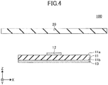
- Fig. 4 is a cross-sectional view of the antenna 100.
- Fig. 5 is an axonometric view of the antenna 100.
- the antenna 100 is configured such that a metal conductor plate 20 is situated on the positive Z side of the patch antenna 10.
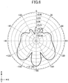
- the metal conductor plate 20 is a plate made of a conductive metal material such as copper (Cu), aluminum (Al), or stainless. Simulation performed with respect to the antenna 100 revealed the presence of directivity as illustrated in Fig. 6 , in which radio waves are stronger in the negative Z direction opposite from where the antenna element 12 is disposed.
- the gain of radio waves in the negative Z direction is approximately +10 dBi.
- the antenna 100 has a directivity pointing to the opposite direction from where the antenna element 12 is disposed, and also has a stronger gain.
- the metal conductor plate 20 may have holes or slits, except for the area situated directly above the antenna element 12.
- Simulation was conducted with respect to the antenna 100 illustrated in Fig. 7 under the conditions of varying size of the metal conductor plate 20 and under the conditions of varying distance between the patch antenna 10 and the metal conductor plate 20.
- the simulation conducted under the conditions of varying size of the metal conductor plate 20 will be described first.
- the simulations were conducted with respect to the square metal conductor plates 20 having differing side lengths L as follows: 15mm, 20mm, and 25.
- a distance D between the patch antenna 10 and the metal conductor plate 20 in the Z direction is 0.5 mm.
- the gain in the positive Z direction is approximately +5 dBi, which is about the same as in the case of no metal conductor plate 20 being provided.
- the gain in the negative Z direction is also +5 dBi.
- the gain in the positive Z direction decreases, and the gain in the negative Z direction increases.
- the gain in the positive Z direction is approximately -10 dBi
- the gain in the negative Z direction is approximately +10 dBi.
- the metal conductor plate 20 is approximately the same size as the dielectric substrate 11 and the ground element 13.
- the gain in the positive Z direction is approximately the same as in the case in which the no metal conductor plate 20 is provided, and is also approximately the same as the gain in the negative Z direction.
- the metal conductor plate 20 is made larger than the dielectric substrate 11 and the ground element 13, which increases directivity in the negative Z direction.
- the above description has been given with respect to the case in which the metal conductor plate 20 is a square. The same applies in the case of a rectangle.
- the metal conductor plate 20 is a rectangle of 15 mm by 20 mm, the advantage of increasing directivity in the negative Z direction may similarly be provided.
- the simulations conducted under the conditions of differing distance between the patch antenna 10 and the metal conductor plate 20 will be described in the following.
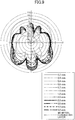
- the metal conductor plate 20 was a square with a side length L of 25 mm. Simulations were conducted with respect to differing distances D in the Z direction between the patch antenna 10 and the metal conductor plate 20 as follows: 0.2 mm, 0.3 mm, 0.4 mm, 0.5 mm, 0.7 mm, 1.0 mm, 1.5 mm, 2.0 mm, 2.5 mm, 3.0 mm, 4.0 mm, and 5.0 mm. The results of the simulations are shown in Fig. 9 .
- the gain in the negative Z direction decreases when the distance between the patch antenna 10 and the metal conductor plate 20 is below 0.3 mm or above 3.0 mm. Accordingly, the distance D between the patch antenna 10 and the metal conductor plate 20 is preferably greater than or equal to 0.3 mm and less than or equal to 3.0 mm.
- the wavelength ⁇ for a frequency of 24 GHz is 12 mm, which means that the distance D between the patch antenna 10 and the metal conductor plate 20 is preferably greater than or equal to ⁇ /40 and less than or equal to ⁇ /4.
- the antenna 100 of the present embodiment has the patch antenna 10 and the metal conductor plate 20 such that the metal conductor plate 20 is a plate shape.
- the antenna 100 is easy to install, and the size of the apparatus for which the antenna 100 is installed does not have to be large. Improving the directivity of an antenna may also be achieved by use of a structure in which the metal conductor plate has a curved surface, for example. With such a structure, however, the size of the antenna increases due to its curved surface. Further, since the metal conductor plate needs to be shaped into a curved form, the number of process steps increases, which results in a cost increase.
- the metal conductor plate 20 of the present embodiment is flat, which allows the apparatus to be smaller scale than in the case of a curved-surface metal conductor plate. Further, there is no increase in the number of process steps, which results in low production cost.
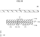
- the antenna module 201 has an antenna formed with a circuit substrate that includes multilayered interconnections.
- a conductor layer serving as the ground element 13 is formed inside a circuit substrate 210.
- Dielectric layers 210a and 210b are formed on the respective surfaces of the ground element 13.
- the antenna element 12 is disposed on a surface of the dielectric layer 210a.
- Electronic components 211, 212, and 213 are mounted on a surface of the dielectric layer 210b.
- the antenna element 12 and the electronic component 212 for supplying a radio frequency signal to the antenna element 12 are coupled to each other through a penetrating electrode 214.
- the electronic component 212 feeds power to the antenna element 12 through the penetrating electrode 214.
- the flat metal conductor plate 20 is disposed over the surface of the dielectric layer 210a on which the antenna element 12 is formed.
- the ground element 13 situated between the antenna element 12 and the electronic components 211, 212, and 213 is coupled to a ground potential, so that noise generated by the electronic components 211, 212, and 213 such as electromagnetic waves is blocked by the ground element 13 so as not to affect the antenna element 12.
- the dielectric layers 210a and 210b, the antenna element 12, the ground element 13, and the metal conductor plate 20 constitute an antenna.
- This configuration of the antenna module 201 allows the electronic component 211 and part of the antenna of the present embodiment to be incorporated into a single circuit substrate 210, which serves to provide a small-scale antenna module 201. Accordingly, the antenna module 201 having a high directivity is reduced in size.
- the antenna module 202 includes the patch antenna 10 and a circuit substrate 220.
- the electronic components 211, 212, and 213 are mounted on a surface 221a of the circuit substrate 220.
- a ground pattern 222 is formed on the entirety of a surface 221b of the circuit substrate 220.
- the ground pattern 222 is made of a metal material such as Cu.
- the ground pattern 222 of the antenna module 202 serves as the metal conductor plate of the antenna.
- the electronic component 212 mounted on the surface 221a to supply a signal to the antenna element 12 is coupled to the antenna element 12 through interconnections which are not shown.
- the ground element 13 formed on the surface 11b of the dielectric substrate 11 and the ground pattern 222 are coupled to each other through interconnections which are not shown.
- the surface 11a of the dielectric substrate 11 and the surface 221b of the circuit substrate 220 face each other, and the dielectric substrate 11 and the circuit substrate 220 are connected to each other through connect pins 231 situated inside spacers 232, with the spacers 232 placed between the dielectric substrate 11 and the circuit substrate 220.
- the distance between the dielectric substrate 11 and the circuit substrate 220 is kept to a fixed length by the spacers 232.
- the ground pattern 222 and the antenna element 12 face each other, and the ground pattern 222 coupled to the ground potential is situated between the antenna element 12 and the electronic components 211, 212, and 213. Noise generated by the electronic components 211, 212, and 213 such as electromagnetic waves is blocked by the ground pattern 222 so as not to affect the antenna element 12.
Landscapes
- Waveguide Aerials (AREA)
- Aerials With Secondary Devices (AREA)
- Details Of Aerials (AREA)
Abstract
Description
- The disclosures herein relate to an antenna and an antenna module.
- Antennas for transmitting and receiving radio waves are used in wireless communication. There are needs for an antenna capable of transmitting radio waves over as large a distance as possible and an antenna capable of receiving weak radio waves.
- An antenna is required to have not only an increased gain but also an improved directivity in order to transmit radio waves over as large a distance as possible and to receive weak radio waves. An antenna having a complex shape and a large size is not easy to handle, and is not suitable for provision in a portable device.
- There is a certain type of antenna module in which an antenna is connected to an electronic circuit for generating radio waves to be transmitted from the antenna and connected to a signal processing circuit for processing radio wave signals received by the antenna. Size reduction is also required for such an antenna module.
-
- [Patent Document 1] Japanese Patent Application Publication No.
2004-266618 - [Patent Document 2] Japanese Patent Application Publication No.
H7-50505 - It is a general object of the present invention to provide an antenna that substantially obviates one or more problems caused by the limitations and disadvantages of the related art.
- According to an embodiment, an antenna includes a dielectric substrate, an antenna element formed on a first surface of the dielectric substrate, a ground element formed on a second surface of the dielectric substrate, and a metal conductor plate disposed over, and at a spaced distance from, the first surface of the dielectric substrate, the metal conductor plate being larger than the ground element.
- According to at least one embodiment, a small antenna having such a shape that is easy to handle and having a satisfactory directivity is provided.
- Other objects and further features of the present invention will be apparent from the following detailed description when read in conjunction with the accompanying drawings, in which:
-
Figs. 1A and 1B are drawings illustrating the structure of a patch antenna; -
Fig. 2 is an axonometric view of the patch antenna; -
Fig. 3 is a drawing illustrating the characteristics of the patch antenna; -
Fig. 4 is a drawing illustrating the structure of an antenna according to an embodiment; -
Fig. 5 is an axonometric view of the antenna according to the embodiment; -
Fig. 6 is a drawing illustrating the characteristics of the antenna according to the embodiment; -
Fig. 7 is a drawing illustrating a simulation model of the antenna according to the embodiment; -
Fig. 8 is a drawing illustrating characteristics obtained by antenna simulation; -
Fig. 9 is a drawing illustrating characteristics obtained by antenna simulation; -
Fig. 10 is a drawing illustrating the structure of an antenna module according to an embodiment; and -
Fig. 11 is a drawing illustrating the structure of the antenna module according to the embodiment. - In the following, embodiments for implementing the invention will be described. The same members or the like are referred to by the same numerals, and a description thereof will be omitted.
- In the following, a
patch antenna 10 will be described.Fig. 1A is a top view of thepatch antenna 10.Fig. 1B is a cross-sectional view of thepatch antenna 10.Fig. 2 is an axonometric view of thepatch antenna 10. - The
patch antenna 10 includes an insulatingdielectric substrate 11, anantenna element 12 disposed on asurface 11a of thedielectric substrate 11, and aground element 13 disposed on asurface 11b of thedielectric substrate 11. Theantenna element 12 and theground element 13 are metal films that are electrically conductive. Theground element 13 is coupled to a ground potential. Theantenna element 12, which receives a feed power, serves as a radiation plane for radiating radio waves. - The
dielectric substrate 11 is a square plate with a side of 15 mm and a thickness of 0.5 mm, which is made of a glass epoxy resin or the like having a relative permittivity of approximately 4.7. Theantenna element 12 is a square shape with a side of 3 mm, and is formed at the center of thesurface 11a. Theground element 13 is a square shape with a side of 15 mm disposed over the entirety of thesurface 11b. Theantenna element 12 and theground element 13 may be made of copper foils with a thickness of 40 micrometers, for example. - The
patch antenna 10 is designed for a frequency of 24 GHz. With λ being the wavelength of a 24-GHz radio wave, the length of a side of theantenna element 12, which may be set to λ/2, is set to 3 mm with consideration for the effect of wavelength reduction resulting from the relative permittivity of thedielectric substrate 11. Simulation performed with respect to thepatch antenna 10 revealed the presence of directivity as illustrated inFig. 3 , in which radio waves are stronger in the positive Z direction that is on the same side as where theantenna element 12 is disposed. The gain of radio waves in the positive Z direction is approximately +5 dBi. - In the following, an
antenna 100 according to the present embodiment will be described with reference toFig. 4 andFig. 5 .Fig. 4 is a cross-sectional view of theantenna 100.Fig. 5 is an axonometric view of theantenna 100. Theantenna 100 is configured such that ametal conductor plate 20 is situated on the positive Z side of thepatch antenna 10. Themetal conductor plate 20 is a plate made of a conductive metal material such as copper (Cu), aluminum (Al), or stainless. Simulation performed with respect to theantenna 100 revealed the presence of directivity as illustrated inFig. 6 , in which radio waves are stronger in the negative Z direction opposite from where theantenna element 12 is disposed. The gain of radio waves in the negative Z direction is approximately +10 dBi. - Namely, the
antenna 100 has a directivity pointing to the opposite direction from where theantenna element 12 is disposed, and also has a stronger gain. Themetal conductor plate 20 may have holes or slits, except for the area situated directly above theantenna element 12. - Simulation was conducted with respect to the
antenna 100 illustrated inFig. 7 under the conditions of varying size of themetal conductor plate 20 and under the conditions of varying distance between thepatch antenna 10 and themetal conductor plate 20. - The simulation conducted under the conditions of varying size of the
metal conductor plate 20 will be described first. The simulations were conducted with respect to the squaremetal conductor plates 20 having differing side lengths L as follows: 15mm, 20mm, and 25. A distance D between thepatch antenna 10 and themetal conductor plate 20 in the Z direction is 0.5 mm. - The results of the simulations are shown in
Fig. 8 . In the case of the length L of the side of themetal conductor plate 20 being 15 mm, the gain in the positive Z direction is approximately +5 dBi, which is about the same as in the case of nometal conductor plate 20 being provided. The gain in the negative Z direction is also +5 dBi. - As the size of the
metal conductor plate 20 increases, however, the gain in the positive Z direction decreases, and the gain in the negative Z direction increases. In the case of the length L of the side of themetal conductor plate 20 being 25 mm, the gain in the positive Z direction is approximately -10 dBi, and the gain in the negative Z direction is approximately +10 dBi. - In the case of the length L of the side of the
metal conductor plate 20 being 15 mm, themetal conductor plate 20 is approximately the same size as thedielectric substrate 11 and theground element 13. In this case, the gain in the positive Z direction is approximately the same as in the case in which the nometal conductor plate 20 is provided, and is also approximately the same as the gain in the negative Z direction. - In the present embodiment, the
metal conductor plate 20 is made larger than thedielectric substrate 11 and theground element 13, which increases directivity in the negative Z direction. The above description has been given with respect to the case in which themetal conductor plate 20 is a square. The same applies in the case of a rectangle. When themetal conductor plate 20 is a rectangle of 15 mm by 20 mm, the advantage of increasing directivity in the negative Z direction may similarly be provided. - The simulations conducted under the conditions of differing distance between the
patch antenna 10 and themetal conductor plate 20 will be described in the following. Themetal conductor plate 20 was a square with a side length L of 25 mm. Simulations were conducted with respect to differing distances D in the Z direction between thepatch antenna 10 and themetal conductor plate 20 as follows: 0.2 mm, 0.3 mm, 0.4 mm, 0.5 mm, 0.7 mm, 1.0 mm, 1.5 mm, 2.0 mm, 2.5 mm, 3.0 mm, 4.0 mm, and 5.0 mm. The results of the simulations are shown inFig. 9 . - As illustrated in
Fig. 9 , the gain in the negative Z direction decreases when the distance between thepatch antenna 10 and themetal conductor plate 20 is below 0.3 mm or above 3.0 mm. Accordingly, the distance D between thepatch antenna 10 and themetal conductor plate 20 is preferably greater than or equal to 0.3 mm and less than or equal to 3.0 mm. The wavelength λ for a frequency of 24 GHz is 12 mm, which means that the distance D between thepatch antenna 10 and themetal conductor plate 20 is preferably greater than or equal to λ/40 and less than or equal to λ/4. - The
antenna 100 of the present embodiment has thepatch antenna 10 and themetal conductor plate 20 such that themetal conductor plate 20 is a plate shape. With this arrangement, theantenna 100 is easy to install, and the size of the apparatus for which theantenna 100 is installed does not have to be large. Improving the directivity of an antenna may also be achieved by use of a structure in which the metal conductor plate has a curved surface, for example. With such a structure, however, the size of the antenna increases due to its curved surface. Further, since the metal conductor plate needs to be shaped into a curved form, the number of process steps increases, which results in a cost increase. Themetal conductor plate 20 of the present embodiment is flat, which allows the apparatus to be smaller scale than in the case of a curved-surface metal conductor plate. Further, there is no increase in the number of process steps, which results in low production cost. - In the following, an
antenna module 201 of the present embodiment will be described by referring toFig. 10 . Theantenna module 201 has an antenna formed with a circuit substrate that includes multilayered interconnections. A conductor layer serving as theground element 13 is formed inside acircuit substrate 210.Dielectric layers ground element 13. - The
antenna element 12 is disposed on a surface of thedielectric layer 210a.Electronic components dielectric layer 210b. Theantenna element 12 and theelectronic component 212 for supplying a radio frequency signal to theantenna element 12 are coupled to each other through a penetratingelectrode 214. Theelectronic component 212 feeds power to theantenna element 12 through the penetratingelectrode 214. The flatmetal conductor plate 20 is disposed over the surface of thedielectric layer 210a on which theantenna element 12 is formed. - In the
antenna module 201, theground element 13 situated between theantenna element 12 and theelectronic components electronic components ground element 13 so as not to affect theantenna element 12. - In the
antenna module 201 illustrated inFig. 10 , thedielectric layers antenna element 12, theground element 13, and themetal conductor plate 20 constitute an antenna. This configuration of theantenna module 201 allows theelectronic component 211 and part of the antenna of the present embodiment to be incorporated into asingle circuit substrate 210, which serves to provide a small-scale antenna module 201. Accordingly, theantenna module 201 having a high directivity is reduced in size. - In the following, an
antenna module 202 of the present embodiment will be described by referring toFig. 11 . Theantenna module 202 includes thepatch antenna 10 and acircuit substrate 220. Theelectronic components surface 221a of thecircuit substrate 220. Aground pattern 222 is formed on the entirety of asurface 221b of thecircuit substrate 220. Theground pattern 222 is made of a metal material such as Cu. Theground pattern 222 of theantenna module 202 serves as the metal conductor plate of the antenna. - The
electronic component 212 mounted on thesurface 221a to supply a signal to theantenna element 12 is coupled to theantenna element 12 through interconnections which are not shown. Theground element 13 formed on thesurface 11b of thedielectric substrate 11 and theground pattern 222 are coupled to each other through interconnections which are not shown. - In the
antenna module 202, thesurface 11a of thedielectric substrate 11 and thesurface 221b of thecircuit substrate 220 face each other, and thedielectric substrate 11 and thecircuit substrate 220 are connected to each other through connectpins 231 situated insidespacers 232, with thespacers 232 placed between thedielectric substrate 11 and thecircuit substrate 220. With this arrangement, the distance between thedielectric substrate 11 and thecircuit substrate 220 is kept to a fixed length by thespacers 232. - In the
antenna module 202, theground pattern 222 and theantenna element 12 face each other, and theground pattern 222 coupled to the ground potential is situated between theantenna element 12 and theelectronic components electronic components ground pattern 222 so as not to affect theantenna element 12. - Further, although a description has been given with respect to one or more embodiments of the present invention, the contents of such a description do not limit the scope of the invention.
- The present application is based on and claims priority to Japanese patent application No.
2018-075215 filed on April 10, 2018
Claims (4)
- An antenna, comprising:a dielectric substrate;an antenna element formed on a first surface of the dielectric substrate;a ground element formed on a second surface of the dielectric substrate; anda metal conductor plate disposed over, and at a spaced distance from, the first surface of the dielectric substrate, the metal conductor plate being larger than the ground element.
- The antenna as claimed in claim 1, wherein the metal conductor plate is coupled to a ground potential.
- An antenna module, comprising:a dielectric substrate having a conductor layer embedded therein, the conductor layer serving as a ground element;an antenna element formed on a first surface of the dielectric substrate;an electronic component mounted on a second surface of the dielectric substrate; anda metal conductor plate disposed over, and at a spaced distance from, the first surface of the dielectric substrate, the metal conductor plate being larger than the ground element.
- An antenna module, comprising:a dielectric substrate;an antenna element formed on a first surface of the dielectric substrate;a ground element formed on a second surface of the dielectric substrate;a circuit substrate having an electronic component mounted on a first surface thereof; anda ground pattern formed on a second surface of the circuit substrate, the ground pattern being larger than the ground element,wherein the first surface of the dielectric substrate faces the second surface of the circuit substrate.
Applications Claiming Priority (1)
| Application Number | Priority Date | Filing Date | Title |
|---|---|---|---|
| JP2018075215A JP2019186741A (en) | 2018-04-10 | 2018-04-10 | Antenna and antenna modular |
Publications (1)
| Publication Number | Publication Date |
|---|---|
| EP3553886A1 true EP3553886A1 (en) | 2019-10-16 |
Family
ID=66102001
Family Applications (1)
| Application Number | Title | Priority Date | Filing Date |
|---|---|---|---|
| EP19167684.0A Withdrawn EP3553886A1 (en) | 2018-04-10 | 2019-04-05 | Antenna and antenna module |
Country Status (3)
| Country | Link |
|---|---|
| US (2) | US11133590B2 (en) |
| EP (1) | EP3553886A1 (en) |
| JP (1) | JP2019186741A (en) |
Cited By (1)
| Publication number | Priority date | Publication date | Assignee | Title |
|---|---|---|---|---|
| EP4318806A1 (en) | 2022-08-01 | 2024-02-07 | Sick Ag | Modular antenna for an rfid reader |
Families Citing this family (1)
| Publication number | Priority date | Publication date | Assignee | Title |
|---|---|---|---|---|
| JP7363719B2 (en) * | 2020-08-26 | 2023-10-18 | 株式会社デンソー | antenna device |
Citations (5)
| Publication number | Priority date | Publication date | Assignee | Title |
|---|---|---|---|---|
| JPH0750505A (en) | 1993-08-06 | 1995-02-21 | Casio Comput Co Ltd | Mounting structure of antenna for mobile communication device |
| JP2004266618A (en) | 2003-03-03 | 2004-09-24 | Kofu Casio Co Ltd | Antenna unit |
| CA2737225A1 (en) * | 2008-09-22 | 2010-03-25 | Kathrein-Werke Kg | Multilayer antenna arrangement |
| US20130187830A1 (en) * | 2011-06-02 | 2013-07-25 | Brigham Young University | Planar array feed for satellite communications |
| JP2018075215A (en) | 2016-11-10 | 2018-05-17 | 株式会社三共 | Game machine |
Family Cites Families (7)
| Publication number | Priority date | Publication date | Assignee | Title |
|---|---|---|---|---|
| FR2786031A1 (en) * | 1998-11-17 | 2000-05-19 | Centre Nat Rech Scient | LAMINATED DIELECTRIC REFLECTOR FOR PARABOLIC ANTENNA |
| JP2004259631A (en) * | 2003-02-27 | 2004-09-16 | Matsushita Electric Works Ltd | Luminaire |
| DE102006027694B3 (en) * | 2006-06-14 | 2007-09-27 | Kathrein-Werke Kg | Stacked-patch antenna for motor vehicle, has patch unit provided on supporting device opposite to radiation surface, where thickness or height of device is smaller than thickness or height of patch unit |
| JP6131532B2 (en) * | 2012-05-29 | 2017-05-24 | セイコーエプソン株式会社 | Electronic equipment |
| JP6314705B2 (en) * | 2014-07-04 | 2018-04-25 | 富士通株式会社 | High frequency module and manufacturing method thereof |
| JP6528748B2 (en) * | 2016-09-14 | 2019-06-12 | 株式会社村田製作所 | Antenna device |
| FR3070224B1 (en) * | 2017-08-18 | 2020-10-16 | Sigfox | PLATED ANTENNA PRESENTING TWO DIFFERENT RADIATION MODES AT TWO DISTINCT WORKING FREQUENCIES, DEVICE USING SUCH ANTENNA |
-
2018
- 2018-04-10 JP JP2018075215A patent/JP2019186741A/en active Pending
-
2019
- 2019-04-03 US US16/373,894 patent/US11133590B2/en not_active Expired - Fee Related
- 2019-04-05 EP EP19167684.0A patent/EP3553886A1/en not_active Withdrawn
-
2021
- 2021-08-25 US US17/445,844 patent/US20210384632A1/en not_active Abandoned
Patent Citations (5)
| Publication number | Priority date | Publication date | Assignee | Title |
|---|---|---|---|---|
| JPH0750505A (en) | 1993-08-06 | 1995-02-21 | Casio Comput Co Ltd | Mounting structure of antenna for mobile communication device |
| JP2004266618A (en) | 2003-03-03 | 2004-09-24 | Kofu Casio Co Ltd | Antenna unit |
| CA2737225A1 (en) * | 2008-09-22 | 2010-03-25 | Kathrein-Werke Kg | Multilayer antenna arrangement |
| US20130187830A1 (en) * | 2011-06-02 | 2013-07-25 | Brigham Young University | Planar array feed for satellite communications |
| JP2018075215A (en) | 2016-11-10 | 2018-05-17 | 株式会社三共 | Game machine |
Cited By (1)
| Publication number | Priority date | Publication date | Assignee | Title |
|---|---|---|---|---|
| EP4318806A1 (en) | 2022-08-01 | 2024-02-07 | Sick Ag | Modular antenna for an rfid reader |
Also Published As
| Publication number | Publication date |
|---|---|
| US20210384632A1 (en) | 2021-12-09 |
| US20190312354A1 (en) | 2019-10-10 |
| US11133590B2 (en) | 2021-09-28 |
| JP2019186741A (en) | 2019-10-24 |
Similar Documents
| Publication | Publication Date | Title |
|---|---|---|
| US20220255238A1 (en) | Antenna module and electronic device | |
| JP7228720B2 (en) | housing assemblies, antenna devices and electronics | |
| EP3465823B1 (en) | C-fed antenna formed on multi-layer printed circuit board edge | |
| US10992060B2 (en) | Antenna structure and wireless communication device using the same | |
| CN108199137B (en) | A planar tightly coupled bipolar ultra-wideband phased array antenna | |
| US20110260925A1 (en) | Multiband internal patch antenna for mobile terminals | |
| CN111129704A (en) | Antenna unit and electronic equipment | |
| US9472857B2 (en) | Antenna device | |
| US11018434B2 (en) | Antenna apparatus, and manufacturing method | |
| WO2020259281A1 (en) | Antenna module, electronic apparatus, and antenna band adjustment method for electronic apparatus | |
| US20210384632A1 (en) | Antenna and antenna module | |
| KR20170094741A (en) | Patch antenna for narrow band antenna module and narrow band antenna module comprising the same | |
| CN115566406A (en) | Microstrip quasi-yagi antenna suitable for anti-unmanned aerial vehicle signal interference device | |
| EP4029086B1 (en) | Dual-polarization antenna module and electronic device comprising said antenna module | |
| US10985452B2 (en) | Antenna elements | |
| EP4456323A1 (en) | Antenna and electronic device | |
| CN112382852A (en) | Electronic equipment and double-antenna energy acquisition device | |
| US11721908B2 (en) | Antenna structure with wide beamwidth | |
| US12107352B2 (en) | Antenna for sending and/or receiving electromagnetic signals | |
| CN117525832A (en) | An antenna, sensing module, sensor and electronic device | |
| CN118712716B (en) | An electronic device | |
| CN100470929C (en) | Low sidelobe dual band and wide band planar endfire antenna | |
| CN107146948A (en) | Dual polarized spaceborne data transmission antenna and its working method | |
| EP3883057A1 (en) | Antenna device | |
| Srivastava et al. | Design of Series Feed Microstrip Patch Antenna Array using HFSS Simulator |
Legal Events
| Date | Code | Title | Description |
|---|---|---|---|
| PUAI | Public reference made under article 153(3) epc to a published international application that has entered the european phase |
Free format text: ORIGINAL CODE: 0009012 |
|
| STAA | Information on the status of an ep patent application or granted ep patent |
Free format text: STATUS: THE APPLICATION HAS BEEN PUBLISHED |
|
| AK | Designated contracting states |
Kind code of ref document: A1 Designated state(s): AL AT BE BG CH CY CZ DE DK EE ES FI FR GB GR HR HU IE IS IT LI LT LU LV MC MK MT NL NO PL PT RO RS SE SI SK SM TR |
|
| AX | Request for extension of the european patent |
Extension state: BA ME |
|
| STAA | Information on the status of an ep patent application or granted ep patent |
Free format text: STATUS: REQUEST FOR EXAMINATION WAS MADE |
|
| 17P | Request for examination filed |
Effective date: 20200409 |
|
| RBV | Designated contracting states (corrected) |
Designated state(s): AL AT BE BG CH CY CZ DE DK EE ES FI FR GB GR HR HU IE IS IT LI LT LU LV MC MK MT NL NO PL PT RO RS SE SI SK SM TR |
|
| STAA | Information on the status of an ep patent application or granted ep patent |
Free format text: STATUS: EXAMINATION IS IN PROGRESS |
|
| 17Q | First examination report despatched |
Effective date: 20210205 |
|
| GRAP | Despatch of communication of intention to grant a patent |
Free format text: ORIGINAL CODE: EPIDOSNIGR1 |
|
| STAA | Information on the status of an ep patent application or granted ep patent |
Free format text: STATUS: GRANT OF PATENT IS INTENDED |
|
| INTG | Intention to grant announced |
Effective date: 20220428 |
|
| STAA | Information on the status of an ep patent application or granted ep patent |
Free format text: STATUS: THE APPLICATION IS DEEMED TO BE WITHDRAWN |
|
| 18D | Application deemed to be withdrawn |
Effective date: 20220909 |