EP3550728A1 - Error correction device, error correction method, and communication device - Google Patents
Error correction device, error correction method, and communication device Download PDFInfo
- Publication number
- EP3550728A1 EP3550728A1 EP17897709.6A EP17897709A EP3550728A1 EP 3550728 A1 EP3550728 A1 EP 3550728A1 EP 17897709 A EP17897709 A EP 17897709A EP 3550728 A1 EP3550728 A1 EP 3550728A1
- Authority
- EP
- European Patent Office
- Prior art keywords
- error correction
- transmission
- transmission line
- correction circuit
- data
- Prior art date
- Legal status (The legal status is an assumption and is not a legal conclusion. Google has not performed a legal analysis and makes no representation as to the accuracy of the status listed.)
- Granted
Links
Images





Classifications
-
- H—ELECTRICITY
- H03—ELECTRONIC CIRCUITRY
- H03M—CODING; DECODING; CODE CONVERSION IN GENERAL
- H03M13/00—Coding, decoding or code conversion, for error detection or error correction; Coding theory basic assumptions; Coding bounds; Error probability evaluation methods; Channel models; Simulation or testing of codes
- H03M13/25—Error detection or forward error correction by signal space coding, i.e. adding redundancy in the signal constellation, e.g. Trellis Coded Modulation [TCM]
-
- H—ELECTRICITY
- H04—ELECTRIC COMMUNICATION TECHNIQUE
- H04L—TRANSMISSION OF DIGITAL INFORMATION, e.g. TELEGRAPHIC COMMUNICATION
- H04L43/00—Arrangements for monitoring or testing data switching networks
- H04L43/08—Monitoring or testing based on specific metrics, e.g. QoS, energy consumption or environmental parameters
- H04L43/0823—Errors, e.g. transmission errors
- H04L43/0847—Transmission error
-
- H—ELECTRICITY
- H03—ELECTRONIC CIRCUITRY
- H03M—CODING; DECODING; CODE CONVERSION IN GENERAL
- H03M13/00—Coding, decoding or code conversion, for error detection or error correction; Coding theory basic assumptions; Coding bounds; Error probability evaluation methods; Channel models; Simulation or testing of codes
- H03M13/29—Coding, decoding or code conversion, for error detection or error correction; Coding theory basic assumptions; Coding bounds; Error probability evaluation methods; Channel models; Simulation or testing of codes combining two or more codes or code structures, e.g. product codes, generalised product codes, concatenated codes, inner and outer codes
- H03M13/2906—Coding, decoding or code conversion, for error detection or error correction; Coding theory basic assumptions; Coding bounds; Error probability evaluation methods; Channel models; Simulation or testing of codes combining two or more codes or code structures, e.g. product codes, generalised product codes, concatenated codes, inner and outer codes using block codes
- H03M13/2909—Product codes
- H03M13/2912—Product codes omitting parity on parity
-
- H—ELECTRICITY
- H03—ELECTRONIC CIRCUITRY
- H03M—CODING; DECODING; CODE CONVERSION IN GENERAL
- H03M13/00—Coding, decoding or code conversion, for error detection or error correction; Coding theory basic assumptions; Coding bounds; Error probability evaluation methods; Channel models; Simulation or testing of codes
- H03M13/35—Unequal or adaptive error protection, e.g. by providing a different level of protection according to significance of source information or by adapting the coding according to the change of transmission channel characteristics
-
- H—ELECTRICITY
- H03—ELECTRONIC CIRCUITRY
- H03M—CODING; DECODING; CODE CONVERSION IN GENERAL
- H03M13/00—Coding, decoding or code conversion, for error detection or error correction; Coding theory basic assumptions; Coding bounds; Error probability evaluation methods; Channel models; Simulation or testing of codes
- H03M13/37—Decoding methods or techniques, not specific to the particular type of coding provided for in groups H03M13/03 - H03M13/35
- H03M13/3761—Decoding methods or techniques, not specific to the particular type of coding provided for in groups H03M13/03 - H03M13/35 using code combining, i.e. using combining of codeword portions which may have been transmitted separately, e.g. Digital Fountain codes, Raptor codes or Luby Transform [LT] codes
-
- H—ELECTRICITY
- H03—ELECTRONIC CIRCUITRY
- H03M—CODING; DECODING; CODE CONVERSION IN GENERAL
- H03M13/00—Coding, decoding or code conversion, for error detection or error correction; Coding theory basic assumptions; Coding bounds; Error probability evaluation methods; Channel models; Simulation or testing of codes
- H03M13/65—Purpose and implementation aspects
- H03M13/6502—Reduction of hardware complexity or efficient processing
-
- H—ELECTRICITY
- H04—ELECTRIC COMMUNICATION TECHNIQUE
- H04B—TRANSMISSION
- H04B10/00—Transmission systems employing electromagnetic waves other than radio-waves, e.g. infrared, visible or ultraviolet light, or employing corpuscular radiation, e.g. quantum communication
- H04B10/50—Transmitters
- H04B10/501—Structural aspects
- H04B10/503—Laser transmitters
- H04B10/505—Laser transmitters using external modulation
-
- H—ELECTRICITY
- H04—ELECTRIC COMMUNICATION TECHNIQUE
- H04B—TRANSMISSION
- H04B10/00—Transmission systems employing electromagnetic waves other than radio-waves, e.g. infrared, visible or ultraviolet light, or employing corpuscular radiation, e.g. quantum communication
- H04B10/60—Receivers
- H04B10/61—Coherent receivers
- H04B10/616—Details of the electronic signal processing in coherent optical receivers
-
- H—ELECTRICITY
- H04—ELECTRIC COMMUNICATION TECHNIQUE
- H04B—TRANSMISSION
- H04B10/00—Transmission systems employing electromagnetic waves other than radio-waves, e.g. infrared, visible or ultraviolet light, or employing corpuscular radiation, e.g. quantum communication
- H04B10/60—Receivers
- H04B10/66—Non-coherent receivers, e.g. using direct detection
- H04B10/69—Electrical arrangements in the receiver
-
- H—ELECTRICITY
- H04—ELECTRIC COMMUNICATION TECHNIQUE
- H04L—TRANSMISSION OF DIGITAL INFORMATION, e.g. TELEGRAPHIC COMMUNICATION
- H04L1/00—Arrangements for detecting or preventing errors in the information received
- H04L1/004—Arrangements for detecting or preventing errors in the information received by using forward error control
- H04L1/0041—Arrangements at the transmitter end
- H04L1/0042—Encoding specially adapted to other signal generation operation, e.g. in order to reduce transmit distortions, jitter, or to improve signal shape
-
- H—ELECTRICITY
- H04—ELECTRIC COMMUNICATION TECHNIQUE
- H04L—TRANSMISSION OF DIGITAL INFORMATION, e.g. TELEGRAPHIC COMMUNICATION
- H04L1/00—Arrangements for detecting or preventing errors in the information received
- H04L1/004—Arrangements for detecting or preventing errors in the information received by using forward error control
- H04L1/0045—Arrangements at the receiver end
-
- H—ELECTRICITY
- H04—ELECTRIC COMMUNICATION TECHNIQUE
- H04L—TRANSMISSION OF DIGITAL INFORMATION, e.g. TELEGRAPHIC COMMUNICATION
- H04L1/00—Arrangements for detecting or preventing errors in the information received
- H04L1/004—Arrangements for detecting or preventing errors in the information received by using forward error control
- H04L1/0056—Systems characterized by the type of code used
- H04L1/007—Unequal error protection
-
- H—ELECTRICITY
- H04—ELECTRIC COMMUNICATION TECHNIQUE
- H04L—TRANSMISSION OF DIGITAL INFORMATION, e.g. TELEGRAPHIC COMMUNICATION
- H04L27/00—Modulated-carrier systems
- H04L27/26—Systems using multi-frequency codes
-
- H—ELECTRICITY
- H04—ELECTRIC COMMUNICATION TECHNIQUE
- H04L—TRANSMISSION OF DIGITAL INFORMATION, e.g. TELEGRAPHIC COMMUNICATION
- H04L5/00—Arrangements affording multiple use of the transmission path
- H04L5/0001—Arrangements for dividing the transmission path
- H04L5/0003—Two-dimensional division
- H04L5/0005—Time-frequency
- H04L5/0007—Time-frequency the frequencies being orthogonal, e.g. OFDM(A) or DMT
- H04L5/0008—Wavelet-division
-
- H—ELECTRICITY
- H04—ELECTRIC COMMUNICATION TECHNIQUE
- H04L—TRANSMISSION OF DIGITAL INFORMATION, e.g. TELEGRAPHIC COMMUNICATION
- H04L5/00—Arrangements affording multiple use of the transmission path
- H04L5/02—Channels characterised by the type of signal
- H04L5/023—Multiplexing of multicarrier modulation signals, e.g. multi-user orthogonal frequency division multiple access [OFDMA]
- H04L5/026—Multiplexing of multicarrier modulation signals, e.g. multi-user orthogonal frequency division multiple access [OFDMA] using code division
-
- H—ELECTRICITY
- H04—ELECTRIC COMMUNICATION TECHNIQUE
- H04N—PICTORIAL COMMUNICATION, e.g. TELEVISION
- H04N21/00—Selective content distribution, e.g. interactive television or video on demand [VOD]
- H04N21/20—Servers specifically adapted for the distribution of content, e.g. VOD servers; Operations thereof
- H04N21/23—Processing of content or additional data; Elementary server operations; Server middleware
- H04N21/238—Interfacing the downstream path of the transmission network, e.g. adapting the transmission rate of a video stream to network bandwidth; Processing of multiplex streams
- H04N21/2383—Channel coding or modulation of digital bit-stream, e.g. QPSK modulation
-
- H—ELECTRICITY
- H03—ELECTRONIC CIRCUITRY
- H03M—CODING; DECODING; CODE CONVERSION IN GENERAL
- H03M13/00—Coding, decoding or code conversion, for error detection or error correction; Coding theory basic assumptions; Coding bounds; Error probability evaluation methods; Channel models; Simulation or testing of codes
- H03M13/03—Error detection or forward error correction by redundancy in data representation, i.e. code words containing more digits than the source words
- H03M13/05—Error detection or forward error correction by redundancy in data representation, i.e. code words containing more digits than the source words using block codes, i.e. a predetermined number of check bits joined to a predetermined number of information bits
- H03M13/11—Error detection or forward error correction by redundancy in data representation, i.e. code words containing more digits than the source words using block codes, i.e. a predetermined number of check bits joined to a predetermined number of information bits using multiple parity bits
- H03M13/1102—Codes on graphs and decoding on graphs, e.g. low-density parity check [LDPC] codes
-
- H—ELECTRICITY
- H03—ELECTRONIC CIRCUITRY
- H03M—CODING; DECODING; CODE CONVERSION IN GENERAL
- H03M13/00—Coding, decoding or code conversion, for error detection or error correction; Coding theory basic assumptions; Coding bounds; Error probability evaluation methods; Channel models; Simulation or testing of codes
- H03M13/03—Error detection or forward error correction by redundancy in data representation, i.e. code words containing more digits than the source words
- H03M13/05—Error detection or forward error correction by redundancy in data representation, i.e. code words containing more digits than the source words using block codes, i.e. a predetermined number of check bits joined to a predetermined number of information bits
- H03M13/13—Linear codes
- H03M13/15—Cyclic codes, i.e. cyclic shifts of codewords produce other codewords, e.g. codes defined by a generator polynomial, Bose-Chaudhuri-Hocquenghem [BCH] codes
- H03M13/151—Cyclic codes, i.e. cyclic shifts of codewords produce other codewords, e.g. codes defined by a generator polynomial, Bose-Chaudhuri-Hocquenghem [BCH] codes using error location or error correction polynomials
- H03M13/1515—Reed-Solomon codes
-
- H—ELECTRICITY
- H04—ELECTRIC COMMUNICATION TECHNIQUE
- H04L—TRANSMISSION OF DIGITAL INFORMATION, e.g. TELEGRAPHIC COMMUNICATION
- H04L27/00—Modulated-carrier systems
- H04L27/18—Phase-modulated carrier systems, i.e. using phase-shift keying
-
- H—ELECTRICITY
- H04—ELECTRIC COMMUNICATION TECHNIQUE
- H04L—TRANSMISSION OF DIGITAL INFORMATION, e.g. TELEGRAPHIC COMMUNICATION
- H04L27/00—Modulated-carrier systems
- H04L27/32—Carrier systems characterised by combinations of two or more of the types covered by groups H04L27/02, H04L27/10, H04L27/18 or H04L27/26
- H04L27/34—Amplitude- and phase-modulated carrier systems, e.g. quadrature-amplitude modulated carrier systems
-
- H—ELECTRICITY
- H04—ELECTRIC COMMUNICATION TECHNIQUE
- H04L—TRANSMISSION OF DIGITAL INFORMATION, e.g. TELEGRAPHIC COMMUNICATION
- H04L5/00—Arrangements affording multiple use of the transmission path
- H04L5/0001—Arrangements for dividing the transmission path
- H04L5/0003—Two-dimensional division
- H04L5/0005—Time-frequency
- H04L5/0007—Time-frequency the frequencies being orthogonal, e.g. OFDM(A) or DMT
Definitions
- the present invention relates to an error correction device, an error correction method, and a communication device, which can improve overall transmission characteristics while suppressing power consumption.
- coherent optical communication for improvement of transmission characteristics, distortion, and frequency/phase fluctuation that occur during transmission are compensated by digital signal processing.
- an error correction circuit is provided between transmission and reception in addition to the above compensation function so that data errors in the transmission characteristics are reduced (for example, see NPL 1).
- coding for error correction is performed for data on a transmission side, and error correction is performed on a reception side according to the coding.
- the present invention has been made to solve the problem as described above, and its object is to obtain an error correction device, an error correction method, and a communication device, which can improve overall transmission characteristics while suppressing power consumption.
- An error correction device used in a communication device transmitting data of a predetermined transmission rate through a plurality of transmission lines configured in one carrier or one channel band, includes: a plurality of error correction circuits correcting errors of the data transmitted through the plurality of transmission lines; and a combining portion combining the plurality of transmission lines to the plurality of error correction circuits, the plurality of transmission lines includes a first transmission line, and a second transmission line having a lower transmission characteristic than the first transmission line, wherein the plurality of error correction circuits include a first error correction circuit, and a second error correction circuit having lower error correction capability and power consumption than the first error correction circuit, and the combining portion uses a function of redundantly combining a plurality of error correction circuits in one transmission line, combines the first transmission line with the second error correction circuit at a higher rate than the first error correction circuit, and combines the second transmission line with the first error correction circuit at a higher rate than the second error correction circuit.
- the present invention makes it possible to improve overall transmission characteristics while suppressing power consumption.
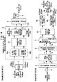
- Fig. 1 is a diagram showing a communication device according to a first embodiment of the present invention.
- description will be made on a case where transmission data is divided in two polarized waves (an X polarized wave, a Y polarized wave) and transmitted.
- a transmission device data is distributed to the two X and Y polarized waves by a distributor 1, and coding for error correction is performed for each by a transmit digital signal processing portion 2.
- the coding differs according to a method for error correction.
- Each piece of coded transmission data is transferred to an optical fiber 4 via an optical modulator 3. Note that various kinds of digital signal processing are performed for the pieces of transmission data before being coded.
- received data is separated into received data of the X polarized wave and received data of the Y polarized wave by an optical demodulator 5 and sent to a digital signal processing portion 6.
- the received data of the X polarized wave is indicated by coordinate data (Xi, Xq) on signal space
- the received data of the Y polarized wave is indicated by coordinate data (Yi, Yq) on the signal space.
- the digital signal processing portion 6 compensates chromatic dispersion, polarization dispersion, and frequency/phase fluctuation that have occurred during transmission, by digital signal processing. For each polarized wave, the compensated received data is supplied to a determination portion 7, and a determination is performed from coordinate data to digital data. In this case, the digital data is calculated in a format depending on a method for error correction to be connected next. For example, there may be a case where likelihood information showing certainty of the data is added.
- the digital data from the determination portion 7 (including the likelihood information depending on cases) is supplied to first and second error correction circuits 8a, 8b, and error correction is performed. Accordingly, an error rate characteristic is improved.
- an integrating portion 9 integrates the data on the X polarized wave side and the data on the Y polarized wave side.
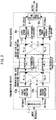
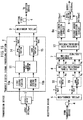
- Fig. 2 is a diagram showing an error correction device used for the communication device according to the first embodiment of the present invention. Only portion related to the error correction device is extracted from the communication device of Fig. 1 . First and second coding portions 10a, 10b and a transmission side combining portion 11 are included in the transmit digital signal processing portion 2 of Fig. 1 . A reception side combining portion 12 is included in the digital signal processing portion 6 of Fig. 1 . The first and second coding portions 10a, 10b and the first and second error correction circuits 8a, 8b configure FEC (Feedforward Error Correction).
- FEC eedforward Error Correction
- Transmission lines I, II are a plurality of transmission lines configured in one carrier such as light from one optical fiber or one laser and integrally indicate the transmission device, a transmission medium, and the reception device.
- QPSK Quadrature Phase Shift Keying
- 16QAM Quadrature Amplitude Modulation
- transmission by QPSK is indicated by the transmission line I
- transmission by 16QAM is indicated by the transmission line II.
- the present invention is not limited to an optical carrier but is applicable to all communications including optical communication. Therefore, one carrier can be referred to as one channel band. Further, in the case of transmitting the plurality of transmission lines I, II by different carriers, the present invention can be also applied.
- the first and second coding portions 10a, 10b on the transmission side perform certain coding processing for a series of bit data with a certain length (a coding length) out of the pieces of transmission data and output the bit data as code words.
- This coding processing differs according to error correction methods, the coding processing being giving a predetermined rule to the data itself, adding related bits obtained from the data, or the like.
- the processing may be performed for each predetermined data length or may be continuously performed.
- the first and second error correction circuits 8a, 8b on the reception side detect bits estimated to be erroneous, from the coded data (the code words) and correct the bits.
- the error correction is performed for each coding length (code word), and there may be a case where the coding length is hundreds of bytes to thousands of bytes.
- the first and second coding portions 10a, 10b and the transmission lines I, II are combined by the transmission side combining portion 11 according to a set ratio.
- the transmission line I, II and the first and second error correction circuits 8a, 8b are combined by the reception side combining portion 12 according to a set ratio.
- the combination is not one-to-one combination but plurality-to-plurality combination.
- Each of the code words coded by the first and second coding portions 10a, 10b is assigned to any of the plurality of transmission line I, II. However, one code word may be divided and assigned to the plurality of transmission lines I, II.
- the term "assign" also includes the meaning of the term "allocate”.
- the transmission line I is a transmission line having a high transmission characteristic that is relatively invulnerable to noise
- the transmission line II is a transmission line having a low transmission characteristic that is more vulnerable to noise than the transmission line I.
- the transmission line I is a transmission line by QPSK
- the transmission line II is a transmission line by 16QAM
- the transmission line I is better than the transmission line II in the transmission characteristic.
- the first error correction circuit 8a though the error correction capability is relatively high, the circuit scale and power consumption are large.
- the second error correction circuit 8b though the error correction capability is lower than the first error correction circuit 8a, the circuit scale and power consumption are small.
- the first error correction circuit 8a performs error correction by LDPC (Low Density Parity Check) codes
- the second error correction circuit 8b performs error correction by Reed-Solomon codes.
- LDPC codes have a higher error correction capability than Reed-Solomon codes, and the circuit scale and power consumption are larger.
- the characteristic difference described above can be configured according to a code length and the like. Note that the error correction method is not limited to the method described above, and other error correction methods such as convolutional coding and Viterbi decoding are also possible.
- Fig. 3 is a diagram showing correction operations of the first and second error correction circuits.
- a horizontal axis indicates an error rate BERin before error correction is performed, and a vertical axis indicates an error rate BERout after error correction is performed.
- the BER (Bit Error Rate) is an error rate for each bit.
- An error correction effect is shown by the error rate BERout of output decreasing more than the error rate BERin of input.
- an error rate BERout_A of output of the first error correction circuit 8a is smaller than an error rate BERout_B of output of the second error correction circuit 8b. This shows that the first error correction circuit 8a has a higher error correction capability than the second error correction circuit 8b.
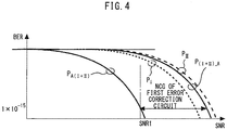
- Figs. 4 and 5 are diagrams showing error rate characteristics of the error correction device of the present invention.
- an error rate characteristic P I of the transmission line I and an error rate characteristic P II of the transmission line II are common.
- Fig. 4 further shows an overall transmission line error rate characteristic P(I+II) _ A (before error correction) of the transmission lines I, II to be combined with the first error correction circuit 8a, and an error rate characteristic P A(I+II) (after error correction) when the transmission lines I, II are combined with the first error correction circuit 8a.
- Fig. 4 is diagrams showing error rate characteristics of the error correction device of the present invention.
- an error rate characteristic P I of the transmission line I and an error rate characteristic P II of the transmission line II are common.
- Fig. 4 further shows an overall transmission line error rate characteristic P(I+II) _ A (before error correction) of the transmission lines I, II to be combined with the first error correction circuit 8a, and an error rate characteristic P A(I+II) (after error correction
- FIG. 5 further shows an overall transmission line error rate characteristic P (I+II)_B (before error correction) of the transmission lines I, II to be combined with the second error correction circuit 8b, and an error rate characteristic P B(I+II) (after error correction) when the transmission lines I, II are combined with the second error correction circuit 8b.
- SNR is a signal-to-noise ratio. For example, if the transmission line I is for transmission by QPSK, and the transmission line II is for transmission by 16QAM, then the error rate characteristic P I of the transmission line I is better than the error rate characteristic P II of the transmission line II.
- Figs. 4 and 5 are image diagrams and may be different from actual error rate characteristics.
- Fig. 3 a state in which the error rate itself is improved by FEC_A is shown.
- the error rate characteristic P A(I+II) for an input SNR becomes a curve drawn by a solid line on a left side of Fig. 4 .
- the overall transmission line error rate characteristic P (I+II)_A before error correction is performed is a curve drawn by a solid line on a right side of Fig. 4 .
- a difference between input SNRs for the same error rate shows the error correction capability of the first error correction circuit 8a. In general, this is an indicator showing an error correction capability, which is referred to as NCG (Net Coding Gain).
- the transmission side combining portion 11 and the reception side combining portion 12 perform similar operations in synchronization with each other. That is, the transmission side combining portion 11 distributes output data of the first coding portion 10a to the transmission line I and the transmission line II and distributes output data of the second coding portion 10b to the transmission line I and the transmission line II.
- the reception side combining portion 12 combines the data from the first coding portion 10a distributed to the transmission line I and the transmission line II with the first error correction circuit 8a and combines the data from the second coding portion 10b distributed to the transmission line I and the transmission line II with the second error correction circuit 8b.
- the transmission side combining portion 11 can not only distribute the code words in units of coding (that is, for each code word) but also distribute data in the code words to the transmission lines I, II.
- This distribution can be performed in units of several bits. Accordingly, even when a coding length is long or when continuous coding is performed, combination with the plurality of transmission lines easily becomes possible, and precise adjustment of a ratio of distribution becomes possible. Note that, in the case of distributing data in coding, calculation of an overall error rate is nonlinear and complicated. A method for the calculation will be shown in description of an operation below.
- Input data of an overall data rate R0 [Gbps] is distributed as R1 [Gbps] data to be supplied to the first coding portion 10a and R2 [Gbps] data to be supplied to the second coding portion 10b.
- a ratio of this distribution is a part of an algorithm for a method for subsequent combination by the transmission side combining portion 11.
- Each of the pieces of data coded by the first and second coding portions 10a, 10b are supplied to the transmission side combining portion 11.
- an information amount of data may change by coding, it is indicated by the same transmission rate here for simplification of description.
- the transmission side combining portion 11 supplies data of R I_A [Gbps] out of the data of R1 [Gbps] to the transmission line I and supplies remaining data of R II_A [Gbps] to the transmission line II. Furthermore, the transmission side combining portion 11 supplies data of R I_B [Gbps] out of the data of R2 [Gbps] to the transmission line I and supplies remaining data of R II_B [Gbps] to the transmission line II.
- each of the pieces of data transmitted through the transmission line I and the transmission line II is supplied to the reception side combining portion 12.
- the reception side combining portion 12 combines the data of R I_A [Gbps] with the first error correction circuit 8a out of the data from the transmission line I and combines the remaining data of R I_B [Gbps] with the second error correction circuit 8b. Furthermore, the reception side combining portion 12 combines the data of R II_A [Gbps] with the first error correction circuit 8a out of the data from the transmission line II and combines the remaining data of R II_B [Gbps] with the second error correction circuit 8b.
- the integrating portion 9 integrates these and outputs data of R0 [Gbps].
- an overall error characteristic P T of the whole system is determined by the following formula from the error rate characteristic P A(I+II) in a case where the first error correction circuit 8a is combined with the plurality of transmission lines I, II, the error rate characteristic P B(I+II) in a case where the second error correction circuit 8b is combined with the plurality of transmission lines I, II, and distribution rates R1/R0 and R2/R0 thereof.
- R0 R1+R2
- R1 R I_A +R II_A
- a method of distributing data in the combining portion will be described below.
- power consumption of the whole device can be reduced by using the low-power second error correction circuits 8b more often.
- data transmitted through the transmission line I with a high transmission characteristic is combined with the second error correction circuit 8b with a relatively low error correction capability.
- data transmitted through the transmission line II with a low transmission characteristic is combined with the first error correction circuit 8a with a high error correction capability.
- optimization design becomes easy.
- the design becomes further easier. Though adjustment of transmission power is not especially mentioned below, adjustment of transmission power is also included in design.
- Table 1 shows an example in which input data 120 [Gbps] is assigned according to the above policy.
- Table 1 shows a transmission rate for each of a case where the transmission line I and the first error correction circuit 8a are combined, a case where the transmission line I and the second error correction circuit 8b are combined, a case where the transmission line II and the first error correction circuit 8a are combined, and a case where the transmission line II and the second error correction circuit 8b are combined.
- Rate [Gbps] First error correction circuit Second error correction circuit Subtotal Transmission line I R I_A :0 R I_B :60 60 Transmission line II R II_A :40 R II_B :20 60 Total R1:40 R2:80 R0:120
- P T 40 120 ⁇ FEC _ A 0 40 P I + 40 40 P II + 80 120 ⁇ FEC _ B 60 80 P I + 20 80 P II
- a method for combining a plurality of transmission lines and a plurality of error correction circuits that is, a method for distributing data is decided in consideration of the overall error rate P T and total power. Specifically, an allowable value for an error rate in the case of combining all with the first error correction circuit 8a with a high error correction capability is determined, and the rate of combination with the low-power second error correction circuits 8b is increased so that the overall error rate P T is within the allowable value.
- the transmission line I with a high transmission characteristic is combined with the second error correction circuit 8b with a low correction capability and low power consumption at a ratio larger than that of the first error correction circuit 8a, and the transmission line II with a low transmission characteristic is combined with the first error correction circuit 8a with a high correction capability and high power consumption at a ratio larger than that of the second error correction circuit 8b. Accordingly, it is possible to improve overall transmission characteristics while suppressing power consumption.
- a plurality of transmission lines corresponding to a plurality of modulation schemes or a plurality of transmission characteristics are configured, respectively.
- a plurality of transmission lines are configured in one carrier or one channel band.
- one channel band is synonymous with one carrier (carrier wave).
- the plurality of subcarriers of OFDM are transmitted by one carrier, and, therefore, a bundle of the plurality of subcarriers is regarded as one carrier or one channel.
- one code word which is a series of outputs coded by FEC is assigned to a plurality of transmission lines. For example, one code word is assigned to the transmission line I and the transmission line II. There is a method in which each code word is assigned to a separate transmission line (for example, a first code word is assigned to the transmission line I, and a second code word is assigned to the transmission line II).
- a first code word is assigned to the transmission line I
- a second code word is assigned to the transmission line II.
- Fig. 6 is a diagram showing an example of transmission lines.
- the plurality of transmission lines are configured in one carrier or one channel band.
- Example 1 shows a method of, by utilizing that a high-order bit and a low-order bit among multi-leveled bits are different in the transmission characteristic, configuring them as a plurality of transmission lines.
- a high-order bit and a low-order bit among multi-leveled bits are different in the transmission characteristic, configuring them as a plurality of transmission lines.
- Examples 2 to 4 show methods in which a plurality of modulation schemes (for example, QPSK modulation and 16QAM modulation) are configured as a plurality of transmission lines.
- the QPSK modulation is relatively more invulnerable to the 16QAM modulation to noise.
- the modulation scheme is changed for each OFDM subcarrier.
- the modulation scheme is changed in time division.
- the modulation scheme is changed for each polarized wave. Description will be made on these examples of transmission lines in detail in the second to sixth embodiments below.
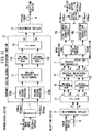
- Fig. 7 is a diagram showing a communication device according to a second embodiment of the present invention.
- the present embodiment is a communication device applied to coherent optical communication.
- coherent optical communication is configured with transmissions by the X polarized wave and the Y polarized wave. Since a transmission configuration by the Y polarized wave is similar to a transmission configuration of the X polarized wave, only the transmission by the X polarized wave is shown here, and the transmission configuration by the Y polarized wave is omitted.
- a transmission device After input data is coded by the first and second coding portions 10a, 10b and is combined with a plurality of transmission lines by the transmission side combining portion 11.
- the data combined with the plurality of transmission lines is multi-leveledly modulated by a mapping circuit 13 and output from the optical modulator 3 as an optical signal. Note that though a series of digital signal processing is generally performed in the transmission device, it is omitted here.
- the digital signal processing portion 6 performs digital signal processing.
- the determination portion 7 converts the output from coordinate data to bit data and divides the bit data into pieces of data for a plurality of transmission lines. The pieces of data are combined with the first and second error correction circuits 8a, 8b via the reception side combining portion 12.
- the present embodiment two transmission lines and two FECs are combined to transmit data.
- the FECs the high-power first error correction circuit 8a with a high performance and the low-power second error correction circuit 8b with a conventional performance are used.
- the present embodiment by utilizing that a high-order bit and a low-order bit among multi-leveled bits are different in the transmission characteristic, they are configured as a plurality of transmission lines. A method therefor will be described below.
- Figs. 8 to 10 are diagrams showing an example of signal mapping of 16QAM used in the second embodiment of the present invention.
- the mapping shown here is an example, and mapping is not limited thereto.
- 16QAM for input data, sixteen signal points are assigned for every four bits (b0, b1, b2, b3).
- (b0, b1) are defined as high-order bits
- (b2, b3) are defined as low-order bits.
- Fig. 9 is a diagram displaying only the high-order bits (b0, b1)
- Fig. 10 is a diagram displaying only the low-order bits (b2, b3).
- the transmission line I is configured with transmission by the high-order bits
- the transmission line II is configured with transmission by the low-order bits.
- the transmission side combining portion 11 distributes data from the first and second coding portions 10a, 10b to the high-order bits (b0, b1) and the low-order bits (b2, b3) to supply the data to the mapping circuit 13.
- the reception side combining portion 12 assigns the high-order bits (b0, b1) and the low-order bits (b2, b3) of the data from the determination portion 7, to the first and second error correction circuits 8a, 8b in a method opposite to the method of the transmission side combining portion 11.
- high-order bit transmission as the transmission line I and low-order bit transmission as the transmission line II can be freely combined with the first and second error correction circuits 8a, 8b.
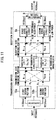
- Fig. 11 is a diagram illustrating an operating principle of the communication device according to the second embodiment of the present invention. An example of assignment at this time will be described below.
- Each of the pieces of data coded by the first coding portion 10a and the second coding portion 10b is supplied to the transmission side combining portion 11.
- a data amount may increase.
- the data amount is the same as the input data for simplification of description.
- the transmission side combining portion 11 assigns all the output of 40 Gbps of the first coding portion 10a to the low-order bits (b2, b3) of mapping. Accordingly, the output 40 Gbps of the first coding portion 10a is combined with the transmission line I of the low-order bits. In this example, there is no assignment from the output of the first coding portion 10a to the high-order bits (b0, b1).
- the high-order bits (b0, b1) of 60 Gbps and the low-order bits (b2, b3) of 60 Gbps are supplied to the reception side combining portion 12. At this time, likelihood information is added depending on error correction methods.
- the reception side combining portion 12 supplies all the data of the high-order bits of 60 Gbps to the second error correction circuit 8b. Further, out of the low-order bits of 60 Gbps, the data of 40 Gbps is supplied to the first error correction circuit 8a, and the data of 20 Gbps is supplied to the second error correction circuit 8b.
- the data of 80 Gbps is assigned to the low-power second error correction circuit 8b, and the data of 40 Gbps is assigned to the high-power first error correction circuit 8a. Therefore, in comparison with the case where all the data is assigned to the high-power first error correction circuit 8a, drastic power consumption reduction can be achieved.
- the overall error rate P T can be calculated similarly to the first embodiment. Since the rate at which the transmission line II with a relatively low transmission characteristic is combined with the first error correction circuit 8a with a high error correction capability is increased, the overall error rate falls within an acceptable range. Accordingly, it is possible to improve overall transmission characteristics while suppressing power consumption.
- Fig. 12 is a diagram showing a communication device according to a third embodiment of the present invention.
- the modulation scheme is changed to 64QAM.
- Other components are similar to components of the second embodiment.
- (b0, b1) are defined as high-order bits
- (b2, b3) are defined as middle-order bits
- (b4, b5) are defined as low-order bits.
- high-order bit transmission, middle-order bit transmission, and low-order bit transmission higher-order bit transmission has a better transmission characteristic
- the transmission line I, the transmission line II, and a transmission line III are respectively configured by high-order bit transmission, middle-order bit transmission, and low-order bit transmission, as in the case of 16QAM.
- FEC coded data supplied from the transmission side combining portion 11 to the mapping circuit 13 is assigned to the three kinds of transmission bits (the high-order bits, the middle-order bits, and the low-order bits).
- the data supplied from the determination portion 7 to the reception side combining portion 12 on the reception side is also assigned in an opposite direction at the same rate as the transmission side. An example of the assignment will be described below.
- the overall error rate can be determined similarly to the case of 16QAM.
- Fig. 13 is a diagram showing a communication device according to a fourth embodiment of the present invention.
- the method for configuring the plurality of transmission lines is changed from the method of utilizing multi-leveled bits of the second embodiment to a method of switching a modulation scheme for each subcarrier of OFDM.
- Data combined with the plurality of transmission lines by the transmission side combining portion 11 is modulated by a QPSK modulating portion 14 and a 16QAM modulating portion 15, and the data passes through an OFDM 16 and is output from the optical modulator 3 as an optical signal.
- an output signal of the optical demodulator 5 passes through an OFDM 17 and is demodulated by a QPSK demodulating portion 18 and a 16QAM demodulation portion 19.
- input data is generally transmitted being divided for a plurality of subcarriers.
- a plurality of transmission lines with different transmission characteristics can be configured.
- QPSK-modulated data and 16QAM-modulated data can be transmitted by separate subcarriers.
- QPSK modulation has a higher transmission characteristic than 16QAM modulation. Therefore, transmission by QPSK modulation corresponds to the transmission line I of the first embodiment, and transmission by 16QAM corresponds to the transmission line II.
- a method for combining the first error correction circuit 8a with a high error correction capability and power consumption and the second error correction circuit 8b with a relatively low error correction capability and power consumption with the transmission line I and the transmission line II can be decided similarly to the first embodiment.
- An example of a method for the combination is shown below.
- An optimal combination method in the system is decided from the overall error rate and power consumption as described above.
- more transmission lines can be configured by using other modulation schemes (for example, BPSK (Binary Phase Shift Keying) or 64QAM). Further, since the number of subcarriers to be assigned can be arbitrarily changed, it is not necessary to cause the data rates of the transmission line I and the transmission line II to be the same.
- BPSK Binary Phase Shift Keying
- 64QAM 64QAM
- Fig. 14 is a diagram showing a communication device according to a fifth embodiment of the present invention.
- the method for configuring the plurality of transmission lines is changed from the method of switching a modulation scheme for each subcarrier of OFDM of the fourth embodiment to a method of switching among modulation schemes in time division.
- Data combined with the plurality of transmission lines by the transmission side combining portion 11 passes through a QPSK/16QAM time-division switching portion 20 and is output from the optical modulator 3 as an optical signal.
- an output signal of the optical demodulator 5 passes through a QPSK/16QAM time-division switching portion 21 and is input to the digital signal processing portion 6.
- data can be transmitted by a plurality of modulation schemes with different transmission characteristics in the frames or for each frame.
- a modulation scheme can be switched for each symbol or for every several symbols.
- QPSK modulation and 16QAM modulation can be switched.
- QPSK modulation has a higher transmission characteristic than 16QAM modulation. Therefore, transmission by QPSK modulation corresponds to the transmission line I of the first embodiment, and transmission by 16QAM corresponds to the transmission line II.
- transmission is performed in time division.
- a method for combining the first error correction circuit 8a with a high error correction capability and power consumption and the second error correction circuit 8b with a relatively low error correction capability and power consumption with the transmission line I and the transmission line II can be decided similarly to the first embodiment.
- An example of a method for the combination is shown below.
- An optimal combination method in the system is decided from the overall error rate and power as described above.
- more transmission lines can be configured by using other modulation schemes (for example, BPSK or 64QAM). Further, it is not necessary to cause the data rates of the transmission line I and the transmission line II to be the same depending on assigned time. Furthermore, by changing transmission power and SNR for each modulation scheme, that is, for each transmission line, it becomes easy to perform optimization of the overall error rate.
- modulation schemes for example, BPSK or 64QAM
- Fig. 15 is a diagram showing a communication device according to a sixth embodiment of the present invention.
- the method for configuring the plurality of transmission lines is changed from the method of switching the modulation scheme for each subcarrier of OFDM of the fourth embodiment to a method of switching a modulation scheme for each polarized wave. That is, the X polarized wave is transmitted by QPSK modulation, and the Y polarized wave is transmitted by 16QAM modulation.
- QPSK modulation has a higher transmission characteristic than 16QAM modulation. Therefore, transmission by QPSK modulation corresponds to the transmission line I of the first embodiment, and transmission by 16QAM corresponds to the transmission line II.
- description has been made using only the X polarized wave in the third and fourth embodiments a method of configuring the plurality of transmission lines using both of the X polarized wave and the Y polarized wave will be described in the present embodiment.
- a method for combining the first error correction circuit 8a with a high error correction capability and power consumption and the second error correction circuit 8b with a relatively low error correction capability and power consumption with the transmission line I and the transmission line II can be decided similarly to the first embodiment.
- An example of a method for the combination is shown below.
- An optimal combination method in the system is decided from the overall error rate and power as described above. Note that, in the case of configuring the plurality of transmission lines with polarized waves, by changing transmission power and SNR for each modulation scheme, that is, for each transmission line, it becomes easy to perform optimization of the overall error rate.
- QPSK and 16QAM are illustrated as the plurality of modulation schemes in the third to fifth embodiments, the modulation schemes are not limited thereto, but all modulation schemes are applicable. As other modulation schemes, BPSK, 8QAM, 64QAM, 256QAM, and the like are also applicable.
- first to fifth embodiments may be mutually combined.
- the method of using multi-leveled bits in the first and second embodiments and the method of performing transmission in time division of the third embodiment can be combined. By such a combination, it is possible to further optimize an error rate.
- a program for implementing the error correction methods according to the first to fifth embodiments may be recorded in a computer-readable recording medium so that the program recorded in the recording medium is read in and executed by a computer system or a programmable logic device to perform phase compensation.
- the "computer system” described here may contain hardware such as OS, peripheral equipment, etc.
- the "computer system” may contain a WWW system having a homepage providing environment (or displaying environment).
- the "computer-readable recording medium” may be a portable medium such as a flexible disc, a magneto-optic disc, ROM and CD-ROM, or a storage device such as a hard disc incorporated in a computer system.
- the "computer-readable recording medium” may contain an element for holding a program for a constant time like a volatile memory (RAM) in a computer system serving as a server or a client when a program is transmitted through a network such as the Internet or a communication line such as a telephone line.
- the program may be transmitted from a computer system having a storage device or the like in which the program is stored, to another computer system via a transmission medium or by transmission waves in a transmission medium.
- the "transmission medium” for transmitting the program is a medium having a function of transmitting information like a network (communication network) such as the Internet or a communication circuit (communication line) such as a telephone line or the like.
- the program may be provided to perform a part of the foregoing function.
- the program may be provided to perform the foregoing function in combination with a program which has been already stored in the computer system, so-called a differential file (differentia program).
Landscapes
- Engineering & Computer Science (AREA)
- Signal Processing (AREA)
- Computer Networks & Wireless Communication (AREA)
- Physics & Mathematics (AREA)
- Probability & Statistics with Applications (AREA)
- Theoretical Computer Science (AREA)
- Electromagnetism (AREA)
- Environmental & Geological Engineering (AREA)
- Multimedia (AREA)
- Optics & Photonics (AREA)
- Detection And Prevention Of Errors In Transmission (AREA)
- Error Detection And Correction (AREA)
Abstract
Description
- The present invention relates to an error correction device, an error correction method, and a communication device, which can improve overall transmission characteristics while suppressing power consumption.
- In coherent optical communication, for improvement of transmission characteristics, distortion, and frequency/phase fluctuation that occur during transmission are compensated by digital signal processing. For further improvement of the transmission characteristics, an error correction circuit is provided between transmission and reception in addition to the above compensation function so that data errors in the transmission characteristics are reduced (for example, see NPL 1). In general, coding for error correction is performed for data on a transmission side, and error correction is performed on a reception side according to the coding.
- Summary Report "R&D on the Digital Coherent Signal Processing Technology for Large-capacity Optical Communication Networks"; Senichi Suzuki et al.; The Journal of the Institute of Electronics, Information and Communication Engineers, Vol. 95, No. 12, 2012, pp. 1100-1116
- However, in a conventional communication device, in order to improve overall transmission characteristics, it is necessary not only to improve transmission characteristics between modulation and demodulation but also to use an error correction circuit with a high error correction capability to further reduce errors of reproduced data itself. However, as for the error correction circuit with a high error correction capability, a circuit scale is generally large, and power consumption is also large. Therefore, a communication device with a high error correction capability has a problem that power consumption is large.
- The present invention has been made to solve the problem as described above, and its object is to obtain an error correction device, an error correction method, and a communication device, which can improve overall transmission characteristics while suppressing power consumption.
- An error correction device according to the present invention used in a communication device transmitting data of a predetermined transmission rate through a plurality of transmission lines configured in one carrier or one channel band, includes: a plurality of error correction circuits correcting errors of the data transmitted through the plurality of transmission lines; and a combining portion combining the plurality of transmission lines to the plurality of error correction circuits, the plurality of transmission lines includes a first transmission line, and a second transmission line having a lower transmission characteristic than the first transmission line, wherein the plurality of error correction circuits include a first error correction circuit, and a second error correction circuit having lower error correction capability and power consumption than the first error correction circuit, and the combining portion uses a function of redundantly combining a plurality of error correction circuits in one transmission line, combines the first transmission line with the second error correction circuit at a higher rate than the first error correction circuit, and combines the second transmission line with the first error correction circuit at a higher rate than the second error correction circuit.
- The present invention makes it possible to improve overall transmission characteristics while suppressing power consumption.
-
-
Fig. 1 is a diagram showing a communication device according to a first embodiment of the present invention. -
Fig. 2 is a diagram showing an error correction device used for the communication device according to the first embodiment of the present invention. -
Fig. 3 is a diagram showing correction operations of the first and second error correction circuits. -
Fig. 4 is a diagram showing error rate characteristics of the error correction device of the present invention. -
Fig. 5 is a diagram showing error rate characteristics of the error correction device of the present invention. -
Fig. 6 is a diagram showing an example of transmission lines. -
Fig. 7 is a diagram showing a communication device according to a second embodiment of the present invention. -
Fig. 8 is a diagram showing an example of signal mapping of 16QAM used in the second embodiment of the present invention. -
Fig. 9 is a diagram showing an example of signal mapping of 16QAM used in the second embodiment of the present invention. -
Fig. 10 is a diagram showing an example of signal mapping of 16QAM used in the second embodiment of the present invention. -
Fig. 11 is a diagram illustrating an operating principle of the communication device according to the second embodiment of the present invention. -
Fig. 12 is a diagram showing a communication device according to a third embodiment of the present invention. -
Fig. 13 is a diagram showing a communication device according to a fourth embodiment of the present invention. -
Fig. 14 is a diagram showing a communication device according to a fifth embodiment of the present invention. -
Fig. 15 is a diagram showing a communication device according to a sixth embodiment of the present invention. - An error correction device, an error correction method, and a communication device according to the embodiments of the present invention will be described with reference to the drawings. The same components will be denoted by the same symbols, and the repeated description thereof may be omitted.
-
Fig. 1 is a diagram showing a communication device according to a first embodiment of the present invention. Here, description will be made on a case where transmission data is divided in two polarized waves (an X polarized wave, a Y polarized wave) and transmitted. - In a transmission device, data is distributed to the two X and Y polarized waves by a
distributor 1, and coding for error correction is performed for each by a transmit digitalsignal processing portion 2. The coding differs according to a method for error correction. Each piece of coded transmission data is transferred to anoptical fiber 4 via anoptical modulator 3. Note that various kinds of digital signal processing are performed for the pieces of transmission data before being coded. - In a reception device, received data is separated into received data of the X polarized wave and received data of the Y polarized wave by an
optical demodulator 5 and sent to a digitalsignal processing portion 6. Here, the received data of the X polarized wave is indicated by coordinate data (Xi, Xq) on signal space, and the received data of the Y polarized wave is indicated by coordinate data (Yi, Yq) on the signal space. - The digital
signal processing portion 6 compensates chromatic dispersion, polarization dispersion, and frequency/phase fluctuation that have occurred during transmission, by digital signal processing. For each polarized wave, the compensated received data is supplied to adetermination portion 7, and a determination is performed from coordinate data to digital data. In this case, the digital data is calculated in a format depending on a method for error correction to be connected next. For example, there may be a case where likelihood information showing certainty of the data is added. - The digital data from the determination portion 7 (including the likelihood information depending on cases) is supplied to first and second
error correction circuits integrating portion 9 integrates the data on the X polarized wave side and the data on the Y polarized wave side. -
Fig. 2 is a diagram showing an error correction device used for the communication device according to the first embodiment of the present invention. Only portion related to the error correction device is extracted from the communication device ofFig. 1 . First andsecond coding portions side combining portion 11 are included in the transmit digitalsignal processing portion 2 ofFig. 1 . A receptionside combining portion 12 is included in the digitalsignal processing portion 6 ofFig. 1 . The first andsecond coding portions error correction circuits - In this description, the term "combine" also includes the meaning of "connect" and "couple".
- Transmission lines I, II are a plurality of transmission lines configured in one carrier such as light from one optical fiber or one laser and integrally indicate the transmission device, a transmission medium, and the reception device. For example, in a case where QPSK (Quadrature Phase Shift Keying) modulated data and 16QAM (Quadrature Amplitude Modulation) modulated data are transmitted on one optical carrier, transmission by QPSK is indicated by the transmission line I, and transmission by 16QAM is indicated by the transmission line II. Note that the present invention is not limited to an optical carrier but is applicable to all communications including optical communication. Therefore, one carrier can be referred to as one channel band. Further, in the case of transmitting the plurality of transmission lines I, II by different carriers, the present invention can be also applied.
- In this description, the term "line" also includes the meaning of "path".
- The first and
second coding portions - The first and second
error correction circuits - The first and
second coding portions side combining portion 11 according to a set ratio. The transmission line I, II and the first and seconderror correction circuits side combining portion 12 according to a set ratio. In this case, the combination is not one-to-one combination but plurality-to-plurality combination. Each of the code words coded by the first andsecond coding portions - Here, the transmission line I is a transmission line having a high transmission characteristic that is relatively invulnerable to noise, and the transmission line II is a transmission line having a low transmission characteristic that is more vulnerable to noise than the transmission line I. For example, if the transmission line I is a transmission line by QPSK, and the transmission line II is a transmission line by 16QAM, then the transmission line I is better than the transmission line II in the transmission characteristic.
- Further, as for the first
error correction circuit 8a, though the error correction capability is relatively high, the circuit scale and power consumption are large. As for the seconderror correction circuit 8b, though the error correction capability is lower than the firsterror correction circuit 8a, the circuit scale and power consumption are small. For example, the firsterror correction circuit 8a performs error correction by LDPC (Low Density Parity Check) codes, and the seconderror correction circuit 8b performs error correction by Reed-Solomon codes. In general, LDPC codes have a higher error correction capability than Reed-Solomon codes, and the circuit scale and power consumption are larger. Of course, in the same error correction method, the characteristic difference described above can be configured according to a code length and the like. Note that the error correction method is not limited to the method described above, and other error correction methods such as convolutional coding and Viterbi decoding are also possible. -
Fig. 3 is a diagram showing correction operations of the first and second error correction circuits. A horizontal axis indicates an error rate BERin before error correction is performed, and a vertical axis indicates an error rate BERout after error correction is performed. The BER (Bit Error Rate) is an error rate for each bit. An error correction operation FEC_A [BERin] by the firsterror correction circuit 8a and an error correction operation FEC_B [BERin] by the seconderror correction circuit 8b are indicated by the following formulas:

- An error correction effect is shown by the error rate BERout of output decreasing more than the error rate BERin of input. For an error rate BERin of the same input, an error rate BERout_A of output of the first
error correction circuit 8a is smaller than an error rate BERout_B of output of the seconderror correction circuit 8b. This shows that the firsterror correction circuit 8a has a higher error correction capability than the seconderror correction circuit 8b. -
Figs. 4 and5 are diagrams showing error rate characteristics of the error correction device of the present invention. InFigs. 4 and5 , an error rate characteristic PI of the transmission line I and an error rate characteristic PII of the transmission line II are common.Fig. 4 further shows an overall transmission line error rate characteristic P(I+II)_A (before error correction) of the transmission lines I, II to be combined with the firsterror correction circuit 8a, and an error rate characteristic PA(I+II) (after error correction) when the transmission lines I, II are combined with the firsterror correction circuit 8a.Fig. 5 further shows an overall transmission line error rate characteristic P(I+II)_B (before error correction) of the transmission lines I, II to be combined with the seconderror correction circuit 8b, and an error rate characteristic PB(I+II) (after error correction) when the transmission lines I, II are combined with the seconderror correction circuit 8b. SNR is a signal-to-noise ratio. For example, if the transmission line I is for transmission by QPSK, and the transmission line II is for transmission by 16QAM, then the error rate characteristic PI of the transmission line I is better than the error rate characteristic PII of the transmission line II. Note thatFigs. 4 and5 are image diagrams and may be different from actual error rate characteristics. - When it is assumed that, in the
distributor 1, out of a transmission rate R1 [Gbps] assigned to thefirst coding portion 10a, a transmission rate to be combined with the transmission line I is RI_A [Gbps], and a transmission rate to be combined with the transmission line II is remaining RII_A [Gbps], the overall transmission line error rate characteristic P(I+II)_A is shown by the following formula:
- Furthermore, if they are combined with the first
error correction circuit 8a, the error rate characteristic PA(I+II) is shown by the following formula:
- In
Fig. 3 , a state in which the error rate itself is improved by FEC_A is shown. The error rate characteristic PA(I+II) for an input SNR becomes a curve drawn by a solid line on a left side ofFig. 4 . Here, the overall transmission line error rate characteristic P(I+II)_A before error correction is performed is a curve drawn by a solid line on a right side ofFig. 4 . A difference between input SNRs for the same error rate shows the error correction capability of the firsterror correction circuit 8a. In general, this is an indicator showing an error correction capability, which is referred to as NCG (Net Coding Gain). - Similarly, when it is assumed that, in the
distributor 1, out of a transmission rate R2 [Gbps] assigned to thesecond coding portion 10b, a transmission rate to be combined with the transmission line I is RI_B [Gbps], and a transmission rate to be combined with the transmission line II is remaining RII_B [Gbps], the overall transmission line error rate characteristic P(I+II)_B is shown by the following formula:
- Furthermore, if they are combined with the second
error correction circuit 8b, the error rate characteristic PB(I+II) is shown by the following formula:
error correction circuit 8b is smaller than NCG of the firsterror correction circuit 8a. - The transmission
side combining portion 11 and the receptionside combining portion 12 perform similar operations in synchronization with each other. That is, the transmissionside combining portion 11 distributes output data of thefirst coding portion 10a to the transmission line I and the transmission line II and distributes output data of thesecond coding portion 10b to the transmission line I and the transmission line II. The receptionside combining portion 12 combines the data from thefirst coding portion 10a distributed to the transmission line I and the transmission line II with the firsterror correction circuit 8a and combines the data from thesecond coding portion 10b distributed to the transmission line I and the transmission line II with the seconderror correction circuit 8b. - Here, at the time of distributing code words which are output data of the
first coding portion 10a or thesecond coding portion 10b to the plurality of transmission lines I, II, the transmissionside combining portion 11 can not only distribute the code words in units of coding (that is, for each code word) but also distribute data in the code words to the transmission lines I, II. This distribution can be performed in units of several bits. Accordingly, even when a coding length is long or when continuous coding is performed, combination with the plurality of transmission lines easily becomes possible, and precise adjustment of a ratio of distribution becomes possible. Note that, in the case of distributing data in coding, calculation of an overall error rate is nonlinear and complicated. A method for the calculation will be shown in description of an operation below. - Next, a whole operation will be described. Input data of an overall data rate R0 [Gbps] is distributed as R1 [Gbps] data to be supplied to the
first coding portion 10a and R2 [Gbps] data to be supplied to thesecond coding portion 10b. A ratio of this distribution is a part of an algorithm for a method for subsequent combination by the transmissionside combining portion 11. Each of the pieces of data coded by the first andsecond coding portions side combining portion 11. Here, though, generally, an information amount of data may change by coding, it is indicated by the same transmission rate here for simplification of description. The transmissionside combining portion 11 supplies data of RI_A [Gbps] out of the data of R1 [Gbps] to the transmission line I and supplies remaining data of RII_A [Gbps] to the transmission line II. Furthermore, the transmissionside combining portion 11 supplies data of RI_B [Gbps] out of the data of R2 [Gbps] to the transmission line I and supplies remaining data of RII_B [Gbps] to the transmission line II. - Next, each of the pieces of data transmitted through the transmission line I and the transmission line II is supplied to the reception
side combining portion 12. The receptionside combining portion 12 combines the data of RI_A [Gbps] with the firsterror correction circuit 8a out of the data from the transmission line I and combines the remaining data of RI_B [Gbps] with the seconderror correction circuit 8b. Furthermore, the receptionside combining portion 12 combines the data of RII_A [Gbps] with the firsterror correction circuit 8a out of the data from the transmission line II and combines the remaining data of RII_B [Gbps] with the seconderror correction circuit 8b. - Lastly, the data of R1 [Gbps] reproduced by the first
error correction circuit 8a is output, and the data of R2 [Gbps] reproduced by the seconderror correction circuit 8b is output. The integratingportion 9 integrates these and outputs data of R0 [Gbps]. - Here, an overall error characteristic PT of the whole system is determined by the following formula from the error rate characteristic PA(I+II) in a case where the first
error correction circuit 8a is combined with the plurality of transmission lines I, II, the error rate characteristic PB(I+II) in a case where the seconderror correction circuit 8b is combined with the plurality of transmission lines I, II, and distribution rates R1/R0 and R2/R0 thereof. Here, R0=R1+R2, R1=RI_A+RII_A and R2=RI_B+RII_B are assumed. Note that the ratio of distribution is set for the receptionside combining portion 12 in advance.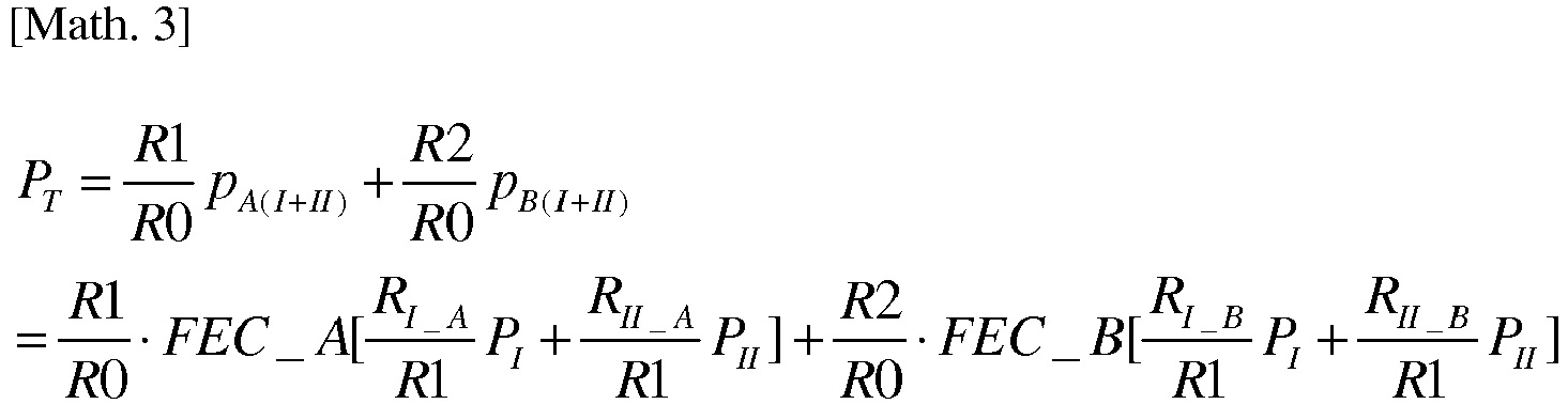
- A method of distributing data in the combining portion will be described below. At the time of distribution of data in the combining portion, power consumption of the whole device can be reduced by using the low-power second
error correction circuits 8b more often. However, it is desirable that data transmitted through the transmission line I with a high transmission characteristic is combined with the seconderror correction circuit 8b with a relatively low error correction capability. On the other hand, it is desirable that data transmitted through the transmission line II with a low transmission characteristic is combined with the firsterror correction circuit 8a with a high error correction capability. At this time, by performing adjustment so that the error rate characteristic PA(I+II) and the error rate characteristic PB(I+II) are almost the same characteristics as shown inFigs. 4 and5 , optimization design becomes easy. At this time, by adjusting transmission power together, the design becomes further easier. Though adjustment of transmission power is not especially mentioned below, adjustment of transmission power is also included in design. - Table 1 shows an example in which input data 120 [Gbps] is assigned according to the above policy. Table 1 shows a transmission rate for each of a case where the transmission line I and the first
error correction circuit 8a are combined, a case where the transmission line I and the seconderror correction circuit 8b are combined, a case where the transmission line II and the firsterror correction circuit 8a are combined, and a case where the transmission line II and the seconderror correction circuit 8b are combined.[Table 1] Rate [Gbps] First error correction circuit Second error correction circuit Subtotal Transmission line I RI_A:0 RI_B:60 60 Transmission line II RII_A:40 RII_B:20 60 Total R1:40 R2:80 R0:120 - The overall error rate PT at this time is indicated by the following formula:

- Note that a method for combining a plurality of transmission lines and a plurality of error correction circuits, that is, a method for distributing data is decided in consideration of the overall error rate PT and total power. Specifically, an allowable value for an error rate in the case of combining all with the first
error correction circuit 8a with a high error correction capability is determined, and the rate of combination with the low-power seconderror correction circuits 8b is increased so that the overall error rate PT is within the allowable value. - As described above, at the time of transmitting data, it is desirable to use a low-power error correction circuit with a conventional performance as far as possible for power consumption reduction. On the other hand, it is desirable to use a high-power error correction circuit with a high performance as far as possible for transmission characteristics improvement. Therefore, in the present embodiment, the transmission line I with a high transmission characteristic is combined with the second
error correction circuit 8b with a low correction capability and low power consumption at a ratio larger than that of the firsterror correction circuit 8a, and the transmission line II with a low transmission characteristic is combined with the firsterror correction circuit 8a with a high correction capability and high power consumption at a ratio larger than that of the seconderror correction circuit 8b. Accordingly, it is possible to improve overall transmission characteristics while suppressing power consumption. - Further, in general, in a plurality of carriers or a plurality of channel bands, a plurality of transmission lines corresponding to a plurality of modulation schemes or a plurality of transmission characteristics are configured, respectively. In the present embodiment, however, a plurality of transmission lines are configured in one carrier or one channel band. Note that one channel band is synonymous with one carrier (carrier wave). However, in a scheme in which a plurality of subcarriers are configured, like OFDM (Orthogonal Frequency Division Multiplexing), the plurality of subcarriers of OFDM are transmitted by one carrier, and, therefore, a bundle of the plurality of subcarriers is regarded as one carrier or one channel.
- Further, one code word which is a series of outputs coded by FEC is assigned to a plurality of transmission lines. For example, one code word is assigned to the transmission line I and the transmission line II. There is a method in which each code word is assigned to a separate transmission line (for example, a first code word is assigned to the transmission line I, and a second code word is assigned to the transmission line II). However, as a code length increases, there may be a case where precise adjustment of assignment cannot be performed.
-
Fig. 6 is a diagram showing an example of transmission lines. The plurality of transmission lines are configured in one carrier or one channel band. Example 1 shows a method of, by utilizing that a high-order bit and a low-order bit among multi-leveled bits are different in the transmission characteristic, configuring them as a plurality of transmission lines. For example, in 16QAM in which data is shown by four bits, the high order two bits are relatively more vulnerable to the low order two bits to noise. Examples 2 to 4 show methods in which a plurality of modulation schemes (for example, QPSK modulation and 16QAM modulation) are configured as a plurality of transmission lines. For example, between the QPSK modulation and the 16QAM modulation, the QPSK modulation is relatively more invulnerable to the 16QAM modulation to noise. In Example 2, the modulation scheme is changed for each OFDM subcarrier. In Example 3, the modulation scheme is changed in time division. In Example 4, the modulation scheme is changed for each polarized wave. Description will be made on these examples of transmission lines in detail in the second to sixth embodiments below. -
Fig. 7 is a diagram showing a communication device according to a second embodiment of the present invention. The present embodiment is a communication device applied to coherent optical communication. In general, coherent optical communication is configured with transmissions by the X polarized wave and the Y polarized wave. Since a transmission configuration by the Y polarized wave is similar to a transmission configuration of the X polarized wave, only the transmission by the X polarized wave is shown here, and the transmission configuration by the Y polarized wave is omitted. - In a transmission device, after input data is coded by the first and
second coding portions side combining portion 11. The data combined with the plurality of transmission lines is multi-leveledly modulated by amapping circuit 13 and output from theoptical modulator 3 as an optical signal. Note that though a series of digital signal processing is generally performed in the transmission device, it is omitted here. - In a reception device, after the
optical demodulator 5 converts the received signal from the optical signal to an electrical signal, the digitalsignal processing portion 6 performs digital signal processing. Thedetermination portion 7 converts the output from coordinate data to bit data and divides the bit data into pieces of data for a plurality of transmission lines. The pieces of data are combined with the first and seconderror correction circuits side combining portion 12. - ★ In the present embodiment, two transmission lines and two FECs are combined to transmit data. As the FECs, the high-power first
error correction circuit 8a with a high performance and the low-power seconderror correction circuit 8b with a conventional performance are used. Furthermore, in the present embodiment, by utilizing that a high-order bit and a low-order bit among multi-leveled bits are different in the transmission characteristic, they are configured as a plurality of transmission lines. A method therefor will be described below. -
Figs. 8 to 10 are diagrams showing an example of signal mapping of 16QAM used in the second embodiment of the present invention. However, the mapping shown here is an example, and mapping is not limited thereto. In 16QAM, for input data, sixteen signal points are assigned for every four bits (b0, b1, b2, b3). Here, (b0, b1) are defined as high-order bits, and (b2, b3) are defined as low-order bits.Fig. 9 is a diagram displaying only the high-order bits (b0, b1), andFig. 10 is a diagram displaying only the low-order bits (b2, b3). - When the high-order bits shown in
Fig. 9 are focused on, four signal points in each quadrant are indicated by the same values. For example, all of values of four signal points in the first quadrant are (0, 0). On the other hand, when the low-order bits shown inFig. 10 are focused on, four signal points in each quadrant are indicated by different values. For example, all of values of four signal points in the first quadrant are (1, 1), (0, 1), (1, 0) and (0, 0). In this case, an average distance between signal points with different values (e.x. (0,0) and (1,0)) in transmission by the high-order bits is larger than an average distance between signal points with different values (e.x. (0,0) and (1,0)) in transmission by the low-order bits. These distances are related to strength of resistance against noise that causes a data error. Therefore, it is seen that, in transmission by the high-order bits, the strength of resistance against noise is larger, and the transmission characteristic is better than in transmission by the low-order bits. - Utilizing this, the transmission line I is configured with transmission by the high-order bits, and the transmission line II is configured with transmission by the low-order bits. Specifically, the transmission
side combining portion 11 distributes data from the first andsecond coding portions mapping circuit 13. The receptionside combining portion 12 assigns the high-order bits (b0, b1) and the low-order bits (b2, b3) of the data from thedetermination portion 7, to the first and seconderror correction circuits side combining portion 11. By this method, high-order bit transmission as the transmission line I and low-order bit transmission as the transmission line II can be freely combined with the first and seconderror correction circuits -
Fig. 11 is a diagram illustrating an operating principle of the communication device according to the second embodiment of the present invention. An example of assignment at this time will be described below.[Table 2] Rate [Gbps] First error correction circuit Second error correction circuit Subtotal Transmission line I (b0, b1) RI_A:0 RI_B:60 60 Transmission line II (b2, b3) RII_A:40 RII_B:20 60 Total R1:40 R2:80 R0:120 - In the transmission device, by the
distributor 1, input data of an overall data rate 120 Gbps is distributed as R1=40 Gbps data to be supplied to thefirst coding portion 10a and R2=80 Gbps data to be supplied to thesecond coding portion 10b. Each of the pieces of data coded by thefirst coding portion 10a and thesecond coding portion 10b is supplied to the transmissionside combining portion 11. At this time, a data amount may increase. Here, however, it is assumed that the data amount is the same as the input data for simplification of description. - The transmission
side combining portion 11 assigns all the output of 40 Gbps of thefirst coding portion 10a to the low-order bits (b2, b3) of mapping. Accordingly, the output 40 Gbps of thefirst coding portion 10a is combined with the transmission line I of the low-order bits. In this example, there is no assignment from the output of thefirst coding portion 10a to the high-order bits (b0, b1). - On the other hand, out of the output of 80 Gbps of the
second coding portion 10b, data of 60 Gbps is assigned to the high-order bits (b0, b1) of mapping, and data of 20 Gbps is assigned to the low-order bits (b2, b3) of the mapping. After the mapping, both of high-order bit transmission and low-order bit transmission are 60 Gbps transmission, and transmission by 30 G symbol/s is performed. - In the reception device, the high-order bits (b0, b1) of 60 Gbps and the low-order bits (b2, b3) of 60 Gbps are supplied to the reception
side combining portion 12. At this time, likelihood information is added depending on error correction methods. The receptionside combining portion 12 supplies all the data of the high-order bits of 60 Gbps to the seconderror correction circuit 8b. Further, out of the low-order bits of 60 Gbps, the data of 40 Gbps is supplied to the firsterror correction circuit 8a, and the data of 20 Gbps is supplied to the seconderror correction circuit 8b. - By the process described above, out of the input data of the overall data rate 120 Gbps, the data of 80 Gbps is assigned to the low-power second
error correction circuit 8b, and the data of 40 Gbps is assigned to the high-power firsterror correction circuit 8a. Therefore, in comparison with the case where all the data is assigned to the high-power firsterror correction circuit 8a, drastic power consumption reduction can be achieved. - Further, the overall error rate PT can be calculated similarly to the first embodiment. Since the rate at which the transmission line II with a relatively low transmission characteristic is combined with the first
error correction circuit 8a with a high error correction capability is increased, the overall error rate falls within an acceptable range. Accordingly, it is possible to improve overall transmission characteristics while suppressing power consumption. -
Fig. 12 is a diagram showing a communication device according to a third embodiment of the present invention. In the present embodiment, in comparison with the communication device of 16QAM according to the second embodiment, the modulation scheme is changed to 64QAM. Other components are similar to components of the second embodiment. - In 64QAM modulation, sixty-four signal points are assigned for every six bits (b0, b1, b2, b3, b4, b5). Here, (b0, b1) are defined as high-order bits, (b2, b3) are defined as middle-order bits, and (b4, b5) are defined as low-order bits. Among high-order bit transmission, middle-order bit transmission, and low-order bit transmission, higher-order bit transmission has a better transmission characteristic, and the transmission line I, the transmission line II, and a transmission line III are respectively configured by high-order bit transmission, middle-order bit transmission, and low-order bit transmission, as in the case of 16QAM. Therefore, FEC coded data supplied from the transmission
side combining portion 11 to themapping circuit 13 is assigned to the three kinds of transmission bits (the high-order bits, the middle-order bits, and the low-order bits). The data supplied from thedetermination portion 7 to the receptionside combining portion 12 on the reception side is also assigned in an opposite direction at the same rate as the transmission side. An example of the assignment will be described below. In the present embodiment also, the overall error rate can be determined similarly to the case of 16QAM.[Table 3] Rate[Gbps] First error correction circuit Second error correction circuit Subtotal Transmission line I (b0, b1) RI_A:0 RI_B:40 40 Transmission line II (b2, b3) RII_A:10 RII_B:30 40 Transmission line III (b4, b5) RIII_A:30 RIII_B:10 40 Total R1:40 R2:80 R0:120 - In the present embodiment, out of input data of 120 Gbps, data of 80 Gbps is combined with the low-power second
error correction circuit 8b, and drastic power consumption reduction can be achieved in comparison with the case where all the data is assigned to the high-power firsterror correction circuit 8a. Since the rate of the transmission line III with a relatively low transmission characteristic is combined with the firsterror correction circuit 8a with a high error correction capability, the overall error rate is within an acceptable range. Accordingly, it is possible to improve overall transmission characteristics while suppressing power consumption. Further, in a case where the number of multi-leveled bits is large like 64QAM, precise combination adjustment becomes possible, and it is easy to perform optimization of combination. -
Fig. 13 is a diagram showing a communication device according to a fourth embodiment of the present invention. In the present embodiment, the method for configuring the plurality of transmission lines is changed from the method of utilizing multi-leveled bits of the second embodiment to a method of switching a modulation scheme for each subcarrier of OFDM. - Data combined with the plurality of transmission lines by the transmission
side combining portion 11 is modulated by aQPSK modulating portion 14 and a16QAM modulating portion 15, and the data passes through anOFDM 16 and is output from theoptical modulator 3 as an optical signal. In the reception device, an output signal of theoptical demodulator 5 passes through anOFDM 17 and is demodulated by aQPSK demodulating portion 18 and a16QAM demodulation portion 19. - In OFDM, input data is generally transmitted being divided for a plurality of subcarriers. At this time, by changing the modulation scheme according to the subcarriers, a plurality of transmission lines with different transmission characteristics can be configured. For example, QPSK-modulated data and 16QAM-modulated data can be transmitted by separate subcarriers. In general, QPSK modulation has a higher transmission characteristic than 16QAM modulation. Therefore, transmission by QPSK modulation corresponds to the transmission line I of the first embodiment, and transmission by 16QAM corresponds to the transmission line II.
- A method for combining the first
error correction circuit 8a with a high error correction capability and power consumption and the seconderror correction circuit 8b with a relatively low error correction capability and power consumption with the transmission line I and the transmission line II can be decided similarly to the first embodiment. An example of a method for the combination is shown below. An optimal combination method in the system is decided from the overall error rate and power consumption as described above.[Table 4] Rate[Gbps] First error correction circuit Second error correction circuit Subtotal Transmission line I (QPSK@ subcarrier 1) RI_A:0 RI_B:60 60 Transmission line II (QPSK@ subcarrier 2) RII_A40 RII_B:20 60 Total R1:40 R2:80 R0:120 - Note that, in the case of configuring the plurality of transmission lines by subcarriers of OFDM, more transmission lines can be configured by using other modulation schemes (for example, BPSK (Binary Phase Shift Keying) or 64QAM). Further, since the number of subcarriers to be assigned can be arbitrarily changed, it is not necessary to cause the data rates of the transmission line I and the transmission line II to be the same.
- Out of input data of 120 Gbps, data of 80 Gbps is combined with the low-power second
error correction circuit 8b, and drastic power consumption reduction can be achieved in comparison with the case where all the data is assigned to the high-power firsterror correction circuit 8a. Further, the rate of the transmission line II (16QAM@subcarrier 2) with a relatively low transmission characteristic being combined with the firsterror correction circuit 8a with a high error correction capability increases. Accordingly, it is possible to improve overall transmission characteristics while suppressing power consumption. Further, since a plurality of modulation schemes having different transmission characteristics can be easily configured by the subcarriers of OFDM, more precise combination adjustment becomes possible, and it is easy to perform optimization of combination. -
Fig. 14 is a diagram showing a communication device according to a fifth embodiment of the present invention. In the present embodiment, the method for configuring the plurality of transmission lines is changed from the method of switching a modulation scheme for each subcarrier of OFDM of the fourth embodiment to a method of switching among modulation schemes in time division. - Data combined with the plurality of transmission lines by the transmission
side combining portion 11 passes through a QPSK/16QAM time-division switching portion 20 and is output from theoptical modulator 3 as an optical signal. In the reception device, an output signal of theoptical demodulator 5 passes through a QPSK/16QAM time-division switching portion 21 and is input to the digitalsignal processing portion 6. - When transmission frames are configured, data can be transmitted by a plurality of modulation schemes with different transmission characteristics in the frames or for each frame. Alternatively, a modulation scheme can be switched for each symbol or for every several symbols. Here, a symbol refers to a unit of a multi-leveled bit string (in QPSK, two bits=one symbol). For example, QPSK modulation and 16QAM modulation can be switched. In general, QPSK modulation has a higher transmission characteristic than 16QAM modulation. Therefore, transmission by QPSK modulation corresponds to the transmission line I of the first embodiment, and transmission by 16QAM corresponds to the transmission line II. In QPSK modulation and 16QAM modulation, transmission is performed in time division.
- A method for combining the first
error correction circuit 8a with a high error correction capability and power consumption and the seconderror correction circuit 8b with a relatively low error correction capability and power consumption with the transmission line I and the transmission line II can be decided similarly to the first embodiment. An example of a method for the combination is shown below. An optimal combination method in the system is decided from the overall error rate and power as described above.[Table 5] Rate [Gbps] First error correction circuit Second error correction circuit Subtotal Transmission line I (QPSK@timeslot 1) RI_A:0 RI_B:60 60 Transmission line II (QPSK@timeslot 2) RII_A:40 RII_B:20 60 Total R1:40 R2:80 R0:120 - Note that, in the case of configuring the plurality of transmission lines in time division, more transmission lines can be configured by using other modulation schemes (for example, BPSK or 64QAM). Further, it is not necessary to cause the data rates of the transmission line I and the transmission line II to be the same depending on assigned time. Furthermore, by changing transmission power and SNR for each modulation scheme, that is, for each transmission line, it becomes easy to perform optimization of the overall error rate.
- Out of input data of 120 Gbps, data of 80 Gbps is combined with the low-power second
error correction circuit 8b, and drastic power consumption reduction can be achieved in comparison with the case where all the data is assigned to the high-power firsterror correction circuit 8a. Further, the rate of the transmission line II (16QAM@timeslot 2) with a relatively low transmission characteristic being combined with the firsterror correction circuit 8a with a high error correction capability increases. Accordingly, it is possible to improve overall transmission characteristics while suppressing power consumption. -
Fig. 15 is a diagram showing a communication device according to a sixth embodiment of the present invention. In the present embodiment, the method for configuring the plurality of transmission lines is changed from the method of switching the modulation scheme for each subcarrier of OFDM of the fourth embodiment to a method of switching a modulation scheme for each polarized wave. That is, the X polarized wave is transmitted by QPSK modulation, and the Y polarized wave is transmitted by 16QAM modulation. In general, QPSK modulation has a higher transmission characteristic than 16QAM modulation. Therefore, transmission by QPSK modulation corresponds to the transmission line I of the first embodiment, and transmission by 16QAM corresponds to the transmission line II. Though description has been made using only the X polarized wave in the third and fourth embodiments, a method of configuring the plurality of transmission lines using both of the X polarized wave and the Y polarized wave will be described in the present embodiment. - A method for combining the first
error correction circuit 8a with a high error correction capability and power consumption and the seconderror correction circuit 8b with a relatively low error correction capability and power consumption with the transmission line I and the transmission line II can be decided similarly to the first embodiment. An example of a method for the combination is shown below. An optimal combination method in the system is decided from the overall error rate and power as described above. Note that, in the case of configuring the plurality of transmission lines with polarized waves, by changing transmission power and SNR for each modulation scheme, that is, for each transmission line, it becomes easy to perform optimization of the overall error rate.[Table 6] Rate [Gbps] First error correction circuit Second error correction circuit Subtotal Transmission line I (QPSK@X polarized wave) RI_A:0 RI_B:60 60 Transmission line II (16QAM@Y polarized wave) RII_A:40 RII_B:20 60 Total R1:40 R2:80 R0:120 - Out of input data of 120 Gbps, data of 80 Gbps is combined with the low-power second
error correction circuit 8b, and drastic power consumption reduction can be achieved in comparison with the case where all the data is assigned to the high-power firsterror correction circuit 8a. Further, the rate of the transmission line II (16QAM@Y polarized wave) with a relatively low transmission characteristic being combined with the firsterror correction circuit 8a with a high error correction capability increases. Accordingly, it is possible to improve overall transmission characteristics while suppressing power consumption. - Note that, though QPSK and 16QAM are illustrated as the plurality of modulation schemes in the third to fifth embodiments, the modulation schemes are not limited thereto, but all modulation schemes are applicable. As other modulation schemes, BPSK, 8QAM, 64QAM, 256QAM, and the like are also applicable.
- Further, the first to fifth embodiments may be mutually combined. For example, the method of using multi-leveled bits in the first and second embodiments and the method of performing transmission in time division of the third embodiment can be combined. By such a combination, it is possible to further optimize an error rate.
- A program for implementing the error correction methods according to the first to fifth embodiments may be recorded in a computer-readable recording medium so that the program recorded in the recording medium is read in and executed by a computer system or a programmable logic device to perform phase compensation. The "computer system" described here may contain hardware such as OS, peripheral equipment, etc. The "computer system" may contain a WWW system having a homepage providing environment (or displaying environment). The "computer-readable recording medium" may be a portable medium such as a flexible disc, a magneto-optic disc, ROM and CD-ROM, or a storage device such as a hard disc incorporated in a computer system. Furthermore, the "computer-readable recording medium" may contain an element for holding a program for a constant time like a volatile memory (RAM) in a computer system serving as a server or a client when a program is transmitted through a network such as the Internet or a communication line such as a telephone line. The program may be transmitted from a computer system having a storage device or the like in which the program is stored, to another computer system via a transmission medium or by transmission waves in a transmission medium. Here, the "transmission medium" for transmitting the program is a medium having a function of transmitting information like a network (communication network) such as the Internet or a communication circuit (communication line) such as a telephone line or the like. The program may be provided to perform a part of the foregoing function. Furthermore, the program may be provided to perform the foregoing function in combination with a program which has been already stored in the computer system, so-called a differential file (differentia program).
- I first transmission line; II second transmission line; 8a first error correction circuit; 8b second error correction circuit; 10a first coding portion; 10b second coding portion; 11 transmission side combining portion; 12 reception side combining portion
Claims (9)
- An error correction device used in a communication device transmitting data of a predetermined transmission rate through a plurality of transmission lines configured in one carrier or one channel band, comprising:a plurality of error correction circuits correcting errors of the data transmitted through the plurality of transmission lines; anda combining portion combining the plurality of transmission lines to the plurality of error correction circuits,wherein the plurality of transmission lines include a first transmission line, and a second transmission line having a lower transmission characteristic than the first transmission line,the plurality of error correction circuits includes a first error correction circuit, and a second error correction circuit having lower error correction capability and power consumption than the first error correction circuit, andthe combining portion uses a function of combining a plurality of error correction circuits in one transmission line, combines the first transmission line with the second error correction circuit at a higher rate than the first error correction circuit, and combines the second transmission line with the first error correction circuit at a higher rate than the second error correction circuit.
- The error correction device according to claim 1, wherein as the data, a plurality of internal data contained in one code word for error correction are distributed to the plurality of transmission lines.
- The error correction device according to claim 1 or 2, wherein the combining portion decides a combination state between the plurality of transmission lines and the plurality of error correction circuits in consideration of an overall error rate of the data and total power of the plurality of error correction circuits
- The error correction device according to any one of claims 1 to 3, wherein the plurality of transmission lines are divided by multi-level modulation transmission bits.
- The error correction device according to any one of claims 1 to 3, wherein the plurality of transmission lines are divided by a plurality of modulation schemes of OFDM subcarrier.
- The error correction device according to any one of claims 1 to 3, wherein the plurality of transmission lines are divided by a plurality of modulation schemes switched in time division.
- The error correction device according to any one of claims 1 to 3, wherein the plurality of transmission lines are divided by a plurality of modulation schemes corresponding to polarized wave.
- An error correction method used in a communication device transmitting data of a predetermined transmission rate through a plurality of transmission lines configured in one carrier or one channel band, comprising:correcting errors of the data transmitted through the plurality of transmission lines by a plurality of error correction circuits; andcombining the plurality of transmission lines to the plurality of error correction circuits by a combining portion,wherein the plurality of transmission lines includes a first transmission line, and a second transmission line having a lower transmission characteristic than the first transmission line,the plurality of error correction circuits includes a first error correction circuit, and a second error correction circuit having lower error correction capability and power consumption than the first error correction circuit, andby using a function of the combining portion of combining a plurality of error correction circuits in one transmission line, the combining portion, the first transmission line is combined with the second error correction circuit at a higher rate than the first error correction circuit and the second transmission line is combined with the first error correction circuit at a higher rate than the second error correction circuit.
- A communication device comprising the error correction device according to any one of claims 1 to 7.
Applications Claiming Priority (2)
| Application Number | Priority Date | Filing Date | Title |
|---|---|---|---|
| JP2017030818A JP6308314B1 (en) | 2017-02-22 | 2017-02-22 | Error correction apparatus, error correction method, and communication apparatus |
| PCT/JP2017/045125 WO2018154934A1 (en) | 2017-02-22 | 2017-12-15 | Error correction device, error correction method, and communication device |
Publications (3)
| Publication Number | Publication Date |
|---|---|
| EP3550728A1 true EP3550728A1 (en) | 2019-10-09 |
| EP3550728A4 EP3550728A4 (en) | 2020-07-15 |
| EP3550728B1 EP3550728B1 (en) | 2022-07-06 |
Family
ID=61901935
Family Applications (1)
| Application Number | Title | Priority Date | Filing Date |
|---|---|---|---|
| EP17897709.6A Active EP3550728B1 (en) | 2017-02-22 | 2017-12-15 | Error correction device, error correction method, and communication device |
Country Status (6)
| Country | Link |
|---|---|
| US (1) | US10880193B2 (en) |
| EP (1) | EP3550728B1 (en) |
| JP (1) | JP6308314B1 (en) |
| CN (1) | CN110192351B (en) |
| CA (1) | CA3048173C (en) |
| WO (1) | WO2018154934A1 (en) |
Families Citing this family (5)
| Publication number | Priority date | Publication date | Assignee | Title |
|---|---|---|---|---|
| JP2019205067A (en) * | 2018-05-23 | 2019-11-28 | 日本電信電話株式会社 | Signal processing apparatus and signal processing method |
| US10756849B2 (en) * | 2019-01-21 | 2020-08-25 | Apple Inc. | Self referenced single-ended chip to chip communication |
| JP7097935B2 (en) * | 2020-10-26 | 2022-07-08 | Nttエレクトロニクス株式会社 | Error correction circuit, error correction method and communication device |
| KR20240010144A (en) * | 2022-07-15 | 2024-01-23 | 에스케이하이닉스 주식회사 | Memory, memory module, memory system and operation method of memory system |
| JP7506795B1 (en) | 2023-05-02 | 2024-06-26 | Nttイノベーティブデバイス株式会社 | Error correction method, error correction circuit, and communication system |
Family Cites Families (14)
| Publication number | Priority date | Publication date | Assignee | Title |
|---|---|---|---|---|
| JPH07131358A (en) * | 1993-11-01 | 1995-05-19 | Canon Inc | Data communication device |
| JPH0846655A (en) * | 1994-07-29 | 1996-02-16 | Toshiba Corp | Weighted transmission system and its apparatus |
| US6182264B1 (en) * | 1998-05-22 | 2001-01-30 | Vlsi Technology, Inc. | Smart dynamic selection of error correction methods for DECT based data services |
| JP2000216758A (en) * | 1999-01-25 | 2000-08-04 | Hitachi Ltd | Transmission apparatus, transmission system, and signal transmission method |
| CN1151677C (en) * | 2001-08-17 | 2004-05-26 | 清华大学 | cascaded error correction coder |
| JP5106193B2 (en) * | 2007-03-23 | 2012-12-26 | パナソニック株式会社 | Wireless transmission device |
| KR101058623B1 (en) * | 2008-02-27 | 2011-08-22 | 삼성전자주식회사 | Method and apparatus for controlling transmit power in communication system |
| US8799735B2 (en) * | 2008-12-31 | 2014-08-05 | Mediatek Inc. | Channel interleaver having a constellation-based unit-wise permuation module |
| US7903629B2 (en) * | 2009-01-30 | 2011-03-08 | Delphi Technologies, Inc. | Hierarchically modulated OFDM communication from a satellite-based transmitter with reduced secondary data loss from clipping |
| JP5502363B2 (en) * | 2009-04-28 | 2014-05-28 | 三菱電機株式会社 | Optical transmission apparatus and optical transmission method |
| US8484539B1 (en) * | 2009-06-09 | 2013-07-09 | Sk Hynix Memory Solutions Inc. | Controlling power consumption in iterative ECC processing systems |
| JP2012175252A (en) * | 2011-02-18 | 2012-09-10 | Hitachi Kokusai Electric Inc | Communication device |
| US9954555B2 (en) * | 2012-12-18 | 2018-04-24 | Provenance Asset Group Llc | Method and apparatus for selective error correction coding |
| JP6492774B2 (en) * | 2015-03-03 | 2019-04-03 | 富士通株式会社 | Optical transmission system, optical transmission device, and transmission method |
-
2017
- 2017-02-22 JP JP2017030818A patent/JP6308314B1/en active Active
- 2017-12-15 WO PCT/JP2017/045125 patent/WO2018154934A1/en not_active Ceased
- 2017-12-15 US US16/471,258 patent/US10880193B2/en active Active
- 2017-12-15 CA CA3048173A patent/CA3048173C/en active Active
- 2017-12-15 CN CN201780083879.2A patent/CN110192351B/en active Active
- 2017-12-15 EP EP17897709.6A patent/EP3550728B1/en active Active
Also Published As
| Publication number | Publication date |
|---|---|
| WO2018154934A1 (en) | 2018-08-30 |
| US20200028767A1 (en) | 2020-01-23 |
| CA3048173A1 (en) | 2018-08-30 |
| CA3048173C (en) | 2024-04-09 |
| EP3550728B1 (en) | 2022-07-06 |
| JP2018137607A (en) | 2018-08-30 |
| JP6308314B1 (en) | 2018-04-11 |
| CN110192351B (en) | 2023-02-17 |
| EP3550728A4 (en) | 2020-07-15 |
| US10880193B2 (en) | 2020-12-29 |
| CN110192351A (en) | 2019-08-30 |
Similar Documents
| Publication | Publication Date | Title |
|---|---|---|
| EP3759843B1 (en) | Probabilistic constellation shaping across time and frequency | |
| EP3550728B1 (en) | Error correction device, error correction method, and communication device | |
| US11121903B2 (en) | Distribution matching for probabilistic constellation shaping with an arbitrary input/output alphabet | |
| JP6610329B2 (en) | Error correction circuit and optical transmission system | |
| US8971171B2 (en) | Reduced FEC overhead in an optical transmission system | |
| US20200036475A1 (en) | Variable Spectral Efficiency Optical Modulation Schemes | |
| EP3042465B1 (en) | System and method using cascaded single partity check coding | |
| CN113454962B (en) | Distributed shaping method and distributed deshaping method, encoder and decoder, and transmission system | |
| EP3433962B1 (en) | A method for protecting a link in an optical network | |
| EP3324583B1 (en) | Data processing method, apparatus and system | |
| Arabaci et al. | Nonbinary LDPC-coded modulation for high-speed optical fiber communication without bandwidth expansion | |
| EP3080936B1 (en) | Coded modulation for small step-size variable spectral efficiency | |
| US9203555B2 (en) | Optimum signal constellation design and mapping for few-mode fiber based LDPC-coded CO-OFDM | |
| CA3175864C (en) | Modulation formats with fractional spectral efficiency | |
| JPWO2017221926A1 (en) | Optical receiver, optical transmission apparatus and method for optical receiver | |
| Wang et al. | A novel four dimensional constellation shaping with non-uniform signaling for long-haul fiber-optic communication | |
| Zhang et al. | A cascaded bit-weighted distribution matching for LDPC-coded PS-64QAM DMT in a high-speed Unamplified IM-DD system | |
| Jovanovic et al. | Rate adaptive autoencoder-based geometric constellation shaping | |
| WO2021124483A1 (en) | Optical transmission system, optical sender, and optical receiver | |
| US12425106B2 (en) | Multi-length look-up table spherical constellation shaping | |
| Pan et al. | Low complexity probability shaping scheme based on energy-tier template insertion | |
| Li | Voronoi Constellations for Coherent Fiber-Optic Communication Systems | |
| US10567209B1 (en) | Geometrically shaping QAM modulation |
Legal Events
| Date | Code | Title | Description |
|---|---|---|---|
| STAA | Information on the status of an ep patent application or granted ep patent |
Free format text: STATUS: THE INTERNATIONAL PUBLICATION HAS BEEN MADE |
|
| PUAI | Public reference made under article 153(3) epc to a published international application that has entered the european phase |
Free format text: ORIGINAL CODE: 0009012 |
|
| STAA | Information on the status of an ep patent application or granted ep patent |
Free format text: STATUS: REQUEST FOR EXAMINATION WAS MADE |
|
| 17P | Request for examination filed |
Effective date: 20190701 |
|
| AK | Designated contracting states |
Kind code of ref document: A1 Designated state(s): AL AT BE BG CH CY CZ DE DK EE ES FI FR GB GR HR HU IE IS IT LI LT LU LV MC MK MT NL NO PL PT RO RS SE SI SK SM TR |
|
| AX | Request for extension of the european patent |
Extension state: BA ME |
|
| DAV | Request for validation of the european patent (deleted) | ||
| DAX | Request for extension of the european patent (deleted) | ||
| A4 | Supplementary search report drawn up and despatched |
Effective date: 20200617 |
|
| RIC1 | Information provided on ipc code assigned before grant |
Ipc: H03M 13/37 20060101ALI20200610BHEP Ipc: H03M 13/25 20060101AFI20200610BHEP Ipc: H03M 13/35 20060101ALI20200610BHEP Ipc: H04L 27/18 20060101ALN20200610BHEP |
|
| STAA | Information on the status of an ep patent application or granted ep patent |
Free format text: STATUS: EXAMINATION IS IN PROGRESS |
|
| 17Q | First examination report despatched |
Effective date: 20201120 |
|
| REG | Reference to a national code |
Ref country code: DE Ref legal event code: R079 Ref document number: 602017059361 Country of ref document: DE Free format text: PREVIOUS MAIN CLASS: H03M0013350000 Ipc: H03M0013250000 |
|
| GRAP | Despatch of communication of intention to grant a patent |
Free format text: ORIGINAL CODE: EPIDOSNIGR1 |
|
| STAA | Information on the status of an ep patent application or granted ep patent |
Free format text: STATUS: GRANT OF PATENT IS INTENDED |
|
| RIC1 | Information provided on ipc code assigned before grant |
Ipc: H04L 5/00 20060101ALN20220113BHEP Ipc: H04L 27/18 20060101ALN20220113BHEP Ipc: H04B 10/69 20130101ALI20220113BHEP Ipc: H04L 1/00 20060101ALI20220113BHEP Ipc: H04B 10/61 20130101ALI20220113BHEP Ipc: H04B 10/50 20130101ALI20220113BHEP Ipc: H03M 13/37 20060101ALI20220113BHEP Ipc: H03M 13/35 20060101ALI20220113BHEP Ipc: H03M 13/25 20060101AFI20220113BHEP |
|
| RIC1 | Information provided on ipc code assigned before grant |
Ipc: H04L 5/00 20060101ALN20220114BHEP Ipc: H04L 27/18 20060101ALN20220114BHEP Ipc: H04B 10/69 20130101ALI20220114BHEP Ipc: H04L 1/00 20060101ALI20220114BHEP Ipc: H04B 10/61 20130101ALI20220114BHEP Ipc: H04B 10/50 20130101ALI20220114BHEP Ipc: H03M 13/37 20060101ALI20220114BHEP Ipc: H03M 13/35 20060101ALI20220114BHEP Ipc: H03M 13/25 20060101AFI20220114BHEP |
|
| INTG | Intention to grant announced |
Effective date: 20220131 |
|
| GRAS | Grant fee paid |
Free format text: ORIGINAL CODE: EPIDOSNIGR3 |
|
| GRAA | (expected) grant |
Free format text: ORIGINAL CODE: 0009210 |
|
| STAA | Information on the status of an ep patent application or granted ep patent |
Free format text: STATUS: THE PATENT HAS BEEN GRANTED |
|
| AK | Designated contracting states |
Kind code of ref document: B1 Designated state(s): AL AT BE BG CH CY CZ DE DK EE ES FI FR GB GR HR HU IE IS IT LI LT LU LV MC MK MT NL NO PL PT RO RS SE SI SK SM TR |
|
| REG | Reference to a national code |
Ref country code: AT Ref legal event code: REF Ref document number: 1503616 Country of ref document: AT Kind code of ref document: T Effective date: 20220715 Ref country code: CH Ref legal event code: EP |
|
| REG | Reference to a national code |
Ref country code: DE Ref legal event code: R096 Ref document number: 602017059361 Country of ref document: DE |
|
| REG | Reference to a national code |
Ref country code: IE Ref legal event code: FG4D |
|
| REG | Reference to a national code |
Ref country code: LT Ref legal event code: MG9D |
|
| REG | Reference to a national code |
Ref country code: NL Ref legal event code: MP Effective date: 20220706 |
|
| PG25 | Lapsed in a contracting state [announced via postgrant information from national office to epo] |
Ref country code: SE Free format text: LAPSE BECAUSE OF FAILURE TO SUBMIT A TRANSLATION OF THE DESCRIPTION OR TO PAY THE FEE WITHIN THE PRESCRIBED TIME-LIMIT Effective date: 20220706 Ref country code: RS Free format text: LAPSE BECAUSE OF FAILURE TO SUBMIT A TRANSLATION OF THE DESCRIPTION OR TO PAY THE FEE WITHIN THE PRESCRIBED TIME-LIMIT Effective date: 20220706 Ref country code: PT Free format text: LAPSE BECAUSE OF FAILURE TO SUBMIT A TRANSLATION OF THE DESCRIPTION OR TO PAY THE FEE WITHIN THE PRESCRIBED TIME-LIMIT Effective date: 20221107 Ref country code: NO Free format text: LAPSE BECAUSE OF FAILURE TO SUBMIT A TRANSLATION OF THE DESCRIPTION OR TO PAY THE FEE WITHIN THE PRESCRIBED TIME-LIMIT Effective date: 20221006 Ref country code: NL Free format text: LAPSE BECAUSE OF FAILURE TO SUBMIT A TRANSLATION OF THE DESCRIPTION OR TO PAY THE FEE WITHIN THE PRESCRIBED TIME-LIMIT Effective date: 20220706 Ref country code: LV Free format text: LAPSE BECAUSE OF FAILURE TO SUBMIT A TRANSLATION OF THE DESCRIPTION OR TO PAY THE FEE WITHIN THE PRESCRIBED TIME-LIMIT Effective date: 20220706 Ref country code: LT Free format text: LAPSE BECAUSE OF FAILURE TO SUBMIT A TRANSLATION OF THE DESCRIPTION OR TO PAY THE FEE WITHIN THE PRESCRIBED TIME-LIMIT Effective date: 20220706 Ref country code: FI Free format text: LAPSE BECAUSE OF FAILURE TO SUBMIT A TRANSLATION OF THE DESCRIPTION OR TO PAY THE FEE WITHIN THE PRESCRIBED TIME-LIMIT Effective date: 20220706 Ref country code: ES Free format text: LAPSE BECAUSE OF FAILURE TO SUBMIT A TRANSLATION OF THE DESCRIPTION OR TO PAY THE FEE WITHIN THE PRESCRIBED TIME-LIMIT Effective date: 20220706 |
|
| REG | Reference to a national code |
Ref country code: AT Ref legal event code: MK05 Ref document number: 1503616 Country of ref document: AT Kind code of ref document: T Effective date: 20220706 |
|
| PG25 | Lapsed in a contracting state [announced via postgrant information from national office to epo] |
Ref country code: PL Free format text: LAPSE BECAUSE OF FAILURE TO SUBMIT A TRANSLATION OF THE DESCRIPTION OR TO PAY THE FEE WITHIN THE PRESCRIBED TIME-LIMIT Effective date: 20220706 Ref country code: IS Free format text: LAPSE BECAUSE OF FAILURE TO SUBMIT A TRANSLATION OF THE DESCRIPTION OR TO PAY THE FEE WITHIN THE PRESCRIBED TIME-LIMIT Effective date: 20221106 Ref country code: HR Free format text: LAPSE BECAUSE OF FAILURE TO SUBMIT A TRANSLATION OF THE DESCRIPTION OR TO PAY THE FEE WITHIN THE PRESCRIBED TIME-LIMIT Effective date: 20220706 Ref country code: GR Free format text: LAPSE BECAUSE OF FAILURE TO SUBMIT A TRANSLATION OF THE DESCRIPTION OR TO PAY THE FEE WITHIN THE PRESCRIBED TIME-LIMIT Effective date: 20221007 |
|
| REG | Reference to a national code |
Ref country code: DE Ref legal event code: R097 Ref document number: 602017059361 Country of ref document: DE |
|
| PG25 | Lapsed in a contracting state [announced via postgrant information from national office to epo] |
Ref country code: SM Free format text: LAPSE BECAUSE OF FAILURE TO SUBMIT A TRANSLATION OF THE DESCRIPTION OR TO PAY THE FEE WITHIN THE PRESCRIBED TIME-LIMIT Effective date: 20220706 Ref country code: RO Free format text: LAPSE BECAUSE OF FAILURE TO SUBMIT A TRANSLATION OF THE DESCRIPTION OR TO PAY THE FEE WITHIN THE PRESCRIBED TIME-LIMIT Effective date: 20220706 Ref country code: DK Free format text: LAPSE BECAUSE OF FAILURE TO SUBMIT A TRANSLATION OF THE DESCRIPTION OR TO PAY THE FEE WITHIN THE PRESCRIBED TIME-LIMIT Effective date: 20220706 Ref country code: CZ Free format text: LAPSE BECAUSE OF FAILURE TO SUBMIT A TRANSLATION OF THE DESCRIPTION OR TO PAY THE FEE WITHIN THE PRESCRIBED TIME-LIMIT Effective date: 20220706 Ref country code: AT Free format text: LAPSE BECAUSE OF FAILURE TO SUBMIT A TRANSLATION OF THE DESCRIPTION OR TO PAY THE FEE WITHIN THE PRESCRIBED TIME-LIMIT Effective date: 20220706 |
|
| PLBE | No opposition filed within time limit |
Free format text: ORIGINAL CODE: 0009261 |
|
| STAA | Information on the status of an ep patent application or granted ep patent |
Free format text: STATUS: NO OPPOSITION FILED WITHIN TIME LIMIT |
|
| PG25 | Lapsed in a contracting state [announced via postgrant information from national office to epo] |
Ref country code: SK Free format text: LAPSE BECAUSE OF FAILURE TO SUBMIT A TRANSLATION OF THE DESCRIPTION OR TO PAY THE FEE WITHIN THE PRESCRIBED TIME-LIMIT Effective date: 20220706 Ref country code: EE Free format text: LAPSE BECAUSE OF FAILURE TO SUBMIT A TRANSLATION OF THE DESCRIPTION OR TO PAY THE FEE WITHIN THE PRESCRIBED TIME-LIMIT Effective date: 20220706 |
|
| 26N | No opposition filed |
Effective date: 20230411 |
|
| PG25 | Lapsed in a contracting state [announced via postgrant information from national office to epo] |
Ref country code: AL Free format text: LAPSE BECAUSE OF FAILURE TO SUBMIT A TRANSLATION OF THE DESCRIPTION OR TO PAY THE FEE WITHIN THE PRESCRIBED TIME-LIMIT Effective date: 20220706 |
|
| REG | Reference to a national code |
Ref country code: CH Ref legal event code: PL |
|
| REG | Reference to a national code |
Ref country code: BE Ref legal event code: MM Effective date: 20221231 |
|
| PG25 | Lapsed in a contracting state [announced via postgrant information from national office to epo] |
Ref country code: SI Free format text: LAPSE BECAUSE OF FAILURE TO SUBMIT A TRANSLATION OF THE DESCRIPTION OR TO PAY THE FEE WITHIN THE PRESCRIBED TIME-LIMIT Effective date: 20220706 Ref country code: LU Free format text: LAPSE BECAUSE OF NON-PAYMENT OF DUE FEES Effective date: 20221215 |
|
| PG25 | Lapsed in a contracting state [announced via postgrant information from national office to epo] |
Ref country code: LI Free format text: LAPSE BECAUSE OF NON-PAYMENT OF DUE FEES Effective date: 20221231 Ref country code: IE Free format text: LAPSE BECAUSE OF NON-PAYMENT OF DUE FEES Effective date: 20221215 Ref country code: CH Free format text: LAPSE BECAUSE OF NON-PAYMENT OF DUE FEES Effective date: 20221231 |
|
| PG25 | Lapsed in a contracting state [announced via postgrant information from national office to epo] |
Ref country code: BE Free format text: LAPSE BECAUSE OF NON-PAYMENT OF DUE FEES Effective date: 20221231 |
|
| PG25 | Lapsed in a contracting state [announced via postgrant information from national office to epo] |
Ref country code: IT Free format text: LAPSE BECAUSE OF FAILURE TO SUBMIT A TRANSLATION OF THE DESCRIPTION OR TO PAY THE FEE WITHIN THE PRESCRIBED TIME-LIMIT Effective date: 20220706 |
|
| PG25 | Lapsed in a contracting state [announced via postgrant information from national office to epo] |
Ref country code: HU Free format text: LAPSE BECAUSE OF FAILURE TO SUBMIT A TRANSLATION OF THE DESCRIPTION OR TO PAY THE FEE WITHIN THE PRESCRIBED TIME-LIMIT; INVALID AB INITIO Effective date: 20171215 |
|
| PG25 | Lapsed in a contracting state [announced via postgrant information from national office to epo] |
Ref country code: CY Free format text: LAPSE BECAUSE OF FAILURE TO SUBMIT A TRANSLATION OF THE DESCRIPTION OR TO PAY THE FEE WITHIN THE PRESCRIBED TIME-LIMIT Effective date: 20220706 |
|
| PG25 | Lapsed in a contracting state [announced via postgrant information from national office to epo] |
Ref country code: MK Free format text: LAPSE BECAUSE OF FAILURE TO SUBMIT A TRANSLATION OF THE DESCRIPTION OR TO PAY THE FEE WITHIN THE PRESCRIBED TIME-LIMIT Effective date: 20220706 |
|
| PG25 | Lapsed in a contracting state [announced via postgrant information from national office to epo] |
Ref country code: MC Free format text: LAPSE BECAUSE OF FAILURE TO SUBMIT A TRANSLATION OF THE DESCRIPTION OR TO PAY THE FEE WITHIN THE PRESCRIBED TIME-LIMIT Effective date: 20220706 |
|
| PG25 | Lapsed in a contracting state [announced via postgrant information from national office to epo] |
Ref country code: MC Free format text: LAPSE BECAUSE OF FAILURE TO SUBMIT A TRANSLATION OF THE DESCRIPTION OR TO PAY THE FEE WITHIN THE PRESCRIBED TIME-LIMIT Effective date: 20220706 |
|
| PG25 | Lapsed in a contracting state [announced via postgrant information from national office to epo] |
Ref country code: BG Free format text: LAPSE BECAUSE OF FAILURE TO SUBMIT A TRANSLATION OF THE DESCRIPTION OR TO PAY THE FEE WITHIN THE PRESCRIBED TIME-LIMIT Effective date: 20220706 |
|
| PG25 | Lapsed in a contracting state [announced via postgrant information from national office to epo] |
Ref country code: MT Free format text: LAPSE BECAUSE OF FAILURE TO SUBMIT A TRANSLATION OF THE DESCRIPTION OR TO PAY THE FEE WITHIN THE PRESCRIBED TIME-LIMIT Effective date: 20220706 |
|
| PG25 | Lapsed in a contracting state [announced via postgrant information from national office to epo] |
Ref country code: TR Free format text: LAPSE BECAUSE OF FAILURE TO SUBMIT A TRANSLATION OF THE DESCRIPTION OR TO PAY THE FEE WITHIN THE PRESCRIBED TIME-LIMIT Effective date: 20220706 |
|
| PGFP | Annual fee paid to national office [announced via postgrant information from national office to epo] |
Ref country code: DE Payment date: 20251028 Year of fee payment: 9 |
|
| PGFP | Annual fee paid to national office [announced via postgrant information from national office to epo] |
Ref country code: GB Payment date: 20251030 Year of fee payment: 9 |
|
| PGFP | Annual fee paid to national office [announced via postgrant information from national office to epo] |
Ref country code: FR Payment date: 20251110 Year of fee payment: 9 |
|
| REG | Reference to a national code |
Ref country code: DE Ref legal event code: R081 Ref document number: 602017059361 Country of ref document: DE Owner name: NTT, INC., JP Free format text: FORMER OWNERS: NIPPON TELEGRAPH AND TELEPHONE CORPORATION, TOKYO, JP; NTT ELECTRONICS CORPORATION, YOKOHAMA-SHI, KANAGAWA, JP Ref country code: DE Ref legal event code: R081 Ref document number: 602017059361 Country of ref document: DE Owner name: NTT ELECTRONICS CORPORATION, YOKOHAMA-SHI, JP Free format text: FORMER OWNERS: NIPPON TELEGRAPH AND TELEPHONE CORPORATION, TOKYO, JP; NTT ELECTRONICS CORPORATION, YOKOHAMA-SHI, KANAGAWA, JP Ref country code: DE Ref legal event code: R082 Ref document number: 602017059361 Country of ref document: DE Representative=s name: DENNEMEYER & ASSOCIATES RECHTSANWALTSGESELLSCH, DE |