EP3550617A1 - Heterojunction solar cell - Google Patents
Heterojunction solar cell Download PDFInfo
- Publication number
- EP3550617A1 EP3550617A1 EP19157479.7A EP19157479A EP3550617A1 EP 3550617 A1 EP3550617 A1 EP 3550617A1 EP 19157479 A EP19157479 A EP 19157479A EP 3550617 A1 EP3550617 A1 EP 3550617A1
- Authority
- EP
- European Patent Office
- Prior art keywords
- semiconductor layer
- bandgap
- depletion
- emitter
- solar cell
- Prior art date
- Legal status (The legal status is an assumption and is not a legal conclusion. Google has not performed a legal analysis and makes no representation as to the accuracy of the status listed.)
- Granted
Links
Images


Classifications
-
- H—ELECTRICITY
- H10—SEMICONDUCTOR DEVICES; ELECTRIC SOLID-STATE DEVICES NOT OTHERWISE PROVIDED FOR
- H10F—INORGANIC SEMICONDUCTOR DEVICES SENSITIVE TO INFRARED RADIATION, LIGHT, ELECTROMAGNETIC RADIATION OF SHORTER WAVELENGTH OR CORPUSCULAR RADIATION
- H10F10/00—Individual photovoltaic cells, e.g. solar cells
- H10F10/10—Individual photovoltaic cells, e.g. solar cells having potential barriers
- H10F10/16—Photovoltaic cells having only PN heterojunction potential barriers
- H10F10/163—Photovoltaic cells having only PN heterojunction potential barriers comprising only Group III-V materials, e.g. GaAs/AlGaAs or InP/GaInAs photovoltaic cells
-
- H—ELECTRICITY
- H10—SEMICONDUCTOR DEVICES; ELECTRIC SOLID-STATE DEVICES NOT OTHERWISE PROVIDED FOR
- H10F—INORGANIC SEMICONDUCTOR DEVICES SENSITIVE TO INFRARED RADIATION, LIGHT, ELECTROMAGNETIC RADIATION OF SHORTER WAVELENGTH OR CORPUSCULAR RADIATION
- H10F10/00—Individual photovoltaic cells, e.g. solar cells
- H10F10/10—Individual photovoltaic cells, e.g. solar cells having potential barriers
- H10F10/16—Photovoltaic cells having only PN heterojunction potential barriers
-
- H—ELECTRICITY
- H10—SEMICONDUCTOR DEVICES; ELECTRIC SOLID-STATE DEVICES NOT OTHERWISE PROVIDED FOR
- H10F—INORGANIC SEMICONDUCTOR DEVICES SENSITIVE TO INFRARED RADIATION, LIGHT, ELECTROMAGNETIC RADIATION OF SHORTER WAVELENGTH OR CORPUSCULAR RADIATION
- H10F10/00—Individual photovoltaic cells, e.g. solar cells
- H10F10/10—Individual photovoltaic cells, e.g. solar cells having potential barriers
- H10F10/16—Photovoltaic cells having only PN heterojunction potential barriers
- H10F10/161—Photovoltaic cells having only PN heterojunction potential barriers comprising multiple PN heterojunctions, e.g. tandem cells
-
- Y—GENERAL TAGGING OF NEW TECHNOLOGICAL DEVELOPMENTS; GENERAL TAGGING OF CROSS-SECTIONAL TECHNOLOGIES SPANNING OVER SEVERAL SECTIONS OF THE IPC; TECHNICAL SUBJECTS COVERED BY FORMER USPC CROSS-REFERENCE ART COLLECTIONS [XRACs] AND DIGESTS
- Y02—TECHNOLOGIES OR APPLICATIONS FOR MITIGATION OR ADAPTATION AGAINST CLIMATE CHANGE
- Y02E—REDUCTION OF GREENHOUSE GAS [GHG] EMISSIONS, RELATED TO ENERGY GENERATION, TRANSMISSION OR DISTRIBUTION
- Y02E10/00—Energy generation through renewable energy sources
- Y02E10/50—Photovoltaic [PV] energy
- Y02E10/544—Solar cells from Group III-V materials
-
- Y—GENERAL TAGGING OF NEW TECHNOLOGICAL DEVELOPMENTS; GENERAL TAGGING OF CROSS-SECTIONAL TECHNOLOGIES SPANNING OVER SEVERAL SECTIONS OF THE IPC; TECHNICAL SUBJECTS COVERED BY FORMER USPC CROSS-REFERENCE ART COLLECTIONS [XRACs] AND DIGESTS
- Y02—TECHNOLOGIES OR APPLICATIONS FOR MITIGATION OR ADAPTATION AGAINST CLIMATE CHANGE
- Y02E—REDUCTION OF GREENHOUSE GAS [GHG] EMISSIONS, RELATED TO ENERGY GENERATION, TRANSMISSION OR DISTRIBUTION
- Y02E10/00—Energy generation through renewable energy sources
- Y02E10/50—Photovoltaic [PV] energy
- Y02E10/548—Amorphous silicon PV cells
Definitions
- This application relates to optoelectronic semiconductor structures, such as solar cells, photodetectors and the like, which are broadly referred to herein as solar cells. More particularly, this application relates to heterojunction solar cells.
- the current generated by each subcell was controlled by reducing the subcell voltage.
- the alloy composition of the base semiconductor layer of the subcell was engineered to yield the desired amount of current.
- lower bandgap alloys have been used in the base semiconductor layer to achieve a higher current output at the expense of a lower output voltage for the subcell.
- the power conversion efficiency of a subcell is a function of both the output voltage and the output current. Therefore, current matching the subcells of a solar cell by altering the alloy composition of the base semiconductor layer adversely affects the power conversion efficiency.
- the disclosed solar cell may include a base semiconductor layer having a first bandgap, an emitter semiconductor layer having a second bandgap and a depletion semiconductor layer positioned between the base semiconductor layer and the emitter semiconductor layer, the depletion semiconductor layer having a third bandgap, wherein the third bandgap is greater than the first bandgap and the second bandgap.
- the disclosed solar cell may include a plurality of subcells, wherein at least one subcell of the plurality of subcells includes a base semiconductor layer having a first bandgap, an emitter semiconductor layer having a second bandgap and a depletion semiconductor layer positioned between the base semiconductor layer and the emitter semiconductor layer, the depletion semiconductor layer having a third bandgap, wherein the third bandgap is greater than the first bandgap and the second bandgap.
- the disclosed solar cell may include a base semiconductor layer having a first bandgap and an emitter semiconductor layer having a second bandgap, wherein the base semiconductor layer and the emitter semiconductor layer define a p-n junction, and wherein the second bandgap is greater than the first bandgap.
- one aspect of the disclosed solar cell structure may include a solar cell 12, a front contact layer 14, an anti-reflective coating layer 16 and a back contact layer 18. Additional layers, such as a support layer, a reflective layer and/or a cover glass layer, while not shown in the drawings, may be included without departing from the scope of the present disclosure.
- the front contact layer 14 and the anti-reflective coating layer 16 may be positioned over the front surface 20 of the solar cell 12 and the back contact layer 18 may be positioned over the back surface 22 of the solar cell 12.
- the solar cell 12 may produce a voltage across the front surface 20 and the back surface 22 when the front surface 20 is exposed to electro-magnetic radiation, such as solar radiation.
- the solar cell 12 may include one or more subcells 24, 26, 28.
- the solar cell 12 may be a multi-junction solar cell that includes a top subcell 24, one or more middle subcells 26 and a bottom subcell 28.
- the multi-junction solar cell may be a gallium arsenide (“GaAs”) solar cell or an inverted metamorphic (“IMM”) solar cell.
- Subcell 24 of solar cell 12 is shown in Fig. 2 .
- any subcell 24, 26, 28 of solar cell 12 may be structured as shown in Fig. 2 .
- all subcells 24, 26, 28 of solar cell 12 may be structured as shown in Fig. 2 .
- some, but not all, subcells 24, 26, 28 of solar cell 12 may be structured as shown in Fig. 2 .
- Subcell 24 may include a base semiconductor layer 30, a depletion semiconductor layer 32 and an emitter semiconductor layer 34.
- the subcell 24 may also include a window layer 36 positioned over the emitter semiconductor layer 34 and a back surface field layer 38 positioned over the base semiconductor layer 30.
- Other components and layers may also be included in subcell 24 without departing from the scope of the present disclosure.
- the base semiconductor layer 30 may include a first semiconductor material and may have a first bandgap, a first polarity and a cross-sectional thickness T B .
- the first semiconductor material of the base semiconductor layer 30 may be any appropriate semiconductor material.
- the first semiconductor material may be a Group III-V metal or metal alloy.
- the first semiconductor material may be formed from or may include a Group III-V alloy, such as GaInP, GaAs, GaInAs or InP.
- the polarity of the base semiconductor layer 30 may be either positive (i.e., p-type) or negative (i.e., n-type).
- the base semiconductor layer 30 may be doped as a p-type semiconductor. In another example, the base semiconductor layer 30 may be doped as an n-type semiconductor.
- the cross-sectional thickness T B of the base semiconductor layer 30 may depend on various factors, including the composition of the base semiconductor layer 30.
- the base semiconductor layer 30 may have a cross-sectional thickness T B ranging from about 0.1 to about 10 microns.
- the base semiconductor layer 30 may have a cross-sectional thickness T B of about 1 micron.
- the base semiconductor layer 30 may define a plane and the cross-sectional thickness T B may be measured perpendicular to that plane.
- the emitter semiconductor layer 34 may include a second semiconductor material and may have a second bandgap, a second polarity and a cross-sectional thickness T E .
- the semiconductor material of the emitter semiconductor layer 34 may have substantially the same chemical composition as the semiconductor material of the base semiconductor layer 34 (i.e., the first and second semiconductor materials may be the same except for the presence of different dopants or different quantities of dopants). Therefore, in one expression of the first implementation, the bandgap of the emitter semiconductor layer 34 may be substantially the same as the bandgap of the base semiconductor layer 30 (i.e., the first and second bandgaps may be substantially the same).
- the bandgap of the emitter semiconductor layer 34 may be different than the bandgap of the base semiconductor layer 34 (i.e., the first and second bandgaps may be different). As one example, the bandgap of the emitter semiconductor layer 34 may be greater than the bandgap of the base semiconductor layer 30. As another example, the bandgap of the emitter semiconductor layer 34 may be smaller than the bandgap of the base semiconductor layer 34.
- the semiconductor material of the emitter semiconductor layer 34 may have a different chemical composition than the semiconductor material of the base semiconductor layer 34 (i.e., the first and second semiconductor materials may be different). Therefore, in one expression of the second implementation, the bandgap of the emitter semiconductor layer 34 may be different than the bandgap of the base semiconductor layer 34 (i.e., the first and second bandgaps may be different).
- the compositions of the emitter semiconductor layer 34 and the base semiconductor layer 30 may be engineered to provide the base semiconductor layer 30 with a greater bandgap than the emitter semiconductor layer 34.
- the compositions of the emitter semiconductor layer 34 and the base semiconductor layer 30 may be engineered to provide the emitter semiconductor layer 34 with a greater bandgap than the base semiconductor layer 34.
- the layers 30, 34 may be doped to achieve opposite polarities.
- the emitter semiconductor layer 34 may be n-type.
- the cross-sectional thickness T E of the emitter semiconductor layer 34 may depend on various factors, including the composition of the emitter semiconductor layer 34.
- the emitter semiconductor layer 34 may have a cross-sectional thickness T E ranging from about 0.01 to about 0.1 microns.
- the emitter semiconductor layer 34 may have a cross-sectional thickness T E of about 0.05 micron.
- the emitter semiconductor layer 34 may define a plane and the cross-sectional thickness T E may be measured perpendicular to that plane.
- the base semiconductor layer 30 and the emitter semiconductor layer 34 may define a p-n junction having a depletion region 40 between the base semiconductor layer 30 and the emitter semiconductor layer 34.
- the depletion semiconductor layer 32 may be positioned in, and may overlap and/or eclipse, the depletion region 40.
- the depletion semiconductor layer 32 may include a third semiconductor material and may have a third bandgap, a third polarity and a cross-sectional thickness T D .
- the bandgap of the depletion semiconductor layer 32 may be greater than the bandgap of the base semiconductor layer 30 and the bandgap of the emitter semiconductor layer 34. Without being limited to any particular theory, it is believed that the higher bandgap depletion semiconductor layer 32 suppresses recombination in the depletion region 40, thereby resulting in a higher voltage output.
- the bandgap of the depletion semiconductor layer 32 may be at least 1 percent greater than the bandgap of the base semiconductor layer 30 and the bandgap of the emitter semiconductor layer 34. In another embodiment, the bandgap of the depletion semiconductor layer 32 may be at least 1.5 percent greater than the bandgap of the base semiconductor layer 30 and the bandgap of the emitter semiconductor layer 34.
- a high bandgap may be achieved in the depletion semiconductor layer 32 by altering the composition of the depletion semiconductor layer 32 relative to the base 30 and emitter 34 semiconductor layers.
- Examples of several material systems suitable for forming a subcell 24 wherein the depletion layer 32 has a higher bandgap than the base 30 and emitter 34 layers are provided in Table 1.
- Table 1 System Base Layer Depletion Layer Emitter Layer 1 GaInP AlGaInP GaInP 2 GaInP (ordered) GaInP (disordered) GaInP (ordered) 3 GaAs AlGaAs GaAs 4 GaInAs AlGaAs GaInAs 5 GaInAs AlGaInAs GaInAs 6 GaAs GaInPAs GaAs 7 GaInAs GaInPAs GaInAs 8 InP GaInPAs InP 9 InP AlGaInAs InP
- the polarity of the depletion semiconductor layer 32 may correspond to the polarity of either the base semiconductor layer 30 or the emitter semiconductor layer 34.
- the polarity of the depletion semiconductor layer 32 may be the same as the polarity of the base semiconductor layer 30. As such, the depletion semiconductor layer 32 may effectively be part of the base semiconductor layer 30.
- the polarity of the depletion semiconductor layer 32 may be the same as the polarity of the emitter semiconductor layer 34. As such, the depletion semiconductor layer 32 may effectively be part of the emitter semiconductor layer 34.
- the cross-sectional thickness T D of the depletion semiconductor layer 32 may be engineered to be substantially the same as the cross-sectional thickness (i.e., the width) of the depletion region 40.
- the width of the depletion region 40 may depend on the properties of the base 30 and emitter 34 semiconductor layers that define the depletion region 40.
- the depletion semiconductor layer 32 may have a cross-sectional thickness T D ranging from about 0.1 to about 1 microns. As a specific example, the depletion semiconductor layer 32 may have a cross-sectional thickness T D of about 0.5 microns. In one realization, the depletion semiconductor layer 32 may define a plane and the cross-sectional thickness T D may be measured perpendicular to that plane.
- subcell 24 may be formed from GaInP and GaAlInP using a metal organic vapor phase epitaxy process to grow the layers 30, 32, 34.
- the base semiconductor layer 30 may be disordered GaInP having a bandgap of 1.89 eV and a cross-sectional thickness T B of about 1.0 microns.
- the base semiconductor layer 30 may be doped as a p-type semiconductor with about 5x10 17 atoms/cm 2 .
- the depletion semiconductor layer 32 may be GaAlInP having a bandgap of 1.92 to 1.95 eV and a cross-sectional thickness T D of about 0.5 microns.
- the depletion semiconductor layer 32 may be doped as a p-type semiconductor with about 1x10 16 atoms/cm 2 .
- the emitter semiconductor layer 34 may be disordered GaInP having a bandgap of 1.89 eV and a cross-sectional thickness T E of about 0.05 microns.
- the emitter semiconductor layer 34 may be doped as an n-type semiconductor with about 5x10 18 atoms/cm 2 .
- higher bandgap compositions tend to have degraded material properties, such as minority carrier lifetime, mobility and diffusion length.
- AlGaInP can be used to achieve higher band gaps than GaInP at the same lattice constant, but the strong Al-O bond tends to increase oxygen contamination in AlGaInP.
- minority hole and minority electron lifetime and mobility are typically lower in AlGaInP than in GaInP.
- the low hole diffusion length in n-type AlGaInP results in low collection probability for carriers photogenerated in the emitter semiconductor layer 34 by short wavelengths of light (low blue response).
- Al-free GaInP for the emitter semiconductor layer 34, much longer hole diffusion lengths can be achieved, resulting in significantly greater blue response than with a Al-containing AlGaInP emitter layer, in spite of the small barrier to carrier flow that could be introduced by the high band gap AlGaInP layer in the depletion region 40.
- the electric field is high in the depletion region 40, which greatly facilitates carrier collection, even if the AlGaInP used there has relatively low carrier lifetime and mobility.
- the base semiconductor layer 30 is formed using the better material properties of GaInP, while leaving the higher bandgap AlGaInP in the depletion region 40 to increase voltage, carrier collection from that Al-free GaInP portion of the p-type base semiconductor layer 30 will benefit from the high minority electron lifetime and mobility of p-type GaInP in the base semiconductor layer 30.
- subcell 12 may include two or more depletion semiconductor layers 32, 33 positioned in the depletion region 40 between the base 30 and emitter 34 semiconductor layers.
- Each depletion semiconductor layer 32, 33 may have a higher bandgap than the base 30 and emitter 34 semiconductor layers.
- the first depletion semiconductor layer 32 may have the same polarity as the base semiconductor layer 30 and may effectively be part of the base semiconductor layer 30, and the second depletion semiconductor layer 33 may have the same polarity as the emitter semiconductor layer 34 and may effectively be part of the base semiconductor layer 30.
- the depletion region 40 is typically mostly in the base semiconductor layer 30, it also necessarily extends somewhat into the emitter semiconductor layer 34. Therefore, introducing a higher bandgap depletion semiconductor layers 32, 33 to both the base 30 and emitter 34 layers may further suppress recombination and raise cell voltage.
- the disclosed subcell 24 may includes one or more depletion semiconductor layers 32, 33 formed from a higher bandgap material.
- the depletion semiconductor layer 32 may overlap the depletion region 40 between the base semiconductor layer 30 and the emitter semiconductor 34.
- the higher bandgap depletion semiconductor layers 32, 33 may lower dark current output and may increase output voltage. Therefore, by limiting the higher bandgap semiconductor material to just a small fraction of the subcell 24, the remainder of the subcell 24 (e.g., the base semiconductor layer 30 and emitter semiconductor layer 34) may be optimized for current generation independently, thereby de-coupling current generation from voltage performance.
- a subcell 50 may include a base semiconductor layer 52, an emitter semiconductor layer 54 and, optionally, a back surface field layer 56 and a window layer.
- the base semiconductor layer 52 may have a higher bandgap than the emitter semiconductor layer 54.
- a solar cell may comprise a base semiconductor layer having a first bandgap, an emitter semiconductor layer having a second bandgap and a depletion semiconductor layer positioned between said base semiconductor layer and said emitter semiconductor layer said depletion semiconductor layer having a third bandgap, wherein said third bandgap is greater than said first bandgap and said second bandgap.
- the solar cell may also comprise a first bandgap is substantially the same as said second bandgap.
- the solar cell may also comprise the first bandgap is greater than said second bandgap.
- the solar cell may also comprise the third bandgap is at least 1 percent greater than said first bandgap and said second bandgap.
- the solar cell may also comprise third bandgap is at least 1.5 percent greater than said first bandgap and said second bandgap.
- the solar cell may also comprise the base semiconductor layer comprises a p-type semiconductor material and said emitter semiconductor layer comprises an n-type semiconductor material.
- the solar cell may also comprise the depletion semiconductor layer comprises a p-type semiconductor material.
- the solar cell may also comprise a second depletion semiconductor layer positioned between said depletion semiconductor layer and said emitter semiconductor layer.
- the solar cell may also comprise the second depletion semiconductor layer comprises an n-type semiconductor material.
- the solar cell may also comprise the base semiconductor layer and said emitter semiconductor layer define a depletion region having a first cross-sectional thickness (33) and wherein said depletion semiconductor layer has a second cross-sectional thickness (34), said second cross-sectional thickness being substantially equal to said first cross-sectional thickness.
- the solar cell may also comprise the depletion semiconductor layer fully eclipses said depletion region (40).
- the solar cell may also comprise the depletion semiconductor layer has a cross-sectional thickness ranging from about 0.1 to about 1 microns.
- the solar cell may also comprise the base semiconductor layer comprises a first semiconductor composition and said emitter semiconductor layer comprises a second semiconductor composition, and wherein said first semiconductor composition is substantially the same as said second semiconductor composition.
- the solar cell may also comprise the base semiconductor layer comprises a first semiconductor composition, said emitter semiconductor layer comprises a second semiconductor composition and said depletion semiconductor layer comprises a third semiconductor composition, and wherein said third semiconductor composition is different than said first and said second semiconductor compositions.
- the solar cell may also comprise each of the base, the depletion and the emitter semiconductor layers comprises a Group III-V alloy.
- the solar cell may also comprise the depletion semiconductor layer comprises aluminum and wherein at least one of said base semiconductor layer and said emitter semiconductor layer is substantially free of aluminum.
- a solar cell comprising a plurality of subcells, wherein at least one subcell of said plurality of subcells comprises a base semiconductor layer having a first bandgap, an emitter semiconductor layer having a second bandgap and a depletion semiconductor layer positioned between said base semiconductor layer and said emitter semiconductor layer, said depletion semiconductor layer having a third bandgap, wherein said third bandgap is greater than said first bandgap and said second bandgap.
- a solar cell comprising a base semiconductor layer having a first bandgap and an emitter semiconductor layer having a second bandgap, wherein said base semiconductor layer and said emitter semiconductor layer define a p-n junction, and wherein said second bandgap is greater than said first bandgap.
Landscapes
- Photovoltaic Devices (AREA)
Abstract
layer, the depletion semiconductor layer having a third bandgap, wherein the third bandgap is greater than the first bandgap and the second bandgap.
Description
- This application relates to optoelectronic semiconductor structures, such as solar cells, photodetectors and the like, which are broadly referred to herein as solar cells. More particularly, this application relates to heterojunction solar cells.
- Advances in solar technology have led to the development of high efficiency multi-junction solar cells comprised of multiple subcells. Each subcell of a multi-junction solar cell is designed to generate the same amount of current as the other subcells under the same lighted conditions to optimize power conversion efficiency. However, the need for the same current from each subcell has led to compromises in the design of the subcells.
- Traditionally, the current generated by each subcell was controlled by reducing the subcell voltage. Specifically, the alloy composition of the base semiconductor layer of the subcell was engineered to yield the desired amount of current. For example, lower bandgap alloys have been used in the base semiconductor layer to achieve a higher current output at the expense of a lower output voltage for the subcell.
- The power conversion efficiency of a subcell is a function of both the output voltage and the output current. Therefore, current matching the subcells of a solar cell by altering the alloy composition of the base semiconductor layer adversely affects the power conversion efficiency.
- Accordingly, those skilled in the art continue with research and development efforts in the field of solar cells.
- In one aspect, the disclosed solar cell may include a base semiconductor layer having a first bandgap, an emitter semiconductor layer having a second bandgap and a depletion semiconductor layer positioned between the base semiconductor layer and the emitter semiconductor layer, the depletion semiconductor layer having a third bandgap, wherein the third bandgap is greater than the first bandgap and the second bandgap.
- In another aspect, the disclosed solar cell may include a plurality of subcells, wherein at least one subcell of the plurality of subcells includes a base semiconductor layer having a first bandgap, an emitter semiconductor layer having a second bandgap and a depletion semiconductor layer positioned between the base semiconductor layer and the emitter semiconductor layer, the depletion semiconductor layer having a third bandgap, wherein the third bandgap is greater than the first bandgap and the second bandgap.
- In yet another aspect, the disclosed solar cell may include a base semiconductor layer having a first bandgap and an emitter semiconductor layer having a second bandgap, wherein the base semiconductor layer and the emitter semiconductor layer define a p-n junction, and wherein the second bandgap is greater than the first bandgap.
- Other aspects of the disclosed solar cell will become apparent from the following description, the accompanying drawings and the appended claims.
-
-
Fig. 1 is a schematic cross-sectional view of one aspect of the disclosed solar cell structure; -
Fig. 2 is a schematic cross-sectional view of a subcell of the solar cell structure ofFig. 1 ; -
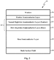
Fig. 3 is a schematic cross-sectional view of a subcell in accordance with another aspect of the disclosure; and -
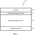
Fig. 4 is a schematic cross-sectional view of a subcell in accordance with yet another aspect of the disclosure. - Referring to
Fig. 1 , one aspect of the disclosed solar cell structure, generally designated 10, may include asolar cell 12, afront contact layer 14, ananti-reflective coating layer 16 and aback contact layer 18. Additional layers, such as a support layer, a reflective layer and/or a cover glass layer, while not shown in the drawings, may be included without departing from the scope of the present disclosure. - The
front contact layer 14 and theanti-reflective coating layer 16 may be positioned over thefront surface 20 of thesolar cell 12 and theback contact layer 18 may be positioned over theback surface 22 of thesolar cell 12. Thesolar cell 12 may produce a voltage across thefront surface 20 and theback surface 22 when thefront surface 20 is exposed to electro-magnetic radiation, such as solar radiation. - The
solar cell 12 may include one ormore subcells 24, 26, 28. In one implementation, thesolar cell 12 may be a multi-junction solar cell that includes atop subcell 24, one or more middle subcells 26 and a bottom subcell 28. For example, the multi-junction solar cell may be a gallium arsenide ("GaAs") solar cell or an inverted metamorphic ("IMM") solar cell. -
Subcell 24 ofsolar cell 12 is shown inFig. 2 . Those skilled in the art will appreciate that anysubcell 24, 26, 28 ofsolar cell 12 may be structured as shown inFig. 2 . In one expression, allsubcells 24, 26, 28 ofsolar cell 12 may be structured as shown inFig. 2 . In another expression, some, but not all,subcells 24, 26, 28 of solar cell 12 (e.g., only the middle 26 and bottom 28 subcells) may be structured as shown inFig. 2 . - Subcell 24 may include a
base semiconductor layer 30, adepletion semiconductor layer 32 and anemitter semiconductor layer 34. Optionally, thesubcell 24 may also include awindow layer 36 positioned over theemitter semiconductor layer 34 and a backsurface field layer 38 positioned over thebase semiconductor layer 30. Other components and layers may also be included insubcell 24 without departing from the scope of the present disclosure. - The
base semiconductor layer 30 may include a first semiconductor material and may have a first bandgap, a first polarity and a cross-sectional thickness TB. - The first semiconductor material of the
base semiconductor layer 30 may be any appropriate semiconductor material. In one specific implementation, the first semiconductor material may be a Group III-V metal or metal alloy. For example, the first semiconductor material may be formed from or may include a Group III-V alloy, such as GaInP, GaAs, GaInAs or InP. - The polarity of the base semiconductor layer 30 (i.e., the first polarity) may be either positive (i.e., p-type) or negative (i.e., n-type). In one example, the
base semiconductor layer 30 may be doped as a p-type semiconductor. In another example, thebase semiconductor layer 30 may be doped as an n-type semiconductor. - The cross-sectional thickness TB of the
base semiconductor layer 30 may depend on various factors, including the composition of thebase semiconductor layer 30. As a general example, thebase semiconductor layer 30 may have a cross-sectional thickness TB ranging from about 0.1 to about 10 microns. As a specific example, thebase semiconductor layer 30 may have a cross-sectional thickness TB of about 1 micron. In one realization, thebase semiconductor layer 30 may define a plane and the cross-sectional thickness TB may be measured perpendicular to that plane. - The
emitter semiconductor layer 34 may include a second semiconductor material and may have a second bandgap, a second polarity and a cross-sectional thickness TE. - In a first implementation, the semiconductor material of the
emitter semiconductor layer 34 may have substantially the same chemical composition as the semiconductor material of the base semiconductor layer 34 (i.e., the first and second semiconductor materials may be the same except for the presence of different dopants or different quantities of dopants). Therefore, in one expression of the first implementation, the bandgap of theemitter semiconductor layer 34 may be substantially the same as the bandgap of the base semiconductor layer 30 (i.e., the first and second bandgaps may be substantially the same). - In another expression of the first implementation, despite being formed from substantially the same materials, the bandgap of the
emitter semiconductor layer 34 may be different than the bandgap of the base semiconductor layer 34 (i.e., the first and second bandgaps may be different). As one example, the bandgap of theemitter semiconductor layer 34 may be greater than the bandgap of thebase semiconductor layer 30. As another example, the bandgap of theemitter semiconductor layer 34 may be smaller than the bandgap of thebase semiconductor layer 34. - In a second implementation, the semiconductor material of the
emitter semiconductor layer 34 may have a different chemical composition than the semiconductor material of the base semiconductor layer 34 (i.e., the first and second semiconductor materials may be different). Therefore, in one expression of the second implementation, the bandgap of theemitter semiconductor layer 34 may be different than the bandgap of the base semiconductor layer 34 (i.e., the first and second bandgaps may be different). As one example, the compositions of theemitter semiconductor layer 34 and thebase semiconductor layer 30 may be engineered to provide thebase semiconductor layer 30 with a greater bandgap than theemitter semiconductor layer 34. As another example, the compositions of theemitter semiconductor layer 34 and thebase semiconductor layer 30 may be engineered to provide theemitter semiconductor layer 34 with a greater bandgap than thebase semiconductor layer 34. - Whether or not the
base semiconductor layer 30 and theemitter semiconductor layer 30 have the same or different chemical compositions, thelayers base semiconductor layer 30 is p-type, theemitter semiconductor layer 34 may be n-type. - The cross-sectional thickness TE of the
emitter semiconductor layer 34 may depend on various factors, including the composition of theemitter semiconductor layer 34. As a general example, theemitter semiconductor layer 34 may have a cross-sectional thickness TE ranging from about 0.01 to about 0.1 microns. As a specific example, theemitter semiconductor layer 34 may have a cross-sectional thickness TE of about 0.05 micron. In one realization, theemitter semiconductor layer 34 may define a plane and the cross-sectional thickness TE may be measured perpendicular to that plane. - The
base semiconductor layer 30 and theemitter semiconductor layer 34 may define a p-n junction having a depletion region 40 between thebase semiconductor layer 30 and theemitter semiconductor layer 34. Thedepletion semiconductor layer 32 may be positioned in, and may overlap and/or eclipse, the depletion region 40. - The
depletion semiconductor layer 32 may include a third semiconductor material and may have a third bandgap, a third polarity and a cross-sectional thickness TD. - The bandgap of the
depletion semiconductor layer 32 may be greater than the bandgap of thebase semiconductor layer 30 and the bandgap of theemitter semiconductor layer 34. Without being limited to any particular theory, it is believed that the higher bandgapdepletion semiconductor layer 32 suppresses recombination in the depletion region 40, thereby resulting in a higher voltage output. - In one embodiment, the bandgap of the
depletion semiconductor layer 32 may be at least 1 percent greater than the bandgap of thebase semiconductor layer 30 and the bandgap of theemitter semiconductor layer 34. In another embodiment, the bandgap of thedepletion semiconductor layer 32 may be at least 1.5 percent greater than the bandgap of thebase semiconductor layer 30 and the bandgap of theemitter semiconductor layer 34. - A high bandgap may be achieved in the
depletion semiconductor layer 32 by altering the composition of thedepletion semiconductor layer 32 relative to thebase 30 andemitter 34 semiconductor layers. Examples of several material systems suitable for forming asubcell 24 wherein thedepletion layer 32 has a higher bandgap than the base 30 andemitter 34 layers are provided in Table 1.Table 1 System Base Layer Depletion Layer Emitter Layer 1 GaInP AlGaInP GaInP 2 GaInP (ordered) GaInP (disordered) GaInP (ordered) 3 GaAs AlGaAs GaAs 4 GaInAs AlGaAs GaInAs 5 GaInAs AlGaInAs GaInAs 6 GaAs GaInPAs GaAs 7 GaInAs GaInPAs GaInAs 8 InP GaInPAs InP 9 InP AlGaInAs InP - The polarity of the
depletion semiconductor layer 32 may correspond to the polarity of either thebase semiconductor layer 30 or theemitter semiconductor layer 34. In a first expression, the polarity of thedepletion semiconductor layer 32 may be the same as the polarity of thebase semiconductor layer 30. As such, thedepletion semiconductor layer 32 may effectively be part of thebase semiconductor layer 30. In a second expression, the polarity of thedepletion semiconductor layer 32 may be the same as the polarity of theemitter semiconductor layer 34. As such, thedepletion semiconductor layer 32 may effectively be part of theemitter semiconductor layer 34. - The cross-sectional thickness TD of the
depletion semiconductor layer 32 may be engineered to be substantially the same as the cross-sectional thickness (i.e., the width) of the depletion region 40. Those skilled in the art will appreciate that the width of the depletion region 40 may depend on the properties of thebase 30 andemitter 34 semiconductor layers that define the depletion region 40. - As a general example, the
depletion semiconductor layer 32 may have a cross-sectional thickness TD ranging from about 0.1 to about 1 microns. As a specific example, thedepletion semiconductor layer 32 may have a cross-sectional thickness TD of about 0.5 microns. In one realization, thedepletion semiconductor layer 32 may define a plane and the cross-sectional thickness TD may be measured perpendicular to that plane. - As one specific, non-limiting example, subcell 24 may be formed from GaInP and GaAlInP using a metal organic vapor phase epitaxy process to grow the
layers base semiconductor layer 30 may be disordered GaInP having a bandgap of 1.89 eV and a cross-sectional thickness TB of about 1.0 microns. Thebase semiconductor layer 30 may be doped as a p-type semiconductor with about 5x10¹⁷ atoms/cm2. Thedepletion semiconductor layer 32 may be GaAlInP having a bandgap of 1.92 to 1.95 eV and a cross-sectional thickness TD of about 0.5 microns. Thedepletion semiconductor layer 32 may be doped as a p-type semiconductor with about 1x10¹⁶ atoms/cm2. Theemitter semiconductor layer 34 may be disordered GaInP having a bandgap of 1.89 eV and a cross-sectional thickness TE of about 0.05 microns. Theemitter semiconductor layer 34 may be doped as an n-type semiconductor with about 5x10¹⁸ atoms/cm2. - Those skilled in the art will appreciate that in some semiconductor material systems, higher bandgap compositions tend to have degraded material properties, such as minority carrier lifetime, mobility and diffusion length. For example, in the AlGaInP/GaInP system, AlGaInP can be used to achieve higher band gaps than GaInP at the same lattice constant, but the strong Al-O bond tends to increase oxygen contamination in AlGaInP. For this reason, and perhaps others, minority hole and minority electron lifetime and mobility are typically lower in AlGaInP than in GaInP. The low hole diffusion length in n-type AlGaInP results in low collection probability for carriers photogenerated in the
emitter semiconductor layer 34 by short wavelengths of light (low blue response). By using Al-free GaInP for theemitter semiconductor layer 34, much longer hole diffusion lengths can be achieved, resulting in significantly greater blue response than with a Al-containing AlGaInP emitter layer, in spite of the small barrier to carrier flow that could be introduced by the high band gap AlGaInP layer in the depletion region 40. The electric field is high in the depletion region 40, which greatly facilitates carrier collection, even if the AlGaInP used there has relatively low carrier lifetime and mobility. - Similarly, if part or all of the
base semiconductor layer 30 is formed using the better material properties of GaInP, while leaving the higher bandgap AlGaInP in the depletion region 40 to increase voltage, carrier collection from that Al-free GaInP portion of the p-typebase semiconductor layer 30 will benefit from the high minority electron lifetime and mobility of p-type GaInP in thebase semiconductor layer 30. - Referring to
Fig. 3 , in another aspect, subcell 12 may include two or more depletion semiconductor layers 32, 33 positioned in the depletion region 40 between the base 30 andemitter 34 semiconductor layers. Eachdepletion semiconductor layer emitter 34 semiconductor layers. The firstdepletion semiconductor layer 32 may have the same polarity as thebase semiconductor layer 30 and may effectively be part of thebase semiconductor layer 30, and the seconddepletion semiconductor layer 33 may have the same polarity as theemitter semiconductor layer 34 and may effectively be part of thebase semiconductor layer 30. - Thus, although the depletion region 40 is typically mostly in the
base semiconductor layer 30, it also necessarily extends somewhat into theemitter semiconductor layer 34. Therefore, introducing a higher bandgap depletion semiconductor layers 32, 33 to both thebase 30 andemitter 34 layers may further suppress recombination and raise cell voltage. - Accordingly, the disclosed
subcell 24 may includes one or more depletion semiconductor layers 32, 33 formed from a higher bandgap material. Thedepletion semiconductor layer 32 may overlap the depletion region 40 between thebase semiconductor layer 30 and theemitter semiconductor 34. The higher bandgap depletion semiconductor layers 32, 33 may lower dark current output and may increase output voltage. Therefore, by limiting the higher bandgap semiconductor material to just a small fraction of thesubcell 24, the remainder of the subcell 24 (e.g., thebase semiconductor layer 30 and emitter semiconductor layer 34) may be optimized for current generation independently, thereby de-coupling current generation from voltage performance. - Referring to
Fig. 4 , in yet another aspect, asubcell 50 may include abase semiconductor layer 52, anemitter semiconductor layer 54 and, optionally, a backsurface field layer 56 and a window layer. Thebase semiconductor layer 52 may have a higher bandgap than theemitter semiconductor layer 54. - A solar cell may comprise a base semiconductor layer having a first bandgap, an emitter semiconductor layer having a second bandgap and a depletion semiconductor layer positioned between said base semiconductor layer and said emitter semiconductor layer said depletion semiconductor layer having a third bandgap, wherein said third bandgap is greater than said first bandgap and said second bandgap. The solar cell may also comprise a first bandgap is substantially the same as said second bandgap. The solar cell may also comprise the first bandgap is greater than said second bandgap. The solar cell may also comprise the third bandgap is at least 1 percent greater than said first bandgap and said second bandgap. The solar cell may also comprise third bandgap is at least 1.5 percent greater than said first bandgap and said second bandgap. The solar cell may also comprise the base semiconductor layer comprises a p-type semiconductor material and said emitter semiconductor layer comprises an n-type semiconductor material. The solar cell may also comprise the depletion semiconductor layer comprises a p-type semiconductor material. The solar cell may also comprise a second depletion semiconductor layer positioned between said depletion semiconductor layer and said emitter semiconductor layer. The solar cell may also comprise the second depletion semiconductor layer comprises an n-type semiconductor material. The solar cell may also comprise the base semiconductor layer and said emitter semiconductor layer define a depletion region having a first cross-sectional thickness (33) and wherein said depletion semiconductor layer has a second cross-sectional thickness (34), said second cross-sectional thickness being substantially equal to said first cross-sectional thickness. The solar cell may also comprise the depletion semiconductor layer fully eclipses said depletion region (40). The solar cell may also comprise the depletion semiconductor layer has a cross-sectional thickness ranging from about 0.1 to about 1 microns. The solar cell may also comprise the base semiconductor layer comprises a first semiconductor composition and said emitter semiconductor layer comprises a second semiconductor composition, and wherein said first semiconductor composition is substantially the same as said second semiconductor composition. The solar cell may also comprise the base semiconductor layer comprises a first semiconductor composition, said emitter semiconductor layer comprises a second semiconductor composition and said depletion semiconductor layer comprises a third semiconductor composition, and wherein said third semiconductor composition is different than said first and said second semiconductor compositions. The solar cell may also comprise each of the base, the depletion and the emitter semiconductor layers comprises a Group III-V alloy. The solar cell may also comprise the depletion semiconductor layer comprises aluminum and wherein at least one of said base semiconductor layer and said emitter semiconductor layer is substantially free of aluminum.
- A solar cell comprising a plurality of subcells, wherein at least one subcell of said plurality of subcells comprises a base semiconductor layer having a first bandgap, an emitter semiconductor layer having a second bandgap and a depletion semiconductor layer positioned between said base semiconductor layer and said emitter semiconductor layer, said depletion semiconductor layer having a third bandgap, wherein said third bandgap is greater than said first bandgap and said second bandgap.
- A solar cell comprising a base semiconductor layer having a first bandgap and an emitter semiconductor layer having a second bandgap, wherein said base semiconductor layer and said emitter semiconductor layer define a p-n junction, and wherein said second bandgap is greater than said first bandgap.
- Although various aspects of the disclosed heterojunction solar cell have been shown and described, modifications may occur to those skilled in the art upon reading the specification. The present application includes such modifications and is limited only by the scope of the claims.
- Further, the disclosure comprises the following clauses:
- 1. A solar cell comprising:
- a base semiconductor layer having a first bandgap;
- an emitter semiconductor layer having a second bandgap; and
- a depletion semiconductor layer positioned between said base semiconductor layer and said emitter semiconductor layer, said depletion semiconductor layer having a third bandgap,
- wherein said third bandgap is greater than said first bandgap and said second bandgap.
- 2. The solar cell of clause 1 wherein said first bandgap is substantially the same as said second bandgap.
- 3. The solar cell of clause 1 wherein said first bandgap is greater than said second bandgap.
- 4. The solar cell of clause 1 wherein said third bandgap is at least 1 percent greater than said first bandgap and said second bandgap.
- 5. The solar cell of clause 1 wherein said third bandgap is at least 1.5 percent greater than said first bandgap and said second bandgap.
- 6. The solar cell of clause 1 wherein said base semiconductor layer comprises a p-type semiconductor material and said emitter semiconductor layer comprises an n-type semiconductor material.
- 7. The solar cell of clause 6 wherein said wherein said depletion semiconductor layer comprises a p-type semiconductor material.
- 8. The solar cell of clause 7 further comprising a second depletion semiconductor layer positioned between said depletion semiconductor layer and said emitter semiconductor layer.
- 9. The solar cell of clause 8 wherein said second depletion semiconductor layer comprises an n-type semiconductor material.
- 10. The solar cell of clause 1 wherein said base semiconductor layer and said emitter semiconductor layer define a depletion region having a first cross-sectional thickness, and wherein said depletion semiconductor layer has a second cross-sectional thickness, said second cross-sectional thickness being substantially equal to said first cross-sectional thickness.
- 11. The solar cell of clause 1 wherein said depletion semiconductor layer fully eclipses said depletion region.
- 12. The solar cell of clause 1 wherein said depletion semiconductor layer has a cross-sectional thickness ranging from about 0.1 to about 1 microns.
- 13. The solar cell of clause 1 wherein said base semiconductor layer comprises a first semiconductor composition and said emitter semiconductor layer comprises a second semiconductor composition, and wherein said first semiconductor composition is substantially the same as said second semiconductor composition.
- 14. The solar cell of clause 1 wherein said base semiconductor layer comprises a first semiconductor composition, said emitter semiconductor layer comprises a second semiconductor composition and said depletion semiconductor layer comprises a third semiconductor composition, and wherein said third semiconductor composition is different than said first and said second semiconductor compositions.
- 15. The solar cell of clause 1 wherein each of said base, said depletion and said emitter semiconductor layers comprises a Group III-V alloy.
- 16. The solar cell of clause 1 wherein said depletion semiconductor layer comprises aluminum and wherein at least one of said base semiconductor layer and said emitter semiconductor layer is substantially free of aluminum.
- 17. A solar cell comprising:
a plurality of subcells, wherein at least one subcell of said plurality of subcells comprises:- a base semiconductor layer having a first bandgap;
- an emitter semiconductor layer having a second bandgap; and
- a depletion semiconductor layer positioned between said base semiconductor layer and said emitter semiconductor layer, said depletion semiconductor layer having a third bandgap,
- wherein said third bandgap is greater than said first bandgap and said second bandgap.
- 18. A solar cell comprising:
- a base semiconductor layer having a first bandgap; and
- an emitter semiconductor layer having a second bandgap,
- wherein said base semiconductor layer and said emitter semiconductor layer define a p-n junction, and
- wherein said second bandgap is greater than said first bandgap.
Claims (15)
- A solar cell comprising:a base semiconductor layer (30) having a first bandgap, wherein the base semiconductor layer (30) comprises a p-type semiconductor material; andan emitter semiconductor layer (34) having a second bandgap, wherein the emitter semiconductor layer (34) comprises an n-type semiconductor material; anda depletion semiconductor layer (32) having a third bandgap, wherein said third bandgap is greater than said first bandgap and said second bandgap, wherein the depletion semiconductor layer (32) comprises a p-type semiconductor material, wherein the depletion semiconductor layer (32) is part of the base semiconductor layer (30);wherein the depletion semiconductor layer (32) of the base semiconductor layer (30) and said emitter semiconductor layer (34) define p-n junction having a depletion region (40) having a first cross-sectional thickness and wherein said depletion semiconductor layer (32) has a second cross-sectional thickness, said second cross-sectional thickness being substantially equal to said first cross-sectional thickness.
- A solar cell comprising:a base semiconductor layer (30) having a first bandgap, wherein the base semiconductor layer (30) comprises a p-type semiconductor material; andan emitter semiconductor layer (34) having a second bandgap, wherein the emitter semiconductor layer (34) comprises an n-type semiconductor material; anda depletion semiconductor layer (32) having a third bandgap, wherein said third bandgap is greater than said first bandgap and said second bandgap, wherein the depletion semiconductor layer (32) comprises an n-type semiconductor material, wherein the depletion semiconductor layer (32) is part of the emitter semiconductor layer (30);wherein the depletion semiconductor layer (32) of the emitter semiconductor layer (30) and said base semiconductor layer (34) define p-n junction having a depletion region (40) having a first cross-sectional thickness and wherein said depletion semiconductor layer (32) has a second cross-sectional thickness, said second cross-sectional thickness being substantially equal to said first cross-sectional thickness.
- A solar cell comprising:a base semiconductor layer (30) having a first bandgap, wherein the base semiconductor layer (30) comprises an n-type semiconductor material; andan emitter semiconductor layer (34) having a second bandgap, wherein the emitter semiconductor layer (34) comprises a p-type semiconductor material; anda depletion semiconductor layer (32) having a third bandgap, wherein said third bandgap is greater than said first bandgap and said second bandgap, wherein the depletion semiconductor layer (32) comprises an n-type semiconductor material, wherein the depletion semiconductor layer (32) is part of the base semiconductor layer (30);wherein the depletion semiconductor layer (32) of the base semiconductor layer (30) and said emitter semiconductor layer (34) define p-n junction having a depletion region (40) having a first cross-sectional thickness and wherein said depletion semiconductor layer (32) has a second cross-sectional thickness, said second cross-sectional thickness being substantially equal to said first cross-sectional thickness.
- A solar cell comprising:a base semiconductor layer (30) having a first bandgap, wherein the base semiconductor layer (30) comprises an n-type semiconductor material; andan emitter semiconductor layer (34) having a second bandgap, wherein the emitter semiconductor layer (34) comprises an p-type semiconductor material; anda depletion semiconductor layer (32) having a third bandgap, wherein said third bandgap is greater than said first bandgap and said second bandgap, wherein the depletion semiconductor layer (32) comprises a p-type semiconductor material, wherein the depletion semiconductor layer (32) is part of the emitter semiconductor layer (30);wherein the depletion semiconductor layer (32) of the emitter semiconductor layer (30) and said base semiconductor layer (34) define p-n junction having a depletion region (40) having a first cross-sectional thickness and wherein said depletion semiconductor layer (32) has a second cross-sectional thickness, said second cross-sectional thickness being substantially equal to said first cross-sectional thickness.
- The solar cell of any of claims 1 to 4, wherein said first bandgap is substantially the same as said second bandgap.
- The solar cell of any of claims 1 to 4, wherein said first bandgap is greater than said second bandgap.
- The solar cell of any of claims 1 to 4, wherein said third bandgap is at least 1 percent greater than said first bandgap and said second bandgap.
- The solar cell of claim 1 or 3, further comprising a second depletion semiconductor layer (33) as part of the emitter semiconductor layer (34).
- The solar cell of claim 8 either: when dependent on claim 1, wherein said second depletion semiconductor layer (33) comprises an n-type semiconductor material; or, when dependent on claim 3, wherein said second depletion semiconductor layer (33) comprises a p-type semiconductor material.
- The solar cell of claim 2 or 4, further comprising a second depletion semiconductor layer (33) as part of the base semiconductor layer (34).
- The solar cell of claim 10 either: when dependent on claim 2, wherein said second depletion semiconductor layer (33) comprises a p-type semiconductor material; or, when dependent on claim 4, wherein said second depletion semiconductor layer (33) comprises an n-type semiconductor material.
- The solar cell of any of claims 1 to 4, wherein said depletion semiconductor layer (32) has a cross-sectional thickness (TD) ranging from about 0.1 to about 1 microns.
- The solar cell of any of claims 1 to 4, wherein said base semiconductor layer (30) comprises a first semiconductor composition and said emitter semiconductor layer (34) comprises a second semiconductor composition, and wherein said first semiconductor composition is substantially the same as said second semiconductor composition.
- The solar cell of any of claims 1 to 4, wherein said base semiconductor layer (30) comprises a first semiconductor composition, said emitter semiconductor layer (34) comprises a second semiconductor composition and said depletion semiconductor layer (32) comprises a third semiconductor composition, and wherein said third semiconductor composition is different than said first and said second semiconductor compositions.
- The solar cell of any of claims 1 to 4, wherein said depletion semiconductor layer (32) comprises aluminum and wherein at least one of said base semiconductor layer (30) and said emitter semiconductor layer (34) is substantially free of aluminum.
Applications Claiming Priority (3)
| Application Number | Priority Date | Filing Date | Title |
|---|---|---|---|
| US12/852,574 US8642883B2 (en) | 2010-08-09 | 2010-08-09 | Heterojunction solar cell |
| PCT/US2011/043124 WO2012021227A2 (en) | 2010-08-09 | 2011-07-07 | Heterojunction solar cell |
| EP11738883.5A EP2603934A2 (en) | 2010-08-09 | 2011-07-07 | Heterojunction solar cell |
Related Parent Applications (1)
| Application Number | Title | Priority Date | Filing Date |
|---|---|---|---|
| EP11738883.5A Division EP2603934A2 (en) | 2010-08-09 | 2011-07-07 | Heterojunction solar cell |
Publications (2)
| Publication Number | Publication Date |
|---|---|
| EP3550617A1 true EP3550617A1 (en) | 2019-10-09 |
| EP3550617B1 EP3550617B1 (en) | 2021-12-15 |
Family
ID=44629419
Family Applications (2)
| Application Number | Title | Priority Date | Filing Date |
|---|---|---|---|
| EP19157479.7A Active EP3550617B1 (en) | 2010-08-09 | 2011-07-07 | Heterojunction solar cell |
| EP11738883.5A Ceased EP2603934A2 (en) | 2010-08-09 | 2011-07-07 | Heterojunction solar cell |
Family Applications After (1)
| Application Number | Title | Priority Date | Filing Date |
|---|---|---|---|
| EP11738883.5A Ceased EP2603934A2 (en) | 2010-08-09 | 2011-07-07 | Heterojunction solar cell |
Country Status (5)
| Country | Link |
|---|---|
| US (1) | US8642883B2 (en) |
| EP (2) | EP3550617B1 (en) |
| JP (2) | JP6199185B2 (en) |
| CA (1) | CA2804222C (en) |
| WO (1) | WO2012021227A2 (en) |
Families Citing this family (31)
| Publication number | Priority date | Publication date | Assignee | Title |
|---|---|---|---|---|
| TW201031006A (en) * | 2008-10-23 | 2010-08-16 | Alta Devices Inc | Photovoltaic device with increased light trapping |
| WO2010048543A2 (en) * | 2008-10-23 | 2010-04-29 | Alta Devices, Inc. | Thin absorber layer of a photovoltaic device |
| EP2351097A2 (en) * | 2008-10-23 | 2011-08-03 | Alta Devices, Inc. | Photovoltaic device |
| US20120104460A1 (en) | 2010-11-03 | 2012-05-03 | Alta Devices, Inc. | Optoelectronic devices including heterojunction |
| US20100319764A1 (en) * | 2009-06-23 | 2010-12-23 | Solar Junction Corp. | Functional Integration Of Dilute Nitrides Into High Efficiency III-V Solar Cells |
| US9691921B2 (en) | 2009-10-14 | 2017-06-27 | Alta Devices, Inc. | Textured metallic back reflector |
| US20150380576A1 (en) | 2010-10-13 | 2015-12-31 | Alta Devices, Inc. | Optoelectronic device with dielectric layer and method of manufacture |
| US9502594B2 (en) | 2012-01-19 | 2016-11-22 | Alta Devices, Inc. | Thin-film semiconductor optoelectronic device with textured front and/or back surface prepared from template layer and etching |
| US11271128B2 (en) | 2009-10-23 | 2022-03-08 | Utica Leaseco, Llc | Multi-junction optoelectronic device |
| US20170141256A1 (en) | 2009-10-23 | 2017-05-18 | Alta Devices, Inc. | Multi-junction optoelectronic device with group iv semiconductor as a bottom junction |
| US9768329B1 (en) | 2009-10-23 | 2017-09-19 | Alta Devices, Inc. | Multi-junction optoelectronic device |
| US20110114163A1 (en) * | 2009-11-18 | 2011-05-19 | Solar Junction Corporation | Multijunction solar cells formed on n-doped substrates |
| US10283657B1 (en) * | 2010-01-08 | 2019-05-07 | Magnolia Optical Technologies, Inc. | Broadband photovoltaic sheets and method of constructing the same |
| US20110232730A1 (en) | 2010-03-29 | 2011-09-29 | Solar Junction Corp. | Lattice matchable alloy for solar cells |
| US9214580B2 (en) | 2010-10-28 | 2015-12-15 | Solar Junction Corporation | Multi-junction solar cell with dilute nitride sub-cell having graded doping |
| US8962991B2 (en) | 2011-02-25 | 2015-02-24 | Solar Junction Corporation | Pseudomorphic window layer for multijunction solar cells |
| WO2013074530A2 (en) | 2011-11-15 | 2013-05-23 | Solar Junction Corporation | High efficiency multijunction solar cells |
| US11038080B2 (en) | 2012-01-19 | 2021-06-15 | Utica Leaseco, Llc | Thin-film semiconductor optoelectronic device with textured front and/or back surface prepared from etching |
| CN102623524A (en) * | 2012-04-06 | 2012-08-01 | 中国科学院苏州纳米技术与纳米仿生研究所 | Semiconductor solar battery and manufacturing method thereof |
| US9153724B2 (en) * | 2012-04-09 | 2015-10-06 | Solar Junction Corporation | Reverse heterojunctions for solar cells |
| US8767867B1 (en) | 2012-05-16 | 2014-07-01 | Cypress Semiconductor Corporation | Integrated control of power supply and power line communications |
| US9530911B2 (en) * | 2013-03-14 | 2016-12-27 | The Boeing Company | Solar cell structures for improved current generation and collection |
| US9590131B2 (en) * | 2013-03-27 | 2017-03-07 | Alliance For Sustainable Energy, Llc | Systems and methods for advanced ultra-high-performance InP solar cells |
| SG11201606353TA (en) | 2014-02-05 | 2016-09-29 | Solar Junction Corp | Monolithic multijunction power converter |
| US20170110613A1 (en) | 2015-10-19 | 2017-04-20 | Solar Junction Corporation | High efficiency multijunction photovoltaic cells |
| RU2611569C1 (en) * | 2015-12-09 | 2017-02-28 | Федеральное государственное бюджетное учреждение науки Физико-технический институт им. А.Ф. Иоффе Российской академии наук | Metamorphic photovoltaic converter |
| DE102016208113B4 (en) * | 2016-05-11 | 2022-07-07 | Fraunhofer-Gesellschaft zur Förderung der angewandten Forschung e.V. | Multi-junction solar cell and its use |
| KR101931712B1 (en) * | 2016-12-28 | 2018-12-24 | 엘지전자 주식회사 | Compound semiconductor solar cell |
| WO2019010037A1 (en) | 2017-07-06 | 2019-01-10 | Solar Junction Corporation | Hybrid mocvd/mbe epitaxial growth of high-efficiency lattice-matched multijunction solar cells |
| EP3669402A1 (en) | 2017-09-27 | 2020-06-24 | Array Photonics, Inc. | Short wavelength infrared optoelectronic devices having a dilute nitride layer |
| US11211514B2 (en) | 2019-03-11 | 2021-12-28 | Array Photonics, Inc. | Short wavelength infrared optoelectronic devices having graded or stepped dilute nitride active regions |
Citations (2)
| Publication number | Priority date | Publication date | Assignee | Title |
|---|---|---|---|---|
| US6300557B1 (en) * | 1998-10-09 | 2001-10-09 | Midwest Research Institute | Low-bandgap double-heterostructure InAsP/GaInAs photovoltaic converters |
| US20100096010A1 (en) * | 2008-10-17 | 2010-04-22 | Kopin Corporation | Ingap heterojunction barrier solar cells |
Family Cites Families (11)
| Publication number | Priority date | Publication date | Assignee | Title |
|---|---|---|---|---|
| JPS5513939A (en) * | 1978-07-17 | 1980-01-31 | Shunpei Yamazaki | Photoelectronic conversion semiconductor device |
| JPS6235681A (en) * | 1985-08-09 | 1987-02-16 | Canon Inc | Photoelectric conversion element |
| GB8524070D0 (en) * | 1985-09-30 | 1985-11-06 | Gen Electric Co Plc | Semiconductor devices |
| JPH0936399A (en) * | 1995-07-25 | 1997-02-07 | Oki Electric Ind Co Ltd | Solar cell |
| JP2000332268A (en) * | 1999-05-19 | 2000-11-30 | Mitsubishi Heavy Ind Ltd | Thin-film polycrystalline silicon, solar battery using the same, and manufacture of thin-film polycrystalline silicon |
| JP2004296658A (en) * | 2003-03-26 | 2004-10-21 | Sharp Corp | Multijunction solar cell and current matching method thereof |
| JP2004319934A (en) * | 2003-04-21 | 2004-11-11 | Sharp Corp | Multi-junction solar cell and manufacturing method thereof |
| US10069026B2 (en) | 2005-12-19 | 2018-09-04 | The Boeing Company | Reduced band gap absorber for solar cells |
| US20090078310A1 (en) | 2007-09-24 | 2009-03-26 | Emcore Corporation | Heterojunction Subcells In Inverted Metamorphic Multijunction Solar Cells |
| US20100006143A1 (en) * | 2007-04-26 | 2010-01-14 | Welser Roger E | Solar Cell Devices |
| US20100147366A1 (en) | 2008-12-17 | 2010-06-17 | Emcore Solar Power, Inc. | Inverted Metamorphic Multijunction Solar Cells with Distributed Bragg Reflector |
-
2010
- 2010-08-09 US US12/852,574 patent/US8642883B2/en active Active
-
2011
- 2011-07-07 CA CA2804222A patent/CA2804222C/en active Active
- 2011-07-07 WO PCT/US2011/043124 patent/WO2012021227A2/en not_active Ceased
- 2011-07-07 EP EP19157479.7A patent/EP3550617B1/en active Active
- 2011-07-07 EP EP11738883.5A patent/EP2603934A2/en not_active Ceased
- 2011-07-07 JP JP2013524080A patent/JP6199185B2/en active Active
-
2017
- 2017-08-22 JP JP2017159338A patent/JP6397975B2/en active Active
Patent Citations (2)
| Publication number | Priority date | Publication date | Assignee | Title |
|---|---|---|---|---|
| US6300557B1 (en) * | 1998-10-09 | 2001-10-09 | Midwest Research Institute | Low-bandgap double-heterostructure InAsP/GaInAs photovoltaic converters |
| US20100096010A1 (en) * | 2008-10-17 | 2010-04-22 | Kopin Corporation | Ingap heterojunction barrier solar cells |
Also Published As
| Publication number | Publication date |
|---|---|
| EP2603934A2 (en) | 2013-06-19 |
| WO2012021227A2 (en) | 2012-02-16 |
| WO2012021227A3 (en) | 2012-12-27 |
| EP3550617B1 (en) | 2021-12-15 |
| JP2018014505A (en) | 2018-01-25 |
| JP6397975B2 (en) | 2018-09-26 |
| JP2013533645A (en) | 2013-08-22 |
| US8642883B2 (en) | 2014-02-04 |
| US20120031478A1 (en) | 2012-02-09 |
| CA2804222C (en) | 2018-02-20 |
| JP6199185B2 (en) | 2017-09-20 |
| CA2804222A1 (en) | 2012-02-16 |
Similar Documents
| Publication | Publication Date | Title |
|---|---|---|
| EP3550617B1 (en) | Heterojunction solar cell | |
| US9985152B2 (en) | Lattice matchable alloy for solar cells | |
| US10355159B2 (en) | Multi-junction solar cell with dilute nitride sub-cell having graded doping | |
| CN101740663A (en) | Method of manufacturing solar cell | |
| CN106549069B (en) | Antimonide-based high-bandgap tunnel junctions for semiconductor devices | |
| US20130104970A1 (en) | Four junction solar cell | |
| US10944022B2 (en) | Solar cell with delta doping layer | |
| US20190288147A1 (en) | Dilute nitride optical absorption layers having graded doping | |
| CN103000740A (en) | GaAs/GaInP double knot solar battery and manufacturing method thereof | |
| EP3980586A1 (en) | Dilute nitride optical absorption layers having graded doping | |
| CN110534598A (en) | A kind of compound solar cell containing superlattice structure back surface field | |
| Lü et al. | AlGaAs/GaAs tunnel junctions in a 4-J tandem solar cell |
Legal Events
| Date | Code | Title | Description |
|---|---|---|---|
| PUAI | Public reference made under article 153(3) epc to a published international application that has entered the european phase |
Free format text: ORIGINAL CODE: 0009012 |
|
| STAA | Information on the status of an ep patent application or granted ep patent |
Free format text: STATUS: THE APPLICATION HAS BEEN PUBLISHED |
|
| AC | Divisional application: reference to earlier application |
Ref document number: 2603934 Country of ref document: EP Kind code of ref document: P |
|
| AK | Designated contracting states |
Kind code of ref document: A1 Designated state(s): AL AT BE BG CH CY CZ DE DK EE ES FI FR GB GR HR HU IE IS IT LI LT LU LV MC MK MT NL NO PL PT RO RS SE SI SK SM TR |
|
| STAA | Information on the status of an ep patent application or granted ep patent |
Free format text: STATUS: REQUEST FOR EXAMINATION WAS MADE |
|
| 17P | Request for examination filed |
Effective date: 20200317 |
|
| RBV | Designated contracting states (corrected) |
Designated state(s): AL AT BE BG CH CY CZ DE DK EE ES FI FR GB GR HR HU IE IS IT LI LT LU LV MC MK MT NL NO PL PT RO RS SE SI SK SM TR |
|
| STAA | Information on the status of an ep patent application or granted ep patent |
Free format text: STATUS: EXAMINATION IS IN PROGRESS |
|
| 17Q | First examination report despatched |
Effective date: 20200618 |
|
| GRAP | Despatch of communication of intention to grant a patent |
Free format text: ORIGINAL CODE: EPIDOSNIGR1 |
|
| STAA | Information on the status of an ep patent application or granted ep patent |
Free format text: STATUS: GRANT OF PATENT IS INTENDED |
|
| INTG | Intention to grant announced |
Effective date: 20210709 |
|
| GRAS | Grant fee paid |
Free format text: ORIGINAL CODE: EPIDOSNIGR3 |
|
| GRAA | (expected) grant |
Free format text: ORIGINAL CODE: 0009210 |
|
| STAA | Information on the status of an ep patent application or granted ep patent |
Free format text: STATUS: THE PATENT HAS BEEN GRANTED |
|
| AC | Divisional application: reference to earlier application |
Ref document number: 2603934 Country of ref document: EP Kind code of ref document: P |
|
| AK | Designated contracting states |
Kind code of ref document: B1 Designated state(s): AL AT BE BG CH CY CZ DE DK EE ES FI FR GB GR HR HU IE IS IT LI LT LU LV MC MK MT NL NO PL PT RO RS SE SI SK SM TR |
|
| REG | Reference to a national code |
Ref country code: GB Ref legal event code: FG4D Ref country code: CH Ref legal event code: EP |
|
| REG | Reference to a national code |
Ref country code: DE Ref legal event code: R096 Ref document number: 602011072282 Country of ref document: DE |
|
| REG | Reference to a national code |
Ref country code: IE Ref legal event code: FG4D |
|
| REG | Reference to a national code |
Ref country code: AT Ref legal event code: REF Ref document number: 1456142 Country of ref document: AT Kind code of ref document: T Effective date: 20220115 |
|
| REG | Reference to a national code |
Ref country code: LT Ref legal event code: MG9D |
|
| REG | Reference to a national code |
Ref country code: NL Ref legal event code: MP Effective date: 20211215 |
|
| PG25 | Lapsed in a contracting state [announced via postgrant information from national office to epo] |
Ref country code: RS Free format text: LAPSE BECAUSE OF FAILURE TO SUBMIT A TRANSLATION OF THE DESCRIPTION OR TO PAY THE FEE WITHIN THE PRESCRIBED TIME-LIMIT Effective date: 20211215 Ref country code: LT Free format text: LAPSE BECAUSE OF FAILURE TO SUBMIT A TRANSLATION OF THE DESCRIPTION OR TO PAY THE FEE WITHIN THE PRESCRIBED TIME-LIMIT Effective date: 20211215 Ref country code: FI Free format text: LAPSE BECAUSE OF FAILURE TO SUBMIT A TRANSLATION OF THE DESCRIPTION OR TO PAY THE FEE WITHIN THE PRESCRIBED TIME-LIMIT Effective date: 20211215 Ref country code: BG Free format text: LAPSE BECAUSE OF FAILURE TO SUBMIT A TRANSLATION OF THE DESCRIPTION OR TO PAY THE FEE WITHIN THE PRESCRIBED TIME-LIMIT Effective date: 20220315 |
|
| REG | Reference to a national code |
Ref country code: AT Ref legal event code: MK05 Ref document number: 1456142 Country of ref document: AT Kind code of ref document: T Effective date: 20211215 |
|
| PG25 | Lapsed in a contracting state [announced via postgrant information from national office to epo] |
Ref country code: SE Free format text: LAPSE BECAUSE OF FAILURE TO SUBMIT A TRANSLATION OF THE DESCRIPTION OR TO PAY THE FEE WITHIN THE PRESCRIBED TIME-LIMIT Effective date: 20211215 Ref country code: NO Free format text: LAPSE BECAUSE OF FAILURE TO SUBMIT A TRANSLATION OF THE DESCRIPTION OR TO PAY THE FEE WITHIN THE PRESCRIBED TIME-LIMIT Effective date: 20220315 Ref country code: LV Free format text: LAPSE BECAUSE OF FAILURE TO SUBMIT A TRANSLATION OF THE DESCRIPTION OR TO PAY THE FEE WITHIN THE PRESCRIBED TIME-LIMIT Effective date: 20211215 Ref country code: HR Free format text: LAPSE BECAUSE OF FAILURE TO SUBMIT A TRANSLATION OF THE DESCRIPTION OR TO PAY THE FEE WITHIN THE PRESCRIBED TIME-LIMIT Effective date: 20211215 Ref country code: GR Free format text: LAPSE BECAUSE OF FAILURE TO SUBMIT A TRANSLATION OF THE DESCRIPTION OR TO PAY THE FEE WITHIN THE PRESCRIBED TIME-LIMIT Effective date: 20220316 |
|
| PG25 | Lapsed in a contracting state [announced via postgrant information from national office to epo] |
Ref country code: NL Free format text: LAPSE BECAUSE OF FAILURE TO SUBMIT A TRANSLATION OF THE DESCRIPTION OR TO PAY THE FEE WITHIN THE PRESCRIBED TIME-LIMIT Effective date: 20211215 |
|
| PG25 | Lapsed in a contracting state [announced via postgrant information from national office to epo] |
Ref country code: SM Free format text: LAPSE BECAUSE OF FAILURE TO SUBMIT A TRANSLATION OF THE DESCRIPTION OR TO PAY THE FEE WITHIN THE PRESCRIBED TIME-LIMIT Effective date: 20211215 Ref country code: SK Free format text: LAPSE BECAUSE OF FAILURE TO SUBMIT A TRANSLATION OF THE DESCRIPTION OR TO PAY THE FEE WITHIN THE PRESCRIBED TIME-LIMIT Effective date: 20211215 Ref country code: RO Free format text: LAPSE BECAUSE OF FAILURE TO SUBMIT A TRANSLATION OF THE DESCRIPTION OR TO PAY THE FEE WITHIN THE PRESCRIBED TIME-LIMIT Effective date: 20211215 Ref country code: PT Free format text: LAPSE BECAUSE OF FAILURE TO SUBMIT A TRANSLATION OF THE DESCRIPTION OR TO PAY THE FEE WITHIN THE PRESCRIBED TIME-LIMIT Effective date: 20220418 Ref country code: ES Free format text: LAPSE BECAUSE OF FAILURE TO SUBMIT A TRANSLATION OF THE DESCRIPTION OR TO PAY THE FEE WITHIN THE PRESCRIBED TIME-LIMIT Effective date: 20211215 Ref country code: EE Free format text: LAPSE BECAUSE OF FAILURE TO SUBMIT A TRANSLATION OF THE DESCRIPTION OR TO PAY THE FEE WITHIN THE PRESCRIBED TIME-LIMIT Effective date: 20211215 Ref country code: CZ Free format text: LAPSE BECAUSE OF FAILURE TO SUBMIT A TRANSLATION OF THE DESCRIPTION OR TO PAY THE FEE WITHIN THE PRESCRIBED TIME-LIMIT Effective date: 20211215 |
|
| PG25 | Lapsed in a contracting state [announced via postgrant information from national office to epo] |
Ref country code: PL Free format text: LAPSE BECAUSE OF FAILURE TO SUBMIT A TRANSLATION OF THE DESCRIPTION OR TO PAY THE FEE WITHIN THE PRESCRIBED TIME-LIMIT Effective date: 20211215 Ref country code: AT Free format text: LAPSE BECAUSE OF FAILURE TO SUBMIT A TRANSLATION OF THE DESCRIPTION OR TO PAY THE FEE WITHIN THE PRESCRIBED TIME-LIMIT Effective date: 20211215 |
|
| REG | Reference to a national code |
Ref country code: DE Ref legal event code: R097 Ref document number: 602011072282 Country of ref document: DE |
|
| PG25 | Lapsed in a contracting state [announced via postgrant information from national office to epo] |
Ref country code: IS Free format text: LAPSE BECAUSE OF FAILURE TO SUBMIT A TRANSLATION OF THE DESCRIPTION OR TO PAY THE FEE WITHIN THE PRESCRIBED TIME-LIMIT Effective date: 20220415 |
|
| PLBE | No opposition filed within time limit |
Free format text: ORIGINAL CODE: 0009261 |
|
| STAA | Information on the status of an ep patent application or granted ep patent |
Free format text: STATUS: NO OPPOSITION FILED WITHIN TIME LIMIT |
|
| PG25 | Lapsed in a contracting state [announced via postgrant information from national office to epo] |
Ref country code: DK Free format text: LAPSE BECAUSE OF FAILURE TO SUBMIT A TRANSLATION OF THE DESCRIPTION OR TO PAY THE FEE WITHIN THE PRESCRIBED TIME-LIMIT Effective date: 20211215 Ref country code: AL Free format text: LAPSE BECAUSE OF FAILURE TO SUBMIT A TRANSLATION OF THE DESCRIPTION OR TO PAY THE FEE WITHIN THE PRESCRIBED TIME-LIMIT Effective date: 20211215 |
|
| 26N | No opposition filed |
Effective date: 20220916 |
|
| PG25 | Lapsed in a contracting state [announced via postgrant information from national office to epo] |
Ref country code: SI Free format text: LAPSE BECAUSE OF FAILURE TO SUBMIT A TRANSLATION OF THE DESCRIPTION OR TO PAY THE FEE WITHIN THE PRESCRIBED TIME-LIMIT Effective date: 20211215 |
|
| PG25 | Lapsed in a contracting state [announced via postgrant information from national office to epo] |
Ref country code: MC Free format text: LAPSE BECAUSE OF FAILURE TO SUBMIT A TRANSLATION OF THE DESCRIPTION OR TO PAY THE FEE WITHIN THE PRESCRIBED TIME-LIMIT Effective date: 20211215 |
|
| REG | Reference to a national code |
Ref country code: CH Ref legal event code: PL |
|
| REG | Reference to a national code |
Ref country code: BE Ref legal event code: MM Effective date: 20220731 |
|
| PG25 | Lapsed in a contracting state [announced via postgrant information from national office to epo] |
Ref country code: LU Free format text: LAPSE BECAUSE OF NON-PAYMENT OF DUE FEES Effective date: 20220707 Ref country code: LI Free format text: LAPSE BECAUSE OF NON-PAYMENT OF DUE FEES Effective date: 20220731 Ref country code: CH Free format text: LAPSE BECAUSE OF NON-PAYMENT OF DUE FEES Effective date: 20220731 |
|
| PG25 | Lapsed in a contracting state [announced via postgrant information from national office to epo] |
Ref country code: IT Free format text: LAPSE BECAUSE OF FAILURE TO SUBMIT A TRANSLATION OF THE DESCRIPTION OR TO PAY THE FEE WITHIN THE PRESCRIBED TIME-LIMIT Effective date: 20211215 Ref country code: BE Free format text: LAPSE BECAUSE OF NON-PAYMENT OF DUE FEES Effective date: 20220731 |
|
| P01 | Opt-out of the competence of the unified patent court (upc) registered |
Effective date: 20230516 |
|
| PG25 | Lapsed in a contracting state [announced via postgrant information from national office to epo] |
Ref country code: IE Free format text: LAPSE BECAUSE OF NON-PAYMENT OF DUE FEES Effective date: 20220707 |
|
| PG25 | Lapsed in a contracting state [announced via postgrant information from national office to epo] |
Ref country code: HU Free format text: LAPSE BECAUSE OF FAILURE TO SUBMIT A TRANSLATION OF THE DESCRIPTION OR TO PAY THE FEE WITHIN THE PRESCRIBED TIME-LIMIT; INVALID AB INITIO Effective date: 20110707 |
|
| PG25 | Lapsed in a contracting state [announced via postgrant information from national office to epo] |
Ref country code: MK Free format text: LAPSE BECAUSE OF FAILURE TO SUBMIT A TRANSLATION OF THE DESCRIPTION OR TO PAY THE FEE WITHIN THE PRESCRIBED TIME-LIMIT Effective date: 20211215 Ref country code: CY Free format text: LAPSE BECAUSE OF FAILURE TO SUBMIT A TRANSLATION OF THE DESCRIPTION OR TO PAY THE FEE WITHIN THE PRESCRIBED TIME-LIMIT Effective date: 20211215 |
|
| PG25 | Lapsed in a contracting state [announced via postgrant information from national office to epo] |
Ref country code: TR Free format text: LAPSE BECAUSE OF FAILURE TO SUBMIT A TRANSLATION OF THE DESCRIPTION OR TO PAY THE FEE WITHIN THE PRESCRIBED TIME-LIMIT Effective date: 20211215 |
|
| PG25 | Lapsed in a contracting state [announced via postgrant information from national office to epo] |
Ref country code: MT Free format text: LAPSE BECAUSE OF FAILURE TO SUBMIT A TRANSLATION OF THE DESCRIPTION OR TO PAY THE FEE WITHIN THE PRESCRIBED TIME-LIMIT Effective date: 20211215 |
|
| REG | Reference to a national code |
Ref country code: DE Ref legal event code: R079 Ref document number: 602011072282 Country of ref document: DE Free format text: PREVIOUS MAIN CLASS: H01L0031072500 Ipc: H10F0010161000 |
|
| PGFP | Annual fee paid to national office [announced via postgrant information from national office to epo] |
Ref country code: DE Payment date: 20250729 Year of fee payment: 15 |
|
| PGFP | Annual fee paid to national office [announced via postgrant information from national office to epo] |
Ref country code: GB Payment date: 20250728 Year of fee payment: 15 |
|
| PGFP | Annual fee paid to national office [announced via postgrant information from national office to epo] |
Ref country code: FR Payment date: 20250725 Year of fee payment: 15 |